1
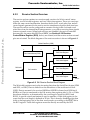
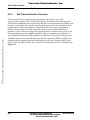
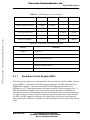
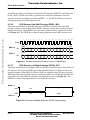
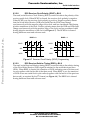
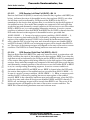
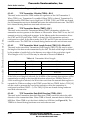
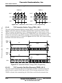
Freescale Semiconductor, Inc.
SECTION 6
Freescale Semiconductor, Inc...
SERIAL AUDIO INTERFACE
MOTOROLA
DSP56004 User’s Manual
For More Information On This Product,
Go to: www.freescale.com
6-1
Freescale Semiconductor, Inc.
Serial Audio Interface
INTRODUCTION . . . . . . . . . . . . . . . . . . . . . . . . . . . . . . . . . . 6-3
SERIAL AUDIO INTERFACE INTERNAL ARCHITECTURE 6-4
SERIAL AUDIO INTERFACE PROGRAMMING MODEL . . . 6-8
PROGRAMMING CONSIDERATIONS . . . . . . . . . . . . . . . . 6-24
Freescale Semiconductor, Inc...
6.1
6.2
6.3
6.4
6-2
DSP56004 User’s Manual
For More Information On This Product,
Go to: www.freescale.com
MOTOROLA
Freescale Semiconductor, Inc.
Serial Audio Interface
Introduction
6.1
INTRODUCTION
The DSP communicates with data sources and sinks through its Serial Audio
Interface (SAI). The SAI is a synchronous serial interface dedicated for audio data
transfers. It provides a full duplex serial port for serial connection with a variety of
audio devices such as Analog-to-Digital (A/D) converters, Digital-to-Analog (D/A)
converters, CD devices, etc. The SAI implements a wide range of serial data formats
currently in use by audio manufacturers. Examples are:
Freescale Semiconductor, Inc...
• I2S (Inter Integrated-circuit Sound) format (Philips)
• CDP format (Sony)
• MEC format (Matsushita)
• Most Industry-Standard A/D and D/A
The SAI consists of independent transmit and receive sections and a shared
baud-rate generator. The transmitter and receiver sections may each operate in either
the Master or Slave mode. In the Master mode the serial clock and the word select
lines are driven internally according to the baud-rate generator programming. In the
Slave mode these signals are supplied from an external source. The transmitter
consists of three transmit-data registers, three fully synchronized output- shift
registers, and three serial-data output lines controlled by one transmitter controller.
This permits data transmission to one, two, or three stereo audio devices
simultaneously. The receiver consists of two receive-data registers, two fully
synchronized input-shift registers, and two serial data input lines controlled by one
receiver controller. This permits data reception from one or two stereo audio devices
simultaneously.
The following is a short list of the SAI features:
• Programmable serial clock generator with high resolution:
fsck = fosc/2i (for i > 1)
• Maximum external serial clock rate equal to one third of the DSP core clock
• Separate transmit and receive sections
• Master or Slave operating modes
• Three synchronized data transmission lines
• Two synchronized data reception lines
• Double-buffered
MOTOROLA
DSP56004 User’s Manual
For More Information On This Product,
Go to: www.freescale.com
6-3
Freescale Semiconductor, Inc.
Serial Audio Interface
Serial Audio Interface Internal Architecture
• User programmable to support a wide variety of serial audio formats
• Three receive interrupt vectors: Receive Left Channel, Receive Right Channel,
and Receive with Exception
• Three transmit interrupt vectors: Transmit Left Channel, Transmit Right
Channel, and Transmit with Exception
Freescale Semiconductor, Inc...
6.2
SERIAL AUDIO INTERFACE INTERNAL ARCHITECTURE
The SAI is functionally divided into three parts: the baud-rate generator, the receiver
section, and the transmitter section. The receive and transmit sections are completely
independent and can operate concurrently or separately. The following paragraphs
describe the operation of these sections.
6.2.1
Baud-Rate Generator
The baud-rate generator produces the internal serial clock for the SAI if either or both
of the receiver and transmitter sections are configured in the Master mode. The
baud-rate generator is disabled if both receiver and transmitter sections are
configured as slaves. Figure 6-1 illustrates the internal clock path connections. The
receiver and transmitter clocks can be internal or external depending on the
configuration of the Receive Master (RMST) and Transmit Master (TMST) control
bits.
TMST = 0
TClock
Tx
SCKT
TMST = 1
TMST
RMST = 0
RClock
Rx
SCKR
RMST = 1
Internal Clock
RMST
FOSC
Divide
By 2
Prescale
Divide By 1
or
Divide By 8
Divider
Divide By 1
To
Divide By 256
PSR
PM0–PM7
AA0427k
Figure 6-1 SAI Baud-Rate Generator Block Diagram
6-4
DSP56004 User’s Manual
For More Information On This Product,
Go to: www.freescale.com
MOTOROLA
Freescale Semiconductor, Inc.
Serial Audio Interface
Serial Audio Interface Internal Architecture
Freescale Semiconductor, Inc...
6.2.2
Receive Section Overview
The receive section contains two receivers and consists of a 16-bit control/status
register, two 24-bit shift registers, and two 24-bit data registers. These two receivers
share the same control mechanism, therefore the bit clock, word select line, and all
control signals generated in the receive section simultaneously affect both receivers.
The receiver section can be configured as a master driving its bit clock and word
select lines from the internal baud-rate generator, or as a slave receiving these signals
from an external source. When both receivers are disabled, the receive controller
becomes idle, the status bits RLDF and RRDF (see Section 6.3.2 Receiver
Control/Status Register (RCS), below) are cleared, and the receive section external
pins are tri-stated. The block diagram of the receiver section is shown in Figure 6-2.
Global Data Bus (GDB)
15
23
0
0
RX0 Data Register
Rx Control/Status (RCS)
23
0
SDI0
RX0 Shift Register
23
RCLOCK
0
Status
RX1 Data Register
Rx Controller
23
0
Control
SDI1
RX1 Shift Register
AA0428
Figure 6-2 SAI Receive Section Block Diagram
The 24-bit shift registers receive the incoming data from the Serial Data In pins (SDI0
and SDI1, or SDIx). Data is shifted in at the transitions of the serial receive clock
SCKR. Data is assumed to be received MSB first if RDIR is cleared, and LSB first if
RDIR is set. Data is transferred to the SAI receive data registers after 16, 24, or 32 bits
have been shifted in, as determined by the word length control bits RWL1 and
RWL0. A special control mechanism is used to emulate a 32-bit shift register in the
event that the word length is defined as 32 bits. This is done by disabling eight data
shifts at the beginning/end of the data word transfer, according to the RDWT bit in
the RCS register. These shift registers cannot be directly accessed by the DSP.
MOTOROLA
DSP56004 User’s Manual
For More Information On This Product,
Go to: www.freescale.com
6-5
Freescale Semiconductor, Inc.
Serial Audio Interface
Serial Audio Interface Internal Architecture
Freescale Semiconductor, Inc...
6.2.3
SAI Transmit Section Overview
The transmit section contains three transmitters and consists of a 16-bit
control/status register, three 24-bit shift registers, and three 24-bit data registers.
These three transmitters are controlled by the same control mechanism, therefore, the
bit clock, word select line, and all control signals generated in the transmit section
equally affect all three transmitters. The transmit section can be configured as a
master driving its bit clock and word select lines from the internal baud-rate
generator, or as a slave receiving these signals from an external source. Each of the
three transmitters can be enabled separately. When a transmitter is disabled, its
associated Serial Data Out (SDO) pin goes to high level. When all transmitters are
disabled, the transmit controller becomes idle, the status bits TRDE and TLDE are
cleared, and the transmit section external pins, Word Select Transmit (WST) and
Serial Clock Transmit (SCKT), are tri-stated. The transmitter section is illustrated in
Figure 6-3.
6-6
DSP56004 User’s Manual
For More Information On This Product,
Go to: www.freescale.com
MOTOROLA
Freescale Semiconductor, Inc.
Serial Audio Interface
Serial Audio Interface Internal Architecture
Global Data Bus (GDB)
23
15
0
0
TX0 Data Register
Transmit Control/Status (TCS)
0
23
SDO0
Freescale Semiconductor, Inc...
TX0 Shift Register
0
23
Status
TCLOCK
TX1 Data Register
Transmit Controller
0
23
Control
SDO1
TX1 Shift Register
23
0
TX2 Data Register
23
0
SDO2
TX2 Shift Register
AA0429k
Figure 6-3 SAI Transmit Section Block Diagram
.
The transmitter section data path consists of three fully synchronized sets of data and
shift registers capable of operating simultaneously. In each set, the 24-bit shift
register contains the data being transmitted. Data is shifted out to the associated SDO
pin at the transitions of the serial transmit clock SCKT. Data is shifted out MSB first if
TDIR is cleared, and LSB first if TDIR is set. The number of bits shifted out before the
shift register is considered empty and ready to be reloaded can be 16, 24, or 32 bits as
determined by the TWL1 and TWL0 control bits in the TCS register. A special control
mechanism is used to emulate a 32-bit shift register if the word length is defined as 32
bits. This is done by enabling eight data shifts at the beginning/end of the data word
transfer, according to the TDWE bit in the TCS register. These shift registers cannot
be directly accessed by the DSP.
MOTOROLA
DSP56004 User’s Manual
For More Information On This Product,
Go to: www.freescale.com
6-7
Freescale Semiconductor, Inc.
Serial Audio Interface
Serial Audio Interface Programming Model
6.3
SERIAL AUDIO INTERFACE PROGRAMMING MODEL
The Serial Audio Interface registers that are available to the programmer are shown
in Figure 6-4. The registers are described in the following paragraphs.
Baud Rate Control Register (BRC) X: $FFE0
23
16
15
14
13
12
11
10
9
8
7
6
5
4
3
2
PSR
PM7
PM6
PM5
PM4
PM3
PM2
3
2
1
0
PM1 PM0
Freescale Semiconductor, Inc...
Receive Control/Status Register (RCS) X: $FFE1
23
16
15
14
13
RRDF RLDF
12
11
10
9
8
7
6
5
4
RXIL RXIE RDWT RREL RCKP RLRS RDIR RWL1 RWL0 RMST
1
0
R1EN R0EN
Transmit Control/Status Register (TCS) X: $FFE4
23
16
15
14
13
TRDE TLDE
12
TXIL
11
10
9
8
7
6
5
4
3
2
1
0
TXIE TDWE TREL TCKP TLRS TDIR TWL1 TWL0 TMST T2EN T1EN T0EN
23
0
Receiver 0 Data Register
read-only
X: $FFE2
23
0
Receiver 1 Data Register
read-only
X: $FFE3
23
0
Transmitter 0 Data Register
write-only
X: $FFE5
23
0
Transmitter 1 Data Register
write-only
X: $FFE6
23
0
Transmitter 2 Data Register
write-only
X: $FFE7
Reserved Bit(s)
AA0430k
Figure 6-4 SAI Registers
The SAI interrupt vectors can be located in either of two different regions in memory.
The transmit interrupt vector locations are controlled by TXIL bit in the Transmit
Control Status (TCS) register. Similarly, the receive interrupt vector locations are
controlled by RXIL bit in the Receive Control Status (RCS) register. The interrupt
vector locations for the SAI are shown in Table 6-1. The interrupts generated by the
SAI are prioritized as shown in Table 6-2.
6-8
DSP56004 User’s Manual
For More Information On This Product,
Go to: www.freescale.com
MOTOROLA
Freescale Semiconductor, Inc.
Serial Audio Interface
Serial Audio Interface Programming Model
Freescale Semiconductor, Inc...
Table 6-1 SAI Interrupt Vector Locations
Interrupt
TXIL = 0
TXIL = 1
RXIL = 0
RXIL = 1
Left Channel Transmit
P: $0010
P: $0040
—
—
Right Channel Transmit
P: $0012
P: $0042
—
—
Transmit Exception
P: $0014
P: $0044
—
—
Left Channel Receive
—
—
P: $0016
P: $0046
Right Channel Receive
—
—
P: $0018
P: $0048
Receive Exception
—
—
P: $001A
P: $004A
Table 6-2 SAI Internal Interrupt Priorities
Priority
Highest
Interrupt
SAI Receive
SAI Transmit
SAI Left Channel Receive
SAI Left Channel Transmit
SAI Right Channel Receive
Lowest
6.3.1
SAI Right Channel Transmit
Baud Rate Control Register (BRC)
The serial clock frequency is determined by the control bits in the Baud Rate Control
register (BRC) as described in the following paragraphs. The BRC is illustrated in
Figure 6-4 on page 6-8. The maximum allowed internally generated bit clock
frequency is fosc/4 and the maximum allowed external bit clock frequency is fosc/3.
BRC bits should be modified only when the baud-rate generator is disabled (i.e.,
when both receiver and transmitter sections are defined as slaves or when both are in
the individual reset state); otherwise improper operation may result. When read by
the DSP, the BRC appears on the two low-order bytes of the 24-bit word, and the
high-order byte is read as 0s. The BRC is cleared during hardware reset and software
reset.
MOTOROLA
DSP56004 User’s Manual
For More Information On This Product,
Go to: www.freescale.com
6-9
Freescale Semiconductor, Inc.
Serial Audio Interface
Serial Audio Interface Programming Model
6.3.1.1
Prescale Modulus select (PM[7:0])—Bits 7–0
The PM[7:0] bits specify the divide ratio of the prescale divider in the SAI baud-rate
generator. A divide ratio between 1 and 256 (PM[7:0] = $00 to $FF) may be selected.
The PM[7:0] bits are cleared during hardware reset and software reset.
Freescale Semiconductor, Inc...
Note: The programmer should not use the combination PSR = 1 and
PM[7:0] = 00000000, since it may cause synchronization problems and
improper operation (it is considered an illegal combination).
6.3.1.2
Prescaler Range (PSR)—Bit 8
The Prescaler Range (PSR) bit controls a fixed divide-by-eight prescaler connected in
series with the variable prescale divider. This bit is used to extend the range of the
prescaler for those cases in which a slower clock rate is desired. When PSR is set, the
fixed prescaler is bypassed. When PSR is cleared, the fixed divide-by-eight prescaler
is operational. The PSR bit is cleared during hardware reset and software reset.
6.3.1.3
BRC Reserved Bits—Bits 15–9
Bits 15–9 in the BRC are reserved and unused. They read as 0s and should be written
with 0s for future compatibility.
6.3.2
Receiver Control/Status Register (RCS)
The Receiver Control/Status register (RCS) is a 16-bit read/write control/status
register used to direct the operation of the receive section in the SAI (see Figure 6-4
on page 6-8). The control bits in the RCS determine the serial format of the data
transfers, whereas the status bits of the RCS are used by the DSP programmer to
interrogate the status of the receiver. Receiver-enable and interrupt-enable bits are
also provided in the RCS. When read by the DSP, the RCS appears on the two
low-order bytes of the 24-bit word, and the high-order byte is read as 0s. Hardware
reset and software reset clear all the bits in the RCS. If both R0EN and R1EN bits are
cleared, the receiver section is disabled and it enters the individual reset state. The
individual reset state is entered 1 instruction cycle after bits R0EN and R1EN are
cleared. While in the Stop or individual reset state, the status bits in RCS are also
cleared. Stop or individual reset do not affect the RCS control bits. The programmer
should change the RCS control bits (except for RXIE) only while the receiver section
is in the individual reset state (i.e., disabled), otherwise improper operation may
result. The RCS bits are described in the following paragraphs.
6.3.2.1
RCS Receiver 0 Enable (R0EN)—Bit 0
The read/write Receiver 0 Enable (R0EN) control bit enables the operation of SAI
Receiver 0. When R0EN is set, Receiver 0 is enabled. When R0EN is cleared, Receiver
0 is disabled. If both R0EN and R1EN are cleared, the receiver section is disabled,
6-10
DSP56004 User’s Manual
For More Information On This Product,
Go to: www.freescale.com
MOTOROLA
Freescale Semiconductor, Inc.
Serial Audio Interface
Serial Audio Interface Programming Model
which is equivalent to the individual reset state. The R0EN bit is cleared during
hardware reset and software reset.
Freescale Semiconductor, Inc...
6.3.2.2
RCS Receiver 1 Enable (R1EN)—Bit 1
The read/write Receiver 1 Enable (R1EN) control bit enables the operation of SAI
Receiver 1. When R1EN is set, Receiver 1 is enabled. When R1EN is cleared, Receiver
1 is disabled. If both R0EN and R1EN are cleared, the receiver section is disabled,
which is equivalent to the individual reset state. The R1EN bit is cleared during
hardware reset and software reset.
6.3.2.3
RCS Reserved Bit—Bits 13 and 2
Bits 13 and 2 in the RCS are reserved and unused. They read as 0s and should be
written with 0s for future compatibility.
6.3.2.4
RCS Receiver Master (RMST)—Bit 3
The read/write control bit Receiver Master (RMST) switches the operation of the
receiver section between Master and Slave modes. When RMST is set, the SAI
receiver section is configured as a master. In the Master mode the receiver drives the
SCKR and WSR pins. When RMST is cleared, the SAI receiver section is configured as
a slave. In the Slave mode, the SCKR and WSR pins are driven from an external
source. The RMST bit is cleared during hardware reset and software reset.
6.3.2.5
RCS Receiver Word Length Control (RWL[1:0])—Bits 4 and 5
The read/write Receiver Word Length (RWL[1:0]) control bits are used to select the
length of the data words received by the SAI. The data word length is defined by the
number of serial clock cycles between two edges of the word select signal. Word
lengths of 16, 24, or 32 bits may be selected as shown in Table 6-3.
Table 6-3 Receiver Word Length Control
RWL1
RWL0
Number of Bits/Word
0
0
16
0
1
24
1
0
32
1
1
Reserved
The receive data registers are always loaded with 24 bits when a new data word
arrives. If the 16-bit word length is selected, the received 16-bit data word will be
placed in the 16 most significant bits of the receive data register, independent of the
Receiver data shift Direction bit (RDIR, see below), while the 8 least significant bits of
the receive data register are cleared. If a 32-bit word length is selected, 8 bits are
MOTOROLA
DSP56004 User’s Manual
For More Information On This Product,
Go to: www.freescale.com
6-11
Freescale Semiconductor, Inc.
Serial Audio Interface
Serial Audio Interface Programming Model
discarded according to the Receiver Data Word Truncation (RDWT) control bit (see
below). RWL[1:0] are also used to generate the word select indication when the
receiver section is configured as master (RMST = 1). The RWL[1:0] bits are cleared
during hardware reset and software reset.
Freescale Semiconductor, Inc...
6.3.2.6
RCS Receiver Data Shift Direction (RDIR)—Bit 6
The read/write Receiver data shift Direction (RDIR) control bit selects the shift
direction of the received data. When RDIR is cleared, receive data is shifted in most
significant bit first. When RDIR is set, the data is shifted in least significant bit first
(see Figure 6-5). The RDIR bit is cleared during hardware reset and software reset.
1
2
3
4
5
6
7
8
9
10
11
12
13
14
15
16
SCKR
RDIR = 0
MSB
LSB
LSB
MSB
SDI
RDIR = 1
SDI
AA0431
Figure 6-5 Receiver Data Shift Direction (RDIR) Programming
6.3.2.7
RCS Receiver Left Right Selection (RLRS)—Bit 7
The read/write Receiver Left Right Selection (RLRS) control bit selects the polarity of
the Receiver Word Select (WSR) signal that identifies the Left or Right word in the
input bit stream. When RLRS is cleared, WSR low identifies the Left data word and
WSR high identifies the Right data word. When RLRS is set, WSR high identifies the
Left data word and WSR low identifies the Right data word (see Figure 6-6). The
RLRS bit is cleared during hardware reset and software reset.
RLRS = 0
WSR
Left
WSR
RLRS = 1
Left
Right
Right
AA0432
Figure 6-6 Receiver Left/Right Selection (RLRS) Programming
6-12
DSP56004 User’s Manual
For More Information On This Product,
Go to: www.freescale.com
MOTOROLA
Freescale Semiconductor, Inc.
Serial Audio Interface
Serial Audio Interface Programming Model
Freescale Semiconductor, Inc...
6.3.2.8
RCS Receiver Clock Polarity (RCKP)—Bit 8
The read/write Receiver Clock Polarity (RCKP) control bit selects the polarity of the
receiver serial clock. When RCKP is cleared, the receiver clock polarity is negative.
When RCKP is set, the receiver clock polarity is positive. Negative polarity means
that the Word Select Receive (WSR) and Serial Data In (SDIx) lines change
synchronously with the negative edge of the clock, and are considered valid during
positive transitions of the clock. Positive polarity means that the WSR and SDIx lines
change synchronously with the positive edge of the clock, and are considered valid
during negative transitions of the clock (see Figure 6-7). The RCKP bit is cleared
during hardware reset and software reset.
RCKP = 0
RCKP = 1
SCKR
SCKR
SDI
SDI
WSR
WSR
AA0433
Figure 6-7 Receiver Clock Polarity (RCKP) Programming
6.3.2.9
RCS Receiver Relative Timing (RREL)—Bit 9
The read/write Receiver Relative timing (RREL) control bit selects the relative timing
of the Word Select Receive (WSR) signal as referred to the serial data input lines
(SDIx). When RREL is cleared, the transition of WSR, indicating start of a data word,
occurs together with the first bit of that data word. When RREL is set, the transition
of WSR occurs one serial clock cycle earlier (together with the last bit of the previous
data word), as required by the I2S format (see Figure 6-8). The RREL bit is cleared
during hardware reset and software reset.
MOTOROLA
DSP56004 User’s Manual
For More Information On This Product,
Go to: www.freescale.com
6-13
Freescale Semiconductor, Inc.
Serial Audio Interface
Serial Audio Interface Programming Model
RREL = 0
Left
WSR
Right
MSB
LSB
MSB
LSB MSB
SDI
RREL = 1
Freescale Semiconductor, Inc...
WSR
Left
Right
LSB MSB
LSB MSB
LSB MSB
SDI
AA0434
Figure 6-8 Receiver Relative Timing (RREL) Programming
6.3.2.10
RCS Receiver Data Word Truncation (RDWT)—Bit 10
The read/write Receiver Data Word Truncation (RDWT) control bit selects which
24-bit portion of a received 32-bit word will be transferred from the shift register to
the data register. When RDWT is cleared, the first 24 bits received are transferred to
the data register. When RDWT is set, the last 24 bits received are transferred to the
data register. The RDWT bit is ignored if RWL[1:0] are set for a word length other
than 32 bits (see Figure 6-9 on page 6-14).The RDWT bit is cleared during hardware
reset and software reset.
1 2 4 6 8 10 12 14 16 18 20 22 24 26 28 30 321 2 4 6 8 10 12 14 16 18 20 22 24 26 28 30 32
SCKR
WSR
Left
Right
RDWT = 0
SDI
RDWT = 1
SDI
AA0435k
Figure 6-9 Receiver Data Word Truncation (RDWT) Programming
6-14
DSP56004 User’s Manual
For More Information On This Product,
Go to: www.freescale.com
MOTOROLA
Freescale Semiconductor, Inc.
Serial Audio Interface
Serial Audio Interface Programming Model
Freescale Semiconductor, Inc...
6.3.2.11
RCS Receiver Interrupt Enable (RXIE)—Bit 11
When the read/write Receiver Interrupt Enable (RXIE) control bit is set, receiver
interrupts for both left and right data words are enabled, and the DSP is interrupted
if either the RLDF or RRDF status bit is set. When RXIE is cleared, receiver interrupts
are disabled, however, RLDF and RRDF bits still indicate the receive data register full
conditions and can be polled for status. Note that clearing RXIE will mask a pending
receiver interrupt only after a one-instruction-cycle delay. If RXIE is cleared in a long
interrupt service routine, it is recommended that at least one other instruction should
be inserted between the instruction that clears RXIE and the RTI instruction at the
end of the interrupt service routine.
There are three different receive data interrupts that have separate interrupt vectors:
1. Left Channel Receive interrupt is generated when RXIE = 1, RLDF = 1, and
RRDF = 0.
2. Right Channel Receive interrupt is generated when RXIE = 1, RLDF = 0, and
RRDF = 1.
3. Receive interrupt with exception (overrun) is generated when RXIE = 1,
RLDF = 1, and RRDF = 1. This means that the previous data in the receive data
register was lost and an overrun occurred.
To clear RLDF or RRDF during Left or Right channel interrupt service, the receive
data registers of the enabled receivers must be read. Clearing RLDF or RRDF will
clear the respective interrupt request. If the “Receive interrupt with exception”
indication is signaled (RLDF = RRDF = 1) then RLDF and RRDF are both cleared by
reading the RCS register, followed by reading the receive data register of the enabled
receivers.
Note: Receivers 0 and 1 share the same controller. This means that the enabled
receivers will be operating in parallel and any interrupt signaled will indicate
a condition on all enabled receive data registers. The RXIE bit is cleared
during hardware reset and software reset.
6.3.2.12
RCS Receiver Interrupt Location (RXIL)—Bit 12
The read/write Receiver Interrupt Location (RXIL) control bit determines the
location of the receiver interrupt vectors. When RXIL = 0, the Left Channel Receiver,
the Right Channel Receiver and the Receiver Exception interrupt vectors are located
in Program addresses $16, $18, and $1A, respectively. When RXIL = 1, the Left
Channel Receiver, the Right Channel Receiver and the Receiver Exception interrupt
vectors are located in program addresses $46, $48, and $4A, respectively. The RXIL
bit is cleared during hardware reset and software reset. Refer to Table 6-1
on page 6-9.
MOTOROLA
DSP56004 User’s Manual
For More Information On This Product,
Go to: www.freescale.com
6-15
Freescale Semiconductor, Inc.
Serial Audio Interface
Freescale Semiconductor, Inc...
Serial Audio Interface Programming Model
6.3.2.13
RCS Receiver Left Data Full (RLDF)—Bit 14
Receiver Left Data Full (RLDF) is a read-only status bit that, together with RRDF (see
below), indicates the status of the enabled receive data registers. RLDF is set when
the left data word (as indicated by WSR pin and the RLRS bit in the RCS) is
transferred to the receive data registers after it was shifted in via the shift register of
the enabled receiver. Since audio data samples are composed of left and right data
words that are read alternately, normal operation of the receivers occurs when either
RLDF or RRDF is set, in a corresponding alternating sequence. A receive overrun
condition is indicated when both RLDF and RRDF are set. RLDF is cleared when the
DSP reads the receive data register of the enabled receiver, provided that
(RLDF ⊕ RRDF = 1). In case of a receive overrun condition, (RLDF • RRDF = 1),
RLDF is cleared by first reading the RCS, followed by reading the receive data
register of the enabled receivers. RLDF is also cleared by hardware and software
reset, when the DSP is in the Stop state, and when all receivers are disabled (R0EN
and R1EN cleared). If RXIE is set, an interrupt request will be issued when RLDF is
set. The vector of the interrupt request will depend on the state of the receive overrun
condition. The RLDF bit is cleared during hardware reset and software reset.
6.3.2.14
RCS Receiver Right Data Full (RRDF)—Bit 15
Receiver Right Data Full (RRDF) is a read-only status bit which, in conjunction with
RLDF, indicates the status of the enabled receive data register. RRDF is set when the
right data word (as indicated by the WSR pin and the RLRS bit in RCS) is transferred
to the receive data registers after being shifted in via the shift register of the enabled
receiver. Since audio data samples are composed of left and right data words that are
read alternately, normal operation of the receivers occurs when either RLDF or RRDF
is set, in a corresponding alternating sequence. A receive overrun condition is
indicated when both RLDF and RRDF are set. RRDF is cleared when the DSP reads
the receive data register of the enabled receiver, provided that (RLDF ⊕ RRDF = 1).
In case of a receive overrun condition, (RLDF • RRDF = 1), RRDF is cleared by first
reading the RCS, followed by reading the receive data register of the enabled
receiver. RRDF is also cleared by hardware reset and software reset, when the DSP is
in the Stop state, and when all receivers are disabled (R0EN and R1EN cleared). If
RXIE is set, an interrupt request will be issued when RRDF is set. The vector of the
interrupt request will depend on the state of the receive overrun condition. The
RRDF bit is cleared during hardware reset and software reset.
6-16
DSP56004 User’s Manual
For More Information On This Product,
Go to: www.freescale.com
MOTOROLA
Freescale Semiconductor, Inc.
Serial Audio Interface
Serial Audio Interface Programming Model
6.3.3
SAI Receive Data Registers (RX0 and RX1)
The Receive data registers (RX0 and RX1) are 24-bit read-only registers that accept
data from the receive shift registers when all bits of the incoming data words have
been received. The receive data registers alternately contain left-channel and
right-channel data. The first data to appear in the data registers, after enabling
operation of the respective receivers, will be the data for the left channel.
Freescale Semiconductor, Inc...
6.3.4
Transmitter Control/Status Register (TCS)
The TCS is a 16-bit read/write control/status register used to direct the operation of
the transmit section in the SAI. The TCS register is shown in Figure 6-4 on page 6-8.
The control bits in the TCS determine the serial format of the data transfers. The
status bits of the TCS are used by the DSP programmer to interrogate the status of the
transmitter section. Separate transmit enable and interrupt enable bits are also
provided in the TCS. When read by the DSP, the TCS appears on the two low-order
bytes of the 24-bit word, and the high-order byte is read as 0s. Hardware reset and
software reset clear all the bits in TCS. When the T0EN, T1EN, and T2EN bits are
cleared, the SAI transmitter section is disabled and it enters the individual reset state
after a one instruction cycle delay. While in the Stop or individual reset state, the
status bits in TCS are cleared. Stop or individual reset do not affect the TCS control
bits. The programmer should change TCS control bits (except for TXIE) only while
the transmitter section is in the individual reset state, otherwise improper operation
may result. The TCS bits are described in the following paragraphs.
6.3.4.1
TCS Transmitter 0 Enable (T0EN)—Bit 0
The read/write control bit T0EN enables the operation of the SAI Transmitter 0.
When T0EN is set, Transmitter 0 is enabled. When T0EN is cleared, Transmitter 0 is
disabled and the SDO0 line is set to high level. If T0EN, T1EN, and T2EN are cleared,
the SAI transmitter section is disabled and enters the individual reset state. The T0EN
bit is cleared during hardware reset and software reset.
6.3.4.2
TCS Transmitter 1 Enable (T1EN)—Bit 1
The read/write control bit T1EN enables the operation of the SAI Transmitter 1.
When T1EN is set, Transmitter 1 is enabled. When T1EN is cleared, Transmitter 1 is
disabled and the SDO1 line is set to high level. If T0EN, T1EN and T2EN are cleared,
the SAI transmitter section is disabled and enters the individual reset state. The T1EN
bit is cleared during hardware reset and software reset.
MOTOROLA
DSP56004 User’s Manual
For More Information On This Product,
Go to: www.freescale.com
6-17
Freescale Semiconductor, Inc.
Serial Audio Interface
Serial Audio Interface Programming Model
Freescale Semiconductor, Inc...
6.3.4.3
TCS Transmitter 2 Enable (T2EN)—Bit 2
The read/write control bit T2EN enables the operation of the SAI Transmitter 2.
When T2EN is set, Transmitter 2 is enabled. When T2EN is cleared, Transmitter 2 is
disabled and the SDO2 line is set to high level. If T0EN, T1EN, and T2EN are cleared,
the SAI transmitter section is disabled and enters the individual reset state. The T2EN
bit is cleared during hardware reset and software reset.
6.3.4.4
TCS Transmitter Master (TMST)—Bit 3
The read/write control bit Transmitter Master (TMST) determines whether the
transmitter section operates in the Master or Slave mode. When TMST is set, the SAI
transmit section is configured as master. In the Master mode the transmitter drives
the SCKT and WST pins. When TMST is cleared, the SAI transmitter section is
configured as a slave. In the Slave mode, the SCKT and WST pins are driven from an
external source. The TMST bit is cleared during hardware reset and software reset.
6.3.4.5
TCS Transmitter Word Length Control (TWL[1:0])—Bits 4 & 5
The read/write control bits Transmitter Word Length (TWL[1:0]) are used to select
the length of the data words transmitted by the SAI. The data word length is defined
by the number of serial clock cycles between two edges of the word select signal.
Word lengths of 16, 24, or 32 bits may be selected as shown in Table 6-4.
Table 6-4 Transmitter Word Length
TWL1
TWL0
Number of Bits per Word
0
0
16
0
1
24
1
0
32
1
1
Reserved
If the 16-bit word length is selected, the 16 MSBs of the transmit data registers will be
transmitted according to the data shift direction selected (see TDIR bit, below). If
32-bit word length is selected, the 24-bit data word from the transmit data register is
expanded to 32 bits according to the TDWE control bit (see TDWE, below). TWL[1:0]
are also used to generate the word select indication when the transmitter is
configured as master (TMST = 1). The TWL[1:0] bits are cleared during hardware
reset and software reset.
6.3.4.6
TCS Transmitter Data Shift Direction (TDIR)—Bit 6
The read/write Transmitter data shift Direction (TDIR) control bit selects the shift
direction of the transmitted data. When TDIR is cleared, transmit data is shifted out
MSB first. When TDIR is set, the data is shifted out LSB first (see Figure 6-10). The
TDIR bit is cleared during hardware reset and software reset.
6-18
DSP56004 User’s Manual
For More Information On This Product,
Go to: www.freescale.com
MOTOROLA
Freescale Semiconductor, Inc.
Serial Audio Interface
Serial Audio Interface Programming Model
1
2
3
4
5
6
7
8
9
10
11
12
13
14
15
16
SCKT
MSB
LSB
LSB
MSB
SDO
TDIR = 0
TDIR = 1
SDO
Freescale Semiconductor, Inc...
AA0436k
Figure 6-10 Transmitter Data Shift Direction (TDIR) Programming
6.3.4.7
TCS Transmitter Left Right Selection (TLRS)—Bit 7
The read/write Transmitter Left Right Selection (TLRS) control bit switches the
polarity of the Word Select Transmit (WST) signal that identifies the left or right
word in the output bit stream. When TLRS is cleared, WST low identifies the left data
word and WST high identifies the right data word. When TLRS is set, WST high
identifies the left data word and WST low identifies the right data word (see
Figure 6-11). The TLRS bit is cleared during hardware reset and software reset.
TLRS = 0
WST
Left
TLRS = 1 WST
Left
Right
Right
AA0437k
Figure 6-11 Transmitter Left/Right Selection (TLRS) Programming
6.3.4.8
TCS Transmitter Clock Polarity (TCKP)—Bit 8
The read/write Transmitter Clock Polarity (TCKP) control bit switches the polarity
of the transmitter serial clock. When TCKP is cleared, the transmitter clock polarity is
negative. Negative polarity means that the Word Select Transmit (WST) and Serial
Data Out (SDOx) lines change synchronously with the negative edge of the clock,
and are considered valid during positive transitions of the clock. When TCKP is set,
the transmitter clock polarity is positive. Positive polarity means that the WST and
SDOx lines change synchronously with the positive edge of the clock, and are
considered valid during negative transitions of the clock (see Figure 6-12). The TCKP
bit is cleared during hardware reset and software reset.
MOTOROLA
DSP56004 User’s Manual
For More Information On This Product,
Go to: www.freescale.com
6-19
Freescale Semiconductor, Inc.
Serial Audio Interface
Serial Audio Interface Programming Model
TCKP = 0
TCKP = 1
SCKT
SCKT
SDO
SDO
WST
WST
Freescale Semiconductor, Inc...
AA0438k
Figure 6-12 Transmitter Clock Polarity (TCKP) Programming
6.3.4.9
TCS Transmitter Relative Timing (TREL)—Bit 9
The read/write Transmitter Relative timing (TREL) control bit selects the relative
timing of the WST signal as referred to the serial data output lines (SDOx). When
TREL is cleared, the transition of WST, indicating the start of a data word, occurs
together with the first bit of that data word. When TREL is set, the transition of WST
occurs one serial clock cycle earlier (together with the last bit of the previous data
word), as required by the I2S format (see Figure 6-13).The TREL bit is cleared during
hardware reset and software reset.
TREL = 0
Left
WST
MSB
Right
LSB
MSB
LSB MSB
SDO
TREL = 1
WST
Left
LSB MSB
Right
LSB MSB
LSB MSB
SDO
AA0439
Figure 6-13 Transmitter Relative Timing (TREL) Programming
6.3.4.10
TCS Transmitter Data Word Expansion (TDWE)—Bit 10
The read/write Transmitter Data Word Expansion (TDWE) control bit selects the
method used to expand a 24-bit data word to 32 bits during transmission. When
TDWE is cleared, after transmitting the 24-bit data word from the transmit data
6-20
DSP56004 User’s Manual
For More Information On This Product,
Go to: www.freescale.com
MOTOROLA
Freescale Semiconductor, Inc.
Serial Audio Interface
Serial Audio Interface Programming Model
register, the last bit is transmitted eight times. When TDWE is set, the first bit is
transmitted 8 times and then the 24-bit data word from the transmit data register is
transmitted. The TDWE bit is ignored if TWL[1:0] are set for a word length other than
32 bits (see Figure 6-14). The TDWE bit is cleared during hardware reset and
software reset.
1 2 4 6 8 10 12 14 16 18 20 22 24 26 28 30 321 2 4 6 8 10 12 14 16 18 20 22 24 26 28 30 32
Freescale Semiconductor, Inc...
SCKT
WST
Left
Right
TDWE = 0
SDI
TDWE = 1
SDO
AA0440k
Figure 6-14 Transmitter Data Word Expansion (TDWE) Programming
6.3.4.11
TCS Transmitter Interrupt Enable (TXIE)—Bit 11
When the read/write Transmitter Interrupt Enable (TXIE) control bit is set,
transmitter interrupts for both left and right data words are enabled, and the DSP is
interrupted if either the TLDE or TRDE status bit is set. When TXIE is cleared,
transmitter interrupts are disabled. However, the TLDE and TRDE bits still signal the
transmit data register empty conditions. Clearing TXIE will mask a pending
transmitter interrupt only after a one-instruction-cycle delay. If TXIE is cleared in a
long interrupt service routine, it is recommended that at least one other instruction
should be inserted between the instruction that clears TXIE and the RTI instruction at
the end of the interrupt service routine.
There are three different transmit data interrupts that have separate interrupt
vectors:
1. Left Channel Transmit interrupt is generated when TXIE = 1, TLDE = 1, and
TRDE = 0. The transmit data registers should be loaded with the left data
words.
2. Right Channel Transmit interrupt is generated when TXIE = 1, TLDE = 0, and
TRDE = 1. The transmit data registers should be loaded with the right data
words.
3. Transmit interrupt with exception (underrun) is generated when TXIE = 1,
TLDE = 1, and TRDE = 1. This means that old data is being retransmitted.
MOTOROLA
DSP56004 User’s Manual
For More Information On This Product,
Go to: www.freescale.com
6-21
Freescale Semiconductor, Inc.
Serial Audio Interface
Serial Audio Interface Programming Model
To clear TLDE or TRDE during left or right channel interrupt service, the transmit
data registers of the enabled transmitters must be written. Clearing TLDE or TRDE
will clear the respective interrupt request. If the “Transmit interrupt with exception”
indication is signaled (TLDE = TRDE = 1) then TLDE and TRDE are both cleared by
reading the TCS register, followed by writing to the transmit data register of the
enabled transmitters.
Freescale Semiconductor, Inc...
Note: Transmitters 0, 1, and 2 share the same controller. This means that the enabled
transmitters will be operating in parallel and any interrupt that is signaled will
indicate a condition on all enabled transmit data registers. The TXIE bit is
cleared during hardware reset and software reset.
6.3.4.12
TCS Transmitter Interrupt Location (TXIL)—Bit 12
The read/write Transmitter Interrupt Location (TXIL) control bit selects the location
of the transmitter interrupt vectors. When TXIL = 0, the Left Channel Transmitter, the
Right Channel Transmitter, and the Transmitter Exception interrupt vectors are
located in program addresses $10, $12, and $14, respectively. When TXIL = 1, the Left
Channel Transmitter, the Right Channel Transmitter, and the Transmitter Exception
interrupt vectors are located in program addresses $40, $42, and $44, respectively.
The TXIL bit is cleared during hardware reset and software reset. Refer to Table 6-1
on page 6-9.
6.3.4.13
TCS Reserved Bit—Bit 13
Bit 13 in TCS is reserved and unused. It is read as 0s and should be written with 0 for
future compatibility.
6.3.4.14
TCS Transmitter Left Data Empty (TLDE)—Bit 14
Transmitter Left Data Empty (TLDE) is a read-only status bit that, in conjunction
with TRDE, indicates the status of the enabled transmit data registers. TLDE is set
when the right data words (as indicated by the TLRS bit in TCS) are simultaneously
transferred from the transmit data registers to the transmit shift registers in the
enabled transmitters. This means that the transmit data registers are now free to be
loaded with the left data words. Since audio data samples are composed of left and
right data words that are transmitted alternately, normal operation of the
transmitters is achieved when only one of the status bits (TLDE or TRDE) is set at a
time. A transmit underrun condition is indicated when both TLDE and TRDE are set.
TLDE is cleared when the DSP writes to the transmit data registers of the enabled
transmitters, provided that (TLDE ⊕ TRDE = 1). When a transmit underrun
condition occurs, (TLDE • TRDE = 1), the previous data (which is still present in the
data registers) will be re-transmitted. In this case, TLDE is cleared by first reading the
TCS register, followed by writing the transmit data registers of the enabled
transmitters. If TXIE is set, an interrupt request will be issued when TLDE is set. The
vector of the interrupt request will depend on the state of the transmit underrun
6-22
DSP56004 User’s Manual
For More Information On This Product,
Go to: www.freescale.com
MOTOROLA
Freescale Semiconductor, Inc.
Serial Audio Interface
Serial Audio Interface Programming Model
Freescale Semiconductor, Inc...
condition. TLDE is cleared by hardware reset and software reset, when the DSP is in
the Stop state, and when all transmitters are disabled (T2EN, T1EN, and T0EN
cleared).
6.3.4.15
TCS Transmitter Right Data Empty (TRDE)—Bit 15
Transmitter Right Data Empty (TRDE) is a read-only status bit that, in conjunction
with TLDE, indicates the status of the enabled transmit data registers. TRDE is set
when the left data words (as indicated by the TLRS bit in TCS) are simultaneously
transferred from the transmit data registers to the transmit shift registers in the
enabled transmitters. This indicates that the transmit data registers are now free to be
loaded with the right data words. Since audio data samples are composed of left and
right data words that are transmitted alternately, normal operation of the
transmitters is achieved when only one of the status bits (TLDE or TRDE) is set at a
time. A transmit underrun condition is indicated when both TLDE and TRDE are set.
TRDE is cleared when the DSP writes to the transmit data register of the enabled
transmitters, provided that (TLDE ⊕ TRDE = 1). When a transmit underrun
condition occurs, (TLDE • TRDE = 1), the previous data (which is still present in
the data registers) will be re-transmitted. In this case, TRDE is cleared by first reading
the TCS register, followed by writing the transmit data registers of the enabled
transmitters. If TXIE is set, an interrupt request will be issued when TRDE is set. The
vector of the interrupt request will depend on the state of the transmit underrun
condition. The TRDE is cleared by hardware and software reset, when the DSP is in
the Stop state, and when all transmitters are disabled (T2EN, T1EN and T0EN
cleared).
6.3.5
SAI Transmit Data Registers (TX2, TX1 and TX0)
The three Transmit data registers (TX2, TX1, and TX0) are each 24 bits wide. Data to
be transmitted is written to these registers and is automatically transferred to the
associated shift register after the last bit is shifted out. The transmit data registers
should be written with left channel and right channel data alternately. The first word
to be transmitted, after enabling the operation of the respective transmitter, will be
the left channel word.
MOTOROLA
DSP56004 User’s Manual
For More Information On This Product,
Go to: www.freescale.com
6-23
Freescale Semiconductor, Inc.
Serial Audio Interface
Programming Considerations
6.4
PROGRAMMING CONSIDERATIONS
This section discusses some important considerations for programming the SAI.
Freescale Semiconductor, Inc...
6.4.1
SAI Operation During Stop
The SAI operation cannot continue when the DSP is in the Stop state, since no DSP
clocks are active. Incoming serial data will be ignored. While the DSP is in the Stop
state, the SAI sections will remain in the individual reset state and the status bits in
the RCS and TCS registers will be cleared. No control bits in the RCS and TCS
registers are affected. It is recommended that the SAI be disabled before entering the
Stop state.
6.4.2
Initiating a Transmit Session
The recommended method of initializing a transmit session is to first write valid data
to the transmit data registers and then enable the transmit operation. This will ensure
that known data will be transmitted as soon as the transmitters are enabled (if
operating in the Master mode), or as soon as the word select event for the Left word
is detected on the WST pin (if operating in the Slave mode). Note that even though
the TRDE and TLDE status flags are always cleared while the transmitter section is in
the individual reset state, the transmit data registers may be written in this state. The
data will remain in the transmit data registers while the transmitter section is in the
individual reset state, and will be transferred to the transmit shift registers only after
the respective transmitters are enabled and when the Left word transmission slot
occurs (immediately for Master mode, or according to WST for Slave mode).
6.4.3
Using a Single Interrupt to Service Both Receiver and
Transmitter Sections
It is possible to use a single interrupt routine to service both the receiver and
transmitter sections if both sections are fully synchronized. To ensure full
synchronization, both sections must operate with the same protocol and the same
clock source. Only the receive interrupts (RXIE = 1) should be enabled for proper
operation in this configuration. When the condition arises for the receive interrupt to
occur, the same interrupt service routine may be used to read data from the receiver
section and to write data to the transmitter section.
6-24
DSP56004 User’s Manual
For More Information On This Product,
Go to: www.freescale.com
MOTOROLA
Freescale Semiconductor, Inc.
Serial Audio Interface
Programming Considerations
When operating in the Master mode, the following initialization procedure is
recommended:
1. Write the Left data words to the transmit data registers.
2. Enable the operation of the SAI receivers while ensuring that RXIE = 1 (RCS
register).
Freescale Semiconductor, Inc...
3. Enable the operation of the SAI transmitters while ensuring that TXIE = 0 (TCS
register). Enabling the transmitters will transfer the Left data words from the
transmit data registers to the shift registers.
4. Poll the TRDE status bit in the TCS register to detect when it is possible to load
the Right data words into the transmit data registers. Write the Right data
words to the transmit data registers when TRDE is set.
5. From now on, the receive interrupts should be used to service both the
transmitters and receivers. When the Left channel receive interrupt is
generated, the interrupt service routine should write the Left data words to
the transmitters and read the received Left data words from the receivers
(repeat this methodology for the Right channel receivers/transmitters).
6.4.4
SAI State Machine
When the SAI operates in the Slave mode and the bit clock and word select inputs
change unexpectedly, irregular or unexpected operation might result. In particular,
this can happen when SCKR (SCKT) runs freely and WSR/WST transitions occur
earlier or later than expected (in terms of complete bit clock cycles). In order to
explore the SAI reaction in such irregular conditions, the operation of the SAI state
machine is described here. After completion of a data word transfer (or upon exiting
the individual reset state) the SAI searches for the particular WSR/WST transition
with regard to the Left/Right orientation of the next expected word. For example,
after completion of a Right data word transfer or upon exiting the individual reset
state, the SAI searches for a WSR/WST transition, which determines the start of a
Left data word transfer. Similarly, after completion of a Left data word transfer, the
SAI searches for a WSR/WST transition, which determines the start of a Right data
word transfer. As soon as the correct transition is detected the SAI begins to shift the
data in (receive) or out (transmit) one shift per bit-clock cycle. A data word transfer is
complete when the number of the incoming bit clocks in SCKR (SCKT) since the
detection of the correct WSR/WST transition reaches the value of the
pre-programmed data word length. During a data word transfer (i.e., before
completion), all transitions in WSR/WST are ignored. After completion of a data
word transfer the SAI stops shifting data in and out until the next correct WSR/WST
transition is detected.
MOTOROLA
DSP56004 User’s Manual
For More Information On This Product,
Go to: www.freescale.com
6-25
Freescale Semiconductor, Inc.
Serial Audio Interface
Programming Considerations
As a result, when the WSR/WST transition appears earlier than expected, the
transition is ignored and the next pair of data words (right and left) is lost. Likewise,
when the WSR/WST transition appears later than expected, in the time period
between the completion of the previous word and the appearance of the late
WSR/WST transition, the data bits being received are ignored and no data is
transmitted.
Freescale Semiconductor, Inc...
These characteristics can be used to disable reception or transmission of undesired
data words by keeping SCKR (SCKT) running freely and gating WSR/WST for a
certain number of bit-clock cycles.
6-26
DSP56004 User’s Manual
For More Information On This Product,
Go to: www.freescale.com
MOTOROLA