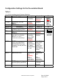
1
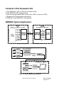
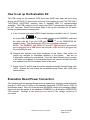
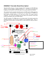
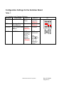
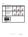
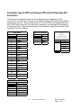
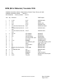
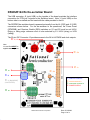
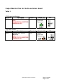
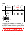
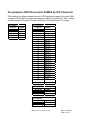
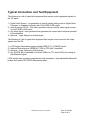
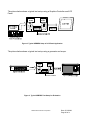
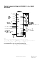
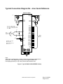
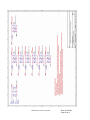
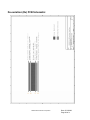
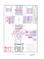
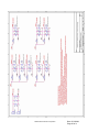
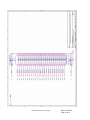
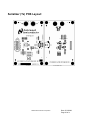
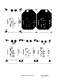
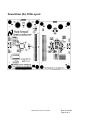
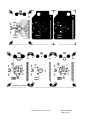
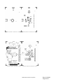
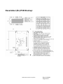
FPD to Serdes (UR) Translator Chip
DS99R421
Evaluation Kit
User’s Manual
NSID: FPDXSDUR-43USB
Rev 0.0
National Semiconductor Corporation
Date: 5/12/2008
Page 1 of 39
Table of Contents
TABLE OF CONTENTS ........................................................................................................................................... 2
INTRODUCTION: ..................................................................................................................................................... 3
CONTENTS OF THE EVALUATION KIT:........................................................................................................... 4
SERDES TYPICAL APPLICATION:...................................................................................................................... 4
HOW TO SET UP THE EVALUATION KIT:........................................................................................................ 6
EVALUATION BOARD POWER CONNECTION: .............................................................................................. 6
DS99R421 TRANSLATOR BOARD DESCRIPTION: .......................................................................................... 7
CONFIGURATION SETTINGS FOR THE SERIALIZER BOARD ......................................................................................... 8
TRANSLATOR INPUT LVDS AND OUTPUT FPD-LINK II PINOUT BY IDC CONNECTOR ........................................... 11
BOM (BILL OF MATERIALS) TRANSLATOR PCB: ................................................................................................... 12
DS90UR124 RX DE-SERIALIZER BOARD:........................................................................................................ 13
CONFIGURATION SETTINGS FOR THE DE-SERIALIZER BOARD ................................................................................. 14
OUTPUT MONITOR PINS FOR THE DE-SERIALIZER BOARD ...................................................................................... 15
DE-SERIALIZER LVDS PINOUT AND LVCMOS BY IDC CONNECTOR .................................................................... 17
BOM (BILL OF MATERIALS) DE-SERIALIZER PCB: ................................................................................................ 18
TYPICAL CONNECTION AND TEST EQUIPMENT........................................................................................ 19
TYPICAL CONNECTION DIAGRAM DS99R421 – USER QUICK REFERENCE........................................ 21
TYPICAL CONNECTION DIAGRAM RX – USER QUICK REFERENCE.................................................... 22
TROUBLESHOOTING ........................................................................................................................................... 23
APPENDIX................................................................................................................................................................ 25
SERIALIZER (TX) PCB SCHEMATIC:............................................................................................................... 25
DE-SERIALIZER (RX) PCB SCHEMATIC:........................................................................................................ 28
SERIALIZER (TX) PCB LAYOUT: ...................................................................................................................... 32
SERIALIZER (TX) PCB STACKUP: .................................................................................................................... 35
DESERIALIZER (RX) PCB LAYOUT:................................................................................................................. 36
DESERIALIZER (RX) PCB STACKUP:............................................................................................................... 39
National Semiconductor Corporation
Date: 5/12/2008
Page 2 of 39
Introduction:
National Semiconductor’s DS99R421 standard multi-channel LVDS to FPD-Link II
translator SERDES evaluation kit contains 1 - DS99R421 translator board and 1 DS90UR124 De-serializer (Rx) board, and 1 - two (2) meter high speed USB 2.0 cable.
Note: the evaluation boards are not for EMI testing. The evaluation boards were
designed for easy accessibility to device pins with tap points for monitoring or applying
signals, additional pads for termination, loading, and multiple connector options.
The DS99R421 and DS90UR124 chipset supports a variety of display and general
purpose applications. The single FPD-Link II interface is well-suited for any display
system interface. Typical applications include: navigation displays, automated teller
machines (ATMs), POS, video cameras, global positioning systems (GPS), portable
equipment/instruments, factory automation, etc.
The DS99R421 can be used to take existing standard multi-channel LVDS and convert
them to a single channel FPD-Link II format. DS99R421 can be used as a 21-bit
general purpose LVDS translator used in conjunction with the DS90UR124 FPD-Link II
De-serializer chipset and transmit data at clocks speeds ranging from 5 to 43 MHz.
The DS99R421 LVDS to FPD-Link II translator board accepts four (4) standard LVDS
multi-channel LVDS input signals and converts them into a single serialized FPD-Link II
data pair with an embedded LVDS clock. The serial data stream toggles at 28 times the
base clock rate with an input clock at up to 43 MHz. The maximum transmission rate
for the FPD-Link II line is 1.204Gbps.
The DS90UR124 de-serializer board accepts the FPD-Link II serialized data stream with
embedded clock and converts the serialized data back into parallel 3.3V_LVCMOS
signals and clock. Note that NO reference clock is needed to prevent harmonic lock.
Suggested equipment to evaluate the chipset are: a standard LVDS signal source such
as a video generator, or FPD or Channel Link or equivalent transmitter and/or word
generator or pulse generator and oscilloscope with a bandwidth of at least 43 MHz will
be needed.
The user needs to provide the standard multi-channel LVDS inputs to the LVDS
translator and also provide a proper interface from the de-serializer output to an LCD
panel or test equipment. The translator and de-serializer boards can also be used to
evaluate device parameters. A cable conversion board or harness scramble may be
necessary depending on type of cable/connector interface used on the input to the
DS99R421 and to the output of the DS90UR124.
Example of suggested display setup:
1) video generator with an 18 bit data LVDS output
2) 18-bit LCD panel with a 3.3V_LVCMOS input interface.
National Semiconductor Corporation
Date: 5/12/2008
Page 3 of 39
Contents of the Evaluation Kit:
1) One DS99R421 LVDS to FPD-Link II translator board
2) One DS90UR124 De-serializer board
3) One 2-meter high speed USB 2.0 cable (4-pin USB A to 5-pin mini USB)
4) Evaluation Kit Documentation (this manual)
5) DS99R421 and DS90UR241/124 Datasheet
SERDES Typical Application:
Figure 1a. Typical Application (18-bit RGB Color)
Figure 1b. Typical SERDES System Diagram
National Semiconductor Corporation
Date: 5/12/2008
Page 4 of 39
Figures 1a and 1b illustrate the use of the chipset (DS99R421/DS90UR124) in a Host to
Flat Panel Interface.
The chipsets support up to 18-bit color depth TFT LCD Panels.
Refer to the proper datasheet information on chipset provided on each board for more
detailed information.
National Semiconductor Corporation
Date: 5/12/2008
Page 5 of 39
How to set up the Evaluation Kit:
The PCB routing for the translator LVDS input pins (RxIN) have been laid out to plug
directly into FPD HSL Tx demo board (note only 6 bit mapping is used). The FPD-Link II
TxOUT/RxIN (DOUT/RIN) interface uses a standard USB 2.0 connector/cable
assembly. The PCB routing for the Rx output pins (ROUT) are accessed through a 50pin IDC connector. Please follow these steps to set up the evaluation kit for bench
testing and performance measurements:
1) A two (2) meter high speed USB 2.0 cable has been included in the kit. Connect
1
2
3
4
A
the 4-pin USB A
side of cable harness to the DS99R421 board and
the other side the 5-pin mini USB jack 1 2 3 4 MIN to the DS90UR124 deserializer board. This completes the FPD-Link II interface connection.
NOTE: The DS99R421 and DS90C124 are NOT USB compliant and should
not be plugged into a USB device nor should a USB device be plugged into
the evaluation boards.
2) Jumpers and switches have been configured at the factory; they should not
require any changes for immediate operation of the chipset.
See text on
Configuration settings for more details. From the Video Decoder board, connect
a flat cable (not supplied) to the translator board and connect another flat cable
(not supplied) from the De-serializer board to the panel.
3) Power for the Tx and Rx boards must be supplied externally through Power Jack
(VDD). Grounds for both boards are connected through Power Jack (VSS) (see
section below).
Evaluation Board Power Connection:
The translator and de-serializer boards must be powered by supplying power externally
through J3 (VDD) and J4 (VSS) on the translator board and J4 (VDD) and J5 (VSS) on
de-serializer board. Note +4V is the absolute MAXIMUM voltage (not operating voltage)
that should ever be applied to the translator (DS99R421) or de-serializer (DS90UR124)
VDD terminal. Damage to the device(s) can result if the voltage maximum is
exceeded.
National Semiconductor Corporation
Date: 5/12/2008
Page 6 of 39
DS99R421 Translator Board Description:
The 20-pin IDC connector J1 accepts standard 18-bit 3-channels of LVDS RGB data
(RxIN0+/-, RxIN1+/-, RxIN2+/-) and clock (RxCLK+/-). The 100 ohm terminations are
integrated in the DS99R421 LVDS RxIN inputs so no external resistors are required.
The translator board is powered externally from the J3 (VDD) and J4 (VSS) connectors
shown below. For the serializer to be operational, the Power Down (S1-PWDNB) and
Data Enable (S1-DEN) switches on S1 must be set HIGH. The board is factory
configured. JP1 and JP2 are configured from the factory to be shorted to VSS; these
are the unused power wires in the cable harness.
The USB connector P2 (USB-A side) on the bottom side of the board provides the
interface connection to the FPD-Link II signals to the De-serializer board. Note: P1
(mini USB) on the top side is un-stuffed and not to be used with the cable provided in
the kit.
Note:
VDD and VSS MUST
be applied externally
from here.
NOT FOR EMI TESTING
f J4, J5
NOT FOR EMI TESTING
h R5
f VR1, JP6
Note:
Connect cable
to P2 on BACKSIDE.
c P2 (BACKSIDE)
J1
d
c P1 (TOPSIDE)
(UNSTUFFED)
e
S1 f
JP7
NOT FOR EMI TESTING
National Semiconductor Corporation
c FPD-Link II OUTPUT
d LVDS INPUTS
e LVCMOS INPUTS
f FUNCTION CONTROLS
g POWER SUPPLY
h 100Ω FPD-Link II OUTPUT
Date: 5/12/2008
Page 7 of 39
Configuration Settings for the Serializer Board
Table 1.
S1: Serializer Input Features Selection
Reference
Description
Input = L
PWDNB
PoWerDowN Bar Powered
Down
DEN
VODSEL
BISTEN
Serializer Output
Data ENabled
LVDS output VOD
SELect
BIST ENabled
Disabled
≈350mV
(Default)
BIST
DISABLED
MUST be
low for
normal
operation
(Default)
Input = H
Normal
operation
(Default)
Enabled
(Default)
≈700mV
S1
BIST
ENABLED.
Note:
DS90UR124
BISTEN MUST
also be set
High. (see
datasheet for
operational
modes)
National Semiconductor Corporation
Date: 5/12/2008
Page 8 of 39
Table 2.
JP6,VR1: Pre-Emphasis Feature Selection
Reference
Description
JP6
Pre-Emphasis – helps to
increase the eye pattern
opening in the LVDS stream
JP6 &
VR1
Pre-Emphasis adjustment
(via screw)
JP6 MUST have a jumper to
use VR1 potentiometer.
VR1 = 0Ω to 20KΩ,
JP6 + VR1 + 6KΩ (R6) =
~6KΩ (maximum preemphasis) to
~26KΩ (minimum preemphasis*).
IPRE = [1.2/(RPRE)] x 40,
RPRE (minimum) > 6KΩ
OPEN
(floating)
Disabled –
no jumper
(Default)
CLOSED
(Path to GND)
Enabled –
With jumper
Clockwise
CounterClockwise
increases
RPRE value
which
decreases
preemphasis
decreases
RPRE value
which
increases
preemphasis
*Note: maximum is based on resistor
value. In this case ~26KΩ value is based
on the ~6kΩ fixed resistor plus ~20KΩ
maximum potentiometer value. User can
use hundreds of Kohms to reduce the preemphasis value.
Pre-emphasis user note:
Pre-emphasis must be adjusted correctly based on application frequency, cable quality,
cable length, and connector quality. Maximum pre-emphasis should only be used under
extreme worse case conditions; for example at the upper frequency specification of the
part and/or low grade cables at maximum cable lengths. Typically all that is needed is
minimum pre-emphasis. Users should start with no pre-emphasis first and gradually
apply pre-emphasis until there is clock lock and no data errors. The best way to monitor
the pre-emphasis effect is to hook up a differential probe to the 100Ω termination
resistor (R1) on the DS90UR124 Rx demo board (NOT to R5 on the DS99R421 demo
board). The reason for monitoring R1 on the Rx side is because you want to see what
the receiver will see the attenuation signal AFTER the cable/connector.
National Semiconductor Corporation
Date: 5/12/2008
Page 9 of 39
Table 3.
JP5, JP8: USB Red and Black wire
Reference
Description
Power wire in USB cable
JP5
thru P2 (and P1 not
mounted) connector
Jumper RED to VSS –
recommended
VDD
VSS
Red wire tied Red wire
to VDD
tied to VSS
(Default)
OPEN
Red wire
floating
(not
recommended)
Black wire
tied to VDD
Black wire
floating
(not
recommended)
Note: Normally VDD in USB application
Power wire in USB cable
thru P2 (and P1 not
mounted) connector
Jumper BLACK to VSS –
recommended
JP8
Black wire
tied to VSS
(Default)
Note: Normally VSS in USB application
top side thru the board view
(mounted on solder side)
P2
pin 3
pin 4
USB A
BLACK WIRE
pin 2
+
_
pin 1
RED WIRE
National Semiconductor Corporation
Date: 5/12/2008
Page 10 of 39
Translator Input LVDS and Output FPD-Link II Pinout by IDC
Connector
The following four tables illustrate how the LVDS inputs are mapped to the IDC
connector J1, the FPD-Link II outputs on the USB-A connector P3, and the mini USB P1
(not mounted) pinouts. There are also three (3) 3.3V_LVCMOS over-sampled bits OS1,
OS2, OS3 (extra unused bits, not required for operation); see datasheet for description
of these bits. Note – labels are also printed on the evaluation boards for both the LVDS
input and FPD-Link II outputs.
LVDS INPUT
J1 pin no.
Symbol
FPD-Link II OUTPUT
P3 pin no.
Symbol
1
2
3
VSS
RxIN0RxIN0+
1
2
3
RED
DOUT+
DOUT-
4
VSS
4
BLK
5
6
7
8
VSS
RxIN1RxIN1+
VSS
9
VSS
10
RxIN2-
11
RxIN2+
12
VSS
13
VSS
14
RxCLKIN-
15
RxCLKIN+
16
VSS
17
VSS
18
NC
19
NC
20
VSS
P1
(topside)
(not mounted)
FPD-Link II OUTPUT
pin no.
name
5
JP2
4
3
2
1
NC
DOUTDOUT+
JP1
OS INPUT (3.3v_LVCMOS)
JP3 pin no. Symbol
1
2
3
4
5
6
OS1
VSS
OS2
VSS
OS3
VSS
National Semiconductor Corporation
Date: 5/12/2008
Page 11 of 39
BOM (Bill of Materials) Translator PCB:
DS99R421 Xlator Bench Board - Board Stackup Revised: Friday, February 29, 2008
DS99R421 Xlator Bench Board
Revision: 1
Bill Of Materials
February 29,2008
18:31:46
Item
Qty
Reference
Part
PCB Footprint
1
2
3
4
5
2
1
1
1
7
0.1uF
22uF
2.2uF
0.1uF
22uF
CAP/HDC-0402
CAP/N
3528-21_EIA
CAP/HDC-1206
CAP/EIA-B 3528-21
6
7
0.1uF
CAP/HDC-0603
7
7
0.01uF
CAP/HDC-0603
8
9
10
11
12
13
14
15
16
17
18
2
1
1
1
1
2
1
1
1
1
7
3-Pin Header
2-Pin Header
2X3-Pin Header
2X10-Pin Header, open
2mm_2X5
BANANA
mini USB 5pin_open
USB A
100 ohm,0402
5.76K
0 Ohm,0402
Header/3P
Header/2P
Header/2X3P
Header/2X10P
CON/HDR-10P-B
CON/BANANA-S
mini_B_USB_surface_mount
USB_TYPE_A_4P
RES/HDC-0402
RES/HDC-0402
RES/HDC-0402
19
20
21
22
23
4
1
1
1
2
C1,C2
C18
C19
C20
C21,C22,C23,C30,C33,C36,
C41
C24,C26,C28,C32,C35,C37,
C40
C25,C27,C29,C31,C34,C38,
C39
JP2,JP1
JP2
JP3
J1
J2
J5,J4
P1
P2
R5
R8
R10,R11,R12,R13,R14,R15,
R16
R18,R20,R21,R23
S1
U1
VR1
X2,X1
10K
SW DIP-4
DS99R421
SVR20K
TP_0402
RES/HDC-0805
DIP-8
36 ld LLP socket
Surface Mount 4mm Square
TP/0402
National Semiconductor Corporation
Date: 5/12/2008
Page 12 of 39
DS90UR124 Rx De-serializer Board:
The USB connector J2 (mini USB) on the topside of the board provides the interface
connection for FPD-Link II signals to the Serializer board. Note: J1 (mini USB) on the
bottom side is un-stuffed and not used with the cable provided in the kit.
The SERDES de-serializer board is powered externally from the J4 (VDD) and J5 (VSS)
connectors shown below. For the de-serializer to be operational, the Power Down
(RPWDNB) and Receiver Enable (REN) switches on S1 and S2 must be set HIGH.
Rising or falling edge reference clock is also selected by S1: HIGH (rising) or LOW
(falling).
The 50 pin IDC Connector J3 provides access to the 24 bit LVCMOS and clock outputs.
f J4, J5
Note:
Vcc and Gnd MUST be
applied externally here
d JP4
d J3
e S1
d JP3
c J2
c FPD-Link II INPUTS
d LVCMOS OUTPUTS
e FUNCTION CONTROLS
f POWER SUPPLY
c J1 (BACKSIDE)
(UNSTUFFED)
e S2
National Semiconductor Corporation
Date: 5/12/2008
Page 13 of 39
Configuration Settings for the De-serializer Board
Table 4.
S1, S2: De-serializer Input Features Selection
Reference
Description
Input = L
RPWDNB PoWerDowN Bar
Power Down
(Disabled)
PTOSEL
RESRVD
Progressive Turn On
SELect
RESeRVeD
Reference
Description
RRFB
Latch input data on Rising
or Falling edge of TCLK
REN
Receiver Output Data
ENabled
BISTEN
BIST ENable
Note: MUST set DS99R421
BISTEN = H. Use in
combination with BISTM pin.
BISTM
BIST Mode
Don’t care if BISTEN=L.
BISTEN MUST be High
(enabled) for this pin to be
functional.
RAOFF
RAndomizer OFF
SLEW
SLEW rate control
for ROUT[23:0] and RCLK
Enabled
(Default)
Don’t care
Input = L
Falling Edge
(Default)
Disabled
Normal
Operating
Mode, BIST
Disabled
(Default)
Per Channel
pass/fail;
RxOUT[23:0]
=H: pass;
RxOUT[23:0]
=H: fail
Randomizer
ON.
(Default)
Input = H
Normal
Operational
(Default)
Disabled
Don’t care
Input = H
Rising Edge
S2
Enabled
(Default)
BIST Mode
Enabled
RxOUT[7:0]:
binary error
counting
mode (up to
255 errors);
RxOUT[23:8]:
normal
operation
Randomizer
OFF.
Note:
DS99R421
RAOFF MUST
also be set Low.
Note:
DS99R421
RAOFF MUST
also be set High.
(Default)
~2X slew rate,
~2X drive
strength
National Semiconductor Corporation
S1
Date: 5/12/2008
Page 14 of 39
Output Monitor Pins for the De-serializer Board
Table 5.
JP3: Output Lock Monitor
Reference
Description
Output = L
LOCK
Receiver PLL LOCK
unlocked
Note:
DO NOT PUT A SHORTING
JUMPER IN JP3.
JP4: PASS Monitor
Reference
Description
Output = L
PASS
Receiver BIST monitor
FAIL
PASS flag
Note:
DO NOT PUT A SHORTING
JUMPER IN JP1.
National Semiconductor Corporation
Output = H
PLL LOCKED
(LED2 will
illuminate)
JP3
Output = H
PASS
(LED1 will
illuminate)
JP4
Date: 5/12/2008
Page 15 of 39
Table 6.
JP1, JP2: USB Red and Black wire
Reference
Description
Power wire in USB cable
JP1
thru J2 (and J1 not
mounted) connector
Jumper RED to VSS –
recommended
VDD
VSS
Red wire tied Red wire
to VDD
tied to VSS
(Default)
OPEN
Red wire
floating
(not
recommended)
Black wire
tied to VDD
Black wire
floating
(not
recommended)
Note: Normally VDD in USB application
JP2
Power wire in USB cable
thru J2 (and J1 not
mounted) connector
Jumper BLACK to VSS –
recommended
Black wire
tied to VSS
(Default)
Note: Normally VSS in USB application
mini USB
pin 1
RED WIRE
pin 2
+
_
pin 3
J2
NO connect
pin 4
pin 5
top side view
(mounted on component side)
BLACK WIRE
The following picture depicts a typical example of the FPD-Link II serial stream. This
snapshot was taken with a differential probe across the 100 ohm termination resistor R1
on the DS90UR124 Rx evaluation board. R1 is the termination resistor to the RxIN +/-.
Note: The scope was triggered, with a separate probe, on TCLK, the input clock into the
DS90UR241 Tx. To view the serial stream correctly, do not trigger on the probe
monitoring the serial stream.
National Semiconductor Corporation
Date: 5/12/2008
Page 16 of 39
De-serializer LVDS Pinout and LVCMOS by IDC Connector
The following two tables illustrate how the LVDS inputs are mapped to the mini USB
connector J2 and the Rx outputs are mapped to the IDC connector J3. Note – labels
are also printed on the demo boards for both the LVDS inputs and TTL outputs.
LVDS INPUT
J2 pin no.
Symbol
1
2
3
4
5
RED
DIN+
DINNC
BLK
TTL OUTPUT
J3 pin no.
1
3
5
7
9
11
13
15
17
19
21
23
25
27
29
31
33
35
37
39
41
43
45
47
49
Symbol
ROUT0
ROUT1
ROUT2
ROUT3
ROUT4
ROUT5
ROUT6
ROUT7
ROUT8
ROUT9
ROUT10
ROUT11
ROUT12
ROUT13
ROUT14
ROUT15
ROUT16
ROUT17
ROUT18
ROUT19
ROUT20
ROUT21
ROUT22
ROUT23
TCLK
all even pins
VSS
TTL OUTPUT
JP3 pin no.
Symbol
1
2
TTL OUTPUT
JP4 pin no.
1
2
LOCK (PLL)
VSS
Symbol
PASS (BIST)
VSS
National Semiconductor Corporation
Date: 5/12/2008
Page 17 of 39
BOM (Bill of Materials) De-serializer PCB:
DS90UR124 Rx USB Demo Board - Board Stackup Revised: Monday, October 23, 2006
DS90UR124 Rx USB Demo Board
Revision: 1
Bill Of Materials
October 23, 2006
Item Qty Reference
Part
______________________________________________
1
2
2
27
3
4
5
6
1
1
1
8
7
8
8
8
9
10
11
12
13
14
15
16
17
18
2
2
1
1
1
2
1
1
1
9
19
20
21
1
1
1
C2,C1
C3,C7,C8,C9,C10,C11,C12,
C13,C14,C15,C16,C17,C18,
C19,C20,C21,C22,C23,C24,
C25,C26,C27,C28,C29,C30,
C31,C42
C4
C5
C6
C32,C33,C34,C41,C47,C50,
C53,C54
C35,C38,C40,C43,C46,C48,
C52,C55
C36,C37,C39,C44,C45,C49,
C51,C56
JP2,JP1
JP4,JP3
J1
J2
J3
J4,J5
LED1
LED2
R1
R2,R3,R4,R34,R35,R36,R37,
R38,R39
S1
S2
U1
PCB Footprint
0.1uF
open0402
CAP/HDC-0402
CAP/HDC-0402
2.2uF
22uF
0.1uF
22uF
3528-21_EIA
CAP/N
CAP/HDC-1206
CAP/EIA-B 3528-21
0.1uF
CAP/HDC-0603
0.01uF
CAP/HDC-0603
3-Pin Header
2-Pin Header_open
mini USB 5pin_open
Hirose GT17H-4P-2H
IDC2X25_Unshrouded
BANANA
0402_orange_LED
0603_green_LED
100 ohm,0402
10K
Header/3P
Header/2P
mini_USB_surface_mount
Hirose GT17H-4P-2H
IDC-50
CON/BANANA-S
0402
0603 (Super Thin)
RES/HDC-0402
RES/HDC-0805
SW DIP-3
SW DIP-6
DS90UR124
DIP-6
DIP-12
64 pin TQFP
National Semiconductor Corporation
Date: 5/12/2008
Page 18 of 39
Typical Connection and Test Equipment
The following is a list of typical test equipment that may be used to generate signals for
the TX inputs:
1) Digital Video Source – for generation of specific display timing such as Digital Video
Processor or Graphics Controller with 18-bit RGB LVDS output.
2) Astro Systems VG-835 - This video generator may be used for video signal sources
for 18-bit RGB LVDS output.
3) Any other signal / video generator that generates the correct input levels as specified
in the datasheet.
4) Optional – Logic Analyzer or Oscilloscope
The following is a list of typical test equipment that may be used to monitor the output
signals from the RX:
1)
2)
3)
4)
LCD Display Panel which supports digital RGB (3.3V_LVCMOS) inputs.
National Semiconductor DS99R421 LVDS to FPD-Link II translator
Optional – Logic Analyzer or Oscilloscope
Any SCOPE with a bandwidth of at least 43MHz for TTL and/or 2GHz for looking at
the differential signal.
LVDS signals may be easily measured with high impedance / high bandwidth differential
probes such as the TEK P6330 differential probes.
National Semiconductor Corporation
Date: 5/12/2008
Page 19 of 39
The picture below shows a typical test set up using a Graphics Controller and LCD
Panel.
Figure 2. Typical SERDES Setup of LCD Panel Application
The picture below shows a typical test set up using a generator and scope.
Figure 3. Typical SERDES Test Setup for Evaluation
National Semiconductor Corporation
Date: 5/12/2008
Page 20 of 39
Typical Connection Diagram DS99R421 – User Quick
Reference
Note:
VDDs can be combined into four (4) groupings as shown (top to bottom):
1-Analog-LVDS, 2-Digital, 3-Analog-FPD-Link II, and 4-Analog-PLL/VCO for best performance.
Absolute minimum grouping should be Analog Power and Digital Power.
Decoupling specified (C1-C8) is the minimum that should be used.
Figure 6. Typical DS90C241 Tx SERDES Hookup
National Semiconductor Corporation
Date: 5/12/2008
Page 21 of 39
Typical Connection Diagram Rx – User Quick Reference
DS90C124 (DES)
3.3V
VDDIR
C5
C6
VDDOR1
VDDOR2
VDDOR3
C7
C9
RIN+
SerialSerial
LVDSII
FPD-Link
Interface
Interface
R1
RINC10
3.3V
RPWDNB
REN
RRFB
RPWDNB = System GPO
REN = High (ON)
RRFB = High (Rising edge)
RESRVD = Low
RESRVD
3.3V
C1
C2
C3
C4
VDDR0
VDDR1
C8
C1 to C8 = 0.1 F to 0.01 F
C9 = 100 nF; 50 WVDC, NPO or X7R
C10 = 100 nF; 50 WVDC, NPO or X7R
R1 = 100
GPO
VDDPR0
VDDPR1
ROUT0
ROUT1
ROUT2
ROUT3
ROUT4
ROUT5
ROUT6
ROUT7
ROUT8
ROUT9
ROUT10
ROUT11
ROUT12
ROUT13
ROUT14
ROUT15
LVCMOS
Parallel
Interface
ROUT16
ROUT17
ROUT18
ROUT19
ROUT20
ROUT21
ROUT22
ROUT23
RCLK
LOCK
Note:
VDDs can be combined into a minimum of four (4) groupings as shown above:
Analog-PLL/VCO, Digital-Logic, Analog-LVDS, Digital-LVCMOS O/P
Decoupling specified (C1-C8) is the minimum that should be used.
Figure 7. Typical DS90C124 Rx SERDES Hookup
National Semiconductor Corporation
Date: 5/12/2008
Page 22 of 39
Troubleshooting
If the demo boards are not performing properly, use the following as a guide for quick
solutions to potential problems. If the problem persists, please contact the local Sales
Representative for assistance.
QUICK CHECKS:
1. Check that Power and Ground are connected to both Tx AND Rx boards.
2. Check the supply voltage (typical 3.3V) and also current draw with both Tx and Rx
boards. The Serializer board should draw about 55-65mA with clock and all data
bits switching at 43MHz, (RPRE=9KΩ). The De-serializer board should draw about
75-85mA with clock and all data bits switching at 43MHz, (minimum ROUT loading).
3. Verify input clock and input data signals meet requirements for VILmin, VILmax,
VIHmin, VIHmax, tset, thold), also verify that data is strobed on the selected
rising/falling (RFB pin) edge of the clock.
4. Check that the Jumpers and Switches are set correctly.
5. Check that the cable is properly connected.
TROUBLESHOOTING CHART
Problem…
There is only the output clock.
There is no output data.
Solution…
Make sure the data is applied to the correct input pin.
Make sure data is valid at the input.
No output data and clock.
Make sure Power is on. Input data and clock are
active and connected correctly.
Power, ground, input data and
input clock are connected
correctly, but no outputs.
The devices are pulling more
than 1A of current.
After powering up the demo
boards, the power supply
reads less than 3V when it is
set to 3.3V.
Make sure that the cable is secured to both demo
boards.
Check the Power Down pins of both Translator and
De-serializer boards to make sure that the devices
are enabled (/PD=Vcc) for operation. Also check
DEN on the Serializer board and REN on the
Deserializer board is set HIGH.
Check for shorts in the cables connecting the
Translator and RX boards.
Use a larger power supply that will provide enough
current for the demo boards, a 500mA minimum
power supply is recommended.
National Semiconductor Corporation
Date: 5/12/2008
Page 23 of 39
Note: Please note that the following references are supplied only as a courtesy to our
valued customers. It is not intended to be an endorsement of any particular equipment
or hardware supplier.
Connector References
Hirose Electric Europe B.V.
Beech Avenue 46
1119 PV Schiphol-Rijk
The Netherlands
Phone: +31 20 655 7467, Fax: +31 20 655 7469
www.HiroseEurope.com
Cable References
Nissei Electric Co., LTD
1509 Okubo-Cho, Hamamatsu-City
Shizuoka-Pref, 432-8006 Japan
Phone: +81 53 485 4114, Fax: +81 53 485 6908
www.nissei-el.co.jp
Cable Recommendations
- For optimal performance, we recommend Shielded Twisted Pair (STP) 100Ω
differential impedance cable for high-speed data applications.
Equipment References
Astro Systems
425 S. Victory Blvd. Suite A
Burbank, CA 91502
Phone: (818) 848-7722 , Fax: (818) 848-7799
www.astro-systems.com
Digital Video Pattern Generator – Astro Systems VG-835 (or equivalent):
Extra Component References
TDK Corporation of America
1740 Technology Drive, Suite 510
San Jose, CA 95110
Phone: (408) 437-9585, Fax: (408) 437-9591
www.component.tdk.com
Optional EMI Filters – TDK Chip Beads (or equivalent)
National Semiconductor Corporation
Date: 5/12/2008
Page 24 of 39
Appendix
Serializer (Tx) PCB Schematic:
National Semiconductor Corporation
Date: 5/12/2008
Page 25 of 39
National Semiconductor Corporation
Date: 5/12/2008
Page 26 of 39
National Semiconductor Corporation
Date: 5/12/2008
Page 27 of 39
De-serializer (Rx) PCB Schematic:
National Semiconductor Corporation
Date: 5/12/2008
Page 28 of 39
National Semiconductor Corporation
Date: 5/12/2008
Page 29 of 39
National Semiconductor Corporation
Date: 5/12/2008
Page 30 of 39
National Semiconductor Corporation
Date: 5/12/2008
Page 31 of 39
Serializer (Tx) PCB Layout:
TOP VIEW
BOTTOMSIDE VIEW
National Semiconductor Corporation
Date: 5/12/2008
Page 32 of 39
PRIMARY COMPONENT SIDE – LAYER 1
SECONDARY COMP SIDE – LAYER 4
GROUND PLANE (VSS) – LAYER 2
PRIMARY COMP SIDE – SOLDER MASK (LAYER 1)
National Semiconductor Corporation
POWER PLANE (VDD) – LAYER 3
SECONDARY COMP SIDE – SOLDER MASK (LAYER 4)
Date: 5/12/2008
Page 33 of 39
PRIMARY COMP SIDE – SOLDER PASTE (LAYER 1)
SECONDARY COMP SIDE – SOLDER PASTE (LAYER 4)
SILKSCREEN COMP SIDE – SILKSCREEN (LAYER 4)
National Semiconductor Corporation
Date: 5/12/2008
Page 34 of 39
Serializer (Tx) PCB Stackup:
National Semiconductor Corporation
Date: 5/12/2008
Page 35 of 39
Deserializer (Rx) PCB Layout:
TOP VIEW
BOTTOMSIDE VIEW
National Semiconductor Corporation
Date: 5/12/2008
Page 36 of 39
PRIMARY COMPONENT SIDE – LAYER 1
GROUND PLANE (VSS) – LAYER 2
SECONDARY COMP SIDE – LAYER 4
PRIMARY COMP SIDE – SOLDER MASK (LAYER 1)
National Semiconductor Corporation
POWER PLANE (VDD) – LAYER 3
SECONDARY COMP SIDE – SOLDER MASK (LAYER 4)
Date: 5/12/2008
Page 37 of 39
PRIMARY COMP SIDE – SOLDER PASTE (LAYER 1)
PRIMARY COMP SIDE – SILKSCREEN (LAYER 1)
SECONDARY COMP SIDE – SOLDER PASTE (LAYER 4)
SILKSCREEN COMP SIDE – SILKSCREEN (LAYER 4)
National Semiconductor Corporation
Date: 5/12/2008
Page 38 of 39
Deserializer (Rx) PCB Stackup:
National Semiconductor Corporation
Date: 5/12/2008
Page 39 of 39
IMPORTANT NOTICE
Texas Instruments Incorporated and its subsidiaries (TI) reserve the right to make corrections, modifications, enhancements, improvements,
and other changes to its products and services at any time and to discontinue any product or service without notice. Customers should
obtain the latest relevant information before placing orders and should verify that such information is current and complete. All products are
sold subject to TI’s terms and conditions of sale supplied at the time of order acknowledgment.
TI warrants performance of its hardware products to the specifications applicable at the time of sale in accordance with TI’s standard
warranty. Testing and other quality control techniques are used to the extent TI deems necessary to support this warranty. Except where
mandated by government requirements, testing of all parameters of each product is not necessarily performed.
TI assumes no liability for applications assistance or customer product design. Customers are responsible for their products and
applications using TI components. To minimize the risks associated with customer products and applications, customers should provide
adequate design and operating safeguards.
TI does not warrant or represent that any license, either express or implied, is granted under any TI patent right, copyright, mask work right,
or other TI intellectual property right relating to any combination, machine, or process in which TI products or services are used. Information
published by TI regarding third-party products or services does not constitute a license from TI to use such products or services or a
warranty or endorsement thereof. Use of such information may require a license from a third party under the patents or other intellectual
property of the third party, or a license from TI under the patents or other intellectual property of TI.
Reproduction of TI information in TI data books or data sheets is permissible only if reproduction is without alteration and is accompanied
by all associated warranties, conditions, limitations, and notices. Reproduction of this information with alteration is an unfair and deceptive
business practice. TI is not responsible or liable for such altered documentation. Information of third parties may be subject to additional
restrictions.
Resale of TI products or services with statements different from or beyond the parameters stated by TI for that product or service voids all
express and any implied warranties for the associated TI product or service and is an unfair and deceptive business practice. TI is not
responsible or liable for any such statements.
TI products are not authorized for use in safety-critical applications (such as life support) where a failure of the TI product would reasonably
be expected to cause severe personal injury or death, unless officers of the parties have executed an agreement specifically governing
such use. Buyers represent that they have all necessary expertise in the safety and regulatory ramifications of their applications, and
acknowledge and agree that they are solely responsible for all legal, regulatory and safety-related requirements concerning their products
and any use of TI products in such safety-critical applications, notwithstanding any applications-related information or support that may be
provided by TI. Further, Buyers must fully indemnify TI and its representatives against any damages arising out of the use of TI products in
such safety-critical applications.
TI products are neither designed nor intended for use in military/aerospace applications or environments unless the TI products are
specifically designated by TI as military-grade or "enhanced plastic." Only products designated by TI as military-grade meet military
specifications. Buyers acknowledge and agree that any such use of TI products which TI has not designated as military-grade is solely at
the Buyer's risk, and that they are solely responsible for compliance with all legal and regulatory requirements in connection with such use.
TI products are neither designed nor intended for use in automotive applications or environments unless the specific TI products are
designated by TI as compliant with ISO/TS 16949 requirements. Buyers acknowledge and agree that, if they use any non-designated
products in automotive applications, TI will not be responsible for any failure to meet such requirements.
Following are URLs where you can obtain information on other Texas Instruments products and application solutions:
Products
Applications
Audio
www.ti.com/audio
Automotive and Transportation www.ti.com/automotive
Amplifiers
amplifier.ti.com
Communications and Telecom www.ti.com/communications
Data Converters
dataconverter.ti.com
Computers and Peripherals
www.ti.com/computers
DLP® Products
www.dlp.com
Consumer Electronics
www.ti.com/consumer-apps
DSP
dsp.ti.com
Energy and Lighting
www.ti.com/energy
Clocks and Timers
www.ti.com/clocks
Industrial
www.ti.com/industrial
Interface
interface.ti.com
Medical
www.ti.com/medical
Logic
logic.ti.com
Security
www.ti.com/security
Power Mgmt
power.ti.com
Space, Avionics and Defense
www.ti.com/space-avionics-defense
Microcontrollers
microcontroller.ti.com
Video and Imaging
www.ti.com/video
RFID
www.ti-rfid.com
OMAP Mobile Processors
www.ti.com/omap
Wireless Connectivity
www.ti.com/wirelessconnectivity
TI E2E Community Home Page
e2e.ti.com
Mailing Address: Texas Instruments, Post Office Box 655303, Dallas, Texas 75265
Copyright © 2012, Texas Instruments Incorporated