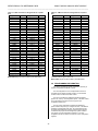
1
Series PMC341 PCI Mezzanine Card Simultaneous Sampling Analog Input Module USER’S MANUAL ACROMAG INCORPORATED 30765 South Wixom Road P.O. BOX 437 Wixom, MI 48393-7037 U.S.A. Tel: (248) 295-0310 Fax: (248) 624-9234 Copyright 2004, Acromag, Inc., Printed in the USA. Data and specifications are subject to change without notice. 8500-654-D13C010 SERIES PMC341 PCI MEZZANINE CARD SIMULTANEOUS ANALOG INPUT MODULE ___________________________________________________________________________________________ The information contained in this manual is subject to change without notice. Acromag, Inc. makes no warranty of any kind with regard to this material, including, but not limited to, the implied warranties of merchantability and fitness for a particular purpose. Further, Acromag, Inc. assumes no responsibility for any errors that may appear in this manual and makes no commitment to update, or keep current, the information contained in this manual. No part of this manual may be copied or reproduced in any form, without the prior written consent of Acromag, Inc. Table of Contents 1.0 GENERAL INFORMATION........................................... KEY PMC341 FEATURES............................................ PCI MEZZANINE CARD INTERFACE FEATURES....... SIGNAL INTERFACE PRODUCTS............................... PMC MODULE ActiveX CONTROL SOFTWARE........ PMC MODULE VxWORKS SOFTWARE…….............. 2.0 PREPARATION FOR USE............................................ UNPACKING AND INSPECTION.................................. CARD CAGE CONSIDERATIONS................................ BOARD CONFIGURATION........................................... Software Configuration…….……............................ CONNECTORS………….............................................. Front Panel Field I/O Connector ……........................ Rear J4 Field I/O Connector………………………….. Analog Inputs: Noise and Grounding Considerations. External Trigger Input/Output.................................... PMC Local Bus Connector ……................................ 3.0 PROGRAMMING INFORMATION................................. PCI Configuration Address Space............................. Configuration Registers............................................. MEMORY MAP…………………..................................... Interrupt Register…………………….……………… Control Register………………………………..…..….. Channel Enable Control Register………...........…..... Low Bank Timer Register……………………….….. High Bank Timer Register…..…………………….….. Memory Threshold Register…………………….…..… Start Convert Register………………………….…..…. Memory Buffer………………………………….…..…. Analog Input & Corresponding Digital Codes……..… Reference Voltage Access Register......................…. Reference Voltage Read Data/Status Register........ MODES OF CONVERSION.......…...........…........ Single Conversion Mode………..…………..…..…. Continuous Conversion Mode….………….......…….. PROGRAMMING CONSIDERATIONS…...........….... Single Conversion Mode Example……………..…... Continuous Conversion Mode with Interrupt Example USE OF CALIBRATION REFERENCE SIGNAL.....…... Uncalibrated Performance…………….................…... Calibrated Performance……………………………..... Calibrated Programming Example…...........…...….. Programming Interrupts ……………...........……...….. 4.0 THEORY OF OPERATION............................................ FIELD ANALOG INPUTS.............................................. LOGIC/POWER INTERFACE....................................... PCI INTERFACE LOGIC............................................... BURST READ OF PMC341 MEMORY.......................... CONVERSION CONTROL LOGIC…………….…… MULTIPLEXER CONTROL CIRCUITRY………….….. DATA TRANSFER FROM ADC TO FPGA............…..... CONVERSION COUNTER………........….............…..... MEMORY BUFFER SWITCH CONTROL...................... EXTERNAL TRIGGER.………................................…... INTERRUPT CONTROL LOGIC…......................…...... REFERENCE VOLTAGE MEMORY CONTROL LOGIC. Page 2 3 3 3 3 4 4 4 4 4 4 4 4 5 5 5 5 6 7 7 7 7 8 9 9 9 10 10 10 10 11 11 11 11 12 12 12 12 13 13 13 13 14 14 14 15 15 16 16 16 16 16 16 16 16 16 -2- 5.0 SERVICE AND REPAIR................................................ SERVICE AND REPAIR ASSISTANCE........................ PRELIMINARY SERVICE PROCEDURE...................... 17 17 17 6.0 SPECIFICATIONS......................................................... PHYSICAL…………………...............................…......... ENVIRONMENTAL………………………………..….. ANALOG INPUT....….................................................... PCI Local Bus Interface..………………......................... 17 17 17 18 19 APPENDIX.................................................................... CABLE, SCSI-2 to Flat Ribbon (Shielded): MODEL 5028-187……….............................................. TERMINATION PANEL: MODEL 5025-552................... 19 19 DRAWINGS 4501-844 PMC MECHANICAL ASSEMBLY................. 4501-878 PMC341 BLOCK DIAGRAM......................... 4501-879 ANALOG INPUT CONNECTION.................. 4501-758 CABLE, SCSI-2 to Flat Ribbon (Shielded) 5028-187…………………….............................. 4501-464 TERMINATION PANEL 5025-552................ Page 20 21 22 23 19 24 IMPORTANT SAFETY CONSIDERATIONS It is very important for the user to consider the possible adverse effects of power, wiring, component, sensor, or software failures in designing any type of control or monitoring system. This is especially important where economic property loss or human life is involved. It is important that the user employ satisfactory overall system design. It is agreed between the Buyer and Acromag, that this is the Buyer's responsibility. Trademarks are the property of their respective owners. 1.0 GENERAL INFORMATION The PCI Mezzanine Card (PMC) Series PMC341 (14-bit) module is a precision, single size PMC module with simultaneous sampling of analog input signals. Sixteen differential analog input channels are provided with an input range of 10 volts. The 16 differential analog voltage input channels are converted as two banks of eight channels. After the first bank of eight channels are simultaneously converted, the second bank of 8 channels can then be simultaneously converted at the time specified in a user programmable delay counter. All 16-channels share two generous 512-sample memory buffers, from which digitized values are read. Since all channels share the same memory buffer, data tagging is implemented for easy identification of corresponding channel data. To minimize CPU interaction, interrupt generation is also supported upon reaching a programmable memory full threshold condition. The PMC341 utilizes state of the art Surface-Mounted Technology (SMT) to achieve its wide functionality and is an ideal choice for a wide range of industrial and scientific applications that require, high-performance analog inputs. SERIES PMC341 PCI MEZZANINE CARD SIMULTANEOUS ANALOG INPUT MODULE ___________________________________________________________________________________________ The PMC341 modules are available in standard or extended temperature range as follows: Model Resolution 512 Sample Temperature Memory Buffer Range PMC341 14-bit Yes 0 to +70C PMC341E 14-bit Yes -40 to +85C PMC341R 14-bit Yes 0 to +70C PMC341RE 14-bit Yes -40 to +85C Note: PMC341R and PMC341RE are rear field I/O models, only. All other models have front I/O. KEY PMC341 FEATURES to a single PMC341 timer reference. As an input the signal will trigger the PMC341 hardware to initiate data conversions. Precision On Board Calibration Voltages - Calibration autozero and autospan precision voltages are available to permit host computer correction of conversion errors. The calibration voltages can be converted and then compared to the expected value stored in on board memory. Calibration voltages include: 0V (local analog ground), and a precision 5 volt reference. Fault Protected Input Channels - Analog input overvoltage protection to +/-25V with power on and +/-40V with power off. PCI MEZZANINE CARD INTERFACE FEATURES 14-Bit ADC Resolution - Eight individual 14-bit successive approximation Analog to Digital Converters (ADC) with integral sample and hold are utilized. 8sec Conversion Time - A maximum conversion rate of 125KHz is supported. Two 512 Sample Memory Buffers – Two 512 sample deep memory buffers are available to reduce CPU interactions. While new digitized data is written to one memory buffer, data can be read from the other at burst data rates. This allows the external processor to service more tasks within a given time. Data tagging is also implemented for easy channel data identification. Memory Buffers Switch Condition – When the number of new data samples exceed a programmable threshold value the input buffer switches to the data read buffer which allows reading of the new data. The old read buffer will simultaneously switch from the data read to the data input buffer. Interrupt Upon Reaching a Memory Threshold Condition – An interrupt can be generated when the number of new data samples reaches a programmable threshold condition. This feature can be used to minimize CPU interaction. Programmable Control of Channels Converted - Up to 16 differential analog inputs are monitored. Channels 0 to 7 are simultaneously converted followed by the simultaneous conversion of channels 8 to 15. Channels may be individually enabled/disabled for simultaneous conversion. User Programmable Conversion Timer - A programmable conversion timer is available to control the time between simultaneous conversion of new banks of channel data. For example, channels 0-7 are converted immediately upon trigger and then channels 8-15 are converted after a user programmable delay from the start of the first eight channels. An overall count value is also used to control when conversions will start again for the first eight channels. Supports a maximum interval of 2.09 seconds. Continuous Conversion Mode - All channels selected for conversion are continually digitized with the interval between conversions controlled by the user programmed conversion timer registers. Scanning is initiated by a software or external trigger. Scanning is stopped by software control. Single Cycle Conversion Mode - All channels selected for conversion are digitized once with the time between channels 0 to 7 and 8 to 15 controlled by a programmable timer. Single cycle conversion mode is initiated by a software or external trigger. External Trigger Input or Output - The external trigger is assigned to a field I/O line. This external trigger may be configured as an input, output, or disabled. As an output this signal provides a means to synchronize other modules High density - Single-width PMC Target module. Field Connections – All analog input, trigger, and power connections are made through a single 50-pin SCSI-2 front panel I/O connector. Models PMC341R and PMC341RE, only use a 64 pin rear I/O connector. 32, 16, 8-bit I/O - Register Read/Write is performed through data transfer cycles in the PCI memory space. All registers can be assessed via 32, 16, or 8-bit data transfers. Compatibility – IEEE P1386.1 compliant PMC module which complies to PCI Local Bus Specification Revision 2.2. Provides one multifunction interrupt. 5V signaling compliant and 3.3V signaling tolerant. SIGNAL INTERFACE PRODUCTS (See Appendix for more information on compatible products) This PMC Module will mate directly to any standard PMC carrier board that supports one single width PMC mezzanine module. Once connected, the module is accessed via a 50 pin front panel connector. The cables and termination panels, described in the following paragraphs, are also available. For optimum performance with the PMC341 analog input module, use of the shortest possible length of shielded input cable is recommended. Cables: Model 5025-187 (SCSI-2 to Flat Ribbon Cable, Shielded): A round 50 conductor shielded cable with a male SCSI-2 connector at one end and a flat female ribbon connector at the other end. The cable is used for connecting the PMC341 module to Model 5025-552 termination panels. Termination Panel: Model 5025-552: DIN-rail mountable panel provides 50 screw terminals for universal field I/O termination. Connects to Acromag PMC341, via SCSI-2 to Flat Ribbon Cable, Shielded (Model 5028-187). PMC MODULE ActiveX CONTROL SOFTWARE Acromag provides a software product (sold separately) consisting of PMC module ActiveX (Object Linking and Embedding) drivers for Windows 98, 95, ME, 2000 and Windows NT compatible application programs (Model PMCSWATX, MSDOS format). This software provides individual drivers that allow Acromag PMC modules to be easily integrated into Windows application programs, such as Visual C++, Visual Basic, Microsoft Office 97 applications and others. The ActiveX controls provide a high-level interface to PMC modules, -3- SERIES PMC341 PCI MEZZANINE CARD SIMULTANEOUS ANALOG INPUT MODULE ___________________________________________________________________________________________ eliminating the need to perform low-level reads/writes of registers, and the writing of interrupt handlers—all the complicated details of programming are handled by the ActiveX controls. These functions consist of an ActiveX control for each Acromag PMC module. industrial environment and the board is exposed to environmental air, careful consideration should be given to air-filtering. BOARD CONFIGURATION Power should be removed from the carrier/CPU board when installing PMC modules, cables, termination panels, and field wiring. Refer to Mechanical Assembly Drawing 4501-844 and the following discussion for configuration and assembly instructions. PMC MODULE VxWORKS SOFTWARE Acromag provides a software product (sold separately) consisting of PMC module VxWorks drivers. This software (Model PMCSW-API-VXW MSDOS format) is composed of VxWorks (real time operating system) libraries for all Acromag PMC modules. The software is implemented as a library of “C” functions which link with existing user code to make possible simple control of all Acromag PMC modules. Software Configuration Software configurable control registers are provided for control of external trigger mode, conversion mode, timer control, channel enable, and interrupt mode selection. No hardware jumpers are required for control of these functions. These control registers must also be configured as needed for the application before starting analog input conversions. Refer to section 3 for programming details. 2.0 PREPARATION FOR USE UNPACKING AND INSPECTION CONNECTORS Upon receipt of this product, Inspect the shipping carton for evidence of mishandling during transit. If the shipping carton is badly damaged or water stained, request that the carrier's agent be present when the carton is opened. If the carrier's agent is absent when the carton is opened and the contents of the carton are damaged, keep the carton and packing material for the agent's inspection. Connectors of the PMC341 modules consist of one 50-pin front panel SCSI-2 field I/O connector, and two 64 pin PCI local bus connectors. These interface connectors are discussed in the following sections. Front Panel Field I/O Connector The front panel connector provides the field I/O interface connections. The front panel connector is a SCSI-2 50-pin female connector (AMP 787082-5 or equivalent) employing latch blocks and 30 micron gold in the mating area (per MIL-G-45204, Type II, Grade C). Connects to Acromag termination panel 5025552 from the front panel via round shielded cable (Model 5028187). For repairs to a product damaged in shipment, refer to the Acromag Service Policy to obtain return instructions. It is suggested that salvageable shipping cartons and packing material be saved for future use in the event the product must be shipped. This board is physically protected with packing material and electrically protected with an anti-static bag during shipment. However, it is recommended that the board be visually inspected for evidence of mishandling prior to applying power. Front panel connector pin assignments are shown in Table 2.1. When reading Table 2.1 and 2.2, note that channel designations are abbreviated to save space. . For example, channel 0 is abbreviated as “+CH00” & “-CH00” for the + & connections, respectively. Table 2.1: PMC341 Front Field I/O Pin Connections Pin Description Number Pin Description Number +CH00 1 -CH08 26 -CH00 2 COMMON 27 COMMON 3 +CH09 28 +CH01 4 -CH09 29 -CH01 5 COMMON 30 COMMON 6 +CH10 31 +CH02 7 -CH10 32 -CH02 8 COMMON 33 COMMON 9 +CH11 34 +CH03 10 -CH11 35 -CH03 11 COMMON 36 COMMON 12 +CH12 37 +CH04 13 -CH12 38 -CH04 14 COMMON 39 COMMON 15 +CH13 40 +CH05 16 -CH13 41 -CH05 17 COMMON 42 COMMON 18 +CH14 43 +CH06 19 -CH14 44 -CH06 20 COMMON 45 COMMON 21 +CH15 46 The board utilizes static sensitive components and should only be handled at a static-safe workstation. CARD CAGE CONSIDERATIONS Refer to the specifications for loading and power requirements. Be sure that the system power supplies are able to accommodate the power requirements of the carrier board, plus the installed PMC modules, within the voltage tolerances specified. IMPORTANT: Adequate air circulation must be provided to prevent a temperature rise above the maximum operating temperature. The dense packing of the PMC module to the carrier/CPU board restricts air flow within the card cage and is cause for concern. Adequate air circulation must be provided to prevent a temperature rise above the maximum operating temperature and to prolong the life of the electronics. If the installation is in an -4- SERIES PMC341 PCI MEZZANINE CARD SIMULTANEOUS ANALOG INPUT MODULE ___________________________________________________________________________________________ +CH07 22 -CH15 -CH07 23 COMMON COMMON 24 EXT TRIGGER* +CH08 25 SHIELD * Indicates that the signal is active low. Rear J4 Field I/O Connector 47 48 49 50 The PMC341 is non-isolated, since there is electrical continuity between the logic and field I/O grounds. As such, the field I/O connections are not isolated from the carrier/CPU board and backplane. Care should be taken in designing installations without isolation to avoid noise pickup and ground loops caused by multiple ground connections. This is particularly important for analog inputs when a high level of accuracy/resolution is needed. The rear J4 connector provides the field I/O interface connections. The rear connector is a 64-pin female receptacle header (AMP 120527-1 or equivalent). Rear field I/O connector pin assignments are shown in Table 2.2. External Trigger Input/Output The external trigger signal on pin 49 of the front panel connector can be programmed as an input, output, or disabled. Table 2.2: PMC341R Rear Field I/O Pin Connections (J4) Pin Description Number Pin Description Number +CH00 1 COMMON 33 -CH00 2 +CH11 34 COMMON 3 -CH11 35 +CH01 4 COMMON 36 -CH01 5 +CH12 37 COMMON 6 -CH12 38 +CH02 7 COMMON 39 -CH02 8 +CH13 40 COMMON 9 -CH13 41 +CH03 10 COMMON 42 -CH03 11 +CH14 43 COMMON 12 -CH14 44 +CH04 13 COMMON 45 -CH04 14 +CH15 46 COMMON 15 -CH15 47 +CH05 16 COMMON 48 -CH05 17 EXT TRIGGER* 49 COMMON 18 COMMON 50 +CH06 19 COMMON 51 -CH06 20 COMMON 52 COMMON 21 COMMON 53 +CH07 22 COMMON 54 -CH07 23 COMMON 55 COMMON 24 COMMON 56 +CH08 25 COMMON 57 -CH08 26 COMMON 58 COMMON 27 COMMON 59 +CH09 28 COMMON 60 -CH09 29 COMMON 61 COMMON 30 COMMON 62 +CH10 31 COMMON 63 -CH10 32 SHIELD 64 * Indicates that the signal is active low. As an input, the external trigger must be a 5 Volt logic, TTLcompatible, debounced signal referenced to analog common. The external trigger signal is an active low edge sensitive signal. That is, the external trigger signal will trigger the PMC341 hardware on the falling edge. Once the external trigger signal has been driven low, it should remain low for a minimum of 500 nano seconds. As an output an active-low TTL signal can be driven to additional PMC341s, thus providing a means to synchronize the conversions of multiple PMC341s. The additional PMC341s must program their external trigger for signal input and convert on external trigger only mode. See section 3.0 for programming details to make use of this signal. The external trigger signal can also be disabled. This prevents external noise from falsely triggering the module. See section 3.0 for programming details to make use of this signal. PMC Local Bus Connector The PMC341 module provides a 32-bit PCI interface to the carrier via two 64 pin connectors. These connectors are 64-pin female receptacle header (AMP 120527-1 or equivalent) which mates to the male connector of the carrier board (AMP 120521-1 or equivalent). This provides excellent connection integrity and utilizes gold-plating in the mating area. Threaded metric screws and spacers are supplied with the PMC module to provide additional stability for harsh environments (see Drawing 4501-844 for assembly details). The pin assignments of PCI local bus connector are standard for all PMC modules according to the PCI Mezzanine Card Specification (see Table 2.3 and 2.4). Analog Inputs: Noise and Grounding Considerations Differential inputs require two leads (+ and -) per channel, and provide rejection of common mode voltages. This allows the desired signal to be accurately measured. However, the signal being measured cannot be floating--it must be referenced to analog common on the PMC module and be within the normal input voltage range. Differential inputs are the best choice when the input channels are sourced from different locations having slightly different ground references and when minimizing noise and maximizing accuracy are key concerns. See Drawing 4501-879 for analog input connections for differential-ended inputs. Shielded cable of the shortest length possible is also strongly recommended. -5- SERIES PMC341 PCI MEZZANINE CARD SIMULTANEOUS ANALOG INPUT MODULE ___________________________________________________________________________________________ Table 2.4: PMC Connector Pin Assignments for J2 (32-bit PCI) Signal Name Pin # Signal Name Pin # +12V 1 TRST# 2 TMS 3 TDO 4 TDI 5 GND 6 GND 7 PCI-RSVD* 8 PCI-RSVD* 9 PCI-RSVD* 10 BUSMODE2# 11 +3.3V 12 RST# 13 BUSMODE3# 14 +3.3V 15 BUSMODE4# 16 PCI-RSVD* 17 GND 18 AD[30] 19 AD[29] 20 GND 21 AD[26] 22 AD[24] 23 +3.3V 24 IDSEL 25 AD[23] 26 +3.3V 27 AD[20] 28 AD[18] 29 +GND 30 AD[16] 31 C/BE[2]# 32 GND 33 PCI-RSVD 34 TRDY# 35 +3.3V 36 GND 37 STOP# 38 PERR# 39 GND 40 +3.3V 41 SERR# 42 C/BE[1]# 43 GND 44 AD[14] 45 AD[13] 46 GND 47 AD[10] 48 AD[08] 49 +3.3V 50 AD[07] 51 PCI-RSVD 52 +3.3V 53 PCI-RSVD 54 PCI-RSVD 55 GND 56 PCI-RSVD 57 PCI-RSVD 58 GND 59 PCI-RSVD 60 ACK64# 61 +3.3V 62 GND 63 PCI-RSVD 64 Table 2.3: PMC Connector Pin Assignments for J1 (32-bit PCI) Signal Name Pin # Signal Name Pin # TCK 1 -12V 2 GND 3 INTA# 4 INTB# 5 INTC# 6 BUSMODE1# 7 +5V 8 INTD# 9 PCI-RSVD* 10 GND 11 PCI-RSVD* 12 CLK 13 GND 14 GND 15 GNT# 16 REQ# 17 +5V 18 V(I/O) 19 AD[31] 20 AD[28] 21 AD[27] 22 AD[25] 23 GND 24 GND 25 C/BE[3]# 26 AD[22] 27 AD[21] 28 AD[19] 29 +5V 30 V(I/O) 31 AD[17] 32 FRAME# 33 GND 34 GND 35 IRDY# 36 DEVSEL# 37 +5V 38 GND 39 LOCK# 40 SDONE# 41 SBO# 42 PAR 43 GND 44 V(I/O) 45 AD[15] 46 AD[12] 47 AD[11] 48 AD[09] 49 +5V 50 GND 51 C/BE[0]# 52 AD[06] 53 AD[05] 54 AD[04] 55 GND 56 V(I/O) 57 AD[03] 58 AD[02] 59 AD[01] 60 AD[00] 61 +5V 62 GND 63 REQ64# 64 # Indicates that the signal is active low. BOLD ITALIC Signals are NOT USED by this PMC Model. # Indicates that the signal is active low. BOLD ITALIC Signals are NOT USED by this PMC Model. 3.0 PROGRAMMING INFORMATION This Section provides the specific information necessary to program and operate the PMC341 module. This Acromag PMC341 is a PCI Specification version 2.2 compliant PCI bus target only PMC module. The carrier/CPU connects a PCI host bus to the PMC module. The PCI bus is defined to address three distinct address spaces: I/O, memory, and configuration space. The PMC module can be accessed via the PCI bus memory space and configuration spaces only. The PCI card’s configuration registers are initialized by system software at power-up to configure the card. The PMC341 module is a Plug-and-Play PCI card. As a Plug-and-Play card the board’s base address and system interrupt request line are not selected via jumpers but are assigned by system software upon power-up via the configuration registers. A PCI bus configuration access is used to access a PCI card’s configuration registers. -6- SERIES PMC341 PCI MEZZANINE CARD SIMULTANEOUS ANALOG INPUT MODULE ___________________________________________________________________________________________ PCI Configuration Address Space Table 3.2: PMC341 Memory Map2 Base D31 D15 Addr+ D16 D00 03 Not Used1 Interrupt Register When the computer is first powered-up, the computer’s system configuration software scans the PCI bus to determine what PCI devices are present. The software also determines the configuration requirements of the PCI card. Base Addr+ 00 07 The system software accesses the configuration registers to determine how many blocks of memory space the carrier requires. It then programs the PMC module’s configuration registers with the unique memory base address. Control Register 04 0B Not Used1 0F Channel Enable Control Low Bank Timer 13 High Bank Timer 08 0C The configuration registers are also used to indicate that the PMC module requires an interrupt request line. The system software then programs the configuration registers with the interrupt request line assigned to the PMC module. 10 17 Since this PMC module is relocatable and not fixed in address space, this module’s device driver must use the mapping information stored in the module’s Configuration Space registers to determine where the module is mapped in memory space and which interrupt line will be used. 1B Configuration Registers 27 1F 23 The PCI specification requires software driven initialization and configuration via the Configuration Address space. This PMC module provides 256 bytes of configuration registers for this purpose. The PMC341 contains the configuration registers, shown in Table 3.1, to facilitate Plug-and-Play compatibility. 29 7FF 803 The Configuration Registers are accessed via the Configuration Address and Data Ports. The most important Configuration Registers are the Base Address Registers and the Interrupt Line Register which must be read to determine the base address assigned to the PMC341 and the interrupt request line that goes active on a PMC341 interrupt request. FFF Not Used1 Memory Threshold Register Not Used Start Convert Bits-31 to 01 Bit-0 Not Used1 Reference Voltage Access Register Not Used1 Reference Voltage Data & Status Not Used1 Reference Voltage Write Enable Code3 Not Used1 Not Used1 1st Memory Location Not Used(31:20), Tag bits(19:16), Data(15:0) 512th Memory Location Not Used(31:20), Tag bits(19:16), Data(15:0) 14 18 1C 20 24 28 7FC 800 FFC Notes (Table 3.2): 1. The PMC341 will return 0 for all addresses that are "Not Used". 2. All Reads and writes are 8 clock cycles. 3. This byte is reserved for use at the factory to enable writing of the reference voltage. Write only byte value = “A3”. Table 3.1 Configuration Registers Reg. D31 D24 D23 D16 D15 D7 Num. D8 D0 Device ID=4D4D Vendor ID= 16D5 0 Status Command 1 Class Code=118000 Rev ID=00 2 BIST Header Latency Cache 3 32-bit Memory Base Address for PMC341 4 4K-Byte Block Not Used 5 : 10 Subsystem ID=0000 Subsystem Vendor 11 ID=0000 Not Used 12 Reserved 13,14 Max_Lat Min_Gnt Inter. Pin Inter. Line 15 This memory map reflects byte accesses using the “Little Endian” byte ordering format. Little Endian uses even-byte addresses to store the low-order byte. The Intel x86 family of microprocessors uses “Little Endian” byte ordering. Big Endian is the convention used in the Motorola 68000 microprocessor family and is the VMEbus convention. In Big Endian, the lower-order byte is stored at odd-byte addresses. Interrupt Register, (Read/Write) - (Base + 00H) This read/write register is used to enable board interrupt, determine the pending status of interrupts, and release an interrupt. MEMORY MAP This board is allocated a 4K byte block of memory that is addressable in the PCI bus memory space to control the acquisition of analog inputs from the field. As such, three types of information are stored in the memory space: control, status, and data. The function of each of the interrupt register bits are described in Table 3.3. This register can be read or written with either 8-bit, 16-bit, or 32-bit data transfers. A power-up or system reset sets all interrupt register bits to 0. The memory space address map for the PMC341 is shown in Table 3.2. Note that the base address for the PMC341 in memory space must be added to the addresses shown to properly access the PMC341 registers. Register accesses as 32, 16, and 8-bit in memory space are permitted. -7- SERIES PMC341 PCI MEZZANINE CARD SIMULTANEOUS ANALOG INPUT MODULE ___________________________________________________________________________________________ Table 3.3: Interrupt Register BIT FUNCTION 0 Board Interrupt Enable Bit. (Read/Write Bit) 0 = Disable Interrupt 1 = Enable Interrupt If enabled via this bit an interrupt request from the module will be issued to the system if the Memory contains more than the threshold number of bytes selected via the Memory Threshold register. The interrupt request will remain active until the interrupt release bit is set, or by disabling interrupts via this bit. 1 Board Interrupt Pending Status Bit. (Read Only Bit) 0 = Interrupt Not Pending 1 = Interrupt Pending This bit can be read to determine the interrupt pending status of the PMC341. When this bit is logic “1” an interrupt is pending and will cause an interrupt request if bit-0 of the register is set. When this bit is a logic “0” an interrupt is not being requested. This bit will only indicate a pending status if the board is enabled for interrupt via bit-0. Once the bit is in the pending status it will remain until the pending interrupt is removed even if interrupts are disabled via bit-0. 14 to 2 Not Used1 15 Board Interrupt Release Bit. (Write Only Bit) 0 = Interrupt Not Released 1 = Interrupt Released This bit must be set to a logic “1” to release an interrupt request. This bit is typically set in the interrupt service routine to remove the interrupt request. Once an interrupt request is generated on the PMC341, it will continue to assert the interrupt request until this Interrupt Release bit is set to logic “1” or interrupts are disabled via bit-0 of this register. BIT 3, 2 (Read/ Write Bits) 5, 4 (Read/ Write Bits) 6 (Read/ Write Bit) Notes (Table 3.3): 1. All bits labeled “Not Used” will return logic “0” when read. Control Register, (Read/Write) - (Base + 04H) This read/write register is used to enable single or continuous conversions, select conversion of calibration voltages or field analog signals, control external trigger input/output mode, monitor Memory status, and issue a software reset to the module. 7 8 (Read Only Bit) The function of each control register bit is described in Table 3.4. This register can be read or written via 8-bit, 16-bit, or 32-bit data transfers. A power-up or system reset sets all control register bits to 0. Table 3.4: Control Register BIT FUNCTION 00 = Conversions are disabled. 1, 0 01 = Enable Single Conversion Mode. A single (Read/ conversion is initiated per software start Write convert or external trigger. The internal Bits) channel timer controls the start conversion of channels 8-15. 10 = Enable Continuous Conversion Mode. Conversions are initiated by a software start convert or external trigger and continued by 14-9 15 (Write Only Bit) FUNCTION internal hardware triggers generated at the frequency set by the interval timer registers. 11 = Reserved 00 = All Channels Differential Input. 01 = Auto Zero Calibration Voltage Input. 10 = Auto Span Calibration Voltage. 11 = Reserved 00 = 01 = 10 = 11 = External Trigger Disable. External Trigger Set as Input. External Trigger Set as Output. Reserved. As an output Internal Timer triggers are driven on the External trigger pin of the field I/O connector. The External Trigger output signal can be used to synchronize the conversion of multiple modules. A single master PMC341 must be selected for External Trigger output and Continuous Conversion mode while all other modules are selected for External Trigger input and Single Conversion mode. The external trigger signals (pin 49 of the field I/O) must be wired together for all synchronized modules. Also, the High Bank Timer must be programmed with the same value on all synchronized modules. The external trigger initiates conversion of the Lower Bank while conversion of the High Bank is controlled by the High Bank Conversion Timer. The External Trigger input can be sensitive to external EMI noise which can cause erroneous external triggers. If External Trigger input or output is not required, the External Trigger should be configured as Disabled. 0 = Enable Continued Analog Input 1 = Disable Conversions on Memory Bank Switch If the system cannot read all valid data values available in the memory buffer before the rate of new input data acquisition causes the buffers to switch, then the automatic disabling of analog input acquisition upon memory bank switching can be selected via this control register bit. If this bit is set to 1, analog input will be disabled upon a memory bank switch. Also, bits 0 and 1 of this register will be set to 00 to reflect the disabled analog input mode. Not Used Transition Status Bit 1 = Valid Data in Memory 0 = Waiting for New Valid Data in Memory This transition status bit can be polled to insure the Memory buffer data is valid. The transition status bit will be set when the memory buffer switches causing new valid data to be available in the read memory buffer. The transition status bit is cleared upon the first read of the memory buffer and will not be set again until new valid data is available. Not Used 0 = Software Reset Inactive. 1 = Software Reset Issued. Reset signal is held active for 300ns. Notes (Table 3.4): 1. All bits labeled “Not Used” will return logic “0” when read. -8- SERIES PMC341 PCI MEZZANINE CARD SIMULTANEOUS ANALOG INPUT MODULE ___________________________________________________________________________________________ Figure1: Time line of channel bank conversions The software reset will clear this control register, the channel enable register, counters, and the Memory Threshold register. The 24-bit Low Bank Timer value divides an 8 MHz clock signal. The output of this Low Bank Timer is used to precisely generate periodic trigger pulses to control the frequency at which all enabled channels are converted. The time period between trigger pulses is described by the following equation: Channel Enable Control Register (Read/Write, 08H) The Channel Enable Control register (bits-15 to 0) is used to select the channels desired for conversion. Only those channels enabled are stored into the data Memory buffer. When the channel’s corresponding bit is set high, per the table below, the channel’s converted data is tagged and stored into the Memory buffer. For example, to enable channels 15, 11, and 7 through 0 the Channel Enable register must be set as 88FF hex. Low Bank T imerValue + 1 The following equation can be used to calculate the Low Bank Timer value. Note, this gives the value in decimal. It must still be converted to hex before it is written to the Low Bank Timer register. Low Bank TimerValue = (T seconds 8,000,000Hz) - 1 Reading or writing to this register is possible via 32-bit, 16-bit or 8-bit data transfers. This register’s contents are cleared upon reset. Where: T = the desired time period between trigger pulses in seconds. Low Bank Timer Value can be a minimum of 63 decimal if only channels 0 to 7 are enabled for conversion. If any channels in the upper bank (channels 8 to 15) are also enabled, then the minimum value is 127 decimal. The maximum value is 16,777,214 decimal. Channel Enable Control Register MSB 15 Ch15 MSB 07 Ch7 14 Ch14 13 Ch13 12 Ch12 11 Ch11 10 Ch10 09 Ch09 06 Ch6 05 Ch5 04 Ch4 03 Ch3 02 Ch2 01 Ch1 LSB 08 Ch08 LSB 00 Ch0 The maximum period of time which can be programmed to occur between simultaneous conversions is (16,777,214 + 1) 8,000,000 = 2.097151875 seconds. The minimum time interval which can be programmed to occur is (63 + 1) 8,000,000 = 8.0 seconds. This minimum of 8.0 seconds is defined by the minimum conversion time of the hardware given only channels 0 to 7 are enabled for conversions. If any of channels 8 to 15 are enabled for conversion, then the minimum time that the Low Bank Timer can be programmed is 127 decimal. The minimum time of 16 seconds allows 8 seconds for channels 0 to 7 and 8 seconds for channels 8 to 15. Low Bank Timer Register (Read/Write, 0CH) Timed periodic triggering can be used to achieve precise time intervals between conversions. The Low Bank Timer register is a 24 bit register value that controls the interval time between conversions of all enabled channels. The Low Bank Timer is used to control the frequency at which the conversion cycle is repeated for all enabled channels. For example, upon software or external trigger, channels 0 to 7 are simultaneously converted. The time programmed into the High Bank Timer Register then determines when channels 8 to 15 are simultaneously converted. The cycle repeats when the time programmed into Low Bank Timer has lapsed. At this time, channels 0 to 7 will again be simultaneously converted. Thus, the Low Bank Timer value must always be greater than the High Bank Timer value by at least 8 seconds. If Continuous Conversions are selected via the Control register, then conversions will continue until disabled. See figure 1 for an illustration of the sequence of conversions described in this paragraph. t1= 8us min t1= 8us min CH8-15 CH0-7 t0 t1 t2 0us Time of initial software or external trigger The 8 seconds maximum sample rate corresponds to a maximum sample frequency of 125KHz. The maximum analog input frequency should be band limited to one half the sample frequency. An anti-aliasing filter should be added to remove unwanted signals above 1/2 the sample frequency in the input signal for critical applications. Reading or writing the Low Bank Timer register is possible with 32-bit, 16-bit or 8-bit data transfers. This register’s contents are cleared upon reset. High Bank Timer Register (Read/Write, 10H) The conversion cycle repeats CH0-7 = T in seconds 8,000,000Hz The High Bank Timer register is a 24 bit register that controls when the upper bank of channels 8 to 15 are converted. time The High Bank Timer is used to control the delay after channels 0 to 7 are converted until channels 8 to 15 are simultaneously converted. For example, upon software or external trigger channels 0 to 7 are simultaneously converted. Then, the time programmed into this counter determines when channels 8 to 15 will be simultaneously converted. See figure 1 for an illustration of this sequence of events. Min time= 8us Min time = 8us + t1 min High Bank Low Bank Timer Value Timer Value Where: High Bank Timer Value must be 8 seconds Low Bank Timer Value must be t1 + 8 seconds If a channel within the 8 to 15 bank is enabled in the Channel Enable Control register, then the High Bank Timer register must -9- SERIES PMC341 PCI MEZZANINE CARD SIMULTANEOUS ANALOG INPUT MODULE ___________________________________________________________________________________________ be programmed with a delay. If this register is left as zero erroneous operation will result. Start Convert Register (Write Only, 18H) The 24-bit High Bank Timer value is divided by an 8 MHz clock signal. The output of this Timer is used to precisely generate periodic trigger pulses to control the frequency at which the bank of channels 8 to 15 are simultaneously converted. The time period between trigger pulses is described by the following equation: High Bank Timer Value + 1 8,000,000 Hz The Start Convert register is write-only and is used to trigger conversions by setting data bit-0 to a logic one. This method of starting conversions is most useful for its simplicity and for when precise time of conversion is not critical. Typically, software triggering is used for initiating the first conversion. The PMC341 control and timer register bits must first be configured before the Start Convert bit is set. = T in seconds This register can be written via 32-bit, 16-bit or 8-bit data transfer. Data bit-0 must be a logic one to initiate data conversions. Where: T = the desired time period between trigger pulses in seconds. The High Bank Timer Value can be minimum of 63 decimal. The maximum value is 16,777,150 decimal. The maximum period of time which can be programmed to occur between conversions is (16,777,150 + 1) 8,000,000 = 2.097143875 seconds. The minimum time interval which can be programmed to occur is (63 + 1) 8,000,000 = 8.0 seconds. This minimum of 8.0 seconds is defined by the minimum conversion time of the hardware. This gives channels 0 to 7 eight micro seconds to complete their simultaneous conversion. Then, channels 8 to 15 can be simultaneously converted. 31 Start Convert Register Not Used 01 Start Convert 00 Memory Buffer (Read Only, 800H to FFCH) In order to support burst data acquisition of digitized converted data, two 512-sample memory buffers are used. While one buffer functions to acquire new data input from the converters, the other functions as a read buffer. Data can be read at burst rates via the PCI bus to obtain new digitized data. The two memory buffers switch functions based upon the Memory Threshold register value, when the number of new input digitized data samples exceeds the Memory Threshold value. Reading or writing the High Bank Timer register is possible with 32-bit, 16-bit or 8-bit data transfers. This register’s contents are cleared upon reset. Memory Threshold Register (Read/Write, 14H) Since all channels share the same memory, channel data tagging is implemented. The tag value identifies the channel to which the data corresponds. The hardware tags each memory location with a channel number, so the data can easily match with its source channel. The Memory Threshold register is an 8-bit register that is used to control transition between two 512 deep memory banks. One memory bank is used to store converted analog input data while the other is accessible for reading of converted analog input data. When the analog input memory buffer contains more samples than the Memory Threshold value the memory banks will switch. This allows software to read the new converted analog input data. The new data must be read before the memory banks switch again. If the system cannot keep up by reading the memory buffer before they switch, then the automatic disabling of analog input upon memory bank switching can be selected via the control register bit-6. The Memory samples are 20-bit data values. The least significant bits, 15 to 0, represent the digitized data while bits 19 to 16 represent the channel tag. Care should be taken when reading data from the memory buffer. To insure the memory buffer data is valid the Transition Status bit (bit-8 of the Control Register) can be polled. The Transition Status bit will be set when valid data is available in the memory buffer. The Transition Status bit is cleared upon the first read of the memory buffer and will not be set again until the memory buffers switch, based upon the Threshold register value. Alternatively, an interrupt upon threshold met condition can be used to start reading of valid data. The number of valid analog input data samples available in the memory buffer will be one more than the value set in the Memory Threshold register. Thus, if the memory threshold value is 33 then 34 valid data entries will be present in memory when the memory buffer switch occurs. The Memory Threshold register value can be any value between 1 and 511. Reading of the Memory is possible via 32-bit, 16-bit, or 8-bit data transfers. An interrupt can also be issued upon exceeding the specified threshold level, if enabled via bit-0 of the interrupt register. This interrupt indicates that new data is available in the memory buffer. An interrupt request can be released by setting bit-15 of the Interrupt register to a logic one. The interrupt request can also be disabled by setting bit-0 to a logic zero; however, the interrupt request will remain active on the PMC341 until released via bit-15. Analog Input and Corresponding Digital Codes The data coding is in binary two’s compliment. The digital code corresponding to each of the given ideal analog input values is given in binary two’s complement format in Table 3.5. Note that the 14 bit data values are left justified within the 16-bit word. For the PMC341 the least significant 2 bits will be returned as zero when read. Reading or writing to this register is possible via 32-bit, 16-bit or 8-bit data transfers. This register’s contents are set to 1FF hex (511 decimal) upon reset. - 10 - SERIES PMC341 PCI MEZZANINE CARD SIMULTANEOUS ANALOG INPUT MODULE ___________________________________________________________________________________________ Table 3.5: Digital Output Codes and Input Voltages DESCRIPTION ANALOG INPUT Model PMC341 (14-bit) Least Significant Bit Weight 1.22mV + Full Scale 9.998779 7FFC Minus One LSB Volts hex Midscale 0V 0000h One LSB Below -1.22mV FFFC Midscale hex Minus Full Scale -10V 8000 hex Write accesses to the Reference Voltage Access register are possible via 32-bit or 16-bit data transfers, only. Storing the reference voltage value to memory is normally only performed at the factory. A software or hardware reset has no affect on this register. Reference Voltage Read Data/Status Register (Read, 20H) The Reference Voltage Read Data/Status register is a readonly register and is used to access the read data and determine the status of a read cycle initiated by the Reference Voltage Access register. In addition, this register is used to determine the status of a write cycle to the memory. When bit-1 of this register is set it indicates the memory is busy completing a write cycle. Reference Voltage Access Register (Write, 1CH) This register is used to initiate a read of the reference voltage value. The reference voltage value is provided so that software can adjust and improve the accuracy of the analog input voltage over the uncalibrated state. The reference voltage is precisely measured at the factory and then stored to this location at the addresses given in table 3.6. All read accesses to this Data/Status register initiate an approximately 1millisecond access to the memory. Thus, you must wait 1 millisecond after reading this Data/Status register before a new read or write cycle to the memory can be initiated, (an EEPROM latency limitation). A read request, initiated through the Reference Voltage Access register, will provide the addressed digit of the reference voltage on data bits 15 to 8 of the Reference Voltage Data/Status register. Although the read request via the Reference Voltage Access register is accomplished in 200 nano seconds, typically, the reference voltage digit will not be available in the Reference Voltage Data/Status register for approximately 2.5 milliseconds. The Reference Voltage Access Register is a write-only register and is used to configure and initiate a read cycle to the Reference Voltage memory. Setting bit-15 of this register high, to a “1’’, initiates a read cycle. Setting bit-15 of this register low, to a “0’’, initiates a write cycle. The address of the Reference Voltage to be read must be specified on bits 14 to 8 of the Reference Voltage Access register. Read or Write~ 15 Bit-0 of the Reference Voltage Data/Status register is the read complete status bit. This bit will be set high to indicate that the requested reference voltage digit is available on data bits 15 to 8 of the Reference Voltage Data/Status register. This bit is cleared upon initiation of a new read access of the memory or upon issue of a hardware reset. Reference Voltage Access Register Address Write Data 14, 13, 12, 11, 10, 9, 8 7 down to 0 Reference Voltage Read Data/Status Register Read Data Not Used Write Read Busy Complete 15 Down to 8 7 Down to 2 1 0 The reference voltage is stored in memory as a null terminated ASCII character string. For example if the value 4.99835 were stored to memory the corresponding ASCII characters would be 34, 2E, 39, 39, 38, 33, 35, 00 as shown in Table 3.6. Note, the ASCII equivalent of a decimal point is 2E and the null character is 00. The memory should be read starting at address 00 until the null ASCII character is read. This string can then be converted into a float by using your compiler’s ATOF function. Table 3.6: Reference Voltage Address Memory Map Address (Hex) 00 01 02 03 04 05 06 Example Reference Value 4 . 9 9 8 3 5 ASCII Characters As Stored In Memory 34 2E 39 39 38 33 35 Writes to Reference Voltage memory require a special enable code and are normally only performed at the factory. The module should be returned to Acromag if the reference voltage must be re-measured and stored to memory. A write operation to the memory, initiated via the Reference Voltage Access register, will take approximately 5 milliseconds. Bit-1 of the Reference Voltage Data/Status register serves as a write operation busy status indicator. Bit-1 will be set high upon initiation of a write operation and will remain high until the requested write operation has completed. New read or write accesses to the memory, via the Reference Voltage Access register, should not be initiated unless the write busy status bit-1 is clear (set low to 0). A hardware reset of the IP module will also clear this bit. 07 null 00 The address corresponding to each of the reference voltage digits is given in hex. The most significant digit is stored at address 00 hex. Read accesses to the Reference Voltage Data/Status register are possible via 32-bit or 16-bit data transfers, only. A software or hardware reset will clear all bits to zero. For additional details on the use of the reference voltage, refer to the “Data Correction” section. - 11 - SERIES PMC341 PCI MEZZANINE CARD SIMULTANEOUS ANALOG INPUT MODULE ___________________________________________________________________________________________ MODES OF CONVERSION set when valid data is available in the memory buffer. The Transition Status bit is cleared upon the first read of the memory buffer and will not be set again until the memory buffers switch again based upon the Threshold register value. The PMC341 provides two methods of analog input operation for maximum flexibility with different applications. The following sections describe the features of each method and how to best use them. PROGRAMMING CONSIDERATIONS Single Conversion Mode The PMC341 provides different methods of analog input acquisition to give the user maximum flexibility for their application. Examples are presented in the following sections to illustrate programming the different modes of operation. In the Single Conversion mode, conversions are initiated by a software or external trigger. Upon the trigger, channels 0 to 7 will be simultaneously converted. Then, after the time programmed into the High Bank Timer has been reached, channels 8 to 15 will be converted. All channels enabled in the Channel Enable Control register will be tagged with their channel number and stored to the memory buffer. No additional conversions will be initiated unless a new software or external trigger is generated. Single Conversion Mode Example This example will enable channels 0, 3, and 8 through 15 for the single conversion mode of operation. Conversions can be initiated via software or external trigger. Channels 8 to 15 will be simultaneously converted 16 seconds after channels 0 and 3. To select this mode of operation bits 1 and 0 of the Channel Control register must be set to digital code “01”. Then, issuing a software start convert or external trigger will initiate conversions. The Low Bank Timer is not used in this mode of operation. Also, the High Bank Timer is not needed if channels 8 to 15 are disabled. 1. Execute Write of 0011H to the Control Register at Base Address + 04H. a) Single Conversion is enabled. b) External and Software generated triggers are enabled. This mode of operation can be used to initiate conversions based on external triggers. This can be used to synchronize multiple modules to a single module running in a continuous conversion mode. The external trigger of a PMC341 “master” must be programmed as an output. The external trigger signal of that module must then be connected to the external trigger signal of all other modules that are to be synchronized. These other modules must be programmed for Single Conversion mode and external trigger input. Also, the High Bank Timer must be programmed with the same value on all synchronized modules. Note that the external trigger only initiates the conversion of the Low Bank. The conversion of the High Bank is controlled by use of the High Bank Timer. 2. Execute Write of FF09H to the Channel Enable Control register at Base Address + 08H. This will enable channels 0, 3, and 8 through 15 for conversion. 3. Execute Write of 007FH to the High Bank Timer at Base Address + 10H. Channels 8 to 15 will be converted 16 seconds after channels 0, and 3. 4. Execute Write of 0001H to the Start Convert Bit at Base Address + 18H. This starts the simultaneous conversion of channels 3 and 0. Then, 16 seconds later, channels 8 to 15 are simultaneously converted. Continuous Conversion Mode with Interrupt Example Data conversion can be initiated via the Start Convert bit of the master module configured for continuous conversion mode. This example will enable channels 0 through 13 for the continuous conversion mode of operation. Interrupts are enabled and an interrupt threshold of 430 samples is programmed. The Low Bank Timer will be set for an 80 second interval. The High Bank Timer is set to activate the simultaneous conversion of channels 8 through 13 at 23 seconds after channels 0 to 7. Conversions can be initiated via software or external trigger. Continuous Conversion Mode In the Continuous Conversion mode, the hardware controls the continuous conversions of all enabled channels. All channels 0 to 15 are converted at the rate specified by the Low Bank Timer. Channels, 8 to 15, are converted after channels 0 to 7. The time programmed into the High Bank Timer specifies how long after channels 0 to 7 are converted before channels 8 to 15 are converted. 1. Enable interrupts for the PMC module by writing a “1” to bit 1 of the Interrupt Register at Base Address + 00H. 2. Execute Write of 0012H to the Control Register at Base Address + 04H. a) Continuous Conversion mode is selected. b) External and Software generated triggers are enabled. To initiate this mode bits 1 and 0 of the Channel Control register must be set to digital code “10”. Then, issuing a software start convert or external trigger will initiate the continuous conversions of all enabled channels. 3. Execute Write of 3FFFH to the Channel Enable Control register at Base Address + 08H. This will enable channels 0 through 13 for conversion. The interrupt capability of the module can be employed as a means to indicate to the system that up to 512 samples (depending on the threshold selected via the Threshold register) are available to be read. 4. Execute Write of 027FH to the Low Bank Timer Register at Base Address + 0CH. a) This sets the Conversion Timer to 639 decimal as needed for an 80 second interval. Alternatively, a polling method could be used. The Transition Status bit (bit-8 of the Control Register) can be polled to insure the memory buffer data is valid. The Transition Status bit will be - 12 - SERIES PMC341 PCI MEZZANINE CARD SIMULTANEOUS ANALOG INPUT MODULE ___________________________________________________________________________________________ 5. Execute Write of 00B7H to the High Bank Timer Register at Base Address + 10H. a) This sets the High Bank Timer to 183 decimal as needed for a 23 seconds delay after channels 0 through 7. Note: (183+1) 8,000,000 = 23 seconds. Equation (1) following is used to correct the actual ADC data (i.e. the uncorrected bit count read from the ADC) making use of the stored reference voltage. CorrectValue = CountRead Count 6. Execute Write of 1AEH to the Memory Threshold register at Base Address + 14H. a) The PMC341 will issue an interrupt to the system when more than 430 samples are present in the Memory buffer. 7. Execute Write of 0001H to the Start Convert Bit at Base Address + 18H. a) This starts the simultaneous conversion of channels 0 to 7. Then, after 23 seconds channels 8 through 13 are simultaneously converted. The cycle repeats every 80 seconds. Where: Count5V = Count0V = CountRead = 0V (1) Count 5V Count 0V 5VRefValue Actual ADC Data Read With 5 Volt Calibration Voltage Applied Actual ADC Data Read With Auto Zero Calibration Voltage Applied Uncorrected ADC Data Read For Channel Undergoing Correction. The 5VRefValue represents the five volt reference value as it is read from stored memory via the Reference Voltage Access register and the Reference Voltage Read Data/Status register. The Count5V and Count0V reference voltages should not be determined immediately after startup but after the module has reached a stable temperature (about 20 minutes) and updated periodically (e.g. once an hour, or more often if ambient temperatures change) to obtain the best accuracy. Note that several readings (e.g. 100) of the reference voltages should be taken via the ADC and averaged to reduce the measurement uncertainty, since these points are critical to the overall system accuracy. USE OF CALIBRATION REFERENCE SIGNAL A Reference voltage signal for analog input calibration has been provided for use to improve the accuracy over the uncalibrated state. The use of software calibration allows the elimination of hardware calibration potentiometers traditionally used in precision analog front ends. Software calibration uses some fairly complex equations. Acromag recommends purchase of our ActiveX or VxWorks software to make communication with the board and calibration easy. It relieves you from having to turn the equations in the following sections into debugged software calibration code. Calibration Programming Example Assume that channels 0 through 3 are enabled, and corrected input channel data is desired. The calibration parameters (Count5V and Count0V) need to be determined for channels 0 through 3 before the analog field signals can be corrected. Note that channel 0 and 8 share the same INAMP and ADC and thus share the same Count5V and Count0V values. This is also true for channels 1 and 9, 2 and 10, etc.. Uncalibrated Performance The uncalibrated performance is affected by two primary error sources. These are the Instrumentation Amplifier (IN-AMP) and the Analog to Digital Converter (ADC). The untrimmed INAMP and ADC have significant offset and gain errors (see specifications in chapter 6) which reveal the need for software calibration. Determination of the Count0V Value Calibrated Performance 1. Execute Write of 01H to the Interrupt Register at Base Address + 00H. a) Interrupts Enabled 2. Execute Write of 0046H to the Control Register at Base Address + 04H. a) Continuous Mode Enabled b) Auto Zero Calibration Voltage Selected (Count0V) c) External Trigger Disabled d) Analog Input is Disabled on Memory Bank Switch 3. Execute Write of 000FH to the Channel Enable Control Register at Base Address + 08H. This will permit the Auto Zero values corresponding to channels 0 to 3 to be stored in the memory buffer. 4. Execute Write of BFH to the Low Bank Timer register at Base Address + 0CH. This sets the interval time between conversions to 24 seconds. 5. Execute Write of 18FH to the Memory Threshold register at Base Address + 14H. Since interrupts are Very accurate calibration of the PMC341 can be accomplished by using the calibration reference voltage and auto zero (analog ground reference) present on the board. The five volt and the analog ground references are used to determine two points of a straight line which defines the analog input characteristic. The exact value of the five volt reference is stored in on board memory to provide the most accurate calibration. The PMC341 has eight separate ADC circuits. As such, each of the first eight channels will have their own unique offset and gain errors. Note, channels 8 through 15 share the gain and offset values of channels 0 through 7. The five volt reference (Auto Span Calibration Voltage) and the ground reference (Auto Zero voltage) will need to be selected and converted through each of the eight channels to determine the corrected value as given in equation 1. - 13 - SERIES PMC341 PCI MEZZANINE CARD SIMULTANEOUS ANALOG INPUT MODULE ___________________________________________________________________________________________ enabled in the control register, an interrupt request will be issued when 400 values of the Auto Zero calibration voltage have been stored in the memory buffer. This corresponds to 100 values for each of the four channels enabled. 6. Execute Write of 0001H to the Start Convert Bit at Base Address + 18H. This starts the continuous mode of conversions. 7. Upon system interrupt, Analog input is disabled as requested via bit-6 of the Control register. Execute Write of 8000H to the Interrupt Register at Base Address + 00H. a) Interrupts are disabled, and the Interrupt request is released. 8. Software must read the memory buffer and calculate a Count0V value for each channel 0 to 3, by averaging the 100 values for each channel. Read the Reference Voltage Value From Memory 15. To initiate a read of the second memory location of the reference voltage value, the Reference Voltage Access register must be written with data value 8100H at Base Address + 1CH. When bit 0 of the Calibration Coefficient Status register is set to logic high, then the data on bits 15 to 8 of this register contains the decimal point digit of the reference voltage value. Determination of the Count5V Value 9. 10. 11. Execute Write of 01H to the Interrupt Register at Base Address + 00H. a) Interrupts Enabled 16. 13. Upon system interrupt, Analog input is disabled as requested via bit-6 of the Control register. Execute Write of 8000H to the Interrupt Register at Base Address + 00H. a) Interrupts are disabled, and the Interrupt request is released. Since Count0V, Count5V, and 5VRefValue are known, corrected input data values can now be determined. Start Conversion Of Differential Input Channel Data Writing the Channel Enable register, Low Bank Timer Value, and the Memory Threshold is not necessary because they need not change from that programmed in the previous steps. Execute Write of 0001H to the Start Convert Bit at Base Address + 18H. This starts the continuous mode of conversions. 14. This procedure must continue until the null ASCII character is read from memory. The string can then be converted into a float by using your compiler’s ATOF function. Execute Write of 004AH to the Control Register at Base Address + 04H. a) Continuous Mode Enabled b) Auto Span Calibration Voltage Selected (Count5V) c) External Trigger Disabled d) Analog Input is Disabled on Memory Bank Switch 12. Read the reference voltage memory to retrieve the unique reference voltage value (5VRefValue). To obtain the reference voltage value the ASCII characters comprising the reference voltage must be read until the null (terminating) character “00” is read. To read the most significant digit, the Reference Voltage Access register must be written with data value 8000H at Base Address + 1CH. The data can be read by polling the Reference Voltage Read Data/Status register. When bit 0 of the Reference Voltage Read Data/Status register is set to logic high, then the data on bits 15 to 8 contains the most significant digit of the reference voltage value, represented as an ASCII character. Software must read the memory buffer and calculate a Count5V value for each channel 0 to 3, by averaging the 100 values for each channel. 17. Execute Write of 01H to the Interrupt Register at Base Address + 00H. a) Interrupts Enabled 18. Execute Write of 0042H to Control Register at Base Address + 04H. a) Continuous Mode Enabled b) Channel Differential Input Selected c) External Trigger Disabled d) Analog Input is Disabled on Memory Bank Switch 19. Execute Write 0001H to the Start Convert Bit at Base Address + 18H. This starts the continuous mode of conversions. Continuous simultaneous conversions of channels 0 to 3 are implemented and corresponding results are stored in the Memory buffer. 20. Upon system interrupt the Memory buffer at Base Address + 800H must be read. The data read should be corrected per equation 1 of this section. Programming Interrupts Interrupts can be enabled for generation after the Memory buffer contains more new data values than that set by the Memory Threshold register. Interrupts generated by the PMC341 use interrupt request line INTA# . The interrupt release mechanism is release on register access. That is, the PMC341 will release the INTA# signal when bit-15 of the Interrupt Register at Base Address + 00H is set to logic “1”. - 14 - SERIES PMC341 PCI MEZZANINE CARD SIMULTANEOUS ANALOG INPUT MODULE ___________________________________________________________________________________________ Analog inputs and calibration voltages are selected via analog multiplexers. PMC module control logic drives the select signals of the multiplexer as required per the programming of the control register. Interrupt Programming Example 1. 2. 3. Enable PMC341 board interrupt by writing a “1” to bit 0 of the Interrupt register at Base Address + 00H. Set the Memory Threshold register as desired at Base Address + 14H. Interrupts can now be generated after more samples than that set in the Memory Threshold register are available in the Memory buffer. Up to 16 differential inputs can be monitored. The multiplexer stage directs one of two groups of eight channels for simultaneous conversion. Channels 0 to 7 are simultaneously selected and converted by eight individual ADC’s, and channels 8 to 15 are also simultaneously converted. General Sequence of Events for Processing an Interrupt 1. 2. 3. 4. 5. 6. 7. 8. 9. The output of the multiplexer stage feeds an instrumentation amplifier (INAMP) stage. The INAMP has a fixed gain of one. The INAMPs high input impedance allows measurement of analog input signals without loading the source. The INAMP takes in the channel’s + and - inputs and outputs a single ended voltage proportional to it. The PMC341 asserts the Interrupt Request Line (INTA#) in response to an interrupt condition. Determine the IRQ line assigned to the PMC341 during system configuration (read configuration register number 15). Set up the system interrupt vector for the appropriate interrupt. Unmask the IRQ in the system interrupt controller. The interrupt service routine pointed to by the vector set up in step 3 starts. Interrupt service routine determines if the PMC341 has a pending interrupt request by reading the Interrupt pending bit-1 of the Interrupt register. Example of Generic Interrupt Handler Actions: a) Disable the interrupting PMC341 by writing “0” to bit-0 of the Interrupt Register to disable interrupts on the PMC341. b) Service the interrupt by reading converted data resident in the Memory buffer of the PMC341. c) Clear the interrupt request by writing a “1” to bit-15 of the Interrupt register. d) Enable the PMC341 for interrupts by writing “1” to bit-0 of the Interrupt register. Write “End-Of-Interrupt” command to systems interrupt controller. If the PMC341’s interrupt stimulus has been removed, the interrupt cycle is completed and the board holds the INTA# inactive. The output of the INAMP feeds an Analog to Digital Converter (ADC). The ADC is a state of the art 14-bit successive approximation converter with a built-in sample and hold circuit. The sample and hold circuit goes into the hold mode when a conversion is initiated. This maintains the selected channel’s voltage constant until the ADC has accurately digitized the input. Then, it returns to sample mode to acquire the next analog input signal. Once a conversion has been completed, control logic on the module automatically and simultaneously serially reads the digitized values corresponding to the eight channels. While the digitized values are read the inputs are in the acquire mode. Digital noise generated by reading the newly digitized values will not be present when the ADC transitions into the hold mode since the analog signals are allowed to settle for an interval after the digitized values are read. This pipelined mode of operation facilitates a maximum system throughput with minimum system noise. The board contains two precision voltage references and a ground (autozero) reference for use in calibration. A 2.5 volt reference is used by the ADC. A 5 volt reference is used to provide accurate auto span voltage for offset and gain correction of the ADC and INAMP. LOGIC/POWER INTERFACE 4.0 THEORY OF OPERATION The logic interface to the carrier board is made through two 64-pin connectors (refer to Table 2.2 and 2.3). These connectors also provide +5V and 12V power to the module. Note that the signals in bold italic are not used. This section contains information regarding the hardware of the PMC341. A description of the basic functionality of the circuitry used on the board is also provided. Refer to the Block Diagram shown in Drawing 4501-878 as you review this material. A Field Programmable Gate-Array (FPGA) installed on the PMC Module provides an interface to the carrier board per PMC Module draft specification P1386.1 and PCI Local Bus Specification 2.2. The interface to the carrier/CPU board allows complete control of all PMC341 functions. FIELD ANALOG INPUTS The field I/O interface to the carrier board is provided through front panel connector (refer to Table 2.1). Field I/O signals are NON-ISOLATED. This means that the field return and logic common have a direct electrical connection to each other. As such, care must be taken to avoid ground loops (see Section 2 for connection recommendations). Ignoring ground loops may cause operational errors, and with extreme abuse, possible circuit damage. Refer to Drawing 4501-879 for example wiring and grounding connections. PCI INTERFACE LOGIC The PCI bus interface logic is imbedded within the FPGA. This logic includes support for PCI commands, including: configuration read/write, and memory read/write. In addition, the PCI target interface performs parity error detection, uses a single 4K base address register, and implements target abort, retry, and disconnect. The PMC341 logic also implements interrupt requests via interrupt line INTA#. - 15 - SERIES PMC341 PCI MEZZANINE CARD SIMULTANEOUS ANALOG INPUT MODULE ___________________________________________________________________________________________ All register accesses to the PMC341 require 8 PCI clock cycles with the exception of burst read operations which will be implemented in three PCI clock cycles. CONVERSION COUNTER The ADC conversion rate is controlled by a conversion counter, which is a 24-bit counter implemented in the FPGA. The counter provides variable time periods up to 2.0889 seconds. The output of this counter is compared to the value stored in the Low Bank Timer register to trigger the start of new conversions for the continuous mode of operation. The output of the conversion counter is also compared to the value stored in the High Bank Timer register to determine when the second bank of channels (8 through 15) are to be simultaneously triggered for conversion. BURST READ OF PMC341 MEMORY Burst read of PMC341 memory buffer will allow a 40Mbyte per second data read rate. With every three PCI clock cycles a new data sample is read from the memory buffer. The PMC341 will automatically stop the burst operation upon reaching the end of the Memory buffer. Note that, burst mode read operations can only be used on hardware that is prefetchable. The PMC341 is prefetchable since it makes use of RAM, not FIFO, memory to retrieve sample data. Prefetchable hardware requires read operations that do not destroy the data. In burst read operations, it is possible for the system to read more data from a PCIbus module than is actually delivered to its destination. When this happens, given a FIFO implementation, the data would be forever destroyed/lost. However with the PMC341 RAM implementation, the undelivered data could be read again. Reading of Memory buffer can start at any address location allowing access to any of the 512 available samples. MEMORY BUFFER SWITCH CONTROL Two 512 sample memory buffers are provided in the FPGA logic to control simultaneous data acquisition and data reading via the PCI bus. One memory buffer accepts new data input samples along with a channel tag value. The other memory buffer is available for data reading at PCI burst data rates over the PCI bus. The Memory Threshold value is used to control transition between the two 512 sample memory buffers. When the analog input memory buffer contains more samples then the Memory Threshold value the memory banks will switch. See section 3.0 for programming details and use of the Memory Threshold register. CONVERSION CONTROL LOGIC All logic to control data conversions is imbedded in the PMC module’s FPGA. The control logic of the module is responsible for controlling the programmed mode of operation. Once the PMC module has been configured, the control logic performs the following: Controls Multiplexers for selection of channel data. Controls serial transfer of data from the eight ADC’s to the FPGA memory buffer. Controls conversion rate as user programmed. Provides memory buffer switch control. Provides external or internal trigger control. Controls read and write access to the reference voltage value stored in memory. Controls interrupt requests to the carrier/CPU and responds to interrupt select cycles. EXTERNAL TRIGGER The external trigger connections are made via pin 49 of the Field I/O Connector. For all modes of operation, when the external trigger is enabled as an input via bits 4 and 5 of the control register, the falling edge of the external trigger will initiate simultaneous conversions for channels 0 to 7. Once the external trigger signal has been driven low, it should remain low for a minimum of 250n seconds for proper external trigger operation. The external trigger input signals must be TTL compatible. The PMC341 uses a diode clamping circuit to protect the board from external trigger signals that violate the 5 volt logic (TTL) requirement. As an output, an active-low TTL signal is driven from the PMC module. The trigger pulse generated is low for 500n seconds, typical. See section 3.0 for programming details to make use of this signal. MULTIPLEXER CONTROL CIRCUITRY Analog channels are multiplexed into the ADC’s. The multiplexers allows the programmable selection of analog channel data or the auto span and auto zero calibration voltages. When selected for differential analog input of channel data, channels 0 to 7 are automatically selected for simultaneous conversion first. Channels 0 to 7 are converted upon an external trigger or software start convert. Then, 1.25 seconds after channels 0 to 7 are converted the multiplexers swith to channels 8 to 15 for input to the ADC’s. This provides a setup time, for channels 8 to 15, of the High Bank time minus 1.25 seconds. INTERRUPT CONTROL LOGIC The PMC341 can be configured to generate an interrupt using a programmable Memory Threshold level. When the memory buffer has more samples than set in the Memory Threshold register the PMC interrupt signal INTA# is driven active to the carrier/CPU to request an interrupt. Bit-1 of the Interrupt register (at Base Address + 0H) can be read to identify a pending interrupt. The interrupt release mechanism employed is release on register access. The PMC341 will release the interrupt request when bit-15 of the Interrupt register (at Base Address + 0H) is set to a logic “1”. DATA TRANSFER FROM ADC TO FPGA A 16-bit serial shift register is implemented in the module’s FPGA for each of the eight channels. Internal FPGA counters are used to synchronize the transfer of digitized data from the A/D converters to the memory buffer. Only the channels enabled for conversion are stored in memory and tagged for channel identification. REFERENCE VOLTAGE MEMORY CONTROL LOGIC The FPGA of the PMC341 module contains control logic that implements read and write access to reference voltage memory. The reference voltage memory (EEPROM) contains an ASCII null - 16 - SERIES PMC341 PCI MEZZANINE CARD SIMULTANEOUS ANALOG INPUT MODULE ___________________________________________________________________________________________ terminated string that represents the exact voltage of the on board reference circuit as measured and stored at the factory. PMC Module Software Acromag also provides a software diskette (sold separately) consisting of PMC module ActiveX drivers for Windows 98, 95, ME, 2000 and Windows NT compatible application programs (Model PMCSW-ATX, MSDOS format). This software provides individual drivers that allow all PMC modules to be easily integrated into Windows application programs, such as Visual C++, Visual Basic, Microsoft Office 97 applications and others. The ActiveX controls provide a high-level interface to PMC modules, eliminating the need to perform low-level reads/writes of registers, and the writing of interrupt handlers—all the complicated details of programming are handled by the ActiveX controls. These functions consist of an ActiveX control for each Acromag PMC module. In addition, Acromag provides a software product (sold separately) consisting of PMC module VxWorks drivers. This software (Model PMCSW-API-VXW, MSDOS format) is composed of VxWorks (real time operating system) libraries for all Acromag PMC modules. The software is implemented as a library of “C” functions which link with existing user code to make possible simple control of all Acromag PMC modules. 5.0 SERVICE AND REPAIR SERVICE AND REPAIR ASSISTANCE The PMC341 is shipped pre-calibrated by Acromag and may be returned at the discretion of the customer to measure the accuracy of the calibration at some defined period. Recalibration, if required, can be performed by the customer if the proper equipment is available to them and is otherwise offered through the Service Department at Acromag for a fee. Surface-Mounted Technology (SMT) boards are generally difficult to repair. It is highly recommended that a non-functioning board be returned to Acromag for repair. The board can be easily damaged unless special SMT repair and service tools are used. Further, Acromag has automated test equipment that thoroughly checks the performance of each board. When a board is first produced and when any repair is made, it is tested, placed in a burn-in room at elevated temperature, and retested before shipment. Please refer to Acromag's Service Policy Bulletin or contact Acromag for complete details on how to obtain parts and repair. PRELIMINARY SERVICE PROCEDURE Before beginning repair, be sure that all of the procedures in Section 2, Preparation For Use, have been followed. Also, refer to the documentation of your carrier/CPU board to verify that it is correctly configured. Replacement of the module with one that is known to work correctly is a good technique to isolate a faulty module. CAUTION: POWER MUST BE TURNED OFF BEFORE REMOVING OR INSERTING BOARDS Acromag’s Applications Engineers can provide further technical assistance if required. When needed, complete repair services are also available from Acromag. - 17 - SERIES PMC341 PCI MEZZANINE CARD SIMULTANEOUS ANALOG INPUT MODULE ___________________________________________________________________________________________ 6.0 SPECIFICATIONS Surge Immunity………………. Not required for signal I/O per European Norm EN50082-1. PHYSICAL Physical Configuration…….…... Single PMC Module1. Height.............................. 13.5 mm (0.531 in). Stacking 10.0 mm (0.394 in). Height…………….. Depth..............................… 149.0 mm (5.866 in). Width............................….. 74.0 mm (2.913 in). Board Thickness...........….. 1.59 mm (0.062 in). Electric Fast Transient Immunity3(EFT)………………. Complies with IEC1000-4-4 Level 2 (0.5KV at field input and output terminals) and European Norm EN50082-1. Radiated Emissions3………...... Meets or exceeds European Norm EN50081-1 for class A equipment. Connectors: PCI Local Bus Interface...... Two 64-pin female receptacle header (AMP 120527-1 or equivalent). Front Field 50-pin, SCSI-2, female I/O………………. receptacle header (AMP 7870825 or equivalent). Rear Field 64-pin female receptacle header I/O………………. (AMP 120527-1 or equivalent). Warning: This is a class A product. In a domestic environment this product may cause radio interference in which the user may be required to take adequate measures. Note: 3. Reference Test Conditions: Temperature 25C, 100K conversions/second, using a 1 meter shielded cable length connection to the field analog input channels 0-7. Power Module Requirements PMC341 5V2 Typical 70mA (5%) Max. 100mA +12V Typical 12mA (5%) Max. 18mA -12V Typical 7mA (5%) Max. 10mA Note: 1. Circuit board is selectively coated with a fungus resistant acrylic conformal coating. 2. Maximum rise time of 100m seconds. Reliability Prediction Mean Time Between Failure…. MTBF = 2,943,828 hours @ 25C, Using MIL-HDBK-217F, Notice 2. ANALOG INPUTS Input Channels (Field Access).. Two Banks of Eight Channels (Channels 0-7 and 8-15). The Channels of Each Bank are Simultaneously Converted. Analog Input Memory Buffer… 512 Sample Memory Input Signal Type..................… Voltage (Non-isolated). Input Range…………………….. Bipolar -10 to +10 Volts Input Overvoltage Protection…. +/-25 Volts Power On +/-40 Volts Power Off Data Format……………………. Binary two’s complement format left justified within the 16-bit word ENVIRONMENTAL Operating Temperature.......… 0 to +70C; -40 to +85C (E Version). Relative Humidity….................. 5-95% Non-Condensing. Storage Temperature.…........... -55C to +105C. Non-Isolated....................…... Logic and field commons have a direct electrical connection. Radiated Field Immunity3 (RFI).. Designed to comply with IEC1000-4-3 Level 3 (10V/m, 80 to 1000MHz AM & 900MHz. keyed) and European Norm EN50082-1 with error less than 0.5% of FSR. Maximum Source Impedance4 2.2K Electromagnetic Interference Immunity3 (EMI)…...…..……..... Error is less than 0.25% of FSR under the influence of EMI from switching solenoids, commutator motors, and drill motors. Maximum Operating Frequency 125KHz Channels in Operation 0 to 7 & 8 to 15 6K 50KHz 0 to 7 & 8 to 15 25K 12.5KHz 0 to 7 & 8 to 15 50K 6.25KHz 0 to 7 & 8 to 15 100K 3.12KHz 0 to 7 & 8 to 15 1M 125KHz 0 to 7 only Note: 4. A low source impedance is required at the maximum operating frequency when channels 0 to 7 and 8 to 15 are in use. This is due to the leakage current experienced when the input multiplexer switches between the lower bank channels 0 to 7 and the high bank channels 8 to 15. Electrostatic Discharge Immunity3 (ESD)…..….......…. Complies with IEC1000-4-2, Level 3 (8KV/4KV air/direct discharge) to the enclosure port, 1KV direct to I/O, and European Norm EN50082-1. - 18 - SERIES PMC341 PCI MEZZANINE CARD SIMULTANEOUS ANALOG INPUT MODULE ___________________________________________________________________________________________ External Trigger Input/Output ADC Spec’s As An Input:.....................…..... Must be an active low 5 volt logic TTL compatible, debounced signal referenced to digital common. Conversions are triggered on the falling edge of this trigger signal. Minimum pulse width 250nano seconds. Conversions are triggered on channels 0 to 7 within 450nano seconds of the external trigger (typically). As An Output:.............…........... Active low 5 volt logic TTL compatible output is generated. The trigger pulse is low for typically 450nano seconds Conversion Rate……………….. 125KHz Input Voltage Range……………10 Volts Data Format……………………. Binary 2’s Complement PMC341 ADC………………………………Analog Devices AD7894B ADC Resolution……..…………. 14 Bits No Missing Codes………………14 Bits Integral Nonlinearity…………… 1.5 LSB Maximum Gain Error5……………………… 6 LSB Maximum Bipolar Zero Error5…….…….. 8 LSB Maximum Instrumentation Amplifier PCI Local Bus Interface INAMP…………………………... Burr-Brown INA128 Nonlinearity………………….…..0.001% of FSR Maximum Offset Voltage5…………….…… 550 Volt Maximum Gain Error5………..………….… 0.024% Maximum Settling Time…………………. 7 seconds Typical to 0.01% Compatibility......................….... Conforms to PCI Local Bus . Specification, Revision 2.2 and PMC Specification, P1386.1/Draft 2.4 Electrical/Mechanical Interface. Single-Width PMC Module PCI Target …………………… Implemented by Altera FPGA 4K Memory Space Required… One Base Address Register PCI commands Supported……. Configuration Read/Write Memory Read/Write, 32,16, and 8-bit data transfer types supported. Signaling ……………………….. 5V Compliant, 3.3V Tolerant INTA#…………………………… Interrupt A is used to request an . interrupt. Interrupt will occur when the amount of new converted data in the memory buffer exceeds that set by the Memory Threshold register. Access Times………………… 8 PCI Clock Cycles for all nonburst register accesses. Burst read of the 512 sample memory buffer requires three PCI clock cycles for each sample read. Note: 5. Software calibration minimizes these error components. 5 Volt Calibration Reference Voltage Temperature Drift….………….. 2ppm/C Typical, 5ppm/C Max. Maximum Overall Calibrated Error @ 25C PMC341 Max. Total Error6 2.4 LSB 0.014% Span The maximum corrected (i.e. calibrated) error is the worst case accuracy. It is the sum of error components due to ADC quantization of the low and high calibration signals, instrumentation amplifier, and ADC linearity error at 25C. For critical applications multiple input samples should be averaged to improve performance. Note: 6. Software calibration must be performed in order to achieve the specified accuracy. Follow the output connection recommendations of Chapter 2, to keep non-ideal grounds from degrading overall system accuracy. Input Noise PMC3417………….. 1 LSB rms, Typical. Note: 7. Reference Test Conditions: Temperature 25C, 125K conversions/second, using test PC with a 2 meter cable length connection to the field analog input signal. - 19 - SERIES PMC341 PCI MEZZANINE CARD SIMULTANEOUS ANALOG INPUT MODULE ___________________________________________________________________________________________ APPENDIX Shipping Weight: 1.0 pound (0.5Kg), packed. CABLE: MODEL 5028-187 (SCSI-2 to Flat Ribbon, Shielded) TERMINATION PANEL: MODEL 5025-552 Type: Round shielded cable, 50-wires (SCSI-2 male connector at one end and a flat female ribbon connector at the other end). The cable length is 2 meters (6.56 feet). This shielded cable is recommended for all I/O applications (both digital I/O and precision analog I/O). Application: Used to connect Model 5025-552 termination panel to the PMC330 Module. Length: Standard lenght is 2 meters (6.56 feet). Consult factory for other lenghts. It is recommended that this length be kept to a minimum to reduce noise and power loss. Cable: 50 conductors, 28 AWG on 0.050 inch centers (permits mass termination for IDC connectors), foil/braided shield inside a PVC jacket. Connectors: (One End): SCSI-2, 50-pin male connector with backshell and spring latch hardware. (Other End): IDC, 50-pin female connector with strain relief. Keying: The SCSI-2 connector has a “D Shell” and the IDC connector has a polarizing key to prevent improper installation. Schematic and Physical Attributes: See Drawing 4501-758. Electrical Specifications: 30 VAC per UL and CSA (SCSI-2 connector spec.’s). 1 Amp maximum at 50% energized (SCSI-2 connector spec.’s). Operating Temperature: -20C to +80C. Storage Temperature: -40C to +85C. Type: Termination Panel For PMC Module Boards Application: To connect field I/O signals to the PMC Module. Termination Panel: Acromag Part 4001-040 (Phoenix Contact Type FLKM 50). The 5025-552 termination panel facilitates the connection of up to 50 field I/O signals and connects to the PMC Module (connectors only) via a flat ribbon cable (Model 5025-551-x). Field signals are accessed via screw terminal strips. The terminal strip markings on the termination panel (1-50) correspond to field I/O (pins 1-50) on the PMC module. Each PMC module has its own unique pin assignments. Refer to the PMC module manual for correct wiring connections to the termination panel. Schematic and Physical Attributes: See Drawing 4501-464. Field Wiring: 50-position terminal blocks with screw clamps. Wire range 12 to 26 AWG. Mounting: Termination panel is snapped on the DIN mounting rail. Printed Circuit Board: Military grade FR-4 epoxy glass circuit board, 0.063 inches thick. Operating Temperature: -40C to +100C. Storage Temperature: -40C to +100C. Shipping Weight : 1.25 pounds (0.6kg) packaged. - 20 - SERIES PMC341 PCI MEZZANINE CARD SIMULTANEOUS ANALOG INPUT MODULE ___________________________________________________________________________________________ - 21 - CONTROL LOGIC PRECISION CALIBRATION VOLTAGES P1 PCI LOGIC INTERFACE J1/J2 SERIAL TO PARALLEL CONVERTER INST. AMP S/H & ADC CH0 & CH8 DATA PCI BUS MEMORY BUFFER 2 512 SAMPLES INPUT MUX - 22 - ANALOG INPUT CHANNELS MEMORY BUFFER 1 512 SAMPLES INST. AMP S/H & ADC CH7 & CH15 DATA INTERRUPT THRESHOLD CHANNEL ENABLE REGISTERS HIGH BANK TIMER REGISTER CONTROL EXTERNAL TRIGGER INPUT OR OUTPUT LOW BANK TIMER REGISTER INTERRUPT LOGIC ANALOG COMMON PMC341 BLOCK DIAGRAM 8501-878A SERIES PMC341 PCI MEZZANINE CARD SIMULTANEOUS ANALOG INPUT MODULE ___________________________________________________________________________________________ FPGA I/O INTERFACE P MC C P U / C A R R I E R B OA R D P MC 341 P2 +C H 00 + - ES0 CH0 - C H 00 +C H 01 + - ES1 CH1 - C H 01 - 23 - +C H 07 E S 07 + - C H 07 - C H 07 E A R TH G R O U N D C O N N E C TI O N A T P O WE R S U P P LY ( TY P I C A L) A N A LO G C O MMO N S H I E LD S E E N O TE 2 S E E N O TE 1 D I G I TA L C O MMO N N O TE S : 1. S H I E LD E D C A B LE I S R E C O MME N D E D FO R LO WE S T N O I S E . S H I E LD I S C O N N E C TE D TO G R O U N D R E FE R E N C E A T O N E E N D O N LY TO P R O V I D E S H I E LD I N G WI TH O U T G R O U N D LO O P S . 2. R E FE R E N C E C H A N N E LS TO A N A LO G C O MMO N , I F TH E Y WO U LD O TH E R WI S E B E FLO A TI N G . C H A N N E LS A LR E A D Y H A V I N G A G R O U N D R E FE R E N C E MU S T N O T B E C O N N E C TE D TO A N A LO G C O MMO N , TO A V O I D G R O U N D LO O P S . 8 5 0 1 -8 7 9 A SERIES PMC341 PCI MEZZANINE CARD SIMULTANEOUS ANALOG INPUT MODULE ___________________________________________________________________________________________ A. DIFFERENTIAL VO LTAG E INPUT CO NNECTIO N DIAG RAM SERIES PMC341 PCI MEZZANINE CARD SIMULTANEOUS ANALOG INPUT MODULE ___________________________________________________________________________________________ - 24 - SERIES PMC341 PCI MEZZANINE CARD SIMULTANEOUS ANALOG INPUT MODULE ___________________________________________________________________________________________ - 25 -