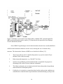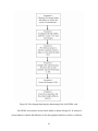
1
MBE GROWTH AND INSTRUMENTATION
Sriteja Tarigopula
Thesis Prepared for the Degree of
MASTER OF SCIENCE
UNIVERSITY OF NORTH TEXAS
May 2006
APPROVED:
Shuping Wang, Major Professor
Terry Golding, Committee Member
Keith Jamison, Committee Member
Vijay Vaidyanathan, Committee Member and
Departmental Coordinator of Electronics
Engineering Technology
Albert B. Grubbs Jr., Committee Member and
Chair of Department of Engineering
Technology
Oscar Garcia, Dean of the College of Engineering
Sandra L. Terrell, Dean of the Robert B. Toulouse
School of Graduate Studies
Tarigopula, Sriteja, MBE Growth and Instrumentation, Master of Science (Engineering
Technology), May 2006, 79 pp., 5 tables, 69 figures, references, 25 titles.
This thesis mainly aims at application of principles of engineering technology in the field
of molecular beam epitaxy (MBE). MBE is a versatile technique for growing epitaxial thin films
of semiconductors and metals by impinging molecular beams of atoms onto a heated substrate
under ultra-high vacuum (UHV) conditions. Here, a LabVIEW® (laboratory virtual instrument
engineering workbench) software* program is developed that would form the basis of a real-time
control system that would transform MBE into a true-production technology. Growth conditions
can be monitored in real-time with the help of reflection high energy electron diffraction
(RHEED) technique. The period of one RHEED oscillation corresponds exactly to the growth of
one monolayer of atoms of the semiconductor material. The PCI-1409 frame grabber card
supplied by National Instruments is used in conjunction with the LabVIEW software to capture
the RHEED images and capture the intensity of RHEED oscillations. The intensity values are
written to a text file and plotted in the form of a graph. A fast Fourier transform of these
oscillations gives the growth rate of the epi-wafer being grown. All the data being captured by
the LabVIEW program can be saved to file forming a growth pedigree for future use. Unattended
automation can be achieved by designing a control system that monitors the growth in real-time
and compares it with the data recorded from the LabVIEW program from the previous growth
and adjusts the growth parameters automatically thereby growing accurate device structures.
*
National Instruments Corporation, http://www.ni.com/legal/termsofuse/unitedstates/us/
H
H
Copyright 2006
by
Sriteja Tarigopula
ii
ACKNOWLEDGEMENTS
I thank my major professor Dr. Shuping Wang for her time, encouragement, attention to
detail, and excellent guidance that have been necessary for this thesis.
I express my gratitude and thanks to my professor, supervisor and committee member Dr.
Terry Golding for his support, confidence, encouragement and guidance throughout my graduate
program and in completing this thesis.
I thank my committee member Dr. Vijay Vaidyanathan for his valuable suggestions,
support and friendly guidance.
I thank the Dr. Albert B. Grubbs, Chair of Engineering Technology Department,
University of North Texas, for his support and encouragement all along my graduate studies.
I express my gratitude to my Industrial representative Mr. Keith Jamison for his time and
support.
I dedicate my thesis to my parents Mr. Sripathi Tarigopula and Mrs. Nagapushpavathy
Tarigopula. I also like to thank my sister Srivamsi Tarigopula and my brother Srinath Chowdary
Tarigopula for their support and encouragement.
I would also like to thank my friends Arun Yelimeli, Dr. Brian Gorman, Ryan Cottier,
Dr.Fatima Amir, Sheetal Liddar, Rekha Vemuri for their help, suggestions and their valuable
time.
iii
TABLE OF CONTENTS
Page
ACKNOWLEDGMENTS ...........................................................................................................iii
LIST OF TABLES........................................................................................................................ v
LIST OF FIGURES ..................................................................................................................... vi
Chapters
I.
INTRODUCTION ................................................................................................ 1
MBE as a Production Technology
Statement of Need
Purpose of Study
Hypothesis
II.
REVIEW OF LITERATURE ............................................................................. 12
Molecular Beam Epitaxy Background
Interference Phenomenon in Light Waves
Electron Diffraction
Reflection High Energy Electron Diffraction
III.
METHODOLOGY/ACQUISITION OF DATA ................................................ 25
Preparing the III/V Chamber of Growth
Experimental Setup for LabVIEW®
IV.
RESULTS AND DISCUSSION ......................................................................... 53
Limitations
V.
CONCLUSIONS................................................................................................. 73
VI.
FUTURE WORK................................................................................................ 76
REFERENCES ........................................................................................................................... 78
iv
LIST OF TABLES
Page
1.
RHEED data from LabVIEW® program........................................................................ 56
2.
Reconstruction of RHEED oscillations in ORIGIN program......................................... 57
3.
Reconstruction of RHEED oscillations in ORIGIN for Dr.Gossmann’s program for
sample-1.......................................................................................................................... 57
4.
Reconstruction of RHEED oscillations in ORIGIN program for LabVIEW® for sample-2
......................................................................................................................................... 62
5.
Reconstruction of RHEED oscillations in ORIGIN for Dr.Gossmann’s program for
sample-2.......................................................................................................................... 62
v
LIST OF FIGURES
Page
1.
Schematic illustration of basic evaporation process for molecular beam epitaxy for
intentionally doped GaAs AlxGa1-x [11] ........................................................................... 3
2.
RHEED Gun setup for MBE growth [11]......................................................................... 4
3.
Block diagram of the control until that can be designed depending on the RHEED
oscillations ........................................................................................................................ 6
4.
Schematic cross section of an advanced three- chamber UHV system designed for MBE
growth and detailed surface studies [16] ........................................................................ 14
5.
Constructive interference and destructive interference in waves [16]............................ 15
6.
Formation of bright and dark streaks of light due to constructive and destructive
interference of light waves [16] ...................................................................................... 16
7.
Crystal translational vectors a,b,c depicting the crystal axis in x,y,z directions [17]..... 18
8.
The above figure shows crystal lattice in a 2-dimensional space. The atomic arrangement
in the crystal looks exactly the same to an observer at r’ and r, provided that the vector T
which connects r’ and r may be expressed as an integral multiple of vectors a and b [17].
......................................................................................................................................... 18
9.
Space lattice [17]............................................................................................................. 19
10.
Basis, containing two different ions [17]........................................................................ 19
11.
Crystal structure [17] ...................................................................................................... 19
12.
Ewald’s sphere for the construction of diffraction pattern in reciprocal lattice space [17]
......................................................................................................................................... 23
13.
Varian 360, III/V MBE growth chamber at UNT........................................................... 26
14.
Group IV MBE system at UNT ...................................................................................... 26
15.
Flow diagram to represent the experimental procedure of the III/V MBE..................... 27
16.
Vacuum pumps on the III/V MBE system...................................................................... 28
17.
Ion pump and cryo-pump on the III/V MBE system ...................................................... 29
18.
Load-lock chamber of the III/V MBE system ................................................................ 31
19.
View port of the load-lock chamber showing the molybdenum blocks and samples..... 32
vi
20.
Preparation chamber of the III/V MBE system .............................................................. 33
21.
Top view of a typical standard MBE system growth chamber [20] ............................... 34
22.
Growth chamber of III/V MBE system .......................................................................... 36
23.
Screen shot of the SpecView program............................................................................ 36
24.
Furnace control unit housing rack................................................................................... 37
25.
RHEED control Equipment housing rack....................................................................... 38
26.
PCI-1409 frame grabber card supplied by National Instruments [23]............................ 39
27.
Experimental setup to capture RHEED images of the III/V MBE chamber using the
LabVIEW® code ............................................................................................................ 40
28.
Flow diagram depicting the functioning of the LabVIEW® code ................................. 41
29.
Front panel showing the various controls for the program ............................................. 44
30.
Front panel showing the Waveform Chart...................................................................... 45
31.
Front panel having the ERROR INDICATORS at various stages of the program ........ 46
32.
Sequence 0, used to select a point on the image at which the measurements will be taken
......................................................................................................................................... 47
33.
Sequence 1, configuring IMAQ buffers for acquisition ................................................. 48
34.
In Sequence 2, a decision is made whether to start the acquisition or to wait further.... 49
35.
Sequence 3, displays an image and measures the intensity on the image....................... 50
36.
Sequence 3 also stops acquisition and writes the data to file ......................................... 51
37.
Sequence 4, writes images to file.................................................................................... 52
38.
Sequence 5, closes the acquisition and releases IMAQ buffers in system memory ....... 52
39.
RHEED oscillations for sample-1 and sample-2 recorded usingLabVIEW® program
......................................................................................................................................... 54
40.
RHEED image before growing Fe for sample-1............................................................. 54
41.
RHEED image for sample-1 during the growth ............................................................. 54
42.
RHEED image for sample-1 after finishing Fe deposition............................................. 55
vii
43.
Reconstruction of RHEED oscillations forLabVIEW® using ORIGIN ........................ 58
44.
Reconstruction of RHEED oscillations for Dr.Gossmann’s program using ORIGIN.... 58
45.
FFT forLabVIEW® for sample-1 ................................................................................... 59
46.
FFT for Dr.Gossmann's program for sample-1............................................................... 59
47.
RHEED reconstruction for sample-2 forLabVIEW® program ...................................... 60
48.
RHEED reconstruction for sample-2 for Dr.Gossmann’s program................................ 61
49.
RHEED image before deposition of Fe on sample-2...................................................... 61
50.
RHEED image during deposition of Fe on sample-2 ..................................................... 63
51.
RHEED image after depositing of Fe on sample-2 ........................................................ 63
52.
FFT for LabVIEW® program for sample-2 ................................................................... 64
53.
FFT for Dr.Gossmann's program for sample-2............................................................... 64
54.
RHEED intensity recording for sample-3....................................................................... 65
55.
RHEED image during initial deposition of Si ................................................................ 66
56.
RHEED image after depositing Si for 8 minutes............................................................ 67
57.
RHEED image when the Fe source is opened ................................................................ 67
58.
RHEED image after depositing Fe for 15 minutes ......................................................... 68
59.
RHEED image after Ge source is opened....................................................................... 68
60.
RHEED image after depositing Ge for 2 minutes .......................................................... 69
61.
RHEED image at the end of depositing Ge .................................................................... 69
62.
Growth pattern reconstructed using ORIGIN software .................................................. 70
63.
FFT of oscillations for Si growth.................................................................................... 71
64.
FFT oscillations for Fe Growth....................................................................................... 71
65.
FFT oscillations for Ge ................................................................................................... 72
66.
MBE system with a feedback control system associated with it. ................................... 76
viii
CHAPTER 1
INTRODUCTION
World’s engineers provide service to a wide range of fields ranging from electronics,
electrical, mechanical, civil, construction to physics, chemistry, transportation, efficient energy
use, new materials, fabrication, new products and manufacturing processes. Engineering
Technology focuses on technological systems and processes with specific industrial applications.
Electronics engineering technology covers hardware and software interfacing, data acquisition
and analysis, computer-aided software engineering, real-time control systems, digital signal
processing and so on. This thesis mainly aims at taking a step towards application of engineering
technology in the field of physics.
Semiconductor structures constitute the building blocks of several electronic and
photonic devices such as such as field effect transistors (FET) [1], hetrojunction bipolar
transistors (HBTs) [2], metal semiconductor field effect transistor (MSFET) [3], high electron
mobility transistors (HEMT) [4], high speed integrated circuits on a single wafer [5], laser diodes
[6], photo detectors [7], light emitting diodes [8], vertical cavity surface emitting laser (VCSEL)
[9]. These devices are used in such applications as fiber-optics, cellular phones, satellites, radar
systems, display devices, microwave devices, radio frequency (RF) devices, Bluetooth wireless
technology, flat panel displays, satellite radio, global positioning system (GPS), wireless local
area network (LAN) [10]. The ever growing demand of high performance semiconductor devices
calls for a need of controlled and precise growth of the semiconductor compounds to achieve the
targeted device properties. Consider for example a VCSEL. In this device the laser is emitted
vertical to the surface of the device. The efficiency of the laser depends of the surface roughness
of the Bragg reflecting mirrors that have very small dimensions (~50nm) and are stacked one
1
over the other. Precise growth of these layers needs very controlled and stringent growth
mechanism.
The choice of semiconductors for synthesizing particular device application is guided by
the specific electrical or optical design requirements, coupled with an ability to grow the required
stack of semiconductor layers epitaxially. Epitaxy is the process of depositing, or growing,
atomically thin crystal layers of typically dissimilar elemental materials onto a substrate to
produce a compound semiconductor. Each crystal layer is known as an epilayer. After the
epilayers are grown on a substrate, it is known as an epiwafer. A novel and the most popular
means to achieve these requirements is to use the molecular beam epitaxy (MBE) growth
process. MBE is a versatile technique for growing epitaxial thin films of semiconductors and
metals by impinging molecular beams of atoms onto a heated substrate under ultra-high vacuum
(UHV) conditions. The basic evaporation process during in the MBE chamber present in UNT is
schematically depicted in Figure 1. The illustration shows the heated substrate. The molecular
beams (flux) reacting on the substrate crystal are generated by thermal evaporation of the
constituent elements or their compounds contained in accurately temperature-controlled effusion
cells. These cells are arranged such that the central portion of their flux distribution intersects the
substrate at an orifice-substrate distance ranging from 60 to 140 mm in various MBE systems
[11]. Each source is provided a shutter that can be controlled mechanically or pneumatically.
Operation of these shutters permits rapid changing of the beam species in order to alter abruptly
the composition and/or doping of growing film normal to the surface with a slow growth rate of
up to 0.1-2.0μm/hr. As a consequence, abrupt material interfaces can be achieved, since any
significant bulk diffusion is eliminated at the specific low growth temperature of MBE. In
2
addition, mechanical masks may be inserted into the paths of the beam fluxes to create any
desired device geometry.
Figure 1. Schematic illustration of basic evaporation process for molecular beam epitaxy for
III/IV MBE chamber present in University of North Texas (UNT).
MBE allows growth of crystalline layer combinations with accurate dimensional control
down to the atomic level. This precision would not be possible without adequate accurate
characterization techniques. One of the most useful tools for in situ monitoring of the crystal
growth is the reflection high-energy electron diffraction (RHEED) system. RHEED provides
resolution on the atomic scale while at the same time being fully compatible with the crystal
growth process. The layout of a typical RHEED system is shown in Figure 2. A typical RHEED
measurement system consists of an electron gun, a phosphor screen and image processing
hardware and software. The RHEED gun emits ~10KeV electrons which impinge the
semiconductor surface at a shallow angle (~0.5-2o) [11]. The incident electrons diffract from the
3
surface of the sample wafer and strike a phosphor screen forming a pattern of dark and bright
lines, which is indicative of the surface crystal structure. A camera monitors the screen and can
record instantaneous pictures or measure the intensity of the image at a given pixel as a function
of time. The intensity of the RHEED image keeps changing from time to time or in other words
the intensity keeps oscillating. It has been well established that the period of these oscillations
corresponds exactly to the growth of one monolayer of atoms of the semiconductor material
during the growth [12]. RHEED is therefore used to calibrate growth rates, observe removal of
oxides from the surface, calibrate the substrate temperature and monitor the arrangement of the
surface atoms and to give a feedback on surface morphology during growth.
INCIDENT
BEAM
DIFFRACTED
BEAM
CAMERA
RHEED GUN
SUBSTRATE
RHEED SCREEN
Figure 2. RHEED Gun setup for MBE growth. Adapted from [11].
MBE as a Production Technology
MBE has gone through a lot of development and refinement over the past two decades
and has transformed itself to near production-ready technology. Commercial MBE vendors have
made a great amount of progress in terms of producing clean wafers and source cells with
accurate dimensions. For advanced epi-based structures such as HEMTs and HBTs, MBE is
capable of preparing these extremely complex structures with atomic layer precision. However,
important concerns in mass production of these materials are reproducibility from run to run,
over period of times and from systems to systems. Frequent system calibration runs and test runs
4
still have to be prepared routinely. These non-productive runs increase average cost and reduce
growth yield. Moreover, processing specifications of many devices are tightened because
Stricter tolerance of certain critical parameters can significantly impact the cost of producing
high-performance, low cost modules and circuits. This calls for automating the MBE growth
process to improve wafer to wafer processing repeatability, reduce run-time by eliminating error
prone process to produce devices on a large scale without compromising on the quality of the
device structures grown.
Unattended automation can be achieved by designing a control system that monitors the
growth in real-time and compares it with the data available from the previous growth. The
difference between the real-time data and ideal data can be calculated and feedback to the control
system and the growth parameters can be adjusted in real-time, thereby achieving accurate
device structures. The variables that strongly effect the layer growth are the substrate
temperature and flux emitting from the individual source materials. In the MBE reactor, it is not
possible to rapidly change the diffusion (by controlling surface temperature) over the time period
of typical 5-10 monolayer growth because of the slow thermal dynamics of the substrate. Hence,
substrate temperature is useful as a "run-to-run" control variable. Flux on the other hand can be
rapidly changed by adjusting the effusion cell shutters, and more slowly changed by controlling
the cell temperature. Hence, flux is the effective control variable. A change in flux will effect the
deposition time to achieve a desired coverage, i.e., decreasing flux increases the deposition time
to reach a coverage goal and vice versa.
Growth conditions can be monitored in real-time with the help of RHEED data, since the
period of one RHEED oscillation corresponds exactly to the growth of one monolayer of atoms
of the semiconductor material [12]. These RHEED oscillation patterns can be observed from
5
time to time and compared to previously available data of the same material being grown. If it is
observed that a known growth pattern is not being followed then the growth conditions such as
the temperature of the source cells and also control the movement of the shutters in front of the
source cells can be altered. A schematic depiction of such a system is shown in Figure 3 . The
wafers are grown in the MBE chamber, and the RHEED images are observed on the computer
and the real-time data is compared against the already available data. If any changes are to be
made in the growth conditions, the computer calculates these values and sends the signals to
change the temperature of the source cells or the control the movement of the shutters in front of
the source cells. In addition to this, the current data being captured can also be saved for future
reference.
TEMPERATURE
CONTROL UNIT
COMPUTER
WITH RHEED
DATA
SHUTTER
CONTROL UNIT
III/V MBE system
Figure 3. Block diagram of the control until that can be designed depending on the RHEED
oscillations.
6
Statement of Need
RHEED oscillations can be monitored either manually or by using a software program.
The software that was present in the III/VMBE lab to record the RHEED data is called the Video
RHEED Intensity Measurement Program (RHEED program) [13]. With this system, the intensity
of diffracted beams can be measured simultaneously. The RHEED program used a Panasonic™
CCD camera * (Model No: WV-BD400) to monitor the images continuously and take the
intensity measurements using a video card. The intensity of the diffracted beams is also
displayed in real time on the video monitor, enabling the user to monitor the growth in real time.
After data acquisition is finished, the RHEED intensity oscillations are either scanned with a
movable cursor to determine the period of the oscillations or analyzed using a fast Fourier
transform (FFT) to give a growth rate.
The video intensity measurement board is not a “frame grabber”. Instead, it breaks up the
video screen into a matrix of 256*256 pixels with 256 gray levels per pixel. The intensity from a
given pixel is read by sending the address of that pixel to the video digitizing board, waiting until
the chosen pixel is digitized, and then reading the digitized intensity. The video digitizing board
displays a bright point at the selected pixel location on the video monitor while the selected pixel
is digitized.
At normal video camera line frequency (~15 KHz), the video digitizing board can digitize
one data point with each horizontal line scan of the video camera. Therefore, the maximum data
acquisition rate is one vertical line (having a maximum of 256 points) every 1/60th of a second.
Because a normal video signal is composed of 2 interlaced 256 line scans, it is possible to record
a vertical line of 512 points every 1/30th of a second. Data acquisition speed of the video
digitizing board is optimized by using vertical data windows one pixel wide that do not overlap
*
Matsushita Electric Industrial Co., Ltd., http://www.panasonic.com/pol_docs/copyright-prv.html
H
7
horizontally. Increasing the data window width reduces the data acquisition speed by the inverse
of the window width. (Data acquisition speed = window width/60 seconds per point for non
overlapping windows).
However, this program crashed and could not be restored. The company that supplied this
software is closed, so a replacement could not be obtained. When the software was functional,
the program did not have an option to record the images before, during and after the growth of
the semiconductor material. It is important to save the RHEED images so that they can be used
in future growths when similar materials are being grown. For example, if a sample material is
grown in ideal conditions and gives accurate results, the RHEED images obtained during this
growth cycle can be used to compare with the RHEED images that are obtained during mass
production. If it is seen during a sample growth (during mass production) that the RHEED
images differ from the ideal images already available then, necessary corrections can be made to
the growth conditions.
Also, the data was recorded only in the form of a graph, it could not be written to a file
like an EXCEL sheet so that it could be analyzed further for more accurate results. For example,
if the data was being recorded every 0.03 seconds, and large number of oscillations are observed
between 1.35 to 1.39 seconds. Then there is no way of zooming in and out of these oscillations in
a given time range for in-depth study of these oscillations. And since the data cannot be written
to an external file, it cannot be reproduced again for further analysis.
Also, if the recording of oscillations was stopped at a particular point of time, (like to
alter the temperature of the sample being grown or the temperature of the source cell) new
oscillations could not be appended to the existing file which makes it difficult to observe the
8
change in oscillations accurately when the temperature is varied. Each time a new file had to be
opened to record the oscillations.
Also, the RHEED program used two different monitors to run the program, one to view
the images (a video monitor) and one to display the oscillations (computer). The user did not
have a choice to change or specify the rate at which the oscillations are recorded like every 0.05
seconds or 0.07 seconds. Also the RHEED program and the video card did not have the
necessary software and hardware interface associated with it so that it can form the basis of a
real-time control unit as shown in Figure 3.
8H
Purpose of Study
The main purpose of the study is to develop a software program which would form the
basis of in situ monitoring of MBE growth for the development of a production ready MBE.
TheLabVIEW® (laboratory virtual instrument engineering workbench) software * has the
1F
necessary software to overcome the limitations in the Video RHEED Intensity Measurement
Program. The PCI-1409 frame grabber card also supplied by National Instruments is used in
association with the LabVIEW® software to capture the RHEED images and calculate the
intensity of the oscillations. The LabVIEW® program developed in the lab performs the
following functions:
*
1.
Measure the intensity at a particular point on the image through a Panasonic CCD
camera and using a frame grabber card (PCI-1409) to read the intensity values.
Plot the intensity values as Time vs. Amplitude graph.
2.
Observe the RHEED images continuously on the same computer monitor that has
the LabVIEW® code in it. The record the RHEED images before, during and at
the end of the sample growth. Able to change the point of measurement on the
image during the growth.
National Instruments Corporation, http://www.ni.com/legal/termsofuse/unitedstates/us/
H
H
9
3.
Write the recorded intensity and the time values to an EXCEL spreadsheet. While
growing different samples the user should have a choice to append the data to an
existing file or write data to a new file. The program has flexibility to record the
intensity values at different time intervals such as 20ms, 50 ms or 30ms and so on
as specified by the user.
4.
User friendly interface, the end-user need not have a working knowledge of
LabVIEW® to operate the program.
5.
This program is portable. That is it does not depend on the MBE system that is
being used to take the measurements. It can be used in conjunction with any MBE
system that has RHEED in it.
Once the data is obtained the fast Fourier transformation (FFT) calculations will be made on
the data to calculate the crystal growth rate. The research will also include operating the
electronics associated with the III/V MBE system to get a real world experience of the semiconductor industrial technology. Since there is a need to validate the results obtained using the
new LabVIEW® code, these results are compared to an existing RHEED program present on the
group IV MBE system in the lab. The GROUP IV MBE uses a program developed by Dr. Hans
Gossmann to record the RHEED oscillations. This program is similar to the Video RHEED
Intensity Measurement Program with a single exception that the data can be written to a text file
(.txt) file. The LabVIEW® program has been able to achieve similar results as in Dr.Gossmann’s
program. The program is now working and it can be further expanded to have a real-time control
system shown in Figure 3.
9H
Hypotheses
Null Hypothesis: A working LabVIEW® code cannot be written as an alternative to the
Video RHEED Intensity Measurement Program, to monitor the growth of semiconductor
materials grown using the III/V MBE system.
10
Alternate Hypothesis: A working LabVIEW® program can be created as an alternative to
the Video RHEED Intensity Measurement Program, to monitor the growth of semiconductor
materials grown using the III/V MBE system.
11
CHAPTER II
REVIEW OF LITERATURE
Molecular Beam Epitaxy Background
The original ideas for molecular beam epitaxy (MBE) of III-V compound semiconductors
was first proposed by Gunther in 1958 [14], it was not until 10 years later that epitaxy of monocyrstalline GaAs layers was achieved [15] using high improved vacuum conditions. MBE is a
form of evaporation. It distinguishes itself from other evaporative crystal growth methods by
employing a design that allows high quality epitaxial layers, with excellent carrier transport and
optical properties to be prepared. The pursuit of higher vacuum conditions, by incorporation of a
liquid-nitrogen-cooled shroud surrounding the evaporation sources and the use of ultra high
vacuum pumps, achieved a pressure of about 10-9 torr in the early 1970s. It was the in-situ
evaluation of crystal growth condition by reflection high-energy electron diffraction (RHEED)
that led to the understanding of substrate cleaning, a proper epitaxial growth temperature and
deposition rate.
The guidelines for achieving stoichiometric compounds by MBE have been found [15] in
the surface chemical dependence of the sticking coefficient, S, of various species. S is defined as
the fraction of total impinging atoms or molecules that sticks to the surface and is incorporated in
the film. Generally, for III/V compounds only that amount of the group V element adheres to the
growing surface, which collides with excess group III atoms on the surface and reacts to form the
III-V crystal. As a result, one group V atom sticks for each group III atom, and epitaxial growth
on the III-V substrate occurs [16].
During the growth process temperatures of the individual effusion cells control the
intensities of beams incident on the heated substrate crystal. For typical growth rates of ~1µm/hr,
12
the fluxes required on the growing surfaces are approximately, 1014-10 15 atoms/ cm2s for group
III elements, 1015-10 16 atoms/ cm2s for group V elements and 107-10 12 atoms/cm2 s for dopants
[15]. Continuous changes in the chemical composition of the growing film are achieved by
programmed variation of the cell temperatures. As mentioned earlier, abrupt changes are
obtained by using mechanical shutters interposed between the cell orifice and substrate. The
group III element beam is always atomic, while the beam of the group V element can be either
diatomic when generated by incongruent evaporation of the III-V compound itself or tetratomic
when generated from elemental source.
The slow growth rate during MBE coupled with obvious stringent demand for low
unintentional impurity levels incorporated in the deposited material require a clean UHV
environment in the growth chamber. Thus, the equipment for MBE is basically a stainless steel
UHV system with a background pressure below 10-10 Torr pumped by standard ion pumps or by
suitably trapped diffusion or turbomolecular pumps, respectively. Additional liquid nitrogen
(LN2) cryopanels assure that the partial pressures of gases with high sticking coefficient. (E.g.
OH-containing species), are kept even below 10-14 Torr in the vicinity of the growing crystal
[15]. In practice, during deposition, the total pressure in the reaction chamber rises above 10-9
Torr because of the scattered beam species. However, the UHV condition is always maintained
with respect to impurity species.
A complete multichamber system designed for growing and extensively characterizing
surfaces and multilayer epitaxial films is schematically depicted in Figure 4. The system utilizes
10H
three separate vacuum chambers connected via large diameter channels and isolation valves in a
linear or angular configuration. The integral self-contained system essential for the crystal
growth consists of the growth chamber and the load lock chamber/sample introduction chamber.
13
Figure 4. Schematic cross section of an advanced three- chamber UHV system designed for
MBE growth and detailed surface studies. [15]. Reproduced with permission from Springer
Science and Business Media.
1H
One of MBE’s big advantages is the fact that hazardous chemicals are usually handled in
solid form and contained within the vacuum vessel, reducing the cost of external safety
measures. The characteristic features of MBE are as described as follows [15]:
1.
The slow growth rate of 0.1-2.0μm/hr that permits very precise control of layer
thickness in the submicron range.
2.
Reduced growth temperature, e.g., 500-600oC for GaAs.
3.
Specific non-equilibrium growth mechanism that is responsible for progressive
smoothing of the surface for most substrate orientations.
4.
The ability to abruptly cease or initiate molecular beams that produces hyperabrupt
material interfaces and dopant profiles
5.
Facility for in situ analysis to assure that desired surface and reaction conditions are
reached before commencement of growth and are maintained during crystal growth.
14
Therefore, the study of MBE plays an important role in the development of high
performance semiconductors used for several electronic and photonic devices.
Interference Phenomenon in Light Waves
Interference is the superposition (overlapping) of two or more waves (having same
frequency) resulting in a new wave pattern [16]. Consider two waves shown in Figure 5. When
12H
two waves superimpose, the resulting waveform depends on the frequency, (or wavelength)
amplitude and relative phase of the two waves. If the two waves have the same amplitude A and
wavelength the resultant waveform will have amplitude between 0 and 2A depending on whether
the two waves are in phase or out of phase.
combined
waveform
wave 1
wave 2
0H
Two waves in phase
Two waves 180° out of phase
.
Figure 5. Constructive interference and destructive interference in waves. Adapted from [16].
Consider two waves that are in phase, with amplitudes A1 and A2. Their troughs and
peaks line up and the resultant wave will have amplitude A = A1 + A2. This is known as
constructive interference. If the two wave's are 180° out of phase, then one wave’s hump will
coincide with another wave's trough and so will tend to cancel out, resulting in destructive
interference. The resultant amplitude is A = |A1 − A2|. If A1 = A2 the resultant amplitude will be
15
zero. Thomas Young demonstrated this phenomenon in light waves through his popular
experiment known as the Young’s experiment. Consider two coherent light sources spaced
closely at two narrow slits, shown in
13H
Figure 6. In such an arrangement, the light waves emerging from the slits are in phase
and this leads to a pattern of bright and dark bands on the screen called as interference fringes
when a screen is placed in the path of these waves. Whenever constructive interference occurs
between the two light sources a bright fringe is observed on the screen, shown in
14H
Figure 6. When destructive interference occurs between the two light sources a dark
fringe is observed on the screen. This leads to a pattern of bright and dark fringes on the screen.
This experiment can also be performed on a beam of electrons and atoms showing similar
interference patterns.
Figure 6. Formation of bright and dark streaks of light due to constructive and destructive
interference of light waves. Adapted from [16].
16
Electron Diffraction
An ideal semiconductor crystal is composed of atoms arranged on a lattice defined by
three fundamental translational vectors a,b,c such that the atomic arrangement looks the same in
every respect when viewed from any point r as when viewed from the point r’ [17] shown in
Figure 7 and Figure 8,
15H
16H
r
r r
r
r
r ' = r + ua + vb + wc
(1)
where, u, v, w are arbitrary integers.
r
The set of points r ' specified by (1) for all values of integers u, v, w define a lattice. A
lattice is a regular periodic arrangement of points in space. The crystal structure is formed only
when a basis of atoms is attached identically to each lattice point. The logical relation is,
lattice + basis = crystal structure
(2)
The lattice and the translation vectors a,b,c are said to be primitive if any two points, r,
r’ from which the atomic arrangement looks the same, always satisfy (1) with a suitable choice
of integers u, v, w . This definition of the primitive translation vectors guarantees that there is no
cell of smaller volume that could serve as a building block for the structure. The crystal axes
a,b,c form three adjacent edges of a parallelpiped. If there are lattice points only at the corners of
the parallelpiped, then it is defined as a primitive parallelpiped. A lattice translation operation is
defined as the displacement of a crystal parallel to itself by a crystal translation vector,
r
r
r
r
T = ua + vb + wc
Any two lattice points are connected by a vector of this form and are shown in Fig 4.
17
(3)
Figure 7. Crystal translational vectors a,b,c depicting the crystal axis in x,y,z directions. Adapted
from [17].
Figure 8. The above figure shows crystal lattice in a 2-dimensional space. The atomic
arrangement in the crystal looks exactly the same to an observer at r’ and r, provided that the
vector T which connects r’ and r may be expressed as an integral multiple of vectors a and b.
Adapted from [17].
Attached to every lattice point there is a basis of atoms, with every basis identical in
composition, arrangement and orientation. A crystal structure is formed by the addition of a basis
to every lattice point. The lattice points are shown in Figure 9. The basis is indicated by dots in
17H
Figure 10. In Figure 11 the dots are omitted and each lattice point is replaced by the crystal basis.
18H
19H
18
The number of atoms in the basis may be as low as one, as for many metals and inert gases, but
there are some structures for which the basis exceeds 1000 atoms. The position of the center of
the atom j of the basis is given by,
r
r
r
r
rj = x j a + y j b + z j c
relative to the lattice point.
Figure 9. Space lattice. Adapted from [17].
Figure 10. Basis, containing two different ions. Adapted from [17].
Figure 11. Crystal structure. Adapted from [17].
19
(4)
Equation (3) shows that a crystal is invariant under any translation of the form
r
r
r
r
T = ua + vb + wc , where u, b, w integers and a, b and c are the crystal axes [17]. Any physical
property of a crystal is invariant under T. The charge concentration, the electron number density,
the mass density and the magnetic moment density are invariant under all translations T. Thus
r
r
the electron number density n(r ) is a periodic function of r with a period a,b,c in the directions
r r
r
of the three crystals axes, whence n(r + T ) = n(r ) .
Most properties of a crystal can be related to the Fourier components of the electron
density [17]. Consider a function n(x) with a period ‘a’ in one dimension. Expanding n(x) in a
Fourier series of cosines and sines:
n( x) =n 0 + ∑ ⎡⎢C p cos⎛⎜ 2πpx ⎞⎟ + S p sin ⎛⎜ 2πpx ⎞⎟⎤⎥
a⎠
a ⎠⎦
⎝
⎝
p >0 ⎣
(6)
Where, the p’s are positive integers and C p and S p are real constants, called the Fourier
coefficients of the expansion. The factor 2π / a in the arguments ensures that n(x) has a period a:
n( x + a ) = n 0 + ∑ ⎡⎢C p cos⎛⎜ 2πpx + 2πp ⎞⎟ + S p sin ⎛⎜ 2πpx + 2πp ⎞⎟⎤⎥
a
a
⎠⎦
⎝
⎠
⎝
p >0 ⎣
= n 0 + ∑ ⎡⎢C p cos⎛⎜ 2πpx ⎞⎟ + S p sin ⎛⎜ 2πpx ⎞⎟⎤⎥
a ⎠⎦
a⎠
⎝
⎝
p >0 ⎣
= n(x)
(7)
Here, 2π / a is a point in Fourier space or in other words a point in the reciprocal lattice of the
crystal. In one dimension these points lie on a line. The reciprocal lattice points tell us the
20
allowed terms in the Fourier series (6). A term is allowed if it is consistent with the periodicity of
the crystal, as in Figure 9, other points in the reciprocal space are not allowed in the Fourier
20H
expansion of a periodic function.
Equation (6) can be rewritten as [17],
n( x ) = ∑ n p e
i 2πp
a
(8)
p
where the sum is over all integers p:positive, negative and zero. Extending the analysis to three
dimensional lattice structures, equation (8) can be written as,
r r
n( x) = ∑ nGr e iG⋅r
(9)
p
r
where G is called the reciprocal lattice vector and is given by,
r
r
r r
G = hA + kB + lC
r r
r
b
A = 2π × c r r r ;
a ⋅b ×c
r r
r
B = 2π c × a r r r ;
a ⋅b ×c
r r
v
a
C = 2π × b r r r
a ⋅b ×c
(10)
(11)
Where, h, k, l are integers. Any arbitrary set of primitive vectors a, b, c of a given crystal lattice
r
leads to the same set of reciprocal lattice points given by equation (10). Any vector G of this
form is called a reciprocal lattice vector.
Every crystal structure has two lattices associated with it, the crystal lattice and the
reciprocal lattice. A diffraction pattern of a crystal is a map of the reciprocal lattice, of the
crystal, in contrast to a microscope image, which is a map of the real crystal structure. The two
21
lattices are related by the definitions (11). When the crystal is rotated, both the direct lattice and
the reciprocal lattice are rotated. Vectors in the lattice have dimensions of [length]; vectors in the
reciprocal lattice have the dimensions of [length]-1. The crystal lattice is a lattice in real or
ordinary space; the reciprocal lattice is a lattice in the associated Fourier space. A helpful tool for
drawing the diffracted pattern is the Ewald's construction shown in Figure 12.
21H
The spots on the right hand side and the reciprocal lattice rods represent the diffraction pattern in
the reciprocal lattice space. The vector K is drawn in the direction of the incident electron beam
and it terminates at any reciprocal point. A sphere is drawn with a radius equal to k=2π/λ about
the origin of K. The diffracted beam will be formed if this sphere intersects any other point in the
reciprocal lattice. The sphere as drawn intercepts a point connected with the end of K by a
reciprocal lattice vector G. The diffracted beam is in the direction Ki=K+∆k where ∆k= G. The
construction was demonstrated by P.P.Ewald [17]. This is because after the completion of the
growth the sample is smooth and uniform causing 2-dimensional diffraction to occur. The
diffraction spots in the reciprocal lattice space are therefore close to each other and appear in the
form of rods or streaks on the screen.
The RHEED patterns are therefore a symbolic representation of the surface morphology
of a crystal. These patterns need to be recorded to observe and record the crystal growth pattern.
These pictures can then be used for future studies to grow required semiconductor materials.
First a single sample can be grown and the RHEED images can be recorded. When it is required
to start mass production of the same semiconductor material these RHEED images can be used
to compare and predict the growth of the crystals being grown. If the samples under mass
production have RHEED images different from the earlier recorded ones, these can be discarded
22
Reciprocal lattice points
RHEED spots
Diffracted beam, ki
Ewald’s sphere
Incident beam, k
Sample surface
Figure 12. Ewald’s sphere for the construction of diffraction pattern in reciprocal lattice space.
Adapted from [17].
or the growth conditions be altered to achieve the required growth. By discarding the bad
materials the cost and time involving in mass production of semiconductor materials is reduced
significantly. New semiconductor materials can be grown in the place of defective samples
thereby increasing the final quality and throughput of the mass produced semiconductor devices
resulting in increased revenues and consumer satisfaction.
Reflection High Energy Electron Diffraction
The intensity of the RHEED oscillations also varies during the growth. When a layer
23
starts it has a smooth surface and the incident electrons undergo minimum diffraction when they
are incident on the surface of a sample. Consequently the RHEED pattern is bright and has
maximum intensity. As the layer nucleates, islands form on the surface, and the electrons
undergo maximum diffraction leading to decrease in the RHEED pattern intensity. As the layer
finishes, the islands coalesce into a flat layer, and the intensity of the RHEED pattern increases.
Therefore, the period of one oscillation corresponds exactly to the growth of one monolayer of
the semiconductor material during the growth [12]. RHEED is therefore used to calibrate growth
rates, observe removal of oxides from the surface, calibrate the substrate temperature and
monitor the arrangement of the surface atoms and to give a feedback on surface morphology
during growth.
24
CHAPTER III
METHODOLOGY/ACQUISITION OF DATA
This chapter consists of two main sections: (a) Preparing the III/V chamber for growth
and (b) Experimental setup for image capture and analysis.
The first section discusses in detail as to how the III/V molecular beam epitaxy (MBE)
system is setup for growing wafers and the second section describes how the PCI-1409 frame
grabber card is interfaced to the computer using the LabVIEW® software * to capture the
2F
reflection high-energy electron diffraction (RHEED) images of the sample being grown.
Preparing the III/V Chamber for Growth
The III/V and group IV MBE chambers present in the physics lab at UNT are shown in
Figure 13 and Figure 14, respectively. Before the beginning of this thesis, the III/V chamber [18]
2H
23H
24H
had not been used for any type of growth for the past 5 years. This had led to the accumulation of
residues such as carbon, arsenic, oxygen, nitrogen, gallium and water from the previous growths.
The sample holders had also been left in the chamber for a long time, resulting in the deposition
of unwanted residues on the surface of the sample holders. The view ports of the III/V chamber
are also unclear, blocking the view of the load-lock, preparation and growth chambers for
observation during the growth. The view ports, sample holders have to be cleaned using proper
procedures before starting the growth. Secondly the crucibles which hold the individual
materials such as Ga, As, P etc., that are used for depositing have also to be checked for residue
material and it is to be determined if empty crucibles have to be filled with required materials. A
step-by-step representation of the experimental procedure to set-up the III/V MBE system for
*
National Instruments Corporation, http://www.ni.com/legal/termsofuse/unitedstates/us/
H
H
25
Figure 13. Varian 360, III/V MBE growth chamber at UNT.
Degass chamber and
Growth chamber
Load-lock chamber
Figure 14. Group IV MBE system at UNT.
26
growth is shown in Figure 15. The MBE chamber is usually under very low pressures of the
25H
range of 10-8 to 10-10 Torr. The chamber should be bought to atmospheric pressure before
performing any maintenance procedures. The different vacuum pumps operating on the system,
shown in Figure 16 and Figure 17 are: mechanical pump (2); turbo pump (1); ion pump (3); and
26H
27H
cryo-pump (1).
Figure 15. Flow diagram to represent the experimental procedure of the III/V MBE.
27
Figure 16. Vacuum pumps on the III/V MBE system.
The vacuum pumps are shut down one after another. Materials such as arsenic are poisonous,
hence lab coats, face masks, head masks, hand gloves, protective eye glasses have to be worn
before opening the system to avoid contact with any hazardous materials. The view-ports are
cleaned first. A solution of H2SO4: H2O2: De-ionized water in the ratio of 1:2:10 is prepared
before hand to clean the view ports as soon as they are removed from the MBE system. The
view-ports are removed from the system from the MBE system so that the other side of the viewport can also be cleaned and the opening created on the MBE system because of this is covered
with aluminum foil to prevent any dust particles or impurities entering the system. After
detaching from the main system the view ports and cleaned repeatedly using the above prepared
solution. It is not advisable to immerse the view ports in this solution because usage of this
28
solution in large amounts will etch away the glass on the view ports. Finally the view ports are
rinsed with de-ionized water.
Growth Chamber
Cryo-pump
Ion-pump – 3
(Inside the enclosure)
Figure 17. Ion pump and cryo-pump on the III/V MBE system.
After opening the view ports the substrate holders are removed from the system. The
substrate holders used in this system are made of molybdenum. A solution of HCl:H2NO3:Deionized water in the ratio of 1:2:1 is prepared and the molybdenum blocks are cleaned repeatedly
using a wipe cloth. Finally the molybdenum blocks are rinsed in de-ionized water.
The screws of the crucible holders are undone and the crucibles are removed from their
holders. The crucibles are made of high purity pyrolytic boron nitrate, extreme fine handling is
required while undoing the screws and removing the crucibles from their holders. The crucibles
are checked for any damage. If they are cracked or completed destroyed they are replaced by
new ones. Good crucibles are checked if sufficient amount of semiconductor material is present
in the crucibles, if not new material is ordered.
29
The linear transfer rod on the system is used to transfer the substrates from the loading
chamber to the growth chamber. This rod has to be aligned in a straight line so that the substrates
don’t hit against the system walls during the transfer. There are four screws on the transfer rod
for this purpose. The two screws on the top and bottom on the rod are used for vertical
alignment. Two more screws on the right and left sides of the transfer rod are used for horizontal
alignment. These screws are adjusted accordingly to correct any misalignment.
The samples used during the growth come in epi-ready form. The GaAs wafers were
received in an epiready state, i.e., the surface was smooth enough to warrant an epitaxial growth,
however, to ensure the optimal surface conditions the wafers are first cleaned in
trichloroethylene, rinsed in methanol, and etched in 5:1:1 mix of H2O:H2O2:H2SO4 for 3 minutes,
then rinsed in running deionized (DI) water for 2 minutes and then blow dried with nitrogen.
Cleaning of the sample results in the formation of a protective oxide layer on the sample. The
samples are then mounted on the molybdenum block (or in short, moly-block) using indium. The
loading chamber has a capability of holding 8 substrates at a time so, 8 moly-blocks are mounted
with samples at a time and are kept ready for growth.
Preparing Samples for Growth
The cleaned view ports and any new components ordered for the system are put back on
the system at this time. The isolation valves between the load-lock and preparation chamber,
preparation and growth chambers are closed. The turbo pump and mechanical pumps are
connected to the load-lock chamber. The turbo pump is used to pump down the load-lock
chamber. When the pressure reaches approximately 10-1 Torr the turbo pump is shut down and
the mechanical pumps are started at the same instant. When the pressure reaches approximately
30
10-4 Torr the isolation valves are opened and the entire system is allowed to pump down using
the mechanical pumps for approximately 12 hours. Then the ion pumps and the cryo-pumps are
turned on and the mechanical pumps are shut down. The system is pumped down using the ion
pumps to the least achievable atmospheric pressure usually 10-10 to 10-12 Torr. The system is left
to pump down for about 48 hours to create the UHV conditions.
After the required pressure is achieved, the load-lock chamber is isolated from the rest of
the chamber and using the isolation valve present between the load-lock chamber and the
preparation chamber, shown in Figure 18. It is then bought to atmospheric pressure. The moly28H
blocks are then mounted manually on the carousel holder, shown in Figure 19.
29H
Figure 18. Load-lock chamber of the III/V MBE system.
31
Figure 19. View port of the load-lock chamber showing the molybdenum blocks and samples.
The view-port is closed again tightly and is pumped down using the mechanical and turbo
pumps. This is done overnight. After this, the isolation valve between the load-lock and
preparation chamber is opened and the system is again allowed to pump down to remove any
pressure difference between the load-lock chamber and the main chamber. After this, the molyblocks are transferred from the load-lock to the preparation chamber using the linear-transfer rod,
one at a time. Now, the isolation valves between load-lock and preparation chamber, preparation
and growth chambers are closed.
The sample is then heated in the preparation chamber. This heating process removes the
protective oxide layer that was formed on the sample after the cleaning process. This process is
also known as de-oxidation and is done by heating the sample to a previously calibrated
temperature (e.g. ~600oC for GaAs) for a few minutes. In addition to these the samples may also
contain carbon and hydrogen atoms as impurities. These can be removed by heating the sample
to a previously calibrated temperature (e.g. 200oC for GaAs) in the preparation chamber and the
process is known as degassing. Performing the degassing and deoxidation functions in the
32
preparation chamber prior to the sample growth in the growth chamber, primarily reduces the
presence of impurities in the growth chamber. The preparation chamber is isolated from the
growth chamber through another isolation valve as shown in Figure 20.
30H
Figure 20. Preparation chamber of the III/V MBE system.
The growth chamber is where the final growth of the sample takes place. The schematic
diagram of the growth chamber is as shown in Figure 21 [15]. This chamber houses the RHEED
31H
32H
electron gun, fluorescent screen to observe the RHEED images, liquid nitrogen (LN2) cryopanels to circulate liquid nitrogen during growth, effusion cells with shutters, furnaces to heat the
effusion cells, ion gauges to measure the chamber pressure, isolation valve between the growth
chamber and preparation chamber, a manipulator, view port to observed the sample during
growth. The thermal stability of the effusion cells is ensured by isolating them through LN2
33
cooling. For this purpose the chamber has two built in cryoshrouds, one in the flange containing
the cells and the other in the growth chamber. The cooling also served the purpose of reducing
the pressure in the chamber, and thus, the amount of contaminants during the growth. The
furnaces and the thermocouples, attached to the back of the crucibles are in closed loop
configuration with temperature controllers, which kept the temperature. Separate controls exist
for the RHEED gun and the manipulator outside the chamber. The samples are placed and
withdrawn from the chamber using the linear transfer rod. The manipulator was mounted along a
horizontal axis and it provided facility to automatically continuously rotate and heat the
substrate. The substrate can be positioned, with respect to the beam sources, at any angle
between horizontal and vertical. It also includes, X, Y, Z motions, thus allowing the RHEED
beam incidence angle to be varied. The manipulator has a non-inductively wound high efficiency
Tantalum(Ta) radiation foil, which allows substrate heating to temperatures up to 800οC.
Figure 21. Top view of a typical standard MBE system growth chamber [15]. Reproduced with
permission from Springer Science and Business Media.
3H
34
The Varian MBE 360 growth chamber is as shown in Figure 22. There are 7 effusion
34H
cells in this chamber, one each for Bi, Al, As, In, P, Sb and Ga. The RHEED gun is operated
typically at 9.5KeV. After the sample is deoxidized and degassed in the preparation chamber, the
isolation valves are opened and the sample is transferred to the growth chamber using the linear
transfer rod. The growth chamber has a manipulator, which has an arrangement to hold the molyblock. After the transfer is complete the linear transfer rod is removed from the growth and
preparation chambers and is pulled out all the way back to the load-lock chamber. The isolation
valve between the growth chamber and the preparation chamber is then closed. The individual
effusion cells are heated using furnaces for depositing the materials on the sample. For practical
growth, the recommended substrate temperature for MBE for GaAs ranges from 500 to 630οC
[20]. The shutters can be opened and closed manually by using the Shutter Control switches
35H
shown in Figure 22. Liquid nitrogen is circulated around the growth chamber during the growth,
36H
to isolate the temperatures of the individual effusion cells from each other and to maintain
appropriate growth temperature in the chamber. During deposition the diffracted electrons from
the surface of the sample can be observed on the phosphor screen, shown in Figure 22.
37H
35
Figure 22. Growth chamber of III/V MBE system.
Figure 23. Screen shot of the SpecView program.
The SpecView software that came with the MBE equipment, was already installed and
working before getting started on the LabVIEW® program. Using this software, the current
36
temperature of the source cells and the substrate can be observed and changed. Figure 23 shows
38H
8 rectangular blocks for each control. Each rectangular block shows two different values of
temperatures. The top value is specified by the user i.e., the required temperature that is required
and can be entered using the keyboard, the bottom value is the current temperature being read by
the controller and changes continuously. When the user enters the required value, the SpecView
Software sends signals to the PID (Proportional Integral Derivative) controllers [21], which
39H
apply current to the furnaces to control the furnace temperatures of the effusion cells and the
substrate The temperature of the effusion cells can also be controlled manually, the control rack
which houses the controls panels and equipment for this purpose is shown in Figure 24. Each
40H
control panel has individual push buttons to increase or decrease the temperature manually.
Figure 24. Furnace control unit housing rack.
37
RHEED control Equipment housing rack is housed in a separate rack as shown in Figure
41H
25. The voltage and the current to the electron gun can be controlled using this control unit. This
unit also consists of control units for ionization gauge and the manipulator control.
Figure 25. RHEED control Equipment housing rack.
Experimental Setup for LabVIEW®
Until now the process of setting up the MBE system to grow wafers has been discussed.
Now, the experimental setup to capture the RHEED images shall be described.
This will include a description of the hardware used to capture the RHEED images and a
description of the LabVIEW® program needed to interface the hardware to the computer to
capture the RHEED images and the necessary data.
38
PCI-1409 Frame Grabber Card
The hardware device used for interfacing the video signals obtained from the RHEED
camera source is the PCI-1409 frame grabber card shown in Figure 26 [22], designed by
42H
43H
National Instruments. The PCI-1409 frame grabber is a high-accuracy, monochrome and Image
Acquisition (IMAQ) board for PCI chassis that support RS-170, CCIR, NTSC and PAL video
standards as well as some nonstandard cameras from any of four input sources. The board
features a 10-bit analog-to-digital converter (ADC) that converts video signals (RHEED intensity
values) to digital formats. The PCI-1409 acquires images in real time and can store these images
in onboard memory or transfer these images directly to system memory. The 1409 device is
simple to configure using the LabVIEW®, National Instruments-Image Acquisition (NI-IMAQ)
software from National Instruments. The 1409 device supports four general purpose control lines
that can be configured to generate precise timing signals for controlling camera acquisition. The
device also supports four video sources and four external I/O lines that can be used as triggers or
digital I/O lines. The device can acquire at a rate of 30frames/second with a RS-170/NTSC
compatible camera, 25frames/second with a CCIR-60/PAL compatible camera and
60frames/second with a double-speed progressive scan camera.
Figure 26. PCI-1409 frame grabber card supplied by National Instruments [22].
4H
39
The experimental setup for capturing the RHEED images is shown in Figure 27. The
45H
camera is placed in front of the phosphor screen of the III/V MBE system. The camera is
connected to the PCI-1409 frame grabber card using a Bayonet Neill-Concelman (BNC)
connector. The frame grabber is installed in a PCI slot of a computer that has the LabVIEW®
code installed in it. During the growth process the camera is switched on and the LabVIEW®
code are run simultaneously to record the RHEED images and intensities. A detailed description
of the LabVIEW® code will be given next.
Figure 27. Experimental setup to capture RHEED images of the III/V MBE chamber using the
LabVIEW® code.
Figure 28 shows step-by-step sequence in which LabVIEW® program is executed. The
46H
LabVIEW® code is written as a 6 step sequence, the program proceeds from one sequence to
other automatically and in LabVIEW® the first sequence number start from 0.
40
Figure 28. Flow diagram depicting the functioning of the LabVIEW® code.
LabVIEW® user interface screen for the model is shown in Figure 29. It consists of
47H
various numeric controls and indicators. It also has graphical interface to observe variations
41
graphically. The name of the image, chart can be chosen using the control inputs such as ‘Image
Name’, ‘Chart Data’ [23]. These values are initialized before the acquisition starts. The data can
48H
be written to a new file or appended to a current file by selecting the ‘Append to File’ option.
When this button is enabled the data that will be recorded next run will be written to a new file,
if not it will be written to the file where the data was written in the last run. The data can be
transposed before saving to the file switching the ‘Don’t Transpose’ control to ‘Transpose’
option.
The PCI-1409 is interfaced to the program under the ‘Interface Name’ and ‘Interface
Name 1’ at various stages of the program. Here, the interface name is ‘img0’. The number of
bytes used to encode the image is selected using the control ‘Image Type’. In IMAQ, image
buffers have to be created before an image is created. When the images are captured, they are
stored in these buffers. When the buffer space becomes saturated the oldest image is discarded
and the incoming image is stored. This procedure takes place as long as the image acquisition
takes place. The number of image buffers needed is specified before the acquisition using the
‘Number of buffers’ control. The point at which the intensity measurements are made on the
image is stored is indicated under the indicator ‘POINT’. This point can be shifted during the
acquisition process using the ‘Coordinate System’ control. In this control the ‘Reference System’
indicates the current X and Y co-ordinates on the chart where the measurement is being made.
The ‘Measurement System’ values indicate the final co-ordinates where the point of
measurement has to be shifted. When the Measurement System co-ordinates are entered, the
measurement point automatically shifts by the difference between the Reference System and
Measurement System. The ‘Start’ button starts the acquisition. The ‘See Images button provides
the option of viewing the images continuously as the acquisition takes place. The ‘Stop’ button
42
stops the acquisition. The ‘Gray Level Intensity’ indicator indicates the intensity at the point of
measurement on the image.
The intensity values are plotted continuously during the acquisition on the ‘Waveform
Chart’, shown in Figure 30. The intensity values are plotted on Y-axis and the time is plotted on
49H
X-axis. These values are also indicated using the arrays, ‘Amplitude’ and ‘Chart-Time’
respectively and are shown in Figure 31. The ‘Error Out’ indicators numbered from 1-7 displays
50H
an error message when an error occurs during the execution of the program.
43
Figure 29. Front panel showing the various controls for the program.
44
Figure 30. Front panel showing the Waveform Chart.
45
Figure 31. Front panel having the ERROR INDICATORS at various stages of the program.
46
The following description explains the backend LabVIEW® program. The first sequence
(Sequence 0), is specifically aimed at deciding the point at which the measurement is made on
the image. IMAQ INIT.VI initializes the image capture by connecting to the PCI-1409 board and
IMAQ SNAP.VI snaps the current image and displays it on a separate window. This image is
then opened using the IMAQ SELECT A POINT.VI which is used to select the required point on
the image. The location of this point is stored as a numeric value labeled ‘Point’, shown in
Figure 32. At the end of this sequence, the image is disposed using the IMAQ DISPOSE.VI, but
51H
the point at which the measurements are to be made is stored.
Figure 32. Sequence 0, used to select a point on the image at which the measurements will be
taken.
The second sequence (Sequence 1), shown is Figure 33 configures the buffers required to
52H
create and view the images. The configuration is initialized using IMAQ INIT.VI [24]. The user
53H
can choose to do either a continuous acquisition or one shot acquisition using IMAQ
47
CONFIGURE LIST.VI. This VI also provides a choice for on-board memory storage or system
memory storage. For this program continuous acquisition is chosen and the images are saved on
the system because continuous capturing and storage of images is required for the experiment.
The memory buffers are then allocated using IMAQ BUFFER LIST.VI.
Figure 33. Sequence 1, configuring IMAQ buffers for acquisition.
In the third sequence (Sequence 2), shown in Figure 34, the program waits until the
54H
‘START’ button is enabled to initiate the next sequence. This is the point at which after the
image buffers have been configured and the program is initialized for RHEED image capture, the
user has a choice to start the acquisition immediately or wait until a particular time during the
growth. Once the ‘START’ button is enable the program proceeds to next sequence.
48
Figure 34. In Sequence 2, a decision is made whether to start the acquisition or to wait further.
The fourth sequence (Sequence 3), shown in Figure 35, performs the function of
5H
displaying an image using the IMAQ WINDRAW.VI, when the SEE IMAGES button is
activated on the front panel. The image is displayed in a separate window using the IMAQ
WINDRAW.VI continuously. The sequence also initiates a For-loop which makes use of the
IMAQ LIGHT METER.VI to measure the intensity of the incoming images. The For-loop keeps
on running until the ‘STOP’ button on the front panel is enabled. IMAQ LIGHT METER.VI
makes use of the numeric value stored as ‘Point’ during sequence ‘0’to measure the intensity at a
specified point. The values are also plotted on a chart continuously. A ‘Wait Until next ms’
Timer is assigned a constant of 50 so that a time difference of 50ms is maintained between each
measurement.
49
Figure 35. Sequence 3 displays an image and measures the intensity on the image.
The remaining part of Sequence 3, shown in Figure 36, saves the chart data to file.
56H
‘WRITE TO SPREADSHEET FILE.VI’ opens a pop-up window giving the user an option to
select the name of the file and the location at which the data is stored. The data is stored as an
EXCEL file. Also, during every run sequence the data can be stored to a new file or appended to
an existing file. This can be done by enabling the ‘Append to File’ button on the front panel.
When the ‘STOP’ button on the front panel is activated the For-loop stops running and IMAQ
STOP.VI stops the current acquisition on the IMAQ device. The program then proceeds to
Sequence 4.
50
Figure 36. Sequence 3 also stops acquisition and writes the data to file.
In the fifth sequence (Sequence 4), shown in Figure 37, FILE DIALOG.VI then opens a
57H
pop-up window asking the user to select the directory where the images can be stored. The
images are saved to file using the IMAQ WRITE FILE.VI and the acquisition is closed using
IMAQ CLOSE.VI and system resources allocated during the acquisition are released.
51
Figure 37. Sequence 4 writes images to file.
The sixth sequence (Sequence 5), shown in Figure 38, releases the buffers in the system
58H
memory using the IMAQ DISPOSE.VI to the end of the program.
Figure 38. Sequence 5 closes the acquisition and releases IMAQ buffers in system memory.
52
CHAPTER IV
RESULTS AND DISCUSSION
This chapter focuses on the readings obtained and their analysis on the samples grown on
the group IV molecular beam epitaxy (MBE) system. When the epiwafer is being grown, the
readings are taken from two different software programs simultaneously. One, the LabVIEW®
program * which is under test and the other is the Dr.Gossmann’s program, which is currently
3F
deployed on the group IV system. These two readings will be compared later to verify the proper
functioning of the LabVIEW® program under test.
For the first sample, a silicon (Si) wafer was chosen. A layer of Si was deposited on the
wafer by heating the Si source cell to 500οC, for 30 min. Then a layer of Iron (Fe) was grown for
approximately 5 min at 600οC and the readings were taken. . For simplicity the growth pattern
for this recording is referred to as sample-1. The graph obtained using LabVIEW® is shown in
Figure 39. After this the Fe is deposited at 650οC and the oscillations are recorded. These
59H
oscillations are appended to the same graph. Here the data is appended to the same graph to
observe the difference in oscillations clearly. This sample is called sample-2. Figure 40 shows
60H
the reflection high-energy electron diffraction (RHEED) image for sample-1 before the
deposition of Fe on a Si wafer. The resulting sample is Iron-di-silicide (FeSi2). The RHEED
images before, during and after deposition of Fe are shown in Figure 40, Figure 41 and Figure 42
61H
62H
respectively. The measurements are taken at point A on Figure 40.
64H
*
National Instruments Corporation, http://www.ni.com/legal/termsofuse/unitedstates/us/
H
H
53
63H
600οC
650οC
Figure 39. RHEED oscillations for sample-1 and sample-2 recorded using LabVIEW® program.
A
Figure 40. RHEED image before growing Fe for sample-1.
Figure 41. RHEED image for sample-1 during the growth.
54
Figure 42. RHEED image for sample-1 after finishing Fe deposition.
Sample data is shown in Table 1. The first table of the column represents the time axis in
milliseconds. Here, the time count is maintained by the ‘Wait until next ms multiple’,
LabVIEW® delay timer. The timer stores the latest millisecond value it had counted during the
previous run; when called again, it starts the count from this last value. For example, if the first
value on x-axis is 11949050, the 50 milliseconds delay will make the second value on the XAxis as 11949100 (11949050+50=11949100). The second column is the Y-axis represents the
output value of the analog-to-digital (ADC) on the frame grabber card in milli volts (mv).
The graph is now reconstructed using the ORIGIN mathematical software, which can
calculate the fast Fourier transform (FFT) of a given set of data. ORIGIN first plots the graph on
a 2-dimensional X-Y graph. Then with the help of a movable cursor, the starting point and the
end points on the graph can be selected; ORIGIN provides the FFT of the selection. For easier
interpretation of the graph, the huge millisecond values recorded by the timer are converted to
seconds. In order to do this, a new column (column B) is created. The value of column B will be
(column (A)-11949000)/1000. The value 11949000 is chosen to get the closest approximate
rounded value in seconds. These new values form the X-Axis in the reconstructed graph. The
final values are shown in Table 2. Dr. Gossmann’s program gives the time value in direct
65H
55
milliseconds, so for converting the value in seconds, the X-Axis values are divided by 1000.
Sample data from Dr.Gossmann’s program is shown in Table 3. The reconstructed graph is
6H
shown in Figure 43. The data from Dr.Gossmann’s program is reconstructed using ORIGIN
67H
software and is shown in Figure 44. Data was taken using both the systems for approximately 4.2
68H
minutes.
Table 1. RHEED data from LabVIEW® program.
Time (ms): X-Axis
11949050
11949100
11949150
11949200
11949250
11949300
11949350
11949400
11949450
11949500
11949550
11949600
11949650
11949700
11949750
11949800
11949850
11949900
11949950
11950000
11950050
11950100
11949050
11949100
11949150
11949200
11949250
Amplitude (mv): Y-Axis
87.889
86.333
86.333
87
88.889
86.667
88.333
86.222
87.556
87.556
85.889
86.333
85.667
85.778
87.667
88
85.889
86.333
85.667
87.222
86.889
88.333
87.889
86.333
86.333
87
88.889
56
Table 3. Reconstruction of RHEED
oscillations in ORIGIN for Dr.Gossmann’s
program for sample-1.
Table 2. Reconstruction of RHEED
oscillations in ORIGIN program
for LabVIEW® for sample-1.
Column A Column B
Time (ms) Time (s) Amplitude (mv)
X-axis
X-axis
Y-Axis
11949050
0.05
87.889
11949100
0.1
86.333
11949150
0.15
86.333
11949200
0.2
87
11949250
0.25
88.889
11949300
0.3
86.667
11949350
0.35
88.333
11949400
0.4
86.222
11949450
0.45
87.556
11949500
0.5
87.556
11949550
0.55
85.889
11949600
0.6
86.333
11949650
0.65
85.667
11949700
0.7
85.778
11949750
0.75
87.667
11949800
0.8
88
11949850
0.85
85.889
11949900
0.9
86.333
11949950
0.95
85.667
11950000
1
87.222
11950050
1.05
86.889
11950100
1.1
88.333
11950150
1.15
88
11950200
1.2
88.111
11950250
1.25
86.556
11950300
1.3
86.778
Column A
Column
B
Time (ms) Time (s)
X-Axis X-Axis
77
144
210
277
344
411
477
678
747
844
911
978
1047
1145
1264
1345
1412
1478
1545
1612
1679
1745
1812
1879
1946
57
0.077
0.144
0.21
0.277
0.344
0.411
0.477
0.678
0.747
0.844
0.911
0.978
1.047
1.145
1.264
1.345
1.412
1.478
1.545
1.612
1.679
1.745
1.812
1.879
1.946
Amplitude (µ
volts)
Y-Axis
98501
98463
97703
97566
97833
97811
96621
96006
96246
96248
95838
97155
97927
97093
97163
99665
99705
99822
101121
100586
100847
99709
101175
103284
104569
110
A
m
p
l
i
t
u
d
e
(m v )
x 2 = 8 4 .0 9
x 1 = 1 2 5 .3 7
100
90
80
70
60
50
0
50
100
150
200
250
300
T im e ( s )
Figure 43. Reconstruction of RHEED oscillations for LabVIEW® using ORIGIN.
110000
100000
A
m
p
90000
l
i
80000
t
u
70000
d
e
(µ v ) 6 0 0 0 0
x 2 = 9 2 .7 8
x 1 = 1 3 4 .0 6
50000
40000
0
50
100
150
200
250
300
T im e ( s )
Figure 44. Reconstruction of RHEED oscillations for Dr.Gossmann’s program using ORIGIN.
It can be seen from Figure 43 and Figure 44 that the oscillations obtained from two
69H
70H
different sources have an identical pattern of growth. Consider two points on time axis for Figure
47, x1=125.37 and x2=84.09, x1-x2=41.28 s. The time difference between two major peaks
58
obtained using LabVIEW® is 41.28s. Consider the value on X-axis for similar peaks obtained
using Dr.Gossmann’s program in Figure 45. x1-x2=134.06-92.78= 41.28s. Therefore, the time
71H
difference at which the peaks are occurring in the oscillations is equal, even though they are
captured using two different programs. Now FFT calculations are made on these graphs to know
the growth rates. The FFT for Figure 43 is shown in Figure 45 and the FFT for Figure 44 in
72H
73H
74H
shown in Figure 46. A definite peak value can be observed on the FFT graph for LabVIEW® at
75H
0.85 Hz which is the growth rate, and for Dr.Gossmann’s program at 0.82 Hz.
0.8
A
m
p 0.6
l
i
t 0.4
u
d
e 0.2
(mv)
Peak value at 0.85Hz
0.0
0
2
4
6
8
10
12
Frequency (Hz)
Figure 45. FFT for LabVIEW® for sample - 1.
A 800
m
p
l 600
i
t
400
u
d
e 200
(µv)
Peak value at 0.82Hz
0
0
2
4
6
8
Frequency (Hz)
Figure 46. FFT for Dr.Gossmann's program for sample -1.
59
Now for sample-2, the reconstruction using ORIGIN for both LabVIEW® and
Dr.Gossmann’s programs are shown in Figures 50 and 51, respectively. The readings were taken
for approximately 5.84 minutes using both the programs. Sample data readings for both the
software’s are shown in Tables 4 and 5. For LabVIEW®, the time in milli seconds into seconds
by the formula (Column (A)- 12249500)/1000. For Figure 50 again the difference between two
peak points is x1-x2=286.50-201.85=84.65s, for Figure 51 it is again x1-x2=294.77211.41=83.36s. The RHEED images before, during and after the deposition are shown in Figure
52, Figure 53 and Figure 54 respectively, the measurements are made at point A in Figure 52. It
can be observed that the RHEED images in Figures 52, 53 and 54 at 650οC are dull when
compared to images in Figures 43, 44, and 45 at 600οC. The FFT calculation for data using
LabVIEW® and Dr.Gossmann’s program are shown in Figures 55 and 56, respectively. Here,
both oscillations yield peak at 1.12Hz, providing an exact 100% match.
100
x 2 = 2 0 1 .8 5
90
x 1 = 2 8 6 .5 0
80
A
m
p
l
i
t
u
d
e
(m v )
70
60
50
40
30
20
10
0
0
50
100
150
200
250
300
350
400
T im e ( s )
Figure 47. RHEED reconstruction for sample-2 for LabVIEW® program.
60
x 2 = 2 1 1 .4 1
80000
A
m
p
l
i
t
u
d
e
(µ v )
x 1 = 2 9 4 .7 7
70000
60000
50000
40000
30000
20000
10000
0
0
50
100
150
200
250
300
350
400
T im e ( s )
Figure 48. RHEED reconstruction for sample-2 for Dr.Gossmann’s program.
A
Figure 49. RHEED image before deposition of Fe on sample-2.
61
Table 4. Reconstruction of RHEED
oscillations in ORIGIN program for
LabVIEW® for sample - 2.
Table 5. Reconstruction of RHEED
oscillations in ORIGIN for Dr.Gossmann’s
program for sample-2.
Column
Column B
A
Time
Time (s) Amplitude (mv)
(ms)
X-axis
Y-Axis
X-axis
12249500
0
72.556
Column A Column B
300086
0.086
Amplitude
(µv)
Y-Axis
50980
300153
0.153
49911
Time (ms) Time (s)
X-Axis
X-Axis
12249550
0.05
73.667
12249600
0.1
72.444
300220
0.22
49774
12249650
0.15
72.778
300286
0.286
49985
12249700
0.2
72.556
300353
0.353
50004
12249750
0.25
73
300420
0.42
50445
12249800
0.3
72.889
300487
0.487
50903
12249850
0.35
72.889
300553
0.553
51387
12249901
0.401
70.111
300620
0.62
51350
12249950
0.45
70.778
12250000
0.5
69.889
300687
0.687
51245
12250050
0.55
69.556
300754
0.754
50919
12250100
0.6
69
300820
0.82
51058
12250150
0.65
71.222
300887
0.887
51238
12250200
0.7
71.778
300954
0.954
51344
12250250
0.75
71.111
301020
1.02
51532
12250300
0.8
72.667
301087
1.087
51669
12250350
0.85
74.222
301162
1.162
52101
12250400
0.9
73.444
301254
1.254
51532
12250450
0.95
71.444
301321
1.321
51993
12250500
1
71.444
12250550
1.05
70.444
301388
1.388
52307
12250600
1.1
69.778
301454
1.454
52127
12250650
1.15
69.889
301521
1.521
51679
12250700
1.2
68.556
301588
1.588
51799
12250750
12250800
1.25
1.3
69.556
72.111
301655
1.655
51456
301721
1.721
51759
62
Figure 50. RHEED image during deposition of Fe on sample-2.
Figure 51. RHEED image after depositing of Fe on sample-2.
63
0.8
A
m 0.6
p
l
0.4
i
t
u 0.2
d
e
(mv) 0.0
Peak value at 1.12Hz
0
2
4
6
8
10
12
Frequency (Hz)
Figure 52. FFT for LabVIEW® program for sample-2.
A 800
m 700
p
600
l
i 500
t 400
u
300
d
e 200
(µv)100
Peak value (A) at 1.12 Hz
0
0
2
4
6
8
Frequency (Hz)
Figure 53. FFT for Dr.Gossmann's program for sample - 2.
Now that the acquisition of RHEED oscillations and calculation of FFT has been
demonstrated successfully, the importance of capturing RHEED images will be concentrated on
next sample. This sample will be called sample-3. Using the LabVIEW® program the user also
has flexibility to change the point at which the intensity measurements are made on the RHEED
image. This provides flexibility to observe the growth rate at different points on the crystal,
giving a better idea on how the crystal is being formed on different areas of a substrate. This time
64
a layer of Si was grown on a Si wafer for 10 minutes at 500˚C. Then a layer of Fe is grown for
19 minutes at 550˚C. Next a layer of Ge is grown for 4.5 minutes at 475˚C. The oscillations
captured during the growth are shown in Figure 54.
76H
Si
X
Fe
Ge
Y
Z
Figure 54. RHEED intensity recording for sample-3.
The RHEED images recorded during the various stages of growth are shown in Figure 55
7H
through Figure 61. The RHEED oscillations are recorded at point A shown in Figure 55.
78H
79H
Approximately after 411 seconds the RHEED image moves from its position. So the point at
which the measurement is made completely dark, so to record the right oscillations the point of
measurement is changed using the ‘Coordinate System’ control present on the front panel. The
current X and Y co-ordinates on the chart where the measurement is being made are entered in
the ‘Reference System’. The final co-ordinates where the point of measurement has to be shifted
65
is entered in the ‘Measurement System’. The measurement point then automatically shifts by the
difference between the Reference System and Measurement System. The change in the point of
intensity of oscillations, which the point of measurement is changed, is observed at point X in
Figure 58. During the change in the point of measurement, there is a delay of few milli seconds
in the program. The change on the RHEED image is observed in Figure 54. When the Fe source
80H
is opened, the RHEED image changes instantaneously from Figure 56 and Figure 57. After 413
81H
82H
seconds the RHEED image shifts again, so the point of measurement is shifted accordingly. This
is shown as point Y in Figure 54. The change in the point of measurement can be seen on
83H
RHEED image in Figure 56. When the Ge source is opened the RHEED image changes from
84H
Figure 58 to Figure 59. The intensity of the oscillations also decreases and this can be observed
85H
86H
at point Z in Figure 54. At the end of deposition of Ge the RHEED image becomes almost
87H
invisible as shown in Figure 61. From Figure 55 through Figure 61 it can be observed that the
8H
89H
90H
RHEED images are different for different materials even though they are being grown as a single
sample.
A
Figure 55. RHEED image during initial deposition of Si.
66
Change in point of measurement X in Figure 58
Figure 56. RHEED image after depositing Si for 8 minutes.
A
Figure 57. RHEED image when the Fe source is opened.
67
Change in point of measurement at point Y in
Figure 58
Figure 58. RHEED image after depositing Fe for 15 minutes.
A
Figure 59. RHEED image after Ge source is opened.
68
Figure 60. RHEED image after depositing Ge for 2 minutes.
Figure 61. RHEED image at the end of depositing Ge.
The growth pattern is reconstructed using ORIGIN software and is shown in Figure 62.
91H
The oscillations observed while depositing Si, Fe and Ge are shown here are similar to Figure 54.
92H
When the reference point is being changed there is a small delay introduced in the program. The
69
reference point was changed twice while taking the readings for this growth and can be observed
at points X and Y in Figure 62. The FFT calculations at various stages of growth are shown
93H
below. Figure 63 shows the growth pattern when Si is being deposited. The FFT has a
94H
predominant peak at approximately 1.8Hz. Figure 64 shows the growth pattern when Fe is being
95H
deposited. The FFT has a predominant peak at approximately 1.6Hz. Figure 65 shows the growth
96H
pattern when Ge is being deposited. The FFT has a peak at approximately 1.9 Hz.
From the FFT calculations it can be observed that different materials exhibit different
RHEED patterns and exhibit different RHEED patterns. These RHEED oscillations and images
can be saved and can be compared with the data obtained from the similar samples that are being
grown. These samples are then sent out for further analysis to test if they exhibit required
characteristics. Once the good samples are identified, the related RHEED data can be pulled out
and be used to grow similar wafers on a large scale production basis.
Si
Fe
Ge
250
A
m
p
l
i
t
u
d
e
(m v )
200
150
100
Y
50
X
0
Y
0
500
1000
1500
2000
T im e ( s )
Figure 62. Growth pattern reconstructed using ORIGIN software.
70
2500
A
m
p
l
i
t
u
d
e
(mv)
Peak value of Si at 1.8 Hz
Frequency (Hz)
Figure 63. FFT of oscillations for Si growth.
A
m
p
l
i
t
u
d
e
(mv)
Peak value of Fe at 1.6 Hz
Frequency (Hz)
Figure 64. FFT oscillations for Fe Growth.
71
A
m
p
l
i
t
u
d
e
(mv)
Peak value of Ge at 1.9Hz
Frequency (Hz)
Figure 65. FFT oscillations for Ge
Limitations
This program is limited to be used with NI-IMAQ 1409 frame grabber card. The data
acquisition rate of the frame grabber card is limited to 30 frames/second with an NTSC camera,
25 frames/second with a PAL camera and 60 frames/second with a progressive scan camera. For
this program a NTSC camera is used. The program works with the LabVIEW® version 6.1 or
higher. It is also necessary to have the complete NI-IMAQ VISION library accompanying the
LabVIEW® 6.1 full development system, for proper functioning of NI-IMAQ sub VIs. The
accuracy of the intensity of oscillations being captured depends highly on the resolution of the
camera. In this program the intensity is recorded every 50 milli seconds.
72
CHAPTER V
CONCLUSIONS
The video reflection high-energy electron diffraction (RHEED) intensity measurement
program which was used previously on the III/V molecular beam epitaxy (MBE) system did not
have a provision to store the RHEED images. The fast Fourier transform (FFT) calculations
made on the recorded intensity graphs could not be saved too. These limitations have been
overcome using this Lab VIEW program *. The LabVIEW® code can record the RHEED
4F
intensity oscillations, RHEED images, save the data to an EXCEL sheet. With the help of
ORIGIN software FFT calculations can be made successfully on the data obtained from the
LabVIEW® code. The RHEED images can be recorded at any particular point of time during the
growth and the FFT calculations can be stored effectively. Also the Video RHEED program
made use of an extra monitor to observe the oscillations in addition to the use of a computer to
view the RHEED images. Using LabVIEW® code the intensity of the oscillations can be
recorded using the same computer on which the RHEED images are being observed.
Also, the Video RHEED program did not have a facility to record the intensity values to
a text file or an EXCEL sheet, it was only in the form of a graph, the individual data values could
not be stored on a different file. So if the data needs to be transported to any other program for
analysis it could not be done so. Using the LabVIEW® program the data can be stored in a text
file or an EXCEL sheet for future analysis. Also during crystal growth, the RHEED patterns
change continuously. This results in the shift of the image. So during the growth process the
point at which the measurement is taken needs to be shifted also to get accurate readings. The
LabVIEW® program provides a facility to shift the point at which the measurement is being
made during the crystal growth providing accurate data for FFT analysis. Also, if more than one
*
National Instruments Corporation, http://www.ni.com/legal/termsofuse/unitedstates/us/
H
H
73
sample of same kind is being grown on the same day, the oscillations can be appended to the
same file if needed. This is particularly useful for comparison purposes when it is need to
observe the growth pattern of a single sample under different growth conditions such as
temperature and pressure. In the Video RHEED program, if the recording of the oscillations was
stopped at a point of time, every time a new file was needed to be opened to record the
oscillations. Thus, one or more sets of data could not be appended to the same graph for
comparison studies. This limitation has been overcome in the LabVIEW® code.
It can be seen from Figure 39, Figure 47 and Figure 54 that different materials exhibit different
97H
98H
9H
RHEED patterns and images depending on their composition and the acquisition of the RHEED
patterns becomes more and more difficult as the complexity of the semiconductor material
increases. As the RHEED patterns become more complex it becomes even more difficult to
calculate their FFTs.
In addition to working on the LabVIEW® code this thesis has also provided an
opportunity to learn MBE growth process, MBE source maintanenance, sample preparation,
operating the various software’s associated with an MBE system and maintaining Ultra High
Vacuum conditions for the MBE growth. In the real world semiconductor and electronic
industries use LabVIEW® for a number of applications such as Samsung uses NI LabVIEW®
and Modular Instruments to Reduce Development Time on Signal Generator Project [24],
10H
Toshiba uses PCB Tester system interfaced using LabVIEW®, Lawrence Livermore National
Labs uses LabVIEW® for Fabrication Process of Next Generation Microprocessors, G Systems,
Inc. designs Flexible Semiconductor Test Executive with LabVIEW® and NI Test Stand,
Virginia Semiconductor Incorporation uses automated silicon wafer measurement using NIIMAQ and LabVIEW®, Texas instrument’s characterization process was streamlined with test
74
development, management, and automation software powered by National Instruments
LabVIEW® and NI Test Stand and so on. Working on the MBE system with the help of
LabVIEW® software has trained me for practical industrial applications. Therefore, a working
LabVIEW® program has been created as an alternative to the Video RHEED Intensity
Measurement Program, to monitor the growth of semiconductor materials grown in the III/V
MBE system.
75
CHAPTER VI
FUTURE WORK
An molecular beam epitaxy (MBE) system coupled with a feedback control system can
refine the MBE system into a turnkey manufacturing process. A real time MBE control system
has to be designed in such a way that it works with the already existing MBE growth systems. It
must be able to provide real-time information of the wafer growth states, simple to install and
maintain, allow fast processing of data at a low cost.
TEMPERATURE
CONTROL UNIT
CONTROL
SIGNALS
COMPUTER WITH
RHEED DATA
SHUTTER
CONTROL UNIT
III/V MBE SYSTEM
Figure 66. MBE system with a feedback control system associated with it.
76
The LabVIEW® program * discussed above is the first step towards converting MBE to a
5F
true mass production technology, shown in Figure 66. The PCI-1409 frame-grabber card used
10H
here has four external I/O lines which can be configured as triggers or digital I/O lines. A set of
wafers of a particular material can be grown and the real-time reflection high-energy electron
diffraction (RHEED) data can be obtained using this LabVIEW® program. The samples are then
analyzed to see if they exhibit the desired characteristics. Once the working samples are
identified the defective samples can be eliminated and also the RHEED data associated with it.
The working samples data can be stored for further growth process. Another LabVIEW®
program can then be written that displays the RHEED images and patterns continuously, when
similar wafers are being grown on a large-scale. If the patterns do not match the temperature of
the source cells can be altered or the movement of the shutters can be controlled by sending
control signals. A control-system has to be designed, that accepts the signals from the computer
having the RHEED program and accordingly sends signals to the temperature-control unit and
the shutter-control units on the MBE system shown in Figure 66.
102H
Having a before-hand knowledge of the wafers being grown results in dedicated
calibration times/runs, early warning of out-of-spec growth, increase in run-to-run production,
provides growth information of wafers for customers process correlation and feedback. A
closed-loop MBE will thus pave the way for a truly production MBE system thereby increasing
yield and decreasing the cost of production.
*
National Instruments Corporation, http://www.ni.com/legal/termsofuse/unitedstates/us/
H
H
77
REFERENCES
1. T.Mimura, S.Hiyamizu, T.Fujii and K.Nanbu, A new FET with selectively doped
GaAs/n-AlxGa1-xAs Heterojunctions, J.Appl.Phy. 1a,L225(1980).
2. A.Gruble, H.Kibbel, U.Erben and E.Kasper, MBE grown HBTs with High β, fTo and fmax ,
IEEE Electron Device Lett., 13,206 (1992).
3. A.Y.Cho and D. R, Ch’en, GaAs MESFET prepared by Molecular Beam Epitaxy,
Applied Physics Letters, 28, 30(1976).
4. A.Y.Cho and K.Y.Cheng, Growth of extremely uniform layers by rotating substrate
holder with MBE for applications to electro-optic and microwave devices, Appl. Phys.
Lett. 38, 360 (1981).
5. E.Kasperand K.Worner, High Speed Integrated Circuits using Si MBE, J.Electrochem,
Soc., solid-state science and Technology, 2481(1985).
6. M.A.Hoase, J.Qui, J.M.DePuydt, H.Cheng, Blue-Green laser diodes, Appl.Phys.Lett.59,
1272(1991).
7. H.Temkin, T.P.Pearsall, J.C.Bean, R.A.Logan and S.Luryi, GexSi1-x strained-layer
supperlattice waveguide photodetectors operating near 1.3μm.
8. Eason, D.B. Yu, Z. Hughes, W.C. Bon, C. Cook, J.W. Schetzina, J.F. He, Y.W.
Masry, N.A.E. Cantwell, G. Harsch, W.C, High-Brightness Blue & Green LEDs
Grown by MBE on ZnSe Substrates.
9. S.Shah, T.J.Garrett et all., Pattern based investigation of the length-scale dependence of
the surface evolution during multilayer epitaxial growth, Appl.Phys.Lett.83, 4330 (2003).
10. RF micro devices 6in GaAs wafer fabrication, Greensboro, NC, USA.
http://www.semiconductor-technology.com/projects/rf , 12/15/2003.
H1
H
11. Davey, J.E. Pankey, T. 1968. J. Appl. Phys, 39: 1941-48.
12. J.S.Resh, K.D.Jamison, J.Stozier, and A.Ignatiev, Multiple reflection high-energy
electron diffraction beam intensity measurement system. Space Vacuum Epitaxy Center,
University of Houston, Houston, Texas, 77204-5507.
13. Video RHEED Intensity Measurement System, Program: RHEED manual, Epitaxial
Growth Systems, Houston, TX.
14. Gunther, K.G. 1958. Z. Naturforsch. Teil A 13:1801-89.
15. W.Braun. Applied RHEED. Reflection High-energy Electron Diffraction during Crystal
Growth. 1999. Springer Tracts in Modern Physics, 154. 2.
78
16. Harris Benson, University Physics.
17. Solid State Physics, Charles Kittel, Wiley Publications, 7th Edition,1995.
18. MBE Varian 360 manual, Operations and Routine Maintenance, Varian Industrial
Equipment Group,1978.
19. Klaus Ploog. Ann. Rev. Material Sci. 1981. 11-171-210, Molecular Beam Epitaxy of IIIV Compounds: Technology and Growth Process.
20. Spec View Plus software – User Guide, Spec View LLC, February 1, 2000.
21. National Instruments, NI PXI – 1409, http://www.ni.com/pdf/products/us/3vis591593.pdf , 01/06/2003.
H2
H
22. Robert H.Bishop, Learning with LabVIEW® 6.i.
23. IMAQ VISION for LabVIEW® user manual,
http://www.ni.com/pdf/manuals/371007a.pdf, 08/01/2003.
H3
H
24. Customer solutions in semiconductor industry,
http://sine.ni.com/csol/cds/list/vw/p/qry/ind/id/Semiconductor/srt/dt_d/nid/124200
H4
H
79