1
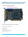
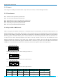
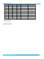
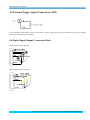
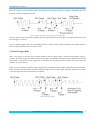
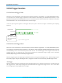
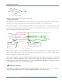
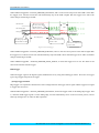
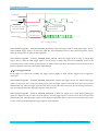
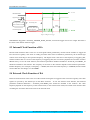
PCI8100
User’s Manual
Beijing ART Technology Development Co., Ltd.
PCI8100 Data Acquisition
Contents
Contents ................................................................................................................................................................................2
Chapter 1 Overview ..............................................................................................................................................................3
Chapter 2 Components Layout Diagram and a Brief Description .......................................................................................5
2.1 The Main Component Layout Diagram ..................................................................................................................5
2.2 The Function Description for the Main Component ...............................................................................................5
2.2.1 Signal Input and Output Connectors ............................................................................................................5
2.2.2 Jumper..........................................................................................................................................................6
2.2.3 Potentiometer ...............................................................................................................................................6
2.2.4 Physical ID of DIP Switch ...........................................................................................................................6
2.2.5 Status Indicator.............................................................................................................................................7
Chapter 3 Signal Connectors................................................................................................................................................8
Chapter4 Connection Ways for Each Signal.........................................................................................................................9
4.1 Analog Output Signal Connection ..........................................................................................................................9
4.2 External Clock Signal Input Connection.................................................................................................................9
4.3 Clock Signal Output Connection ............................................................................................................................9
4.4 External Trigger Signal Connection (DTR) ............................................................................................................9
4.5 External Trigger Signal Connection (ATR)...........................................................................................................10
4.6 Digital Input/Output Connection Mode ................................................................................................................10
Chapter 5 The Instruction of Trigger and Clock Functions ................................................................................................11
5.1 Trigger Mode ........................................................................................................................................................11
5.1.1 Single Trigger Mode ..................................................................................................................................11
5.1.2 Continuous Trigger Mode ..........................................................................................................................11
5.1.3 Stepped Trigger Mode................................................................................................................................11
5.1.4 Burst Trigger Mode ....................................................................................................................................12
5.2 DA Trigger Function .............................................................................................................................................13
5.2.1 DA Internal Trigger Mode..........................................................................................................................13
5.2.2 DA External Trigger Mode.........................................................................................................................13
5.3 Internal Clock Function of DA .............................................................................................................................17
5.4 External Clock Function of DA ............................................................................................................................17
Chapter 6 Notes, Calibration and Warranty Policy............................................................................................................18
6.1 Notes .....................................................................................................................................................................18
6.2 DA Analog Signal Output Calibration ..................................................................................................................18
6.3 Warranty Policy.....................................................................................................................................................18
Products Rapid Installation and Self-check ........................................................................................................................20
Rapid Installation ........................................................................................................................................................20
Self-check ...................................................................................................................................................................20
Delete Wrong Installation ...........................................................................................................................................20
BUY ONLINE at art-control.com/englishs or CALL+86-10-64862359/64861583(CN)
2
PCI8100 Data Acquisition
Chapter 1 Overview
In the fields of Real-time Signal Processing, Digital Image Processing and others, high-speed and high-precision data
acquisition modules are demanded. ART PCI8100 data acquisition module, which brings in advantages of similar
products that produced in china and other countries, is convenient for use and has low cost and stably high performance.
ART PCI8100 is an Arbitrary-waveform generator board based on PCI bus. It can be directly inserted into IBM-PC/AT
or a computer which is compatible with PCI8100. It can be used as signal generating source in a variety of fields such as
the laboratory, product quality testing center and so on.
Unpacking Checklist
Check the shipping carton for any damage. If the shipping carton and contents are damaged, notify the local dealer or
sales for a replacement. Retain the shipping carton and packing material for inspection by the dealer.
Check for the following items in the package. If there are any missing items, contact your local dealer or sales.
¾ PCI8100 Data Acquisition Board
¾ ART Disk
a) user’s manual (pdf)
b) drive
c) catalog
¾ Warranty Card
FEATURES
Analog Output
¾
¾
¾
¾
¾
¾
¾
¾
¾
¾
¾
¾
¾
¾
¾
¾
¾
Converter Type: DAC9765
Channel No.: 2-channel (synchronization)
Output Range: ±10V, ±5V
12-bit resolution
Dot Frequency: 1Hz~80MHz ( software configurable)
Frequency division formula= master frequency / the number of frequency division, the master frequency =80MHz,
32-bit frequency division, and the number of frequency division from 1 to 232.
High-speed mode (80MHz, only supports single-stage continuous output) and low-speed mode (5MHz and less)
Trigger Mode: single, continuous, single stepped and Burst trigger
Trigger Direction: negative, positive, either positive or negative trigger
Trigger Source: ATR (analog trigger) and DTR (digital trigger)
Trigger Source ATR Input Range: -10V~+10V
Trigger Level: -10V~+10V
Trigger Source DTR Input Range: standard TTL level
Clock Source: External Clock, Internal Clock (software-configurable)
Memory Depth: 512K words (points) RAM of each channel, it can be divided into 666 segments, looping for
arbitrary waveform generation
Data Transfer Mode: program mode
System Measurement Accuracy: 0.1%
Operating Temperature Range: 0℃~55℃
BUY ONLINE at art-control.com/englishs or CALL+86-10-64862359/64861583(CN)
3
PCI8100 Data Acquisition
¾
Storage Temperature Range: -20℃~70℃
Digital Input
¾
¾
¾
¾
Channel No.: 8-channel
Electric Standard: TTL compatible
High Voltage: ≧2V
Low Voltage: ≦0.8V
Digital Output
¾
¾
¾
¾
¾
¾
Channel No.: 8-channel
Electrical Standard: TTL compatible
High Voltage: ≧3.8V
Low Voltage: ≦0.44V
Power-on Reset
ge: high voltage≧2.4V, low voltage≦0.7V
Oscillation
Board Clock Oscillation: 80MHz
Dimension
130mm (L) * 99.5mm (W) * 16mm (H)
BUY ONLINE at art-control.com/englishs or CALL+86-10-64862359/64861583(CN)
4
PCI8100 Data Acquisition
Chapter 2 Components Layout Diagram and a Brief Description
2.1 The Main Component Layout Diagram
2.2 The Function Description for the Main Component
2.2.1 Signal Input and Output Connectors
CN1: analog output port 0.
CN2: analog output port 1.
CN3: ATR/DTR interface.
CN4: (CLKIN) external clock input interface
CN5: (CLKOUT) internal clock output interface
P1: digital input/output interface
BUY ONLINE at art-control.com/englishs or CALL+86-10-64862359/64861583(CN)
5
PCI8100 Data Acquisition
2.2.2 Jumper
JP1: CH3 port is ATR input interface when1-2 pin shorted, in contrast, it is the DTR input interface.
2.2.3 Potentiometer
RP1: AO0 full-scale adjustment potentiometer
RP2: AO1 full-scale adjustment potentiometer
RP3: ART trigger level zero-point adjustment potentiometer
RP4: ART trigger level full-scale adjustment potentiometer
RP5: AO0 zero-point adjustment potentiometer
RP6: AO1 zero-point adjustment potentiometer
2.2.4 Physical ID of DIP Switch
DID1: Set physical ID number. When the PC is installed more than one PCI8100 , you can use the DIP switch to set a
physical ID number for each board, which makes it very convenient for users to distinguish and visit each board in the
progress of the hardware configuration and software programming. The following four-place numbers are expressed by
the binary system: When DIP switch points to "ON", that means "1", and when it points to the other side, that means "0."
As they are shown in the following diagrams: place "ID3" is the high bit."ID0" is the low bit, and the black part in the
diagram represents the location of the switch. (Test software of the company often uses the logic ID management
equipments and at this moment the physical ID DIP switch is invalid. If you want to use more than one kind of the
equipments in one and the same system at the same time, please use the physical ID as much as possible.)
ON
ID3 ID2 ID1 ID0
ON
DID1
1
2
3
4
The above chart shows"1111", so it means that the physical ID is 15.
ON
ID3 ID2 ID1 ID0
ON
DID1
1
2
3
4
The above chart shows"0111", so it means that the physical ID is 7.
ON
ID3 ID2 ID1 ID0
ON
DID1
1
2
3
4
The above chart shows"0101", so it means that the physical ID is 5.
Physical ID(Hex) Physical ID(Dec)
ID3
ID2
ID1
ID0
OFF(0) OFF(0) OFF(0) OFF(0)
0
0
OFF(0) OFF(0) OFF(0) ON(1)
1
1
OFF(0) OFF(0) ON(1) OFF(0)
2
2
BUY ONLINE at art-control.com/englishs or CALL+86-10-64862359/64861583(CN)
6
PCI8100 Data Acquisition
OFF(0) OFF(0) ON(1)
3
3
OFF(0) ON(1)
OFF(0) ON(1)
ON(1)
OFF(0) OFF(0)
4
4
5
5
OFF(0) ON(1)
OFF(0) ON(1)
ON(1) OFF(0)
6
6
OFF(0) ON(1)
ON(1)
7
7
8
8
ON(1)
ON(1)
ON(1)
OFF(0) OFF(0) OFF(0)
9
9
ON(1)
OFF(0) OFF(0) ON(1)
OFF(0) ON(1) OFF(0)
A
10
ON(1)
OFF(0) ON(1)
B
11
ON(1)
ON(1)
ON(1)
OFF(0) OFF(0)
C
12
ON(1)
ON(1)
D
13
ON(1)
ON(1)
OFF(0) ON(1)
ON(1) OFF(0)
E
14
ON(1)
ON(1)
ON(1)
F
15
ON(1)
2.2.5 Status Indicator
LEDRAM1: RAM indicator
LEDRAM2: RAM indicator
BUY ONLINE at art-control.com/englishs or CALL+86-10-64862359/64861583(CN)
7
PCI8100 Data Acquisition
Chapter 3 Signal Connectors
20-pin P1 definition
DGND
1
2
DGND
DO7
3
4
DO6
DO5
5
6
DO4
DO3
7
DO2
DO1
9
8
10
DI7
11
12
DI6
DI5
13
14
DI4
DI3
15
16
DI2
DI1
17
18
DI0
+5VD
19
20
+5VD
DO0
Each pin function is defined in the table:
Pin Name
Pin Feature
Pin function definition
DI0-DI7
Input
Digital input, choose the DGND as reference ground.
DO0~DO7
Output
Digital output
+5VDC
Output
Output +5V power
DGND
GND
Digital ground
BUY ONLINE at art-control.com/englishs or CALL+86-10-64862359/64861583(CN)
8
PCI8100 Data Acquisition
Chapter4 Connection Ways for Each Signal
4.1 Analog Output Signal Connection
4.2 External Clock Signal Input Connection
4.3 Clock Signal Output Connection
4.4 External Trigger Signal Connection (DTR)
BUY ONLINE at art-control.com/englishs or CALL+86-10-64862359/64861583(CN)
9
PCI8100 Data Acquisition
4.5 External Trigger Signal Connection (ATR)
If use ART BNC down-lead to connect with output or input signals, please keep in mind that the red port is output/
input signals, the black port is ground.
4.6 Digital Input/Output Connection Mode
Digital signal input connection
Digital signal output connection
BUY ONLINE at art-control.com/englishs or CALL+86-10-64862359/64861583(CN)
10
PCI8100 Data Acquisition
Chapter 5 The Instruction of Trigger and Clock Functions
5.1 Trigger Mode
5.1.1 Single Trigger Mode
The waveform you define in the staging list is generated only once by going through the entire staging list. Only one
trigger is required to start the waveform generation.
Figure 5.1 uses the stages 0, 1, and 2 to illustrate a single trigger mode of operation for waveform generation mode.
After the PCI8100 receives a trigger, the waveform generation starts the first stage and continues through the last stage.
The last stage is generated repeatedly until you stop the waveform generation.
Figure 5.1 Single Trigger Mode
5.1.2 Continuous Trigger Mode
The waveform you define in the staging list is generated infinitely by continually cycling through the staging list. After
a trigger is received, the waveform generation starts at the first stage, continues through the last stage, and loops back
to the start of the first stage, continuing until you stop the waveform generation. Only one trigger is required to start the
waveform generation.
Figure 5.2 Continuous Trigger Mode for Arbitrary Waveform Generation Mode
5.1.3 Stepped Trigger Mode
After a start trigger is received, the waveform defined by the first stage is generated. Then, the device waits for the next
trigger signal. On the next trigger, the waveform described by the second stage is generated, and so on. Once the
staging list is exhausted, the waveform generation returns to the first stage and continues in a cyclic fashion.
Figure 5.3 uses the stages to illustrate a stepped trigger mode of operation for the Arbitrary Waveform Generation
BUY ONLINE at art-control.com/englishs or CALL+86-10-64862359/64861583(CN)
11
PCI8100 Data Acquisition
Mode. If a trigger is received while a stage is being generated, the trigger is ignored. A trigger is recognized only after
the stage has been completely generated.
Figure 5.3 The first eight samples of the next stage are generated repeatedly
After any stage has been generated completely, the first eight samples of the next stage are repeated continuously until
the next trigger is received.
Note: for stepped trigger mode, you can predefine the state in which a stage ends by making the first eight samples of
the next stage represent the state you want to settle.
5.1.4 Burst Trigger Mode
After a start trigger is received, the waveform defined by the first stage buffer is generated until another trigger is
received. At the next trigger, the buffer of the previous stage is completed before the waveform defined by the second
stage buffer is generated. Once the staging list is exhausted, the waveform generation returns to the first stage and
continues in a cyclic fashion.
Figure 5.4 uses the stages to illustrate a burst trigger mode of operation for the Arbitrary Waveform Generation Mode.
In this mode, the loop information associated with each stage is not used. The trigger causes the generation to proceed
to the next stage once the previous buffer is completed.
Figure 5.4 Burst Trigger Mode
BUY ONLINE at art-control.com/englishs or CALL+86-10-64862359/64861583(CN)
12
PCI8100 Data Acquisition
5.2 DA Trigger Function
5.2.1 DA Internal Trigger Mode
When DA is in the initialization, if the DA hardware parameter DAPara. TriggerMode = PCI8100_TRIGMODE_SOFT,
we can achieve the internal trigger acquisition. In this function, when calling the StartDeviceDA function, it will
generate DA start pulse, DA immediately access to the conversion process and not wait for the conditions of any other
external hardware. It also can be interpreted as the software trigger.
As for the specific process, please see the figure below, the cycle of the DA work pulse is decided by the sampling
frequency.
DA Start Pulse
The
first
working
pulse after the DA
start pulse
Figure 5.1 Internal Trigger Mode
5.2.2 DA External Trigger Mode
When DA is in the initialization, if the DA hardware parameter DAPara.TriggerMode = PCI8100_TRIGMODE_POST,
we can achieve the external trigger acquisition. In this function, when calling the StartDeviceProDA function, DA will
not immediately access to the conversion process but wait for the external trigger source signals accord with the
condition, then start converting the data. It also can be interpreted as the hardware trigger. Trigger source is the DTR
and ATR (Digital Trigger Source and Analog Trigger Source).
When the trigger signal is the digital signal (standard TTL-level), using the DTR trigger source. When the trigger signal
is the analog signal, using the ATR trigger source. (Trigger level needs to be set when using the ATR trigger source)
ATR Trigger
When the trigger signal is the analog signal, using the ATR trigger source. Trigger level needs to be set when using the
ATR trigger source, VO0’s output voltages of AO0 codetermines the trigger level, trigger level is -10V~+10V. There
are two trigger types: edge trigger and level trigger
BUY ONLINE at art-control.com/englishs or CALL+86-10-64862359/64861583(CN)
13
PCI8100 Data Acquisition
ATR
Result
Comparer
Trigger Level
Figure 5.2 Analog compare
The trigger modes include the edge trigger and level trigger.
(1) Edge trigger function
Edge trigger is to capture the characteristics of the changes between the trigger source signal and the trigger level signal
to trigger AD conversion. When TriggerType=PCI8100_TRIGTYPE_EDGE, it is the edge trigger type.
When ADPara.TriggerDir = PCI8100_TRIGDIR_NEGATIVE, choose the trigger mode as the falling edge trigger. That
is, when the ATR trigger signal is on the falling edge, AD will immediately access to the conversion process, and its
follow-up changes have no effect on AD acquisition.
AD Start Pulse
The first working pulse
AD Working Pulse
after triggered
Trigger Level
ATR
The waiting time
The
falling
edge
The first falling edge after the
before the AD started
AD started is valid
is invalid
Figure 5.3 Falling edge Trigger
When ADPara.TriggerDir = PCI8100_TRIGDIR_POSITIVE, choose the trigger mode as rising edge trigger. That is,
when the ATR trigger signal is on the rising edge, AD will immediately access to the conversion process, and its
follow-up changes have no effect on AD acquisition.
When ADPara.TriggerDir = PCI8100_TRIGDIR_POSIT_NEGAT, choose the trigger mode as rising or falling edge
trigger. That is, when the ATR trigger signal is on the rising or falling edge, AD will immediately access to the
conversion process, and its follow-up changes have no effect on AD acquisition. This function can be used in the case
that the acquisition will occur if the exoteric signal changes.
(2)Triggering level function
Level trigger is to capture the condition that trigger signal is higher or lower than the trigger level to trigger AD
conversion. When ADPara.TriggerType = PCI8100_TRIGTYPE_PULSE, it is level trigger type.
BUY ONLINE at art-control.com/englishs or CALL+86-10-64862359/64861583(CN)
14
PCI8100 Data Acquisition
When ADPara.TriggerDir = PCI8100_TRIGDIR_NEGATIVE, AD is in the conversion process if the ATR is lower than
the trigger level. And AD conversion will automatically stop if the ATR is higher than the trigger level. AD's work
status changes with changes of ATR.
AD Start Pulse
AD Working Pulse
The first pulse after
Pause
the AD triggered
mode
Analog Trigger Signal
Trigger Level
The waiting time
The falling edge before
The low level after the AD
the AD started is invalid
started is valid
The low level after the AD
started is valid
Figure 5.4 Low Level Trigger
When ADPara.TriggerDir = PCI8100_TRIGDIR_POSITIVE, AD is in the conversion process if the ATR is higher than
the trigger level. And AD conversion will automatically stop if the ATR is lower than the trigger level. AD's work status
changes with changes of ATR.
When ADPara.TriggerDir = PCI8100_TRIGDIR_POSIT_NEGAT, it means the trigger level is low. The effect is the
same as the internal software trigger.
DTR Trigger
When the trigger signal is the digital signal (standard TTL-level), using the DTR trigger source. There are two trigger
types: edge trigger and pulse level trigger.
(1) Edge trigger function
Edge trigger is to capture the characteristics of the changes between the trigger source signal and the trigger level signal
to trigger DA conversion.
When DAPara.TriggerDir = PCI8100_TRIGDIR_NEGATIVE, choose the trigger mode as the falling edge trigger. That
is, when the DTR trigger signal is on the falling edge, DA will immediately access to the conversion process, and its
follow-up changes have no effect on DA acquisition.
BUY ONLINE at art-control.com/englishs or CALL+86-10-64862359/64861583(CN)
15
PCI8100 Data Acquisition
DA Start Pulse
Digital Trigger Signal
The falling edge before
The waiting time
The first falling edge after the
the DA started is invalid
DA started is valid
The
DA Working Pulse
first
working
pulse after triggered
Figure 5.5 Falling edge Trigger
When DAPara.TriggerDir = PCI8100_TRIGDIR_POSITIVE, choose the trigger mode as rising edge trigger. That is,
when the DTR trigger signal is on the rising edge, DA will immediately access to the conversion process, and its
follow-up changes have no effect on DA acquisition.
When DAPara.TriggerDir = PCI8100_TRIGDIR_POSIT_NEGAT, choose the trigger mode as rising or falling edge
trigger. That is, when the DTR trigger signal is on the rising or falling edge, DA will immediately access to the
conversion process, and its follow-up changes have no effect on DA acquisition. This function can be used in the case
that the acquisition will occur if the exoteric signal changes.
(2)Level trigger function
Level trigger is to capture the condition that trigger signal is higher or lower than the trigger level to trigger DA
conversion.
When DAPara.TriggerDir = PCI8100_TRIGDIR_NEGATIVE, it means the trigger level is low. When DTR trigger
signal is in low level, DA is in the conversion process, once the trigger signal is in the high level, DA conversion will
automatically stop, when the trigger signal is in the low level again, DA will re-access to the conversion process that is,
only converting the data when the trigger signal is in the low level.
When DAPara.TriggerDir = PCI8100_TRIGDIR_POSITIVE, it means the trigger level is high. When DTR trigger
signal is in high level, DA is in the conversion process, once the trigger signal is in the low level, DA conversion will
automatically stop, when the trigger signal is in the high level again, DA will re-access to the conversion process, that
is, only converting the data when the trigger signal is in the high level.
BUY ONLINE at art-control.com/englishs or CALL+86-10-64862359/64861583(CN)
16
PCI8100 Data Acquisition
DA Start Pulse
Digital Trigger Signal
The high level before
The waiting time
the DA started is invalid
Pause
mode
The first pulse after
DA Working Pulse
the DA triggered
Figure 5.6 High Level Trigger
WhenDAPara.TriggerDir = PCI8100_TRIGDIR_POSIT_NEGAT, it means the trigger level is low or high. The effect is
the same as the internal software trigger.
5.3 Internal Clock Function of DA
Internal Clock Function refers to the use of clock signals which generated by on-board clock oscillator to trigger the
DA conversion regularly. The clock of reading waveform data stored in SRAM is produced by the on-board logic
control circuit according to user-specified frequency. The largest clock is the same as the frequency of triggering DA,
and the smallest clock is 1/65535 of the frequency of triggering DA, this can achieve playback the waveform stored in
SRAM slowly. To use the clock function, the hardware parameters DAPara.ClockSouce =PCI8100_CLOCKSRC_IN
should be installed in the software. The frequency of the clock in the software depends on the hardware parameters.
DAPara.Frequency. For example, if Frequency = 100000, that means AD work frequency is 100000Hz, but the refresh
clock of DA does not change, it is still 40MHz.
5.4 External Clock Function of DA
External Clock Function refers to the use of the outside clock signals to trigger the DA conversion regularly. The clock
signals are provide by the INCLK pin of the BNC connector.
To use the external clock function, the hardware
parameters DAPara.ClockSouce = PCI8100_CLOCKSRC_OUT should be installed in the software. The clock
frequency depends on the frequency of the external clock, in the external clock mode, DA refresh clock and the clock
of reading the waveform data are the same as the external clock.
BUY ONLINE at art-control.com/englishs or CALL+86-10-64862359/64861583(CN)
17
PCI8100 Data Acquisition
Chapter 6 Notes, Calibration and Warranty Policy
6.1 Notes
In our products’ packing, user can find a user manual, a PCI8100 module and a quality guarantee card. Users must
keep quality guarantee card carefully, if the products have some problems and need repairing, please send products
together with quality guarantee card to ART, we will provide good after-sale service and solve the problem as quickly
as we can.
When using PCI8100, in order to prevent the IC (chip) from electrostatic harm, please do not touch IC (chip) in the
front panel of PCI8100 module.
6.2 DA Analog Signal Output Calibration
Every device has to be calibrated before sending from the factory. It is necessary to calibrate the module again if users
want to after using for a period of time or changing the input range. PCI8100 output range: ±10V.
1) Connect the ground of the digital voltage meter to any analog AGND. Connect the input side of the voltage
meter to the output channel which needs calibration. Run PCH2001 test procedure under Windows, select the
AO output detection.
2) To set output 2048, adjust potentiometer RP5/RP6 in order to make AO0/AO1 output 0.000V.
3) To set output 4095, adjust potentiometer RP1/RP2 in order to make AO0/AO1 output 10.000V.
4) Repeat steps above until meet the requirement.
6.3 Warranty Policy
Thank you for choosing ART. To understand your rights and enjoy all the after-sales services we offer, please read the
following carefully.
1. Before using ART products please read the user manual and follow the instructions exactly. When sending in
damaged products for repair, please attach an RMA application form which can be downloaded from:
www.art-control.com.
2. All ART products come with a limited two-year warranty:
¾ The warranty period starts on the day the product is shipped from ART factory
¾ For products containing storage devices (hard drives, flash cards, etc.), please back up your data before sending
them for repair. ART is not responsible for any loss of data.
¾ Please ensure the use of properly licensed software with our systems. ART does not condone the use of pirated
software and will not service systems using such software. ART will not be held legally responsible for products
shipped with unlicensed software installed by the user.
3. Our repair service is not covered by ART guarantee in the following situations:
¾ Damage caused by not following instructions in the User's Manual.
¾ Damage caused by carelessness on the user's part during product transportation.
¾ Damage caused by unsuitable storage environments (i.e. high temperatures, high humidity, or volatile chemicals).
BUY ONLINE at art-control.com/englishs or CALL+86-10-64862359/64861583(CN)
18
PCI8100 Data Acquisition
¾ Damage from improper repair by unauthorized ART technicians.
¾ Products with altered and/or damaged serial numbers are not entitled to our service.
4. Customers are responsible for shipping costs to transport damaged products to our company or sales office.
5. To ensure the speed and quality of product repair, please download an RMA application form from our company
website.
BUY ONLINE at art-control.com/englishs or CALL+86-10-64862359/64861583(CN)
19
PCI8100 Data Acquisition
Products Rapid Installation and Self-check
Rapid Installation
Product-driven procedure is the operating system adaptive installation mode. After inserting the disc, you can select the
appropriate board type on the pop-up interface, click the button【driver installation】; or select CD-ROM drive in
Resource Explorer, locate the product catalog and enter into the APP folder, and implement Setup.exe file. After the
installation, pop-up CD-ROM, shut off your computer, insert the PCI card. If it is a USB product, it can be directly
inserted into the device. When the system prompts that it finds a new hardware, you do not specify a drive path, the
operating system can automatically look up it from the system directory, and then you can complete the installation.
Self-check
At this moment, there should be installation information of the installed device in the Device Manager (when the
device does not work, you can check this item.). Open "Start -> Programs -> ART Demonstration Monitoring and
Control System -> Corresponding Board -> Advanced Testing Presentation System", the program is a standard testing
procedure. Based on the specification of Pin definition, connect the signal acquisition data and test whether AD is
normal or not. Connect the input pins to the corresponding output pins and use the testing procedure to test whether the
switch is normal or not.
Delete Wrong Installation
When you select the wrong drive, or viruses lead to driver error, you can carry out the following operations: In
Resource Explorer, open CD-ROM drive, run Others-> SUPPORT-> PCI.bat procedures, and delete the hardware
information that relevant to our boards, and then carry out the process of section I all over again, we can complete the
new installation.
BUY ONLINE at art-control.com/englishs or CALL+86-10-64862359/64861583(CN)
20