1
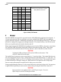
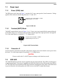
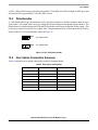
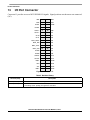
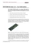
Freescale Semiconductor
Document Number: M5211DEMO
Rev. 1, 04/2007
Demonstration Board for
Freescale MCF5211
1
Overview
The M5211DEMO is a low-cost development system for
the Freescale MCF5211 ColdFire® microcontroller.
Application development is quick and easy with the
included DB9 serial cable and integrated BDM. The
integrated BDM is compatible with popular hosting
software and allows easy application development and
debugging. An optional BDM port compatible with
standard ColdFire BDM / JTAG interface cables and
hosting software is provided but not installed.
© Freescale Semiconductor, Inc., 2007. All rights reserved.
Contents
1
2
3
4
5
6
7
8
9
10
11
12
13
Overview . . . . . . . . . . . . . . . . . . . . . . . . . . . . . . . . . . . . . 1
Getting Started . . . . . . . . . . . . . . . . . . . . . . . . . . . . . . . . 5
Software Development . . . . . . . . . . . . . . . . . . . . . . . . . . 5
Operating Modes . . . . . . . . . . . . . . . . . . . . . . . . . . . . . . . 5
Memory Map . . . . . . . . . . . . . . . . . . . . . . . . . . . . . . . . . . 6
Development Support . . . . . . . . . . . . . . . . . . . . . . . . . . . 7
Power . . . . . . . . . . . . . . . . . . . . . . . . . . . . . . . . . . . . . . . 8
Reset . . . . . . . . . . . . . . . . . . . . . . . . . . . . . . . . . . . . . . . 11
Low-Power Modes. . . . . . . . . . . . . . . . . . . . . . . . . . . . . 12
Timing . . . . . . . . . . . . . . . . . . . . . . . . . . . . . . . . . . . . . . 12
Communications . . . . . . . . . . . . . . . . . . . . . . . . . . . . . . 13
User Options . . . . . . . . . . . . . . . . . . . . . . . . . . . . . . . . . 14
I/O Port Connector. . . . . . . . . . . . . . . . . . . . . . . . . . . . . 16
Overview
Figure 1. M5211DEMO Board
1.1
•
•
•
•
Features
MCF5211 CPU, 64 pins
— 128 byte flash
— 16K byte RAM
— 2K byte cache RAM
— DMA controller with timers
— Interrupt controller
— Eight channel 12 bit A/D
— QSPI, IIC, and CAN serial ports
— 1 x UART Serial Ports with DMA capability
— Edge / interrupt port
— Eight PWM timers
— Four GPT timers
— BDM / JTAG port
— 3.3 V operation
— 66 MHz bus
40 pin I/O port
Integrated USB BDM port
BDM / JTAG port, 26 pins, development port (not installed)
Demonstration Board for Freescale MCF5211, Rev. 1
2
Freescale Semiconductor
Overview
•
•
•
•
•
•
•
•
•
•
1.2
•
•
•
RS-232 serial port with DB9-S connector
Timing options
— Internal oscillator, 8 MHz
— External XTAL option (not installed)
— External clock options (not installed)
RESET switch with indicator
ON/OFF Power Switch w/ LED indicator
Power input selection jumper
— Power input from USB BDM
— Power input from on-board, +3.3 V, regulator
— Power input from terminal block
— Power from connector J1
— Optional power output through connector J1
User features
— Four user LEDs with enable jumper
— Two user push switches
— 5 kΩ POT with enable jumper
Option jumpers
— Power input select
— Optional power output Enable
— BDM_EN
— XTAL_EN
— POT_EN
— COM_EN
— LED_EN
Connectors
— DB9 serial connector
— Type B USB connector
— 2.0 mm barrel power input
— 2 pos, screw type, terminal block
Supplied with DB9 serial cable, USB cable, utility / support CD
Manuals and wall adapter power supply.
Specifications
Board size: 3.5" x 5.5"
Power input: +5 to +20 VDC, 9 VDC typical
Current consumption: 100 mA typical at 9 VDC input
Demonstration Board for Freescale MCF5211, Rev. 1
Freescale Semiconductor
3
Overview
1.3
Reference Documents
Table 1 shows a list of reference documents that are provided on the support CD in Adobe Portable
Document Format (PDF).
Table 1. Reference Documents
File name
1.4
Document Description
M5211DEEMO_UG.pdf
M5211DEMO User Guide (this document)
M5211DEMO_SCH_E.pdf
M5211DEMO Schematic, Rev E
M5211DEMO_QSG.pdf
M5211DEMO Quick Start Guide
M5211DEMO_example1.zip
CodeWarrior Demo Application
M5211DEMO_example2.zip
CodeWarrior Demo Application
MCF5213RM.pdf
MCF5213 Reference Manual
MCF5213DE.pdf
MCF5213 Device Errata
Cautionary Notes
Electrostatic discharge (ESD) prevention measures must be used when handling this product. ESD
damage is not a warranty repair item.
The manufacturer of this board, Axiom Manufacturing, does not assume any liability arising out of the
application or use of any product or circuit described herein; neither does it convey any license under
patent rights or the rights of others.
1.4.1
EMC Information on the M5211DEMO board
This product is shipped from the factory with associated power supplies and cables, and has been verified
to meet with requirements FCC as a CLASS A product.
This product is designed and intended for use as a development platform for hardware or software in an
educational or professional laboratory.
In a domestic environment, this product may cause radio interference in which case you may be required
to take adequate prevention measures.
Attaching additional wiring to this product or modifying the product operation from the factory default as
shipped may effect its performance and cause interference with other apparatus in the immediate vicinity.
If such interference is detected, suitable mitigating measures must be taken.
1.5
Terminology
This development board uses option selection jumpers. A jumper is a plastic shunt that connects
two terminals electrically. Terminology for application of the option jumpers is as follows:
• Jumper on, in, or installed—jumper is installed such that two pins are connected.
• Jumper off, out, or idle— jumper is installed on one pin only. It is recommended that jumpers be
idled by installing on 1 pin so they will not be lost.
Demonstration Board for Freescale MCF5211, Rev. 1
4
Freescale Semiconductor
Getting Started
2
Getting Started
To get started, please refer to the M5211 Quick Start Guide included with this development kit.
The M5211DEMO single board computer is a fully assembled, fully functional development board for the
Freescale MCF5211 microcontroller. An included serial cable, USB cable, and support software allows
you to get started quickly.
The purpose of this development board is to assist you in quickly developing an application in a known
working environment, to provide an evaluation platform, or as a control module for an embedded system.
You should be familiar with memory mapping, memory types, and embedded software design for
successful application development.
You should be familiar with the hardware and software operation of the target MCF5211 device before
beginning. If necessary, refer to the MCF5213 Integrated Microcontroller Reference Manual, included on
the support CD, for details on the operation of the MCF5211.
3
Software Development
Software development requires the use of a ColdFire assembler or compiler and a host PC running a
ColdFire BDM interface. CodeWarrior 6.1 Special Edition, which is supplied with this board, allows you
to develop and debug application code and to program the flash memory.
To ensure successful application development, load and execute the application from RAM. After the
application has been completely debugged fully functional, it can be ported to flash memory. When
programmed into flash memory, the application will execute from power-on or RESET.
4
Operating Modes
The M5211DEMO board operates in two basic modes RUN mode, or DEBUG mode. RUN mode executes
user application code from power-on or reset. DEBUG mode supports the development and debug of
applications via the integrated USB BDM. An optional BDM_PORT is provided but not installed. See
the related sections below for quickly starting the board in the desired mode of operation.
The board has been preloaded with a demonstration program that operates in the RUN mode (see the
M5211DEMO Quick Start Guide for additional information). The VDD LED is lit when power is applied
to the board and the PWR_SEL option header is set correctly. The OFF/ON switch must also be set to the
ON position.
4.1
RUN Mode
RUN mode allows your application to execute out of flash memory when power is applied to the board or
the RESET button is pressed. Use these settings to configure the M5211DEMO board for RUN mode
using the USB bus to power the board. See tSection 7, “Power,” for details on configuring the board for
alternate power input.
1. Connect a serial cable between the board and a host PC if needed.
2. Connect auxiliary equipment to board if needed.
3. Configure the board option jumpers as shown in Table 2.
Demonstration Board for Freescale MCF5211, Rev. 1
Freescale Semiconductor
5
Memory Map
Table 2. Run Mode Setup
PWR_SEL
Set to VB
BDM_EN
OFF
COM_EN
ALL ON (if required)
VX_EN
ON (if required)
Connect the USB cable to an open USB port on the host PC and attach to the USB port on the target board.
LED's 1–4 located adjacent to the DB-9 connector, and the VDD LED will light and the loaded application
will begin to execute.
4.2
DEBUG Mode
DEBUG mode supports application development and debug using the ColdFire background debug mode
(BDM). Background mode is accessible using either the integrated USB-BDM or an external ColdFire
BDM cable. Use of the integrated BDM requires a host PC with an available USB port and an A/B USB
cable and appropriate hosting software. The USB cable used must be USB 2.0 compliant. A 26-pin
BDM_PORT header supports the use of an external BDM cable. This header is not installed in default
configurations. The steps describe using the integrated USB-BDM. See Section 7, “Power,” for details
on configuring the board for alternate power input.
1. Connect a serial cable between the board and a host PC if needed.
2. Connect auxiliary equipment to board if needed.
3. Install and launch CodeWarrior™ 6.1 Special Edition, or other software capable of communicating
with the ColdFire MCU.
4. Configure the board option jumpers as shown in Table 3.
Table 3. Debug Mode Setup
PWR_SEL
Set to VB
BDM_EN
ON
COM_EN
ALL ON (if required)
VX_EN
ON (if required)
Connect the supplied USB cable between an available USB port on the host PC and the USB connector on
the board.
Hosting development software will establish background communication.
5
Memory Map
Refer to the MCF5213 Integrated Microcontroller Reference Manual for details.
Demonstration Board for Freescale MCF5211, Rev. 1
6
Freescale Semiconductor
Development Support
6
Development Support
Application development and debug for the target MCF5211 is supported through the BDM interface. The
debug interface consists of an integrated USB-BDM debugger and an optional 26-pin header
(BDM_PORT). The BDM_PORT header is not installed in default configuration, but you may install it if
needed.
6.1
Integrated BDM_PORT
The M5211DEMO board features an integrated USB-BDM debugger from P&E Microcomputer Systems.
The integrated debugger supports application development and debugging via the background debug
mode. A USB, type B, connector provides connectivity between the target board to the host PC.
The integrated debugger provides power and ground to the target, thereby eliminating the need to power
the board externally. When used, power from the USB-BDM circuit is derived from the USB bus and total
current consumption is limited by the USB specification. Total current consumption for the target board,
and all connected circuitry, must not exceed 500 mA. Excessive current drain will violate the USB
specification causing the bus to disconnect. This forces a target POR.
CAUTION
Violating the USB specification will cause the USB bus to disconnect
forcing the target to reset.
Use of the integrated USB BDM requires the use of CodeWarrior 6.1 Special Edition or development tools
from P&E Microcomputer Systems.
6.2
BDM_PORT Header
A ColdFire BDM cable may be attached to the 26-pin BDM_PORT port header. This header is not
installed in default configuration and its use requires you to install a 2x13, 0.1" center, BERG header.
Refer to the BDM documentation in the MCF5213 User's Manual for details on the use of the BDM cable.
The BDM_PORT header pin-out is shown in Figure 2.
Demonstration Board for Freescale MCF5211, Rev. 1
Freescale Semiconductor
7
Power
NC
1
2
BKPT*
GND
3
4
DSCLK
GND
5
6
TCLK (JTAG)
RSTI*
7
8
DSI
VDD
9
10
DSO
GND
11
12
ALLPST
ALLPST
13
14
ALLPST
ALLPST
15
16
NC
NC
17
18
NC
NC
19
20
GND
NC
21
22
NC
GND
23
24
TCLK (BDM)
VDD
25
26
TA*
See the ColdFire BDM chapter in the
MCF5213 User's Manual for complete
BDM_PORT documentation.
Note: This header is not installed in default configuration.
Figure 2. BDM_PORT Header
7
Power
The M5211DEMO is designed to be powered from the USB_BDM during application development. A
2.0 mm barrel connector and a two-position, screw-type, terminal block (BATT) has been applied to
support stand-alone operation. Additionally, the board may be powered through connector J1. The board
may also be configured to supply power through connector J1 to external circuitry. An OFF/ON switch
allows you to quickly and easily turn the board on and off.
When using the integrated USB-BDM, the board draws power from the USB bus. Excessive current drain
will violate the USB specification causing the USB bus to disconnect forcing a POR. Total current
consumption of the board and connected circuitry, therefore, must be limited to less than 500 mA.
CAUTION
Violating the USB specification will cause the USB bus to disconnect. This
will force a hard reset on the target.
The installed barrel connector accepts a center-positive, 2.1 mm barrel plug. The terminal block accepts
wire sizes ranging from 28 ga to 16 ga. Voltage input must be in the range between +5 V and +20 V. At
no time should input voltage exceed +20 V as damage to the board may result. The terminal block input
is connected directly to the upper voltage rail. Input protection is not applied on this voltage input.
Exercise caution when using the terminal block to input power to the board.
Voltage supplied through connector J1 is also connected directly to the board voltage rails. No protection
is applied on this input and you must exercise caution when powering the board from connector J1.
CAUTION
Input protection is not applied to the J1 or BATT power inputs. Excessive
input voltage or current will damage the board.
Demonstration Board for Freescale MCF5211, Rev. 1
8
Freescale Semiconductor
Power
7.1
7.1.1
Power Input
Power (PWR) Jack
The PWR power jack, shown in Figure 3, consists of a 2.1 mm, center-positive, barrel connector. Voltage
applied at this connector should range between +5 V and +20 V.
2.0 mm–2.1 mm, center-positive, +V input
Applied voltage: +5 V – +20 V
PWR
Figure 3. PWR Jack
7.1.2
Terminal (BATT) Block
The BATT terminal block, shown in Figure 4, is a 3.5 mm, screw-type terminal block connected directly
to the VDD voltage rail. Caution must be used when using this input since input protection is not applied.
Use of this input requires a regulated +3.3 V voltage source.
Accepts wire size 28 AWG – 16 AWG
Applied voltage must be +3.3 V.
+
BATT
-
Figure 4. BATT Terminal Block
7.1.3
Connector J1
See the schematic for details on using this connection to supply power to the board or source power from
the board. Use of this input requires a regulated +3.3 V voltage source.
CAUTION
Do not overdrive the J1 or BATT inputs as damage to the board may result.
7.2
VDD LED
The VDD LED indicates the state of power applied to the development board. This LED is on when power
is applied to the board. If no power is applied or the OFF/ON switch is in the OFF position, this LED be
off. The VDD LED is located after the OFF/ON switch and will indicate the state of the switch if the board
is powered from the on-board regulator, the USB circuit, or the BATT terminal block input.
Demonstration Board for Freescale MCF5211, Rev. 1
Freescale Semiconductor
9
Power
7.3
Power (OFF/ON) Switch
The OFF/ON switch, shown in Figure 5, connects and disconnects all input voltage sources to the board.
In the OFF position, the board is unpowered and no voltage is present on the upper voltage rail. In the ON
position, the input voltage source is connected to the upper voltage rail.
OFF/ON
CONFIGURATION
OFF—Input power source disconnected from upper voltage rail
OFF/ON
ON—Input power source connected to upper voltage rail
Figure 5. OFF/ON Switch
7.4
Power Select
Configuration of applied input power is controlled using two option headers. The PWR_SEL header
selects between the on-board voltage regulator and the USB voltage input. The VX_EN header connects
J1-1 directly to the upper voltage rail. The illustrations below show the different configuration for each
option header.
7.4.1
PWR_SEL
Figure 6 shows the PWR_SEL header.
Select power input from USB-BDM
VB
VDD
PWR_SEL
Select power input from VR1
VB
VDD
PWR_SEL
Figure 6. PWR_SEL Option Header
Power from the integrated BDM is drawn from the USB bus and is limited to 500 mA. Excessive current
drain will violate the USB specification causing the USB bus to disconnect.
CAUTION
Violating the USB specification will cause the USB bus to disconnect. This
will cause the board to reset.
The on-board voltage regulator (VR1) accepts power input through a 2.1 mm barrel connector (PWR).
Input voltage may range from +5 V to +20 V. VR1 provides a +3.3 V fixed output limited to 800 mA.
Over-temperature and over-current limit built into the voltage regulator provides limited protection from
damage due to excessive stresses.
Demonstration Board for Freescale MCF5211, Rev. 1
10
Freescale Semiconductor
Reset
Consider the maximum output current of the selected power source when attempting to power off-board
circuitry through connector J1.
7.4.2
VX_EN
The VX_EN option header is a two-pin jumper that connects the target-board voltage rail to J1-1. J1-3 is
connected directly to the ground plane. Use of this input requires a regulated +3.3 V voltage source. This
power input is decoupled to minimize noise input but is not regulated. Also, no protection is applied on
this input and damage to the target board may result if over-driven. Do not attempt to power the target
board through this connector while applying power through the USB-BDM or the PWR connector;
damage to the board may result.
Power may be sourced to off-board circuitry through the J1 connector. The current limitation of the USB
bus or the on-board regulator must be considered when attempting to source power to external circuitry.
Excessive current drain may damage the target board, the host PC USB hub, or the on-board regulator.
Figure 7 details the VX_EN option header connections.
ON
Enable power connection to connector J1
OFF
Disable power connection to connector J1
VX_EN
VX_EN
Figure 7. VX_EN Option Header
CAUTION
Do not apply power to connector J1 while sourcing power from either the
PWR connector or the USB-BDM circuit. Damage to the board may result.
NOTE
Do not exceed available current supply from USB-BDM cable or on-board
regulator when sourcing power through connector J1 to external circuitry.
8
Reset
The MCF5211 can be reset several ways. A RESET switch applies an external reset to the device. An
internal low-voltage detect forces the part into RESET when voltage falls too low. The part may also be
reset by applying a logic low on the RSTI* signal. The RSTI* signal is used by a connected BDM to force
the part into reset when necessary. A reset indicator shows when the part is in reset.
8.1
Reset Switch
The RESET switch provides a method to apply an asynchronous reset to the MCU and is connected
directly to the RSTI* input on the MCU. Pressing the RESET switch forces the MCU into reset until the
Demonstration Board for Freescale MCF5211, Rev. 1
Freescale Semiconductor
11
Low-Power Modes
switch is released. An external pullup on the RSTI* line prevents spurious resets and allowing normal
operation.
8.2
Low-Voltage Detect
The MCF5211 utilizes an internal Low-Voltage Detect (LVD) to protect against under-voltage conditions.
The LVD is enabled out of RESET. Consult the MCF5213 Integrated Microcontroller Reference Manual
for details on configuring LVD operation.
8.3
Reset Indicator
The RESET LED turns on when the MCU is in RESET and remains on for the duration of a valid RSTO*
signal.
9
Low-Power Modes
The MCF5211 supports several operational modes designed to reduce power consumption. Low-power
modes include Wait, Doze, Stop, and Halt. Refer to the MCF5213 Microcontroller Family Hardware
Specification and the MCF5213 Integrated Microcontroller Reference Manual for details on configuring
and using the various low-power modes.
10
Timing
Timing for the M5211DEMO is provided by an on-chip, 8 MHz relaxation oscillator in default
configuration. Resistor R23 causes the MCU to select the internal oscillator as the timing source out of
reset. Refer to the M5213 Integrated Microcontroller Reference Manual for details on use and
configuration of internal timing.
Pad locations for an external crystal oscillator have been provided but not populated in default
configurations. The external oscillator is connected to the XTAL and EXTAL inputs. To implement an
external crystal oscillator simply remove R23, install the oscillator and related circuitry. The XTAL_EN
shunt must be installed to enable external timing operation.
ON
Enables external crystal oscillator input to MCU
OFF
Disables external crystal oscillator input to MCU
XTAL_EN
XTAL_EN
Figure 8. OSC_EN Option Header
Pad locations for an optional 32.768 kHz have also been provided but not populated. The 32.768 kHz
timing input is connected to GPT0 and GPT1 inputs. To implement this timing input, simply install the
timing source and related circuitry.
Demonstration Board for Freescale MCF5211, Rev. 1
12
Freescale Semiconductor
Communications
11
Communications
The M5211DEMO board provides two Serial Communications Interface (SCI) ports, one Serial Peripheral
Interface (SPI) port, and one Inter-Integrated Controller (IIC) port. RS-232 communications are supported
through a DB9 connector and connector J1. SPI and IIC communications are supported through connector
J1. The COM_EN option header enables SCI0 operation on the board.
11.1
SCI Port
An RS-232 transceiver provides RS-232 to TTL/CMOS logic-level translation between the COM
connector and the MCU. The COM connector is a 9-pin Dsub, right-angle connector. A ferrite bead on
shield ground provides conducted immunity protection. Communication signals TXD0 and RXD0 are
routed from the transceiver to the MCU. These signals are also available on connector J1. Hardware flow
control signals RTS0 and CTS0are also routed from the transceiver to the MCU.
Serial communications signals RXD1, TXD1, RTS1, and CTS1 are available on connector J1 and route
directly between the MCU and connector J1. The SCI1 port does not have a RS-232 logic-level translation.
11.2
COM_EN
The COM_EN option header (Figure 9) individually connects and disconnects SCI0 signals between the
MCU and the SCI transceiver. Removing a shunt disconnects the associated signal. Installing a shunt
connects the associated signal.
Shunt
COM_EN
On
Off
CTS
Enabled
Disabled
RTS
Enabled
Disabled
RXD
Enabled
Disabled
TXD
Enabled
Disabled
Figure 9. COM_EN Option Header
11.2.1
COM Connector
A standard 9-pin Dsub connector provides external connections for the SCI0 port. The Dsub shell is
connected to board ground through a ferrite bead. The ferrite bead provides noise isolation on the RS-232
connection. The DB9 connector pinout is shown in Figure 10.
Demonstration Board for Freescale MCF5211, Rev. 1
Freescale Semiconductor
13
User Options
4, 6
1
TXD
2
RXD
3
1, 6
4
GND
5
6
1, 4
Female DB9 connector that interfaces to the ColdFire
internal SCI1 serial port via the RS232 transceiver.
7
RTS
Pins 1, 4, and 6 are connected together.
8
CTS
9
NC
Figure 10. COM Connector
11.3
SPI Port
SPI signaling connects directly between connector J1 and the MCU. Refer to the MCF5213 Integrated
Microcontroller Reference Manual for details on using the SPI interface.
11.4
IIC Port
IIC signaling connects directly between connector J1 and the MCU. Refer to the MCF5213 Integrated
Microcontroller Reference Manual for details on using the IIC interface.
12
User Options
The M5211DEMO includes various input and output devices to aid application development. User I/O
devices include two momentary pushbutton switches, four green LEDs, and one potentiometer.
12.1
Pushbutton Switches
Two pushbutton switches provide momentary, active-low input, for user applications. Pull-ups internal to
the MCU must be enabled to provide error free switch operation. Pushbutton switches SW1 and SW2 are
connected to MCU I/O ports IRQ4* and IRQ7* respectively.
12.2
LED Indicators
Indicators LED1 through LED4 are enabled by the LED_EN option header, shown in Figure 11. Each
LED is active-high and illuminates when a logic high signal is driven from the respective MCU I/O port.
A 3S buffer between the MCU port and the user LEDs provides the drive current necessary to control the
LEDs.
LED_EN
ON
User LEDs enabled active-high
OFF
User LEDs disabled
LED_EN
Figure 11. LED_EN Option Header
Demonstration Board for Freescale MCF5211, Rev. 1
14
Freescale Semiconductor
User Options
A SW2_LED pad has been provided but not installed. If installed, this LED will light on SW2 press and
will remain lit for approximately 2 ms after SW2 release.
12.3
Potentiometer
A 5 kΩ, thumb-wheel type, potentiometer at RV1 provides continuous, variable resistance input for user
applications. The output is the result of a voltage divider that changes as the thumb-wheel is turned. The
potentiometer is connected between VDD and GND with the center tap providing the divider output. This
center tap is connected to the MCU on signal AN0. The potentiometer may be disconnected from AN0 by
means of the POT_EN option header, shown in Figure 12.
ON
User POT enabled
OFF
User POT disabled
POT_EN
POT_EN
Figure 12. POT_EN Option Header
12.4
User Option Connection Summary
Table 4 summarizes user option connections on the development board.
Table 4. User Option Connections
Option
MCU Port
MCU Pin
SW1
IRQ4
57
SW2
IRQ7
58
LED1
DTIN0
22
LED2
DTIN1
23
LED3
DTIN2
18
LED4
DTIN3
19
RV1
AN0
25
Demonstration Board for Freescale MCF5211, Rev. 1
Freescale Semiconductor
15
I/O Port Connector
13
I/O Port Connector
Connector J1 provides access to M5211DEMO I/O signals. Signal positions not shown are not connected
(NC).
VDD
1
2
IRQ1*
GND
3
4
RSTI*
UTXD1
5
6
RSTO*
URXD1
7
8
URTS1*
9
10
ANO
UCTS1*
11
12
AN1
GPT0
13
14
AN2
GPT1
15
16
AN3
QSPI_DOUT
17
18
AN4
QSPI_DIN
19
20
AN5
QSPI_SCLK
21
22
AN6
QSPI_CS0
23
24
AN7
UTXD0
25
26
SCL
TRXD0
27
28
SDA
URTS0*
29
30
GPT2
UCTS0*
31
32
GPT3
IRQ4*
33
34
DTIN0
VRH
35
36
DTIN1
VRL
37
38
DTIN2
IRQ7*
39
40
DTIN3
Figure 13. Connector J1
Table 5. Revision History
Revision (Date)
Description
A (01/2006)
Initial release as Axiom Manufacturing document.
1 (04/2007)
• Converted document to Freescale identity and standards.
• Formatting, layout, spelling, and grammar corrections.
Demonstration Board for Freescale MCF5211, Rev. 1
16
Freescale Semiconductor
THIS PAGE IS INTENTIONALLY BLANK
Demonstration Board for Freescale MCF5211, Rev. 1
Freescale Semiconductor
17
How to Reach Us:
Home Page:
www.freescale.com
Web Support:
http://www.freescale.com/support
USA/Europe or Locations Not Listed:
Freescale Semiconductor, Inc.
Technical Information Center, EL516
2100 East Elliot Road
Tempe, Arizona 85284
+1-800-521-6274 or +1-480-768-2130
www.freescale.com/support
Europe, Middle East, and Africa:
Freescale Halbleiter Deutschland GmbH
Technical Information Center
Schatzbogen 7
81829 Muenchen, Germany
+44 1296 380 456 (English)
+46 8 52200080 (English)
+49 89 92103 559 (German)
+33 1 69 35 48 48 (French)
www.freescale.com/support
Japan:
Freescale Semiconductor Japan Ltd.
Headquarters
ARCO Tower 15F
1-8-1, Shimo-Meguro, Meguro-ku,
Tokyo 153-0064
Japan
0120 191014 or +81 3 5437 9125
[email protected]
Asia/Pacific:
Freescale Semiconductor Hong Kong Ltd.
Technical Information Center
2 Dai King Street
Tai Po Industrial Estate
Tai Po, N.T., Hong Kong
+800 2666 8080
[email protected]
For Literature Requests Only:
Freescale Semiconductor Literature Distribution Center
P.O. Box 5405
Denver, Colorado 80217
1-800-441-2447 or 303-675-2140
Fax: 303-675-2150
[email protected]
Document Number: M5211DEMO
Rev. 1
04/2007
Information in this document is provided solely to enable system and software
implementers to use Freescale Semiconductor products. There are no express or
implied copyright licenses granted hereunder to design or fabricate any integrated
circuits or integrated circuits based on the information in this document.
Freescale Semiconductor reserves the right to make changes without further notice to
any products herein. Freescale Semiconductor makes no warranty, representation or
guarantee regarding the suitability of its products for any particular purpose, nor does
Freescale Semiconductor assume any liability arising out of the application or use of any
product or circuit, and specifically disclaims any and all liability, including without
limitation consequential or incidental damages. “Typical” parameters that may be
provided in Freescale Semiconductor data sheets and/or specifications can and do vary
in different applications and actual performance may vary over time. All operating
parameters, including “Typicals”, must be validated for each customer application by
customer’s technical experts. Freescale Semiconductor does not convey any license
under its patent rights nor the rights of others. Freescale Semiconductor products are
not designed, intended, or authorized for use as components in systems intended for
surgical implant into the body, or other applications intended to support or sustain life,
or for any other application in which the failure of the Freescale Semiconductor product
could create a situation where personal injury or death may occur. Should Buyer
purchase or use Freescale Semiconductor products for any such unintended or
unauthorized application, Buyer shall indemnify and hold Freescale Semiconductor and
its officers, employees, subsidiaries, affiliates, and distributors harmless against all
claims, costs, damages, and expenses, and reasonable attorney fees arising out of,
directly or indirectly, any claim of personal injury or death associated with such
unintended or unauthorized use, even if such claim alleges that Freescale
Semiconductor was negligent regarding the design or manufacture of the part.
RoHS-compliant and/or Pb-free versions of Freescale products have the functionality
and electrical characteristics as their non-RoHS-compliant and/or non-Pb-free
counterparts. For further information, see http://www.freescale.com or contact your
Freescale sales representative.
For information on Freescale’s Environmental Products program, go to
http://www.freescale.com/epp.
Freescale™ and the Freescale logo are trademarks of Freescale Semiconductor, Inc.
All other product or service names are the property of their respective owners.
© Freescale Semiconductor, Inc. 2007. All rights reserved.