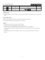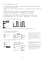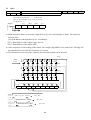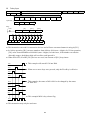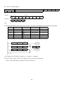
1
pLocon Ex1 Ex2 Programmable Logic Controller User’s Manual 健昇科技股份有限公司 JS AUTOMATION CORP. 台北縣汐止市中興路100號6樓 6F, No.100, Chungshin Rd. Shitsu, Taipei (221), Taiwan, R.O.C. TEL:+886-2-2647-6936 FAX:+886-2-2647-6940 http://www.automation.com.tw/ Email : [email protected] 1 CONTENTS 1. 2. 3. 4. 5. 6. 7. Specifications ........................................................................................................................................ 3 Basic Instructions................................................................................................................................ 16 Step Ladder Instructions ..................................................................................................................... 28 Advanced Devices............................................................................................................................... 32 Applied Instructions............................................................................................................................ 41 5.1. << MODBUS RTU >> CRC Error Check Mode................................................................ 91 5.2. << MODBUS ASCII >> LRC Error Check Mode ............................................................. 92 5.3. << Other Mode >> User Defined Error Check ................................................................... 93 Special Auxiliary Relay & Data Register ......................................................................................... 132 Index A........................................................................................................................................... 145 2 1. Specifications Master Unit & Expansion Unit d EXADP f g Master e Expansion I/O c h i z Master unit, Expansion I/O unit, Expansion module and EXADP communication module all can assembly to c (35mm) z Open e connector cover, connected master unit and expansion i/o unit or expansion module. z Open d connector cover, connected master unit and EXADP communication module. z f is the LED monitor of input relay, output relay, power, run status and error status. z g is the terminal of input relay, h is the terminal of output relay. z i is EEPROM card. EX - 32 M R No Mark:AC110/220V, D : DC24V Type of output: R: Relay, T: Transistor M: Master , E: Expansion I/O points (16,24,32) No Mark or 1n : can expansion, 1s: can’t expansion, Series name Dimension (mm) C 130 70 39.6 140 80 48 87 90 B 80 A 3 Performance Specification ITEM Operating control method I/O control method Operation time Programming language Program capacity / memory General Number of instruction Applied Input Relay Output Relay Auxiliary Relay (M) State Relay (S) Timer (T) Latched General Special Latched General 100 msec 10 msec 1 ms integration 100 ms integration Analog 16bits Counter 32bits Counter High Speed Counter Latched Data Register General Special Index JMP,CALL Pointer (P) Pointer ( I ) Interrupt ( I ) Nest Nest (N) Communication Interface The 2-nd port (Option) Calendar (Option) Counter (C) Constant(K) Decimal Constant(H) Hexadecimal Ex1s Ex1n Ex2n Cyclic operation by stored program Batch processing method (when END instruction is executed) Basic instruction 0.5us, Applied instruction from 2us to several 100us. Relay symbolic language + Step ladder 8000 steps ( built in EEprom ) Basic instruction:27, Step ladder instruction:2 106 108 119 Sink/Source DC24V 7mA photo coupler isolation X00~X17 X000 ~ X177 Relay : AC250V/1A or Transistor : DC30V/0.5A Y00~Y17 Y000 ~ Y177 M000 ~ M499 ( EEprom backup ) M500 ~ M1535 (no backup) M8000 ~ M8255 (no backup) S000 ~ S499 ( EEprom backup ) S500 ~ S999 (no backup) T000 ~ T199 (no backup) T200 ~ T245 (no backup) 4 points, T246 ~ T249 (EEPROM backup) 6 points, T250 ~ T255 (EEPROM backup) 2 points (Define by user) Latched C00 ~ C31 (EEprom backup) General C32 ~ C199 General C200 ~ C215 Latched C216 ~ C255 (EEprom backup) 6 points : X0 ~ X5 ; X0 or X1 for 1 phase 60KHz , X2 ~ X5 for 1phase 10KHz X0 and X1 for 2 phase 30KHz , X2 ~ X5 for 2phase 5KHz D000 ~ D255 (EEprom backup) D256 ~ D3999 (can used FNC(12) MOV stored at EEPROM) D8000 ~ D8255 (no backup) V0 ~ V7, Z0 ~ Z7 P000 ~ P127 I0xx ~ I8xx N0 ~ N7 RS-232C & RS-232C/RS-422,RS-485 Week, Year, Month, Day, Hour, Minute, Second 16 bits: -32,768 ~ +32,767 32 bits: -2,147,483,648 ~ +2,147,483,647 16 bits: 0000h ~ FFFFh 32 bits: 00000000h ~ FFFFFFFFh General Specification Item Description Source Voltage Supply current Momentary power failure Breakdown voltage Isolation resistance Noise Impedance Grounding Ambient Temperature Ambient humidity Atmosphere AC 85~264 V 50/60 Hz 24VDC / 800 mA Keep operation in 10 ms AC1500/1min (between output terminal and frame ground terminal) DC500v/5mΩ Noise voltage: 1000Vp-p, noise width: 1 us Class 3 ground 0 ~ 55°C 35 ~ 85 RH (without condensation) Must be free from corrosive gasses 4 Input Specification Item Circuit DC input (Sink) 24V Input voltage Input current Impedance Response time Input pattern Circuits isolation DC input (Source) 24V VCC 24G 24G S/S S/S X00 X00 DC24V+10%, -15% 7mA / DC24V 3.3 KΩ About 10 ms (X00~X07 High Speed) No voltage contact or NPN open collector Photo coupler VCC DC24V+10%, -15% 7mA / DC24V 3.3 KΩ About 10 ms (X00~X07 High Speed) No voltage contact or PNP open collector Photo coupler Output Specification Item Circuit Relay output Transistor output TRIGGER CIRCUIT Y0 RY CO Load voltage Rated current Rated capacity Response time Circuits isolation Under AC250V DC30V 2A / 1 point 100W About 10ms Machine isolation DC5V ~ 30V 0.5A / 1 point 12W Under 1 ms Photo coupler Note of Output Specification Ex1s Ex1n Transistor output module haven’t pulled high resistor 2.2K Ex32MT-P Transistor output module have pulled high resistor 2.2K 5 Y0 CO Source Power Wiring Diagram ( NPN Mode ) (24⊕, 24 is output power source from PLC) AC85 ∼264V 50/60Hz LX FG NX • • 24⊕ S/S 24 X0 DC/DC ….. ….. X17 5V GND Master Unit (MR type) 24⊕ 24 • • C0 Y0 Y1 DL Y2 Y3 MC ….. ….. Y17 ….. X17 load Source Power Wiring Diagram ( PNP Mode ) (24⊕, 24 is output power source from PLC) AC85 ∼264V 50/60Hz LX FG NX • • 24⊕ S/S 24 X0 DC/DC ….. 5V GND Master Unit (MR type) 24⊕ 24 • • C0 Y0 DL Y1 Y2 MC 6 Y3 ….. load ….. Y17 16MR Type Terminal Signal (24⊕ → S/S is NPN mode,24 → S/S is PNP mode) (24⊕, 24 are output power source from PLC) AC85 ∼264V 50/60Hz NX FG 24VDC LX 24⊕ 24 S/S X00 X01 X02 X03 X04 X05 X06 X07 C1 Y04 Y05 Y06 Y07 X03 X04 X05 X06 X07 C1 Y04 Y05 Y06 Y07 X03 X04 X05 X06 X07 Y02 Y03 C1 Y04 Y05 PLC 24⊕ 24 C0 Y00 Y01 Y02 Y03 16MR Type Terminal Signal (PNP mode Source) (24⊕, 24 are output power source from PLC) AC85 ∼264V 50/60Hz 24 24⊕ NX FG 24VDC LX S/S X00 X01 24⊕ 24 C0 Y00 Y01 Y02 X02 PLC Y03 14MT Type Terminal Signal and Wiring Diagram (24⊕, 24 are output power source from PLC) AC85 ∼264V 50/60Hz NX FG LX COM X00 X01 X02 24VDC PLC 24⊕ 24 24I CA0 Y00 Y01 CA1 (Internal power mode used and connected with driver) 24V *option …. 24G pulse …. *option sign …. Servo Driver 7 …. …. …. 14MT Type Terminal Signal and Wiring Diagram (24⊕, 24 are output power source from PLC) AC85 ∼264V 50/60Hz NX FG LX COM X00 X01 X02 X03 X04 X05 X06 X07 Y02 Y03 C1 Y04 Y05 24VDC PLC 24⊕ 24 24I CA0 Y00 Y01 CA1 (External power mode used and connected with driver) 24V *option 24G pulse …. …. *option sign …. …. …. …. Servo Driver 14MT Type Terminal Signal and Wiring Diagram (24⊕ → S/S is NPN mode, 24 → S/S is PNP mode) (24⊕, 24 are output power source from PLC) AC85 ∼264V 50/60Hz NX FG LX S/S X00 X01 X02 X03 X04 X05 X06 X07 Y02 Y03 C1 Y04 Y05 24VDC PLC 24⊕ 24 24I CA0 Y00 Y01 CA1 (Internal power mode used and connected with driver) 24V *option …. 24G pulse …. *option sign …. …. …. …. Servo Driver 14MT Type Terminal Signal and Wiring Diagram (24⊕ → S/S is NPN mode, 24 → S/S is PNP mode) (24⊕, 24 are output power source from PLC) AC85 ∼264V 50/60Hz NX FG LX S/S X00 X01 X02 X03 X04 X05 X06 X07 Y02 Y03 C1 Y04 Y05 24VDC PLC 24⊕ 24 24I CA0 Y00 Y01 CA1 (External power mode used and connected with driver) 24V *option 24G pulse …. …. *option sign …. Servo Driver 8 …. …. …. 24MR Type Terminal Signal (24⊕ → S/S is NPN mode, 24 → S/S is PNP mode) (24⊕, 24 are output power source from PLC) AC85 ∼264V 50/60Hz NX FG LX • • 24⊕ S/S 24 X00 X01 X02 X03 X04 X05 X06 X07 X10 X11 X12 X13 X14 X15 X16 X17 24VDC PLC 24VDC 24⊕ 24 • • C0 Y00 Y01 Y02 Y03 C1 Y04 Y05 Y06 Y07 • • • • • • • • • • 24MT Type Terminal Signal and Wiring Diagram (24⊕ → S/S is NPN mode, 24 → S/S is PNP mode) (24⊕, 24 are output power source from PLC) AC85 ∼264V 50/60Hz NX FG LX • • 24⊕ S/S 24 X00 X01 X02 X03 X04 X05 X06 X07 X10 X11 X12 X13 X14 X15 X16 X17 24VDC PLC 24VDC 24⊕ 24 24I CA0 Y00 Y01 CA1 Y02 Y03 C1 Y04 Y05 Y06 Y07 • • • • • • • • • • (Internal power mode used and connected with driver) *option *option …. …. sign …. …. …. …. …. …. …. …. …. …. …. …. …. …. …. …. 24V 24G pulse Servo Driver 24MT Type Terminal Signal and Wiring Diagram (24⊕ → S/S is NPN mode, 24 → S/S is PNP mode) (24⊕, 24 are output power source from PLC) AC85 ∼264V 50/60Hz NX FG LX • • 24⊕ S/S 24 X00 X01 X02 X03 X04 X05 X06 X07 X10 X11 X12 X13 X14 X15 X16 X17 24VDC PLC 24VDC 24⊕ 24 24I CA0 Y00 Y01 CA1 Y02 Y03 C1 Y04 Y05 Y06 Y07 • • • • • • • • • • (External power mode used and connected with driver) *option *option …. …. 24V 24G pulse sign …. …. …. …. …. …. …. …. …. …. …. …. …. …. …. …. Servo Driver 9 32MR Type Terminal Signal (24⊕ → S/S is NPN mode, 24 → S/S is PNP mode) (24⊕, 24 are output power source from PLC) AC85 ∼264V 50/60Hz NX FG LX • • 24⊕ S/S 24 X00 X01 X02 X03 X04 X05 X06 X07 X10 X11 X12 X13 X14 X15 X16 X17 24VDC PLC 24VDC 24⊕ 24 • • C0 Y00 Y01 Y02 Y03 C1 Y04 Y05 Y06 Y07 C2 Y10 Y11 Y12 Y13 C3 Y14 Y15 Y16 Y17 32MT Type Terminal Signal and Wiring Diagram (24⊕ → S/S is NPN mode, 24 → S/S is PNP mode) (24⊕, 24 are output power source from PLC) AC85 ∼264V 50/60Hz NX FG LX • • 24⊕ S/S 24 X00 X01 X02 X03 X04 X05 X06 X07 X10 X11 X12 X13 X14 X15 X16 X17 24VDC PLC 24VDC 24⊕ 24 24I CA0 Y00 Y01 CA1 Y02 Y03 C1 Y04 Y05 Y06 Y07 C2 Y10 Y11 Y12 Y13 C3 Y14 Y15 Y16 Y17 (Internal power mode used and connected with driver) *option *option …. …. sign …. …. …. …. …. …. …. …. …. …. …. …. …. …. …. …. 24V 24G pulse Servo Driver 32MT Type Terminal Signal and Wiring Diagram (24⊕ → S/S is NPN mode, 24 → S/S is PNP mode) (24⊕, 24 are output power source from PLC) AC85 ∼264V 50/60Hz NX FG LX • • 24⊕ S/S 24 X00 X01 X02 X03 X04 X05 X06 X07 X10 X11 X12 X13 X14 X15 X16 X17 24VDC PLC 24VDC 24⊕ 24 24I CA0 Y00 Y01 CA1 Y02 Y03 C1 Y04 Y05 Y06 Y07 C2 Y10 Y11 Y12 Y13 C3 Y14 Y15 Y16 Y17 (External power mode used and connected with driver) *option *option …. …. 24V 24G pulse sign …. …. …. …. …. …. …. …. …. …. …. …. …. …. …. …. Servo Driver 10 16EX Type Terminal Signal (24V → S/S is NPN mode, 24G → S/S is PNP mode) (24V, 24G are external power source input terminal) 24VDC • 24V S/S 24G X00 X01 • 24V S/S 24G X10 X11 X02 X03 X04 X05 X06 X07 X13 X14 X15 X16 X17 PLC X12 16ER, 16ET Type Terminal Signal (24V → S/S is NPN mode, 24G → S/S is PNP mode) (24V, 24G are external power source input terminal) 24VDC • 24V S/S 24G X00 X01 • • C0 Y00 Y01 Y02 X02 X03 X04 X05 X06 X07 C1 Y04 Y05 Y06 Y07 PLC Y03 16EYR, 16EYT Type Terminal Signal ( not need external power source input) C10 Y10 Y11 C11 Y12 Y13 • • C0 Y00 Y01 Y02 C12 Y14 Y15 C13 Y16 Y17 C1 Y04 Y05 Y06 Y07 PLC Y03 11 24ER, 24ET Type Terminal Signal (24V → S/S is NPN mode, 24G → S/S is PNP mode) (24V, 24G are external power source input terminal) 24VDC • • • • • 24V S/S 24G X00 X01 X02 X03 X04 X05 X06 X07 X10 X11 X12 X13 X14 X15 X16 X17 • • • • C0 Y00 Y01 Y02 Y03 PLC C1 Y04 Y05 Y06 Y07 • • • • • • • • • • 32ER, 32ET Type Terminal Signal (24V → S/S is NPN mode, 24G → S/S is PNP mode) (24V, 24G are external power source input terminal) 24VDC • • • • • 24V S/S 24G X00 X01 X02 X03 X04 X05 X06 X07 X10 X11 X12 X13 X14 X15 X16 X17 • • • • C0 Y00 Y01 Y02 Y03 PLC C1 Y04 Y05 Y06 Y07 12 C2 Y10 Y11 Y12 Y13 C3 Y14 Y15 Y16 Y17 485ADP Type Terminal Signal 8EX Type Terminal Signal (24V, 24G are external power source input terminal) (24V, 24G are external power source input terminal) 24VDC 24VDC 24V 24G X00 X01 X02 X03 24V FG PLC 24V 24G X04 • 24G • • SG SG PLC X05 X06 X07 RDA RDB SDA SDB 8ER, 8ET Type Terminal Signal 1PG Type Terminal Signal (24V → S/S are NPN mode, 24G → S/S are PNP mode) (24V, 24G are external power source input terminal) 24VDC 24V 24G X00 X01 X02 PG+ PG- S/S 24I 24G FP X00 X01 DOG X03 PLC PLC • C0 Y00 Y01 Y02 RP COM CLR Y03 24VDC 8EYR, 8EYT Type Terminal Signal LTOC Type Terminal Signal (not need external power source input) • C1 Y04 • C0 Y00 Y05 Y06 Y07 PZ Y02 Y03 Vin COM 5Vo /PZ PLC PA /PA PB /PB A B CR+ CR- RP CR PLC Y01 24VDC 232ADP Type Terminal Signal Z 5Vout CTOL Type Terminal Signal (24V, 24G are external power source input terminal) FP+ 24VDC 24V FG 24G SG TX FP- RX RP+ PLC 24V 24G 5V PLC • • • • • RP- • 24VDC 13 5Vout FP 2DA Type Terminal Signal 2AD Type Terminal Signal (24V, 24G are external power source input terminal) (24V, 24G are external power source input terminal) 24VDC 24VDC 24V FG 24G V1 I1 C1 • • • 24V FG 24G V2 I2 C2 V1 I1 C1 PLC V2 I2 C2 (24V, 24G are external power source input terminal) 24VDC 24VDC 24V FG 24G • V1 C1 V2 C2 V3 C3 V4 24V C4 FG PLC C5 V6 I6 C6 V7 • • • V2+ V2- • 24G PLC I7 C7 V8 I8 V1+ C8 8TC Type Terminal Signal V1- • 2LD Type Terminal Signal (24V, 24G are external power source input terminal) (24V, 24G are external power source input terminal) 24VDC 24VDC 24V FG 24G • V1+ V1- V2+ V2- V3+ V3- V4+ V4- 24V FG PLC V5+ V5- • 2TC Type Terminal Signal (24V, 24G are external power source input terminal) I5 • PLC 8AD Type Terminal Signal V5 • • • • 5V- L2- L2+ 24G PLC • V6+ V6- • V7+ V7- • V8+ V8- • 5V+ 4AD Type Terminal Signal L1- L1+ 2PT Type Terminal Signal (24V, 24G are external power source input terminal) (24V, 24G are external power source input terminal) 24VDC 24VDC 24V 24G V1 V3 I3 C3 C1 V2 C2 24V FG 24G I4 C4 b1 B1 A1 PLC V4 (24V, 24G are external power source input terminal) 24VDC 24G V1+ V3+ V3- • V1- V2+ V2- V4- • PLC V4+ • • b2 B2 A2 PLC 4TC Type Terminal Signal 24V • 14 Note for Wiring ♦ Don’t wire it to the mark ( • ) of terminal. ♦ Can’t use the same cable for the signal wire of input and output. ♦ Don’t put the signal cable of input and output with power cable at the same tube. ♦ The expansion module with power device, so can’t wire the 24⊕ of expansion module to the 24⊕ of master. ♦ There is no power device in expansion I/O unit, so have to connect 24⊕ of master unit to 24V or 24I of expansion I/O unit, otherwise can’t input signal. ♦ If there is no enough space, but have to arrange it to two lines, then can install wire extension module (50cm length of Ex1nNEXT-50 or 80cm length of Ex1nNEXT-80), as left picture. ♦ In principle, when system is more than 128 points, then have to install power extension module (ExPower-E), as below picture. Master Unit Min 50mm Expansion Wire ( 2.0in ) Expansion Unit Ex1nNEXT-50 or Ex1nNEXT-80 Ex1n32MR Ex1n32ER Ex1n32ER Ex1n32ER 15 ExPower-E Ex1n32ER 2. Basic Instructions List of Basic Instruction Symbol Function LD LoaD Each logic start A contact Circuit & Devices X,Y,M,S,T,C LDI LoaD Inverse Each logic start B contact X,Y,M,S,T,C AND AND Serial connection A contact X,Y,M,S,T,C ANI ANd Inverse Serial connection B contact X,Y,M,S,T,C OR OR Parallel connection A contact X,Y,M,S,T,C ORI OR Inverse Parallel connection B contact X,Y,M,S,T,C ANB ANd Block Serial connection of Parallel circuit ORB OR Block Parallel connection of serial circuit OUT OUT Final operation coil drive Y,M,S,T,C LDP LoaD rising Pulse Initial logical operation Rising edge pulse X,Y,M,S,T,C LDF LoaD Falling pulse Initial logical operation Falling edge pulse X,Y,M,S,T,C ANDP AND Pulse Serial connection of Rising edge pulse X,Y,M,S,T,C ANDF AND Falling ORP OR Pulse Serial connection of Falling edge pulse Parallel connection of Rising edge pulse X,Y,M,S,T,C ORF OR Falling Parallel connection of Falling edge pulse X,Y,M,S,T,C NOP NOP No operation PLS PULSE Rising edge pulse PLS YM PLF PLF Falling edge pulse PLF YM♣ SET SET Set a bit device Permanently ON SET YMS♣ RST ReSeT Reset a bit device Permanently OFF MC Master Control Denote the start of Master control block MC MCR Master Control Reset Denote the end of Master control block MCR INV INVerse Invert the current result of the internal PLC operations MPS PuSh Push the result of operation to stack MPS MRD ReaD Read the result of operation from stack MRD MPP PoP Pop & remove the Result from stack END END Main program end X,Y,M,S,T,C N/A RST YMSTCDVZ N YM N ↗ ↗ MPP ↗ Forced the current program scan to step 0 ♣ : Special Auxiliary Relay 16 EX Load & Load Inverse & Out Instruction Mnemonic Instruction LD LoaD LDI LoaD Inverse OUT OUT EX1S Symbol & Device EX1N EX2N Step number ( ) ( ) 1 X,Y,M,S,T,C 1 X,Y,M,S,T,C ( ) Y,M,S,T,C 1 ♦ If each logic line start an NO contact, use the LD instruction. LD OUT X0 ↙ ↙ ( Y0 ) LD X 0 OUT Y 0 ♦ If each logic line start an NC contact, use the LDI instruction. LDI OUT X1 ↙ ↙ ( Y1 ) ( T0 ) K 50 LDI X 1 OUT Y 1 OUT T 0 (SP) K 50 ♦ When use hand held programmer, the space key needs to be pressed to enable the constant to be entered. AND & AND Inverse Instruction Mnemonic EX Instruction AND AND Symbol & Device ( ) X,Y,M,S,T,C ANd Inverse ANI ( X,Y,M,S,T,C ♦ If an NO contact is connected in series, use the AND instruction. AND X2 X3↙ ( Y2 ) LD X 2 AND X 3 OUT Y 2 ♦ If an NC contact is contacted in series, use the ANI Instruction. ANI X2 X3↙ LD ( Y3 ) X0 ( Y0 ) X1 ( Y1 ) X 2 ANI X 3 OUT Y 3 LD X 0 OUT Y 0 AND X 1 OUT Y 1 17 ) EX1S EX1N EX2N Step number 1 1 EX OR & OR Inverse Instruction Mnemonic Instruction OR OR ORI OR Inverse EX1S Symbol & Device EX1N EX2N Step number ( ) ( ) 1 X,Y,M,S,T,C 1 X,Y,M,S,T,C ♦ If an NO contact is connected in parallel, use the OR instruction. LD X4 ( Y4 ) ← OR X5 X 4 OR X 5 OUT Y 4 ♦ If an NC contact is connected in parallel, use the ORI instruction. X4 ( Y4 ) ← ORI X5 LD X 4 ORI X 5 OUT Y 4 ANB Instruction EX Mnemonic Instruction ANB ANd Block EX1S Symbol & Device ( EX1N EX2N Step number ) 1 N/A ♦ Serial connection of parallel circuit, use the ANB X10 X12 ( Y10 ) X11 X13 LD X 10 OR X 11 LD X 12 OR X 13 Y 10 ANB OUT EX ORB Instruction Mnemonic Instruction ORB OR Block Symbol & Device ( ♦ Serial connection of parallel circuit, use the ORB X10 X12 LD ( Y11 ) AND X11 X13 ← ORB X 10 X 12 LD X 11 AND ORB X 13 OUT Y 11 18 EX1N EX2N Step number ) N/A EX1S 1 EX Load Pulse & Load Falling Pulse Instruction Symbol & Device EX1S EX1N EX2N Mnemonic Instruction Step number LDP LoaD rising Pulse X,Y,M,S,T,C 2 LDF LoaD Falling pulse X,Y,M,S,T,C 2 LDP X0 ↙ " M100 X1 " LDF X0 0 2 3 4 6 LDP OR OUT LDF OUT X X M X Y 0 1 100 0 0 ↙ Y0 Basic points to remember: ♦ Connect LDP and LDF instructions directly to the left hand bus bar. ♦ Or use LDP and LDF instructions to define a new block of program when use ORB and ANB instructions (see later sections). ♦ LDP is active for one program scan after the associated device switches from OFF to ON. ♦ LDF is active for one program scan after the associated device switches from ON to OFF. Single Operation flags M2800 to M3071 ♦ When the pulse operation instructions used with auxiliary relays M2800 to M3071, only activate the first instruction encountered in the program scan, after the point in the program where the device changes. Any other pulse operation instructions will remain inactive. ♦ This is useful for use in STL programs (see chapter 3) to perform single step operation using a single device. ♦ Any other instructions (LD, AND, OR, etc.) will operate as expected. 19 AND Pulse & AND Falling Pulse Instruction EX Symbol & Device EX1S EX1N Mnemonic Instruction Step number ANDP AND Pulse X,Y,M,S,T,C 2 ANDF AND Falling pulse X,Y,M,S,T,C 2 ANDP ↙ M40 T10 M100 " X1 ANDF ↙ X0 EX2N C0 " Y4 0 1 2 4 5 6 8 LD OR ANDP OUT LDF ANDF OUT M X T M X C Y 40 1 10 100 0 0 4 Basic points to remember: ♦ Use the ANDP and ANDF instructions for the serial connection of pulse contacts. ♦ Usage is the same as for AND and ANI; see earlier. ♦ ANDP is active for one program scan after the associated device switches from OFF to ON. ♦ ANDF is active for one program scan after the associated device switches from ON to OFF. Single operation flags M2800 to M3071: ♦ When used with flags M2800 to M3071, only the first instruction will activate. 20 OR Pulse & OR Falling Pulse Instruction Symbol & Device EX1N EX2N Instruction ORP OR Pulse X,Y,M,S,T,C 2 ORF OR Falling pulse X,Y,M,S,T,C 2 SET M50 " Y4 " X1 ORP Y7 EX1S Mnemonic M40 X0 EX M24 X1 0 1 3 4 5 6 7 9 10 LD ORP SET LD AND LD ORF ORB OUT M X M X M Y X 40 1 50 0 24 7 1 Y 4 ORF Basic points to remember: ♦ Use the ORP and ORF instructions for the parallel connection of pulse contacts. ♦ Usage is the same as for OR and ORI; see earlier. ♦ ORP is active for one program scan after the associated device switches from OFF to ON. ♦ ORF is active for one program scan after the associated device switches from ON to OFF. Single operation flags M2800 to M3071 ♦ When used with flags M2800 to M3071, only the first instruction will activate. 21 Step number EX NOP & END Instruction EX1S EX1N EX2N Mnemonic Instruction Symbol & Device Step number NOP NOP N/A 1 END END END 1 NOP Instruction ♦ After the program “all clear operation” is executed, all instructions in the program are over written with NOP’s. END INSTRUCTION ♦ Insert this instruction at the end of a program and program return to step 0. ♦ If missing this instruction, then program can’t be executed. NOTE : 1 : Program a circuit from its up to down and left to right. 2 : Output relay can’t be connected directly from the bus bar. If necessary, connect it through the N/C contact of special auxiliary relay M8000. 3 : I/O relay, inside auxiliary relay, TIM/OUT the number of contact that can be used per output relay is not limited. 4 : Behind the output coil can not in addition contact; Two or more output coils can be connected in parallel. 22 EX Multiplex output circuit Mnemonic Instruction Symbol & Device MPS Memory PuSh MRD Memory ReaD MPP Memory PoP ↗ ( ) ↗ ( ) ↗ ( ) MPS MRD MPP EX1S EX1N EX2N Step number 1 1 1 ♦ In pLocon EX series, there are (11) stack memory space can store operation result, so MPS instruction may be used up to (11) times continuously. ♦ MPS: Push the operation result into stack and the stack pointer increment by 1. ♦ MRD: Read the operation result from stack and the stack pointer unchanged. ♦ MPP: Pop the operation result from stack. First the stack pointer decrement by 1. ♦ MPS,MRD,MPP are all no operand. X00 ( Y00 ) X01 ( Y01 ) X02 MPS X03 ( Y02 ) X04 ↗ ↗ MPP AND X 03 OUT Y 02 X Y X 04 03 10 X Y 11 04 MPP ( Y04 ) ( Y05 ) MPS ( Y06 ) AND OUT X13 ↗ MRD 00 00 01 01 02 AND OUT LD X12 ↗ MRD X Y X Y X ( Y03 ) X10 MPP X11 MPS LD OUT AND OUT LD MPS X14 MRD ( Y07) AND X 12 OUT Y 05 AND X 13 OUT Y 06 AND X 14 OUT Y 07 MRD MPP 23 EX Master Control ( MC/MCR ) Mnemonic Instruction MC Master control MCR Master Control Reset X10 MC N0 N0 M10 M10 X1 LD MC SP Symbol & Device X N M MC N MCR EX1N EX2N Step number Y,M 2 N 1 10 0 10 LD X 1 ( Y0 ) OUT Y 0 LD X 2 ( Y1 ) MCR N0 OUT MCR Y N 1 0 X2 EX1S ♦ N is the nesting level number. ♦ The MC/MCR instructions are used in pairs when branch a circuit to plural OUT instruction. ♦ When the MC condition is ON, the state of each relay is the same as in an ordinary circuit with out MC/MCR instruction. ♦ When the MC condition is OFF, the state of each relay between the MC and MCR instruction is as following: Time, Device for OUT Counter, Device for SET Reset & OFF Hold present state ♦ Be sure that an LD/LDI instruction will be always following MC/MCR instruction. 24 EX Inverse ( INV ) Mnemonic Instruction INV INVerse X0 PLS M0 SET Y0 PLF M1 RST Y0 Symbol & Device EX1N " X1 " 0 1 3 4 5 6 8 9 LD PLS LD SET LD PLF LD RST X M M Y X M M Y EX2N Step number N/A M0 M1 EX1S 1 0 0 0 0 1 1 1 0 Basic points to remember: ♦ The INV instruction is used to change (invert) the logical state of the current ladder network at the inserted position. ♦ Usage is the same as for AND and ANI; see earlier. Usages for INV ♦ Use the invert instruction to quickly change the logic of a complex circuit. It is also useful as an inverse operation for the pulse contact instruction LDP, LDF, ANP, etc. 25 EX PLS / PLF (Pulse Output) EX1S EX2N Mnemonic Instruction PLS PuLSe PLS Y.M. 2 PLF PuLse Falling PLF Y.M. 2 X0 PLS Y0 PLF Y1 X1 Symbol & Device EX1N LD PLS X Y LD X 1 PLF Y 1 Step number 0 0 ♦ When X0 pulse OFFÆON, the specified devices of PLS is enabled “1” scan cycle. X0 Y0 ♦ When X1 pulse ONÆOFF, the specified devices of PLF is enabled “1” scan cycle. X1 Y1 ♦ The special auxiliary relay can’t be for PLS/PLF used. SET/RST EX Mnemonic Instruction SET SET SET Y,M,S RST ReSeT RST Y,M,S,D X0 SET Y0 X1 RST Y0 Symbol & Device LD SET X Y 0 0 LD X 1 RST Y 0 EX1S EX1N EX2N Step number Y.M. :1 Special M,S Coils :2 D, special D, registers, V and Z :3 X0 X1 Y0 ♦ SET : While operation result is on the specified device is enabled. Once enabled, the specified device remains enabled even if the operation result is disabled. ♦ RST : While operation result is on the specified device is reset, word device cleared to “0”. 26 TIMER & COUNTER EX Mnemonic Instruction OUT OUT RST RST Symbol & Device ( RST T.C ) EX1S EX1N EX2N Step number K.. T,C 32 bit counter : 5 Others :3 T.C : 2 << Timer >> X0 LD OUT ( T0 ) T0 K50 ( Y0 ) X T 0 0 K 50 LD T 0 OUT Y 0 ♦ When X0 on, T0 active after 5 seconds T0 contact ON, and keep current data even through X0 keep ON. X0 T0 coil 5 sec ♦ When X0 off, then clear T0 to “0” and contact off, T0 contact ♦ Timer can be set directly by using constant K or indirectly by using data register (D). Y0 ( T0 ) D0 ♦ All of the timers (T000~T255) are unlatched. << Counter >> X0 RST C0 X1 ( C0 ) C0 LD RST X C 0 0 LD X 1 OUT C 0 K5 ( Y0 ) K 5 LD C 0 OUT Y 0 X0 X1 C0 When X0 ON, clear C0 current data to“0” and contact off. ♦ C0 count up the signal of X1 (OFFÆON), after 5 counts then keep current value and the contact ON. ♦ Counters can be set directly using constant K or indirectly by using data register (D). ♦ ( C0 ) D0 ♦ All of the counters (C0 ~ C255) are latched. ♦ The high speed counters refer to chapter 4. 27 3. Step Ladder Instructions How STL Operates 3.1 The state activate & move condition A ( Y0 ) SET Y1 X0 Å move condition B ( Y2 ) ( 3-1a ) A A X0 B X0 B ( 3-1b ) ( 3-1c ) When (3-1a) state A ON, execute the program belonged to state A, i.e. Y0 ON, Y1 ON, Y2 OFF. State B OFF, the program belonged to state B not executing. ♦ When move condition X0 ON (don’t need to keep), then state B ON, i.e. state A ON and state B ON in one cycle time (3-1b) Y0,Y1,Y2 all ON. ♦ After one cycle state A auto OFF, state B still ON (3-1c) i.e. Y0 OFF, Y1 ON (SET), Y2 ON. ♦ Once the current STL state activates a second following state, the source STL state will auto reset. ♦ 3.2 Simple Flow Chart (SFC)& Ladder Chart (STL) S1 S1 ( Y0 ) ( Y0 ) X0 Åmove condition X0 Å move condition SET S2 S2 S2 S2 is move destination move destination ( 3-2a ) Simple Flow Chart -SFC ( 3-2b ) Ladder - STL ♦ ( 3-2a ) is Simple Flow Chart, ( 3-2b ) is Ladder Chart. ♦ The state (S) can be connected to Output Relay directly. ♦ To Activate an STL state, need to drive the STL coil first. In the EX-series, the SET is used to drive an STL state to make it active. ♦ The formula is used M8002 & ZRST to initial STL state, and used M8002 & SET to start STL program. ♦ The RET instruction is end of STL state, let program return to ladder sequence. 28 3.3 STL&RET Operands : S0 ∼ S999 3.3.1 : Single Flow Mode M8002 S0 M8002 ( Y 10 ) SET Y11 ( T10 ) T10 S1 SET ( Y10 ) SET Y11 K50 ( Y12 ) ( T10 ) ( T11 ) T11 S2 T10 K30 RST S0 K50 SET Y11 S1 S1 ( Y13 ) ( T12 ) T12 S0 S0 ( Y12 ) ( T11 ) T11 K20 RET K30 SET S2 RST Y11 S2 ( Y13 ) ( T12 ) T12 K20 SET S0 RET Fig 3-3-1a Simple Flow Chart - SFC LD SET STL OUT SET OUT LD SET STL OUT OUT M 8002 S 0 S 0 Y 10 Y 11 T 10 K 50 T 10 S 1 S 1 Y 12 T 11 Fig 3-3-1b. Ladder - STL LD SET STL RST OUT OUT LD SET RET K T S S Y Y T K T S 30 11 2 2 11 13 12 20 12 0 ♦ The end of STL program area need added RET instruction, let program return to original bus bar. 29 3.3.2 : Selective Branch Programming M8002 S10 ( Y10 ) ( T20 ) K50 T20 X10 S11 X11 ( Y11 ) ( T21 ) S13 T23 K30 T21 S12 ( Y12 ) ( T23 ) ( Y12 ) K20 S14 ( Y11 ) ( T22 ) ( T24 ) T24 K30 T22 S15 K20 ( Y13 ) ( T25 ) K50 T25 S10 RET Fig 3-3-2a. Simple Flow Chart - SFC ♦ This type of program construction can created many flow but only one flow can enable, i.e. X10,X11 can’t ON at the same time. M8002 S14 SET S10 ( Y11 ) ( T24 ) S10 ( Y10 ) T24 ( T20 ) T20 T20 X10 K20 SET S15 S15 K50 SET S11 SET S13 ( Y13 ) X11 ( T25 ) S11 T25 K50 SET S10 ( Y11 ) ( T21 ) T21 SET S12 S12 ( Y12 ) ( T22 ) T22 K30 SET S15 S13 ( Y12 ) ( T23 ) T23 RET K30 K20 SET S14 Fig 3-3-2b Ladder - STL 0000 0001 0002 0003 0004 0005 0006 0007 0008 0009 0010 0011 0012 0013 0014 0015 0016 0017 0018 0019 0020 0021 30 LD SET STL OUT OUT LD AND SET LD AND SET STL OUT OUT LD SET STL OUT OUT M S S Y T K T X S T X S S Y T K T S S Y T K 8002 0022 10 0023 10 0024 10 0025 20 0026 50 0027 20 0028 10 0029 11 0030 20 0031 11 0032 13 0033 11 0034 11 0035 21 0036 30 0037 21 0038 12 0039 12 0040 12 0041 22 0042 30 0043 ( 3-3-2c ) LD SET STL OUT OUT LD SET STL OUT OUT LD SET STL OUT OUT LD SET RET T S S Y T K T S S Y T K T S S Y T K T S 22 15 13 12 23 20 23 14 14 11 24 20 24 15 15 13 25 50 25 10 3.3.3 : Multiple Flows Simultaneously M8002 S20 (Y0) ( Y10 ) ( T20 ) K50 T20 S21 (Y1) ( T21 ) K30 S23 T23 T21 S22 ( Y11 ) ( T23 ) K20 (Y2) S24 ( T22 ) K30 T22 T24 S25 ( Y12 ) ( T24 ) K20 (Y3) ( Y13 ) ( T25 ) K50 T25 S20 RET Fig 3-3-3a. Simple Flow Charting ♦ This type of program construction can enable multiple flow at the same time. M8002 S22 SET S24 T22 T24 S20 S20 SET S25 S25 (Y0) ( Y10 ) ( T20 ) T20 S21 (Y3) ( Y13 ) ( T25 ) K50 T25 K50 SET S21 SET S23 (Y1) SET S20 RET ( T21 ) T21 K30 SET S22 S22 (Y2) ( T22 ) K30 S23 ( Y11 ) ( T23 ) T23 K20 SET S24 S24 ( Y12 ) ( T24 ) K20 Fig 3-3-3b. Ladder - STL 0000 0001 0002 0003 0004 0005 0006 0007 0008 0009 0010 0011 0012 0013 0014 0015 0016 0017 0018 0019 0020 0021 31 LD SET STL OUT OUT OUT LD SET SET STL OUT OUT LD SET STL OUT OUT STL OUT M S S Y Y T K T S S S Y T K T S S Y T K S Y 8002 20 20 0 10 20 50 20 21 23 21 1 21 30 21 22 22 2 22 30 23 11 0022 0023 0024 0025 0026 0027 0028 0029 0030 0031 0032 0033 0034 0035 0036 0037 0038 0039 0040 0041 0042 0043 OUT LD SET STL OUT OUT STL STL LD AND SET STL OUT OUT OUT LD SET RET T K T S S Y T K S S T T S S Y Y T K T S 23 20 23 24 24 12 24 20 22 24 22 24 25 25 3 13 25 50 25 20 4. Advanced Devices Input Relays (X) & Output Relays (Y) ♦ Input Relay (X000 – X177) octal 128 points receive external switch signal, photo coupler isolation, and connect to input terminal directly. ♦ Output Relay (Y000 – Y177) octal 128 points output the signal to drive load, relay or photo coupler isolation and connect to output terminal directly. ¾ The timing of Input (X) & Output (Y) ON STATUS can’t read ¾ X00~X07 ON STATUS can read input OFF status cannot read output fresh program Input fresh output fresh IN input fresh program The number of Input (X) & Output (Y) program ( cycle time ) ¾ Auxiliary Relay (M) ♦ General auxiliary relay (M000~M511) decimal 512 points ♦ Latch auxiliary relay (M512~ M1023) decimal 512 points ♦ Special auxiliary relay (M8000~M8255) 256 points ¾ State Relay ( Mnemonic S) ♦ State relay (S000~S999) decimal 1000 points. ♦ All of state relays (S000~S999) are latched. ♦ This type relay is for SFC used. ¾ Pointer ( Mnemonic P,I) ♦ The pointer (P00-P63) decimal 64 points ♦ The pointer (P) is for CJ, CALL branch used. ♦ The number of pointer can’t use duplicate. ♦ The pointer (I) is for interrupt used. ¾ Constant ( Mnemonic K/H) ♦ Decimal constant (K) range 16 bits: -32,768 ~ +32,767. 32 bits: -2,147,483,648 ~ +2,147,483,647 ♦ Hexadecimal constant (H) data range 16 bits: 0000 ~ FFFF. 32 bits: 00000000 ~ FFFFFFFF 32 X10~X17 X20~X27 IN X30~X37 Timer ( Mnemonic T) T000 ~ T255 ♦ All of timers belong to count up internal clock pulse (10ms,100ms). When count data reaches the setting value, the contacts activated. ♦ When the drive condition OFF, the current value reset to “0” and the contact OFF, except integration Timer. ♦ Setting value of timers can constant K or can use using data register (D) indirectly. ♦ 100ms Timer: T000 ~ T199 (200 points) setting range: 0.1 ~ 3,276.7 seconds ♦ 10ms Timer : T200 ~ T245 (46 points) setting range: 0.01 ~ 327.67 seconds ♦ 1ms integration Timer : T246 ~ T249 (4 points) setting range: 0.001 ~ 32.767 seconds ♦ 100ms integration Timer : T250 ~ T255 (6 points) setting range: 0.1 ~ 3276.7 seconds ¾ Timer contact active condition and accuracy I/O fresh ( Y10 ) 2nd cycle T0 contact ON T0 Check value ( T0 ) K10 to setting value Check value timer active X10 n cycle n+1 cycle ♦ From above diagram, if the timer contact position put before timer coil, then the bad accuracy is “+2t”. ¾ The timing of Timer detailed action ♦ The timing of unlatched timer (General) When input contact X10 ON, T200 start to count 1.23sec X10 by 100ms counting method. When count value ( T200 ) K123 T200 X10 reaches to setting value, the contact act. current ( Y10 ) Setting value value When count in the midway, input contact X10 OFF, the count current value will clear to “0”. When count reaches to input contact X10 OFF, the Y10 current value of count will clear to “0” and contact returns. ♦ The timing of latched timer (Integration) X11 t1 ( T250 ) K345 T250 X12 RST T250 When input contact X11 ON, T250 count by 100ms t1+ t2 = 34.5sec X11 ( Y11 ) t2 setting value, the contact act. Integrate Time Integrate Time counting method. When counting value reaches to Setting value current value Y11 When count in the midway, input contact X11 OFF, the unchanged current value of timer (t1) input to contact and then ON, then from current value to count up until to setting value, and contact act. Integration timer needs to use RST instruction to clear the content and the contact. X12 33 ♦ Circular Timer M8002 The program starts, enable T10 start to count, i.e. [CALL P10] not count time to check if setting value reaches. At this time, timer will become to circular timer, circulating count by 0 → 32767 → 65535 → 0 FEND M8000 ( T10 P10 K100) SRET END Counter ( Mnemonic C) C000 ~ C255 ¾ 16 bits up counter (C000~ C199, range: 1 ~ 32,767) X10 RST C00 X11 LD RST X C 10 00 X10 X11 LD X 11 ( C00 ) K5 OUT C 00 K 5 ( Y00 ) LD C 00 current OUT Y 00 C00 C00 ♦ The counter can be reset by RST at any time, value of counter is set to “0”, and contact signal is OFF. ♦ When X10 ON, clear C00 current value to “0” and contact turned OFF. ♦ When counter count the pulse (OFFÆON) number of X11, and when current value to the setting value, then the contact turned ON, and keep the current value. ♦ Counters can be set directly by using constant K or indirectly by using data register (D). ♦ Use data registers or special data registers to let content of data register become to setting value for the counter. ♦ The counter input signal ON or OFF must greater than program scan cycle time. ♦ If use other instruction to write a data which is greater than setting value to current value register, then when next count input is ON, counter output contact act and current value register will become to setting value. ♦ High Speed Counter operated by the principle of interrupt; this means they are event triggered and independent of cycle time. 34 ¾ 32 bits up/down counter (C200~ C234) range: (-2,147,483,648 ~ +2,147,483,647) X12 X12 up count up count ( M8200 ) down count X13 X13 RST C 200 X14 X14 ( C 200 ) K -5 5 4 C 200 4 3 (Y1) current value 2 3 2 1 1 0 0 -1 -1 -2 -2 -3 -3 -4 -4 -5 -5 -6 -7 -7 -6 -8 Y1 ♦ Through X14 count input to drive C200’s coil one time, the current value of counter will be increment or decrement. When the current value from ”-6” increase to “-5” or from “-4” decrease to “-5”, the output contact set to ON. If from ”-5” decrease to “-6” or from “-5” increase to “-4”, then output contact OFF ;i.e., current value = setting value ON, others are OFF. ♦ If the current value is +2,147,483,647, when increment by “1” will change to -2,147,483,648. If the current value is -2,147,483,648, when decrement by “1” will change to +2,147,483,647. This counter we called it to circular counter. ♦ The counting direction assigned by special auxiliary relay M8200 - M8234. If M8xxx ON, then belong to down counter. If M8xxx OFF, then belong to up counter. ♦ If use other instruction to write a data which is greater than setting value to current value register, then when next count input, counter will still count as usual, but output contact will not be changed. ¾ High Speed Counter (C235~ C255) (High speed counter operated by interrupt and independent cycle time) ♦♦♦ 32 bits up/down latched counter ♦♦♦ ITEM Counter number 1 phase 1 direction C235 ~ C245 1 phase bi-direction C246 ~ C250 2 phase bi-direction C251 ~ C255 Counter direction According to ON/OFF by M8235 ~M8245 to decided direction According different input point to decided up count or down count When A-phase ON, B-phase: 0Æ1: Up, 1Æ0:Down Direction monitor --- Monitor M8246 ~ M8255 status, then can know counter direction ifference of the 16 bit / 32 bit counters ♦♦♦D ITEM Direction Value range Setting method Current value Output contact reset ♦♦♦ 16 bit counter 32 bit counter Up counter Up / down counter direction can be change 0 ~ 32,767 -2,147,483,648 ~ +2,147,483,647 Constant (16 bit) or data register Constant (32 bit) or a pair of register No change to maximum value Change to maximum value (ring counter) To maximum value set and keep status Up counter: keep status, down counter: reset When RST instruction be driven, the value of counter reset to zero and output contact OFF 35 ¾ NOTE ♦ The input signal of high speed counter cannot be higher than counting speed. ♦ If an input is already being used by a high speed counter, it cannot be used for any other high speed counters or for any other purpose, like as an interrupt input. Input X0 X1 X2 X3 X4 X5 X6 X7 ♦♦♦Device Table of High Speed Counter ♦♦♦ 1 Phase without start/reset 1 Phase with start/reset 1 Phase bi-direction A-B Phase counter C235 C236 C237 C238 C239 C240 C241 C242 C243 C244 C245 C246 C247 C248 C249 C250 C251 C252 C253 C254 C255 U/D U/D R U/D U/D U/D R U/D R U/D U/D U/D U D U/D R U/D R S U D R U D R U D R A B U D R S S A B R A B R A B R A B R S S S U: up counter input, D: Down counter input, A: A-phase input, B: B-phase input, R: Reset input, S: Start input ♦ Inputs X0 ∼X7 cannot be used for more than one counter. For example: If C235 is used the following counters (C241, C244, C246, C247, C249, C251, C252, C254, I0xx & SPD) cannot be used. ♦ X6 & X7 also as high speed input point, but only as START or RESET input used, cannot as counter input. ♦♦Following is 2 Phase Encoder Forward & Reverse Pulse Conduction, Need used AB Phase Counter ♦♦ A phase A phase B phase B phase Forward Pulse, Count Up. Reverse Pulse, Count Down. 36 ¾ 1 Phase High Speed Counter (High speed counter operated by interrupt and independent cycle time) z1 Phase 1 Input without start/reset C235~C240 ( control M8xxx ON/OFF status, then can set Cxxx counting direction) X10 ♦This example used X10 control C235 counting direction, X00 is counting input. ♦When X12 ON, C235 start counting the input pulse (OFFÆON) of X00. ♦When X11 ON, reset C235 current value to ”0”, and the contact turned OFF. ( M8235 ) X11 RST C235 X12 ( C235 ) K –5 z1 Phase 1 Input with start/reset C241~C245 ( control M8xxx ON/OFF status, then can set Cxxx counting direction) ♦X10 control counting direction, X00 counting input, X01 reset input, X06 start input. ♦When X12 ON and X06 ON, C244 start counting the input pulse (OFFÆON) of X00. ♦When X11 or X01 ON, reset C244 current value to ”0”, and the contact turned OFF. ♦This line instruction can ignored, because can used X01 reset C244. ♦This example the content of (D1, D0) is the setting value. X10 ( M8244 ) X11 RST C244 X12 ( C244 ) D 0 z1 Phase 2 Input without start/reset C246 ( monitor M8xxx ON/OFF status, then can know Cxxx counting direction) ♦X00 as count up input point, X01as count down input point. ♦When X12 ON, C246 start counting the input pulse (OFFÆON) of X00 and X01. ♦When X11 ON, reset C246 current value to ”0”, and the contact turned OFF. X11 RST C246 X12 ( C246 ) D 2 z1 Phase 2 Input with start/reset C247~C250 ( monitor M8xxx ON/OFF status, then can know Cxxx counting direction) ♦X00 count up input point, X01 count down input point, X02 reset input,X06 start input. ♦When X12 and X06 ON, C249 counting the input pulse (OFFÆON) of X00 and X01. ♦When X11 or X02 ON, reset C249 current value to ”0”, and the contact turned OFF. X11 RST C249 X12 ( C249 ) K1234 z1 Phase 1 Input without start/reset (ex. up page) X10 count up count down X11 reset input X12 start input count up X0 count input C235 current value 5 4 3 2 1 0 4 3 2 1 0 0 -1 -1 -2 -2 -3 -3 -4 -4 -5 -6 -6 -7 C235 output contact -7 -8 37 -5 ♦ C235 use X000 as the interrupt pulse input point. (X12 is not pulse input point. Just as enable signal) ♦ Through X00 count input to drive C235 one time, current value of counter will be increment or decrement. When current value from ”-6” increase to “-5” or from “-4” decrease to “-5”, output contact is ON. If from ”-5” decrease to “-6” or from “-5” increase to “-4”, output contact is OFF ;i.e., current value = setting value ON, other OFF. ♦ If the current value is +2,147,483,647, when increment by “1” will change to -2,147,483,648. If the current value is -2,147,483,648, when decrement by “1” will change to +2,147,483,647. This counter we called it to circular counter. ♦ The counting direction assigned by special auxiliary relay M8235 - M8240.(i.e. X10 control counting direction) ♦ When the reset input to X11 is ON, C235 current value reset to ”0”, and contact turned OFF. 2 (A-B) Phase 2 Input High Speed Counter (This counter operated by interrupt and independent cycle time) ♦ EX-serial can use 2 point 2 phase 32 bits up/down counter at the same time. ♦ Monitor M8xxx ON/OFF status, then can know the counting direction of Cxxx. ♦ The counting direction of this type counter are decided by A phase and B phase, when the input pulse is ON of A phase, and when B phase input pulse is OFFÆON, then is up counter, when B phase ONÆOFF then is down counter. A phase input pulse ON. A phase input pulse ON. A phase A phase B phase B phase B phase OFFÆON is count up. X11 RST C251 X12 ( C251 ) K1234 B phase ONÆOFF is count down. ♦ This example use X00 as A phase input, X01 as B phase input, without start/rest. ♦ When X11 ON, reset C251 current value to ”0”, and the contact turned OFF. ♦ When X12 ON, enable the C251 start counting. ♦ Whether count up or count down, when current value = setting value, Y02 ON, other OFF. C251 ( Y02 ) X11 RST C254 X12 ( C254 ) K1234 C254 ♦ X00 as A phase input, X01 as B phase input, X02 as reset input, X06 as start input. ♦ When X11 or X02 ON, reset C254 current value to ”0”, and the contact turned OFF. ♦ When X12 ON, enable the C254 start counting. ♦ Whether count up or count down, when current value = setting value, Y04 ON, other OFF ( Y04 ) 38 Data Register (D) ¾ Latched Data Register (D000 – D255) 256 Points ¾ General Data Register (D256 – D3999) : General data register can be used as same as file register ♦ All of data register are 16 bits (the msb is sign), also can pair of any one to 32 bits data. ¾ Special Data Register (D8000 – D8255) 256 Points ♦ The special data register is used to control or monitor the programmable logic controller internal status. ♦ When the power OFFÆON, all of the data register are set to initial value. Index Register (V, Z) ♦ 16 bits operation mode V & Z all is 16 bits register. 32 bits operation mode pair of (V, Z) as 32 bits register V is upper word, Z is lower word. ♦ Sometime the use of multiple index registers V & Z is necessary in larger program or the program need handle large quantities of data. For Example : MOV D0Z,D100 Just change index Z value, then can move the content of D00~D99 to D100. ♦ Following instruction format can modified by index V,Z KnXxxZ, KnYxxZ, KnMxxZ, KnSxxZ, TxxZ, CxxZ, DxxZ ♦ Following is error instruction format KnZMxx ( index register V,Z can’t connect to Kn directly) ♦ Example MOV K10, Z ; index Z=10 ADD D0, D2, D100Z ; D0+D2 Æ D110 39 Binary Floating Data Binary floating data is a data register which use an continuous serial number, for example (D11, D10). S b31 27 E7 b30 26 E6 b29 25 E5 b28 D 11 (b15 ~ b0) 21 20 E1 E0 b24 b23 2-1 A22 b22 2-2 A21 b21 Exponent 8 bit Exponent 32 bit E0~E7 = 0 or 1 Exponent sign (0 : positive,1 : negative) A 0~A22 = 0 or 1 b 0~b31 = 0, then 0 when 7 0 D10 (b15 ~ b0) 2-21 2-22 2-23 A2 A1 A0 b2 b1 b0 2-3 A20 b20 -1 -2 -23 6 0 (E7×2 +E6×2 +……+E0×2 ) Binary Floating data = ± (2 +A22×2 +A21×2 +……+A0×2 ) ×2 /2127 (Example) A22=1 , A21=0 , A20=1 , A19~A0=0 E7=1 , E6~E1=0 , E0=1 7 0 -1 -2 -3 -23 Binary floating data = ± (2 +1×2 +0×2 +1×2 +……+0×2 ) ×2 = ±1.625×2129/2127=±1.625×22 positive and negative sign is decided by b31, can’t use negation. 6 0 (1×2 +0×2 +……+1×2 ) /2127 ♦ The using of zero flag(M8020), negative flag(M8021), carry flag(M8022), the flag action of floating operation as follows, Zero flag : when result is 0, then it is 1. Negative flag : when result not reach minimum unit, when it is not 0, then it is 1. Carry flag : when result more than absolute value using range, then it is 1. 40 5. Applied Instructions Applied instructions allow the user to perform complex data manipulations, mathematical operations. Each applied instruction has unique mnemonics and special function numbers. Each applied instruction will be expressed using a table similar to that show below. And will be found at the beginning of the description of each new instruction. COMPARE FNC(10) 16 bits:CMP & CMP(P) - - - - - - - - - - - - - - - - - - - 7 Steps D CMP Operands: P EX EX1S EX1N EX2N 32 bits:(D)CMP&(D)CMP(P) - - - - - - - - - - - - -13 Steps K.H. KnX KnY [ D. ] X Y M Operands: [ S1. ][ S2. ] KnM KnS T C D V,Z S No modification of the instruction mnemonic is required for 16 bit operation, and it will operate continuously, i.e. on every scan cycle of the user program, the instruction will operation and provide a new result. However, pulse operation requires a ‘P’ to be added directly after the mnemonic, while 32 bit operation requires a “D” to be added before the mnemonic. This means that if an instruction was being used with both pulse and 32 bit applied operation it would look like D***P, where *** was the basic mnemonic. The ‘pulse’ function allows the associated instruction to be Activated on the rising edge of the control input. The Instruction is driven ON for the duration of one program Scan cycle. Thereafter, even if the control input remains on the associated instruction will not be active. # Following is Symbols list: [D.]: Destination device [S.]: Source device [m,n]: Number of active devices, bits or an operational constant. # Following is instruction modifications: *** - An instruction operation in 16 bit mode, where *** identifies the instruction mnemonic. *** P- An instruction modified to use 16 bits pulse operation. D*** - An instruction modified to use 32 bits operation. 41 Condition Jump FNC(00) CJ 16 bits: CJ & CJ(P) - - - - - - - - - - - - - - - - - - - - - - 3 Steps EX EX1S EX1N EX2N P Operand: P00 ~ P63 X0 CJ P0 X1 ( Y0 ) X2 P0 ( Y1 ) Example (A) X0 X10 CJ P10 CJ X1 X11 ( Y1 ) ( Y11 ) X2 P10 X12 ( Y2 ) CJ X3 P60 X13 ( Y3 ) ( Y12 ) X4 P10 P60 X14 ( Y4 ) P60 Example (B) ( Y13 ) Example (C) ♦ Example (A): If X0 ON forces the program to jump to LAB P0, any program area which is skipped will not update. Output statuses will not change even input the devices. ♦ Example (A): If miss LAB P0 pointer, then X0 ON will jump directly to END. ♦ If a backwards jump is used, then need to care the watchdog timer overrun. ♦ If LAB pointer is duplicated to use, only the last pointer is effective. ♦ Example (B): X0 ON forces the program to jump to the second LAB pointer. ♦ Example (C): Many CJ statements can be assigned to jump to the same pointer. 42 Subroutine Call FNC(01) 16 bits: CALL & CALL(P) - - - - - - - - - - - - - - - - - - 3 Steps EX EX1S EX1N EX2N EX EX1S EX1N EX2N CALL Operand: P00~P63 P Subroutine Return FNC(02) 16 bits: SRET - - - - - - - - - - - - - - - - - - - - - - - - - - 1 Steps SRET Operand: None X0 CALL Main Program FEND X2 P0 ( Y1 ) Sub Routine SRET END P0 ♦ When X0 ON, program will jump to subroutine pointer LAB P0 and execute Subroutine until SRET instruction is executed, then program return to original step and continue processing. ♦ The LAB assigns beginning of subroutine must be programmed after an FEND. ♦ The same LAB can only be used once, but many CALL statements can be assigned to a single LAB subroutine. ♦ Subroutines can be nested for 5 levels including one CALL instruction. 43 Interrupt Return FNC(03) 16 bits: IRET - - - - - - - - - - - - - - - - - - - - - - - - - - 1 Steps EX EX1S EX1N EX2N 16 bits: EI - - - - - - - - - - - - - - - - - - - - - - - - - - - - - 1 Steps EX EX1S EX1N EX2N EX EX1S EX1N EX2N IRET Operand: None Enable Interrupt FNC(04) EI Operand: None Disable Interrupt FNC(05) 16 bits: DI - - - - - - - - - - - - - - - - - - - - - - - - - - - - - 1 Steps DI Operand: None Disable Interrupt EI Enable Interrupt DI Disable Interrupt FEND X1 I 101 ( Y1 ) Interrupt Routine IRET END ♦The programmable controller has a default status of disabling interrupt operation. ♦As under normal operation, when an interrupt routine is when an interrupt routine is activate all other interrupt are disabled. ♦Interrupt routine are always programmed after a FEND instruction. ♦ The IRET instruction may only be used within interrupt routines. Number of Interrupt pointer I 0 Interrupt Input Relay 6 points 0 : Falling Trigger, 1 : rising Trigger. No. of Input Relay X0 ∼ X5 (0 ∼ 5) (Can’t duplicate) I Timer interrupt 3points 10 ∼ 99 ms 6 , 7 , 8 (Can’t duplicate) << Note >> ♦ When an interrupt program execute, other Interrupt Call is ineffective. ♦ If Interrupt occur within the range of Disable Interrupt (DI~EI), this interrupt request signal is stored temporarily, and execute until within the range of Enable Interrupt (EI~DI). ♦ When Disable Interrupt flag M805∆ act, the corresponding Interrupt input will not be executed. 44 First End FNC(06) 16 bits: FEND - - - - - - - - - - - - - - - - - - - - - - - - - - 1 Steps EX EX1S EX1N EX2N FEND Operand: None Main Program X0 CJ Main Program FEND X1 P10 ( Y1 ) Main Program FEND X2 P20 ( Y2 ) Sub. Program SRET P10 ♦ A FEND instruction indicates the first end of a main program and the start of the subroutine program area to be used. ♦ Multiple FEND instruction can be use to separate different subroutines. ♦ When FEND is executed, the program return to Step 0. ♦ FEND can’t be used after an END instruction. END Watch Dog Timer FNC(07) 16 bits: WDT - - - - - - - - - - - - - - - - - - - - - - - - - - 1 Steps EX EX1S EX1N P WDT Operand: None X00 WDT ♦ This instruction will compare the cycle time with the content of special data register D8000. ♦ If the watch dog timer > the content of D8000, then error occurred and error code is 6309. ♦ Can use MOV instruction to change content of special data register D8000. ♦ If do not write WDT instruction in program, then the watch dog timer is ineffective. 45 EX2N FOR FNC(08) 16 bits: FOR - - - - - - - - - - - - - - - - - - - - - - - - - - - 7 Steps EX EX1S EX1N EX2N EX EX1S EX1N EX2N FOR [ S. ] Operands: K.H. KnX KnY KnM KnS T C D V,Z NEXT FNC(09) 16 bits: NEXT - - - - - - - - - - - - - - - - - - - - - - - - - - - 7 Steps NEXT Operand: None FOR K4 FOR D02 NEXT c NEXT d A B 46 ♦ After program B execute 4 times, then execute the program below d NEXT. ♦If the content of D0Z is 5, then program B is executed 4 times, and program A will be executed 20 times. ♦ The maximum nest level of FOR –NEXT is 5 levels. Compare FNC(10) D CMP 16 bits: CMP & CMP(P) - - - - - - - - - - - - - - - - - - - 7 Steps EX EX1S EX1N EX2N 32 bits: (D)CMP&(D)CMP(P) - - - - - - - - - - - -13 Steps P [ S1. ][ S2. ] Operands: K.H. KnX KnY KnM KnS T C D V,Z [ D. ] Operands: X Y M S Flag: M8020, M8021, M8022 X0 [ S1. ] K100 CMP [ S2. ] T10 [ D. ] M10 M10 K100>T10, then M10 ON M11 K100=T10, then M11 ON M12 K100<T10, then M12 ON ♦ Data of [S1.] is compared with data of [S2.] and [D.] will be changed according to the result. This will automatic occupy 3 bit destination devices from head address of designation M10 ~ M12. ♦ Full algebraic comparisons are used, i.e. -10 smaller than +2. ♦ When X0 OFF, then [D.] bit devices status will not be changed. Zone Compare FNC(11) 16 bits: ZCP & ZCP(P) - - - - - - - - - - - - - - - - - - - - 9 Steps D ZCP EX EX1S EX1N EX2N 32 bits: (D)ZCP&(D)ZCP(P) - - - - - - - - - - - - -17 Steps P [ S1. ] [ S2. ][ S3. ] Operands: K.H. KnX KnY KnM KnS T C D V,Z [ D. ] Operands: X Y M S Flag: M8020, M8021, M8022 X0 ZCP [ S1. ] K100 [ S2. ] K120 [ S3. ] T10 [ D. ] M10 M10 T10<K100, then M10 ON M11 K100≦T10≦K200, then M11 ON M12 T10>K200, then M12 ON ♦ Content of [S3.] is compared with data range of [S1.] and [S2.] and [D.] will be changed according to the result. This will automatic occupy 3 bit destination devices from head address of designation M10 ~ M12. ♦ Full algebraic comparisons are used, i.e. -10 smaller than +2. ♦ When X0 OFF, then [D.] bit devices status will not be changed. 47 Move FNC(12) D MOV 16 bits: MOV & MOV(P) - - - - - - - - - - - - - - - - - - - 5 Steps EX EX1S EX1N EX2N 32 bits: (D)MOV&(D)MOV(P) - - - - - - - - - - - - -9 Steps P [ S. ] Operands: K.H. KnX KnY KnM KnS T C D V,Z [ D. ] X0 [S.] D0 MOV [D.] K4Y0 ♦ When X0 ON, contents of source device [S.] copied to destination device [D.]. MSB D0 0 1 0 1 0 1 0 1 LSB 0 1 0 1 0 È Y17 0 1 1 0 1 È 0 1 0 1 0 1 0 1 0 1 0 Y0 1 0 1 ♦When M8027 ON, CPU will write content of [S.] into EEPROM, [D.] only D register can be used. ( M8027 ) MOV D1000 D1000 M8000 ( M8027 ) Note: When M8027 ON, for avoid to damage EEPROM, must be used Pulse Instruction MOV(P). Shift Move FNC(13) SMOV 16 bits: SMOV & SMOV(P) - - - - - - - - - - - - - - - - - 7 Steps EX EX1S EX1N EX2N EX EX1S EX1N EX2N P [ S. ] Operands: K.H. KnX KnY KnM KnS ♦Reserved T [ D. ] C D V,Z Complement FNC(14) D CML 16 bits: CML & CML(P) - - - - - - - - - - - - - - - - - - - 5 Steps 32 bits: (D)CML & (D)CML(P) - - - - - - - -- - - -9 Steps P [ S. ] Operands: K.H. KnX KnY KnM KnS T C [ D. ] X0 CML [S.] D0 [D.] K4Y0 48 D V,Z ♦ Each data bit within the source device [S.] is inverted and then copied to the designated destination [D.]. MSB D0 0 1 LSB 0 1 0 1 0 1 0 1 0 1 0 1 1 0 1 0 1 0 1 0 1 0 1 0 È Y17 1 0 0 1 1 0 È Y0 Block Move FNC(15) 16 bits: BMOV & BMOV(P) - - - - - - - - - - - - - - - - - 7 Steps BMOV EX EX1S EX1N EX2N P [ S. ] Operands: K.H. KnX KnY KnM KnS T n C D V,Z D10 [ D. ] Flag: X0 RST M8160 BMOV D10 X0 D20 [S.] D10 BMOV D19 D18 D17 D16 È È È È D29 D28 D27 D26 K10 [D.] D20 [n.] K10 D15 D14 D13 D12 D11 È È È È È D25 D24 D23 D22 D21 È D20 Ex1s, Ex1n V1.16 Edition additional function: [S.] and [D.] only D register is effective. X0 D24 Upper SET M8160 BMOV D10 D20 K4 D14 Lower D13 Upper D13 Lower D12 Upper D12 Lower D11Upper D11 Lower D10 Upper D10 Lower D24 Lower D23 Upper D23 Lower D22 Upper D22 Lower D21 Upper D21 Lower D20 Upper D20 Lower Ex1s, Ex1n V1.40 Edition additional function: [S.] and [D.] only D register is effective. When M8027 ON, CPU will write the content of [S.] into EEPROM, [D.] only D register can be used. SET M8027 [ BMOVP D10 D1000 K8] RST M8027 Note: When M8027 ON, for avoid to damage EEPROM, must be used Pulse Instruction MOV(P). 49 0 Fill Move FNC(16) 16 bits: FMOV & FMOV(P) - - - - - - - - - - - - - - - - - 7 Steps FMOV EX EX1S EX1N EX2N EX EX1S EX1N EX2N P [ S. ] Operands: K.H. KnX KnY KnM KnS T n C D V,Z [ D. ] X0 [S.] K0 FMOV [D.] D0 n K10 K0 Æ (D00 ~D09) Exchange FNC(17) 16 bits: XCH & XCH(P) - - - - - - - - - - - - - - - - - - - 5 Steps D XCH 32 bits: (D)XCH & (D)XCH(P) - - - - - - - - - - - -9 Steps P [ D1. ] Operands: K.H. KnX KnY KnM KnS T C D V,Z [ D2. ] X0 [D1.] D10 XCH [D2.] D20 Before : (D10)=100 After : (D10)=200 (D20)=200 (D20)=100 << Function of Expanded >> SWAP X0 (M8160) D XCH P M8001 D10 D10 (M8160) ♦ If M8160 ON, [D1.] and [D2.] are the same word device, then the upper 8 bits and the lower 8bits will exchange. ♦ If [D1.] and [D2.] are not the same device, error flag M8067 ON, error code 6705. Error step number is stored to D8069 and not be executed. D10 16 bits: Upper 8 bits Lower 8 bits Before executing (D10)=0050H=80,After executing (D10)=5000H=20480 32 bits: D11 D10 Upper 8 bits Lower 8 bits Upper 8 bits Lower 8 bits Before executing (D11,D10)=87654321H=80,After executing 65872143H 50 BCD (BINARY CODE TO DECIMAL) FNC(18) D BCD 16 bits: BCD & BCD(P) - - - - - - - - - - - - - - - - - - - 5 Steps P EX EX1S EX1N EX2N 32 bits: (D)BCD & (D)BCD(P) - - - - - - - - - - - -9 Steps [ S. ] Operands: K.H. KnX KnY KnM KnS T C D V,Z [ D. ] X0 [S.] D10 BCD [D.] K2Y0 ♦ The binary source data [S.] is converted into an equivalent BCD number and stored to the destination device [D.]. ♦ If the converted BCD number exceeds the operational ranges of 0 to 9999 (16 bit operation) or 0 to 99999999 (32 bit operation), an error will occur. Error flag M8067 ON, error code 6705 and error step number stored to D8069. Program will be executed continuously, but result will not be stored to [D.] ♦ This instruction can be used to output data to a seven segment display directly. BIN (DECIMAL CODE TO BINARY) FNC(19) D BIN 16 bits: BIN & BIN(P) - - - - - - - - - - - - - - - - - - - - - 5 Steps P EX EX1S EX1N EX2N 32 bits: (D)BIN & (D)BIN(P) - - - - - - - - - - - - - -9 Steps [ S. ] Operands: K.H. KnX KnY KnM KnS T C D V,Z [ D. ] X0 BIN [S.] D10 [D.] K2Y0 ♦ The BCD source data [S.] is converted into an equivalent binary number and stored at the destination device [D.]. ♦ If the source data is not provided in a BCD format, an error will occur. Error flag M8067 ON, error code 6705 and error step number stored to D8069. ♦ The device [S.] can’t be used constant K/H. 51 Addition 16 bits: ADD & ADD(P) - - - - - - - - - - - - - - - - - 7 Steps 32 bits: (D)ADD &(D)ADD(P) - - - - - - - - - -- - - 13 Steps FNC(20) D ADD P EX EX1S EX1N EX2N [ S1. ][ S2. ] Operands: K.H. KnX KnY KnM KnS T C D V,Z [ D. ] Flag: M8020, M8021, M8022 X0 [S1.] D10 ADD [S2.] D12 [D.] D14 (D10) + (D12) Æ (D14) ♦ The data contained within the source devices [S1.], [S2.] is added and the result stored to specified destination devices [D.]. ♦ All calculations are algebraically processed, i.e. 5+(-8) = -3. ♦ If the result of a calculation is “0”, then zero flag M8020 ON. ♦ If the result exceeds 32,767 (16 bit limit) or 3,147,483,647 (32 bit operation), the carry flag M8022 ON. ♦ If the result exceeds -32,767 (16 bit limit) or -2,147,483,647 (32 bit limit), the borrow flag M8021 ON. Subtraction FNC(21) D SUB P 16 bits: SUB & SUB(P) - - - - - - - - - - - - - - - - - - 7 Steps 32 bits: (D)SUB &(D)SUB(P) - - - - - - - - - - - - - 13 Steps EX EX1S EX1N EX2N [ S1. ][ S2. ] Operands: K.H. KnX KnY KnM KnS T C D V,Z [ D. ] Flag: M8020, M8021, M8022 X0 [S1.] D10 SUB [S2.] D12 [D.] D14 (D10) - (D12) Æ (D14) ♦ Content of [S1.] subtract content of [S2.], and the result stored to specified destination devices [D.]. ♦ All calculations are algebraically processed, i.e. 5 - 8 = -3. ♦ The MSB of devices is sign (0:Positive, 1:Negative). Zero Flag -2, -1, 0 –32,768 Zero Flag -1 , 0, 1 Zero Flag 32,767 , 0 , 1 , 2 Borrow Flag Carry Flag Zero Flag -2 , -1 , 0 –2,147,483,648 Borrow Flag Zero Flag -1 , 0, 1 2,147,483,647 , 0 , 1 , 2 Zero Flag Carry Flag 52 Multiplication 16 bits: MUL & MUL(P) - - - - - - - - - - - - - - - - - 7 Steps 32 bits: (D)MUL &(D)MUL(P) - - - - - - - - - - - - 13 Steps FNC(22) D MUL P EX EX1S EX1N EX2N [ S1. ][ S2. ] Operands: K.H. KnX KnY KnM KnS T C D V,Z [ D. ] X0 [S1.] D10 MUL [S2.] D12 [D.] D14 16 bit: (D10) ± (D12) Æ (D15, D14) X0 [S1.] D10 DMUL [S2.] D12 [D.] D14 32 bit: (D11,D10) ± (D13,D12) Æ (D17,D16,D15,D14) ♦ The primary source [S1.] is multiplied by the secondary source [S2.]. The result is stored to destination [D.]. Division 16 bits: DIV & DIV(P) - - - - - - - - - - - - - - - - - -- 7 Steps 32 bits: (D)DIV & (D)DIV(P) - - - - - - - - -- - - - -13 Steps FNC(23) D DIV P EX EX1S EX1N EX2N [ S1. ][ S2. ] Operands: K.H. KnX KnY KnM KnS T C D V,Z [ D. ] X0 [S2.] D12 [D.] D14 (D10) ÷ (D12) Æ (D14) . . . . . (D15) 16 bits 16 bits 16 bits 16 bits X0 [S1.] [S2.] DDIV D10 D12 [D.] D14 DIV Dividend Dividend divisor quotient divisor [S1.] D10 remainder quotient remainder (D11,D10) ÷ (D13,D12) Æ (D15,D14)…….(D17,D16) 32 bits 32 bits 32 bits 32 bits ♦ The primary source [S1.] is divided by the secondary source [S2.]. The result is stored to destination [D.]. ♦ If value of source device [S2.] is “0” (zero), then an operation error is executed. Error code 6706 and error step number stored to D8069, the program operation is cancelled. ♦ V1.17 edition:If value of source device [S2.] is “0” (zero), then will not execute and directly jump to next instruction. 53 Increment FNC(24) D INC P K.H. 16 bits: INC & INC(P) - - - - - - - - - - - - - - - - - - 3 Steps 32 bits: (D)INC & (D)INC(P) - - - - - - - - - - - - - -5 Steps KnX KnY KnM KnS Operands: T C D EX EX1S EX1N EX2N V,Z [ D. ] X0 [D.] D0 INC (D0) + 1 Î (D0) ♦ On every execution of the instruction, the device specified as the destination [D.] and its current value increased 1. ♦ In 16 bit operation, when +32,767 is reached, the next execution will write a value of -32,768 to destination device. ♦ In 32 bit operation, when +2,147,483,647 is reached, the next execution will write -2,147,483,648 to destination device. ♦ The carry, zero and borrow flag are unaffected in the operation. Decrement FNC(25) D DEC P K.H. 16 bits: DEC & DEC(P) - - - - - - - - - - - - - - - - - - 3 Steps 32 bits: (D)DEC & (D)DEC(P) - - - - - - - - -- - - - -5 Steps KnX KnY Operands: KnM KnS T C D EX EX1S EX1N EX2N V,Z [ D. ] X0 DEC [D.] D0 (D0) - 1 Î (D0) ♦ On every execution of the instruction, the device specified as the destination [D.] and its current value decreased 1. ♦ In 16 bit operation, when -32,768 is reached, the next execution will write a value of +32,767 to destination device. ♦ In 32 bit operation, when -2,147,483,648 is reached, the next execution will write +2,147,483,647 to destination device. ♦ The carry, zero and borrow flag are unaffected in the operation. 54 Logical AND FNC(26) D WAND P 16 bits: WAND & WAND(P) - - - - - - - - - - - - - - 7 Steps 32 bits: (D)WAND &(D)WAND(P) - - - - - - - - - 13 Steps EX EX1S EX1N EX2N 16 bits: WOR & WOR(P) - - - - - - - - - - - - - - - - 7 Steps 32 bits: (D)WOR & (D)WOR(P) - - - - - - - - - - -13 Steps EX EX1S EX1N EX2N 16 bits: WXOR & WXOR(P) - - - - - - - - - - - - - - 7 Steps 32 bits: (D)WXOR &(D)WXOR(P) - - - - - - - - - 13 Steps EX EX1S EX1N EX2N Logical OR FNC(27) D WOR P Logical XOR FNC(28) D WXOR P [ S1. ][ S2. ] Operands: K.H. KnX KnY KnM KnS T C [ D. ] X0 [S1.] [S2.] [D.] WAND D10 D12 D14 (D10) Λ (D12) Î (D14), 1Λ1=1, 1Λ 0=0, 0Λ1=0, X0 [S1.] [S2.] [D.] WOR D10 D12 D14 (D10) V (D12) Î (D14), 1V1=1, 1V 0=1, 0V1=1, X0 WXOR [S1.] D10 [S2.] D12 [D.] D14 (D10) V (D12) Î(D14),1V1=0,1V 0=1,0V1=1,0V 0=0. 55 D V,Z Negation 16 bits: NEG & NEG(P) - - - - - - - - - - - - - - - - - - 3 Steps 32 bits: (D)NEG & (D)NEG(P) - - - - - - - - - - - -- -5 Steps FNC(29) D NEG P K.H. KnX KnY KnM KnS T Operands: C D EX EX1S EX1N EX2N V,Z [ D. ] X0 [D.] D10 NEG /(D10)+1¼(D10) ♦ When X0 ON, the selected device [D.] is inverted. ( “1”J”0”,“0”J”1”) ♦ When this is complete, a further binary 1 is added to the bit pattern. The result is become a negative number or a negative number will become a positive. < Example >> Absolute Value of Negative M8000 BON D10 M0 K15 M0 NEG P D10 << Note of Negation >> (D 10)=2 0 0 0 0 0 0 0 (D 10)=1 0 0 0 0 0 0 0 (D 10)=0 0 0 0 0 0 0 0 (D 10)= -1 1 1 1 1 (D 10)= -2 1 1 1 1 0 0 0 0 0 0 0 1 0 0 0 0 0 0 0 0 0 1 0 0 0 0 0 0 0 0 0 1 1 1 1 1 1 1 1 1 1 1 1 1 1 1 1 1 1 1 1 1 1 0 0 0 0 0 0 0 0 0 1 0 0 0 0 0 0 0 0 0 1 0 0 0 0 0 0 0 0 0 0 0 0 0 0 0 0 0 0 0 0 (D 10)= -32,765 1 0 0 0 0 (D 10)= -32,766 1 0 0 0 0 (D 10)= -32,767 1 0 0 0 0 (D 10)= -32,768 1 0 0 0 0 (D 10)+1=1 1 → 0 0 0 0 (D 10)+1=2 0 → 0 0 0 0 0 0 0 0 0 0 0 0 0 0 0 1 0 0 0 0 0 0 0 0 0 0 1 0 1 1 1 1 1 1 1 1 0 1 1 1 1 1 1 1 1 1 1 0 1 1 1 1 1 1 1 1 1 1 0 0 0 0 0 0 0 0 0 0 (D 10)+1= 32,765 1 → 0 1 1 1 1 1 (D 10)+1= 32,766 0 → 0 1 1 1 1 1 (D 10)+1= 32,767 1 → 0 1 1 1 1 1 (D 10)+1= -32,768 0 → 1 0 0 0 0 0 56 Rotation Right 16 bits: ROR & ROR(P) - - - - - - - - - - - - - - - - - - 5 Steps 32 bits: (D)ROR & (D)ROR(P) - - - - - - - - - - - -- -9 Steps FNC(30) D ROR P K.H. KnX n Operands: Flag: M8022 X0 ROR P KnY KnM T C D 1 1 EX1N EX2N EX1S EX1N EX2N V,Z [D.] D0 [n.] K4 D0 1 EX1S [D.] MSB 1 KnS EX 1 1 1 1 LSB 0 0 0 0 0 0 0 0 M8022 È MSB 0 0 0 0 È After 1 rotation 1 1 1 1 1 1 1 1 LSB 0 0 0 0 M8022=0 ♦ After rotation right, the LSB of specified devices is shifted into carry flag M8022. Rotation Left 16 bits: ROL & ROL(P) - - - - - - - - - - - - - - - - - - 5 Steps 32 bits: (D)ROL & (D)ROL(P) - - - - - - - - - - - - - -9 Steps FNC(31) D ROL P K.H. Operands: Flag: X0 KnX KnY KnM n T C D V,Z [D.] [D.] D0 ROL P [n.] K4 MSB 1 KnS D0 1 1 EX 1 1 1 1 1 LSB 0 0 0 0 0 0 0 0 M8022 È MSB 1 1 1 1 È After 1 rotation 0 0 0 0 0 0 0 0 LSB 1 1 1 1 M8022=1 ♦ After rotation left, the MSB of specified devices is shifted into carry flag M8022. 57 Rotation Right with Carry 16 bits: RCR & RCR(P) - - - - - - - - - - - - - - - - - - -5 Steps 32 bits: (D)RCR & (D)RCR(P) - - - - - - - - - - - - - -9 Steps FNC(32) D RCR P K.H. Operands: Flag: X0 KnX KnY KnM n T C D [D.] D0 EX2N EX EX1S EX1N EX2N V,Z D0 1 EX1N [n.] K4 MSB 1 EX1S [D.] RCR P 1 KnS EX 1 1 1 1 1 LSB 0 0 0 0 0 0 0 0 M8022 When M8022 = 1, after one rotation then M8022 = 0 MSB 0 0 0 1 1 1 1 1 1 LSB 1 1 1 0 0 0 0 Rotation Left with Carry FNC(33) D RCL P K.H. Operands: Flag: X0 16 bits: RCL & RCL(P) - - - - - - - - - - - - - - - - - - - 5 32 bits: (D)RCL & (D)RCL(P) - - - - - - - - - - - - - - -9 KnX KnY KnM T C D V,Z [D.] [D.] D0 RCL P [n.] K4 MSB 1 KnS n D0 1 1 1 1 1 1 1 LSB 0 0 0 0 0 0 0 0 M8022 When M8022 = 0, after one rotation then M8022 = 1 MSB 1 1 1 1 0 0 0 0 0 LSB 0 0 0 58 0 1 1 1 Shift Right FNC(34) SFTR 16 bits: SFTR & SFTR(P) - - - - - - - - - - - - - - - - - 9 steps EX EX1S EX1N EX2N 16 bits: SFTL & SFTL(P) - - - - - - - - - - - - - - - - - 9 steps EX EX1S EX1N EX2N P Shift Left FNC(35) SFTL P Operands: [S.] K.H. n X Y M n2 =< n1 =< 255 Flag: X10 [D.] [S.] X0 SFTR P S [D.] M0 n1 K16 n2 K1 X0 È << BIT SHIFT RIGHT >> 15 14 13 12 11 X10 SFTL P 10 M9 M8 [S.] X0 M7 M6 [D.] M0 M5 M4 n1 K16 M3 M2 M1 M0 n2 K1 X0 È << BIT SHIFT LEFT >> 15 14 13 12 11 10 M9 M8 M7 M6 M5 M4 M3 M2 M1 M0 Example I/O Test: Wiring X10 Y10 … X17 Y17 M8002 SET M8013 X10 Y17 T10 X11 SFTRP X12 X13 X10 X14 Y10 X15 K8 X16 K1 X17 T10 T10 59 K5 Word Shift Right FNC(36) WSFR 16 bits: WSFR & WSFR(P) - - - - - - - - - - - - - - - - 9 steps EX EX1S EX1N EX2N 16 bits: WSFL & WSFL(P) - - - - - - - - - - - - - - - - 9 steps EX EX1S EX1N EX2N P Word Shift Left FNC(37) WSFL P [ S. ] Operands: K.H. KnX KnY KnM KnS n Flag: X10 WSFR P T C D V,Z D11 D10 [ D. ] [S.] D0 [D.] D10 n1 K10 n2 K1 D0 È D19 << WORD SHIFT RIGHT >> D18 D17 D16 D15 X10 WSFL P [S.] D0 n2 =< n1 =< 255 D14 D13 D12 [D.] D10 n1 K10 n2 K1 D0 D19 << WORD SHIFT LEFT >> n2 =< n1 =< 255 D18 D17 D16 D15 D14 D13 D12 60 D11 È D10 Shift Register Write 16 bits: SFWR & SFWR(P) - - - - - - - - - - - - - - - - 7 Steps FNC(38) SFWR EX EX1S EX1N EX2N P [ S. ] Operands: K.H. KnX KnY KnM KnS T n C D [ D. ] Flag: X10 SFWR P [S.] D0 D10 D8 [D.] D1 Source n K10 n = 10 points D0 V,Z D9 D7 D6 D5 pointer D4 D3 O D2 N D1 M ♦ When X10 OFF Æ ON, content of D0 stored into D2 and D1=”1”. When next rising pulse, content of D0 stored into D3 and D1=”2”, the position of insertion into the stack is automatically calculated by controller. ♦ If content of [D.] exceeds the value “n-1” (n is length of the FIFO stack), then insertion into the FIFO stack is stopped. The carry flag M8022 is turned ON. ♦ Before starting to use a FIFO stack, ensure that contents of the head address register [D.] are equal to “0”. Shift Register Read 16 bits: SFRD &SFRD(P) - - - - - - - - - - - - - - - - - 7 Steps FNC(39) SFRD EX EX1S EX1N EX2N P [ S. ] Operands: K.H. KnX KnY KnM KnS n T C D V,Z [ D. ] Flag: X10 [S.] D1 SFRD P [D.] D20 n K10 pointer D10 D9 D8 D7 D6 D5 D4 D3 D2 D1 D20 ♦ When X10 OFF Æ ON, content of D2 stored into D20 and content of D1 decreased 1 (D1=D1-1). ♦ When contents of source device [S.] are equal to “0”, i.e. the FIFO stack is empty, zero flag M8020 is turned on. ♦ This instruction will always read the source data from the register [S.]+1. 61 Zone Reset 16 bits: ZRST(P) - - - - - - - - - - - - - - - - - - - - - - - 5 steps FNC(40) ZRST EX EX1S EX1N EX2N P [D1.][D2.] Operands: K.H. KnX KnY KnM KnS T C D V,Z [D1.] [D2.] Operands: X Y M Flag: X0 S ZRST [D1.] S0 ZRST C235 [D2.] S99 C255 ♦ The range of specified devices are reset, for data devices, the current value is set to “0”, and for bit elements, the bit status are turned OFF. ♦ The specified device range cannot contain mixed devices types, i.e. if C00 specified as the first destination devices [D1.], then cannot paired with T99 as the second devices. ♦ If [D1.] is bigger than (>) [D2.], then only [D1.] is reset. Decode 16 bits: DECO(P) - - - - - - - - - - - - - - - - - - - - - - - 7 steps FNC(41) DECO P [ S. ] Operands: X Y M S K.H T C [ D. ] [ D. ] n=1–8 X10 [S.] X000 DECO X002 X001 X000 0 4 1 2 1 1 [D.] M10 [n.] K3 0 0 0 0 1 0 0 0 M17 M16 M15 M14 M13 M12 M11 M10 ♦ If the specified device [D.] is T, C or D, then n ≤ 4. ♦ If the sources all are “0”, then M10 set to “1”. 62 D V,Z EX EX1S EX1N EX2N Encode 16 bits: ENCO(P) - - - - - - - - - - - - - - - - - - - - - - - 7 steps FNC(42) ENCO EX EX1S EX1N EX2N P [ S. ] Operands: X Y M S K.H T C [ D. ] D V,Z [ D. ] n=1–8 Flag: X10 [S.] M10 ENCO M17 M16 M15 [D.] D10 M14 [n.] K3 M13 M12 M11 0 0 0 0 1 0 0 0 7 6 5 4 3 2 1 0 0 0 0 0 0 0 0 0 MSB 0 0 0 0 0 0 1 D10 M10 1 LSB ♦ If the specified device [S.] is T, C or D, then n ≤ 4. ♦ The number of active (ON) bits within the source device [S.] is more than one, only the highest bit effective. ♦ If bits of source device [S.] all are “0”, then error occurred. Sum FNC(43) D SUM P 16 bits: SUM(P) - - - - - - - - - - - - - - - - - - - - - - - - 5 steps 32 bits: (D)SUM(P) - - - - - - - - - - - - - - - - - - - - - -9 steps EX EX1S EX1N EX2N [ S. ] Operands: K.H. KnX KnY KnM KnS T C D V,Z [ D. ] Flag: X00 [S.] D0 SUM 0 0 1 0 0 0 1 0 0 0 1 0 [D.] D2 0 1 D 0 0 0 D 2 0 1 0 1 0 1 1 1 0 0 0 0 8 1 4 0 2 0 1 1 ♦ The number of active (ON) bits within the source device [S.], i.e. bits which have a value of “1” are counted. The count is stored in the destination device [D.]. ♦ If there is no bit as 0, then zero flag M8020 ON. 63 Bit On Check 16 bits: BON(P) - - - - - - - - - - - - - - - - - - - - - - - - 7 steps 32 bits: (D)BON(P) - - - - - - - - - - - - - - - - - - - - - 13 steps FNC(44) D BON P K.H. EX1N EX2N KnX X Flag: X10 0 KnM [S.] D10 BON 1 KnY KnS T C D EX EX1S EX1N EX2N V,Z [ n. ] = 0~15 or 0~31 [ D. ] Y M S Operands: 1 0 1 [D.] M0 0 1 [n.] K15 0 1 0 1 0 1 0 Bit15,D10=0, then M0 = OFF. 1 EX1S [ S. ] Operands: 0 EX 0 1 0 1 0 1 0 1 0 1 LSB 1 0 1 0 Bit15,D10=1, then M0 = ON 1 0 LSB Mean 16 bits: MEAN(P) - - - - - - - - - - - - - - - - - - - - - -- 7 steps FNC(45) MEAN P [ S. ] Operands: K.H. Operands: KnX KnY KnM KnS n T C [D.] [n]=1-64 Flag: X10 MEAN [S.] D0 [D.] D10 [n.] K3 ♦ [ (D0) + (D1) + (D2) ] / 3 Æ (D10) 64 D V,Z Annunciator Set FNC(46) 16 bits: ANS - - - - - - - - - - - - - - - - - - - - - - - - - - 7 steps EX EX1S EX1N EX2N 16 bits: ANR(P) - - - - - - - - - - - - - - - - - - - - - - - - 1 steps EX EX1S EX1N EX2N 16 bits: SQR(P) - - - - - - - - - - - - - - - - - - - - - - - - 5 steps EX EX1S EX1N EX2N ANS Reserved Annunciator Reset FNC(47) ANR Reserved Square Root FNC(48) D SQR P 32 bits: (D)SQR(P) - - - - - - - - - - - - - - - - - - - - - -9 steps Flag: M8020, M8021, M8022 X000 [S.] [D.] SQR D10 D12 D10→D12 ♦ [S.] must be positive. When it is negative, error flag M8067 ON, and stop executing. ♦ When the result with decimal fraction, don’t care it; but borrow flag M8021 will ON. ♦ When result is 0, zero flag M8020 will ON. 65 Float 16 bits: FLT(P) - - - - - - - - - - - - - - - - - - - - - - - - - 5 steps FNC(49) EX EX1S EX1N EX2N D FLT P 32 bits: (D)FLT(P) - - - - - - - - - - - - - - - - - - - - - - -9 steps Flag: M8020, M8021, M8022 ♦ FLT Instruction is converted command between BIN integer and binary floating data. Because constant K, H will automatically convert when floating data operate, then not fit this instruction X000 [S.] D10 FLT [D.] D12 ( D10 ) → BIN integer ( D13、D12 ) binary floating data X000 M8023 FLT D10 D12 M8000 ( D11、D10 ) → binary floating data ( D12 ) BIN integer Decimal fraction don’t care M8023 X000 D FLT D10 D12 ( D11、D10 ) → BIN integer ( D13、D12 ) binary floating data X000 M8023 D FLT D10 M8000 D12 ( D11、D10 ) binary floating data M8023 → ( D13、D12 ) BIN integer Decimal fraction don’t care ♦ When M8023 = ON, execute binary floating data → BIN integer。 When M8023 = OFF, then execute BIN integer → binary floating data. ♦ Binary floating data → BIN integer, the operating result is decimal fraction, don’t care it, but M8021 / M8022 will ON; when result is 0, M8020 will ON 66 Output & Input Refresh 16 bits: REF(P) - - - - - - - - - - - - - - - - - - - - - - - - 5 steps FNC(50) REF EX EX1S EX1N EX2N P Operand: [D.] should always be a multiple of 10, i.e. 00,10.. [n.] should always be a multiple of 8, i.e. 8,16,24.. ♦ PLC input all refresh before program STEP 0 execute; output is executed after END or FEND instruction. It is not changed in performing process. If it needs immediately input data or output performing result in the performing process, then have to use output & input refresh instruction. << Input Fresh >> only X10 – X17 to be flashed X00 [D.] [n.] REF X10 K8 << Output Fresh >> refresh Y00-Y07, Y10-Y17, Y20-Y27. X01 [D.] [n.] REF Y00 K24 Refresh and Filter Adjustment 16 bits: REFF(P) - - - - - - - - - - - - - - - - - - - - - - - 3 steps FNC(51) REFF EX EX1S EX1N EX2N P Operand: [n.] = 0 - 60 X10 REFF K20 ♦ To avoid noise interference, PLC input relay all designed with hardware RC filter to adjust software filter time. ♦ This instruction only change X00-X07 software filter time, i.e., content of D8020. If it has to change other input point filter time, please use MOV instruction. 67 Matrix FNC(52) 16 bits: MTR - - - - - - - - - - - - - - - - - - - - - - - - - - - 9 Steps EX EX1S EX1N EX2N MTR Operand: (S.): X00, X10, X20, X30 - - - - - - - X160, X170. (D1.): Y00, Y10, Y20, Y30 - - - - - - Y160, Y170. (D2.): Y, M, S multiple of 10, i.e. 00, 10, 20 etc. (n.): K, H. n=2 ~ 8. M8000 [S.] [D1.] [D2.] [n.] MTR X10 Y10 M20 K3 M8029 ♦ MTR instruction allows 8 consecutive input devices [S.] to be used multiple (n) times. The result was stored in (D2.). (S.): Head address of the input devices. (n.): row numbers. (D1.): Head address of the output trigger devices. (D2.): Head address of the matrix table. ♦ After completion of full reading of the matrix, the complete flag M8029 to be turned ON. This flag will be automatically reset when this instruction is executed. ♦ This instruction can be used once, and only the transistor module can be selected. M47 M46 M45 M44 M43 M42 M40 DIODE 0.1A50V M41 ROW3 M37 M36 M35 M34 M33 M32 M31 M30 ROW2 COMX M27 M26 M25 M24 M23 M22 M20 M21 ROW1 X10 X11 X12 X13 X14 X15 X16 X17 Y10 Y11 Y12 Y13 Y14 Y15 Y16 Y17 PLC COMY M8000 ROW1 X10 ∼ X17 Y10 STATUS ROW2 X10 ∼ X17 Y11 STATUS M30 ∼ M37 d ROW3 X10 ∼ X17 Y12 M20 ∼ M27 c STATUS M40 ∼ M47 O 68 Set by High Speed Counter FNC(53) EX D HSCS EX1S EX1N EX2N 32 bits: HSCS - - - - - - - - - - - - - - - - - - - - - - - - 13 Steps [ S1. ] Operands: K.H. KnX KnY KnM KnS T C D V,Z [ S2. ] : C235~C255 Operands: X Y M S [D.] When [D.], can use Index to assign I010~I060 to interrupt. Flag: M8000 C253 K2, 147, 483, 647 [S1.] [S2.] [D.] D HSCS K100 C253 Y000 D HSCR K200 C253 Y000 ♦ When use FNC53, operate external output action by interrupt. When current value of C253 changed from 99 to 100 and from 101 to 100, Y000 will be set. When current value of C253 is changed from 199 to 200 and from 201 to 200, Y000 OFF. ♦ This command is specialized instruction of 32 bits, please input D HSCS command. ♦ Only can use FNC53, FNC54, FNC55 once. M8000 C253 K2, 147, 483, 647 [S1.] [S2.] D HSCS K100 C253 [D.] I010 ♦ Therefore, when current value of High Speed Counter which is FEND I010 ♦[D.] of D HSCS can assign I0 □ 0 = (□=1~6)(□=1~6 can not be reuse.) Interrupt program assigned by [S2.] is as same as the value which is assigned by [S1.], interrupt main program and jump to execute I0 □ 0 interrupt program immediately. IRET END ♦When Special auxiliary relay M8059 ON, I010~I060 interrupt are all prohibited. 69 Reset by High Speed Counter FNC(54) EX D HSCR EX1S EX1N EX2N 32 bits: HSCR - - - - - - - - - - - - - - - - - - - - - - - - 13 Steps [ S1. ] Operands: K.H. KnX KnY KnM KnS T C D V,Z [ S2. ] : C235~C255 Operands: X Y M S [D.] Can assign [D.] and [S2.] are the same High Speed Counter. Flag: M8000 C253 K300 D HSCR K400 C253 ♦ When current value of C253 is 400, C253 will be cleared immediately. Current value will become 0, and output contact will not act. C253 400 300 Current value of C253 C253 output contact ♦ This command is specialized instruction of 32 bits, so have to use D HSCR. Zone Compare For High Speed Counter FNC(55) EX D HSZ EX1S EX1N EX2N 32 bits: HSZ- - - - - - - - - - - - - - - - - - - - - - - - - - 17 Steps [ S1. ] Operands: K.H. KnX KnY KnM KnS T C D V,Z [ S2. ] : C235~C255 Operands: X Y M S [D.] Flag: M8000 C251 D HSZ K2, 147, 483, 647 [S1.] [S2.] K1000 K2000 <Compare action of input> K1000>C251 current value K1000≦C251 current value≦K2000 K2000<C251 current value [S.] [D.] C251 Y000 Y000 Y001 Y002 ON ON ON ♦ This command is specialized instruction of 32 bits, so have to use D HSZ. ♦ Content of [S1.] and [S2.] is according to [S1.] ≦ [S2.] . ♦ When use FNC55, operate external output by Interrupt. Output will act without effect by scan-cycle. 70 Speed Detect FNC(56) 16 bits: SPD - - - - - - - - - - - - - - - - - - - - - - - - - - - 7 Steps EX EX1S EX1N EX2N SPD Operands: (S1.): X000~X005. When C251 is used, X02 and X03 can not be used. [ S2. ] Operands: K.H. KnX KnY KnM KnS T C D V,Z Flag: M8029 [D.] SPD [S1.] X00 [S2.] K100 [D.] D00 ♦ The input pulse assigned by [S1.], and the [S2.] assign measurement time, the result will be stored at [D.]. ♦ This will automatic occupy 3 word devices from the head address of [D.]. (D00~D02) ♦ This example D01 count up the pulse number of X00 (OFFÆON), and put the result into D00 at 100msec after. Then reset D01to “0” and start counting again. ♦ D02 is used to measurement remainder time. ♦ The counting pulse amount of the assign time can’t be more than 65535 ♦ Following formula can calculated RPM RPM : N = (D00¯60) ¯ 1000 / n ¯ t n: (pulse/revolution), t: (measurement time). ♦ The pulse frequency of (X00-X05) is same with HSC. ♦ If input relay (X00-X05) is assigned by the SPD, they can’t be used to other purpose or interrupt input point. ♦ If pulse output assign Y00, then X00 can’t be used; if assign Y01, then X01 can’t be used. ♦ V1.45 or more, add complete flag M8029, easily reach many data of continuous measurement, then count an average value. 71 ( i ) measure frequency mode X10 X00 D01 : current value D00 : measurement value 100ms 100ms 100 D02 : remainder time ( ii ) measure cycle mode Time base (1ms) X10 X00 D0:measurement value (ms) D1:current value ♦ When the content of [S2.] is ”0”, then it’s measurement cycle mode. ♦ The measurement time (ms) and RPM are inverse ratio, it can get number of turning round by formula thereinafter RPM = N = 60 × 1000/D0 72 Pulse Output FNC(57) 16 bits: PLSY(P) - - - - - - - - - - - - - - - - - - - - - - - - 7 steps D PLSY EX EX1S EX1N EX2N 32 bits: (D)PLSY(P) - - - - - - - - - - - - - - - -- - - 13 steps [ S1. ][ S2. ] Operands: K.H. KnX KnY KnM KnS T C D V,Z [D.] : Y00 – Y01 Flag: M8029 X10 [S1.] K1000 PLSY [S2.] D00 [D.] Y00 number of pulse ( D0 ) Y000 1KHz ♦ This instruction is pulse output without slope. ♦ [S1.] : assign output frequency (1~5000Hz), [S2.]: assign output pulse [D.]: assign pulse output point ♦ PLSY is used to output a consecutive pulse 16 bit range: 1 ~ 32,767, 32 bit range: 1 ~ 2,147,483,647. ♦ If [S2.] is specified to 0, then it will continue to generate pulse. ♦ The pulse duty cycle is 50% ON 50% OFF. ♦ Data of [S2.] can be changed during execution, but the new will not be effective until current operation has been completed, and complete flag M8029 set to ON . ♦ This instruction can be used once, and only the transistor module can be selected. Pulse Width Modulation FNC(58) 16 bits: PWM - - - - - - - - - - - - - - - - - - - - - - - - - - 7 steps EX PWM [ S1. ][ S2. ] Operands: K.H. KnX KnY KnM KnS T C D V,Z [D.] : Y00 – Y03 Flag: None X10 [S1.] PWM D10 [S2.] K50 [D.] Y00 t Y000 T0 ♦ [S1.]: ON duty width (t), range: (1 ~ 32,767 msec) ♦ [S2.]: (T), range: (1 – 32,767 msec) ♦ [D.]: The output point (Y). (by interrupt handing) ♦ If content of [S1.] is bigger than content of [S2.], then error occurred. ♦ This instruction can be used once, and only the transistor module can be selected. 73 EX1S EX1N EX2N PULSE OUTPUT WITH SLOPE FNC(59) 16 bits: PLSR - - - - - - - - - - - - - - - - - - - - - - - - - - - 9 steps D PLSR EX EX1S EX1N EX2N 32 bits: (D)PLSR- - - - - - - - - - - - - - - - - - - - - 17 steps [ S1. ][ S2. ][S3.] Operands: K.H. KnX KnY [D.] : Y00 – Y01 Flag: M8029 X10 [S1.] PLSR K1000 KnM [S2.] D00 KnS [S3.] K1000 T C D V,Z [D.] Y00 ♦ [S1.] assign output frequency.(10 ~ 100,000 pps), [S2.] assign opposite position (M8134,M8135=0) or absolute position (M8134,M8135=1)output pulse. [S3.] assign acceleration/deceleration time. When set acceleration/deceleration separate flag is just for acceleration time, then D8165 and D8167 are deceleration time. [D.] assign pulse output point. (Fix Y00 and Y01 to be pulse output point, and Y02, Y03 to be direction output point). ♦ When use this instruction, have to convert increment distance or absolute position to pulse, then stored at [S2.]. ♦ The pulse duty cycle is 50% ON, 50% OFF ♦When pulse output, X10 OFF, pulse is stopped outputting immediately. ♦When instruction running, changing content of [S2.] is ineffective. ♦This instruction for Y00 or Y01 only can be used once (total twice), and have to select transistor output type. ♦ There is only one kind of pulse output type in this instruction (Negative Logic Type, Pulse & Sign) can be controlled step or servo motor. pulse sign ♦(X00: Y00 0 signal, X01:Y01 0 signal, X06:Y00 dog point signal, X07:Y01dog point signal) X00 Zero1 X01 Zero2 X02 X03 X04 X05 X06 Dog1 X07 Dog2 ♦Use this instruction for zero return, dog point must assigned to X06(Y00) or X07(Y01), and servo zero must assigned to X00(Y00) or X01(Y01). Servo End & Servo Ready are assigned by user. ♦This is a multifunction, so PLSR can execute JOG, zero return, single position drive by setting different flag. ♦When zero return, if there is no zero signal (stepping motor), set parameter D8169 or D8171 to ”0”. ♦Fixed Y00 and Y01 to Pulse output signal; Y02 and Y03 to Sign output signal. ♦ After this instruction execute, acceleration and deceleration time D8164 and D8166 data will be changed to [S3.] 74 ¾ FNC(59) Zero Return EX(1) ( This Example Initial Direction controlled by Flag M8156 or M8157 ) Initial Direction also can be controlled by the absolute address of dog point M8002 MOV K100 D8168 Setting Y00 Bias Speed Frequency ( 1 word ) MOV K100 D8164 Setting Y00 Accelerate Time and Decelerate Time (ms) (1 word) DMOV K100,000 D8156 Setting Y00 Maximum Speed Frequency ( 2 words ) DMOV K500 D8176 Setting Y00 Dog Point Absolute Address ( 2 words ) ZRST M100 M199 DMOV K50,000 D116 Setting Home Speed Frequency DMOV K1000 D118 Setting Creep Speed Frequency MOVP K5 D8169 SET M112 RST M8152 Clear zero return finish flag RST M8158 Initial direction decided by M8156 SET M8156 Initial direction reverse SET M8154 Forward Mode ( if M8154=0 then is reverse mode ) SET X12 M8144 Setting FNC(59)PLSR zero return mode, FNC(156)ZRN Don’t Care This M8002 Setting the number of search z phase X12 M112 Home D116 DPLSR M8029 M8152 RST RST Don’t Care D118 M112 M8029 75 Acc. Dec. Creep Speed = D8168 Dog point is X06 pulse catch flag M8176 effective K100 Y00 ¾ FNC(59)Zero Return EX(2) (Initial direction controlled by dog point absolute position) Also could choose Initial direction to be controlled by flag M8156 or M8157 If bias absolute position greater than dog point absolute position, then reverse. If bias absolute position less than dog point position, then forward. M8002 MOV K100 D8170 Set Y01 bias speed frequency MOV K100 D8166 Set Y01 acceleration, deceleration time (ms) DMOV K100,000 D8158 Set Y00 maximum speed frequency DMOV K500 D8178 Set Y00 dog point absolute position ZRST M100 M199 DMOV K50,000 D126 Set Home Speed DMOV K1000 D128 Set MOVP K5 D8171 Set search number of Z phase SET M113 RST M8153 clear zero return finish flag SET M8159 Initial direction control by (D8179,D8178) SET M8157 M8159=1, This Flag Don’t Care RST M8155 Reverse mode ( if M8155=1, then forward mode ) SET X13 M8144 M8002 X13 M113 Set FNC(59)PLSR zero return mode, FNC(156)ZRN Don’t Care This Home D126 DZRN M8029 M8153 RST RST Don’t Care acceleration, deceleration time Creep Speed = D8170 D128 K100 Y00 Dog point fixed X07 pulse catch flag M8177 effective M113 M8029 76 ¾ Example FNC(59) Jog+ and Jog- (M8029 ineffective) X14 X16 ( M8146 ) Y00 Jog+ Flag X15 X17 ( M8147 ) Y01 Jog+ Flag X16 X14 ( M8148 ) Y00 Jog- Flag X17 X15 M8146 M8198 ( M8149 ) Y01 Jog- Flag M8148 M8196 M8147 M8199 M8149 M8197 DPLSR D110 D112 K100 Y00 DPLSR D120 D122 K100 Y01 ¾ Example first position drive M8002 MOV K100 D8168 Set Y00 axis bias speed frequency MOV K100 D8164 Set Y00 axis Acc/Deceleration time(ms) MOV K1000 D8165 Set Y00 axis Deceleration time(ms) DMOV K100,000 D8156 Set Y00 axis maximum speed frequency SET M8150 SET M110 Set Y00 axis Acc/Deceleration time separate flag X10 M110 X10 DPLSR M8029 D110 D112 RST M110 RST M8029 77 K100 Y0 Initial State FNC(60) 16 bits: IST - - - - - - - - - - - - - - - - - - - - - - - - - - - - 7 steps EX EX1S EX1N EX2N 16 bits: SER(P)- - - - - - - - - - - - - - - - - - - - - - - - -9 steps EX EX1S EX1N EX2N IST Reserved Data Search FNC(61) D SER P 32 bits: (D)SER(P) - - - - - - - - - - - - - - - - - - - 17 steps Reserved 78 Absolute Drum Sequence FNC(62) 16 bits: ABSD - - - - - - - - - - - - - - - - - - - - - - - - - - 9 steps EX EX1S EX1N EX2N ABSD X000 [S1.] ABSD C0 [S2.] D300 C0 RST C0 [D.] M0 n This instruction is used to bring a varied output type to counter. It can detect the angle of the circle control action. K4 X001 ♦Left example is used to control ON/OFF status of Auxiliary Relay M0~M3 when rotation table rotate within a circle. X001 C0 K360 Rotation angle signal (1angle/pulse) ♦ Using MOVE instruction to write following values into D300~D307 ON setting value D300= 40 D302= 100 D304= 160 D306= 240 OFF setting value D301= 140 D303= 200 D305= 60 D307= 280 Output point M0 M1 M2 M3 Put Turn ON value to even number of D device, and put Turn OFF value to Odd number of D device ♦When X0 ON, change of M0~M3 is mentioned as follows. Turn ON and Turn OFF value can re-change to write into D300~D307 40 140 ♦Output point number is decided by setting value of [D.] ♦When X0 become OFF, output is not changed. M0 100 200 M1 60 160 M2 240 280 M3 0 180 360 ♦ABSD instruction just can be used once in one program. ♦When assign High Speed Counter in [S.], then also can use (D)ABSD instruction. For current value of counter at this time, the output status will delay because of scan-time, recommend to use Table high-speed compare mode of HSZ instruction. 79 Incremental Drum Sequence FNC(63) 16 bits: INCD - - - - - - - - - - - - - - - - - - - - - - - - - - 9 steps EX EX1S EX1N EX2N INCD X000 [S1.] INCD [S2.] D 300 C0 [D.] M0 n This instruction is used to produce a varied output when using a couple of counter. K4 M8013 C0 K9999 1sec pulse signal Following is the control range of 4 points (M0~M3) ♦Use MOVE instruction to write following value into [S1.] in advance. D300 = 20 D301 = 30 D302 = 10 D303 = 40 X000 40 C0 current value 20 C1 Current value M0 M1 M2 M3 M8029 complete flag 30 10 20 ♦When counting value of C0 reach to setting value of D300~D303, C0 reset automatically in turn ♦C1 count occurred number of C0 reset. ♦M0~M3 act in turn according to counting value of C1. ♦After complete last operation of setting number by ”n”, flag M8029 become ON. Above mentioned action will be always repeated. ♦ When X0 OFF, C0 and C1 is cleared, M0~M3 become OFF, then operate again when X0 become ON. ♦INCD instruction only can be used once in one program. Teaching Timer FNC(64) 16 bits: TTMR - - - - - - - - - - - - - - - - - - - - - - - - - - 5 steps EX EX1S EX1N EX2N 16 bits: STMR - - - - - - - - - - - - - - - - - - -- - - - - - - 7 steps EX EX1S EX1N EX2N TTMR Reserved Special Timer FNC(65) STMR Reserved 80 Alternate Output FNC(66) 16 bits: ALT(P) - - - - - - - - - - - - - - - - - - -- - - - - - - 3 steps ALT EX EX1S EX1N EX2N EX EX1S EX1N EX2N P [ D. ] Operands: X Y M Flag: X00 S [D.] M00 ALTP X00 M00 Ramp FNC(67) 16 bits: RAMP - - - - - - - - - - - - - - - - - - -- - - - - - - 9 steps RAMP Operands: [ S1. ][ S2. ][D.] : D n: Flag: M8029 X00 RAMP K,H [S1.] D1 n = 1 to 32,767 [S2.] D2 [D.] D3 n K1000 ♦ When X0 ON, content of [S1.] and [S2.] are stored into [D.]. Content of [D.] is increased by “1” each scan cycle. n: the number of scan cycle. (D2) (D1) (D3) (D2) (D1) (D3) n scan cycle time Scan cycle time stored at D4 n scan cycle time D1 < D2 D1 > D2 ♦ After M8029 is driven, write once scan-time value (longer than actual scan-time) into M8039, and then PLC will enter to fixed scan mode. For example, n = K1000 in above example. If scan cycle is set to 20msec, then value in D3 will be changed from setting value of D1 to setting value of D2 within 20sec. ♦ If X0 become OFF when acting, then act of RAMP signal will stop in midway. If X0 ON again, then D4 will be cleared and D3 will restart by setting value of D1. ♦ After end of execution, flag M8029 act, and then value of D3 will return to value of D1. ♦ Control of start / end point can be executed by RAMP instruction and analog output. ♦ Enter into RUN status when X0 ON. 81 Rotary Control FNC(68) 16 bits: ROTC - - - - - - - - - - - - - - - - - - -- - - - - - - 9 steps EX EX1S EX1N EX2N 16 bits: SORT - - - - - - - - - - - - - - - - - - -- - - - - - 11 steps EX EX1S EX1N EX2N ROTC Reserved Sort FNC(69) SORT Reserved 82 Tenkey Input 16 bits: TKY - - - - - - - - - - - - - - - - - - - - - - - - - 7 Steps 32 bits: (D)TKY - - - - - - - - - - - - - - - - - - - - - -- 13 Steps FNC(70) D TKY Operands: EX EX1S EX1N EX2N [D1.] K.H. KnX KnY KnM M S KnS T C D V,Z [ S. ] Operands: X Y [D2.] Flag: X20 TKY [S.] X000 [D1.] D00 [D2.] M10 COM X00 X01 X02 X03 X04 X05 X06 X07 X10 X11 PLC ♦ This instruction can read 10 consecutive devices and will store an entered numeric string in [D1]. ♦ In 16 bits operation, [D1] can store numbers from 0000 to 9999 (max. 4 digits). In 32 bits operation, [D1] value from 00000000 to 99999999 (max. 8 digits). In both cases, if the number exceeds the allowable ranges, the highest digit will overflow, and ignored it. ♦ When X20 OFF, all of the [D2.] devices are reset, but contents of [D1.] keep intact. f X00 d X01 X02 X03 M10 ♦ This example will stored 2130 into D00. ♦ When two or more keys were pressed, only the First Key is effective. c e ♦ This example, the status of M10~M19 to be changed by the status of X00~X11. M11 M12 M13 ♦ This example M20 is key release flag. M20 ♦ This instruction may only be used once. 83 Hexadecimal Key 16 bits: HKY - - - - - - - - - - - - - - - - - - - - - - - - - 9 Steps 32 bits: (D)HKY - - - - - - - - - - - - - - - - - - - - - - 17 Steps FNC(71) D HKY EX EX1S EX1N EX2N [ D2. ] Operands: K.H. KnX KnY KnM KnS T C D V,Z [D3.] Operands: X Y M [D1.] [S.] Flag: X14 S [S.] X10 HKY [D1.] Y10 C D E F 8 9 A B 4 5 6 7 0 1 2 3 [D2.] D0 [D3.] M0 COMX X10 X11 X12 X13 X14 X15 X16 X17 COMY Y10 Y11 Y12 Y13 Y14 Y15 Y16 Y17 ♦ When the numeric key (0 ~ 9) be pressed, then causes bit device [D3.]+7 turn ON for the duration of key press. ♦ When the function key (A ~ F) be pressed, then causes bit device [D3.]+6 turn ON for the duration of key press. ♦ When the function key has been pressed, then will set bit devices [D3.]+0 to [D3.]+5 to ON, and remain ON until the next function key has been activated. F E D C B A M5 M4 M3 M2 M1 M0 ♦ In 16 bits operation, [D2.] can store numbers from 0000 to 9999 (max. 4 digits). In 32 bits operation, [D2.] value from 00000000 to 99999999 (max. 8 digits). In both cases, if the number exceeds the allowable ranges, the highest digit will overflow, and ignored it. ♦ When two or more keys were pressed, only the first key is effective. When X14 OFF, all [D3.] devices are reset, but contents of [D2.] keep intact. ♦ This instruction requires 8 scans cycle time to read the key input. After 8 scans, complete flag M8029 to be turned ON. This flag is automatically reset when this instruction execute. ♦ This may only be used once, and only the transistor module can be selected. 84 Digital Switch 16 bits: DSW - - - - - - - - - - - - - - - - - - - - - - - - - 9 Steps FNC(72) EX EX1S EX1N EX2N DSW Operands: Operands: [n] K.H. =1~8 KnX KnY KnM [S.] X [D1.] Y M S Flag:M8029 X00 DSW [S.] X10 KnS [D1.] Y10 0 [D2.] D0 1 10 2 C 3 10 4 8 COM X10 X11 X12 X13 V,Z [n] K4 2 10 1 T [D2.] D 10 1 2 4 8 X14 X15 X16 X17 COM Y10 Y11 Y12 Y13 0 10 1 2 3 10 10 10 ♦ This instruction used n (1~8) output points and 4 input points to read in n (1~8) thumbwheel switch. If the read data is larger than 32 bits (n≥5), then [D2.] automatically occupy the next word device. ♦ This example the BCD 4 digit thumbwheel switch (1,2,4,8) is connected to X10~X13 or X14~X17, the source [S.] needs to be used X10,X14,X20,X24….as the head address. ♦ Once DSW execute, then the flag M8029 reset to “0”. When execution is completed, M8029 set to ”1”. ♦ Each pin (1,2,4,8) of the thumbwheel switch needs to be connected a diode (0.1A/50V) ♦ This may only be used once, and only the transistor module can be selected. If use M8029, then can control two or more DSW . M8002 SET M500 M500 DSW X10 Y10 D0 K2 D2 K6 M8029 RST M500 SET M501 M501 DSW X10 Y12 M8029 RST M501 SET M500 85 Seven Segment Decoder 16 bits: SEGD(P) - - - - - - - - - - - - - - - - - - - - - - - 5 steps FNC(73) SEGD EX EX1S EX1N EX2N P [ S. ] Operands: K.H. KnX KnY KnM KnS T C D V,Z [ D. ] Flag: X00 SEGD [S.] D00 [D.] K2Y0 ♦ A single hexadecimal digit (0~9, A~F) occupying the lower 4 bits of the source device [S.] is decoded to a data format used to drive a seven segment display. ♦ The decoded data is stored in the lower 8 bits of destination device [D.]. The upper 8 bits was unchanged. ( S. ) ( D. ) Seven segment display Hex Bit 0 1 2 3 4 5 6 7 8 9 A B C D E F 0000 0001 0010 0011 0100 0101 0110 0111 1000 1001 1010 1011 1100 1101 1110 1111 b0 b5 b6 b4 b3 b1 b2 data b7 b6 b5 b4 b3 b2 b1 b0 0 0 0 0 0 0 0 0 0 0 0 0 0 0 0 0 0 0 1 1 1 1 1 0 1 1 1 1 0 1 1 1 0 0 0 1 1 1 1 1 1 1 1 1 0 1 1 1 0 1 0 0 0 1 0 1 0 1 1 1 1 1 1 1 0 1 1 0 1 1 0 1 1 0 1 1 1 1 0 1 1 0 1 1 1 1 1 1 1 1 1 0 1 0 0 1 1 1 1 1 0 0 1 1 1 1 0 0 1 0 0 1 0 1 1 0 1 1 1 1 1 1 0 1 0 1 1 Seven Segment With Latch FNC(74) SEGL 16 bits: SEGL(P) - - - - - - - - - - - - - - - - - - - - - - - 5 steps EX EX1S EX1N EX2N 16 bits: ARWS(P) - - - - - - - - - - - - - - - - - - - - - - -9 steps EX EX1S EX1N EX2N P Reserved Arrow Switch FNC(75) ARWS Reserved 86 Ascii Code Conversion 16 bits: ASC - - - - - - - - - - - - - - - - - - - - - - - - - -11 steps FNC(76) EX EX1S EX1N EX2N EX1N EX2N ASC Operands: [S.]: 8 character or alphanumeric data. [ D. ] Operands: T C D Flag: X00 [S.] ABCDEFGH ASC [D.] D100 ♦ The source data string [S.] consists of up to 8 characters. ♦ The character ”A”~”H” is converted to ASCII codes, then stored into D100~D103. When M8161 is OFF M8161=OFF Upper 8 bits Lower 8 bits D100 “B” “A” D101 “D” “C” D102 “F” “E” D103 “H” “G” When M8161 is ON Upper 8 D100 0 D101 0 D102 0 D103 0 Lower 8 “A” “B” “C” “D” D104 D105 D106 D107 Upper 8 0 0 0 0 Lower 8 “E” “F” “G” “H” Print FNC(77) 16 bits: PR - - - - - - - - - - - - - - - - - - - - - - - - - - - 5 steps PR Operands: T [ S. ] C D Operands: [D.]: Y Reserved 87 EX EX1S FROM 16 bits: FROM(P) - - - - - - - - - - - - - - - - - - - - - - - 9 steps 32 bits: (D)FROM(P) - - - - - - - - - - - - - - - - - - - -17 steps FNC(78) D FROM P Operands: K.H. KnX Operands: m1 = 0 ~ 7 KnY KnM [D.] T KnS C D EX EX1S EX1N EX2N V,Z no. of special module m2.= 0 ~ 31 no. of buffer memory (BFM) n.= 1 ~ 32 X00 no. of read (when D, n=1~16) m1. K1 FROM P m2. K29 [D.] K4M0 module no BFM# n. K1 destination read no. ♦ When X00 ON, the buffer memory of special module BFM#29 to be read and stored into M00~M15. << Special Device Module Number CPU I/O X00~X07 Y00~Y07 m1>> module no.0 I/O X10~X17 Y10~Y17 X20~X27 Y20~Y27 K=0 ♦ The BFM is the memory address of special module. ♦ The number of special module is address to NO.0~NO.7 and beginning with the one closest to the CPU unit. ♦ The special module can up to 8 maximum, and no occupy I/O points. TO 16 bits: TO(P) - - - - - - - - - - - - - - - - - - - - - - - - - 9 steps 32 bits: (D)TO(P) - - - - - - - - - - - - - - - - - - - - - - 17 steps FNC(79) D TO Operands: P K.H. Operands: KnX KnY m1 = 0 ~ 7 KnM KnS [D.] T C D EX EX1S EX1N EX2N V,Z no. of special module m2.= 0 ~ 31 no. of buffer memory (BFM) n.= 1 ~ 32 no. of write (when D, n=1~16) X00 TO P m1. K1 m2. K12 [D.] D0 n. K1 module no BFM# destination write no ♦ When X00 ON, the content of D0 to be write into the buffer memory BFM#12 of the special module NO.1 ♦ If used pulse command can decrement cycle time. << Number of Read n >> PLC BFM D 100 D 101 D 102 D 103 BFM #16 BFM #17 BFM #18 BFM #19 16 bits and n=4 PLC D 100 D 101 D 102 D 103 BFM BFM #16 BFM #17 BFM #18 BFM #19 32 bits and n=2 88 Communication 16 bits: RS - - - - - - - - - - - - - - - - - - - - - - - - - - - 9 steps FNC(80) EX EX1S EX1N EX2N RS S, Operands: K.H. KnX KnY KnM KnS T C D m,n=1~128 Flag: << Communication Format >> D8120 Bit0 Bit1 Bit2 Bit3 Bit4 Bit5 Bit6 Bit7 Bit8 Bit9 Bit10 Bit11 Bit12 Bit13 Bit14 Bit15 Content Data length D. 0 7 bit Parity V,Z m,n 1 8 bit (00):none, (01):odd, (11):even Stop Bit 1 bit 2 bit (0011):300, (0100):600 (0101):1200, (0110):2400 (0111):4800, (1000):9600 Baud rate (bps) Start 1 End 1 Reserved Reserved End 2 RS Mode ModBus Mode Reserved None None D8124 D8125 None User define Ascii Mode D8126 ModBus RTU Mode ♦ EXPLC use EXADP232/422/485 communicate board to execute transmitting and receiving data. The protocol is assigned by special auxiliary D8120. ♦ When RS executing, changing data of D8120 is not affect current operation. ♦ The communicate port of EXPLC can be as master unit or slaver unit, so once RS execute, then enable. the function of communication and waiting trigger signal. X10 [S.] m RS D100 D98 Data of send & Data of receive start address & start address [D.] D200 n D99 transmission request data of send move data to sending buffer send request SET M8122 M8123 receive finish flag data of receive RST M8123 when operate compilation, auto reset. move this data to other area reset the receive finish flag ♦ The protocol and data frame all defined by user and can be selected different communicate interface board, so EXPLC can communicate with the other kind machine (inverter, bar code machine …). 89 << Request of transmission >> M8122 ♦ When the transmit request flag M8122 to be driven in the waiting communicate status, then PLC will transmit from the head address of D100 for D98 number of bytes to slaver, and M8122 will auto reset after transmit completed. << Receive Finish Flag >> M8123 ♦ When PLC finish to receive data, receive finish flag M8123 will set to “1”, user can use program to reset it. << Carrier Detect Flag >> M8124 Reserved << Associate Parameter >> << RS instruction formula >> =0 Data preset RS instruction enable M8122 =1 Start to transmit Finish M8122 Automatic clean to ”0” Into stay return message =0 Handle return data X00 RS [S.] D100 [m.] K4 [D.] D200 Return message OK =1 M8123 [n.] K4 < 8 Bits Mode > M8161=ON is 8 bits operation 16 bits ignore Lower 8 bits start STX data of transmitting (m) D100 down start STX D101 down D102 down end D103 down data of receiving (n) D200 down D201 down D202 down ETX end D203 down ETX < 16 Bits Mode > M8161=OFF is 16 bits operation Up 8 bits start STX data of transmitting (m) D100 down start STX 16 bits Down 8bits D100 up D101 down end D101 up data of receiving (n) D200 down D200 up D201 down ETX end D201 up ETX ♦ If error occurrence was in the communication, then error flag M8063 to be set and error code in the D8063. ♦ If RS instruction is used, then can’t use PRUN instruction. ♦ About Example description, refer to Application Note. 90 5.1. << MODBUS RTU >> CRC Error Check Mode Ex: application note with type of YASKAWA VS-606V7 ( The protocol can reference to YASKAWA’s user manual ) M8002 SET M8161 M8161=ON, 8 bits operation mode MOV H6087 D8120 protocol format MOV MOV K0 D8121 K200 D8129 PLC station number timeout monitor X0 PLS M100 drive condition X10 MOV H0010 MOV H0000 D11 D12 write command start address of upper byte MOV H0001 D13 start address of lower byte MOV H0000 MOV H0002 MOV H0004 D14 D15 D16 number of word number of word number of data MOV H0000 D17 first data Upper MOV H0001 MOV H0003 MOV H00E8 D18 D19 D20 first data Lower second data Upper second data Lower MOV K11 D98 number of transmitting MOV K6 D99 number of receiving ♦ The data of CRC, the PLC will auto calculated it. X10 MOV H0003 MOV H0000 D11 D12 read command start address Upper Byte MOV H002B D13 start address Lower Byte MOV H0000 MOV H0001 MOV K6 D14 D15 D98 number of data (word) number of data (word) number of transmitting D99 number of receiving MOV M100 K5 MOV H0001 D100 MOV D11 D101 MOV MOV MOV D12 D13 D14 D102 D103 D104 MOV D15 D105 MOV MOV MOV D16 D17 D18 D106 D107 D108 MOV D19 D109 MOV D20 D110 station number of inverter RS D100 D98 D200 D99 SET M8122 send request, when finish auto reset. ♦ At ModBus RTU mode, the number of communication must be set correct and the format have to be STX/ETX. ♦ The data of error check is not included in the RS number. 91 5.2. << MODBUS ASCII >> LRC Error Check Mode Ex: application note with type of DELTA-S inverter (The protocol can reference to DELTA’s user manual) M8002 SET M8161 M8161=ON, 8 bits mode MOV H3386 D8120 MOV K0 D8121 protocol PLC station number MOV H003A D8124 STX1 MOV H000D D8125 ETX1 MOV H000A D8126 ETX2 MOV K200 D8129 timeout monitor X0 PLS M100 drive condition X10 MOV H0006 D11 write command MOV H0020 D12 start address of upper byte MOV H0000 MOV K2M8 MOV K2M0 D13 D14 D15 start address of lower byte the data of upper byte the data of lower byte MOV K6 D98 number of transmitting MOV K6 D99 number of receiving ♦ The data of LRC, the PLC will auto calculated it. ♦ The data of error check is not included in the RS number. X10 MOV H0003 D11 read command MOV H0021 D12 start address of upper byte MOV H0002 MOV H0000 MOV H0001 D13 D14 D15 start address of lower byte number of data (word) upper number of data (word) lower MOV K6 D98 number of transmitting MOV K5 D99 number of receiving M100 MOV H0001 D100 MOV D11 D101 MOV MOV MOV D12 D13 D14 D102 D103 D104 MOV D15 D105 station number of inverter RS D100 D98 D200 D99 SET M8122 send request, when finish auto reset. ♦ At ModBus Ascii mode, the number of communication must be set correct and the format have to be STX/ETX. ♦ When complete to receive, flag M8123 will auto set to “1”, so if want to continue monitor the status of inverter, just use M8123 as drive condition. 92 5.3. << Other Mode >> User Defined Error Check Ex: application note with type of DELTA-S inverter ( The protocol can reference to DELTA’s user manual ) Tx S A A C C T D D M M X R R D D start address 1 0 1 0 N.O.W L R C 1 L E R N C D 0 1 E N D 0 ‘:’ ‘0’ ‘1’ ‘0’ ‘3’ ‘2’ ‘1’ ‘0’ ‘2’ ‘0’ ‘0’ ‘0’ ‘1’ ‘D’ ‘8’ CR LF Rx S A A C C T D D M M X R R D D N.O.B ( byte ) 1 0 1 0 ‘:’ ‘0’ ‘1’ ‘0’ ‘3’ ‘0’ ‘2’ data L R C L E R N C D E N D 1 0 1 0 ‘0’ ‘3’ ‘E’ ‘8’ ‘0’ ‘F’ CR LF ♦ The number of transmitting, from STX to END0 total 17. ♦ The number of receiving, from STX to END0 total 15. ♦ The number of communication is included STX and END. M8002 parameter setting SET M8161 M8161=ON, 8 bits mode MOV H0086 D8120 protocol 9600,8,E,1 MOV K0 MOV K200 X10 D8121 station number of PLC D8129 timeout monitor (unit:10ms) setting the data of write command MOV H0001 D10 station number of inverter MOV H0006 D11 write command MOV H0020 D12 start address of upper byte MOV H0000 MOV K2M8 MOV K2M0 D13 D14 D15 start address of lower byte the data of upper byte the data of lower byte MOV K17 D98 number of transmitting MOV K17 D99 number of receiving X17 X10 PLS M100 drive condition setting the data of read command MOV H0001 D10 station number of inverter MOV H0003 D11 read command MOV H0021 D12 start address of upper byte MOV H0002 D13 start address of lower byte MOV H0000 MOV H0001 MOV K17 D14 D15 D98 number of data (word) upper number of data (word) lower number of transmitting MOV D99 number of receiving K15 93 M8123 Ascii Code converted to Hex Code MOV D200 D20 return STX HEX D201 D21 K2 return station number HEX X10 X10 D203 D22 K2 return command the condition of write HEX D205 D23 HEX D207 D24 K2 K2 upper address lower address HEX D209 D25 K2 upper data HEX HEX D211 D26 D213 D27 K2 K2 lower data checksum MOV D215 D28 END1 MOV D216 D29 END0 the condition of read HEX D205 D23 HEX D207 D24 HEX D209 D25 HEX MOV MOV RST M8123 D211 D26 K2 K2 K2 number of data upper data lower data K2 checksum D213 D27 END1 D214 D28 END0 When send data finished, have to clear it by program M100 CCD D10 D16 K6 WAND H00FF D16 D16 calculation of checksum calculation of checksum WXOR H00FF D16 D16 calculation of checksum ADD K1 D16 D16 calculation of checksum MOV H003A D100 start code ASCI D10 D101 K2 Hex Æ Ascii ASCI D11 D103 K2 Hex Æ Ascii ASCI D12 D105 K2 Hex Æ Ascii ASCI ASCI ASCI D13 D14 D15 D107 D109 D111 K2 K2 K2 Hex Æ Ascii Hex Æ Ascii Hex Æ Ascii ASCI D16 D113 K2 Hex Æ Ascii MOV H000D D115 END1 MOV H000A D116 END0 RS D100 D98 D200 D99 SET M8122 send request, when finish auto reset. ♦ At this mode, the data value of error check, PLC can’t auto calculate. 94 Parallel Running FNC(81) 16 bits: PRUN(P) - - - - - - - - - - - - - - - - - - - - - -- 5 Steps EX EX1S EX1N EX2N D PRUN P 32 bits: (D)PRUN(P) - - - - - - - - - - - - - - - - - - - -9 Steps Operands: [S.]: KnX, KnM the lowest bit device is ”0” [D.]: KnM, KnY the lowest bit device is ”0” Flag: M8073, M8129 Master program M8070=1, [S.] [D.] is pseudo operand [S.] [D.] M8070 PRUN K2X00 K2M0 Slaver program M8071=1, [S.] [D.] is pseudo operand [S.] [D.] M8071 PRUN K2X20 K2M0 ♦ The content of D490~D497 of the master will transmit to D490~D497 of the slaver (M8070=1). ♦ The content of D500~D507 of the slaver will transmit to D500~D507 of the master (M8070=0). ♦ This instruction just set the status of M8070 and M8071, don’t need to assign data register (D), then will auto communicate. ♦ Because only the data register communicate each other, just used MOV to execute conversion, then input relay of master can control the output relay of slaver, and the input relay of slaver can control the master. ♦Relative parameter M8122: start communication transmitted flag. M8123: receive finished flag M8070: master flag M8071: slaver flag M8129: sum check error flag M8073: overtime flag D8070: overtime register(ms) D8072: communication taking time(ms) ♦ Example program please refer to EXPLC Application Note F081。 ♦ When PRUN instruction used, then can’t use RS instruction. 95 Hex To Ascii Conversion 16 bits: ASCI(P) - - - - - - - - - - - - - - - - - - - - - - - 7 Steps FNC(82) ASCI EX EX1S EX1N EX2N P [ S. ] Operands: K.H. KnX KnY KnM KnS T C n = (1 – 32) D V,Z [ D. ] Flag: [S.] D100 ASCI [D.] D200 n K4 ♦ The hexadecimal data of source [S.] to be converted ASCII code and stored into upper/lower byte of destination device [D.] for n number of bytes. ♦ When M8161=OFF, 16 bits operation mode. example: (D100)=0ABCH, (D101)=1234H K1 K2 K3 K4 D200 down “C” D200 up K5 K6 K7 K8 “B” “A” “0” “4” “3” “2” “1” “C” “B” “A” “0” “4” “3” “2” “B” “A” “0” “4” “3” “C” “B” “A” “0” “4” “C” “B” “A” “0” “B” “A” “C” “B” D201 down “C” D201 up D202 down D202 up “C” D203 down D203 up “C” X10 ( M8161 ) ASCI 8 bits operation mode [S.] [D.] D100 D200 M8000 ( M8161 ) n K4 when M8161 = ON, then 8 bits mode 16 bits 0 lower 8 bits Data of destination ♦ The hexadecimal data of source [S.] to be converted ASCII code and stored into lower byte of destination device [D.] for n number of bytes. ♦ When M8161=ON, 8 bits operation mode. example: (D100)=0ABCH, (D101)=1234H K1 K2 K3 K4 D200 down D201 down D202 down D203 down D204 down D205 down D206 down “C” K5 K6 K7 K8 “B” “A” “0” “4” “3” “2” “1” “C” “B” “A” “0” “4” “3” “2” “B” “A” “0” “4” “3” “C” “B” “A” “0” “4” “C” “B” “A” “0” “C” “B” “C” “A” “B” “C” D207 down “C” 96 Ascii To Hex Conversion 16 bits: HEX(P) - - - - - - - - - - - - - - - - - - - - - - - - 7 Steps FNC(83) HEX EX EX1S EX1N EX2N P [ S. ] Operands: K.H. KnX KnY KnM KnS T C n = (1 – 32) D V,Z [ D. ] Flag: [S.] D200 HEX [D.] D100 n K4 ♦ The ASCII code of the upper/lower byte in source [S.] to be converted to the hexadecimal data and stored into the destination device [D.] for n number byte. ♦ When M8161=OFF, 16 bits operation mode. Ex.: D200 down =”0”, D200 up =”A”, D201 down =”B”, D201 up =”C” D202 down =”1”, D202 up =”2”, D203 down =”3”, D203 up =”4” D102 D101 K1 K2 K3 K4 K5 0H K6 0AH K7 0ABH K8 0ABCH D100 0H 0AH 0ABH 0ABCH ABC1H BC12H C123H 1234H X10 ( M8161 ) HEX 8 bits mode [S.] [D.] D200 D100 M8000 ( M8161 ) ignore n K4 when M8161 = ON, then 8 bits mode 16 bits Lower 8 bits source data ♦ The ASCII code of the lower byte in source [S.] to be converted to the hexadecimal data and stored into the destination device [D.] for n number byte. ♦ When M8161=ON, 8 bits operation mode. Ex: D200=”0”, D201=”A”, D202=”B”, D203=”C” D204=”1”, D205=”2”, D206=”3”, D207=”4” D102 D101 K1 K2 K3 K4 K5 0H K6 0AH K7 0ABH K8 0ABCH D100 0H 0AH 0ABH 0ABCH ABC1H BC12H C123H 1234H 97 Check Code 16 bits: CCD(P) - - - - - - - - - - - - - - - - - - - - -- - - 7 Steps FNC(84) CCD EX EX1S EX1N EX2N P [ S1. ][ S2. ] Operands: K.H. KnX KnY M8000 KnM [S.] D100 CCD KnS [D.] D0 T C D V,Z [n.] K10 ♦Calculation the data of n bytes (16 bits) from the head address of source [S.], then put the SumÆD00, Vertical ParityÆD01([D.]+1). M8161=OFF 16 bit mode Bit Pattern (S.) D100 L K100 D100 H K111 D101 L K100 D101 H K98 D102 L K123 D102 H K66 D103 L K100 D103 H K95 D104 L K210 D104 H K88 Vertical parity Sum K1091 0 0 0 0 0 0 0 0 1 0 1 1 1 1 1 1 1 1 1 1 1 0 1 1 1 1 1 0 1 0 0 0 0 0 0 0 0 1 0 0 1 1 1 0 0 1 0 0 1 0 0 1 0 1 0 1 1 1 0 0 0 1 1 0 0 1 0 1 0 1 1 1 0 1 1 0 0 0 1 0 0 1 0 0 1 0 0 1 X10 ( M8161 ) M8161=ON, 8 bits operation mode. [S.] [D.] n CCD D100 D 0 K4 M8000 ( M8161 ) 16 bits ignore Lower 8 bits source data ♦Calculation the data of n bytes (8 bits) from the head address of source [S.], then put the SumÆD00, Vertical ParityÆD01([D.]+1). M8161=ON 8 bit mode Bit Pattern (S.) D100 K100 D101 K111 D102 K100 D103 K98 D104 K123 D105 K66 D106 K100 D107 K95 D108 K210 D109 K88 Vertical parity SUM K1091 0 0 0 0 0 0 0 0 1 0 1 1 1 1 1 1 1 1 1 1 1 0 1 1 1 1 1 0 1 0 0 0 0 0 0 0 0 1 0 0 1 1 1 0 0 1 0 0 1 0 0 1 0 1 0 1 1 1 0 0 0 1 1 0 0 1 98 0 1 0 1 1 1 0 1 1 0 0 0 1 0 0 1 0 0 1 0 0 1 Volume Read 16 bits: VRRD(P) - - - - - - - - - - - - - - - - - - - - - - 5 Steps FNC(85) VRRD EX EX1S EX1N EX2N P Operands: [ D. ] K.H. KnX KnY KnM KnS T C D V,Z [S.] = (0 – 3) M8000 VRRD [S.] [D.] K0 D0 X001 ( T0 ) D0 ♦ The identified volume [S.] of the master unit is read as an analog input and converted to 8 bits binary code (0-255) stored into the destination device [D.]. ♦ The content of [D.] can as Timer data or Counter data. Volume Scale 16 bits: VRSC(P) - - - - - - - - - - - - - - - - - - - - - - - 5 Steps FNC(86) VRSC EX EX1S EX1N EX2N P [ D. ] Operands: K.H. KnX KnY KnM KnS T C D V,Z [S.] = (0 – 3) M8000 VRSC [S.] K0 [D.] D0 DECO D0 M0 X001 K4 M0 ON when the setting value of VR is ”0” M1 ON when the setting value of VR is ”1” M 10 ON when the setting value of VR is ”10” ♦ The identified volume [S.] of the master unit is read as an analog input and converted to 8 bits binary code (0-255) then divided 16, the result (0-15) stored into the destination device [D.]. ♦ This function the volume can as a 16 (0-15) position rotary switch. 99 PID 16 bits: PID - - - - - - - - - - - - - - - - - - - - - - - - - -- 9 Steps FNC(88) EX EX1S EX1N EX2N PID Operands: K.H. KnX KnY KnM [S1.][S2.][S3.] KnS T C D V,Z [D.] Operands: X Y Flag: X0 M [S1.] PID D0 Set Value S [S2.] D1 Process Value [S3.] [D.] D100 Parameter D2 Output Manipulation Value (SV) (PV) (MV) [S1.] : Set Value Use setting execute program as left mentioned, and stored the result (MV) into [S2.] : Process Value [D] [S3.] ~ [S3.]+6 : Control Parameter [D.] : Output manipulation value data register ♦ It will occupy 25 devices continuous from assigned [S3.]. In this example, it occupy D100 ~ D124. ♦ When execute in first time, have to clear the content of [S3.]+7 to be 0. M0 MOVP K0 D107 PID D0 D1 D100 D2 ♦ Before execute PID operation, have to use MOV command to write the parameter set value for PID control first. [S3.] [S3.] + 1 Sampling Time (Ts) Act direction (ACT) [S3.] + 2 [S3.] + 3 [S3.] + 4 [S3.] + 5 [S3.] + 6 [S3.] + 7 Input Filter (α) Proportion Constant (Kp) Integral Time Constant (Ti) Derivative Filter Constant (Kd) Time Derivative Constant (Td) 1~32767 (ms) (can’t set shorter than scan-time) BIT0 : 0 : forward action ; 1 : reverse action BIT1 : 0 : Without input change Alarm ; 1 : With input change Alarm BIT2 : 0 : Without output change Alarm ; 1 : With output change Alarm BIT3 : reserved BIT4 : reserved BIT5 : 0 : Without output limit ; 1 : With output limit BIT6 ~ BIT15 : reserved 0 ~ 99 (%) 1 ~ 32767 (%) 1 ~ 32767 ( x 100ms ), 0 is without integral action 0 ~ 100 (%) 1 ~ 32767 ( x 10ms ), 0 is without derivative action For internal operation when execute PID [S3.] + 19 [S3.] + 20 [S3.] + 21 [S3.] + 22 [S3.] + 23 [S3.] + 24 System reserved System reserved Output maximum value limitation, it is effective when [S3.]+1, BIT5=1 Output minimum value limitation, it is effective when [S3.]+1, BIT5=1 System reserved 100 ♦ Basic operation of PID instruction : This instruction is based on speed form, measure Derivative calculation formula to execute PID operation. In PID control, execute operation formula of forward action or reverse action according to the content of “Act direction” which is assigned by [S3.]. PID basic formula: Output u(t) = Kp { e(t) + t 1 ∫ e(t)dt + Td Ti 0 e r Set value 1 1 Tis TdS de(t) } dt e(t) = error value P I Kp u Control Output value Object z D w Interference 101 FNC(89) EX EX1S EX1N EX2N FNC(90) EX EX1S EX1N EX2N FNC(91) EX EX1S EX1N EX2N FNC(92) EX EX1S EX1N EX2N FNC(93) EX EX1S EX1N EX2N FNC(94) EX EX1S EX1N EX2N FNC(95) EX EX1S EX1N EX2N FNC(96) EX EX1S EX1N EX2N FNC(97) EX EX1S EX1N EX2N FNC(98) EX EX1S EX1N EX2N FNC(99) EX EX1S EX1N EX2N 102 Floating Point Compare FNC(110) EX D ECMP Operands: P EX1N EX2N 32 bits:(D)ECMP & (D)ECMP(P) - - - - - - - - - - 13 steps [S1.] K,H EX1S [S1.] KnX KnY KnM KnS T C D [S2.] V,Z [S2.] [ D. ] Operands: X Y M S The result is indicated by 3 bit devices specified with the head Flag:M8020, M8021, M8022 X001 D ECMP address entered as D. [S1.] D 10 [S2.] D 20 [D.] M0 (D11,D10) :(D21,D20) M0,M1,M2 binary floating data : binary floating data M0 When (D11, D10) binary floating data M1 When (D11, D10) M2 (D21, D20) ,then M0 ON binary floating data = binary floating data When (D11, D10) ↑ > (D21, D20) ,then M1 ON binary floating data < binary floating data (D21, D20) ,then M2 ON binary floating data When X001 OFF, then not execute ECMP, M0~M2 status unchanged ♦ Compare the binary floating data of the source devices [S1.] and [S2.], this will automatic ON/OFF 3 bit devices from the head address of [D.]. ♦ When source operand assigned by constant K or H, it will be converted to binary floating data automatically. X001 (K5000) D ECMP K5000 D100 M 10 : binary floating data 103 (D101D100) → M10M11M12 Convert automatically binary floating data Floating Point Zone Compare FNC(111) EX D EZCP Operands: P EX1N EX2N 32 bits:(D)EZCP & (D)EZCP(P) - - - - - - - - - - - 17 steps [S1.] [S2.] [S.] K,H EX1S KnX Operands: [S1.] [S2.] [S.] KnY KnM KnS T C D V,Z [ D. ] X Y M S [D.] occupy 3 bit devices from the head address,[S1.]、[S2.]set [S1.]≦[S2.] Flag:M8020, M8021, M8022 X001 D EZCP [S1.] [S2.] [S.] D 20 D 30 D0 [D.] M3 M3 When(D21, D20) M4 binary floating data When(D21,D20) M5 > ,then M3 ON binary floating data ≦ binary floating data When(D1,D0) ↑ (D1, D0) ≦ (D31,D30) ,then M4 ON binary floating data > binary floating data (D1,D0) (D31,D30) ,then M5 ON binary floating data If X001OFF, then not execute ECMP, M3~M5 status unchanged. ♦ The result will automatically set 3 bit devices from the head address of [D.] ♦ When source operand assigned by constant K or H, it will be converted to binary floating data automatically X001 (K10 D EZCP K 10 K2800 D5 M0 : [D6,D5] Convert automatically binary convert automatically binary floating data floating data binary floating data ♦Set [S1.] ≦ [S2.], if [S1.] > [S2.], then data of [S2.] is as same as data of [S1.]. 104 : (K2800) → M0,M1,M2 Float to Scientific conversion FNC(118) D EBCD Operands: EX EX1S EX1N EX2N 32 bits:(D)EBCD & (D)EBCD(P) - - - - - - - - - - - 9 steps P [S.] K,H KnX KnY KnM KnS T C D V,Z [D.] Operands: X Y M S Flag: X001 [S.] D EBCD [D.] D 50 D 20 (D51,D50) : binary floating data (D21,D20) decimal floating data ♦ Convert binary floating data assigned by source device to decimal floating data, and store it to destination device. binary floating data D51 exponent decimal floating data D21 D50 decimal 23BIT,exponent 8BIT,sign 1BIT decimal exponent decimal [D20] × 10 D20 [D21] ♦Reserved Scientific to Float conversion FNC(119) D EBIN Operands: EX P EX1S EX1N 32 bits:(D)EBIN & (D)EBIN(P) - - - - - - - - - - - - 9 steps [S.] K,H KnX KnY KnM KnS T C D V,Z [D.] Operands: X Y M S Flag: X001 [S.] D EBIN D 20 [D.] D 50 (D21,D20) Decimal floating data → (D51,D50) binary floating data ♦Convert binary floating data assigned by source device to decimal floating data, and store it to destination device. exponent decimal exponent decimal decimal floating data D21 D20 [D20] × 10[D21] binary floating data D51 D50 decimal 23BIT, exponent 8BIT, sign 1BIT ♦ Reserved 105 EX2N Floating Point Addition FNC(120) D EADD Operands: EX P EX1N → (D51, D50) EX2N 32 bits:(D)EADD & (D)EADD(P) - - - - - - - - - - 13 steps [S1.] K,H EX1S KnX [S2.] [S1.] KnY KnM KnS [S2.] T C D V,Z [D.] Operands: X Y M S Flag: None X001 [S1.] D EADD [S2.] D 10 [D.] D 20 (D21,D20) D 50 + binary floating data (D51,D50) binary floating data binary floating data ♦Two devices of binary floating data are added, then the result stored by form of binary floating data at destination device. ♦When source operand assigned by constant K or H, it will be converted to binary floating data automatically. X002 (D101,D100) D EADD D 100 K 1248 D 110 + → (K2346) binary floating data (D111, D110) convert automatically binary floating to binary floating data data ♦Enable assign source operand [S.] and destination operand [D.] to same device number. Floating Point Subtraction FNC(121) D ESUB Operands: EX P K,H EX1N EX1S EX2N 32 bits:(D)ESUB & (D)ESUB(P) - - - - - - - - - - 13 steps [S1.] [S2.] KnX KnY KnM KnS [S1.] [S2.] T C D V,Z [D.] Operands: X Y M S Flag: None X001 [S1.] D ESUB D 10 [S2.] D 20 [D.] D 50 (D11,D10) binary floating data − (D21, D20) → binary floating data (D51, D50) binary floating data ♦ Binary floating data of [S1.] subtract binary floating data of [S2.], then the result stored by form of binary floating data at destination device of [D.]. ♦ When source operand assigned by constant K or H, it will be converted to binary floating data automatically. X002 (K2346) D ESUB D 2346 D 100 D 110 − (D101,D100) → Convert automatically binary floating data to binary floating data ♦Enable assign source operand [S.] and destination operand [D.] to same device number. 106 (D111, D110) binary floating data Floating Point Multiplication FNC(122) D EMUL Operands: EX P K,H EX1N EX1S EX2N 32 bits:(D)EMUL & (D)EMUL(P) - - - - - - - - - 13 steps [S1.] [S2.] KnX KnY KnM KnS [S1.] [S2.] T C D V,Z [D.] Operands: X Y M S Flag: None X001 D EMUL [S1.] [S2.] D 10 D 20 [D.] D 50 × (D11,D10) binary floating data → (D21, D20) binary floating data (D51, D50) binary floating data ♦ Two source devices, binary floating data of [S1.] is multiplied by binary floating data of [S2.], then the result stored by form of binary floating data at destination device of [D.]. ♦When source operand assigned by constant K or H, it will be converted to binary floating data automatically. X002 (K2346) D EMUL K 2346 D 100 D 110 × (D101,D100) → (D111, D110) Convert automatically binary floating data to binary floating data binary floating data Floating Point Division FNC(123) D EDIV Operands: EX P K,H EX1S EX1N EX2N 32 bits:(D)EDIV & (D)EDIV(P) - - - - - - - - - - - 13 steps [S1.] [S2.] KnX KnY KnM KnS [S1.] [S2.] T C D V,Z [D.] Operands: X Y M S Flag: None X001 [S1.] D EDIV D 10 [S2.] D 20 [D.] D 50 (D11,D10) binary floating data ÷ (D21, D20) binary floating data → (D51, D50) binary floating data ♦ The binary floating data of assignation device [S1.] is divided by binary floating data of assignation device [S2.], then the result stored by form of binary floating data at destination device of [D.]. ♦ When source operand assigned by constant K or H, it will be converted to binary floating data automatically. X002 (D101,D100) D EDIV D 100 K 100 D 110 binary floating data ÷ (K100) → convert automatically to binary floating data 107 (D111, D110) binary floating data Floating Point Square Root FNC(127) D ESQR Operands: EX P EX1N EX2N 32 bits:(D)ESQR & (D)ESQR(P) - - - - - - - - - 13 steps [S.] K,H EX1S [S.] KnX KnY KnM KnS T C D Z [D.] Operands: X Y M S The content of [S.] is positive number, then effective Flag: M8020 X001 D ESQR [S.] [D.] D 10 D 20 → (D11,D10) (D21, D20) binary floating data binary floating data ♦ To be square root of binary floating data of source device [S.],then the result stored by binary floating data at destination device of [D.]. ♦When source operand assigned by constant K or H, it will be converted to binary floating data automatically. X002 K1024 D ESQR k1024 D110 → (D111, D110) Convert automatically to binary floating data binary floating data ♦If the result is “0”, then zero flag M8020 will ON. ♦The content of source operand is effective only when it is positive. If the number is negative, then error flag M8067 will ON and stop executing. Float to Integer FNC(129) D INT Operands: 16 bits:INT & INT - - - - - - - - - - - - - - - - - - - - - - - 5 steps P EX EX1S EX1N EX2N 32 bits:(D)INT & (D)INT(P) - - - - - - - - - - - - - -9 steps [S.] K,H KnX KnY KnM KnS T C D V,Z [D.] Operands: X Y M S Flag: X001 [S.] INT X002 D10 [S.] D INT D100 [D.] D20 (D11, D10) binary floating data [D.] (D101, D100) D200 binary floating data fraction → (D20) BIN integer, remove the number of decimal fraction → (D111, D110) BIN integer, remove the number of decimal ♦ Convert binary floating data of assigned device [S.] to BIN integer, then store the result at destination device [D.] 108 ♦ When the result is “0”, then zero flag M8020 will ON. When it converts and becomes 0 because of less than 1 borrow flag M8021 will ON. If the calculating result more than following limit, then will overflow and carry flag M8022 will ON. When 16 bit operation: -32,768~32,767 When 32 bit operation: -2,147,483,648~2,147,483,647 Sine FNC(130) D SIN Operands: EX P EX1S EX1N EX2N 32 bits:(D)SIN & (D)SIN(P) - - - - - - - - - - - - -- - 9 steps [S.] K,H KnX KnY KnM KnS T C D V,Z [D.] Operands: X Y M 0°≦angle<360° S Flag X000 D SIN [S.] [D.] (D51, D50)RAD D50 D60 binary floating data → (D61, D60)SIN binary floating data ♦ Used assigned angle (RAD) by source [S.] to get SIN value, then store the result at destination device [D.]. [S.] D 51 RAD value (angle x π/180) D 50 Y C assign to binary floating data L [D.] D 61 SIN value binary floating data D 60 A m (0, 0) (5000, 5000) 30° B M8002 D MOV P K 60 D0 D FLT D0 D4 ∠C=60° → (D0) binary integer value M8000 D EDIV K31415926 Convert ∠C to binary floating value → (D5, D4) K1800000000 D EMUL D4 D 20 D SIN D 30 D 32 D MUL K 10000 K2 D 40 D 42 D 42 D 32 D 100 D 200 D FLT D EMUL D INT D 20 (π/180) → (D21D20) (D5, D4)angle × (π /180) → (D31, D30) RAD binary floating value (D31, D30)RAD → (D33, D21) SIN binary floating value D 30 D 40 The length of Line L is double of diameter Convert Line L integer value to binary floating point format D 100 D100 is the binary floating point value of Line m D200 is the binary integer value of Line m 109 X Cosine FNC(131) D COS Operands: EX P EX1S EX1N EX2N 32 bits:(D)COS & (D)COS(P) - - - - - - - - - - - - 9 steps [S.] K,H KnX KnY KnM KnS T C D V,Z [D.] Operands: X Y M 0°≦ angle <360° S Flag: X000 [S.] D COS [D.] D50 → (D51, D50)RAD D60 binary floating data (D61, D60)COS binary floating data ♦ Used assigned angle (RAD) by source device [S.] to get COS value, then store the result at destination device [D.]. [S.] D 51 D 50 RAD value (angle x π/180) assign to binary floating data [D.] D 61 D 60 COS value binary floating data Tangent FNC(132) D TAN Operands: EX P EX1S EX1N EX2N 32 bits:(D)TAN & (D)TAN(P) - - - - - - - - - - - - - 9 steps [S.] K,H KnX KnY KnM KnS T C D V,Z [D.] Operands: X Y M 0°≦ angle <360° S Flag: X000 D TAN [S.] [D.] D50 D60 (D51, D50)RAD binary floating data → (D61, D60)TAN binary floating data ♦ Used assigned angle (RAD) by source device [S.] to get TAN value, then store the result at destination device [D.]. [S.] D 51 D 50 RAD value (angle xπ/180) assign to binary floating data [D.] D 61 D 60 TAN value binary floating data 110 Byte Swap FNC(147) D SWAP Operands: 16 bits:SWAP & SWAP(P) - - - - - - - - - - - - - - - - 5 steps P EX EX1S EX1N 32 bits:(D)SWAP & (D)SWAP(P) - - - - - - - - -9 steps [S.] K,H KnX KnY KnM X Y M S KnS T C D Z Operands: Flag X000 [S.] SWAP P D10 ♦when 16bits, Down 8 bits and Up8 bits exchange. D10 Up 8 bits Down 8 bits X000 [S.] D SWAP P D10 ♦when 32 bits, Up 8 bits and Down 8 bits exchange D11 Up 8 bits Down 8 bits D10 , Up 8 bits Down 8 bits ♦ If use continuative executing instruction, each scan cycle will execute to exchange, please pay attention ♦ This instruction is as same as FNC17 (XCH) function of expanded. 111 EX2N FNC150 – 159 Position Control ♦ FNC(150~159) with two axes pulse output position control function ♦ The Ex series of controller pulse output signal: pulse (negative logic) + sign, as following drawing fixed Y00, Y01 pulse output point fixed Y02,Y03 direction output point ON (forward) OFF (reverse) ♦ The pulse duty cycle is 50% ON, 50% OFF ♦ Single position control. The curve condition of controller and relative device. Maximum speed(D8157, D8156) Actual acceleration time actual deceleration time pulse output frequency (D8161, D8160) bias speed (D8168) or (D8170) acceleration, deceleration time acceleration, deceleration time (D8164) or (D8166) (D8164) or (D8166) ♦When choose Y00, then special function of X00 input, like high speed counter C235, C241, C244, C246, C247, C249, C254 and interrupt signal I000, I001 can’t choose. ( except MPG function and zero signal) ♦ When choose Y01, then special function of X01 input, like high speed counter C236, C241, C244, C246, C247, C249, C254 and interrupt signal I100, I101 can’t choose again. ( except MPG function and zero signal) Absolute current value read FNC(155) 16 bits:ABS - - - - - - - - - - - - - - - - - - - - - - - - - - - 7 steps D ABS Operands: EX 32 bits:(D)ABS - - - - - - - - - - - - - - - - - - - - - - 11 steps [S.] K,H KnX KnY KnM X Y M S KnS T C Operands: Flag: M8029 Reserved 112 D Z EX1S EX1N EX2N Zero return FNC(156) 16 bits:ZRN - - - - - - - - - - - - - - - - - - - - - - - - - - - 9 steps D ZRN Operands: EX EX1S EX1N EX2N 32 bits:(D)ZRN - - - - - - - - - - - - - - - - - - - - - - 17 steps [S1.] [S2.] K,H KnX KnY KnM X Y M S KnS T C D Z Operands: Flag: M8029 X10 ZRN [S1.] K1000 [S2.] D00 [S3.] X02 [D.] Y00 ♦ [S1.] specify zero return speed (Home Speed) 10 ~ 100,000 Hz。 [S2.] specify creep speed 10 ~ 32,767 Hz。 [S3.] specify the Near point signal (A contact), range:X00~X07( pulse catch flag M8170~M8177)。 Servo motor zero signal fixed X00 (Y00), X01(Y01) output point, edge signal be selected, so don’t care a, b contact [D.] specify pulse output point。( Pulse:Y00,Y01, Sign:Y02,Y03 ) ♦ When execute ZRN, zero-return busy flag M8138 (Y00) or M8139 (Y01) will be set automatically to avoid driving DRVI, DRVA at same time. ♦ Y00 or Y01 only can use once and have to choose transistor output mode. ♦ After this instruction executing, acceleration/deceleration time D8164, D8166 data will change to [S2.] data. ♦ FNC(156)ZRN acceleration/deceleration separate flag M8150 and M8151 ineffective. ♦ Avoid executing zero return initial direction error, Ex1s, Ex1n, Ex2n series offer some relative parameter. User can set it according to machinery characteristics. When M8158, M8159=0, choose M8156, M8157 to decide zero return initial direction, =0:forward, =1:reverse. When M8158, M8159=1, choose bias absolute position D8154, D8152 and dog point absolute position D8176, D8178 to compare to decide initial direction. If (D8155,D8154) > (D8177,D8176), then reverse direction. If (D8155,D8154) < (D8177,D8176), then forward position. ♦ For search dog point speed, system use pulse catch flag (M8170~M8177) to be dog point input point. ♦ In Ex1s, Ex1n, Ex2n series, there are two modes for zero return (1) forward mode M8154, M8155=1 (2) reverse mode M8154, M8155=0 (1) reverse mode M8156 =1or M8157=1 (When M8158=0 or M8159=0) 113 Home Speed Home Speed Initial position initial position Dog point position dog point position Creep Speed Creep Speed start to search servo Z phase start to search Z phase Servo Z ON Servo Z ON (2) reverse mode (when M8158=1 or M8159=1, Don’t Care M8156 and M8157) Creep Speed Start to search servo Z phase 114 Creep Speed start to search servo Z phase Forward mode example (this example initial direction control by flag M8156 or M8157) initial direction could also choose to control by dog point absolute position. M8002 MOV K100 D8168 Setting Y00 bias speed frequency (1 ward) MOV K100 D8164 Setting Y00 acceleration, deceleration time (ms) (1 ward) DMOV K100,000 D8156 Setting Y00 maximum speed frequency (2 wards) DMOV K500 D8176 Setting Y00dog point absolute position (2 wards) ZRST M100 M199 DMOV K50,000 D116 Setting Home Speed DMOV K1000 D118 Setting Creep Speed MOVP K5 D8169 Setting search number of Z phase SET M112 RST M8152 Clear zero return finish flag RST M8158 Initial direction control by M8156 SET M8156 Initial direction reverse SET M8154 Forward mode ( if M8154=0, then reverse mode ) RST X12 M112 M8002 X12 X12 M112 DZRN M8029 M8152 Home Creep DogP D116 D118 X02 RST M112 RST M8029 Dog point X02 pulse catch flag M8172 effective Y00 Attention ♦ When execute FNC(156)ZRN, the content of bias speed frequency D8168 or D8170 will change to (Creep) search servo zero speed value. 115 Reverse mode example ( initial direction control by dog point absolute position ) initial direction could also choose to control by flag M8156 or M8157 If bias absolute position greater than dog point position, then reverse. If bias absolute position next than dog point position, then forward. M8002 MOV K100 D8170 Setting Y01 bias speed frequency MOV K100 D8166 Setting Y01acceleration, deceleration time(ms) DMOV K100,000 D8158 Setting Y01 maximum speed frequency DMOV K500 D8178 Setting Y01 dog-point absolute position ZRST M100 M199 DMOV K50,000 D126 Setting Home Speed DMOV K1000 D128 Setting Creep Speed MOVP K5 D8171 Setting search number of Z phase SET M113 RST M8153 Clear zero return finish flag SET M8159 Initial direction control by (D8179,D8178) SET M8157 M8159=1, This Flag Don’t Care RST M8155 Reverse mode ( if M8154=0, then forward mode ) RST X13 M112 M8002 X13 X12 M113 Home D126 DZRN M8029 M8153 RST RST Creep DogP D128 X03 M113 M8029 116 Dog point X03 pulse catch flag M8173 effective Y00 Forward mode touch hardware limited switch, stay 1 second, then reverse example ( this example initial direction control by flag M8156 or M8157) M8002 DMOV K50,000 D116 Setting Home Speed DMOV K1000 D118 Setting Creep Speed MOVP K5 D8169 Setting search number of Z phase SET M112 RST M8152 Clear zero return finish flag SET M8154 Forward mode ( if M8154=0, then reverse mode ) RST M113 M8158 Initial direction control by M8156 X12 T18 M113 RST M8156 ALTP M8156 RST M113 SET M8132 RST M112 SET Home M113 Creep D116 D118 RST M112 RST M8029 Initial direction reverse T18 X12 RST M112 M112 X06 X07 Y02 T18 M112 X07 X06 Y02 T18 M112 X12 DZRN M8029 M8152 T18 M113 X12 ( T18 K10 ) 117 DogP Dog point X02 pulse catch flag M8172 effective X02 Y00 forward mode touch software limited switch, stay 1 second, then reverse ( this example initial direction control by flag M8156 or M8157) X12 SET M112 RST M8152 Clear zero return finish flag SET M8154 Forward mode ( if M8154=0, then reverse mode ) RST M113 M8158 Initial direction control by M8156 T18 M113 RST M8156 ALTP M8156 RST M113 SET M8132 T18 X12 M112 RST M114 M112 DZCP K-100,000 K100,000 Y02 M192 RST Y02 M190 SET D8140 M190 M112 M113 SET M114 D8140 M190 M114 DZCP M191 M112 K-99,999 K99,999 RET M114 X12 DZRN M8029 M8152 Home Creep D116 D118 RST M112 RST M8029 T18 M113 X12 ( T18 K10 ) 118 DogP Dog point X02 pulse catch flag M8172 effective X02 Y00 Pulse V FNC(157) 16 bits:PLSV - - - - - - - - - - - - - - - - - - - - - - - - - - - 7 steps D PLSV Operands: EX EX1S EX1N EX2N 32 bits:(D)PLSV - - - - - - - - - - - - - - - - - - -- - - 13 steps [S.] K,H KnX KnY KnM KnS T C D Z [S.] Operands: [D2.] X Y M S [D1.] Flag: M8029 M0 PLSV [S.] [D1.] [D2.] D100 Y00 Y02 ♦ [S.] assign output frequency and forward(+)reverse(-)direction。[16bits]:10~32,767Hz, [32bits]:10 ~ 100,000 Hz. [D1.] assign pulse output point。(fixed Y00,Y01 output point)。 [D2.] assign direction output point。(fixed Y02,Y03 output point)。 ♦ About above mentioned example, if D102=0, then it is without target running mode, like fig. 157-1, 157-2; if D102≠0, then it is target running mode. ♦ When pulse output, can change content of [S.], but can’t change sign(+,-). If drive contact OFF, then decelerate to bias speed stop directly. M8140 and M8141 are mark location change flag. ♦ Following mode can reach, refer to Application Note: X14 X16 M8132=1 D102=0, D104=0 X12 fig. 157-1 X14 X16 M8132=0 D102=0, D104=0 X12 fig. 157-2 M8132=0 D102≠0, D104≠0 When M8140 or M8141=1, target location change fig. 157-3 M8132=0 D102=0, D104≠0 When M8140 or M8141=1, target location change fig. 157-4 119 Drive to increment FNC(158) 16 bits:DRVI - - - - - - - - - - - - - - - - - - - - - - - - - - - 9 steps D DRVI Operands: EX EX1S EX1N EX2N 32 bits:(D)DRVI - - - - - - - - - - - - - - - - - - - - - - 17 steps [S1.] [S2.] K,H KnX KnY KnM KnS T C D V,Z [D1.] [D2.] Operands: X Y Flag: M8029 X10 DRVI M [S1.] K1000 S [S2.] D00 [D1.] Y00 [D2.] Y02 ♦ [S1.] specify output pulse number, Don’t care flag M8134,M8135。 [S2.] specify output frequency。[16bits]:10~32,767Hz, [32bits]:10 ~ 100,000 Hz. [D1.] specify pulse output signal point。(only Y00,Y01) [D2.] specify direction output signal point。(only Y02,Y03) ♦ For Y00 or Y01, this instruction can be used once, and only transistor module can be selected. ♦ When executing DRVI, busy flag M8182 (Y00)or M8183 (Y01) will be set automatically by system. ♦ When output pulse, modify the content of [S1] [S2] is ineffective。 M8002 MOV K100 D8168 Set axis 1 maximum speed DMOV K100,000 D8156 Set axis 1 max output frequency MOV K100 D8164 Set axis 1 accelerate time (ms) MOV K1,000 D8165 Set axis 1 decelerate time (ms) SET M8150 ZRST M000 SET M100 Set accelerate, decelerate time separate flag M499 X10 M100 X10 POSITION SPEED DDRVI M8029 RST D10 D12 Y00 Y02 If (D11,D10) is positive then Y02 ON, is negative then Y02 OFF. M100 DXOR hFFFFFFFF D10 D10 DADDP K1 D10 D10 RST M8029 120 Example of single position drive condition mode, stop then start again, then will output remain pulse number M8002 MOV K100 D8168 DMOV K100,000 D8156 MOV K100 D8164 MOV K1,000 D8165 RST M8150 ZRST M100 M199 DMOV K250,000 D110 DMOV K100,000 D112 SET M100 SET M112 M111 M8002 X10 DMOVE K250,000 D110 Y00 X11 RST M110 DDRVI D110 D112 RST M110 RST M111 RST M112 DMOVE K0 RST M8029 M110 Y02 M8029 X11 M110 D8152 M111 DMOVE D8148 RST M111 SET M112 END 121 D110 Drive to absolute FNC(159) 16 bits:DRVA - - - - - - - - - - - - - - - - - - - - - - - - - - 9 steps D DRVA Operands: EX EX1S EX1N EX2N 32 bits:(D)DRVA - - - - - - - - - - - - - - - - - - - - - 17 steps [S1.] [S2] K,H KnX KnY KnM KnS T C D V,Z [D1.] [D2.] Operands: X Y Flag: M8029 X10 DRVA M [S1.] K1000 S [S2.] D00 [D1.] Y01 [D2.] Y03 ♦ [S1.] specify absolute address。 Don’t care Flag M8134,M8135. [S2.] specify output frequency。[16bits]:10~32,767Hz, [32bits]:10 ~ 100,000 Hz. [D1.] specify pulse output signal point。(only Y00,Y01) [D2.] specify direction output signal point。(only Y02,Y03) ♦ For Y00 or Y01, this instruction can be used once, and only transistor module can be selected. ♦ When executing DRVA, busy flag M8182 (Y00) or M8183 (Y01) will be set automatically by system. ♦ When output pulse, modify content of [S1] [S2] is ineffective。 M8002 MOV K100 D8168 Set axis 1 max speed DMOV K100,000 D8156 Set axis 1 max output frequency MOV K100 D8164 Set axis 1 accelerate (ms) MOV K1,000 D8165 Set axis 1 decelerate time (ms) SET M8150 ZRST M0 SET M100 Set acceleration, deceleration separate flag M499 X10 M100 X10 POSITION SPEED DDRVA M8029 RST D10 D12 Y00 Y02 (D11,D10)>(D8153,D8152) then Y02 ON, < then Y02 OFF. M100 DXOR HFFFFFFFF D10 D10 DADDP K1 D10 D10 RST M8029 122 Time Compare FNC(160) D TCMP Operands: 16 bits:TCMP & TCMP(P) - - - - - - - - - - - - - - - - - 5 steps EX EX1S EX1N EX2N P [S1.][S2.][S3.] K,H KnX KnY KnM KnS T C D V,Z [S.] [D.] Operands: X Y M S [D.] occupy continuative 3 bits Flag: M8020, M8021, M8022 X000 TCMP [S1.] K 10 [S2.] K 30 [S3.] K 50 [S.] D0 [D.] M0 10 hours30 mins 50 secs [S.] M0 D0 (hours) 10 hours 30 mins 50 secs > D1 (mins) ON D2 (secs) M1 D0 (hours) 10 hours 30 mins 50 secs = D1 (mins) ON D2 (secs) M2 D0 (hours) 10 hours 30 mins 50 secs < D1 (mins) ON D2 (secs) When X000 OFF, not execute TCMP, M0~M2 status unchanged. ♦ Time of source device「[S1.],[S2.],[S3.]」compare with time value which stored at 3 bits from the head address of [S.]. According the result, the device of 3 bits from the head address of [D.] will be ON/OFF automatically. [S1.] [S2.] [S3.] : “hour” assign「0~23」hour. : “min” assign「0~59」min. : “sec” assign「0~59」sec. [S.] : “hour” assign「0~23」hour. [S.] + 1 : “min” assign「0~59」min. [S.] + 2 : “sec” assign「0~59」sec. [D.] ,[D.] +1 ,[D.] +2 : according the result, device of 3 bits from the head address of [D.] is ON/OFF automatically. ♦ The content of real time clock stored at special register D8015(hour),D8014(min),D8013(sec). 123 Time Zone Compare FNC(161) D TZCP Operands: 16 bits:TZCP & TZCP(P) - - - - - - - - - - - - - - - - - - 9 steps EX EX1S EX1N EX2N P [S1.][S2.][S3.] K,H KnX KnY KnM KnS T C D V,Z [D.] Operands: X Y M Occupy 3 bits from the head address of [D.], set [S1.]≦[S2.] S Flag: M8020, M8021, M8022 X000 TZCP [S1.] D 20 [S2.] D 30 [S1.] M3 [D.] M3 [S.] D20 (hours) D21 (mins) [S.] D0 D0 (hours) > D22 (secs) D1 (mins) ON D2 (secs) [S2.] M4 D20 (hours) D21 (mins) D22 (secs) M5 D0 (hours) ≦ D1 (mins) D30 (hours) ≦ D2 (secs) ON D32 (secs) D0 (hours) D1 (mins) D31 (mins) D30 (hours) > D2 (secs) D31 (mins) ON D32 (secs) When X000 OFF, then not execute TZCP, M3~M5 status unchanged. ♦ Compare it with time value zone of 3 bits from the head address of [S.]. According to the result, then 3 bits from the head address of [D.] will be ON/OFF automatically. [S1.], [S.] +1, [S.] +2 [S2.], [S2.] +1, [S2.] +2 : The lower limit of compare range, assign “hour” , “min” , “sec”. : The topper limit of compare range, assign “hour” , “min” , “sec”. [S.], [S.] +1, [S.] +2 [D.], [D.] +1, [D.] +2 : real time clock, assign “hour” , “min” , “sec”. : According result of comparison, device of 3 bits from the head address of [D.] is ON/OFF automatically. Setting range of “hour” , “min” , “sec” compare with real time clock, reference to FNC160 (TCMP). 124 Time Addition FNC(162) 16 bits: TADD & TADD(P) - - - - - - - - - - - - - - - - - 7 steps D TADD Operands: EX EX1S EX1N EX2N P [S1.][S2.] K,H KnX KnY KnM KnS T C D V,Z [D.] Operands: X Y M S Flag: M8020, M8021, M8022 X000 [S1.] TADD [S1.] D10 10(hours) D11 30(mins) [S2.] D 10 [D.] D 20 [S2.] D20 3(hours) + D12 10(secs) D21 10(mins) D22 10hours30mins10secs (D10,D11,D12)+(D20,D21,D22) →(D30,D31,32) D 30 [D.] D30 13(hours) → 5(secs) D31 40(mins) D32 15(secs) 3hours10mins5secs 13hours40mins15secs ♦ The time value stored at 3 bits from the head address of [S1.] add the time value stored at 3 bits from the head address of [S2.], then stored the result at the device of 3 bits from the head address of [D.]. ♦ If the result greater than “24”, carry flag M8022 ON, and the value of addend subtract 24, then stored at [D.]. [S1.] 18 (hours) 10 (mins) 30 (secs) 18hours10mins10secs [S2.] 10 (hours) + 20 (mins) 5 (secs) 10hours20mins5secs [D.] 4 (hours) → 30 (mins) 35 (secs) 4hours30mins35secs ♦ The result is “0” (0hour 0min 0sec), then zero flag M8020 ON. ♦ Setting range of “hour” , “min” , “sec” compare with real time clock, reference to FNC160 (TCMP) instruction. 125 Time Subtraction FNC(163) D TSUB Operands: 16 bits: TSUB & TSUB(P) - - - - - - - - - - - - - - - - - 7 steps EX EX1S EX1N EX2N P [S1.][S2.] K,H KnX KnY KnM KnS T C D V,Z [D.] Operands: X Y M S Flag: M8020, M8021, M8022 X000 TSUB [S1.] D10 10(hours) D11 30(mins) [S1.] [S2.] D 10 D 20 [D.] [S2.] D20 3(hours) − D12 10(secs) D21 10(mins) D22 10hours30mins10secs (D10,D11,D12) - (D20,D21,D22) →(D30,D31,32) D 30 [D.] D30 7(hours) → 5(secs) D31 20(mins) D32 3hours10mins5secs 5(secs) 7hours20mins5secs ♦ The time value stored at 3 bits from the head address of [S1.] subtract the time value stored at 3 bits from the head address of [S2.], then stored the result at the device of 3 bits from the head address of [D.]. ♦ The result less than “0”, borrow flag ON, and the result of subtraction added 24, then stored at [D.] [S1.] 5 (hours) 20 (mins) 40 (secs) 5hours20mins40secs [S2.] 18 (hours) − 10 (mins) 5 (secs) 18hours10mins5secs [D.] 11 (hours) → 10 (mins) 35 (secs) 11hours10mins35secs ♦ The result is “0” (0hour 0min 0sec), then zero flag M8020 ON. ♦ Setting range of “hour” , “min” , “sec” compare with real time clock, reference to FNC160(TCMP)instruction. 126 Time Read FNC(166) D TRD Operands: 16 bits: TRD & TRD(P) - - - - - - - - - - - - - - - - - - - 5 steps EX EX1S EX1N EX2N P K,H KnX KnY KnM KnS T C D V,Z [D.] Operands: X Y M S Occupy 7 bits from the head address of [D.] Flag: X000 [D.] TRD The data of real time clock stored at destination device of 7 bits from the head address of [D.] D0 Device Item Data Device Item D8018 Year 0~99(last two figure) D0 Year D8017 Month 1~12 D1 Month D8016 Date 1~31 D2 Date D8015 Hours 0~23 D3 Hours D8014 Minutes 0~59 D4 Minutes D8013 Seconds 0~59 D5 Seconds D8019 Week 0(Sun)~6(Sat) D6 Week Time Write FNC(167) D TWR Operands: 16 bits: TWR & TWR(P) - - - - - - - - - - - - - - - - - - 5 steps EX P [S.] K,H KnX KnY KnM X Y M S KnS T C D V,Z Operands: Flag: X000 [S.] TWR P D 10 New time data write into special register D8013-D8019 Device Item Data Device Item D10 Year 0~99(last two figure) D8018 Year D11 Month 1~12 D8017 Month D12 Date 1~31 D8016 Date D13 Hours 0~23 D8015 Hours D14 Minutes 0~59 D8014 Minutes D15 Seconds 0~59 D8013 Seconds D16 Week 0(Sun)~6(Sat) D8019 Week 127 EX1S EX1N EX2N GRAY CODE FNC(170) D GRY Operands: 16 bits:GRY & GRY(P) - - - - - - - - - - - - - - - - - - - 5 steps EX EX1S EX1N EX2N EX EX1S EX1N EX2N 32 bits:(D)GRY & (D)GRY(P) - - - - - - - - - -- - -9 steps P [S.] K,H KnX KnY KnM KnS T C D V,Z [D.] Operands: X Y M S Flag: X000 [S1.] GRY BIN 1234 b15 0 [D.] K 1234 0 0 0 0 1 Y23 0 1 GRY 1234 [S.](BIN) → [D.] (GRY) Y3Y10 0 0 1 1 1 Y20 Y17 0 1 0 0 1 1 1 0 1 b0 0 0 1 0 Y10 1 1 ♦ [S.] effective value range When 16 bits operation : 0~32,767 When 32 bits operation : 0~2,147,483,647 GRAY CODE FNC(171) D GBIN Operands: 16 bits:GBIN & GBIN(P) - - - - - - - - - - - - - - - - - - 5 steps 32 bits:(D)GBIN & (D)GBIN(P) - - - - - - - - - - - -9 steps P [S.] K,H KnX KnY KnM KnS T C D V,Z [D.] Operands: X Y M S Flag: X000 [S1.] GIBN b15 0 0 0 0 0 X000~X013(GRY)→D10(BIN) D 10 X13 0 1 GRY 1234 BIN 1234 [D.] K3X0 1 X10 X7 1 0 1 0 1 1 1 0 1 X0 1 0 0 1 0 0 1 b0 0 0 1 1 ♦ When FNC51 (REFF) be used, need notice filter time (D8020-D8037) will response time. ♦ [S.] effective value range When 16 bits operation: 0~32,767 When 32 bits operation: 0~2,147,483,647 128 LD ※ (LoaD compare) FNC(224~230) 16 bits: - - - - - - - - - - - - - - - - - - - - - - - - - - - - - - 5 steps D LD ※ EX EX1S EX1N EX2N 32 bits: - - - - - - - - - - - - - - - - - - - - - - - - - - - - 9 steps ※ : = , > , < , <> , ≦ , ≧ Operands: [S1.][S2.] K,H KnX KnY KnM X Y M S KnS T C D V,Z Operands: Flag: ♦ Comparison of BIN to the content of two source operands, according the result, update operate status FNC No. 16 bits instruction 32 bits instruction ON OFF 224 LD = D LD = [S1.] = [S2.] [S1.] ≠ [S2.] 225 LD > D LD > [S1.] > [S2.] [S1.] ≦ [S2.] 226 LD < D LD < [S1.] < [S2.] [S1.] ≧ [S2.] 228 LD < > D LD < > [S1.] ≠ [S2.] [S1.] = [S2.] 229 LD ≦ D LD ≦ [S1.] ≦ [S2.] [S1.] > [S2.] 230 LD ≧ D LD ≧ [S1.] ≧ [S2.] [S1.] < [S2.] LD = [S1.] K200 [S2.] C 10 Y10 LD > D200 K-30 D LD > K678493 C200 X001 SET Y011 M50 M3 ♦ The upper bit of [S1.][S2.] is sign bit, i.e. 0: positive, 1: negative ♦ If use 32 bits counter (C200~) to compare, have to use 32 bits instruction. If use 16 bits instruction to compare, then error will occur. 129 AND ※ ( AND compare ) AND=, AND>, AND<, AND<>, AND<=, AND>= FNC(232~238) 16 bits: - - - - - - - - - - - - - - - - - - - - - - - - - - - - - - 5 steps D AND ※ EX EX1S EX1N EX2N 32 bits: - - - - - - - - - - - - - - - - - - - - - - -- - - - - 9 steps ※ : = , > , < , <> , ≦ , ≧ Operands: [S1.][S2.] K,H KnX KnY KnM X Y M S KnS T C D V,Z Operands: Flag: ♦ Comparison of BIN to the content of two source operands, according to the result, update operate status. FNC No. 232 233 16 bits instruction 32 bits instruction AND = D AND = ON [S1.] = [S2.] OFF [S1.] ≠ [S2.] AND > [S1.] > [S2.] [S1.] ≦ [S2.] 234 AND < D AND > D AND < 237 AND < > AND ≦ D AND < > D AND ≦ [S1.] < [S2.] [S1.] ≠ [S2.] [S1.] ≧ [S2.] 236 [S1.] ≦ [S2.] [S1.] > [S2.] 238 AND ≧ D AND ≧ [S1.] ≧ [S2.] [S1.] < [S2.] Y10 X000 AND = [S1.] K200 [S2.] C 10 AND < > K-10 D0 D AND > K678493 D 10 [S1.] = [S2.] when X000 ON, C10=200, then Y010 X001 SET Y011 when X001 OFF, and D0 = -10, then Y011 ON X002 M50 X002 ON and [D11,D10] < 678493,then M50 ON M3 ♦The upper bit of [S1.][S2.] is sign bit, i.e. 0: positive, 1: negative ♦Use 32 bits counter (C200~) to compare, have to use 32 bits instruction. If use 16 bits instruction to compare, then error will occur. 130 OR ※ (OR compare) OR=, OR>, OR<, OR<>, OR<=, OR>= FNC(240~246) 16 bits: - - - - - - - - - - - - - - - - - - - - - - - - - - - - - - 5 steps D OR ※ EX EX1S EX1N EX2N 32 bits: - - - - - - - - - - - - - - - - - - - - - - - - - - - - 9 steps ※ : = , > , < , <> , ≦ , ≧ Operands: [S1.][S2.] K,H KnX KnY KnM X Y M S KnS T C D V,Z Operands: Flag: ♦Comparison of BIN to the content of two source operands, according the result, update operate status. FNC No. 240 16 bits instruction 32 bits instruction OR = D OR = ON [S1.] = [S2.] [S1.] ≠ [S2.] 241 OR > [S1.] > [S2.] [S1.] ≦ [S2.] 242 OR < [S1.] ≧ [S2.] 244 245 OR < > OR ≦ [S1.] < [S2.] [S1.] ≠ [S2.] [S1.] ≦ [S2.] [S1.] > [S2.] 246 OR ≧ [S1.] ≧ [S2.] [S1.] < [S2.] D OR > D OR < D OR < > D OR ≦ D OR ≧ OFF [S1.] = [S2.] X001 [S1.] K200 OR = X002 then M60 ON. D OR≧ Y00 X001 ON or C10=200, then Y000 ON. M60 when X002 and M30 ON or D101, D100 >100000, [S2.] C 10 M30 D100 K100000 ♦ The upper bit of [S1.][S2.] is sign but, i.e. 0:positive, 1:negative ♦ When use 32 bits counter (C200~) to compare, then have to use 32 bits instruction. If use 16 bits instruction to compare, then error will occur. 131 6. Special Auxiliary Relay & Data Register Number M8000 M8001 M8002 M8003 M8004 M8005 M8006 M8007 M8008 M8009 Content Of Register Run monitor a contact Run monitor b contact Initial pulse a contact Initial pulse b contact Error occurrence c c c c c c c c c c c c c c c ON OFF ----OFF √ √ √ √ √ 24V power failure 24Vdc drop to low c c c c c c OFF OFF √ × √ × Number M8010 M8011 M8012 M8013 M8014 M8015 M8016 M8017 M8018 M8019 Content Of Register c c c c c c c c c c c c --------- Real Time Data Error Flag c c c OFF Content Of Register √ √ √ √ × × × × √ √ The series of PLC R W EX1S EX1N EX2N Initial value Zero flag Borrow flag Carry flag c c c c c c c c c OFF OFF OFF √ √ √ √ √ √ Instruction execution complete flag c c c OFF √ √ Number M8030 M8031 M8032 M8033 M8034 M8035 M8036 M8037 M8038 M8039 × × × × × The series of PLC R W EX1S EX1N EX2N Initial value 10ms clock pulse 5ms ON 5ms OFF 100ms clock pulse 50ms ON 50ms OFF 1.0sec clock pulse 0.5sec ON 0.5sec OFF 1.0min clock pulse 0.5min ON 0.5min OFF Number M8020 M8021 M8022 M8023 M8024 M8025 M8026 M8027 M8028 M8029 The series of PLC R W EX1S EX1N EX2N Initial value Content Of Register The series of PLC R W EX1S EX1N EX2N Initial value √ √ √ √ Output disable when ON Run/Stop flag Force to run mode Force stop mode c c c c c c c c c c c c OFF ------- √ √ √ √ Fix scantime mode flag c c c OFF √ √ 132 Number D8000 D8001 D8002 D8003 D8004 D8005 D8006 D8007 D8008 D8009 Content Of Register Watchdog timer (ms) Type & Version Memory size Memory kind Error number Content Of Register Preset scan time (unit = 0.1ms) Min. can time (unit = 0.1ms) Max. scan time (unit = 0.1ms) Second Minute Hour Day Month Year Week Number D8020 D8021 D8022 D8023 D8024 D8025 D8026 D8027 D8028 D8029 c c c c c c c c c c 100 ------0 √ √ √ √ √ √ × √ × × The series of PLC R W EX1S EX1N EX2N Initial value c c c c c c c c c c Content Of Register X000~X007 filter X010~X017 filter X020~X027 filter X030~X037 filter X040~X047 filter X050~X057 filter X060~X067 filter X070~X078 filter Z index register V index register Number D8030 D8031 D8032 D8033 D8034 D8035 D8036 D8037 D8038 D8039 c c c c c ----- Number D8010 D8011 D8012 D8013 D8014 D8015 D8016 D8017 D8018 D8019 The series of PLC R W EX1S EX1N EX2N Initial value X100~X107 filter X110~X117 filter X120~X127 filter X130~X137 filter X140~X147 filter X150~X157 filter X160~X167 filter X170~X177 filter End of User Program Step Number Fixed scan time Version 1.02 133 10 10 10 0 0 12 11 08 03 1 √ √ √ √ √ √ √ √ √ √ √ × × √ √ √ √ √ √ √ c c c c c c c c c c c c c c c c c c c c 5 5 5 5 5 5 5 5 0 0 √ √ √ √ √ √ √ √ √ √ √ √ √ √ √ √ √ √ √ √ The series of PLC R W EX1S EX1N EX2N Initial value c c c c c c c c c c Ú D8001: 22 102 c c c c c c c c c c The series of PLC R W EX1S EX1N EX2N Initial value c c c c c c c c c c Content Of Register c c c c c c c c c c c c c c c c c c c c c c c c c c c c c c 5 5 5 5 5 5 5 5 ----- √ √ √ √ √ √ √ √ √ √ √ √ √ √ √ √ √ √ × √ Number M8040 M8041 M8042 M8043 M8044 M8045 M8046 M8047 M8048 M8049 Content Of Register Any STL state ON Monitor STL state Number M8050 M8051 M8052 M8053 M8054 M8055 M8056 M8057 M8058 M8059 M8060 M8061 M8062 M8063 M8064 M8065 M8066 M8067 M8068 M8069 Number M8070 M8071 M8072 M8073 M8074 M8075 M8076 M8077 M8078 M8079 c c Content Of Register I0xx int. disable when ON I1xx int. disable when ON I2xx int. disable when ON I3xx int. disable when ON I4xx int. disable when ON I5xx int. disable when ON I6xx int. disable when ON I7xx int. disable when ON I8xx int. disable when ON Don’t used Number The series of PLC R W EX1S EX1N EX2N Initial value I/O combination error PLC hardware error RS232C error Link/485 error Parameter error Syntax error Program error Operation error Operation error I/O bus error =1, master station =1, slave station Reserved Parallel link master station overtime flag c c 134 √ √ √ √ c c c c c c c c c c c c c c c c c c ON ON ON ON ON ON ON ON ON √ √ √ √ √ √ √ √ √ √ √ √ √ √ √ √ √ √ c c c c c c c c c c c c c c c c c c c c OFF OFF OFF OFF OFF OFF OFF OFF OFF OFF √ √ √ √ √ √ √ √ √ √ × × × × × × × × × × The series of PLC R W EX1S EX1N EX2N Initial value c c c c Ready to start sampling trace instruction Sampling trace ready instruction Sampling trace executing signal Sampling Trace Reserved OFF OFF The series of PLC R W EX1S EX1N EX2N Initial value c c c c c c c c c c Content Of Register c c The series of PLC R W EX1S EX1N EX2N Initial value c c c c c c c c c Content Of Register c c c c c c c c c c c c c c OFF OFF OFF OFF OFF OFF √ √ √ √ √ √ × × √ √ - √ × - Number D8040 D8041 D8042 D8043 D8044 D8045 D8046 D8047 D8048 D8049 Content Of Register STL on state no.1 STL on state no.2 STL on state no.3 STL on state no.4 STL on state no.5 STL on state no.6 STL on state no.7 STL on state no.8 Number D8050 D8051 D8052 D8053 D8054 D8055 D8056 D8057 D8058 D8059 D8060 D8061 D8062 D8063 D8064 D8065 D8066 D8067 D8068 D8069 I0xx int. vector I1xx int. vector. I2xx int. vector I3xx int. vector I4xx int. vector I5xx int. vector I6xx int. vector I7xx int. vector I8xx int. vector I/O combination error PLC hardware error Communication error Communication error Parameter error Syntax error Circuit error Operation error Error code Error step numbers c c c c c c c c ----------------- √ √ √ √ √ √ √ √ × × × × × × × × c c c c c c c c c c c c c c c c c c ------------------- √ √ √ √ √ √ √ √ √ × × × × × × × × × The series of PLC R W EX1S EX1N EX2N Initial value c c c c c c c c c c Content Of Register c c c c c c c c The series of PLC R W EX1S EX1N EX2N Initial value c c c c c c c c c Content Of Register Number D8070 D8071 D8072 D8073 D8074 D8075 D8076 D8077 D8078 D8079 c c c c c c c c Content Of Register Number The series of PLC R W EX1S EX1N EX2N Initial value c c c c c c c c c c c c c c c c c c c c --------------------- √ √ √ √ √ √ √ √ √ √ × × × × × × × × × × The series of PLC R W EX1S EX1N EX2N Initial value Parallel link overtime register (ms) c c c --- √ √ Parallel link taking time (ms) c c c --- √ × sampling remain times Sampling times set (1-256) Sampling cycle time set <<0: sample per cycle,1:10ms sample once… Sampling trace condition assigned Set component no. of conditioned sampling trace Sampling data index c c c c c c c c c c c c c ----------- √ √ √ √ √ √ 135 × √ √ √ √ × Number M8080 M8081 M8082 M8083 M8084 M8085 M8086 M8087 M8088 M8089 Content Of Register Don’t used Don’t used Don’t used Don’t used Don’t used Don’t used Don’t used Don’t used Don’t used Don’t used Number M8090 M8091 M8092 M8093 M8094 M8095 M8096 M8097 M8098 M8099 Number M8110 M8111 M8112 M8113 M8114 M8115 M8116 M8117 M8118 M8119 --------------------Content Of Register Don’t used Don’t used Don’t used Don’t used Don’t used Don’t used Don’t used Don’t used Don’t used High-speed Circular counter enable flag(0.1ms) Number M8100 M8101 M8102 M8103 M8104 M8105 M8106 M8107 M8108 M8109 The series of PLC R W EX1S EX1N EX2N Initial value Content Of Register c c c --------------------- 136 √ × × × × × × × × × × The series of PLC R W EX1S EX1N EX2N Initial value --------------------- 2AD-CH1 Voltage (OFF) or Current (ON) Monitor Selective Flag 2AD-CH2 Voltage (OFF) or Current (ON) Monitor Selective Flag 2AD-CH1 Enable Flag 2AD-CH2 Enable Flag 2TC-CH1 Enable Flag 2TC-CH2 Enable Flag 2PT-CH1 Enable Flag 2PT-CH2 Enable Flag 2LD-CH1 Enable Flag 2LD-CH2 Enable Flag × × × × × × × × × × The series of PLC R W EX1S EX1N EX2N Initial value Don’t used Don’t used Don’t used Don’t used Don’t used Don’t used Don’t used Don’t used Don’t used Don’t used Content Of Register - - × × × × × × × × × × The series of PLC R W EX1S EX1N EX2N Initial value c c c c c c c c c c c c c c c c c c c c c c c c c c c c c c --------------------- √ √ √ √ √ √ √ √ √ √ √ √ √ √ √ √ √ √ √ √ Number D8080 D8081 D8082 D8083 D8084 D8085 D8086 D8087 D8088 D8089 Number D8090 D8091 D8092 D8093 D8094 D8095 D8096 D8097 D8098 D8099 Number D8100 D8101 D8102 D8103 D8104 D8105 D8106 D8107 D8108 D8109 Number D8110 D8111 D8112 D8113 D8114 D8115 D8116 D8117 D8118 D8119 Content Of Register The series of PLC R W EX1S EX1N EX2N Initial value Sampling bit component No.00 Sampling bit component No.01 Sampling bit component No.02 Sampling bit component No.03 Sampling bit component No.04 Sampling bit component No.05 Sampling bit component No.06 Sampling bit component No.07 Sampling bit component No.08 Sampling bit component No.09 --------------------- Content Of Register --------------------- c 2AD, TC, PT, 2LD parameter (refer to user’s manual) 2AD, TC, PT, 2LD parameter (refer to user’s manual) 2AD-CH1 measurement value 2AD-CH2 measurement value 2AD, TC, PT, LD parameter (refer to user’s manual of 2AD) 2AD, TC, PT, LD parameter (refer to user’s manual of 2AD) 2AD, TC, PT, LD parameter (refer to user’s manual of 2AD) 2AD, TC, PT, LD parameter (refer to user’s manual of 2AD) Internal system reserved, don’t used Internal system reserved, don’t used 137 - × × × × × × × × × × The series of PLC R W EX1S EX1N EX2N Initial value System reserved System reserved Size of memory 2:2k, 4:4k, 8:8k steps System reserved, don’t used System reserved, don’t used System reserved, don’t used System reserved, don’t used System reserved, don’t used System reserved System reserved Content Of Register × × × × × × × × × × The series of PLC R W EX1S EX1N EX2N Initial value Sampling bit component No.10 Sampling bit component No.11 Sampling bit component No.12 Sampling bit component No.13 Sampling bit component No.14 Sampling bit component No.15 Sampling character component No.00 Sampling character component No.01 Sampling character component No.02 加算 Circular counter(unit:0.1ms) Content Of Register - --------------------- √ - × × × × × × × × × × The series of PLC R W EX1S EX1N EX2N Initial value c c c c c c c c c c c c c c c c c c c c c c c c ----0 0 ------------- √ √ √ √ √ √ √ √ - √ √ × × √ √ √ √ × × Number M8120 M8121 M8122 M8123 M8124 M8125 M8126 M8127 M8128 M8129 Number M8130 M8131 M8132 M8133 M8134 M8135 M8136 M8137 M8138 M8139 Number M8140 M8141 M8142 M8143 M8144 M8145 M8146 M8147 M8148 M8149 Number M8150 M8151 M8152 M8153 M8154 M8155 M8156 M8157 M8158 M8159 Content Of Register The series of PLC R W EX1S EX1N EX2N Initial value Reserved Wait Transmit flag Transmit request flag Receive finish flag Carrier detect flag c c c c c c c c c c c c c c c Modbus CRC checksum error flag Modbus LRC checksum error flag c c c c c c Content Of Register Y00 Without Target Flag Y01 Without Target Flag Y00 Emergency Stop Flag FNC(157)PLSV Y01 Emergency Stop Flag FNC(157)PLSV FNC(59)PLSR Y00 absolute position drive flag FNC(59)PLSR Y01 absolute position drive flag Y00 MPG enable flag FNC(59) Y01 MPG enable flag FNC(59) Y00 MPG busy flag FNC(59) Y01 MPG busy flag FNC(59) Content Of Register Y00 Mark Flag FNC(157)PLSV Y01 Mark Flag FNC(157)PLSV FNC(59)PLSR Linear Interpolation enable flag FNC(59)PLSR Circular Interpolation enable flag FNC(59)PLSR Y00 Zero Return Flag FNC(59)PLSR Y01 Zero Return Flag FNC(59) PLSR Y00 Jog Forward Flag FNC(59) PLSR Y01 Jog Forward Flag FNC(59) PLSR Y00 Jog Reverse Flag FNC(59) PLSR Y01 Jog Reverse Flag Content Of Register DRVI,DRVA Y00 accelerate time and decelerate time separated flag DRVI,DRVA Y01 accelerate time and decelerate time separated flag FNC(59)PLSY,FNC(156)ZRN Y00 zero return finish flag FNC(59)PLSY,FNC(156)ZRN Y01 zero return finish flag FNC(156) Y00 zero return mode, 0:reverse mode 1:forward mode FNC(156) Y01 zero return mode, 0:reverse mode 1:forward mode Y00 zero return direction, when M8158=0 then 0:forward 1:reverse Y01 zero return direction, when M8159=0 then 0:forward 1:reverse Y00 ZRN init dir selection, =0 decide by M8156, =1 decide by D8177,6 Y01 ZRN init dir selection, =0 decide by M8156, =1 decide by D8179,8 138 OFF OFF OFF OFF OFF ------OFF OFF √ √ √ √ √ √ √ √ √ × √ × The series of PLC R W EX1S EX1N EX2N Initial value c c c c c c c c c c c c c c c c c c c c c c OFF OFF OFF OFF OFF OFF OFF OFF OFF OFF √ √ √ √ √ √ √ √ √ √ √ √ √ √ √ √ √ √ × × The series of PLC R W EX1S EX1N EX2N Initial value c c c c c c c c c c c c c c c c c c c c c c c c OFF OFF ----OFF OFF OFF OFF OFF OFF √ √ √ √ √ √ √ √ √ √ √ √ √ √ √ √ The series of PLC R W EX1S EX1N EX2N Initial value c c c c c c c c c c c c c c c c c c c c c c c c c c c c c c OFF OFF OFF OFF OFF OFF OFF OFF OFF OFF √ √ √ √ √ √ √ √ √ √ √ √ √ √ √ √ √ √ √ √ Number D8120 D8121 D8122 D8123 D8124 D8125 D8126 D8127 D8128 D8129 Number D8130 D8131 D8132 D8133 D8134 D8135 D8136 D8137 D8138 D8139 Number D8140 D8141 D8142 D8143 D8144 D8145 D8146 D8147 D8148 D8149 Number D8150 D8151 D8152 D8153 D8154 D8155 D8156 D8157 D8158 D8159 Content Of Register The series of PLC R W EX1S EX1N EX2N Initial value Communication protocol format Station Number Remain data number when transmit Receive data number Start (STX) End1 (ETX1) End2 (ETX2) c c c c c c c c c c c c c c c c c c c c c 0368h 00h ----02h 03h --- Overtime detect (ms) c c c 200 Content Of Register Y00 MPG movement ( Lower Word ) Y00 MPG movement ( Upper Word ) Y01 MPG movement ( Lower Word ) Y01 MPG movement ( Upper Word ) Y00 time of follow MPG movement (ms) Y01 time of follow MPG movement (ms) Y00 target relate position ( Lower Word ) Y00 target relate position ( Upper Word ) Y01 target relate position ( Lower Word ) Y01 target relate position ( Upper Word ) Y00 current absolute position ( Lower Word ) Y00 current absolute position ( Upper Word ) Y01 current absolute position ( Lower Word ) Y01 current absolute position ( Upper Word ) Y00 relate position movement ( Lower Word ) Y00 relate position movement ( Upper Word ) Y01 relate position movement ( Lower Word ) Y01 relate position movement ( Upper Word ) Y00 remain pulse ( Lower Word ) Y00 remain pulse ( Upper Word ) Content Of Register Y01 remain pulse ( Lower Word ) Y01 remain pulse ( Upper Word ) Y00 starting absolute position ( Lower Word ) Y00 starting absolute position ( Upper Word ) Y01 starting absolute position ( Lower Word ) Y01 starting absolute position ( Upper Word ) Y00 maximum output frequency ( Lower Word ) Y00 maximum output frequency ( Upper Word ) Y01 maximum output frequency ( Lower Word ) Y01 maximum output frequency ( Upper Word ) 139 √ √ √ √ √ √ √ √ √ The series of PLC R W EX1S EX1N EX2N Initial value c c c c Content Of Register √ √ √ √ √ √ √ c c c c c c c c c c c c c c 0 0 10 10 0 0 √ √ √ √ √ √ √ √ √ √ √ √ √ √ √ √ √ √ √ √ The series of PLC R W EX1S EX1N EX2N Initial value c c c c c c c c c c c c c c c c c c c c c c c c c c c c c c 0 √ √ 0 √ √ 0 √ × 0 √ × 0 √ × The series of PLC R W EX1S EX1N EX2N Initial value c c c c c c c c c c c c c c c c c c c c c c c c c c c c c c 0 √ × 0 √ × 0 √ √ 100K √ √ 100K √ √ Number M8160 M8161 M8162 M8163 M8164 M8165 M8166 M8167 M8168 M8169 Number Content Of Register SWAP mode 8/16bits selection flag c c Content Of Register M8170 X00 pulse catch M8171 X01 pulse catch M8172 X02 pulse catch M8173 X03 pulse catch M8174 X04 pulse catch M8175 X05 pulse catch M8176 X06 pulse catch M8177 X07 pulse catch M8178 Reserved M8179 Reserved Following Device For Monitor Used, Will Auto set or clear by system Number Content Of Register M8180 M8181 M8182 M8183 M8184 M8185 M8186 M8187 M8188 M8189 Y00 FNC(59)PLSR Busy Flag Y01 FNC(59)PLSR Busy Flag Y00 FNC(158)DRVI, FNC(159)DRVA Busy Flag Y01 FNC(158)DRVI, FNC(159)DRVA Busy Flag Y00 FNC(156)ZRN Busy Flag Y01 FNC(156)ZRN Busy Flag Linear Interpolation busy flag Number Content Of Register M8190 M8191 M8192 M8193 M8194 M8195 M8196 M8197 M8198 M8199 The series of PLC R W EX1S EX1N EX2N Initial value c c c c OFF ------------------- √ √ - √ √ × × × × × × × × The series of PLC R W EX1S EX1N EX2N Initial value c c c c c c c c c c c c c c c c c c c c c c c c OFF OFF OFF OFF OFF OFF OFF OFF ----- √ √ √ √ √ √ √ √ - √ √ √ √ √ √ √ √ × × The series of PLC R W EX1S EX1N EX2N Initial value c c c c c c c c c c c c c c c c c c OFF OFF OFF OFF OFF OFF √ √ √ √ √ √ × × × × × × Circular Interpolation busy flag Y00 FNC(59)PLSR Zero Return Busy Flag Y01 FNC(59)PLSR Zero Return Busy Flag Y00 FNC(157)PLSV Busy Flag Y01 FNC(157)PLSV Busy Flag Y00 FNC(57)PLSY Busy Flag Y01 FNC(57)PLSY Busy Flag Y00 FNC(59)PLSR Jog Forward Busy Flag Y01 FNC(59)PLSR Jog Reverse Busy Flag Y00 FNC(59)PLSR Jog Forward Busy Flag Y01 FNC(59)PLSR Jog Reverse Busy Flag The series of PLC R W EX1S EX1N EX2N Initial value c c c c c c c c c c 140 c c c c c c c c c c c c c c c c c c c c OFF OFF OFF OFF OFF OFF OFF OFF OFF OFF √ √ √ √ √ √ √ √ √ √ × × × × × × × × × × Number D8160 D8161 D8162 D8163 D8164 D8165 D8166 D8167 D8168 D8169 Content Of Register Y00 current speed (pps) Lower Word Y00 current speed (pps) Upper Word Y01 current speed (pps) Lower Word Y01 current speed (pps) Upper Word Y00 time of acceleration and deceleration (ms) Y00 time of deceleration (ms) , when M8150 ON effective Y01 time of accelerate and deceleration (ms) Y01 time of deceleration (ms), when M8151 ON effective Y00 bias speed (pps) Y00 search the number of servo Z phase Number D8170 D8171 D8172 D8173 D8174 D8175 D8176 D8177 D8178 D8179 Content Of Register Y01 bias speed (pps) Y01 the number of search servo Z phase Y00 The pulse of acceleration to maximum speed ( Lower Word ) Y00 The pulse of acceleration to maximum speed ( Upper Word ) Y01 The pulse of acceleration to maximum speed ( Lower Word ) Y01 The pulse of acceleration to maximum speed ( Upper Word ) Y00 Dog Point Absolute Address ( Lower Word ) Y00 Dog Point Absolute Address ( Upper Word ) Y01 Dog Point Absolute Address ( Lower Word ) Y01 Dog Point Absolute Address ( Upper Word ) Number D8180 D8181 D8182 D8183 D8184 D8185 D8186 D8187 D8188 D8189 Number D8190 D8191 D8192 D8193 D8194 D8195 D8196 D8197 D8198 D8199 Content Of Register The content of z0 register The content of v0 register The content of z1 register The content of v1 register The content of z2 register The content of v2 register The content of z3 register The content of v3 register The content of z4 register The content of v4 register The series of PLC R W EX1S EX1N EX2N Initial value c c c c c c c c c c The content of z5 register The content of v5 register The content of z6 register The content of v6 register The content of z7 register The content of v7 register Y00 MPG electronic gear ratio (numerator) Y00 MPG electronic gear ratio (denominator) Y01 MPG electronic gear ratio (numerator) Y01 MPG electronic gear ratio (denominator) c c c c c c c c c c 0 √ × 0 √ × 100 100 100 100 100 1 √ √ √ √ √ √ √ √ √ √ √ √ c c c c c c c c c c c c c c c c c c c c 100 1 √ √ √ √ 0 √ × 0 √ × 0 √ √ 0 √ √ The series of PLC R W EX1S EX1N EX2N Initial value c c c c c c c c c c c c c c c c c c c c 0 0 0 0 0 0 0 0 0 0 √ √ √ √ √ √ √ √ √ √ √ √ √ √ √ √ √ √ √ √ The series of PLC R W EX1S EX1N EX2N Initial value c c c c c c 141 c c c c c c c c c c The series of PLC R W EX1S EX1N EX2N Initial value c c c c c c c c c c Content Of Register c c c c c c c c c c c c c c c c c c c c c c c c c c 0 0 0 0 0 0 1 1 1 1 √ √ √ √ √ √ √ √ √ √ √ √ √ √ √ √ √ √ √ √ Up/Down Counter Number M8200 | | | | | M8234 Content Of Register When M8xxx=1, When M8xxx=0, Cxxx down counter Cxxx up counter Number D8200 | | | | | D8234 The series of PLC R W EX1S EX1N EX2N Initial value c Content Of Register Reserved c c --- √ √ The series of PLC R W EX1S EX1N EX2N Initial value c c c --- - × High Speed Counter Number Content Of Register The series of PLC R W EX1S EX1N EX2N Initial value M8235 | | M8245 When M8xxx=1, Cxxx down counter When M8xxx=0, Cxxx up counter c c c --- √ √ M8246 | | M8255 If Cxxx is down counter Then M8xxx=1 If Cxxx is up counter Then M8xxx=0 c c c --- √ × Number Content Of Register The series of PLC R W EX1S EX1N EX2N Initial value D8235 | | D8245 system reserved, don’t used. c c c --- - × D8246 | | D8249 system reserved, don’t used. c c c --- - × 142 Error code 0000 6001 6002 6003 6004 6005 6006 6007 6008 6009 Error code 0000 6101 6102 6103 6104 6105 6106 6107 6108 6109 Error code 0000 6201 6202 6203 6204 6205 6206 6207 6208 6209 Error code 0000 6301 6302 6303 6304 6305 6306 6307 6308 6309 Associated Meaning No error Associated Meaning No error SRAM hardware error Dummy Error EEPROM hardware error Led frame error AC power quality no good 24Vdc power failure Monitor program overflow User program overflow Associated Meaning No error Associated Meaning No error Watchdog overflow 143 Error code 0000 6401 6402 6403 6404 6405 6406 6407 6408 6409 Error code 0000 6501 6502 6503 6504 6505 6506 6507 6508 6509 Error code 0000 6601 6602 6603 6604 6605 6606 6607 6608 6609 Error code 0000 6701 6702 6703 6704 6705 6706 6707 6708 6709 Associated Meaning No error Associated Meaning No error System program error System watchdog error No this instruction Associated Meaning No error LD & LDI used continuously more than 8 LD, LDI & ANL, ORL incorrect MPS used continuously more than 11 times MPP & MPS incorrect STL & RET error No SRET or IRET instruction FOR & NEXT error MC & MCR incorrect END missing Associated Meaning No error Applied instruction error (program keep run) Applied instruction error (program stop) 144 7. Index A pLocon Ex1s,Ex1n,Ex2n series RS232-C INTERFACE PIN ARRANGEMENT ♦ Up view the connector of pLocon Ex1s, Ex1n, Ex2n series jih g fe d c 1 RTS 2 TXD 3 GND 4 CTS 5 5V+ 6 GND 7 RXD 8 ♦ If connect to the data access (with power), don’t connect 5V+ to each other. IBM PC RS232-C INTERFACE PIN ARRANGEMENT 9 pin RS - 232 25 pin RS - 232 1 : CD 8 : CD 2 : RXD 3 : RXD 3 : TXD 2 : TXD 4 : DTR 20 : DTR 5 : GND 7 : GND 6 : DSR 6 : DSR 7 : RTS 4 : RTS 8 : CTS 5 : CTS 9 : RI 22 : RI 145