1
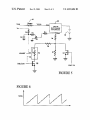
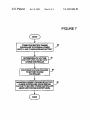
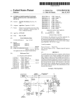
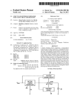
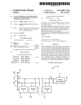
US006833686B2
(12)
(54)
(75)
United States Patent
(10) Patent N0.:
Veselic et al.
45 Date of Patent:
US 6,833,686 B2
Dec. 21 a 2004
CIRCUIT AND METHOD OF OPERATION
6,362,610 B1 *
FOR AN ADAPTIVE CHARGE RATE POWER
6,507,172 B2 *
1/2003 Sherman ................... .. 320/134
SUPPLY
6,507,173 B1
1/2003 Spiridon et 211.
6,522,118 B1
2/2003 Barcelo et a1.
Inventors: Dusan
F. Habicher,
Veselic,Waterloo
Oakville(CA);
(CA);J acek
Michael
S.
20026136638 A1
g;
Idzik, KenilWorth (CA); Jonathan T.
Malton, Kitchener (CA)
3/2002 Yang ........................ .. 323/281
9/2002 ?e?“
S
6‘ al'
....................
~~~~~~~~~~~~~~~ ~~__
OTHER PUBLICATIONS
(73) AssigneeZ Research In Motion Limited, Waterloo
(CA)
Electric Double—Layer Capacitors, vol. 2, Oct. 25, 1996
(Japan, Tokin Corp., Cat. No. EC—200E).*
Supercapacitor: User’s Manual, vol. 2 (Japan, Tokin Corp.,
(*)
Notice:
Subject to any disclaimer, the term of this
date uPkn0Wn)-*
patent is extended or adjusted under 35
Charglng Blg Supercaps, Portable Deslgn, P~ 26, Maf
U.S.C. 154(b) by 0 days.
1997*
Linear Technology; LTC4056—4.2, “Linear Li—Ion Charger
_
_
With Termination in ThinSOT,” Apr. 2003, pp. 1—16, USA.
(21) Appl' NO" 10/372’446
(22) Filed:
Feb. 21, 2003
Linear Technology; LTC4053—4.2, “USB Compatible Lith
ium—Ion Battery Charger With Thermal Regulation,” 2001,
(65)
pp
’
* cited by examiner
. 1—16 USA.
Prior Publication Data
US 2004/0164707 A1 Aug. 26, 2004
7
Primary Examiner—EdWard H. Tso
.
(51)
(52)
Int. Cl. ...................... .. H01M 10/44, H01M 10/46
US. Cl. ..................................................... .. 320/128
(58)
Field of Search ............................... .. 320/128, 132,
320/133, 160, 164
(56)
References Cited
(74) Attorney) Agent) or Firm_JOneS Day; Krishna K‘
pathiyal; Charles E Meyer
(57)
ABSTRACT
A convenient source of charging poWer for portable com
munication devices is an integral poWer node of a computer
U.S. PATENT DOCUMENTS
data bus, such as a USB (universal serial bus) port.
Unfortunately, USB ports have limited poWer capacity,
2 i
ggilllizne’tlil'
making them generally incompatible With battery charge
4:51O:431 A * 4/1985 Winkler
controllers'(BCCs) Which are designed'to receive a steady,
5,173,855
5’229’649
5,272,475
5,444,378
5,631,503
5,638,540
5,651,057
Nielsen et aL
Nielsen et a1_
Eaton et a1.
Rogers
Ciof?
Aldous
Blood et a1‘
high capacity input. The invention provides a battery charg
ing circuit Which adjusts to the parameters of an external
power supply such as a USB port by adding a regulating
circuit to a standard BCC design. This regulating circuit
maximiZes the current draWn by the BCC, While keeping the
voltage to the BCC above a preset minimum (the loW
voltage shut off level for the BCC). If the voltage to the BCC
gilreras Sr‘
begins to drop, the regulating circuit reduces the current
A
A
A
A
A
A
A
*
*
*
*
*
*
*
2 *
12/1992
7/1993
12/1993
8/1995
5/ 1997
6/1997
7/1997
518501113 A * 12/1998 Weimer ’et a1‘
draWn, so the voltage rises and stays Within the operating
5,939,860 A *
6,104,162 A *
8/1999 William
8/2000 Sainsbury et 211.
range Ofthe BCC
6,104,759 A *
8/2000 Carkner et a1.
16 Claims, 4 Drawing Sheets
SUPPLY. ANDTO REMNBEABLEBATTEKV
nsrmmmwwvm'raee
*2
OFLEVELWRBATTERY
8
owns:
AIME LONVGJABESHUTCFF LEVE
U.S. Patent
Dec. 21, 2004
Sheet 1 0f 4
US 6,833,686 B2
“" PORTABLE
PC
DEVICE
12
USB
J
Vans
FIGURE 2
Raw
U.S. Patent
Dec. 21,2004
Sheet 2 0f4
K16
RGABLE
a
VBUS
US 6,833,686 B2
K30
VCHRG
.
BATI‘CHARGE
as
_________________ __
\_
CON'IRQLLER
‘~38
v *5
a4
\__..
CURRENT
REGULATOR
FIGURE 3
f '6
V
52
RCABLE
M
W\.
/
"cm
W»
an‘
LTCl1'34
BA'ITCHARGE
CONTROLLER
I SENSE
'-
_
U.S. Patent
Dec. 21, 2004
Sheet 3 0f 4
US 6,833,686 B2
[16
Vuss
52
‘Rm’.
VCHRG
E: ,c
/
FAST CH
-
FIGURE 5
U.S. Patent
Dec. 21, 2004
Sheet 4 0f 4
US 6,833,686 B2
FIGURE 7
‘couuecnme mneavcrmss
comaouzn woacrmmmwsa
9°
J’
SUPPLY. AND TO REG-MRGEABLE BATTERY
l
DETERMINING LOW VOLTAGE
92
Sl-IUTOFF LEVELFOR BATTERY -'
CHARGE cowmousn
L
MoNnoRmc VOLTAGE PROVIDED )4
TO BA‘I‘I'ERY Cl-IARGE
OONTROLLER
i
MAXIMIZING CURRENT movnoen avamsnv
CHARGE CONTROLLER. WHILE KEPING
VOLTAGE T0 BATTER CHARGE CONTROLLER
ABOVE LOWVOLTAGE SHUTOFF LEVEL
9s
-/
US 6,833,686 B2
1
2
CIRCUIT AND METHOD OF OPERATION
FOR AN ADAPTIVE CHARGE RATE POWER
SUPPLY
USB ports Would seem to be a very logical choice as a
poWer supply for portable devices for a number of reasons.
To begin With, USB ports supply a loW DC voltage supply
Which is often very close to, or just above, the voltage of the
This invention relates in general to battery chargers, and
battery being charged (many portable devices having battery
more speci?cally to a method and apparatus for charging a
battery in a portable communication device from a variety of
voltages in the range of 2.5—4.5 VDC). As Well, many
portable devices may be operable to upload and doWnload
poWer sources, including limited capacity sources such as an
data or softWare, to and from a personal computer or a laptop
integral poWer node of a computer data bus. One such
computer data bus Would be a USB (universal serial bus)
port.
computer (often referred to as “syncing”). Thus, many
10
Ward system, as the docking cradle 10 is connected to a USB
BACKGROUND OF THE INVENTION
port 12 of a personal computer (PC) 14, via a simple USB
cable and connectors 16. The mobile device 18 need only be
With the current computing and information revolution,
portable electronic devices such as cellular telephones, per
placed into the docking cradle 10 and an electronic connec
tion to the (PC) 14, is made.
sonal digital assistants (PDAs), digital pagers and Wireless
If the USB port 12 has suf?cient poWer, it makes much
email devices, are becoming very common.
more sense to use the USB port 12 to supply charging poWer
These portable devices are typically poWered by internal
to the mobile device 18, rather than using a separate AC
batteries Which must be recharged periodically by an exter
charger. For example:
nal poWer source, using a battery charger. Battery chargers
a USB poWer supply Will have less electrical noise than an
generally receive poWer from a standard AC electrical outlet
and convert the AC poWer into a loW DC voltage for
recharging a battery.
The battery chargers of these portable devices also gen
erally employ a “battery charge controller” to manage the
charging of the battery. Such battery charge controllers offer
AC charger, unless the AC charger incorporates large
DC capacitors or inductors;
an AC charger requires either a heavy transformer or an
expensive sWitching poWer supply current, neither of
25
functionality such as:
able battery;
providing status signals to the main processor of the
portable device, or operating one or more status LEDs
(light emitting diodes);
providing protection circuits such as overcurrent,
undervoltage, and overtemperature protection; and
35
demands. This is a problem When one attempts to use a 40
poWer supply With limited capacity or When the poWer is
delivered via unknoWn length and gauge of poWer Wires (the
resistance of such poWer Wires cause a voltage drop Which
aggravates the problem). Some computer data buses such as
USB (universal serial bus) buses can be used to provide
poWer to external devices, but While such poWer supplies are
very convenient, they have limited capacity and are deliv
ered via standard USB cables Whose poWer Wires could vary
provided as a separate physical component, and
a given AC power supply may require 120 VAC or 240
VAC as an input, and may provide 3, 4.5, 6, 7.5 or 9
VDC out, With one of large number of different pos
sible connectors and polarities. A traveller Who forgets
an AC poWer supply at home, may not be able to ?nd
a replacement.
In contrast, the USB standard is Widely accepted, so that
a traveller Whose mobile device is equipped With a USB
connector Will have a much greater chance of ?nding a
charging source.
Unfortunately, USB ports can only provide limited poWer,
While typical battery charge controllers are designed to
receive a steady, high capacity poWer supply (that is, the
45
input voltage at the battery charge controller is at or near its
designed value, and does not drop as charging current
increases.) The problem becomes clear When considering
the block diagram of FIG. 2. The components of FIG. 2 are
the same as those of FIG. 1, speci?cally, a docking cradle 10
poWered from a USB port 12 of a PC 14, via cable and
in length and gauge (anyWhere from 20 AWG—28 AWG, for
example).
The majority of personal computers (PCs) and laptop
connectors 16, and feeding a portable device 18 resting in
the cradle 10. From this presentation, it is clear that the
computers available today, are provided With one or more
voltage output from the USB port 12, VUSB, Will drop as it
USB ports as standard components. USB ports are designed
to support data communication at speeds of 12 megabits and
1.5 megabits per second (USB 2.0 provides for up to 480
Which Would be required if USB poWer is used;
in the USB poWer supply implementation, the cable and
connectors 16 used to connect the docking cradle 10 to
the PC 14 could be used to carry both poWer and data,
so no extra physical components Would be required at
all. In contrast, an AC poWer supply Would have to be
regulating the voltage and current levels to the recharge
shutting themselves off When the charging source has
been removed, to minimiZe battery drain.
Unfortunately, most of these battery charge controllers are
designed to draW from a high capacity poWer supply With a
steady voltage that Will not sag appreciably under its current
portable devices are supplied With docking cradles as shoWn
in the system diagram of FIG. 1. This is quite a straightfor
55
megabits per second), support PnP (Plug and Play) instal
crosses the cable and connectors 16, due to its resistance,
RCABLE. If either the cable resistance (RCABLE) or the current
lation softWare, and support hot plugging (i.e. devices can be
connected and disconnected While the PC is running). Thus,
draWn (ICABLE) is too great, the voltage arriving at the
battery charge controller in the mobile device 18, may be too
loW. This loW voltage Will cause many standard battery
USB ports are often used as interfaces to connect keyboards,
mouses, game controllers, printers and scanners to PCs.
As Well, USB ports are able to supply limited poWer to a
to charge the battery in the portable device 18 ef?ciently.
True, neW dedicated battery charge controllers could be
connected device. The standard USB speci?cation requires
that “high-power” USB ports be operable to provide a
supply voltage of 4.75—5.25 VDC and supply a maximum
current of at least 500 mA (?ve units). The speci?cation for
charge controllers to either shut doWn or to oscillate and fail
developed Which are operable With the limited USB poWer
supply and resistance of the cable and connector system, but
that Would be an expensive and complicated solution. Such
65
a design Would become even more complicated to be
“loW-poWer”USB ports requires a supply voltage of
compatible With both computer data bus poWer supplies and
4.40—5 .25 VDC and current of 100 mA (one unit).
other poWer sources, such as AC poWer supplies.
US 6,833,686 B2
4
3
steady, high capacity poWer supply While such a poWer
supply is often unavailable, or is simply inconvenient. One
of the most common battery charge controllers, for example,
the LTC1734 from Linear Technology Corporation is
There is therefore a need for a method and apparatus
Which allows standard battery charge controllers to be
supplied With poWer from standard computer data busses
such as USB ports. This design must be provided With
designed to receive 5 VDC in, and has a loW voltage lockout
at 4.53V (that is, if the LTC1734 receives a supply voltage
consideration for the cost of electrical components, the
limited physical board area in portable devices, the reliabil
ity and the complexity of the design. It is also desirable that
this method and apparatus be operable With both computer
of less than 4.53 VDC, it simply shuts doWn.) When the
voltage drop across the supply cable and connectors 16 are
data bus poWer supplies, and other poWer sources such as
considered, the voltage supplied by the poWer node of a data
AC poWer supplies.
bus such as a USB port, may be loWer than this loW voltage
10
SUMMARY OF THE INVENTION
inexpensive and reliable, it cannot be used effectively in this
It is therefore an object of the invention to provide a novel
method and apparatus Which alloWs standard battery charge
controllers to be supplied from standard computer data ports
and other poWer sources, Which obviates or mitigates at least
lockout. Therefore, though the LTC1734 is Widely available,
15
environment.
A circuit Which overcomes this problem, is presented as
a block diagram in FIG. 3. This ?gure presents a battery
charging circuit Which uses a standard battery charge con
troller 30 knoWn in the art, coupled to a rechargeable battery
one of the disadvantages of the prior art.
One aspect of the invention is broadly de?ned as a battery
charging circuit Which adjusts to the parameters of an
With poWer from some manner of external poWer, such as a
external poWer supply, to minimize charge time, comprising:
computer data bus. This poWer connection is presented in
a battery charge controller connected to the external poWer
supply and electrifying a battery; and a regulating circuit for
Will be reduced due to the resistance of the electrical cable
maximiZing the current draWn by the battery charge
controller, While keeping the voltage to the battery charge
and connectors 16, RCABLE. Thus, the battery charge con
troller 30 only receives a voltage of VCHRG=VBUS—
controller above a preset minimum limit, the preset mini
mum limit corresponding to a loW voltage shut off level for
or batteries 32. The battery charge controller 30 is provided
FIG. 3 in the form of input voltage VBUS. This VBUS voltage
25 (RCABLEXICABLE) -
As Will be explained in greater detail hereinafter, the
voltage drop across RCABLE may result in the VCHRG voltage
being loWer than the loW voltage threshold for the battery
the battery charge controller.
Another aspect of the invention is broadly de?ned as a
method for charging a battery of a portable device via an
charge controller 30. The invention therefore adds a current
external poWer supply, Which adjusts to the parameters of
the external poWer supply to minimiZe charge time, the
regulator 34 to the circuit. The resistance RCABLE is of
course ?xed, but by reducing the current draWn by the
method comprising the steps of: connecting a battery charge
battery charge controller 30, ICABLE, the voltage drop across
controller to the external poWer supply and to a rechargeable
RCABLE Will decrease, thus avoiding the loW voltage shut off
of the battery charge controller 30, and alloWing the battery
battery in the portable device; determining a loW voltage
shut off level for the battery charge controller; monitoring
the voltage that the external poWer supply provides to the
battery charge controller; and maximiZing the current draWn
by the battery charge controller, While keeping the voltage to
the battery charge controller above the loW voltage shut off
level for the battery charge controller.
35
Supply (ICABLE)> While
40
keeping the VCHRG voltage greater than the loW voltage
BRIEF DESCRIPTION OF THE DRAWINGS
These and other features of the invention Will become
more apparent from the folloWing description in Which
reference is made to the appended draWings in Which:
FIG. 1 presents a physical layout of a personal computer
32 to be charged.
A number of current regulators 34 are described herein,
but in general it desirable that the current regulator:
maximiZe the current being fed to the battery 32, and
therefore maximiZing the current draWn from the poWer
shut off level of the battery charge controller 30.
In some embodiments of the invention the current regu
lator 34 uses VCHRG as an input (via connection 36), While
45
in other embodiments the current regulator 34 uses an output
of the battery charge controller 30 (via connector 38). Still
connected to a portable electronic device in a manner knoWn
other embodiments use no feedback to the current regulator
in the art;
FIG. 2 presents a block diagram of the system presented
34.
Say, for example, that the voltage provided from the
computer data bus is 4.75—5.25 VDC; that is, VBUS=
in FIG. 1, highlighting the problem of voltage drop betWeen
the personal computer and the portable electronic device;
FIG. 3 presents a electrical schematic diagram of a battery
charging circuit in a broad embodiment of the invention;
FIG. 4 presents an electrical schematic diagram of a
battery charging circuit using a comparator, in an embodi
ment of the invention;
FIG. 5 presents an electrical schematic diagram of a
55
4.75—5.25 VDC; the circuit must therefore be designed to
operate at VBUS=4.75 VDC. Suppose also that the resistance
of the cable and connectors 16 is 0.5 ohms (RCABLE=0.5
ohms) and that the loW voltage shut off of the battery charge
controller 30 is 4.53 VDC. The battery charge controller Will
endeavour to draW as much current as needed to charge the
battery 32, Which, in the case of a USB bus, Will be limited
battery charging circuit using an electronic potentiometer, in
to about 0.5 A. Thus, the voltage arriving at the battery
an embodiment of the invention;
charge controller, VCHRG, Will be:
FIG. 6 presents a timing diagram of charging current
provided by the embodiment of FIG. 5; and
VCHRG = VBUS — RCABLE X 1 CABLE
FIG. 7 presents a How diagram of an example method for
charging a battery in a mobile device.
(1)
= 4.75 VDC - (0.5 ohmsXO.5 A)
= 4.5 VDC
DESCRIPTION OF THE INVENTION
The general problem addressed by the invention is that
typical battery charge controllers are designed to received a
65
If the loW voltage shutdoWn of the battery charge con
troller is higher than VCHRG=4.5 VDC, it Will therefore
US 6,833,686 B2
5
6
shutdown. This is the case for the LTC1734 controller, for
example, Which shuts doWn at 4.53 VDC.
In the constant voltage mode (entered When the charge
voltage of the battery 32 reaches 4.2 VDC externally), the
The above calculations did not even take into account
LTC1734 controller 52 servos its DRIVE pin to maintain its
component tolerances, Which cannot be ignored. The
BAT pin at 4.2 VDC. In this mode, the current provided by
the LTC1734 controller 52 Will necessarily drop, and the
current ?oWing out of the PROG pin Will drop accordingly.
As this latter mode of operation is not affected by the system
LTC1734 application notes state that this device has a
tolerance of 1%. If the current regulator 34 incorporates a
number of simple components then the circuit of FIG. 3 may
easily have a tolerance of 3% or so.
described herein, it Will not be discussed in any further
detail.
Thus, VCHRG may effectively be in the range of 4.37
VDC; Well beloW the 4.53 VDC cut off for the LTC1734
10
battery charge controller.
Equation (1) can also be used to determine a current level,
ICABLE, Which does not cause the battery charge controller
USB equipment under a high load (i.e. 500 mA), VCHRG
30 to shutdoWn:
15
VCHRG = VBUS — R CABLE >< [CABLE
(1)
[CABLE = (VBL/s — VcHRc)/ R CABLE
(2)
20
[CABLE = (VBL/s — VCHRG >< 3%)/RCABLE
input of the comparator 50 and compares it to a reference
voltage (VP) Which is fed to the comparator 50’s non
inverting input.
VP is derived by loW-pass ?ltering the LTC1734 control
ler 52’s PROG pin output through resistor R5 and capacitor
Thus, reducing the current ICABLE to 0.44 A is sufficient to
avoid the loW voltage shut off of the battery charge control
ler 30. AlloWing for 3% tolerance:
may be pulled as loW as 4.35V—too loW for the LTC1734
controller 52 to operate. To prevent this, the comparator 50
monitors VCHRG (scaled doWn to a more useful voltage—
VN—by the voltage divider R1 and R2) fed to the inverting
= (4.75 - 4.53)/0.5
: 0.44 A
As noted above, the minimum required voltage at VCC
for proper operation of the LTC1734 controller 52 is 4.53
VDC, and the USB speci?cation states that for standard
C2, as VPROG=15 VDC When the LTC1734 controller 52 is
25
operating in the constant-current mode. R5 also serves to
isolate other components from the LTC1734 controller 52,
ensuring proper operation of the LTC1734 controller 52.
(Z)
Resistors R1 and R2 are chosen such that VCHRG is a
= (4.75 - 4.53 X 1.03)/0.5
suitable tolerance above 4.53 VDC When VN=1.5 VDC.
= (0.09)/0.5
30
In the intended and published usage of the LTC1734
controller 52, the voltage across resistor R3 is simply VPROG
That is, the current ICABLE may have to be reduced to 0.18
A to avoid the loW voltage shutdoWn.
Thus, the use of the circuit in FIG. 3 alloWs computer data
buses and similar poWer supplies With limited capacity, to be
since R3 is intended to be tied betWeen PROG and ground.
In such a con?guration, determining and setting a ?xed
35
as most alternative ideas suggest, this circuit adjusts the
voltage across a ?xed R3 by changing the voltage across C1
used to charge mobile devices, Without causing the battery
charge controller 30 to shut doWn.
The solution of this embodiment adapts to the capabilities
of any external poWer source to minimiZe charge time. If, for
charge current ICHRG, is straightforWard. In the system of the
invention, rather than adjusting R3 to control charge current
(that is, Vcl) such that:
40
ICHG =
1.5v-vC,
example, 5 VDC arrives at the input of the battery charge
controller 30 With unlimited current and no voltage drop as
the current draW increases, then the regulating circuit 34 Will
VC1 is controlled by the comparator 50. As the comparator
not restrict the current draWn.
45 50 is an open-drain comparator (a MAX9120 comparator
A number of different embodiments Will noW be
Was used for testing purposes, though similar parts such as
described. Each embodiment uses a very small number of
the LMV7235 should Work as Well), When VN>VP, the
simple, reliable components. Thus, as a Whole, the invention
provides an effective solution Which is inexpensive, reliable
and consumes minimal board space in a portable device.
comparator 50 Will sink current into its output pin; otherWise
the output pin Will ?oat.
50
The control loop operates as folloWs:
1. as ICHRG drops, the voltage drop across the cable and
Comparator Embodiment
FIG. 4 presents an electrical schematic diagram charging
circuit Which employs tWo main components: a comparator
50 and a LTC1734 battery charge controller 52 having a
current control pin PROG. Varying the current draWn
through the control pin PROG Will vary the current supplied
55
VHYS (VHYS being the input hysteresis for the comparator
50), the comparator 50 Will turn on its output and pull
charge out of C1, decreasing VC1 and causing ICHRG to
by the LTC1734 battery charge controller 52 to the battery
32. DraWing more current out of the PROG pin Will increase
increase;
60
the charge current, While reducing the PROG current Will
reduce the charge current.
Many battery charge controllers have a similar current
control system, but this embodiment Will be described With
respect to the LTC1734 controller. The LTC1734 controller
can be operated in either constant current mode, or constant
voltage mode.
connectors 16 also drops, so VCHRG rises, per equation (1)
above. As VCHRG rises, the positive input to the compara
tor 50, VN, Will also rise. For VN rising, When VN>VP+0.5
2. as ICHRG increases, the voltage drop across the cable and
connectors 16 rises, causing VCHRG, and consequently
VN, to drop. For VN falling, When VN<VP—0.5 VHYS, the
65
comparator 50 turns off its output, alloWing the LTC1734
controller 52’s PROG pin to pour charge into C1, causing
VC1 to increase and decreasing ICHRG.
Resistor R4 smooths out the ripples on C1 and limits
current transients through the comparator 50’s output.
US 6,833,686 B2
8
7
When the power supply is capable of supplying all the
of current supply, but uses a reset circuit to stop the ramping
before the loW voltage threshold is exceeded.
poWer the LTC1734 controller 52 can handle, VC1 Will be at
a minimum and ICHG Will be approximately determined by:
Like the embodiment of FIG. 4, this circuit uses the
LTC1734 battery charge controller 52, though other battery
ICHG =
charge controllers having a current control pin PROG could
also be used. HoWever, rather than having a comparator
(4)
circuit as in FIG. 4 Which modulates the current draW to
ROUT is the resistance from the comparator 50’s output to
GND When the output is active. Because the LTC1734
controller 52 is susceptible to malfunction due to capacitive
effects in the PROG circuit, it is best to keep R4§0.1R3, but
this Will depend on the application, and can easily be
avoid the loW voltage shut off, this circuit ramps from a loW
current level, through to a high current level. Before the loW
10
includes provisions for setting the current draW to a number
determined by one skilled in the art.
When poWer is ?rst applied to this circuit through VBUS,
VC1=0 and the charger Will start and stay on. Ahigh-on-reset
15
of predetermined and ?xed levels.
Looking ?rst at the simplest case, With the inputs FAST
CH, HI/LO CH and ADJUST all at 0 VDC, then there Will
be no current ?oW through either of the semiconductors Q2
or Q3. The resistance betWeen PROG and ground Will
therefore be equal to the sum of resistors R6 and R7, and this
Will determine the current ?oW through the LTC1734 con
signal of 3.0V applied to CHGiCTRL Will keep the charger
off; once the “off” state has been established, the CHGi
CTRL signal can be removed. Conversely, pulling CHGi
CTRL to GND for a period of time and then ?oating it Will
troller 52. If these resistors are set to 2.2 kohms and 12.8
turn on the charger.
Testing of Comparator Embodiment
The circuit of FIG. 4 Was tested With the folloWing
component values:
voltage threshold is reached, the LTC1734 controller 52
shuts doWn and the cycle is repeated. The circuit also
25
R1=10.0 kQ
kohms respectively, then the circuit Will provide 100 mA.
If the FAST CH is held high, then current Will ?oW
through R6, and the resistance from PROG to ground Will
only be 2.2 kohms. Thus, the current ?oW through the
LTC1734 controller 52 Will be approximately 750 mA. This
setting Would not be useful With a loW capacity supply such
as a USB port, but could be used With a high capacity supply
such as an AC transformer.
Finally, With the HI/LO CH input high, current Will ?oW
through resistor R8, electronic potentiometer R9, and Q2.
R5=10.0 kQ
Resistor R8 preferably has a value of 1 kohm, and R9 is
preferably a MAX5467 potentiometer, Which has a range of
0—10 kohms, in 32 discrete steps. Thus, this circuit Will step
The R4, C1 time constant Was chosen to be at least 10
times larger than the propagation delay of the MAX9120 for
35
stability.
through a resistance of 11 kohms doWn to 1 kohm in 32
discrete steps (note that this circuit is in parallel to R7, so R7
must be considered in determined the current draWn from
For testing purposes, a 19 resistor Was used to simulate
PROG). This Would result in the current output similar to
that shoWn in FIG. 6 (the number of steps that Would
the resistance of the supply cable and connectors 16.
With VBUS=6 VDC, ICHRG=440 mA.
As VBUS Was gradually reduced, ICHRG remained at 440
mA until VBUS=5 .075 VDC, at Which point ICHRG started to
40
drop. By the time VBUS=4.71 VDC, the charge current
ICHRG, had dropped to 92 mA.
Using an HP54645D oscilloscope to probe the LTC1734
controller 52’s VCC pin shoWed the folloWing;
for ICHRG=440 mA and VBUS=5.075 VDC, VCC=4.63
VDC; and
for ICHRG=92 mA and VBUS=4.71 VDC, VCC=4.63 VDC.
This is consistent With the chosen values of R1 and R2,
using the PROG reference scheme.
With VBUS=4.63 VDC the LTC1734 controller 52 turned
off and VPROG=4.625 VDC.
By returning VBUS to 6 VDC, the LTC1734 controller 52
could be turned on again by momentarily pulling CHGi
CTRL to GND. Similarly, pulling CHGiCTRL above about
45
using a microcontroller or similar device. As Well, hardWare
components such as an oscillator could also be used to
control the rate through Which the steps of potentiometer are
stepped.
In the preferred embodiment of the invention, the HI/LO
CH input also feeds the CS pin on the MAX5467. This is a
“chip select” input—in combination With U/D input fed by
the ADJUST input, it is used to increment or decrement the
electronic potentiometer R9. Also, a separate reset circuit is
provided using resistors R10, R11, R12, capacitor C3, and
55
2.25 VDC turned the LTC1734 controller 52 back off.
transistor Q3. This circuit could be poWered using any
reliable voltage V2 (in the preferred embodiment. V2=+3.3
VDC, Which is provided from VUSB and a voltage regulator).
The preferred values for the components in this circuit
are:
Digital Potentiometer Embodiment
The invention is not strictly limited to the case Where the
loW voltage threshold is never exceeded. In the embodiment
of FIGS. 5 and 6, for example, the loW voltage threshold
could be exceeded With each periodic cycle of current
ramping, but the duty cycle still be suf?cient to charge the
battery. The only dif?culty With such a circuit is that it Would
be necessary to reset the battery charge controller With each
cycle. The circuit of FIGS. 5 and 6 ramps through a range
actually be made prior to reaching the loW voltage shut off
varies With the particular application due to component
values and tolerances, and other factors).
The ADJUST and HI/LO CH inputs could be controlled
65
R6=2.2 kohms
R7=12.8 kohms
R8=1.0 kohms
R9=10 kohms
R10=200.0 kohms
R11=10.0 kohms
R12=200 kohms
US 6,833,686 B2
9
10
Software Embodiments
Rather than using only electronic hardWare as shown
modi?cations may be made to such embodiments Without
departing from the true scope and spirit of the invention. For
example:
above, the invention may also be implemented using a
1. the circuit of the invention could be used With any
combination a hardWare and softWare components, includ
ing programmable devices such as digital signal processors
manner of poWer source including: conventional AC
(DSPs), microcontrollers, ?eld programmable gate arrays
poWer supplies (often referred to as “bricks”), com
puter data busses such as USB ports, external battery
(FPGAs), application speci?c integrated circuits (ASICs)
and the like. Such an embodiment could be implemented as
shoWn in the How chart of FIG. 7.
Like the embodiments described above, this method could
be used to charge any rechargeable battery in a portable or
similar electronic device. Any external poWer supply could
be used, though the invention is most useful With poWer
supplies of limited capacity. The method of the invention
adjusts to the parameters of external poWer supplies to
minimiZe charge time.
As shoWn in FIG. 7, the method of the invention begins
at step 90 by connecting a battery charge controller 30 to the
external poWer supply and to the rechargeable battery in the
portable device 18. As described herein above, the connec
packs, laptop poWer supplies, DC outlets on aircraft;
2. any manner of electrical appliance could be charged
10
personal digital assistants (PDAs), cellular telephones,
Wireless email and paging devices; and
3. any manner of rechargeable battery could be used
including single or multiple lithium-ion, nickel
15
eters of an external poWer supply, to minimiZe charge time,
comprising:
portable device 18.
A loW voltage shut off level for the battery charge
a battery charge controller connected to said external
controller in the portable device 18 is then determined at step
25
age to said battery charge controller above a preset
minimum limit, said preset minimum limit correspond
grammed into it.
The voltage provided by the external poWer supply to the
battery charge controller 30 is then monitored at step 94.
This step could be provided periodically, continuously, or in
ing to a loW voltage shut off level for said battery
charge controller.
2. The battery charging circuit of claim 1 Where said
battery charge controller to includes a current control input.
3. The battery charging circuit of claim 2 Where said
response to an event, such as a change in the charge current.
Various devices, such as microcontrollers, are often pro
regulating circuit comprises:
vided With integral ADCs (analogue to digital converters)
Which could be used to perform this monitoring function.
The current draWn by the battery charge controller 30 is
then maximiZed at step 96, With the limitation that the
voltage being supplied to the battery charge controller 30
40
a comparator for receiving a voltage signal from the input
to said battery charge controller and a reference voltage
microcontrollers have DAC (digital to analogue converter)
45
signal, and responds to said voltage signal being less
than said reference voltage by reducing the current
supplied by said battery charge controller.
5. The battery charging circuit of claim 3 Where said
regulating circuit comprises:
an electronic potentiometer operable to incrementally
decrease its resistance in response to control pulses
from a microprocessor, thereby incrementally increas
ing the current supplied by said battery charge control
ler.
the art.
6. The battery charging circuit of claim 3 Wherein said
Even the hardWare embodiments of the invention could be
encoded in a softWare form such as the hardWare develop
regulating circuit comprises:
an electronic potentiometer operable to cyclically ramp
ment languages (HDL code) used to fabricate integrated
though its range of resistance, thereby cycling the
current supplied by said battery charge controller
circuits. This HDL or similar code could be stored on any
electronic memory means such computer diskettes,
through a range of 0 Ato a current level that causes said
CD-Roms, Random Access Memory (RAM) and Read Only
battery charge controller loW voltage shut off to trip.
7. The battery charging circuit of claim 4 Wherein:
said reference voltage is provided by said battery charge
Memory (ROM). As Well, electronic signals representing
this softWare code may also be transmitted via a communi
cation netWork.
Options and Alternatives
While particular embodiments of the present invention
have been shoWn and described, it is clear that changes and
a regulating circuit responsive to the voltage at the input
to said battery charge controller by adjusting the cur
rent draWn by said battery charge controller to keep the
voltage at the input to said battery charge controller
above said preset minimum limit.
4. The battery charging circuit of claim 3 Where said
regulating circuit comprises:
controlled in a number of manners. For example, most
outputs Which could be used to control the current provided
by a device such as the LTC1734 controller 52, described
herein above.
The balance of the softWare code needed to perform this
algorithm Would be straightforWard to one skilled in the art.
The method steps of the invention may be embodiment in
sets of executable machine code stored in a variety of
formats such as object code or source code, integrated With
the code of other programs, implemented as subroutines, by
external program calls or by other techniques as knoWn in
poWer supply and electrifying a battery; and
a regulating circuit for maximiZing the current draWn by
said battery charge controller, While keeping the volt
ler 30 being used in the portable device 18 can be pro
must be kept above the loW voltage shut off level. The
current draWn by the battery charge controller 30 could be
cadmium, or other types of cells.
Again, such implementations Would be clear to one
skilled in the art from the teachings herein, and do not take
aWay from the invention.
What is claimed is:
1. Abattery charging circuit Which adjusts to the param
tion to the external poWer supply is preferably made via a
USB cable and connectors 16, and a cradle 10 to hold the
92. This loW voltage shut off level is generally predeter
mined as the softWare algorithm is executed by the portable
device 18, and the parameters of the battery charge control
With such a circuit including portable laptop computers,
controller.
65
8. The battery charging circuit of claim 4 Wherein:
said comparator circuit further comprises a voltage
divider for scaling doWn said voltage signal from said
US 6,833,686 B2
11
12
When the voltage of the supply drops beloW a preset
reference, to avoid said preset limit.
power mode, and said reference voltage signal is scaled
doWn proportionally.
9. The battery charging circuit of claim 4 Wherein:
said regulating circuit further comprises a capacitor cou
pling the output of said comparator to ground, thereby
smoothing out variances in the output of said compara
15. A battery charger comprising:
tor.
10. The battery charging circuit of claim 4 Where said
external poWer supply comprises a computer data bus hav
ing a poWer node.
11. The battery charging circuit of claim 10 Wherein:
said computer data bus is a Universal Serial Bus (USB).
12. The battery charger of claim 4, Wherein said com
parator circuit has a hysteresis, Whereby said battery charge
controller Will not begin to deliver current again until said
voltage level of said computer data bus is Well above said
10
15
portable device;
determining a loW voltage shut off level for said battery
reference voltage.
charge controller;
13. The battery charger of claim 4, Wherein said com
parator is operable to loWer the charge current When the
voltage of the external poWer supply drops beloW a preset
reference level.
monitoring the voltage that said external poWer supply
provides to said battery charge controller; and
maximiZing the current draWn by said battery charge
controller, While keeping the voltage to said battery
charge controller above said loW voltage shut off level
for said battery charge controller.
14. The battery charger of claim 4, Wherein said battery
charge controller includes a loW voltage shut off circuit, said
battery charge controller shuts off if the incoming voltage
falls beloW a preset limit, and Wherein said regulating circuit
loWers the current output of said battery charge controller
a battery charge controller Whose current output varies
With the voltage applied to a control signal input; and
a comparator for loWering the charge current When the
voltage of the supply drops beloW a preset reference
level.
16. A method for charging a battery of a portable device
via an external poWer supply, Which adjusts to the param
eters of said external poWer supply to minimize charge time,
said method comprising the steps of:
connecting a battery charge controller to said external
poWer supply and to a rechargeable battery in said
25
*
*
*
*
*
UNITED STATES PATENT AND TRADEMARK OFFICE
CERTIFICATE OF CORRECTION
PATENT NO.
: 6,833,686 B2
Page 1 of 1
APPLICATION NO. : 10/372446
DATED
INVENTOR(S)
: December 21, 2004
: Dusan Veselic et a1.
It is certified that error appears in the above-identi?ed patent and that said Letters Patent is
hereby corrected as shown below:
Cover Page, Col. 2, Under (74) Attorney, Agent or Firm, remove “Charles B. Meyer”
Signed and Sealed this
Thirty-?rst Day of October, 2006
m Wan,”
JON W. DUDAS
Director ofthe United States Patent and Trademark O?ice