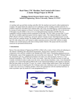
1
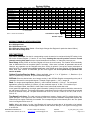
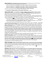
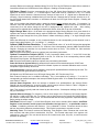
Model PCI-76CS2
Twelve (12) S/D Channels
Twelve (12) S/D
Single Speed or Two-Speed, Programmable
Multi-Speed Ratios: 2 to 255
Continuous Self-Test;
On-Board Programmable Reference Supply (Optional)
FEATURES:
•
•
•
•
•
•
•
•
•
•
•
•
•
•
•
16 bit resolution
1 arc minute accuracy
Continuous background bit testing with Reference and Signal loss detection
Power-On Self-Test (POST)
S/D channels are self-calibrating
Automatically supports either 5V or 3.3V PCI bus
47 Hz to 10 kHz Variations available
Encoder (A & B) plus Index Outputs with Programmable resolution-Optional
Synchro/Resolver Programmable-Optional (Measurement side S/D)
Transformer isolated
Accurate Digital Velocity outputs
Latch feature
Synthetic reference for S/D compensates for ±60° phase shift
No adjustments or trimming required
Part number, S/N, Date code, & Rev. in non-volatile memory
DESCRIPTION:
This single slot card contains separate transformer isolated Synchro/Resolver-to-Digital tracking
converters, optional internal 5 VA reference, and extensive diagnostics. The measurement channels
incorporate Synchro/Resolver inputs, high linearity digital velocity outputs, angle change alert and
ability to field configure for either single speed or multi-speed to any ratio between 2 and 255. The S/D
channels, even when large accelerations are encountered, never lose tracking, because they incorporate the
unique capability to automatically shift to higher bandwidths. The shifting is smooth and continuous with no
glitches. Tracking rates are only limited to bandwidth restrictions, up to 150 RPS, at 16-bit resolution. The
“Latch” feature permits the user to read all channels at the same time. The use of Type II servo loop processing
techniques enables tracking, at full accuracy, up to the specified tracking rate. A step input will not cause any
hang-up condition. Intermediate transparent latches, assure that current valid data is always available for any
channel without effecting the tracking performance of the converters. For two-speed applications, our ambiguity
circuits maintain monotonic outputs by compensating for variations of the zero positions between the Coarse
and Fine Synchros. However, if the maximum allowable angle difference of 90°/n is exceeded, a flag will be set
that indicates to the user that the input Synchro’s are out of alignment. To simplify logistics, Part number, S/N,
Date code, & Rev. are located in non-volatile memory locations.
Major diagnostics are incorporated that offer substantial improvements to system reliability because user is
immediately alerted to channel malfunctions. This approach also reduces bus traffic because the Status
Registers do not require constant polling. Power-On, Self-Test (POST) diagnostic can immediately initiate (D3)
test.
See Programming Instructions for further details.
Three different tests (one on-line and two off-line) can be selected:
The (D2) test for measurement channels initiates automatic background bit testing. Each channel is checked
every 5° to a test accuracy of 0.05°. Any failure triggers an Interrupt (if enabled) and the results are available in
the S/D Test Status Registers. The testing is totally transparent to the user, requires no external programming,
has no effect on the standard operation of this card and can be enabled or disabled via the bus.
North Atlantic Industries, Inc.
110 Wilbur Place, Bohemia, NY 11716
631.567.1100/631.567.1823 (fax)
www.naii.com / e-mail:[email protected]
6/29/2004
Cage Code:OVGU1
76_CS2_A001_Rev_1.9.docc
Page 1 of 11
In addition, each S/D Signal and Reference input is continually monitored. Any failure triggers an Interrupt (if
enabled) and the results are available in the S/D Signal and Reference Status Registers.
The (D3) or POST test, (if enabled), is an initiated bit test that disconnects all input channels from the outside
and connects them across internal test signals that generate and test 72 different angles to a test accuracy of
0.05°. External reference is not required. Any failure triggers an Interrupt (if enabled). Testing requires no
external programming, and can be enabled or disabled via the bus.
The (D0) test is used to check the card and the interface. All input channels are disconnected from the outside
and connected across the internal test signals, thus allowing user to write any angle to the card and then read
the data from the interface. External reference is not required.
SPECIFICATIONS:
Applies to each Measurement channel
Resolution:
Accuracy:
16 bit (Up to 24 bit for two-speed mode)
±1 arc minute for single speed inputs
(±1 arc minute divided by gear ratio for two-speed)
18.5 RPS for 60 Hz version; 150 RPS for 360 Hz or greater versions. (Referred to the Fine
input for two-speed configuration)
10 Hz for 60 Hz versions; 40 Hz for 400 Hz versions, & 100 Hz for greater than 1 kHz
version. (also can be factory customized)
Synchro or Resolver, (See part number)
Resolver : 2-28 V L-L Autoranging, or 90 V L-L
Synchro : 11.8 V L-L , or 90 V L-L
Resolver and Synchro are transformer isolated
Other input options available; consult factory.
26 V L-L or less: 40 kΩ min. 90 V L-L: 100 kΩ min.
2-115 Vrms, @ 5 ma max ; Transformer isolated. (See part number)
47 Hz to 10 kHz (See part number)
Either 12,13,14,15, or 16-bit resolution, (field programmable) with Index marker. 12-bit
resolution is equivalent to 1,024 cycles (4,096 transitions), 13-bit is 2,048 cycles (8,192
transitions) etc. After the encoder resolution has been selected, (12-16 Bits), it will not
change with varying input speeds. Differential outputs are complementary TTL (use TTL+
and dc gnd for short distances or TTL(+) and (–) in the differential mode, into differential
receivers for long distance to avoid ground noise ). Optional, see P/N.
Equivalent to the A, B, C outputs from Hall Effect Sensors for 4, 6 or 8 pole motors
The synthetic reference circuit automatically compensates for phase shifts between the
transducer excitation and output up to ±60°
16 bit resolution; Linearity: 0.1%
Programmable from 2 to 255.
Each channel can be set to a different angle differential. When that differential is exceeded,
an interrupt is generated. Default is disabled. Msb = 180°; Minimum differential is 0.05°. Max
differential that can be programmed is 179.9°.
Tracking Rate:
Bandwidth:
Input format:
Input voltage:
Input Impedance:
Reference/Input:
Frequency:
Encoder outputs:
Commutation outputs:
Phase shift:
Velocity, Digital:
Two-speed ratio:
Angle change alert:
REFERENCE SUPPLY:
Optional. (See part number).
Voltage:
2.0-28Vrms programmable, resolution 0.1Vrms, or 115Vrms fixed.
Accuracy ±2%
360 Hz to 10 kHz ±1% with 1 Hz resolution.
10% max. No load to full load.
5VA max. @ 40° min. inductive;
190mA RMS @ 2-26VAC, 45mA RMS @ 115VAC
Note: Power is reduced linearly as the Reference Voltage.
Frequency:
Regulation:
Output power:
GENERAL SPECIFICATIONS:
Signal Logic Level:
Power:
Temperature, operating:
Temperature, storage:
Size:
Weight:
North Atlantic Industries, Inc.
110 Wilbur Place, Bohemia, NY 11716
Automatically supports either 5V or 3.3V PCI bus.
See current requirement Table 1 below. Power supplies must be able to supply the peak
power without current limiting.
“C” = 0°C to +70°C, “E” = -40°C to +85°C (See part number)
-55° C to +105° C
3.950 (10.033) height, 12.285 (31.204) length; less front panel connector J1;
dimensioned in inches (cm)
Board & heat sink less modules
10 oz. Max.
S/D modules @ 4 Ch ea.
2.5 oz. Max.
Reference module
1.8 oz. Max.
631.567.1100/631.567.1823 (fax)
www.naii.com / e-mail:[email protected]
6/29/2004
Cage Code:OVGU1
76_CS2_A001_Rev_1.9.doc
Page 2 of 11
CURRENT REQUIREMENTS:
±12Vdc
15mA
15mA
Board – no Modules
Add per 4 Ch S/D Mod
Reference Module
+5Vdc
460mA
160mA
1A @ 5VA Load (3A Peak)
TABLE 1
PROGRAMMING INSTRUCTIONS AND REGISTER MAP
000
004
008
00C
010
014
018
01C
020
024
028
02C
030
034
038
03C
040
044
048
04C
050
054
058
05C
060
064
068
06C
070
074
078
07C
080
084
088
08C
090
094
098
09C
0A0
0A4
0A8
S/D Ch.1 Data
1
S/D Ch.2 Data Hi
S/D Ch.3 Data
1
S/D Ch.4 Data Hi
S/D Ch.5 Data
1
S/D Ch.6 Data Hi
S/D Ch.7 Data
1
S/D Ch.8 Data Hi
S/D Ch.9 Data
1
S/D Ch.10 Data Hi
S/D Ch.11 Data
1
S/D Ch.12 Data Hi
Velocity, S/D Ch.1
Velocity, S/D Ch.2
Velocity, S/D Ch.3
Velocity, S/D Ch.4
Velocity, S/D Ch.5
Velocity, S/D Ch.6
Velocity, S/D Ch.7
Velocity, S/D Ch.8
Velocity, S/D Ch.9
Velocity, S/D Ch.10
Velocity, S/D Ch.11
Velocity, S/D Ch.12
Ratio S/D Ch.1/2
Ratio S/D Ch.3/4
Ratio S/D Ch.5/6
Ratio S/D Ch.7/8
Ratio S/D Ch.9/10
Ratio S/D Ch.11/12
Angle Δ Ch.1
Angle Δ Ch.2
Angle Δ Ch.3
Angle Δ Ch.4
Angle Δ Ch.5
Angle Δ Ch.6
Angle Δ Ch.7
Angle Δ Ch.8
Angle Δ Ch.9
Angle Δ Ch.10
Angle Δ Ch.11
Angle Δ Ch.12
Angle Δ initiate
read
read
read
read
read
read
read
read
read
read
read
read
read
read
read
read
read
read
read
read
read
read
read
read
read/write
read/write
read/write
read/write
read/write
read/write
read/write
read/write
read/write
read/write
read/write
read/write
read/write
read/write
read/write
read/write
read/write
read/write
write
0AC
0B0
0B4
0B8
0BC
0C0
0C4
0C8
0CC
0D0
0D4
0D8
0DC
0E0
0E4
0E8
0EC
0F0
0F4
0F8
0FC
100
104
108
10C
110
114
118
11C
120
124
128
12C
130
134
138
13C
140
144
148
14C
150
154
Active channels, S/D
Test (D2) verify, S/D
Test Enable, S/D
Status, Signal S/D
Status, Reference S/D
Status, Test S/D
Latch
S/D Test angle
Angle Δ alert
Synchro/Resolver
Lock loss
(A&B) resolution/poles Ch. 1
(A&B) resolution/poles Ch. 2
(A&B) resolution/poles Ch. 3
(A&B) resolution/poles Ch. 4
(A&B) resolution/poles Ch. 5
(A&B) resolution/poles Ch. 6
(A&B) resolution/poles Ch. 7
(A&B) resolution/poles Ch. 8
(A&B) resolution/poles Ch. 9
(A&B) resolution/poles Ch. 10
(A&B) resolution/poles Ch. 11
(A&B) resolution/poles Ch. 12
Velocity, S/D scale Ch.1
Velocity, S/D scale Ch.2
Velocity, S/D scale Ch.3
Velocity, S/D scale Ch.4
Velocity, S/D scale Ch.5
Velocity, S/D scale Ch.6
Velocity, S/D scale Ch.7
Velocity, S/D scale Ch.8
Velocity, S/D scale Ch.9
Velocity, S/D scale Ch.10
Velocity, S/D scale Ch.11
Velocity, S/D scale Ch.12
1
S/D Ch.2 Data Lo
1
S/D Ch.4 Data Lo
1
S/D Ch.6 Data Lo
1
S/D Ch.8 Data Lo
1
S/D Ch.10 Data Lo
1
S/D Ch.12 Data Lo
Not Used
Not Used
TABLE 2
read/write
read/write
read/write
read
read
read
write
read/write
read
read/write
read
read/write
read/write
read/write
read/write
read/write
read/write
read/write
read/write
read/write
read/write
read/write
read/write
read/write
read/write
read/write
read/write
read/write
read/write
read/write
read/write
read/write
read/write
read/write
read/write
read
read
read
read
read
read
158 Not Used
15C Not Used
160 Not Used
164 Not Used
168 Not Used
16C Not Used
170 Not Used
174 Not Used
178 Not Used
17C Not Used
180 Not Used
184 Not Used
188 Not Used
18C Not Used
190 Not Used
194 Not Used
198 Not Used
19C Not Used
1A0 Not Used
1A4 Not Used
1A8 Not Used
1AC Not Used
1B0 Not Used
1B4 Not Used
1B8 Not Used
1BC Not Used
1C0 Not Used
1C4 Interrupt Enable
1C8 Interrupt Status
1CC Freq. (Ref. Supply)
1D0 Voltage (Ref. Supply)
1D4 Watchdog timer
1D8 Soft reset
1DC Part #
1E0 Serial #
1E4 Date code
1E8 Rev level PCB
1EC Rev. level S/D DSP Master
1F0 Rev. level S/D FPGA Master
1F4 Rev. level S/D DSP Slave
1F8 Rev. level S/D FPGA Slave
1FC Rev. level Interface FPGA
200 Board Ready
read/write
read
read/write
read/write
read/write
write
read
read
read
read
read
read
read
read
read
read
Note 1 – Read channels (2,4,6,8,etc.) for combined 16-bit output. For 24 bit resolution, read Hi then Lo word.
When read, Hi word latches Lo word.
North Atlantic Industries, Inc.
110 Wilbur Place, Bohemia, NY 11716
631.567.1100/631.567.1823 (fax)
www.naii.com / e-mail:[email protected]
6/29/2004
Cage Code:OVGU1
76_CS2_A001_Rev_1.9.doc
Page 3 of 11
Register Bit Map
D15
D14
D13
D12
1
180
90
45
22.5
Data (angle)° Hi
1
.00274 .00137 .00068 .00034
Data (angle)° Lo
Active channels, S/D
X
X
X
X
Latch outputs
X
X
X
X
X
Two-speed lock loss
X
X
X
Synchro/Resolver
X
X
X
X
X
X
X
X
Test Enable, S/D
Status, Test S/D
X
X
X
X
Status, Signal S/D
X
X
X
X
X
X
X
X
Status, Reference S/D
X
X
X
X
Angle Δ Alert S/D
Interrupt Enable/Status
X
X
X
X
(A&B) resolution/poles D15
X
X
X
↑ "0"= Encoder
"1"= Commutation
Note 1 –Values are rounded off.
D11
11.25
.00017
SD12
X
11/12
SD12
X
SD12
SD12
SD12
SD12
X
X
D10
D9
D8
D7
5.625 2.813 1.406 .703
.00008.00004.00002 0
SD11 SD10 SD9 SD8
X
X
X
X
X
X Ch7/8
9/10
SD11 SD10 SD9 SD8
X
X
X
X
SD11 SD10 SD9 SD8
SD11 SD10 SD9 SD8
SD11 SD10 SD9 SD8
SD11 SD10 SD9 SD8
#7
#6
#5
X
X
X
X
X
D6
.352
0
SD7
X
X
SD7
X
SD7
SD7
SD7
SD7
X
X
D5
D4
D3
.176
.088
.044
0
0
0
SD6
SD5
SD4
X
X
X
Ch5/6
X
Ch3/4
SD6
SD5
SD4
X
X
D3
SD6
SD5
SD4
SD6
SD5
SD4
SD6
SD5
SD4
SD6
SD5
SD4
X
X
#4
X
X
X
4 pole
16 bit
TABLE 3
6 pole
15 bit
8 pole
14 bit
13 bit
Commutation outputs
↑
12 bit
Encoder outputs
D2
.022
0
SD3
X
X
SD3
D2
SD3
SD3
SD3
SD3
#3
D2
0
0
0
0
1
D1
.011
0
SD2
1
Ch1/2
SD2
X
SD2
SD2
SD2
SD2
#2
D1
0
0
1
1
0
D0
.0055
0
SD1
X
X
SD1
D0
SD1
SD1
SD1
SD1
#1
D0
0
1
0
1
0
↑
INTERRUPT ENABLE & STATUS REGISTERS
#1 = S/D Signal Loss
#2 = S/D Reference Loss
#3 = S/D Angle Change Alert (Global – Read Angle Change Alert Register for particular channel failure)
#4 = S/D Test Accuracy Error
S/D FUNCTIONS
S/D Active Channels: Set the bit corresponding to each channel to be monitored during BIT testing in the
S/D Active Channel Register (“1”=active; “0”=not used). Omitting this step will produce errors on unused
channels causing false alarms; hence unused channels will set faults, i.e. status bits, interrupts, etc.
Save Setup: Writing 5555h to the Save Register will save the current setup. This location will automatically
clear to 0000h when save is completed (within 5 seconds). When save is elected, all parameters are saved.
However, any parameter can be changed at any time. Saving is optional. If not saved, reenter parameters at
each Power-On. To restore factory shipped parameters, write AAAAh to the Save Register, followed by System
Reset. Note: After a SAVE or RESTORE, poll the Save Register and do not perform any operation until
word is at 0000h.
Optional Synchro/Resolver Mode: Where applicable, write a “1” or “0” (Synchro = 1; Resolver = 0) to
each bit, representing a channel, of Synchro/Resolver Register.
S/D Ratio: Enter the desired ratio, as an integer number, in the S/D Ratio Register corresponding to the pair of
channels to be used for a two-speed channel. Example: Single speed = 1; 36:1 = integer 36.
Read: For single speed applications (Ratio=1), read individual channels 1,2,3,4,etc. For two-speed
applications, read only channels (2,4,6,8,etc.) for the combined output of 16 bits. For resolution up to
24 bits, read Data Hi word, then Data Lo word. Data Hi word, when read, latches low word.
In two-speed S/D applications, the single speed information (coarse) from the synchro should be connected to
the odd channel of the pair. The N-speed information (multi-speed, fine) from the synchro should be connected
to the even channel of the pair. The pairs are defined as: CH1 & 2, CH3 & 4, CH5 & 6, CH7 & 8, CH9 & 10, or
CH11 & 12.
Two-Speed Lock-Loss: The card monitors misalignment between Coarse and Fine angles during twospeed operation. A two-speed lock loss condition exists if the maximum allowable misalignment between the
Coarse and Fine angles of 90°/ratio is exceeded. The corresponding bit for that channel pair in the Two-Speed
Lock-Loss Register will be set to “0”.
Latch: Writing the integer 2 to the Latch Register will cause the angle data of all channels to be latched.
Reading a particular channel will disengage the latch for that channel. Writing 0 to this register will disengage latch
on all channels.
North Atlantic Industries, Inc.
110 Wilbur Place, Bohemia, NY 11716
631.567.1100/631.567.1823 (fax)
www.naii.com / e-mail:[email protected]
6/29/2004
Cage Code:OVGU1
76_CS2_A001_Rev_1.9.doc
Page 4 of 11
Velocity Output: Read Velocity Registers of each channel as a 2’s complement word, with 7FFFh being
maximum CW rotation, and 8000h being maximum CCW rotation.
When max. velocity is set to 152.5878 RPS, an actual speed of 10 RPS CW would be read as 0863h.
When max. velocity is set to 152.5878 RPS, an actual speed of 10 RPS CCW would be read as F79Ch.
When max. velocity is set to 50.8626 RPS, an actual speed of 10 RPS CW would be read as 192Ah.
When max. velocity is set to 50.8626 RPS, an actual speed of 10 RPS CCW would be read as E6D5h.
To convert a velocity word to RPS: Velocity in RPS = Maximum x Output / Full Scale
If Velocity Output were E6D5h, and maximum velocity were 50.8626 RPS, then
Velocity in RPS = 50.8626 x E6D5h / 32,768 = 50.8626 x -6,442 / 32,768 = -10 RPS
Velocity Scale Factor: The velocity scale factor is used to achieve a greater resolution at lower
rotational speeds (RPS). The scale factor is: 4095(152.5878RPS/max RPS), where the max RPS is
selected by the user to achieve the maximum resolution for a desired RPS. Enter the scale factor as an
integer to the corresponding Velocity Scale Register for that particular channel.
To scale the Max Velocity word for 152.5878 RPS, set Velocity Scale Factor = 4095 (max velocity word of
+32,767 (7FFFh) being 152.5878 RPS for CW rotation, and -32,768 (8000h) being 152.5878 RPS for CCW
rotation). Scaling effects only the Velocity output word and not the dynamic performance.
To get a maximum velocity word (32,767) @ 152.5878 RPS, Scale Factor = 4095(152.5878/152.5878) = 4095 = 0FFFh;
This results in a velocity resolution of: (152.5878 RPS/32,767) x 360°/RPS = 1.676°/sec
(factory default)
To get a maximum velocity word (32,767) @ 50.8626 RPS, Scale Factor = 4095(152.5878/50.8626) = 12,285 = 2FFDh);
This is a velocity resolution of: (50.8626 RPS/32,767) x 360°/RPS = 0.5588°/sec
For 9.5367 RPS max, Scale Factor = 4095(152.5878/9.5367) = 65,520 = FFF0h; 0.10477 °/sec resolution
(lowest setting)
S/D Power-On Self-Test (POST): The unit will initiate the D3 Test upon power-on, if POST is enabled and
saved. Enable by writing "1" to POST Register. Disable by writing "0" to POST Register and then save setup.
S/D D2 Test Enable: Writing “1” to the D2 bit of the S/D Test Enable Register initiates automatic background
BIT testing that checks each channel every 5° to a test accuracy of 0.05°. The result of an accuracy error is
available in the S/D Test Status Register and if enabled, an interrupt will be generated (See Interrupt Register).
A “0” deactivates this test. The testing is totally transparent to the user, requires no external programming, has
no effect on the standard operation of this card and can be enabled or disabled. The card will write 55h to the
S/D Test (D2) Verify Register, every 30 seconds, when the D2 Test is enabled. User can periodically clear the
Test (D2) Verify Register by writing 00h, waiting 30 seconds, then reading the register again to verify that
background BIT testing is activated.
In addition, each S/D Signal and Reference input is continually monitored. Any failure triggers an Interrupt (if
enabled) and the results are available in the S/D Signal and Reference Status Registers.
S/D D3 Test Enable: Writing “1” to the D3 bit of the S/D Test Enable Register initiates a BIT test that
disconnects all channels from the outside world and connects them across an internal stimulus that generates
and tests 72 different angles to a test accuracy of 0.05°. External reference is not required. The test cycle is
completed within 45 seconds and results can be read from the S/D Test Status Registers when D3 bit changes
from “1” to “0” and if enabled, an interrupt will be generated if a BIT failure is detected (See Interrupt Register).
The testing can be terminated at any time by writing "0" to D3 bit of the S/D Test Enable Register.
Signal and Reference monitoring is disabled during D3 test.
S/D D0 Test Enable: Used to check card and PC interface. Writing “1” to the D0 bit of the S/D Test Enable
Register disconnects all channels from the outside world and connects them to internal test signals, enabling
the user to generate any test angle by writing an integer value, to the S/D Test Angle Register. Data is then
read through the interface (after writing, allow 400 ms before reading). External reference is not required. (e.g.
330° = angle/(360/216) ).
Signal and Reference monitoring is disabled during D0 test.
S/D Status, Test: Check the channel’s corresponding bit of the S/D Test Status Register for status of BIT
testing for each active channel. A ”1” means accuracy passes; A “0” indicates a failure on an active channel.
Channels that are inactive are also set to “0”. (Test cycle takes 45 seconds for accuracy error). Any S/D Test
status failure, transient or intermittent will latch the S/D Test Status Register. Reading will unlatch register.
S/D Status, Reference: Check the channel’s corresponding bit of the S/D Reference Status Register for
status of the reference input for each active channel. A ”1” means Reference ON, a “0” means Reference Loss
on active channels. Channels that are inactive are also set to “0”. (Reference loss is detected within 2
North Atlantic Industries, Inc.
110 Wilbur Place, Bohemia, NY 11716
631.567.1100/631.567.1823 (fax)
www.naii.com / e-mail:[email protected]
6/29/2004
Cage Code:OVGU1
76_CS2_A001_Rev_1.9.doc
Page 5 of 11
seconds). Reference monitoring is disabled during D3 or D0 Test. Any S/D Reference status failure, transient or
intermittent will latch the S/D Reference Status Register. Reading will unlatch register.
S/D Status, Signal: Check the corresponding bit of the S/D Signal Status Register for status of the input
signals for each active channel. A "1" means Signal is valid (level must be a minimum of 2V), a “0” means
Signal loss on active channels. Channels that are inactive are also set to “0”. (Signal loss is detected after 2
seconds). Signal monitoring is disabled during D3 and D0 test. Channels that are inactive are also set to “0”.
Any S/D Signal status failure, transient or intermittent will latch the S/D Signal Status Register. Reading will
unlatch register.
Now, let us consider what happens when a status bit changes before registers are read. For example, if a
reference loss was detected and latched into registers and subsequent scans find that the reference was
reconnected, then this status change will be held in background until registers are read.
After reading,
registers will be updated with the background data within 250ms. Allow 250 ms to scan all channels.
Angle Change Alert: Write a 16-bit word to the appropriate Angle Change Register for a given channel, to
represent the minimum differential change required. MSB=180°; Minimum differential is 0.05°, setting to zero
disables the Angle Change Alert for a given channel. Initiate monitoring by writing “1” to Angle Change Initiate
Register.
When that differential is exceeded, on any monitored channel, the bit corresponding to that channel is set in
Angle Change Alert Register ("0" = no change, "1" = change).
Optional (A&B) Encoder Resolution: To set Encoder Mode, write a “0” to the D15 bit and the appropriate
code for the desired resolution to the D2, D1 & D0 bits of the corresponding channel (A&B) Resolution/Poles
Register. Changing the resolution for any channel can be done on the fly. The default is a 12bit resolution
encoder output. See Table 3.
Note: Encoder/Commutation outputs are optional; see part ordering information.
Optional Commutation Outputs (A,B,C): To set Commutation Mode, write a “1” to the D15 bit and the
appropriate code for the required motor poles to the D2, D1 & D0 bits of the corresponding channel (A&B)
Resolution/Poles Register. See Register Bit map table.
Note: Encoder/Commutation outputs are optional; see part ordering information.
Power On Reset or System Reset: All parameters are restored to last saved setup and, if POST was
previously enabled in last setup, a D3 Test will be initiated. A power on automatic calibration test is run and
completes in approximately 30 seconds.
Interrupt Registers: Interrupts can be enabled to relay specific problems/failures detected by the card. The
problem/failures that generate these interrupts are:
S/D Signal Loss, S/D Reference Loss, S/D Angle Change Alert, S/D Test Accuracy Error,
Each external interrupt can be enabled individually. This is accomplished by writing a “1” to the bit
corresponding to desired interrupts to the Interrupt Enable Register and a “0” to disable those interrupts not
used. Refer to Table 3.
Interrupt Status Registers: When an interrupt is initiated via a problem/failure, the Interrupt Status
Register can be interrogated by a read to identify, which interrupt occurred. Refer to Table 3. Register is
latched when interrupt is generated and unlatched when read.
Note: This register is typically read and cleared by the device driver. Subsequent readings of this register
will give clear status.
Optional Reference Supply: For frequency, write a 16-bit integer to the Frequency Ref Supply Register.
(Ex: 400 Hz = 0190h) with LSB= 1Hz. For voltage, write a 16-bit integer to the Voltage Ref Supply Register.
(Ex: 26Vrms =0104h) with LSB=0.1Vrms. It is recommended that the user program the required frequency
before setting the output voltage.
Soft Reset: Write an integer “1” to Soft Reset Register, then clear to 0 before 50ms elapses. CAUTION:
Register is level sensitive and for proper card operation, the logic level “1”, or pulsewidth, must be
<= 50ms. Considering minimum and maximum, 1 μs < pulsewidth <= 50ms. Processor reboots in about
400 ms, after which calibration procedures begin. This function is equivalent to a power-on reset.
Watchdog Timer: This feature monitors the Watchdog Timer Register. When it detects that a code has
been received, that code will be inverted within 100 µsec. The inverted code stays in the register until
replaced by a new code. The user should look for the inverted code, after 100 µsec, to confirm that the
processor is operating.
North Atlantic Industries, Inc.
110 Wilbur Place, Bohemia, NY 11716
631.567.1100/631.567.1823 (fax)
www.naii.com / e-mail:[email protected]
6/29/2004
Cage Code:OVGU1
76_CS2_A001_Rev_1.9.doc
Page 6 of 11
Part Number: Read as a 16-bit binary word from the Part Number Register. A unique 16 bit code is
assigned to each model number.
Serial Number: Read as a 16-bit binary word from the Serial Number Register. This is the serial number
of that particular board.
Date Code: Read as decimal number from the Date Code Register. Four digits represent YYWW (Year,
Year, Week, Week)
Rev Levels: There are a total of 6 Revision Level Registers, which are listed below. Each register is
defined as 16 bits. The integer value of that particular register corresponds to the actual revision.
Rev level PCB
Rev level S/D DSP Master
Rev level S/D FPGA Master
Rev level S/D DSP Slave
Rev level S/D FPGA Slave
Rev level Interface FPGA
Board Ready: When board initialization is completed (& auto-cal for A/D modules), after as much as 10
seconds, the board is ready for access and the Board Ready register is set High.
Software - PCI Programming
This section provides programmers the information needed for developing drivers other than those supplied.
The following information resides in the PCI configuration registers:
Device ID
Vendor ID
Rev
Subsystem ID
= 7622
= 15AC
= 01
= 000115AC
(hex)
(hex)
(hex)
(hex)
Base Address
= Assigned by the PCI BIOS. Interrogate the PCI BIOS for this information.
Required Address space = 1K for each card.
EXTERNAL +/- 12VDC: (JP6 & JP7)
The card is shipped and configured for operation with +/- 12 VDC power, being supplied from edge connector.
To operate from External +/- 12VDC supplies: On jumper block JP7, remove jumpers 1-2, and 5-6, then reconnect jumpers 3-4 and 7-8. Leave jumper 9 – 10 connected.
Connect external +12 VDC to JP6-4, connect external –12 VDC to JP6-2 and external ground to JP6-1.
Pin JP6-3 has been removed for keying. We recommend customer plug receptacle pin 3 to insure
proper connection and avoid damage.
North Atlantic Industries, Inc.
110 Wilbur Place, Bohemia, NY 11716
631.567.1100/631.567.1823 (fax)
www.naii.com / e-mail:[email protected]
6/29/2004
Cage Code:OVGU1
76_CS2_A001_Rev_1.9.doc
Page 7 of 11
4 3 2 1 JP6
1
2 4
1 3
JP4
26
25
2 4
1 3
JP5
48 50
47 49
2
JP7
9 10
78 59 39 20
COMPONENT SIDE OF BOARD
J1
60 40 21 1
Figure 1
Connector: JP6 Samtec TSW 104-14-L-S
Mate: Amp 87499-4, Keying Plug 86286-1
Pin
1
2
3
4
Function
External Ground
External (-12VDC)
Removed for Keying
External(+12VDC)
TABLE 4
North Atlantic Industries, Inc.
110 Wilbur Place, Bohemia, NY 11716
631.567.1100/631.567.1823 (fax)
www.naii.com / e-mail:[email protected]
6/29/2004
Cage Code:OVGU1
76_CS2_A001_Rev_1.9.doc
Page 8 of 11
12 S/D Channels
Connector: J1 –12 S/D
AMP 748483-5
Mate: AMP 748368-1
Pin Ch.1 S/D
39
S1
58
S2
78
S3
19
S4
38
Rhi
77
RLo
Pin Ch.2 S/D
18
S1
76
S2
S3
57
S4
37
17
Rhi
56
RLo
Pin Ch.3 S/D Pin
36
S1
15
55
S2
73
75
S3
54
16
S4
34
35
Rhi
14
74
RLo
53
Ch.4 S/D
S1
S2
S3
S4
Rhi
RLo
Pin Ch.5 S/D Pin Ch.6 S/D
33
S1
12
S1
52
S2
70
S2
72
S3
51
S3
13
S4
31
S4
32
Rhi
11
Rhi
71
RLo
50
RLo
Pin Ch.7 S/D
30
S1
49
S2
69
S3
10
S4
29
Rhi
68
RLo
Pin Ch.8 S/D
9
S1
67
S2
48
S3
28
S4
8
Rhi
47
RLo
Pin Ch.9 S/D Pin Ch.10 S/D Pin Ch.11 S/D
27
S1
6
S1
24
S1
46
S2
64
S2
43
S2
66
S3
45
S3
63
S3
7
S4
25
S4
4
S4
26
Rhi
5
Rhi
23
Rhi
65
RLo
44
RLo
62
RLo
Pin Ch.12 S/D Pin
3
S1
61
S2
42
S3
1 & 40
CHASSIS
22
S4
21 Int. Exc. Out Hi
2
Rhi
60 Int. Exc. Out Lo
41
RLo
TABLE 5
Encoder/Commutation Outputs
Connector : JP5 Samtec TSW-125-25-T-D-RA
Pin
1
2
3
4
5
6
7
8
9
10
11
12
13
14
Function
A Hi Ch1
A Lo Ch1
B Hi Ch1
B Lo Ch1
IDX Hi Ch1
IDX Lo Ch1
A Hi Ch2
A Lo Ch2
B Hi Ch2
B Lo Ch2
IDX Hi Ch2
IDX Lo Ch2
A Hi Ch3
A Lo Ch3
Pin
15
16
17
18
19
20
21
22
23
24
27
28
29
30
Function
B Hi Ch3
B Lo Ch3
IDX Hi Ch3
IDX Lo Ch3
A Hi Ch4
A Lo Ch4
B Hi Ch4
B Lo Ch4
IDX Hi Ch4
IDX Lo Ch4
A Hi Ch5
A Lo Ch5
B Hi Ch5
B Lo Ch5
Pin
31
32
33
34
35
36
37
38
39
40
41
42
43
44
Function
Pin
IDX Hi Ch5 45
IDX Lo Ch5 46
A Hi Ch6
47
A Lo Ch6
48
B Hi Ch6
49
B Lo Ch6
50
IDX Hi Ch6
IDX Lo Ch6 25
A Hi Ch7
26
A Lo Ch7
B Hi Ch7
B Lo Ch7
IDX Hi Ch7
IDX Lo Ch7
Function
A Hi Ch8
A Lo Ch8
B Hi Ch8
B Lo Ch8
IDX Hi Ch8
IDX Lo Ch8
GROUND
GROUND
TABLE 9
ENCODER OUTPUTS ARE ONLY AVAILABLE FOR CHANNELS 1 THROUGH 8
Note: Commutation outputs are differential outputs and are translated as follows:
A = Ch1 A HI & LO; B = Ch1 B HI & LO; C = Ch1 IDX HI & LO
North Atlantic Industries, Inc.
110 Wilbur Place, Bohemia, NY 11716
631.567.1100/631.567.1823 (fax)
www.naii.com / e-mail:[email protected]
6/29/2004
Cage Code:OVGU1
76_CS2_A001_Rev_1.9.doc
Page 9 of 11
CODE TABLE
01
Input
Format
Synchro
02
Synchro
03
Synchro
08
Resolver
Code
Input
Ref
(VL-L) Vrms
26
11.8
115
90
90
2-28
Freq. Tracking rate
(Hz) (rps) at 16 bit
400
150
400
150
115
50/400
18.5
2-28
400
150
TABLE 10
See code list addendum for descriptions of code 09 and above.
PART NUMBER DESIGNATION
76CS2 – 120 X X X - XX
TOTAL NUMBER OF S/D CHANNELS
12 = 12 S/D Channels
CODE (See Code Table)
For any other number of channels,
or S/D & D/S combination,
see Model 76CS1
ENVIRONMENTAL
C = 0°C to +70°C
E = -40°C to +85°C
H = E With Removable Conformal Coating
K = C With Removable Conformal Coating
ENCODER/COMMUTATION (2)
- = Without Encoder/Commutation option
E = With Encoder/Commutation option
FORMAT
S = Synchro
R = Resolver
M = Mixed (See Code Table)
P = Programmable Synchro/Resolver (1)
OPTIONAL REFERENCE SELECTION
0 = No “On Board Reference”
A = 2-28 VRMS output
C = 115 VRMS fixed output
(1) Programmable Synchro/Resolver and Encoder/Commutation Options are for Measurement Channels only.
(2) ENCODER OUTPUT ARE ONLY AVAILABLE FOR CHANNELS 1 – 8.
FOR OTHER VARIATIONS ON TOTAL CHANNEL COUNTS
(S/D AND D/S CONFIGURATIONS), PLEASE CONTACT FACTORY
North Atlantic Industries, Inc.
110 Wilbur Place, Bohemia, NY 11716
631.567.1100/631.567.1823 (fax)
www.naii.com / e-mail:[email protected]
6/29/2004
Cage Code:OVGU1
76_CS2_A001_Rev_1.9.doc
Page 10 of 11
Revision Page
Revision
Description of Change
Rev 1.0
Initial Release
Rev 1.1
Engineer
Date
GS
04/04/02
Encoder output only available for channels 1 – 8.
GS
04/18/02
1.2
Replaced 150 with 152.5878 rps. Affects Velocity Scale Factor and Vel Output Descriptions
GS
6/27/02
1.3
For proper Soft Reset operation, 1μ < pulsewidth <=50ms.
GS
6/27/02
1.4
Removed 2-13.5 volt reference option (from spec, and PN)
GS
6/28/02
1.5
Removed JP6-3 for Keying
GS
8/13/02
1.6
Added Encoder Output & Commutation to SPECIFICATIONS
GS
8/28/02
1.7
EXTERNAL +/- 12VDC: (JP6 & JP7)
GS
10/10/2
1.8
Removed feature relevant to stimulus.
GS
6/29/4
1.9
Corrected device ID pg 7.
FR
12/7/06
North Atlantic Industries, Inc.
110 Wilbur Place, Bohemia, NY 11716
631.567.1100/631.567.1823 (fax)
www.naii.com / e-mail:[email protected]
6/29/2004
Cage Code:OVGU1
76_CS2_A001_Rev_1.9.doc
Page 11 of 11