1
US006314530B1
(12) United States Patent
Mann
(54)
PROCESSOR HAVING A TRACE ACCESS
INSTRUCTION TO ACCESS ON-CHIP
TRACE MEMORY
849670
59 194245
6/1998 (EP) .
11/1984 (JP) .
IBM Technical Disclosure Bulletin “Tailorable Embedded
Event Trace”, vol. 34, No. 7B, Dec. 1991, pp. 259—261.
(73) Assignee: Advanced Micro Devices, Inc.,
Sunnyvale, CA (US)
Notice:
NOV. 6, 2001
OTHER PUBLICATIONS
(75) Inventor: Daniel Mann, Austin, TX (US)
*
US 6,314,530 B1
(10) Patent N0.:
(45) Date of Patent:
Intel “PentiumTM Processor User’s Manual vol. 3: Architec
ture and Programming Manual”, 1994, pp. 17—1 thru 17—9.
Sub'ect
to an y disclaimer, the term of this
J
(List continued on next page.)
patent is extended or adjusted under 35
Primary Examiner—Richard Hjerpe
U.S.C. 154(b) by 0 days.
Assistant Examiner—Mackly Monestime
(74) Attorney, Agent, or Firm—Zagorin, O’Brien &
Graham, LLP
(21) Appl. No.: 08/991,970
Dec. 17, 1997
(22) Filed:
(57)
Related US. Application Data
ABSTRACT
A computer system includes a memory for storing instruc
(60)
Provisional application No. 60/043,070, ?led on Apr. 8,
1997.
tions executable by a processor and an on-chip trace
(51)
(52)
Int. C1.7 ..................................................... .. H02H 3/05
information that indicates execution How in the processor. A
trace access instruction provides for access to the on-chip
(58)
Field of Search .......................... .. 712/1, 227; 714/8,
trace memory on the processor. The trace access instruction
can be a Write instruction or a read instruction. Typically,
714/38, 45, 34, 30, 46, 31, 33, 25
both read and Write to the trace memory is provided. The
memory having a plurality of locations for storing trace
US. Cl. ............................... .. 714/38; 714/25; 714/30;
714/31; 714/46
system also has the capability to trace on start or restart of
an executable thread by providing to the processor an
indication of Which executable thread to trace via a debug
References Cited
(56)
U.S. PATENT DOCUMENTS
3,707,725
4,429,368 *
12/1972
Dellheim ................................ .. 444/1
1/1984
Kurii .................................... .. 714/38
(List continued on next page.)
memory to indicate that subsequent entries placed into the
trace memory are part of said executable thread. The pro
cessor may also provide an entry indicating When the thread
FOREIGN PATENT DOCUMENTS
3 16609
0530816A3
636976
762276
5/1989
3/1993
2/1995
3/1997
port. That indicates to the processor to provide trace infor
mation When the executable thread starts. When execution of
the executable thread starts, the processor places an identi
?er corresponding to the executable thread into the trace
(EP).
(EP).
(EP).
(EP).
stops executing.
36 Claims, 8 Drawing Sheets
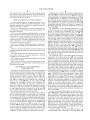
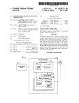
LOSLYEM
TARGET SYSTEM
SYSTEM
MEMORY
106
404
r
/
102
PROCESSOR
CORE
DEBUG
/
PORT
108”
SOFTWARE
US 6,314,530 B1
Page 2
US. PATENT DOCUMENTS
6,041,406
4,462,077
7/1984 York ................................... .. 364/300
4,598,364
7/1986
Gum e161.
714/39
371/19
5,321,828
6/1994 Phillips et al. .
5,345,580 *
9/1994 Tamaru et a1. ..................... .. 395/500
395/500
10/1994 Johnson et a1. .................... .. 395/500
?tstuma
,
,
11/1995
_
_
K5HDT,e—ma11descr1b1ngK5HDTJaH-11,1997,PP-1—6
Motorola “CPU32 Reference Manual”, pp. 7—1 thru 7—13
(admitted prior to Apr. 8, 1997).
Motorola “MEVB Quick Start Guide”, pp, 3—5 thru 7—2
(admitted prior to Apr' 8, 1997)_
a.
1,
5,446,876 * 8/1995 Levine 6161.
5,488,688
_
Revill, Geoff, “Advanced On—chip Debug for ColdFire
0 oyama e
5,469,571
OTHER PUBLICATIONS
364/300
4,611,281 * 9/1986 Suko et al.
5,058,114
10/1991 Kuboki et a1, _
5,357,626
3/2000 Mann ................................. .. 712/227
714/47
Bunnell .............................. .. 395/700
1/1996 Gonzales et al. ............... .. 395/183.1
395/183.21
~
-
]1);9";1Oper;2’_§inbedded System Engmeenng’ Apt/May
’ pp‘
'
.
.
Laws’ James R» E?iclent Program TraC1ng>8153 Computer’
5,491,793
2/1996 Somasundaram et al.
5,526,485
6/1996 Brodsky ........................ .. 395/183.14
Advanced Micro Devices, “Arn29040TM Microprocessor
User’s Manual—29K Family”, Advanced Micro Devices,
5,530,804
6/1996 Edgington et al.
5,533,192
7/1996 Hawley et al.
5,544,311
8/1996 Hafenbefg et a1~
~~ 395/18316
5,594,903
1/1997 Bunnellet a1.
..... .. 395/712
.. 395/182.07
géggs’g
5’63O’102
5/1997 Johnson et al'
""" " 395/500
Ganssle, Jack G., “Vanishing Visibility, Part 2”, Embedded
5,630,128 *
5/1997 Farrell et al.
5,615,331
.. 395/183.06
NO- 5, May 26, 1993, LOS Alamltos, CA, PP- 52—61
.... .. 395/183.04
3/1997 Tooriansetal.
5,678,003
10/1997 Brooks
*
11/1997
Funyu
........
5,724,505
3/1998 Argade et al- -
5,740,440
4/1998
West
,
,
E
b dd d S
m e
6
e
a
.
'
rogrammmg’
A
ug
_ 1997
’ pp
_
,
Tools (a Wind River Systems White paper)”, Nov. 1997, pp.
. . . . . . ..
.
P
_ 395 /183_1
712/234
-- 395/183-21
6/1998 Sites et al. ....... ..
t
Y5 ems
Systems 1:r°gramm1ng>Aug-_ 1997’ PP- 113415
T°mad°> The NFXt Generatlon of Embedded Development
. . . . . . ..
..................
ris ensen
1’
712/227
395/183.21
395/704
girlie/“Sen eta? 5,764,885
O’Farrell, Ray, “Choosing a Cross—Debugging Methodol
709/4
5,634,046 * 5/1997 Chatterjee et al.
5,642,479
6/1997 Flynn ........... ..
5,689,694
Inc. 1994, pp. 12—1 through 12—26.
1—15.
Geir, Jim, “A Kinder, Smaller Windows”, BYTE Special
Report, Aug
1997,
103_107_
Mittag, Larry, “WindoWs CE—What’s in it for You?”,
..... ..
~
.. 395/183.21
_
gingiidg‘éiléstems Programmmg’ NOV‘ 1997’ pp‘ 20 22’
5,768,152
6/1998 Battaline et al. ..
.. 364/551.01
5,771,240
6/1998 Tobin Ctal.
.... .. 371/221
OJenneS>Dan> De ugglPgwlt Rea—T1meTraCe >Em e '
5,774,708
6/1998 Klingler
395/568
@1601 Systems Programmlng, Aug- 1997,1111 5052, 54, 56,
5,802,272 *
9/1998 Sites et al. .
5,812,811
714/45
,’
,1
b
_
_ h
1
_
,,
b d
and 58
10/1998 Dubey ........................... .. 395/183.01
Levy, Markus, “WindoWs CE at the Center of a Juggling
5,828,824
10/1998 Swoboda ....................... .. 395/183.01
Act”, EDN, Jul, 17, 1997, pp, 38, 40, 42, 44, 46, and 48-49.
5,848,264
12/1998 Baird et al.
..... .. 395/500
Core, “A Real 05 for Real Time”, Sep 1996, BYTE, pp
51_52_
5,867,644
2/1999 Ranson et al. .
.. 395/183.15
5,889,981
3/1999 Betker et al. ..
395/568
Core , “A RISC OS for All Seasons” 7 DeC ' 1996 7 BYTE 7
2:38:32? i 311333 22136;; """ "
11:: 332283
4950;, f
5,903,718
579437498
5,953,530
395/183.14
395/7O4
395/704
Core’ “In emo- one HOtOS ’Jun-199Z>BYTE’PP- 3‘ 4
Core, A New EpOCh for Hand—Helds , OCt. 1997, BYTE,
1111-4546
11/1999 Mann .......... ..
11/1999 Miyamori et a1. .
712/227
714/45
IBM Technical Disclosure Bulletin, “Trace Array”, Vol. 35,
NO_ 2, pp Ju1_ 1992, 138—140_
5,996,092
11/1999 Augsburg et a1. .
714/38
6,009,270
12/1999 Mann ................................. .. 395/704
5,978,902
5,978,937
5/1999 Marik ....... ..
8/1999 Yano et a1
9/1999 Rishi et a1
_
* cited by examiner
,,
pp'
5 5
U.S. Patent
i
Nov. 6, 2001
Sheet 1 0f 8
US 6,314,530 B1
5E051
8T (2:
K
25% E8
N25we
58
\
\
5%,:
52:;%5o%
5;
.wE
M
U.S. Patent
Nov. 6, 2001
Sheet 3 0f 8
H>:m25low 5H>7235 m>:65l<ow
mo l
58
US 6,314,530 B1
.wE
m
U.S. Patent
20
Nov. 6, 2001
Sheet 5 0f 8
US 6,314,530 B1
15
0
O OIOIOIlBBIBZIBlIlIOIOIOIOIOIOIOIOIOIOIOIO
TCODEIl
Only 5-bits of BFIELD used
FIG. 6A
20 l9
15
O
O
ITCODIE=2I
I
ITADQR_HI, high l6I—bitIs ofIElP Itorggt logicolIuddfessI
O
ITCODIE=7I
I
ITADIDR_LI, lovIi l6I—bitsI of IEIP tIcrgeIt logical Iuddrfess I
FIG. 6B
20 l9
l5
0
O
ITCODIE=8I
ITADDIR_HI higIh l6I—bitsI of IEIP IstopIinstrIucticIm loIgicolI oddIressI
O
ITCODIE=7I
ITADIIJR_LI, lovi l6—IbitsI of EIP sItop IinstrpctioIn logical IuddrIess I
O
ITCODIE=4I
IBADIDR_IH, hiIgh lI6—biIts oIf CurIrentI seginentI bosIe odIdresIs
O
ITCODIE=7I
BAQDR_IL, loIw bils lf?—4 Iof sggmeInt bpse IoddnIess — PG SZ F/P
FIG. 6C
20 l9
l5
0
V
ITCODIE=lI
lI
I
O
O
O
ITC0DIE=6I
ITCODIE=7I
lCODIE=3I
TADIIJR_HI, high l6I—bitIs of IElP for iriterrqptedI instIructiIon IqgicolI uddIress
TADIDR_LI, lovIi l6I—bitsI of EIP fIor inIterruIptedI instIructiIon lqgicolI oddIress
IBADDIR_HI higIh l6I—bit§ of Iprevious IsegnIientIbosq 0d<IlressI
ITCODIE=7I
BAQDR_IL, loIw biIts 15-4 Iof seIrgmeInt bIose IoddnIess — PG SZ R/P
I
I
I
I
I
I
I
IBFIEILDI
IvectIor nIumbgr
I
I
I
I
I
I
I
O
ITCODIE=5I
I
I
O
ITCODIE=7I
ITAD|I)R_ll, high lbI—bitIs ofIinteIrruptI honIdlerIlogicIol ogldresIs
O
ITCODIE=7I
I
ITADDIR_L,I lowI16—Ibits Iof iqstrugtionI logiIcol qddreIss I
FIG. 6D
I
I
U.S. Patent
Nov. 6, 2001
Sheet 7 0f 8
US 6,314,530 B1
711
§
APPLICATIONS
715
717
S
REMOTE APl
SHELLS
M
713S
OBJECT
STORES
COMMON
CONTROLS
SERV'CES
705
0
J
S
V
KERNEL
707“
COMMUNICATIONS
Graphic
Windowing Ond
Event Subs stem
8
(GWES?
70‘
CORE OS
Device Drivers
OEM ABSTRACTION LAYER
S
S
703
709
Hardware
FIG. 7
U.S. Patent
Nov. 6, 2001
US 6,314,530 B1
Sheet 8 0f 8
TASK 1 MEMORY
Thread 1 “V 807
OS MEMORY
w 803
Thread 1
Thread n
Thread 2
TASK N MEMORY
Thread 1
Thread n
w 805
Thread n
OS
APPLICATION TASKS
FIG. 8
US 6,314,530 B1
1
2
PROCESSOR HAVING A TRACE ACCESS
INSTRUCTION TO ACCESS ON-CHIP
TRACE MEMORY
sor complexity, higher clock speeds, use of on-chip instruc
tion and data cache and packaging problems have reduced
the availability of ICE. All to often it is quite some time after
a processor’s introduction before an ICE becomes available,
RELATED APPLICATIONS
and only then if the processor is Widely accepted.
In-circuit emulators do provide certain advantages over
This application claims priority to US. application Ser.
No. 60/043,070, ?led Apr. 8, 1997, Which is hereby incor
other debug environments by offering complete control and
porated by reference.
visibility over memory and register contents, as Well as
overlay and trace memory in case system memory is insuf
?cient. Use of traditional in-circuit emulators, Which
BACKGROUND OF THE INVENTION
involves interfacing a custom emulator back-end With a
processor socket to alloW communication betWeen emula
1. Field of the Invention
The invention relates to debug support in operating
systems, and more particularly to an operating system pro
viding on-chip trace support.
15
2. Description of the Related Art
tion equipment and the target system, is becoming increas
ingly dif?cult and expensive in today’s age of exotic pack
ages and slinking product life cycles.
Assuming full-function in-circuit emulation is required,
The availability of greater integration, loWer costs, higher
performance and product innovation has fueled rapid expan
there are several knoWn processor manufacturing techniques
able to offer the required support for emulation equipment.
sion of products based on embedded microprocessors. At the
Most processors intended for personal computer (PC) sys
tems utiliZe a multiplexed approach in Which existing pins
same time, the groWth in softWare complexity, coupled With
the increasing processor clock speeds, has placed an increas
ing burden on application softWare developers. The cost of
developing and debugging neW softWare products is noW a
signi?cant factor in processor selection. In response, a tools
industry has evolved to provide a range of often incompat
ible tools to satisfy hardWare and softWare development
25
are multiplexed for use in softWare debug. This approach is
not particularly desirable in the embedded industry, Where it
is more dif?cult to overload pin functionality.
Other more advanced processors multiplex debug pins in
time. In such processors, the address bus is used to report
softWare trace information during a BTA-(Branch Target
requirements.
Address) cycle. The BTA-cycle, hoWever, must be stolen
from the regular bus operation. In debug environments
A processor’s failure to adequately facilitate softWare
debug results in longer customer development times and
Where branch activity is high and cache hit rates are loW, it
reduces the processor’s attractiveness for use Within indus
becomes impossible to hide the BTA-cycles. The resulting
try. The need to provide softWare debug support is particu
larly acute Within the embedded microprocessor industry,
Where specialiZed on-chip circuitry is often combined With
con?ict over access to the address bus necessitates processor
“throttle back” to prevent loss of instruction trace informa
a processor core.
In addition to the softWare engineer, other parties are also
35
tion. In the communications industry, for example, softWare
typically makes extensive use of branching and suffers poor
cache utiliZation, often resulting in 20% throttle back or
affected by the type and availability of debug tools or
involved in their development. These parties include: the
“trace” algorithm developer Who must search through cap
amount for embedded products Which must accommodate
real-time constraints.
tured softWare trace data that re?ects instruction execution
How in a processor; the in-circuit emulator hardWare devel
In another approach, a second “trace” or “slave” processor
is combined With the main processor, With the tWo proces
more. That amount of throttle back is an unacceptable
oper Who deals With problems of signal synchroniZation,
sors operating in-step. Only the main processor is required
clock frequency and trace bandWidth; and the processor
to fetch instructions. The second, slave processor is used to
monitor the fetched instructions on the data bus and keeps its
internal state in synchroniZation With the main processor.
The address bus of the slave processor functions to provide
trace information. After poWer-up, via a JTAG (Joint Test
manufacturer Who does not Want a solution that results in
increased processor cost or design and development com
plexity.
45
With desktop systems, complex multitasking operating
systems are currently available to support debugging.
HoWever, the initial task of getting these operating systems
Action Group) input, the second processor is sWitched into
running reliably often requires special development equip
instructions, its address bus and other pins provide the
ment. While not the standard in the desktop environment, the
use of such equipment is often the approach taken Within the
necessary trace information.
embedded industry.
Traditionally, the most poWerful piece of debug equip
port into every processor, but only bonding-out the neces
sary signal pins to support e.g., trace capability, in a limited
a slave mode of operation. Free from the need to fetch
Another existing approach involves building debug sup
ment available to an embedded project has been the 55 number of packages. These specially packaged versions of
the processor are used during debug and replaced With the
smaller package for ?nal production. That bond-out
approach suffers from the need to support additional bond
in-circuit emulator (ICE). They are most frequently (but not
exclusively) used during the early stages of “bringing up the
hardWare”. In many cases ICE equipment is too expensive
to be Widely available to all project members. In fact
pad sites in all fabricated devices. That can be a burden in
typically only softWare engineers Which are someWhat
hardWare-friendly have the necessary skills required to drive
small packages and pad limited designs, particularly if a
substantial number of extra pins are required by the debug
an ICE.
support variant. Additionally, the debug capability of the
specially packaged processors is unavailable in typical
The availability of an ICE gives project engineers the
con?dence that they can rapidly resolve any difficult devel
opment problem they encounter. For this reason, many
processor-based production systems.
project teams insist that an ICE be available or they may
The rising cost of ICE and the increase in its unavailabil
ity has lead to a search for alternatives. The use of general
select an alternative processor. Unfortunately, rising proces
purpose logic analyZers, With support softWare, has provided
65
US 6,314,530 B1
3
4
one alternative. However, these tool combinations are gen
to application debug. The limitations of the existing solu
erally considered even harder to drive than ICE. The primary
reason engineers select an ICE solution is because of its
program trace capability. The trace capability of a logic
processor clock frequencies continue to increase, softWare
complexity continues to groW and expensive ICE solutions
analyZer is the reason engineers resort to their use When an
become more and more prohibitive.
tions are likely to be exacerbated in the future as internal
ICE is unavailable.
SUMMARY OF THE INVENTION
In yet another debug approach (the “Background Debug
Mode” by Motorola, Inc.) limited on-chip debug circuitry is
provided for basic run control. Through a dedicated serial
link requiring additional pins, this approach alloWs a debug
10
ger to start and stop the target system and apply basic code
Accordingly, the invention provides a method of operat
ing a computer system that includes a memory for storing
instructions executable by a processor. The method includes
breakpoints by inserting special instructions in system
executing a trace access instruction stored in the memory to
access an on-chip trace memory on the processor. The trace
memory. Once halted, special commands are used to inspect
memory variables and register contents.
Typically a project engineer Will utiliZe a ROM monitor
memory has a plurality of locations for storing trace infor
mation that indicates execution How of a plurality of instruc
15
When an ICE solution is too expensive or unavailable. These
tions in the processor. The trace access instruction can be a
Write instruction or a read instruction. Typically, both read
and Write to the trace memory is provided. The method
further provides the capability to trace on execution of an
monitors consist of relatively small programs Which are
located in the target system’s ROM or Flash memory. They
also typically have a small RAM requirement The monitor
executable thread by providing to the processor an indica
program supports control and visibility into the program’s
tion to trace on execution of an executable thread. That
register and memory contents, but no trace of program
execution. Often projects Will be supported With one or tWo
indicates to the processor to provide trace information When
the executable thread executes. When execution of the
executable thread starts the; processor places an identi?er
corresponding to the executable thread into the trace
ICEs, With the rest of the softWare engineers Working With
a target monitor.
An additional tool available to the embedded project is the
25
memory to indicate that subsequent entries placed into the
trace memory are part of the executable thread. The proces
sor may also provide an entry indicating When the thread
ROM emulator. This enables system ROM or RAM to be
replaced With a dual ported memory Which can be accessed
by both the target and host processors. The use of a ROM
stops executing.
emulator does provide for fast data and program transfer,
In still another embodiment, the method provides storing
Which is the primary reason for its selection.
The loW cost of ROM monitors make them popular, but
their use has several draWbacks: They require ROM and
RAM resources to be reserved Within the target systems
data in the trace memory prior to the access instruction
memory. They require an on-chip or off-chip peripheral,
such as a Universal Asynchronous Receiver Transmitter
according to the privilege level of the code being executed.
When an application task is executing With a ?rst privilege
level, trace information is loaded into the trace memory.
35
(UART), to support communication With the controlling
When a task starts to execute With a different privilege level,
eg a system task, the processor stops providing trace
(host) platform. Subsequent updating of the monitor pro
information to the trace memory.
Another embodiment of the invention provides a com
gram is often an arduous process.
puter program embodied on computer readable media, for
execution on a computer system including a processor, the
processor including an on-chip trace memory, and a memory
In recent years there has been greater use of sophisticated
tools such as multitasking operating systems, library
resources and source-level debuggers, to name only a feW.
for storing instructions executable by the processor. The
As discussed, complex multi-tasking operating systems are
currently available to support debugging With desktop sys
computer program includes a trace access instruction for
accessing the trace memory on the processor Which has a
tems. In general, tools for use With PC softWare develop
ment have reached a high level of functionality and sim
plicity of use. That has not gone unnoticed by engineers in
45
plurality of locations for storing trace information indicative
of instruction execution How in the processor. The trace
access instruction may be a Write or read.
the embedded industry, and there is noW a demand for a
In another embodiment of the invention, a method is
provided for operating a computer system that includes a
processor and a memory storing instructions for the proces
similar level of tool capability.
Several studies have shoWn that presently only about 50%
operating systems although this number is groWing. One
sor. The method includes identifying an executable thread to
trace as a ?rst trace condition. In response to the identifying
deterrent to use of multitasking operating systems has cer
step, an indicator is stored that the executable thread is to be
of 32-bit embedded systems make use of a multitasking
tainly been cost, but more important has been the perceived
complexities of getting the system running. Often there are
dif?cult tool transitions required as debugging proceeds
from kernel-mode to application-mode debug. There is also
55
traced. Additional trace information is provided indicating
When to enable tracing instruction execution ?oW Within the
executable thread. The additional trace information is a
second trace condition. Trace information is provided When
the burden of often having to ?rst get a ROM monitor
the ?rst and second trace conditions are both true.
running before commencing kernel and driver con?guration
for the particular system.
In another embodiment of the invention, an operating
system includes a trace handling component. The operating
Thus, the current solutions for softWare debugging suffer
from a variety of limitations, including: increased packaging
and development costs, circuit complexity and processor
throttle back. Further, there is currently no adequate loW
cost procedure for providing trace information. Also, debug
system is for execution on a computer system that includes
a processor and memory for storing instructions executable
by the processor. The trace handling component includes a
trace read instruction for accessing an on-chip trace memory
on the processor. The trace read instruction is stored in the
instruction memory. The trace memory has a plurality of
locations for storing trace information indicative of instruc
ging embedded applications utiliZing multi-tasking operat
ing systems can result in difficult tool transitions from kernel
65
US 6,314,530 B1
5
6
tion execution How in the processor. The operating system
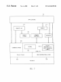
Referring noW to FIG. 2, details of an embedded proces
sor device 102 according to the present invention are pro
vided. In addition to the processor core 104, FIG. 2 depicts
various elements of an enhanced embodiment of the debug
also includes a trace Write instruction. The Write instruction
Writes data identi?ed by the trace Write instruction to one of
the locations in the trace memory.
port 100 capable of utiliZing and controlling the trace
BRIEF DESCRIPTION OF THE DRAWINGS
memory (also referred to herein as trace cache) 200. Many
other con?gurations are possible, as Will become apparent to
those skilled in the art, and the various processor device 102
A better understanding of the present invention can be
obtained When the following detailed description of the
preferred embodiment is considered in conjunction With the
components described beloW are shoWn for purposes of
illustrating the bene?ts associated With providing an on-chip
folloWing draWings, in Which:
trace cache 200.
FIG. 1 is a block diagram of a softWare debug environ
ment utiliZing a softWare debug solution in accordance With
Of signi?cance to the disclosed embodiment of the
invention, the trace control circuitry 218 and trace cache 200
operate to provide trace information for reconstructing
the present invention;
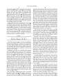
FIG. 2 is a block diagram providing details of an exem
plary embedded processor product incorporating an on-chip
instruction execution How in the processor core 104. The
15
trace control circuitry 218 supports “tracing” to a trace pad
interface port 220 or to the instruction trace cache 200 and
instruction trace cache according to the present invention;
FIG. 3 is a simpli?ed block diagram depicting the rela
tionship betWeen an exemplary instruction trace cache and
other components of an embedded processor product
provides user control for selectively activating instruction
trace capture. Other features enabled by the trace control
circuitry 218 include programnability of synchroniZation
address generation and user speci?ed trace records, as
discussed in greater detail beloW. The trace control circuitry
218 also controls a trace pad interface port 220. When
utiliZed, the trace pad interface port 220 is capable of
according to the present invention;
FIG. 4 is a ?oWchart illustrating softWare debug com
mand passing according to one embodiment of the inven
providing trace data While the processor core 104 is execut
tion;
FIG. 5 is a ?oWchart illustrating enhanced softWare port
command passing according to a second embodiment of the
25
ing instructions, although clock synchroniZation and other
issues may arise. The instruction trace cache 200 addresses
invention;
many of these issues, improving bandWidth matching and
alleviating the need to incorporate throttle-back circuitry in
FIGS. 6A—6G illustrate the general format of a variety of
trace cache entries for reporting instruction execution
the processor core 104.
according to the invention; and
FIG. 7 shoWs an operating system con?gurable according
At a minimum, only the conventional JTAG pins need be
supported in the softWare debug port 100 in the described
embodiment of the invention. The JTAG pins essentially
to the present invention.
FIG. 8 shoWs allocation of memory betWeen the OS and
become a transportation mechanism, using existing pins, to
application tasks in a multi-tasking, multi-threaded operat
enter commands to be performed by the processor core 104.
35
ing system environment.
DESCRIPTION OF THE PREFERRED
Test Access Port (TAP) controller 204 are conventional
JTAG support signals and knoWn to those skilled in the art.
EMBODIMENT(S)
Turning noW to the draWings, FIG. 1 depicts an exemplary
softWare debug environment illustrating a contemplated use
of the present invention. A target system T is shoWn con
taining an embedded processor device 102 according to the
present invention coupled to system memory 106. The
embedded processor device 102 incorporates a processor
More speci?cally, the test clock signal TCK, the test mode
select signal TMS, the test data input signal TDI and the test
data output signal TDO provided to and driven by the JTAG
As discussed in more detail beloW, an “enhanced” embodi
ment of the debug port 100 adds the command acknoWledge
signal CMDACK, the break request/trace capture signal
BRTC, the stop transmit signal STOPTX, and the trigger
signal TRIG to the standard JTAG interface. The additional
45
core 104, an instruction trace memory (also referred to
signals alloW for pinpoint accuracy of external breakpoint
assertion and monitoring, triggering of external devices in
response to internal breakpoints, and elimination of status
polling of the JTAG serial interface. These “sideband”
herein as trace cache 200) (FIG. 2), and a debug port 100.
Although not considered critical to the invention, the
embedded processor 102 may incorporate additional cir
functions, or may take the form of a stand-alone processor
signals offer extra functionality and improve communica
tions speeds for the debug port 100. These signals also aid
in the operation of an optional parallel port 214 provided on
or digital signal processor. Preferably, the debug port 100
special bond-out versions of the disclosed embedded pro
uses an IEEE-1149.1-1990 compliant JTAG interface or
cessor device 102.
cuitry (not shoWn) for performing application speci?c
other similar standardiZed serial port interface.
Ahost system H is used to execute debug control softWare
55
When a DEBUG instruction has been Written to the JTAG
112 for transferring high-level commands and controlling
the extraction and analysis of debug information generated
by the target system T. The host system H and target system
instruction register, a serial debug shifter 212 is connected to
the JTAG test data input signal TDI and test data output
signal TDO, such that commands and data can then be
loaded into and read from debug registers 210. In the
T of the disclosed embodiment of the invention communi
cate via a serial link 110. Most computers are equipped With
a serial or parallel interface Which can be inexpensively
connected to the debug port 100 by means of a serial
connector 108, alloWing a variety of computers to function
as a host system H. Alternatively, the serial connector 108
could be replaced With higher speed JTAG-to-netWork con
version equipment. Further, the target system T can be
con?gured to analyZe debug/trace information internally.
Via the conventional JTAG signals, the JTAG TAP con
troller 204 accepts standard JTAG serial data and control.
65
disclosed embodiment of the invention, the debug registers
210 include tWo debug registers for transmitting (TXi
DATA register) and receiving (RXiDATA register) data, an
instruction trace con?guration register (ITCR), and a debug
control status register (DCSR).
A control interface state machine 206 coordinates the
loading/reading of data to/from the serial debug shifter 212
US 6,314,530 B1
7
8
and the debug registers 210. A command decode and pro
cessing block 208 decodes commands/data and dispatches
them to processor interface logic 202 and trace debug
interface logic 216. In addition to performing other
functions, the trace debug interface logic 216 and trace
control logic 218 coordinate the communication of trace
command pending ?ag set and desired data (if applicable,
otherWise Zero) in the data ?eld. Control proceeds to step
406 Where the pending command is loaded/unloaded and the
command ?nished ?ag checked. Completion of a command
typically involves transferring a value betWeen a data reg
ister and a processor register or memory/IO location. After
the command has been completed, the processor 104 clears
information from the trace cache 200 to the TAP controller
204. The processor interface logic 202 communicates
the command pending ?ag and sets the command ?nished
directly With the processor core 104, as Well as the trace
control logic 218. As described more fully beloW, parallel
port logic 214 communicates With a control interface state
10
machine 206 and the debug registers 210 to perform parallel
data read/Write operations in optional bond-out versions of
?ags. If the pending ?ag is reset to Zero and the ?nished ?ag
is set to one, the previous command has ?nished. The status
the embedded processor device 102.
Before debug information is communicated via the debug
port 100 using only conventional J TAG signals, the port 100
is enabled by Writing the public JTAG instruction DEBUG
?ag, at the same time storing a value in the data ?eld if
applicable. The entire 38-bit register is shifted out to the host
to monitor the command ?nished and command pending
15
into a JTAG instruction register contained Within the TAP
of the ?ags is captured by the control interface state machine
206. A slave copy of the ?ags’ status is saved internally to
determine if the next instruction should be loaded. The slave
copy is maintained due to the possibility of a change in ?ag
status betWeen TAP controller 204 states. This alloWs the
controller 204. As in Table 1, the JTAG instruction register
of the disclosed embodiment is a 38-bit register comprising
processor 104 to determine if the previous instruction has
?nished before loading the next instruction.
If the ?nished ?ag is not set as determined in step 408,
a 32-bit data ?eld (debugidata{31:0}), a four-bit command
?eld to point to various internal registers and functions
control proceeds to step 410 and the loading/unloading of
the 38-bit command is repeated. The command ?nished ?ag
provided by the debug port 100, a command pending ?ag,
and a command ?nished ?ag. It is possible for some com
is also checked. Control then returns to step 408. If the
mands to use bits from the debugidata ?eld as a sub?eld to 25
?nished ?ag is set as determined in step 408, control returns
extend the number of available commands.
to step 406 for processing of the next command. DEBUG
mode is exited via a typical JTAG process.
TABLE 1
37
5
debug_data
Command
Returning to FIG. 2, the aforementioned optional side
2
1
band signals are utiliZed in the enhanced debug port 100 to
O
provide extra functionality. The optional sideband signals
IP IF I
include a break request/trace capture signal BRTC that can
function as a break request signal or a trace capture enable
signal depending on the status of bit set in the debug
This JTAG instruction register is selected by toggling the
test mode select signal TMS. The test mode select signal
TMS alloWs the JTAG path of clocking to be changed in the
35
scan path, enabling multiple paths of varying lengths to be
request/trace capture signal BRTC enables trace capture.
Deasserting the signal turns trace capture off. The signal
speci?ed system registers.
Referring noW to FIG. 3, a simpli?ed block diagram
takes effect on the next instruction boundary after it is
depicting the relationship betWeen an exemplary instruction
trace cache 200 and other components of an embedded
45
asserted at any time.
The trigger signal TRIG is con?gured to pulse Whenever
Increasing the siZe of the trace cache 200 increases the
amount of instruction trace information that can be captured,
although the amount of required silicon area may increase.
As described in more detail beloW, the trace cache 200 of
the disclosed embodiment of the invention stores a plurality
of 20-bit (or more) trace entries indicative of the order in
Which instructions are executed by the processor core 104. 55
Other information, such as task identi?ers and trace capture
stop/start information, can also be placed in the trace cache
200. The contents of the trace cache 200 are provided to
the 38-bit serial value is shifted in as a Whole, With the
detected and is synchroniZed With the internal processor
clock. The break request/trace capture signal BRTC may be
an internal processor breakpoint has been asserted. The
trigger signal TRIG may be used to trigger an external
circular cache that records the most recent trace entries.
external hardWare, such as the host system H, via either
serial or parallel trace pins 230. Alternatively, the target
system T can be con?gured to examine the contents of the
trace cache 200 internally.
FIG. 4 provides a high-level ?oW chart of command
passing When using a standard JTAG interface. Upon enter
ing debug mode in step 400 the DEBUG instruction is
Written to the TAP controller 204 in step 402. Next, step 404,
signal BRTC is set to function as a break request signal, it
is asserted to cause the processor 104 to enter debug mode
(the processor 104 can also be stopped by scanning in a halt
command via the convention JTAG signals). If set to func
tion as a trace capture enable signal, asserting the break
used. Preferably, the JTAG instruction register is accessible
via a short path. This register is con?gured to include a soft
register for holding values to be loaded into or received from
processor device 102 according to the present invention is
shoWn. In one contemplated embodiment of the invention,
the trace cache 200 is a 128 entry ?rst-in, ?rst-out (FIFO)
control/status register. If the break request/trace capture
capturing device such as a logic analyZer, and is synchro
niZed With the trace record capture clock signal TRACE
CLK. When a breakpoint is generated, the event is synchro
niZed With the trace capture clock signal TRACECLK, after
Which the trigger signal TRIG is held active for the duration
of trace capture.
The stop transmit signal STOPTX is asserted When the
processor 104 has entered DEBUG mode and is ready for
register interrogation/modi?cation, memory or I/O reads and
Writes through the debug port 100. In the disclosed embodi
ment of the invention, the stop transmit signal STOPTX
re?ects the state of a bit in the debug control status register
(DCSR). The stop transmit signal STOPTX is synchronous
With the trace capture clock signal TRACECLK.
65
The command acknoWledge signal CMDACK is
described in conjunction With FIG. 5, Which shoWs simpli
?ed command passing in the enhanced debug port 100 of
FIG. 2. Again, to place the target system T into DEBUG
US 6,314,530 B1
9
10
mode, a DEBUG instruction is written to the TAP controller
204 in step 502. Control proceeds to step 504 and the
TABLE 2-continued
command acknowledge signal CMDACK is monitored by
the host system H to determine command completion status.
BIT
SYMBOL
DESCRIPTION/FUNCTION
This signal is asserted high by the target system T simulta
neously with the command ?nished ?ag and remains high
until the next shift cycle begins. When using the command
3
ITM
Sets internal or external (bond-out)
instruction tracing
mode. In internal trace con?guration,
the trace buffer
behaves as a circular buffer; in
external trace mode the
trace records are continuously sent
acknowledge signal CMDACK, it is not necessary to shift
out the JTAG instruction register to capture the command
?nished ?ag status. The command acknowledge signal
CMDACK transitions high on the next rising edge of the test
clock signal TCK after the command ?nished ?ag has
changed from Zero to one. When using the enhanced JTAG
signals, a new shift sequence (step 506) is not started by the
host system H until the command acknowledge signal
CMDACK pin has been asserted high. The command
acknowledge signal CMDACK is synchronous with the test
1O
out through the parallel
2
1
TINIT
TRIGEN
trace port 220 while the core executing
Trace initialization
Enables pulsing of external trigger
signal TRIG following
receipt of any legacy debug breakpoint;
15
O
GTEN
independent of the
Debug Trap Enable function in the DCSR
Global enable for instruction tracing
through the internal
clock signal TCK. The test clock signal TCK need not be
trace buffer or via the external
clocked at all times, but is ideally clocked continuously
when waiting for a command acknowledge signal
(bond-out) interface
CMDACK response.
Another debug register, the debug control/status register
Also included in debug register block 210 is an instruction
trace con?guration register (ITCR) shown in Table 2. This
32-bit register provides for the enabling/disabling and con
?guration of instruction trace debug functions. Numerous
such functions are contemplated, including various levels of
tracing, trace synchroniZation force counts, trace
initialiZation, instruction tracing modes, clock divider ratio
25
(DCSR) shown in Table 3, provides an indication of when
the processor 104 has entered debug mode and allows the
processor 104 to be forced into DEBUG mode through the
enhanced JTAG interface. As shown in the following table,
the DCSR also enables miscellaneous control features, such
as: forcing a ready signal to the processor 104, controlling
memory access space for accesses initiated through the
information, as well as additional functions shown in the
debug port, disabling cache ?ush on entry to the DEBUG
following table. The ITCR is accessed through a JTAG
mode, the TX and RX bits, the parallel port 214 enable,
forced breaks, forced global reset, and other functions. The
ordering or presence of the various bits in either the ITCR
instruction register write/read command as is the case with
the other registers of the debug register block 210, or via a
reserved instruction.
35
or DCSR is not considered critical to the operation of the
invention.
TABLE 2
TABLE 3
EH‘
SYMBOL
DESCRIPTION/FUNCT ION
31:30
29
28
27
Reserved
RXINTEN
TXINTEN
TX
Reserved
Enables interrupt when RX bit is set
Enables interrupt when TX bit is set
Indicates that the target system T is
ready to transmit data
to the host system H and the data is
available in the
BIT
RX
DESCRIPTION/FUNCTION
Reserved
Indicates that the target system T
is ready to transmit data
to the host system H and the data is available in the
TXLDATA register
10
RX
9
8
DISFLUSH
SMMSP
45
TXiDATA register
26
SYMBOL
31:12 Reserved
11
TX
Indicates that data has been
received from the host and
placed in the RXiDATA register
Indicates that data has been received
from the host and
placed in the RXLDATA register
Disables cache ?ush on entry to DEBUG mode
Controls memory access space
25
24
DISL1TR
DISLOTR
Disables level 1 tracing
Disables level 0 tracing
system management mode memory) for
23
DISCSB
Disables current segment base trace record
accesses initiated
22:16 TSYNC{6:O}
(normal memory space/
through the Debug Port 100
Sets the maximum number of
Branch Sequence trace
records that may be output by the
7
STOP
Indicates whether the processor
104 is in DEBUG mode
6
FRCRDY
Forces the ready signal RDY to the
(equivalent to stop transmit signal STOPTX
trace control block 218
before a synchronizing address record is forced
15
TSR3
Bits 15:8 allow the user to map four
processor 104 to be
55
breakpoint register as
trace control breakpoints.
or
or
or
or
clears
clears
clears
clears
14
13
12
TSR2
TSR1
TSRO
11
1O
9
8
TRACE3
TRACE2
TRACE1
TRACEO
Enables
Enables
Enables
Enables
7
TRON
Trace on/off
6:4
TCLK{2:O}
Encoded divider ratio between
Trace
Trace
Trace
Trace
trace
trace
trace
trace
mode
mode
mode
mode
pulsed for one processor clock;
useful when it is apparent
Sets
Sets
Sets
Sets
mode
mode
mode
mode
on
on
on
on
toggling
toggling
toggling
toggling
internal processor clock
and TRACECLK
DR3
DR2
DR1
DRO
that the processor 104 is stalled
trap
trap
trap
trap
using
using
using
using
waiting for a ready signal
5
BRKMODE
from a non-responding device
Selects the function of the break
request/trace capture
DR3
DR2
DR1
DRO
signal BRTC (break request or
trace capture on/off)
4
DBTEN
Enables entry to debug mode or
toggle trace mode enable
on a trap/fault via processor 104
65
registers DRO-DR7 or
other legacy debug trap/fault mechanisms
US 6,314,530 B1
11
12
This technique enables an operating system or application
to communicate With the host system H Without stopping
processor 104 execution. Communication is conveniently
achieved via the debug port 100 With minimal impact to
TABLE 3-continued
BIT
SYMBOL
DESCRIPTION/FUNCTION
3
2
PARENB
DSPC
Enables parallel port 214
Disables stopping of internal processor
1
FBRK
clocks in the Halt
and Stop Grant states
Forces processor 104 into DBBUG mode at the next
the communication link is driven in a polled mode.
instruction boundary (equivalent to
pulsing the external
BRTC pin)
0
FRESET
on-chip application resources. In some cases it is necessary
to disable system interrupts. This requires that the RX and
TX bits be examined by the processor 100. In this situation,
10
Forces global reset
When in cross debug environment such as that of FIG. 1,
it is necessary for the parent task running on the target
system T to send information to the host platform H con
trolling it. This data may consist, for example, of a character
stream from a prinif( ) call or register information from a
Some embedded systems require instruction trace to be
examined While maintaining I/O and data processing opera
tions. Abond-out version of the embedded processor device
102 may therefore be preferable to provide the trace data.
15
Thus, in the disclosed embodiment of the invention, an
optional bond-out version of the embedded processor device
102 is provided in Which a communication port is provided
that can be selected as a parallel debug port or a trace port.
The parallel debug port is a high performance port 214
Task’s Control Block (TCB). One contemplated method for
transferring the data is for the operating system to place the
Which physically shares a substantial number of the bond
out pads utilized by the instruction trace port 220. The trace
data in a knoWn region, then via a trap instruction, cause
DEBUG mode to be entered.
port 220 provides external trace capability While the parallel
debug port 214 provides parallel command and data access
to the debug port 100. The input/output terminals of the
Via debug port 100 commands, the host system H can
bond-out port are shoWn in Table 4. Some of the pins of the
then determine the reason that DEBUG mode Was entered,
and respond by retrieving the data from the reserved region.
25
However, While the processor 104 is in DEBUG mode,
normal processor execution is stopped. As noted above, this
is undesirable for many real-time systems.
This situation is addressed according to the present inven
bond-out port are exclusive to the parallel port, some are
exclusive to the trace port and the remainder shared. In the
embodiment shoWn, 20 bits are shared (PDATA, PADR and
PRW). When the port is selected as a debug port, the TCK
is used to synchronize all data transactions. TCK should be
tion by providing tWo debug registers in the debug port 100
continually clocked When the parallel debug interface is
for transmitting (DXiDATA register) and receiving (RXi
enabled. When the port is selected as a trace port, the
DATA register) data. These registers can be accessed using
the soft address and JTAG instruction register commands.
As noted, after the host system H has Written a debug
instruction to the JTAG instruction register, the serial debug
shifter 212 is coupled to the test data input signal TDI line
and test data output signal TDO line.
TRACECLK is provided to synchronize the output data.
35
The parallel port 214 provides a 16-bit Wide bidirectional
data bus (PDATA{15:0}), a 3-bit address bus (PADR{2:0}),
a parallel debug port read/Write select signal (PRW). In
When the processor 104 executes code causing it to
transmit data, it ?rst tests a TX bit in the ITCR. If the TX bit
addition the bond out port includes a trace valid signal TV
and an instruction trace record output clock TRACECLK
utilized When the port is being used as a trace port. Although
not shared With the trace interface port 220, a parallel bus
is set to zero then the processor 104 executes a processor
request/grant signal pair PBREQ/PBGNT are also provided.
instruction (either a memory or I/ O Write) to transfer the data
to the TXiDATA register. The debug port 100 sets the TX
bit in the DCSR and ITCR, indicating to the host system H
that it is ready to transmit data. Also, the STOPTX pin is set
high. After the host system H completes reading the transmit
TABLE 4
45 Name
data from the TXiDATA register, the TX bit is set to zero.
ATXINTEN bit in the ITCR is then set to generate a signal
TRACECLK
Resis-
Sync
I/O
tor
Clock
Output
—
—
output clock
TV
only When the TX bit in the ITCR transitions to zero. When
the TXINTEN bit is not set, the processor 104 polls the
Output
PD
TRACECLK O = Valid trace
record, 1 =
no trace record
This pin not shared
ITCR to determine the status of the TX bit to further transmit
data.
When the host system H desires to send data, it ?rst tests
With parallel bus
interface
PDATA[15:O]
Bidi
PD
TCK/
path. Shared With pins
system H Writes the data to the RXiDATA register and the
TBUS[15:O]
RX bit is set to one in both the DCSR and ITCR. A RXINT
PADR[2:O]
Bidi
PD
bit is then set in the ITCR to generate a signal to interrupt
TCK/
Parallel debug port
TRACECLK address. Shared
With pins
the processor 104. This interrupt is only generated When the
TBUS[18:16]
RX in the ITCR transitions to one. When the RXINTEN bit
PRW
is not set, the processor 104 polls the ITCR to verify the
status of the RX bit. If the RX bit is set to one, the processor
instruction is executed to read data from the RXiDATA
Bidi
PD
TCK/
Parallel debug port
TRACECLK read/Write select.
Shared With
TBUS[19] pin
1 = Perform a parallel
register. After the data is read by the processor 104 from the
status of the RX bit to further send data.
Parallel debug
TRACECLK port data
a RX bit in the ITCR. If the RX bit is set to zero, the host 55
system H continuously reads the ITCR to determine the
Instruction
Trace record
to interrupt the processor 104. The interrupt is generated
RXiDATA register the RX bit is set to zero. The host
Description
read from the
65
serial debug register
0 = Perform a parallel
US 6,314,530 B1
Name
I/O
PBREQ
13
14
TABLE 4-continued
TABLE S-continued
Resis-
Sync
tor
Clock
Output
Command
TCK
Description
5
Code
De?nition
Write to the
0010
general register read
serial debug register
0011
1 = Request
Host to
enable parallel
bus interface
0 = Request
Host to
general register Write
0100
0101
0110
10 0111
Serial/parallel Debug register read
Serial/parallel Debug register Write
reserved
Misc. Serial/parallel Debug functions per debugidata[3:0]
0
eXit via RESET (hard reset)
1
eXit via SRESET (soft reset)
disable parallel
PBGNT
Input
PD
2
bus interface
This pin not
shared With
trace bus interface
1 = Host
has enabled
TCK
Instruction step (may destroy soft address)
Bit 7 of the Debug
Control/Status register or the eXternal
STOPTX pin should be
monitored to determine When the instruction step is
completed. Unlike the TF bit, this
command Will step into
15
parallel bus
interrupts.
interface
0 = Host
2O
3
peripheral reset (CPU not reset)
4
Read trace buffer at displacement
has disabled
given in [soft address]
parallel bus
interface
This pin not shared
With trace bus
5
eXit to instruction at EIP
all
null
others
8-bit memory Write to [soft address]
1000
1001
25 1010
interface
The parallel port 214 provides for fast downloads/uploads
to and from target system T memory. The parallel port 214
16-bit memory Write to [soft address]
32-bit memory Write to [soft address]
1011
8-bit output to [soft address] (I/O cycle)
1100
1101
1110
32-bit output to [soft address] (I/O cycle)
16bit Output to [Soft address] (U0 Cycle)
Input or read per debugkdata [3:0]
may be used for all debug communications Wlth the target
system T Whenever the processor 104 is stopped. The serial 30
0
1
8-bit read from [softiaddress]
16-bit read from [SOftiaddre/SS]
debug signals (standard or enhanced) are used for debug
,
access'to the target system T When the processor 104 is
3
2
4
8-bit input from [softiaddress] (I/O cycle)
5
32-bit input from [softiaddress] (I/O cycle)
executing instructions.
.
.
.
321m. read from [so?iaddress]
16bit input from [softiaddress] (U0 Cycle)
ll
In a similar manner to the J TAG standard, all inputs to the 35
parallel port 214 are sampled on the rising edge of the test
1111
ll
:thers nu
read/Write save/restore data
clock signal TCK, and all outputs are changed on the falling
ed e of the test clock si nal TCK. In the disclosed
g
-
g
- - -
.
-
.
t df
.
th
h
db
1S lshconneclf 1 mm 6 S are
Oh
An t
Ills‘
t.
.
folloWs. A load soft address register command places a neW
-
-
-
t t d 40 32-bit value for soft address pointer in the debugidata
y rgnsac 101? T ar e
6 para 6 port [must Comp ete on
.
.
processor 104 IS stopped and the external trace interface 220
. d.
.
Abrief description of some of the more basic commands
embodiment, parallel commands are initiated only While the
?eld{31:0} together With the command code and the pend
6 para 6 port‘
ing bit. The debug logic transfers the data to the SoftAddress
Similarly, any transaction begun on the serial port completes
register and asserts the ?nished ?ag and CMDACK Signal
there-
on completion.
The parallel bus request signal PBREQ and parallel bus 45
Memory or I/O read and Write commands require the soft
grant signal PBGNT are provided to expedite multiplexing
address register to set up the address/port before hand. For
of the shared bus signals betWeen the trace cache 200 and the
a read, the read data 15_ transferred dlreehy to the hehhgidata
parallel port 214. When the host interface to the parallel port
214 determines that the parallel bus request signal PBREQ
reglster Wheh the hhlshed hag/CMDACK Ihh 1S_Set- For a
Whte> the data 15 ShPPhed 1h the dehhLdata reghster alohg
is asserted, it begins driving the parallel port 214 signals and 50 Wlth the Command 1n the debug commahd reglster' The
asserts the parallel bus grant Signal PBGNT
_
_
address 15 post incremented by the appropriate siZe for any
_
read/Write transfer to alloW block transfers to be done
The Seha1/Parahe1_dehhg eerhthahdfeglster useS a 4'hh
Without continually setting up the soft address register. On
command ?eld to point to the various internal registers and
memory accesses on a microcontroller with multiple physi
functions provided in the debug interface. The command
Cal memory spaces, the appropriate ehipset mapping regis
register is accessible only via the serial/parallel debug 55 ters should be set up beforehand. Memory accesses occur as
interface in the illustrated embodiment. Some of the com-
data accesses. The memory access can be directed to either
mands use bits from the debugidata ?eld as a sub-?eld to
extend the number of available commands. Table 7 provides
the available commands in one embodiment.
normal memory space of System Management Mode
(SMM) Space based 0H the Settlng 0f the SMMSP blt 1n the
DSCR
60
TABLE 5
The register read instruction utilizes the register address
supplied to the debugidata register via a Write command
along With the command in the debug command register.
Command
_ _
Code
De?mhon
0000
Nun (not recognized by hardware, Finished ?ag not Set)
0001
Load Soft Address register
The address is transferred to the soft address register to
simplify read/modify/Write settings of individual bits, and
65 the read register contents are transferred directly to the
debuLdata register When the ?nished ?ag/CMDACK pin is
set.
US 6,314,530 B1
15
16
The register Write command uses the soft address register
to hold the target register Write address. The data to be
but shoW an exemplary set of commands for use on one
version of an X86 processor.
Written is supplied in the debugidata register along With the
appropriate Write command in the debug command register.
Use of the bond-out port provides full visibility of execu
tion history, Without requiring throttling back of the proces
Registers accessible through the debug ports in an exem
plary embodiment of the invention having an X86 architec
sor core 104. The trace cache 200, if needed, can be
con?gured for use as a buffer to the parallel port 214 to
ture are shoWn in Table 6.
alleviate any bandWidth matching issues.
The parallel port is enabled by setting DSCR:3 to a logic
1 via the serial port. The serial port interface is not disabled
TABLE 6
Soft
add
ress Name
0
1
CR0
CR3
2 EFLAGS
3 EIP
4
5
6
7
8
9
10
11
EDI
E51
EBP
ESP
EBX
EDX
ECX
EAX
10
Size
Description
In the disclosed embodiment of the invention, an instruc
tion trace record is 20 bits Wide and consists of tWo ?elds,
[31:0] Control reg. 0
[31:0] Control reg. 1
TCODE (Trace Code) and TDATA (Trace Data). Avalid bit
[31:0] Execution ?ags
[31:0] Instruction pointer
[31:0]
[31:0]
[31:0]
[31:0]
[31:0]
[31:0]
[31:0]
[31:0]
15
EDI
E51
EBP
ESP
EBX
EDX
ECX
EAX
20
[31:0] debug status register (initial state)
[31:0] debug control register
14
15
16
17
18
19
20
21
22
23
24
TR
LDTR
GS
ES
DS
SS
CS
ES
TSSiATI‘R
TSSiBASE
TSSiLIM
[15:0]
[15:0]
[15:0]
[15:0]
[15:0]
[15:0]
[15:0]
[15:0]
[11:0]
[31:0]
[31:0]
Task selector
Local Descriptor table selector
GS selector
FS selector
DS selector
SS selector
CS selector
ES selector
task segment attribute
task segment base
task segment limit
25
26
27
28
29
30
IDTRiATI‘R
IDTRiBASE
IDTRiLIM
GDTRiATI‘R
GDTRiBASE
GDTRiLIM
[11:0]
[31:0]
[31:0]
[11:0]
[31:0]
[31:0]
interrupt descriptor attribute
interrupt descriptor base
interrupt descriptor limit
global descriptor attribute
global descriptor base
global descriptor limit
31
32
33
34
35
36
37
38
39
40
41
42
43
44
45
46
47
48
49
50
51
52
53
54
LDTRiATI‘R
LDTRiBASE
LDTRiLIM
GSiATI‘R
GSiBASE
GSiLIM
FSiATI‘R
FSiBASE
FSiLIM
DSiATI‘R
DSiBASE
DSiLIM
SSiATI‘R
SSiBASE
SSiLIM
CSiATTR
CSiBASE
CSiLIM
ESiATTR
ESiBASE
ESiLIM
EIPiPREV
IOiTRAP
RESTART
[11:0]
[31:0]
[31:0]
[11:0]
[31:0]
[31:0]
[11:0]
[31:0]
[31:0]
[11:0]
[31:0]
[31:0]
[11:0]
[31:0]
[31:0]
[11:0]
[31:0]
[31:0]
[11:0]
[31:0]
[31:0]
[31:0]
[31:0]
[31:0]
local descriptor attribute
local descriptor base
local descriptor limit
GS segment attribute
GS segment base
GS segment limit
FS segment attribute
FS segment base
FS segment limit
DS segment attribute
DS segment base
DS segment limit
SS segment attribute
SS segment base
SS segment limit
CS segment attribute
CS segment base
CS segment limit
ES segment attribute
ES segment base
ES segment limit
previous EIP
I/O trap Word
I/O [31:16] and HALT [15:0] restart
55
56
REViID
SMBASE
[31:0] SMM revision identi?er
[31:0] State dump base
25
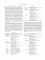
20 19
15
0
57 DR6iUPDATE
[31:0] Updated DR6
59
60
61
62
63
[31:0]
[31:0]
[31:0]
[31:0]
[31:0]
0
1
2
3
linear
linear
linear
linear
TCODE # TCODE Type
TDATA
0000
Missed Trace
0001
Conditional Branch
Contains Branch Sequence
0010
Branch Target
Contains Branch Target Address
0011
Previous Segment
Contains Previous Segment Base
Base
Address and Attributes
0100
0101
Current Segment Base Contains Current Segment Base
Address and Attributes
Interrupt
Contains Vector Number of Excep
0110
Trace Synchronization Contains Address of Most Recently
0111
Multiple Trace
1000
Trace Stop
35
Not Valid
tion or Interrupt
40
Executed Instruction
Contains 2nd or 3rd Record of Entry
With Multiple Records
Contains Instruction Address Where
Trace Capture Was Stopped
1001
1010
User Trace
Performance Pro?le
Contains User Speci?ed Trace Data
Contains Performance Pro?ling Data
45
50
The trace cache 200 is of limited storage capacity; thus a
certain amount of “compression” in captured trace data is
desirable. In capturing trace data, the folloWing discussion
assumes that an image of the program being traced is
available to the host system H. If an address can be obtained
55
from a program image (Object Module), then it is not
provided in the trace data. Preferably, only instructions
Which disrupt the instruction How are reported; and further,
only those Where the target address is in some Way data
dependent. For example, such “disrupting” events include
call instructions or unconditional branch instructions in
Which the target address is provided from a data register or
other memory location such as a stack.
address
address
address
address
As indicated in the preceding table, other desired trace
information includes: the target address of a trap or interrupt
handler; the target address of a return instruction; a condi
tional branch instruction having a target address Which is
data register dependent (otherWise, all that is needed is a
65
shoWn in Table 8 is not considered critical to the invention
In one contemplated embodiment of the invention, the
embedded processor device 102 reports eleven different
TABLE 9
30
60
The ordering or the presence of any particular command
|
trace codes as set forth in table 9:
Words
CR2
breakpoint
breakpoint
breakpoint
breakpoint
V may also be included. The TCODE ?eld is a code that
identi?es the type of data in the TDATA ?eld. The TDATA
?eld contains softWare trace information used for debug
purposes.
IV [TCODE (Trace Code)|TDATA (Trace Data)
12 DR6
13 DR7
CR2
DRO
DR1
DR2
DR3
When the parallel port is enabled and must be used for access
While the processor is executing instructions.
1-bit trace indicating if the branch Was taken or not); and,
most frequently, addresses from procedure returns. Other
information, such as task identi?ers and trace capture stop/
US 6,314,530 B1
17
18
start information, can also be placed in the trace cache 200.
The precise contents and nature of the trace records are not
considered critical to the invention.
FIG. 6A illustrates an exemplary format for reporting
conditional branch events. In the disclosed embodiment of
the invention, the outcome of up to 15 branch events can be
interrupted by generating a trace synchroniZation (TCODE=
0110) entry immediately prior to the interrupt entry, as Well
as the previous segment base address (TCODE=0011). The
trace synchroniZation entry contains the address of the last
instruction retired before the interrupt handler commences.
FIG. 6E illustrates a trace entry used to report a change in
segment parameters. When processing a trace stream in
accordance With the invention, trace address values are
grouped into a single trace entry. The 16-bit TDATA ?eld (or
“BFIELD”) contains 1-bit branch outcome trace entries, and
is labeled as a TCODE=0001 entry. The TDATA ?eld is
initially cleared except for the left most bit, Which is set to
10
1. As each neW conditional branch is encountered, a neW one
one branch every six instructions, the disclosed trace cache
200 therefore provides an effective trace record of 1,536
instructions. This estimate does not take into account the
occurrence of call, jump and return instructions.
In the disclosed embodiment of the invention, the trace
15
TCODE=0111 entry contains the loW 15 or 4 bits (depending
20
sor interface logic 202. When a branch target address must
be reported, information contained Within a current condi
tional branch TDATA ?eld is marked as complete by the
trace control logic 218, even if 15 entries have not accumu
There are circumstance When an application program or
operating system may Wish to add additional information
lated. As shoWn in FIG. 6B, the target address (in a
into a trace stream. For this to occur, an x86 instruction is
preferably provided Which enables a 16-bit data value to be
placed in the trace stream at a desired execution position.
recorded in a trace entry pair, With the ?rst entry (TCODE=
30
When the processor core 104 executes this instruction, the
for a conditional jump instruction, no 1-bit branch outcome
user speci?ed trace entry is captured by the trace control
logic 218 and placed in the trace cache 200. As shoWn in
trace entry appears for the reported branch.
35
When a task sWitch occurs in a multi-tasking operating
system.
40
disabling trace capture. For example, an x86 command can
be provided, or an existing x86 command can be utiliZed to
toggle a bit in an I/O port location. Alternatively, on-chip
breakpoint control registers (not shoWn) can be con?gured
45
to indicate the addresses Where trace capture should start/
stop. When tracing is halted, a trace entry (TCODE=1000,
TCODE=0111) recording the last trace address is placed in
the trace stream. When tracing is resumed, a trace synchro
niZation entry (TCODE=0110, TCODE=0111) containing
50
the address of the currently executing instruction is gener
ated.
It may be important to account for segment changes that
occur While tracing is stopped. This situation can be partially
resolved by selecting an option to immediately folloW a
TCODE=1000 entry With a current segment base address
55
entry (TCODE=0100, TCODE=0111), as shoWn in FIG. 6C.
A con?guration option is also desirable to enable a current
segment base address entry at the end of a trace prior to
entering Debug mode. By contrast, it may not be desirable
indicates the result of a conditional operation. When exam
ining a trace stream, hoWever, data can only be studied in
relation to a knoWn program address. For example, starting
With the oldest entry in the trace cache 200, all entries until
an address entry are of little use. Algorithm synchronization
typically begins from a trace entry providing a target
address.
The processor can provide trace synchroniZation infor
mation to ensure that address information for reconstructing
instruction execution How is provided in trace records With
suf?cient frequency. If the trace cache 200 contains no
entries providing an address, then trace analysis cannot
occur. This situation is rare, but possible. A trace record (or
an indication in a trace record), is provided for instructions
that change the program How such as conditional branches.
tion is not provided in the trace record for instructions such
as conditional branches Where the branch target address can
be determined according to Whether the branch Was taken or
not taken. In such cases, the trace record provides only an
indication of Whether the branch Was taken. Target or other
asynchronous or synchronous event such as an interrupt or
desirable to record the address of the instruction Which Was
When executing typical softWare on a processor-based
device 102 according to the disclosed embodiment of the
invention, feW trace entries contain address values. Most
entries are of the TCODE=0001 format, in Which a single bit
HoWever, as previously discussed, target address informa
60
to provide segment base information When the base has not
changed, such as When an interrupt has occurred.
Referring to FIG. 6D, folloWing the occurrence of an
trap, a TCODE=0101 trace entry is generated to provide the
address of the target interrupt handler. HoWever, it is also
FIG. 6F, a TCODE=1001 entry is used for this purpose in the
disclosed embodiment of the invention. This entry might
provide, for example, a previous or current task identi?er
execution; for example, When a task context sWitch occurs.
When trace capture is stopped, no trace entries are entered
into the trace cache 200, nor do any appear on the bond-out
pins of trace port 214.
Different methods are contemplated for enabling and
The instruction can be implemented as a move to I/O space,
With the operand being provided by memory or a register.
the target address. When a branch target address is provided
Referring noW to FIG. 6C, it may be desirable to start and
mode). The TCODE=0111 entry also preferably includes
bits indicating the current segment siZe (32-bit or 16-bit), the
operating mode (real or protected), and a bit indicating
Whether paging is being utiliZed. Segment information gen
erally relates to the previous segment, not a current (target)
segment. Current segment information is obtained by stop
ping and examining the state of the processor core 104.
processor-based device 102 using 32-bit addressing) is then
stop trace gathering during certain sections of program
of the previous segment base address, While the associated
on Whether the instruction is executed in real or protected
control logic 218 monitors instruction execution via proces
0010) providing the high 16-bits of the target address and the
second entry (TCODE=0111) providing the loW 16-bits of
default data operand siZe (32 or 16-bit mode), are subject to
change. As a result, the TCODE=0011 and 0111 entries are
con?gured to provide the information necessary to accu
rately reconstruct instruction ?oW. The TDATA ?eld corre
sponding to a TCODE=0011 entry contains the high 16-bits
bit entry is added on the left and any other entries are shifted
to the right by one bit.
Using a 128 entry trace cache 200 alloWs 320 bytes of
information to be stored. Assuming a branch frequency of
combined With a segment base address to determine an
instruction’s linear address. The base address, as Well as the
65
address information is provided, hoWever, for those instruc
tions in Which the target address is in some Way data
dependent and for other TCODES shoWn in Table 9.
US 6,314,530 B1
19
20
The processor determines Whether each trace record
applications. Exemplary operating systems include
includes target address information. Each trace entry having
Microsoft’s WindoWs CE (see BYTE, August 1997, pages
103—107); WindRiver’s VxWorks; RISC OS Which operates
target address information causes a counter to be loaded to
a predetermined value Which alloWs the counter to count the
on Acorn RISC machine (ARM) based computers such as
desired maximum number of trace records generated before
current program address information is provided. Thus,
the ARM610, ARM700, ARM7500 and StrongARM micro
processors (see BYTE, December 1996, pp 49—50); an
object oriented multi-threaded real time operating systemOS
depending on if the counter is con?gured as an up counter
or doWn counter, the counter is either loaded With Zero or the
maximum count, respectively. The counter counts each trace
record produced Which does not include target address
information. When the count of such trace records reaches
called EPOC32 available from Psion SoftWare PLC (see
10
the predetermined number; trace logic provides the current
program address as a trace entry, thereby providing the trace
synchroniZation information.
For this reason, a synchroniZation register TSYNC is
15
provided to alloW injection of synchroniZing address infor
BYTE October 1997, pp. 45—46).
In a multi-tasking operating system, the kernel typically
provides basic services such as memory allocation, interrupt
handling functions, allocating system resources, controls
launching of various executable threads. An exemplary
operating system is shoWn in block diagram form in FIG. 7,
Which is a WindoWs CE-like operating system. Operating
systems for real time systems are typically highly modular
to alloW minimum con?gurations to be achieved for embed
mation. In the disclosed embodiment, TSYNC contains 7
bits. If the synchroniZation register TSYNC is set to Zero,
then trace synchroniZation entries are not generated.
ded systems.
The various parts of the operating system include device
drivers 703, communications services 705, graphics support
6
O
707 and additional components. The kernel 701 provides the
TSYNC (Trace Synchronization)
basic services previously described and in one embodiment
FIG. 6G depicts an exemplary trace synchroniZation
record. The ?rst entry, With a TCODE=6, provides the most
25
is a multi-threaded, and supports preemptive multi-tasking.
For example, the kernel Will respond to an interrupt by
launching the appropriate interrupt handler or thread.
Abstraction layer 709 provides an interface betWeen a
particular OEM’s hardWare and the kernel. The abstraction
signi?cant 16 bits of the extended instruction pointer (EIP)
for the current instruction logical address. The next entry,
layer may also provide poWer management features and
TCODE=7, provides the least signi?cant 16 bits.
interrupt services. Because it is advantageous for an oper
ating system to be able to run on a variety of microprocessor
platforms, the hardWare abstraction level alloWs the operat
Trace entry information can also be expanded to include
data relating to code coverage or execution performance.
This information is useful, for example, for code testing and
performance tuning. Even Without these enhancements, it is
ing system to exploit the particular implementation for
desirable to enable the processor core 104 to access the trace
platforms. One such implementation is described herein.
cache 200. In the case of a microcontroller device, this
access to a trace cache that may evolve on different hardWare
35
feature can be accomplished by mapping the trace cache 200
Within a portion of I/O or memory space. A more general
approach involves including an instruction Which supports
moving trace cache 200 data into system memory.
Device drivers 703 are built-in device support for input/
output such as keyboards and other devices. Object stores
713 provide such storage as ?le systems, registry and
database support. Communications 705 can provide LAN
connectivity, TCP/IP, PPP and other communications sup
port. The remote AOIs provide desktop devices utiliZing
OPERATING SYSTEM AND DEBUGGER
INTEGRATION
desktop operating systems such as WindoWs to access
WindoWs CE devices. The shells 717 provides shells (e.g.
It is advantageous to integrate debug support into the
operating system (OS). Speci?cally, the operating system
45
similar components and can readily be adapted to incorpo
rate the support for debug hooks described herein.
In addition to the kernel, other application task(s) 711 run
on the system. Getting systems running that include a
according to the present invention exploits the hardWare
and/or microcoded support for debug and particularly for
accessing trace memory 200. The debug support may go in
the kernel of the OS, may exist as a separate task in the OS
or may be a combination of both. The debug support in the
multi-tasking operating system involves debugging in steps.
OS provides such capabilities typically associated With
debug mode operations such as accessing registers and
memory locations. The operating system also provides
access to the trace memory 200 Which provides substantial
advantages as discussed further herein. For example, With
WindoWs) if needed for the particular application.
Many other operating systems mentioned earlier have
55
First the kernel is debugged. Once the kernel is debugged
and the debug softWare provided With the OS can be
successfully utiliZed, one can begin application mode
debugging. Often there are difficult tool transitions required
as debugging proceeds from kernel-mode to application
access to trace information, the operating system can even
mode.
analyZe trace records provided in trace memory 200. If an
operating system can control the on-chip trace memory 200
Which records program execution, the integration of an
ICE-like trace capability With operating system behavior can
Incorporating debug support directly into the OS to
exploit on-chip debug logic enables an operating system to
be free from the typical restrictions imposed by ROM
be successfully achieved. Thus, superior debug capability
install a monitor in a reserved memory region before com
monitors. Such an operating system avoids the need to ?rst
can be provided With substantial savings in costs because no
mencing kernel and driver con?guration for the system
external expensive ICE like support hardWare is necessary.
As discussed previously, the number of embedded sys
tems making use of multi-tasking operating systems is
being debugged. Thus embedded tool users Will be attracted
groWing. Anumber of multi-tasking operating systems (OS)
are knoWn Which are suitable for embedded and other
to such an operating system. Debugging can start immedi
65
ately With a system running from RAM With nothing pre
insalled in the target memory system. The debug port taught
in the present invention is usable at all Stages of debug,