1
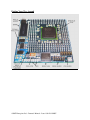
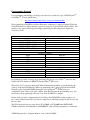
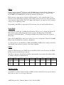
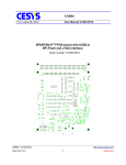
Darnaw1 User Manual
Issue – 1.00
©2007 Enterpoint Ltd. – Darnaw1 Manual – Issue 1.00 12/12/2007
Kit Contents
You should receive the following items with you Darnaw1 development kit:
1 - Darnaw1 Board.
©2007 Enterpoint Ltd. – Darnaw1 Manual – Issue 1.00 12/12/2007
Foreword
PLEASE READ THIS ENTIRE MANUAL BEFORE PLUGGING IN
OR POWERING UP YOUR DARNAW1 BOARD.
PLEASE TAKE SPECIAL NOTE OF THE WARNINGS WITHIN
THIS MANUAL.
Trademarks
Coolrunner-II, Spartan, ISE, EDK, Webpack, Xilinx are the registered trademarks of Xilinx Inc,
San Jose, California, US.
Darnaw1 is a trademark of Enterpoint Ltd.
©2007 Enterpoint Ltd. – Darnaw1 Manual – Issue 1.00 12/12/2007
Introduction
Welcome to your Darnaw1 board. Darnaw1 is a highly featured SpartanTM-3 FPGA
module, in Pin Grid array (PGA) format, supporting a large number of unallocated
I/O for user use.
The aim of this manual is to assist in using the main features of Darnaw1. Should this
manual fail to explain a feature sufficiently then our support team can be reached by
email on [email protected].
©2007 Enterpoint Ltd. – Darnaw1 Manual – Issue 1.00 12/12/2007
Finding Your Way Around
©2007 Enterpoint Ltd. – Darnaw1 Manual – Issue 1.00 12/12/2007
Getting Started
(1) Ensure that any vital data, contained within your host system, is backed up before attempting to
use your Darnaw1 in the system.
(2) Ensure that your host board for the Darnaw1 supplies bank voltages and main 3.3V power input
to the Darnaw1.
(3) Ensure that any signals that you are going input to Darnaw1 (a) do not exceed 3.5V (b) do not
exceed 3.3V I/P power voltage + 0.5V.
(4) Carefully plug, or solder, your Darnaw1 into the host board taking care not to bend pins of the
Darnaw1. Sockets, including ZIF type, can be bought if you do not want to solder the module
directly. Ensure the polarity of the Darnaw1 is correct when plugging in or soldering.
©2007 Enterpoint Ltd. – Darnaw1 Manual – Issue 1.00 12/12/2007
Darnaw1 Features
Power Inputs and Power Supplies
Darnaw1 uses a single 3.3V supply as power source and this is feed into the module on PGA pins
A11-14 and B11-14. The associate DGND/0V is connected on PGA pins C11-14 and D11-14.
The on-board TPS70402 twin regulator chip derives from the input supply 1.22V and 2.5V which
are used on the module for The SpartanTM-3E as core voltage and Vccaux supplies respectively.
The 1.22V supply is available for external use, monitoring, or for Bank Voltage use via PGA pins
C1, B2 and A3. The total current capability (including internal use) of this power rail is 2 amps
subject to thermal limitation.
The 2.5V supply is available for external use, monitoring, or for Bank Voltage use via PGA pins
A1, A2 and B1. The total current capability (including internal use) of this power rail is 1 amp
subject to thermal limitation.
Bank0 requires an input voltage to be fed in on PGA pins L18 and M18. You may use the main
3.3V as input or wire on your hosting board the 2.5V/1.22V output of the Darnaw1 to these pins.
You can also wire any other voltage within normal operating range of the SpartanTM-3E.
Bank1 requires an input voltage to be fed in on PGA pins V10 and V11. You may use the main
3.3V as input or wire on your hosting board the 2.5V/1.22V output of the Darnaw1 to these pins.
You can also wire any other voltage within normal operating range of the SpartanTM-3E.
Bank2 requires an input voltage to be fed in on PGA pins L4, M4 and N4. If you are using the
Serial Flash on board it is recommended that 3.3V is input to this bank. The Serial Flash normally
requires 2.7V (specification) or greater to operate but it may be possible to in practise to operate this
bank at 2.5V if necessary. Operation of the Serial Flash at 2.5V is not guaranteed.
WARNING – THE REGULATORS CAN GET VERY HOT IN
NORMAL OPERATION ALONG WITH THE BOARDS THERMAL
RELIEF. PLEASE DO NOT TOUCH OR PLACE HIGHLY
FLAMABLE MATERIALS NEAR THESE DEVICES WHILST THE
DARNAW1 MODULE IS IN OPERATION.
©2007 Enterpoint Ltd. – Darnaw1 Manual – Issue 1.00 12/12/2007
Selecting the FPGA Bank (VCCIOX) voltages.
Darnaw1 fixes the I/O voltage of FPGA bank 3 to 3.3V.
FPGA banks 0, 1 and 2 are supplied by the hosting board and can be anywhere in the normal
SpartanTM-3E operating range.
Please note the limitations of the Serial Flash (ST Microelectronics M25P16) is a minimum of 2.8V
and it is on the Bank2 power supply. Failure to meet this may mean that the Darnaw1 FPGA does
not configure.
©2007 Enterpoint Ltd. – Darnaw1 Manual – Issue 1.00 12/12/2007
Programming Darnaw1
For programming and building your design you will need to download a copy of ISE WebpackTM
form XilinxTM. You can obtain it here:
http://www.xilinx.com/ise/logic_design_prod/webpack.htm
The programming of the FPGA and Serial Flash parts on Darnaw1 is achieved separate JTAG and
Serial Flash interfaces. These interfaces appear on connectors J3 (Serial Flash) and J2 (JTAG). The
interfaces also appear on PGA pins allowing programming via the hosting board. Signals are
located as follows:
Serial Flash Programming
Signal
PROG_B
SPI_SD_IN(FPGA-MOSI)
SP_SD_OUT(FPGA-DIN)
SPI_SCLK(FPGA-CCLK)
SPI_CS_N(FPGA-CS0_B)
PGA Pin
A9
B4
B3
B6
A5
JTAG Programming
Signal
TDI
TMS
TCK
TDO
PGA Pin
Y21
Y20
AA20
AA21
Other Useful Signals
Signal
INIT_B
DONE
PGA Pin
A4
N/A
Programming is carried out using our programming cable Prog2 or any XilinxTM cable later than
Parallel Cable IV and the tool IMPACT from the XilinxTM ISE toolset.
The headers J2, J3 conform to the normal Xilinx standard pinout with the exception that Prog_B
signal is on the Serial Flash header. When a programming cable is plugged into the Serial Flash
header Prog_B is held at 0V/DGND placing the on-board SpartanTM-3E FPGA into preconfiguration mode. This avoids drive conflicts of the FPGA against the programming cable. You
must remove the programming cable from J3 to allow the FPGA to configure.
Header J4 also provides a manual method to hold Prog_B at 0V/DGND by fitting a jumper over
pins 1 and 2 of this header. Pin3 is provided as jumper store and fitting a jumper in pins 2 and 3 will
have no effect.
The JTAG chain will report a single device XC3S1200E or XC3S1600E when INITIALISE
CHAIN command is used within the tool ISE IMPACT. Direct JTAG programming is volatile and
©2007 Enterpoint Ltd. – Darnaw1 Manual – Issue 1.00 12/12/2007
the FPGA will lose its configuration every time the board power is cycled. From sustained use of
FPGA design programming the design into the Serial Flash memory is recommended. Generation
of suitable Serial Flash content files and control of the JTAG chain can be achieved using the
XILINX ISE tool IMPACT.
The standard device in the Serial Flash position is the ST Microelectronics M25P16.
©2007 Enterpoint Ltd. – Darnaw1 Manual – Issue 1.00 12/12/2007
FPGA
Darnaw1 supports SpartanTM-3E devices in the FGG400 package. Standard builds of Darnaw1 use
commercial grade devices but industrial grade parts can be fitted at extra cost. Currently either
XC3S1200E or XC3S1600E devices are fitted as standard to the Darnaw1.
FPGA reference voltage pins are available for FPGA banks 0, 1, and 2 on the PGA pins. To use
reference voltages the hosting board must connect all I/Os, that are used as Vref, in any given bank
to the reference voltage required. The 1.22V output of the Darnaw1 can often be used as a reference
voltage for 2.5V signalling systems.
Programming of the FPGA is supported by JTAG and from serial on-board Serial Flash devices.
Serial Flash
Your Darnaw1 normally has a 16 MBit Serial Flash fitted. This is used to configure the Spartan-3E
FPGA but the portion of this device unused can be used as code/data storage for embedded
microprocessors like MicroBlazeTM. Normally the M25P16 from ST Microelectronics is fitted in
this position.
When a XC3S1200E FPGA is fitted 3,841,184 bits are used for configuration. When a XC3S1600E
FPGA is fitted 5,969,696 bits are used for configuration.
As a build option we can fit M25P32 (32 MBit) and M25P64 (64 MBit) devices in this position and
other suitable vendor devices to increase code storage capability.
LEDS
Supplied on Darnaw1 there are 8 LEDS driven by the FPGA. LED1 cannot be driven by the FPGA
but may be driven by the PGA pin on the net.
The LED1 is adjacent to Serial Flash and LEDs count in number away from the Serial Flash. LEDs
are situated on IO pins as indicated below.
LED
PGA
PIN
FPGA
PIN
LED1
G1
LED2
G2
LED3
G3
LED4
G4
LED5
F1
LED6
F2
LED7
F3
LED8
F4
T10
Y9
W9
V9
Y8
W8
V2
Y7
OSCILLATOR
A standard 7x5 oscillator is fitted. Usually a 32 MHz oscillator is fitted. We can do special values in
this position at extra cost or for large volume runs.
©2007 Enterpoint Ltd. – Darnaw1 Manual – Issue 1.00 12/12/2007
SDRAM MEMORY
Normally a 128 MBit SDRAM from Micron Technology or ISSI is fitted. This device is X32
organisation and operates from the 3.3V input supply.
The device is connected to Bank3 of the FPGA. The pin connections can be found in the Darnaw1
schematics linked off the Darnaw1 product page:
http://www.enterpoint.co.uk/moelbryn/darnaw1.html
©2007 Enterpoint Ltd. – Darnaw1 Manual – Issue 1.00 12/12/2007
Medical and Safety Critical Use
Darnaw1 boards are not authorised for the use in, or use in the design of, medical or other safety
critical systems without the express written person of the Board of Enterpoint. If such use is
allowed the said use will be entirely the responsibility of the user. Enterpoint Ltd will accept no
liability for any failure or defect of the Darnaw1 board, or its design, when it is used in any medical
or safety critical application.
Warranty
Darnaw1 comes with a 90 return to base warranty.
Other specialised warranty programs can be offered to users of multiple Enterpoint products. Please
contact sales on [email protected] if you are interested in these types of warranty,
Support
Enterpoint offers support during normal United Kingdom working hours 9.00am to 5.00pm. Please
examine our Darnaw1 FAQ web page and the contents of this manual before raising a support
query. We can be contacted as follows:
Telephone
Email
- +44 (0) 1684 585262
- [email protected]
©2007 Enterpoint Ltd. – Darnaw1 Manual – Issue 1.00 12/12/2007