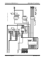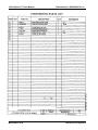
1
RACAL INSTRUMENTS™ 1260A OPT 01T Publication No. 980806-999 Rev. A Astronics Test Systems Inc. 4 Goodyear, Irvine, CA 92618 Tel: (800) 722-2528, (949) 859-8999; Fax: (949) 859-7139 [email protected] [email protected] [email protected] http://www.astronicstestsystems.com Copyright 1996 by Astronics Test Systems Inc. Printed in the United States of America. All rights reserved. This book or parts thereof may not be reproduced in any form without written permission of the publisher. THANK YOU FOR PURCHASING THIS ASTRONICS TEST SYSTEMS PRODUCT For this product, or any other Astronics Test Systems product that incorporates software drivers, you may access our web site to verify and/or download the latest driver versions. The web address for driver downloads is: http://www.astronicstestsystems.com/support/downloads If you have any questions about software driver downloads or our privacy policy, please contact us at: [email protected] WARRANTY STATEMENT All Astronics Test Systems products are designed to exacting standards and manufactured in full compliance to our AS9100 Quality Management System processes. This warranty does not apply to defects resulting from any modification(s) of any product or part without Astronics Test Systems express written consent, or misuse of any product or part. The warranty also does not apply to fuses, software, non-rechargeable batteries, damage from battery leakage, or problems arising from normal wear, such as mechanical relay life, or failure to follow instructions. This warranty is in lieu of all other warranties, expressed or implied, including any implied warranty of merchantability or fitness for a particular use. The remedies provided herein are buyer’s sole and exclusive remedies. For the specific terms of your standard warranty, contact Customer Support. Please have the following information available to facilitate service. 1. Product serial number 2. Product model number 3. Your company and contact information You may contact Customer Support by: E-Mail: [email protected] Telephone: +1 800 722 3262 (USA) Fax: +1 949 859 7139 (USA) RETURN OF PRODUCT Authorization is required from Astronics Test Systems before you send us your product or sub-assembly for service or calibration. Call or contact Customer Support at 1-800-722-3262 or 1-949-859-8999 or via fax at 1-949859-7139. We can also be reached at: [email protected]. If the original packing material is unavailable, ship the product or sub-assembly in an ESD shielding bag and use appropriate packing materials to surround and protect the product. PROPRIETARY NOTICE This document and the technical data herein disclosed, are proprietary to Astronics Test Systems, and shall not, without express written permission of Astronics Test Systems, be used in whole or in part to solicit quotations from a competitive source or used for manufacture by anyone other than Astronics Test Systems. The information herein has been developed at private expense, and may only be used for operation and maintenance reference purposes or for purposes of engineering evaluation and incorporation into technical specifications and other documents which specify procurement of products from Astronics Test Systems. TRADEMARKS AND SERVICE MARKS All trademarks and service marks used in this document are the property of their respective owners. • Racal Instruments, Talon Instruments, Trig-Tek, ActivATE, Adapt-A-Switch, N-GEN, and PAWS are trademarks of Astronics Test Systems in the United States. DISCLAIMER Buyer acknowledges and agrees that it is responsible for the operation of the goods purchased and should ensure that they are used properly and in accordance with this document and any other instructions provided by Seller. Astronics Test Systems products are not specifically designed, manufactured or intended to be used as parts, assemblies or components in planning, construction, maintenance or operation of a nuclear facility, or in life support or safety critical applications in which the failure of the Astronics Test Systems product could create a situation where personal injury or death could occur. Should Buyer purchase Astronics Test Systems product for such unintended application, Buyer shall indemnify and hold Astronics Test Systems, its officers, employees, subsidiaries, affiliates and distributors harmless against all claims arising out of a claim for personal injury or death associated with such unintended use. FOR YOUR SAFETY Before undertaking any troubleshooting, maintenance or exploratory procedure, read carefully the WARNINGS and CAUTION notices. This equipment contains voltage hazardous to human life and safety, and is capable of inflicting personal injury. If this instrument is to be powered from the AC line (mains) through an autotransformer, ensure the common connector is connected to the neutral (earth pole) of the power supply. Before operating the unit, ensure the conductor (green wire) is connected to the ground (earth) conductor of the power outlet. Do not use a two-conductor extension cord or a three-prong/two-prong adapter. This will defeat the protective feature of the third conductor in the power cord. Maintenance and calibration procedures sometimes call for operation of the unit with power applied and protective covers removed. Read the procedures and heed warnings to avoid “live” circuit points. Before operating this instrument: 1. Ensure the proper fuse is in place for the power source to operate. 2. Ensure all other devices connected to or in proximity to this instrument are properly grounded or connected to the protective third-wire earth ground. If the instrument: - fails to operate satisfactorily shows visible damage has been stored under unfavorable conditions has sustained stress Do not operate until performance is checked by qualified personnel. Publication No. 980806-999 Rev. A 1260A Option 01T User Manual Table of Contents Chapter 1 ................................................................................................................................. 1-1 GETTING STARTED ......................................................................................................................... 1-1 Overview ......................................................................................................................................... 1-1 Items Shipped with the 1260A Option-01T ................................................................................ 1-1 Installation and Setup ................................................................................................................. 1-1 Installing the Option-01T into a Switch Module ...................................................................... 1-1 Logical Address Switches ....................................................................................................... 1-3 Interrupt Level ......................................................................................................................... 1-4 Module Address Switches....................................................................................................... 1-5 VXI Local Bus Connections .................................................................................................... 1-6 Bus Grant Connections ........................................................................................................... 1-8 Local Bus Lockout Keys.......................................................................................................... 1-9 Installing the Switch Modules................................................................................................ 1-11 Switch Module Connections ................................................................................................. 1-11 Communicating with the Switch Modules ................................................................................. 1-13 Activating VXI Chassis Power............................................................................................... 1-13 Communicating via the VXIbus ............................................................................................. 1-13 Switch Controller Self-Test ................................................................................................... 1-17 Resetting the Switch Modules ........................................................................................... 1-17 Selecting Relays to Operate ............................................................................................. 1-18 Module Addresses............................................................................................................. 1-18 Channels ........................................................................................................................... 1-19 Channel Designators ......................................................................................................... 1-19 Closing a Relay ................................................................................................................. 1-20 Opening a Relay ................................................................................................................ 1-20 Astronics Test Systems i 1260A Option 01T User Manual Publication No. 980806-999 Rev. A Chapter 2 ................................................................................................................................. 2-1 USING THE OPTION-01T ................................................................................................................. 2-1 Register-Based Operation and Message-Based Operation .......................................................... 2-1 Message-Based Operation ............................................................................................................ 2-2 SCPI Command Overview .......................................................................................................... 2-2 Command Keyword Long Form and Short Form ....................................................................... 2-3 Case Sensitivity....................................................................................................................... 2-4 Optional Keywords .................................................................................................................. 2-4 Querying Parameter Setting ................................................................................................... 2-4 SCPI Command Terminator ................................................................................................... 2-5 IEEE-STD-488.2 Common Commands .................................................................................. 2-5 SCPI Parameter Type ............................................................................................................. 2-5 Numeric Parameters ........................................................................................................... 2-5 Discrete Parameters............................................................................................................ 2-6 Boolean Parameters............................................................................................................ 2-7 Command Input Buffer ............................................................................................................ 2-7 Reply Output Buffer................................................................................................................. 2-8 Reading Error Messages ............................................................................................................ 2-9 Specifying Channels in Commands ......................................................................................... 2-10 Naming Relay Cards ................................................................................................................. 2-12 Defining Module Names........................................................................................................ 2-12 Removing Module Names..................................................................................................... 2-13 Reading the Presently Defined Module Names ................................................................... 2-13 Reading the Module Address for a Module Name ............................................................... 2-14 Storing the Module Names in Nonvolatile Memory .............................................................. 2-14 Naming a Path ...................................................................................................................... 2-15 Defining Path Names ........................................................................................................ 2-15 Removing Path Names ..................................................................................................... 2-16 ii Astronics Test Systems Publication No. 980806-999 Rev. A 1260A Option 01T User Manual Reading the Presently Defined Path Names .................................................................... 2-16 Reading the Channel List for a Path Name ...................................................................... 2-17 Storing the Path Names in Nonvolatile Memory ............................................................... 2-17 Closing Relays ...................................................................................................................... 2-17 Opening Relays ..................................................................................................................... 2-18 Include Lists .............................................................................................................................. 2-19 Exclude Lists ............................................................................................................................. 2-22 Scan Lists ................................................................................................................................. 2-24 Defining a Scan List .............................................................................................................. 2-26 Selecting the Trigger Source ................................................................................................ 2-28 Selecting the Trigger Count .................................................................................................. 2-29 Selecting a Trigger Delay...................................................................................................... 2-30 Arming and Disarming the Option-01T ................................................................................. 2-30 Generating a Single Trigger .............................................................................................. 2-32 Output Trigger Signals from the Option-01T..................................................................... 2-33 Selecting an Output Trigger Destination ........................................................................... 2-33 Selecting the Order of Relay Operations .............................................................................. 2-34 Relay Readback and Monitoring ........................................................................................... 2-35 Digital Module Operation .......................................................................................................... 2-36 Digital Module Ports .............................................................................................................. 2-37 Asynchronous Digital Operation ........................................................................................... 2-37 Synchronous Digital Operation ............................................................................................. 2-37 Mixing Synchronous and Asynchronous Modes of Operation ............................................. 2-38 Specifying Ports on a Digital Module .................................................................................... 2-38 Selecting the Mode of Operation .......................................................................................... 2-39 Enabling and Disabling the Ports.......................................................................................... 2-40 Using the Asynchronous Mode of Operation ........................................................................ 2-41 Using the Synchronous Mode of Operation.......................................................................... 2-42 Setting Up the Synchronous Test ......................................................................................... 2-44 Astronics Test Systems iii 1260A Option 01T User Manual Publication No. 980806-999 Rev. A Arming the Digital Modules ................................................................................................... 2-48 Checking for Data Transfer Completion ............................................................................... 2-49 Reading Data from a Synchronous Input Port ...................................................................... 2-49 Clearing Data from Synchronous Input and Output Ports .................................................... 2-50 Synchronous Control and Status Pins .................................................................................. 2-51 Synchronous and Asynchronous Example ........................................................................... 2-51 IEEE 488.2 Common Commands ........................................................................................ 2-53 IEEE-488.2 Status Description ............................................................................................. 2-54 *CLS Command ................................................................................................................ 2-60 *ESE Command ................................................................................................................ 2-61 *ESE? Query ..................................................................................................................... 2-62 *ESR? Query ..................................................................................................................... 2-62 *SRE Command ................................................................................................................ 2-62 *SRE? Query ..................................................................................................................... 2-62 *STB? Query ..................................................................................................................... 2-63 *OPC Command ................................................................................................................ 2-63 *OPC? Query..................................................................................................................... 2-63 *IDN? Query ...................................................................................................................... 2-64 *RST Command ................................................................................................................ 2-64 *TST? Query...................................................................................................................... 2-65 *RCL Command ................................................................................................................ 2-65 *SAV Command ................................................................................................................ 2-66 *TRG Command ................................................................................................................ 2-66 *WAI Command ................................................................................................................ 2-66 SCPI Status Registers .......................................................................................................... 2-67 SCPI and IEEE 488.2 Status Indicators............................................................................ 2-68 Register-Based Operation .................................................................................................... 2-69 Communicating via Register-Based Mode ....................................................................... 2-69 VISA and the VXIplug&play Software ................................................................................... 2-79 iv Astronics Test Systems Publication No. 980806-999 Rev. A 1260A Option 01T User Manual Working with Both Register-Based and Message-Based Modes ........................................ 2-82 Setting the Interrupt Level ................................................................................................. 2-83 Chapter 3 ................................................................................................................................. 3-1 COMMAND REFERENCE ................................................................................................................. 3-1 General ........................................................................................................................................... 3-1 Chapter 4 ................................................................................................................................. 4-1 FUNCTIONAL DESCRIPTION .......................................................................................................... 4-1 Introduction ..................................................................................................................................... 4-1 Features ...................................................................................................................................... 4-2 Theory of Operation ....................................................................................................................... 4-4 Functional Blocks........................................................................................................................ 4-4 Reset/Voltage Monitor ............................................................................................................ 4-4 VXI Application-Specific Integrated Circuit (VXI ASIC) .......................................................... 4-5 Clock Selection Logic.............................................................................................................. 4-5 Microprocessor........................................................................................................................ 4-6 Address Decoder .................................................................................................................... 4-7 Static RAM .............................................................................................................................. 4-8 PROM...................................................................................................................................... 4-8 Non-Volatile RAM.................................................................................................................... 4-8 Interval Timer .......................................................................................................................... 4-9 External Trigger Logic ............................................................................................................. 4-9 Discrete Input Register ......................................................................................................... 4-11 Discrete Output Register....................................................................................................... 4-11 Logical Address DIP Switches .............................................................................................. 4-11 Local Bus Controller/Interrupt Priority Encoder .................................................................... 4-12 Test Port ................................................................................................................................ 4-14 Astronics Test Systems v 1260A Option 01T User Manual Publication No. 980806-999 Rev. A Chapter 5 ................................................................................................................................. 5-1 MAINTENANCE ................................................................................................................................. 5-1 Introduction ..................................................................................................................................... 5-1 Indented Parts List ...................................................................................................................... 5-1 16MHz Option-01T .................................................................................................................. 5-1 Drawings ..................................................................................................................................... 5-2 Parts Lists ................................................................................................................................. 5-23 vi Astronics Test Systems Publication No. 980806-999 Rev. A 1260A Option 01T User Manual Appendix A..............................................................................................................................A-1 SPECIFICATIONS .............................................................................................................................A-1 General ...........................................................................................................................................A-1 Processor ....................................................................................................................................A-1 Mechanical ..................................................................................................................................A-1 Power and Cooling .....................................................................................................................A-2 Environment ................................................................................................................................A-2 EMC and Safety ..........................................................................................................................A-2 Reliability.....................................................................................................................................A-2 Appendix B..............................................................................................................................B-1 ERROR MESSAGES .........................................................................................................................B-1 General ...........................................................................................................................................B-1 Appendix C ............................................................................................................................ C-1 IN CASE OF TROUBLE.................................................................................................................... C-1 General .......................................................................................................................................... C-1 Appendix D ............................................................................................................................ D-1 MODULES ........................................................................................................................................ D-1 General .......................................................................................................................................... D-1 Astronics Test Systems vii 1260A Option 01T User Manual Publication No. 980806-999 Rev. A This page was left intentionally blank. viii Astronics Test Systems Publication No. 980806-999 Rev. A 1260A Option 01T User Manual Table of Figures Figure 1-1, Installing the Option–01T ................................................................................................ 1-3 Figure 1-2, Setting the Option-01T Logical Address ......................................................................... 1-4 Figure 1-3, Local Bus Jumper Switches and Module Address Switches .......................................... 1-6 Figure 1-4, Installing the Bus Grant and Local Bus Jumpers ............................................................ 1-8 Figure 1-5, Local Bus Daisy-Chaining ............................................................................................... 1-9 Figure 1-6, Local Bus Lockout Keys ................................................................................................ 1-10 Figure 1-7, Local bus Key Installation.............................................................................................. 1-10 Figure 1-8, Switch Module Installation ............................................................................................. 1-12 Figure 1-9, Sample Execution of the Resource Manager Program (Part 1) ................................... 1-15 Figure 2-1, State Transition Diagram For Arming and Triggering the Option-01T ......................... 2-32 Figure 2-2 (A), Port 4 Data After “DIG:SYNC:DATA (@7(4)),10,20,30,40" .......................... 2-45 Figure 2-2 (B), Port 4 Data After “DIG:SYNC:DATA (@7(4)),50,60,70,80,90" ................... 2-46 Figure 2-2 (C), Port 4 Data After “DIG:SYNC:INDEX (@7(4)),3" ............................................. 2-46 Figure 2-2 (D), Port 4 Data After “DIG:SYNC:DATA (@7(4)),77,78" ....................................... 2-47 Figure 2-3, IEEE-488.2 Status Reporting Model ............................................................................. 2-55 Figure 2-4, Sample Resource Manager Display.............................................................................. 2-70 Figure 4-1, 1260 Series Data Paths .................................................................................................. 4-2 Figure 4-2, Option-01T Features ....................................................................................................... 4-3 Astronics Test Systems ix 1260A Option 01T User Manual Publication No. 980806-999 Rev. A This page was left intentionally blank. x Astronics Test Systems Publication No. 980806-999 Rev. A 1260A Option 01T User Manual List of Tables Table 1-1, Attributes, Related Commands, and Reset State .......................................................... 1-18 Table 2-1, Power-On and Reset State ............................................................................................ 2-64 Table 2-2, Base Address for 1260 Series Modules ......................................................................... 2-71 Table 2-3, Control Register Offsets for Sample 1260 Series Module ............................................. 2-72 Table 2-4, Partial Data for the 1260-40A ......................................................................................... 2-74 Table 2-5, Control Data for Sample 1260 Module ........................................................................... 2-76 Table 2-6, Partial Data for the 1260-54 ........................................................................................... 2-77 Table 3-1, Commands Implemented by the Option-01T ................................................................... 3-3 Table 4-1, Changing the Clock Frequency ........................................................................................ 4-6 Table 4-2, Chip Select Signal Names ................................................................................................ 4-7 Table 4-3, Discrete Output Register Bits ......................................................................................... 4-10 Table 4-4, TTL Control ..................................................................................................................... 4-10 Table 4-5, Test Signals .................................................................................................................... 4-14 Table 4-6, Bit Patterns ..................................................................................................................... 4-16 Table B-1, Error Messages ................................................................................................................B-2 Table C-1, Trouble Shooting............................................................................................................. C-2 Astronics Test Systems xi 1260A Option 01T User Manual Publication No. 980806-999 Rev. A DOCUMENT CHANGE HISTORY Revision A xii Date Description of Change 04/28/09 Revised per EO 29692 Revised format to current standards. Company name revised throughout manual. Manual now revision letter controlled. Added Document Change History Page xi. Back of cover sheet. Revised Warranty Statement, Return of Product, Proprietary Notice and Disclaimer to current standards. Removed (Chap 6). Information. Now appears in first 2 pages behind cover page. Updated table of contents to reflect changes made. Added to footer company name… to lower corner opposite of Page no’s i thru xii. Astronics Test Systems Publication No. 980806-999 Rev. A 1260A Option 01T User Manual Chapter 1 GETTING STARTED Overview The 1260 Series consists of a variety of relay switching modules, the 1260-14 digital test module, and the Option-01T switch module controller. Up to twelve 1260-Series modules may be installed into a VXI chassis. A single 1260A Option-01T controls all 1260-Series modules in the VXI chassis. The Option-01T is installed only inside the module that occupies the left-most chassis slot in the group. When the slot 0 controller sends a command to the Option-01T, 25 the Option-01T responds by communicating with the appropriate switch modules to open or close relays, or to verify status of the relays. Items Shipped with the 1260A Option-01T The following items are shipped with the 1260A Option-01T: • 1260A Option-01T PCB Assembly: • with 16 MHZ CPU: P/N 405108-001 • Operating Manual: Publication number 980806-999 Installation and Setup Installing the Option01T into a Switch Module If you purchase your Option-01T and a 1260-Series module together, then the switch module is shipped with the Option-01T pre-installed. If this is the case, skip to the next subsection: Logical Address Switches. Otherwise, install the Option-01T into the 1260-Series module as follows. First, if you are using more than one 1260-Series switch module, decide how you will arrange the modules in the VXI chassis. Keep in mind that a single Option-01T can control up to twelve 1260-Series switch modules. This requires that all 1260-Series modules be placed in a contiguous group, i.e., with no other modules or empty slots Astronics Test Systems Getting Started 1-1 1260A Option 01T User Manual Publication No. 980806-999 Rev. A between them. Also, the switch module containing the Option-01T must be the left-most module of the group. CAUTION: ALWAYS PERFORM DISASSEMBLY, REPAIR AND CLEANING AT A STATIC SAFE WORKSTATION. Once you have decided which switch module will contain the Option01T, refer to Figure 1-1 for installation: Getting Started 1-2 (1) Remove the top and bottom covers of the switch module. (2) Remove the jumper board (P/N 401951) fitted to connector J4 on the switch module. For the 1260-40, remove the jumpers that are installed in connector J4. (3) Remove the jumper board (P/N 401951-003) fitted to connector J3 on the switch module. (4) Align the Option-01T connectors with those on the switch module: P3 to J3, and P4 to J4. Press the Option-01T firmly onto the switch module, taking care not to bend or damage any pins on the connectors. (5) Secure the Option-01T to the switch module using the three screws provided (See Figure 1-1). (6) Install the SYSFAIL indicator cable supplied with the Option-01T (See Figure 1-1). Connect the three-pin connector to the threepin plug on the Option-01T (the cable is wired so that the indicator will work properly regardless of which way the three-pin connector is plugged in). Locate the hole marked FAIL at the top of the switch module front panel. Insert the LED into the hole from the front of the panel, so that the pins point into the module. Press gently on the front of the LED until it snaps in place. Then plug the two-pin connector of the SYSFAIL cable into the LED. The long lead of the LED connects to the Black wire lead of the Connector. (7) Reinstall the top and bottom covers of the switch module. Astronics Test Systems Publication No. 980806-999 Rev. A 1260A Option 01T User Manual Figure 1-1, Installing the Option-01T Logical Address Switches A logical address is a number from 1 to 254, inclusive, assigned to a VXI module. Generally, each VXI module must have unique logical address assigned to it. The slot 0 controller uses logical addresses to distinguish one module from other modules in the same VXI chassis. Since the Option-01T communicates directly with the slot 0 controller, it must have a logical address. There are two ways to assign a logical address to the Option-01T: Astronics Test Systems (1) Auto-configuration (or “Dynamic Configuration”). In this mode, the slot 0 controller assigns a unique logical address to the Option-01T automatically. To enable auto-configuration for the Option-01T, set all of the logical address DIP switches on the Option-01T to the ON position (refer to Figure 1-2). (2) Manual address assignment. Using the DIP switches on the Option-01T, you may set the logical address yourself. If you are manually assigning logical addresses for any other modules in the VXI chassis, you must select a logical address for the Option-01T that is not used by any other modules. Getting Started 1-3 1260A Option 01T User Manual Publication No. 980806-999 Rev. A Referring to Figure 1-2, set the DIP switches to correspond with the logical address you have chosen. Each segment of the DIP switch represents a number, as shown in Figure 1-2. The logical address equals the sum of the values of all switches that are set to the ON position. For example, to set the logical address to 10, set switch segments 2 and 4 to ON, and set all others to OFF (Switch 2 represents 2 and switch 4 represents 8, for a sum of 10). The logical address must be from 1 to 254, inclusive. A switch setting of 255 (all switches set to ON) selects the auto-configuration mode. To set the logical addresses of other VXI modules in the same chassis, refer to the manufacturer’s documentation. Make sure each module is set to a unique logical address, or use the auto-configuration mode by setting the logical address to 255. Interrupt Level During operation, the Option-01T will assert interrupts to the slot 0 controller. On power turn-on, the interrupt priority defaults to level 2. This level will provide optimum results for most situations. However, if you wish to change the interrupt level, you may do so under software control by following the procedure given in Section 2: Setting the Interrupt Level. Figure 1-2, Setting the Option-01T Logical Address Getting Started 1-4 Astronics Test Systems Publication No. 980806-999 Rev. A Module Address Switches 1260A Option 01T User Manual Since 1260-Series switch modules do not communicate directly with the slot 0 controller, they do not use logical addresses. Instead, they use module addresses. Each 1260-Series module has its own unique module address from 1 to 12, inclusive. The Option-01T uses the module addresses to distinguish one switch module from others in the same group, in much the same manner as the slot 0 controller uses logical addresses for modules it communicates with. (1) Decide on a unique module address, from 1 to 12, inclusive, for each 1260-Series switch module. (2) Set the module address by using the DIP switch on the switch module (See Figure 1-3). If the module is a 1260-40, remove the module covers. For other modules, you may access the DIP switches through the openings in the bottom cover. Referring to Figure 1-3, set the switch module DIP switches to correspond with the desired module address. Each segment of the DIP switch represents a number, as shown in Figure 13. The module address equals the sum of the values of all switches that are set to the ON position. For example, to set the module address to 5, set switch segments 2 and 4 to ON, and set all others to OFF (switch 4 represents 1 and switch 2 represents 4, for a sum of 5). Switch 4 is the least significant bit. (3) Repeat step (2) for each 1260-Series switch module. Make sure you assign a unique module address for each module. Astronics Test Systems Getting Started 1-5 2 3 4 5 6 ON Publication No. 980806-999 Rev. A 1 S1 1260A Option 01T User Manual LOCAL BUS JUMPER SWITCHES S2 S3 ON (CLOSED) NO NO BOTTOM SIDE SWITCH S1 (MODULE ADDRESS) WILL BE LOCATED IN ONE OF THESE LOCATION SWITCH S1 DETAIL 1 2 3 4 5 6 1 2 3 4 5 6 ON S1 1 0 8 4 2 1 ID BYTE (SET AT FACTORY) MODULE ADDRESS IS EQUAL TO THE SUM OF THE SWITCHES THAT ARE SET TO "1" TOP SIDE Figure 1-3, Local Bus Jumper Switches and Module Address Switches VXI Local Bus Connections All 1260-Series switch modules must be daisy-chained together along the VXI Local Bus to allow communication between the master module (the module with the Option-01T) and the rest of the modules. The 1260-Series switch modules must also be isolated from other types of VXI modules that use the VXI Local Bus. The 1260-Series switch modules use Local Bus Jumper Assemblies and Local Bus switches to make the proper daisy-chain connections. The Local Bus Jumper Assembly, P/N 405951, connects inside the switch module at connector J4, located next to VXIbus connector P2 (See Figure 1-4). The Local Bus Jumper Assembly connects the switch module to the module to the left via the Local Bus. Getting Started 1-6 Astronics Test Systems Publication No. 980806-999 Rev. A 1260A Option 01T User Manual Each switch module has two DIP switches, each having six switch segments that are referred to as Local Bus switches. Located on the reverse side of the switch module (See Figure 1-3), they are accessible through an opening in the module cover. When closed (set to ON), these switches connect the switch module to the module to its right via the Local Bus. Figure 1-5 shows how the Local Bus is daisy-chained across several switch modules. Note that the master switch module (with the Option01T) must be isolated from the module to its left. This is done for you automatically, since the Option-01T does not connect to the module to its left. Also note that the switch module at the right end of the group must be isolated from the module to its right. This is done by making sure that the Local Bus switches on the right-hand switch module are open. In summary, simply follow these steps to properly daisy-chain the Local Bus: (1) Install all 1260-Series switch modules in a single group, with no empty spaces or other types of modules in between. (2) Install a Local Bus Jumper Assembly (P/N 405951) at connector P4 of each module, except for the module containing the Option-01T. You must remove the top module cover to gain access to connector P4. (See Figure 1-4). (3) Open all Local Bus switches on the module at the extreme right. For all other switch modules, set all of the Local Bus switches to ON or CLOSE. (See Figure 1-3). NOTE: If you are installing more than eight 1260-Series modules in a group, you must solder a jumper wire across W22 on the Local Bus Jumper Assembly (P/N 401951) in the far-right 1260-Series module. This properly terminates the Local Bus so that data is transferred reliably. The jumper wire may be left in place when using fewer switch modules, but must be present ONLY in the module at the far right of the switch module group. Astronics Test Systems Getting Started 1-7 1260A Option 01T User Manual Publication No. 980806-999 Rev. A Bus Grant connections must be daisy-chained in a manner similar to the Local Bus. To properly daisy-chain the Bus Grant signal, use a Bus Grant Jumper Assembly, P/N 405951-003. Install the jumper assembly at connector P3 of each 1260-Series module, except for the module containing the Option-01T. See Figure 1-4 for the proper jumper orientation. Bus Grant Connections Figure 1-4, Installing the Bus Grant and Local Bus Jumpers Getting Started 1-8 Astronics Test Systems Publication No. 980806-999 Rev. A 1260A Option 01T User Manual *FOR LOCATION OF LOCAL BUS JUMPER SWITCHES, SEE FIGURE 1-3. Figure 1-5, Local Bus Daisy-Chaining Local Bus Lockout Keys The Option-01T uses the VXI Local Bus to communicate with the switch modules. By using the Local Bus, the Option-01T is able to send commands to the switch modules without slowing down other VXIbus communications. Certain other types of VXI modules also use the Local Bus and, if installed improperly, may cause damage or be damaged by accidental connection with the Option-01T. Lockout keys are used to preventing anyone from positioning VXI modules so that they conflict on the Local Bus. Figure 1-6 shows the three types of lockout keys provided with the Option-01T. Install them as follows (refer to Figure 1-7). Astronics Test Systems • Install an “A” lockout key in the far-left module in the 1260-Series group. • Install a “C” lockout key in the far-right module in the 1260-Series group. • Install an “AC” lockout key in each of the other 1260-Series modules. Getting Started 1-9 1260A Option 01T User Manual Publication No. 980806-999 Rev. A Figure 1-6, Local Bus Lockout Keys Figure 1-7, Local bus Key Installation Getting Started 1-10 Astronics Test Systems Publication No. 980806-999 Rev. A Installing the Switch Modules 1260A Option 01T User Manual Before installing a switch module into the VXI chassis, visually inspect it to ensure that it has no bent, damaged, or missing connector pins. Pay particular attention to connectors P1 and P2 at the rear of the module. Repair any damage before proceeding. To install the switch module into a VXI chassis, refer to Figure 1-8. Ensure that connector P1 on the module is oriented to mate with the corresponding connector on the chassis backplane. Align the module with the guides at the desired slot, and slide the module into the chassis. Push the module firmly into place so that the front panel of the module is flush with the front of the chassis opening. Secure the module to the chassis with the captive screws provided at the top and bottom edges of the module. Switch Module Connections To connect the 1260-Series switch modules to the external equipment, refer to the individual switch module manuals. You are now ready to apply power to the VXI chassis and begin operating the switch modules. Astronics Test Systems Getting Started 1-11 1260A Option 01T User Manual Publication No. 980806-999 Rev. A Figure 1-8, Switch Module Installation Getting Started 1-12 Astronics Test Systems Publication No. 980806-999 Rev. A 1260A Option 01T User Manual Communicating with the Switch Modules Activating VXI Chassis Power Follow the instructions in your VXI chassis operating manual to connect the chassis to a power source and turn on the power switch. Communicating via the VXIbus System Start-Up After the VXIbus chassis has been powered on, the slot 0 module initializes modules over the VXIbus. This may be done automatically, as is the case with most GPIB/VXI slot 0 controllers, or may have to be performed manually, by running a “Resource Manager” program. For most non-GPIB/VXI slot 0 controllers, such as the National Instruments’ VXI/MXI controller, the Resource Manager program must be executed on the computer which is connected to the slot 0 device in the VXIbus Chassis. The Resource Manager program for the National Instruments’ VXI/MXI program is called “RESMAN”. Consult your slot 0 documentation for more information on the Resource Manager program. The Resource Manager performs several operations with each module in the VXIbus. For the Option 01T to execute successfully, the Resource Manager program must: a. Allocate memory in A24 memory space. b. Write the offset for the A24 memory space into the Option 01T's VXI “Offset Register” c. Enable the A24 memory by writing a “1" to the Option 01T's VXI “Status/Control” Register “A24/A32 Enable” bit. d. Assign the interrupt level that the Option-01T will assert by sending the “Assign Interrupter” command. e. Send the “Begin Normal Operation” command to enable the Option-01T to accept commands such as “OPEN”, “CLOSE”, and so on. The Resource Manager program (for VXI/MXI systems) must be run Astronics Test Systems Getting Started 1-13 1260A Option 01T User Manual Publication No. 980806-999 Rev. A each time the power to the VXIbus Chassis is powered on. For GPIB/VXI systems, this is done automatically when the system is powered on. Consult your slot 0 module information for more detail on the system startup and Resource Manager operation. NOTE: The Resource Manager MUST perform steps (A), (B), and (C) above even if the Option-01T will only be used in register-based mode (by poking relay control data directly to the relay cards). Step (E) must be performed to send SCPI commands to the Option-01T (messagebased mode). A Sample Resource Manager display is shown in Figure 1-9. The Option-01T was set at logical address 34 for this example. Getting Started 1-14 Astronics Test Systems Publication No. 980806-999 Rev. A 1260A Option 01T User Manual >>>>>>>>> Resource Manager Operations Begun <<<<<<<<< Resource Manager is a Nat'l Insts PCI-MXI-2 "PCI-MXI-2" at Logical Address (LA) 0. IDENTIFYING VXI/VME/MXIbus DEVICES: Waiting (0 sec's) for SYSFAIL* to be removed from the backplane...done. Configuring Extender SC Message 0: Based device "PCI-MXI-2" found at LA 0. SC Mainframe Extender device "VXI-MXI-2" found at LA 1. Verifying Self Tests: LA 0 Passed Self-Test. LA 1 Passed Self-Test. Configuring Mainframe 1: The Slot 0 device is LA 1. Cards seen in Slots: 0, 2. SC Mainframe Extender device "VXI-MXI-2" found at LA SC Message Based device "DEVICE_34" found at LA 1 in slot 34 in slot 0. 2. No DC devices found. Verifying Self Tests: DEVICE_34 (LA 34) Passed Self-Test. CONFIGURING ADDRESS MAP: A24 Address Map: PCI-MXI-2 (LA 0) requests no memory. VXI-MXI-2 (LA 1) requests 0x4000 bytes (allocated at 0x800000). DEVICE_34 (LA 34) requests 0x4000 bytes (allocated at 0x804000). A32 Address Map: PCI-MXI-2 (LA 0) requests 0x1000000 bytes (allocated at 0x80000000). VXI-MXI-2 (LA 1) requests no memory. DEVICE_34 (LA 34) requests no memory. Figure 1-9, Sample Execution of the Resource Manager Program (Part 1) Astronics Test Systems Getting Started 1-15 1260A Option 01T User Manual Publication No. 980806-999 Rev. A CONFIGURING COMMANDER/SERVANT HIERARCHY: Finding 'Commander' Message Based Devices: LA 34 is a 'Servant only' Message Based device. Initial Commander/Servant Hierarchy is as follows: Resource Manager PCI-MXI-2 (LA 0) is highest commander. Granting commander PCI-MXI-2 (LA 0) servant VXI-MXI-2 (LA 1). Granting commander PCI-MXI-2 (LA 0) servant DEVICE_34 (LA 34). Known Servant Lists are as follows: PCI-MXI-2 (LA 0) has servants: VXI-MXI-2 (LA 1) DEVICE_34 (LA 34) VXI-MXI-2 (LA DEVICE_34 (LA 1) has servants: none (It is a Mainframe Extender Device). 34) has servants: none (Message Based Servant Only). ALLOCATING VXI/VME IRQ LINES: Finding out protocols supported by Message Based Servants: Requesting Protocols for LA 34: RG EG ERR PI TRG I4 I. Done. Mainframe 1: Assigning Interrupt lines to Static Non-VXI (VME) Handlers: Assigning Interrupt lines to Programmable VXI Handlers: PCI-MXI-2 (LA 0), PH #1, allocated interrupt line 7. Assigning Interrupt lines to Static Non-VXI (VME) Interrupters: Assigning Interrupt lines to Programmable VXI Interrupters: DEVICE_34 (LA 34), PI #1, assigned interrupt line 7. INITIATING NORMAL OPERATION: Sending out Begin Normal Operation to Immediate Message Based Servants: LA 34. Done. >>>>>>> Resource Manager Operations Completed <<<<<<< Figure 1-9, Sample Execution of the Resource Manager Program (Part 2) Getting Started 1-16 Astronics Test Systems Publication No. 980806-999 Rev. A Switch Controller Self-Test 1260A Option 01T User Manual The Option-01T performs a self-test at power-up. The self-test may also be performed by sending the “*TST?” command. To perform the self-test A) Send the “*TST?” command to the Option-01T B) Wait 30 seconds C) Read the reply from the Option-01T. The self-test will return a numeric reply. The following values may be returned from the self-test: -0 The self-test has completed successfully -1 The ROM checksum test failed -2 The RAM test failed -3 The Nonvolatile memory (EEPROM) test failed -4 The real-time clock/timer test failed If the self-test fails, either at power-up, or in response to the “*TST?” command, an error is placed in the “error queue” of the Option-01T. The error queue may be read using the “SYSTEM:ERROR?” (or “SYST:ERR?”) query. The reply to this command will contain some additional details about the self-test failure. This includes, for example, the expected ROM checksum and the calculated checksum (for a ROM test failure), the address, expected and read patterns (for a RAM test failure), and so on. Resetting the Switch Modules The Option-01T, and all switch and digital modules controlled by it, may be reset using the “*RST” command. This commands sets the Option-01T and 1260 modules to the state as shown in Table 1-1: Astronics Test Systems Getting Started 1-17 1260A Option 01T User Manual Publication No. 980806-999 Rev. A Table 1-1, Attributes, Related Commands, and Reset State Attribute Related Command(s) Reset State *SAV 0 OPEN CLOSE The states are recalled from nonvolatile memory location 0. This is set by the user using the “*SAV 0" command. As shipped from the factory, these are all in the OPEN position TRIGGER:SOURCE IMMediate Trigger Count TRIGGER:COUNT 1 Trigger Input Delay TRIGGER:DELAY 0.0 seconds Trigger Output OUTPUT:TTLTRG<X> None (Disabled) Trigger Output Delay OUTPUT:DELAY 0.0 seconds MONITOR:STATE Off ROUTE:SCAN No Scan List Defined Include List ROUTE:INCLUDE No Include Lists Defined Exclude List ROUTE:EXCLUDE No Exclude Lists Defined Relay States Trigger Input Source Confidence Mode Scan List Selecting Relays to Operate Relays may be closed using the “CLOSE” command, or opened using the “OPEN” command. These and other commands must specify a relay (or multiple relays) within the command. The commands use the combination of a module address and the channel within the module to identify a particular relay to operate. The following paragraphs describe these in greater detail. Module Addresses Each 1260 series switch module within the VXIbus chassis must have a unique module address. The module address is set using the DIP switches on the module to select a value between 1 and 12. Consult the “Module Address Switches” paragraph in this chapter for more detail on setting the module address. The module address is NOT required to be set to the number of the VXIbus slot in which the relay module resides. However, setting the module address equal to the slot number is a convention which may help avoid confusion when programming the modules. The module address is NOT the same as the VXI Logical Address of the Option-01T. The Option-01T has a single VXI logical address, but has no module address. The Option-01T controls from 1 to 12 switch modules. Each 1260 series switch module has a unique module address, but has no VXI Logical Address. Getting Started 1-18 Astronics Test Systems Publication No. 980806-999 Rev. A Channels 1260A Option 01T User Manual A channel number selects a specific relay on a 1260 switch module. The channel numbers vary between different types of 1260 series modules. For example, a 1260-20 Power Relay Module consists of 20 relays. These channels are numbered between 0 and 19. As another example, a 1260-40A 4x24 Signal Matrix Module consists of a 4-row by 24-column signal matrix. This module uses channel numbers as shown below: 0 through 23 Column 0 through 23 of Row 0 100 through 123 Column 0 through 23 of Row 1 200 through 223 Column 0 through 23 of Row 2 300 through 323 Column 0 through 23 of Row 3 Thus, channel 216 connects Row 2 to Column 16. Channel Designators Commands which operate relays include information which identifies the relay to be operated. In general, a relay is identified using the format: (@<module address> ( <channel> )) where the <module address> is a numeric value in the range 1 through 12. The <channel> is a numeric value whose range of values depends on the type of 1260 module, as shown in the examples above. For example, the valid channel designators for a 1260-20 with module address 5 are: (@5(0)) (@5(1)) (@5(2)) . . . (@5(19)) While the valid channel designators for a 1260-40A with module Astronics Test Systems Getting Started 1-19 1260A Option 01T User Manual Publication No. 980806-999 Rev. A address 3 are: (@3(0)) (@3(1)) . . . (@3(23)) (@3(100)) (@3(101)) . . . (@3(323)) Most of the commands used with the Option-01T allow multiple relays to be specified in a single command. This speeds the operation of the relay operation by minimizing the Option-01T overhead in processing multiple commands. Consult chapter 2 of this manual for a description of the format of the commands used to specify multiple relays in a single command. Closing a Relay The “CLOSE” command is used to close a relay. For example, the command: CLOSE (@3(0)) closes channel 0 on the relay module with address 3. Consult the documentation on the particular 1260 series relay module that you are using for a description of the valid channels for your card. Opening a Relay The “OPEN” command is used to close a relay. For example, the command: OPEN (@3(0)) opens channel 0 on the relay module with address 3. Consult the documentation on the particular 1260 series relay module that you are using for a description of the valid channels for your card. Getting Started 1-20 Astronics Test Systems Publication No. 980806-999 Rev. A 1260A Option 01T User Manual Chapter 2 USING THE OPTION-01T Register-Based Operation and Message-Based Operation The Option-01T is unique in that it may be used in two different modes of operation. The two basic modes of operation for all VXI instrument modules are known as register-based operation and message-based operation. When used in register-based mode, the slot 0 controller “pokes” data into the control registers of the 1260 modules. No commands are sent to the Option-01T. The Option-01T acts merely as a communication path to enable the slot 0 controller to poke data to, and peek data from, the relay cards. The register-based operation is fast compared to message-based operation. The register-based operation provides for relay operations in the order of 4 microseconds, not including the overhead of the VXI library (VISA) software, the application software, and the relay settling time. The register-based operation is more difficult to use, however, since the user must know the relay control information and must handle relay settling in the application program software. The message-based operation is more convenient, and provides a few additional capabilities not found in the register-based mode. However, since the Option-01T must accept and parse commands when using message-based operation, this method of operation is slower. The firmware does ensure that sufficient relay settling time has occurred when using message-based mode. Consult the “Register-Based Operation” section of this chapter for a more detailed description on how to use the Option-01T to control the relays in the register-based mode. Note that VXIplug&play instrument drivers are provided for the Option-01T. The drivers may be used to operate the Option-01T in either register-based or message-based mode of operation. Astronics Test Systems Using The Option-01T 2-1 1260A Option 01T User Manual Publication No. 980806-999 Rev. A Message-Based Operation The following information applies only when using the Option-01T in the message-based mode of operation. To use the Option-01T in register-based mode, consult the “Register-Based Operation” section of this chapter. SCPI Command Overview The Option-01T accepts commands over the VXIbus. These commands follow the rules defined by the SCPI standard. SCPI is an acronym for “Standard Commands For Programmable Instruments”, and defines standard command names and syntax rules for commands to the instrument and replies from the instrument. SCPI is an ASCII-based instrument command language designed for test and measurement instruments. SCPI commands are based on a hierarchical structure known as a tree system. In this system, associated commands are grouped together under a common root, thus forming command subsystems. Throughout this chapter, the following conventions are used for SCPI command syntax. Square Brackets ( [ ] ) Enclose optional keywords or parameters Braces ( { } ) Enclose possible parameters within a command Triangle Brackets ( < > ) Substitute a value for the enclosed parameter Vertical Bar ( | ) Separate multiple parameter choices Bold Typeface Letters Designate factory default values To illustrate the SCPI notation, a part of the ROUTE command subsystem is shown below: [:ROUTe] :CLOSe <channel list> :OPEN <channel list> :ALL ROUTE is the root keyword of the command. This keyword is optional, since it is shown enclosed in square brackets. CLOSE and OPEN are the next level keywords. The “ALL” keyword is below the OPEN keyword in this command tree. Using The Option-01T 2-2 Astronics Test Systems Publication No. 980806-999 Rev. A 1260A Option 01T User Manual The colon (:) is used to separate keywords from different levels on the command tree. Each keyword is separated from the next by a single colon. The SCPI commands which may be formed by this tree are shown below (a <channel list> of (@5(0)) is used in these examples): ROUTE:CLOSE (@5(0)) CLOSE (@5(0)) ROUTE:CLOSE? (@5(0)) CLOSE? (@5(0)) ROUTE:OPEN (@5(0)) OPEN (@5(0)) ROUTE:OPEN? (@5(0)) OPEN? (@5(0)) ROUTE:OPEN:ALL OPEN:ALL Note that the optional “ROUTE” keyword is omitted in many of the examples. Command Keyword Long Form and Short Form Each keyword defined by SCPI has both a long form and a short form. The long form is formed by using all letters shown in the keyword. The short form is formed by using only those letters shown in upper-case in the command tree. The short form is normally three or four letters in length, and ends with a consonant where possible. For example, the ROUTE keyword may be specified by either of the following: ROUT ROUTE since the final “e” is shown in lower-case in the command tree. Only the long form or short form may be used. For example, the keyword “DEFINE” is shown as: DEFine Therefore, the following two command keywords are valid: DEFINE DEF Astronics Test Systems Using The Option-01T 2-3 1260A Option 01T User Manual Publication No. 980806-999 Rev. A But the keywords DE DEFI DEFIN are NOT valid Case Sensitivity Command keywords are NOT case sensitive. Command parameters are not case sensitive, unless the parameter is string data enclosed in quotes. For example, the following commands are equivalent: CLOSE close Optional Keywords Command keywords enclosed in square brackets are optional. For example, the following commands are valid and equivalent: ROUTE:CLOSE (@5(0)) CLOSE (@5(0)) Querying Parameter Setting Most of the commands in SCPI have an equivalent query form. The query is used to read the present state of the item that is set with the command. The query is formed by adding a question mark (?) to the end of the command keyword. For example, the command ROUTE:CLOSE (@5(0)) Has an equivalent query: ROUTE:CLOSE? (@5(0)) The command instructs the Option 01T to close channel 0 on relay module 5. The query inquires about the present open or close state of channel 0 on relay module 5. Using The Option-01T 2-4 Astronics Test Systems Publication No. 980806-999 Rev. A SCPI Command Terminator 1260A Option 01T User Manual A command string sent to the Option-01T must be terminated with a one of the following: 1. An ASCII linefeed character: (decimal 10, hex 0A, ‘C’ character ‘\n’). 2. The last character with the END bit set to 1. 3. An ASCII linefeed character with the END bit set to 1. The “END bit” for a VXI instrument is analogous to the GPIB EOI line. The END bit is sent along with each character using the Word Serial Byte Available command. GPIB/VXI slot 0 controllers translate the GPIB EOI line to VXIbus protocol, which sets the END bit to identify the last character of a command. IEEE-STD-488.2 Common Commands The IEEE-STD-488.2 standard defines a set of common commands that perform functions like reset, trigger and status operations. Common commands begin with an asterisk ( * ), are four to five characters in length, and may include parameters. The command keyword is separated from the first parameter by a blank space. A semicolon ( ; ) may be used to separate multiple commands as shown below: *RST; *STB?; *IDN? The IEEE-488.2 common commands implemented by the Option01T are described later in this chapter. SCPI Parameter Type The SCPI language defines several different data formats to be used in program messages and response messages. Numeric Parameters Commands that require numeric parameters will accept all commonly used decimal representations of numbers including optional signs, decimal points, and scientific notation. TRIG:DELAY 0.035 When a real, non-integer value is returned in a reply from the Option-01T, the floating point notation will be used. The only noninteger values returned from the Option-01T correspond to the TRIGGER:DELAY and the OUTPUT:DELAY. The values will be a number between 0.0 and 10.0. At most, 6 digits follow the decimal point. Astronics Test Systems Using The Option-01T 2-5 1260A Option 01T User Manual Publication No. 980806-999 Rev. A Integer values may be sent in the command using decimal, octal, hexadecimal, or binary values. The default base for values is decimal. To specify a hexadecimal value, use the prefix #H. To specify an octal value, use the prefix “#Q”. To specify a binary value, use the prefix “#B”. The following values are all equivalent. 123 123 decimal #B1111011 1111011 binary = 123 decimal #H7B 7B hex = 123 decimal #Q173 173 octal = 123 decimal When an integer value is returned in a reply from the Option-01T, the value will be a decimal number. Discrete Parameters Discrete parameters are used to program settings that have a limited number of values Parameters are NOT case sensitive. As an example of the discrete parameter, the “TRIGGER:SOURCE” command is specified as: :TRIGger :SOURce { BUS | HOLD | IMMediate | TTLTrg<N> } Meaning the parameter must be one of the following: BUS HOLD IMM IMMEDIATE TTLTRG0 TTLT0 TTLTRG1 TTLT1 TTLTRG2 TTLT2 TTLTRG3 TTLT3 TTLTRG4 TTLT4 TTLTRG5 TTLT5 TTLTRG6 TTLT6 TTLTRG7 TTLT7 Note that, just like command keywords, discrete parameters may be specified using either the long form or the short form. Using The Option-01T 2-6 Astronics Test Systems Publication No. 980806-999 Rev. A 1260A Option 01T User Manual Whenever a discrete parameter is used, the query form of the command returns the SHORT form of the parameter value, in upper-case characters. That is, the command may be specified using either “IMMEDIATE” or “IMM”, but the query: TRIGGER:SOURCE? will return the reply IMM NOT IMMEDIATE Boolean Parameters Boolean parameters represent a single binary condition that is either true or false. The Option-01T accepts "OFF" or "0" for a false condition. The Option-01T accepts "ON" or "1" for a true condition. The following command uses a boolean parameter: [:ROUTe] :MONitor [:STATe] { OFF | ON | 0 | 1 } The following commands turn the monitor OFF: ROUTE:MONITOR:STATE OFF ROUTE:MONITOR:STATE 0 MON OFF MON 0 The following commands turn the monitor ON ROUTE:MONITOR:STATE ON ROUT:MON:STAT ON MON 1 When Boolean parameters are queried, the Option-01T always replies with a “1", if the state is on, or “0", if the state is off. The keywords “ON” and “OFF” are NOT returned in the reply to the “ROUTE:MONITOR:STATE?” query. Command Input Buffer The Option-01T uses a command buffer to store commands from the slot 0 controller. The input buffer is 256 characters in length. If the input buffer fills, the Option-01T clears the VXI-defined Data Input Ready, or DIR, bit. This prevents the slot 0 controller from sending any more ASCII command characters until the commands in the input buffer have been parsed and executed. Once a command is parsed, the memory in the input buffer is freed, and Astronics Test Systems Using The Option-01T 2-7 1260A Option 01T User Manual Publication No. 980806-999 Rev. A the DIR bit will be set again. After the DIR bit is set, the slot 0 controller may again send commands to the Option-01T. The Option-01T waits for a linefeed or EOI terminator (VXI “END bit”) before any command is parsed. If 256 characters are sent to Option-01T without any ASCII linefeeds or EOI terminators, then the Option-01T will not accept any new characters, nor will it parse any commands. If this occurs, a VXI Word Serial Clear command (FFFF hexadecimal) must be sent. This will clear out the input and output buffers of the Option-01T and will make the Option-01T ready to accept new commands. Because the Option-01T uses an input buffer to store commands, it is possible that multiple CLOSE or OPEN commands may be stored in the input buffer before the first command is executed. To synchronize the application program with the Option-01T, and to ensure that relays are in the programmed state, a query may be sent to the Option-01T. Once the reply to the query is read, you can be sure that the relays are in the programmed state. For example, the following command sequence may be used: CLOSE (@5(0)) OPEN (@5(12)) CLOSE (@5(17)) OPEN (@5(16,18)) *OPC? <read the reply> Once the reply from the “*OPC?” query is read, all of the previous relay operations have been completed. Reply Output Buffer The Option-01T maintains an output buffer for sending replies to commands. This buffer is 1024 characters in length. Although unlikely, the output buffer could become filled with replies to commands. If the output buffer is filled, the SCPI-defined “QUERY Deadlock” condition will be detected by the Option-01T. In this case, the output buffer will be cleared and an error will be added to the error queue. In addition, the query error bit (QYE) of the IEEE-488.2 Standard Event Status Register will be set. The error queue may be read using the “SYST:ERR?” query, while the Standard Event Status Register may be read using the “*ESR?” query. When a reply is in the output queue, the message available, or Using The Option-01T 2-8 Astronics Test Systems Publication No. 980806-999 Rev. A 1260A Option 01T User Manual MAV, bit of the status byte is set. In addition, the Data Output Ready bit (DOR) in the VXI response register of the Option-01T will be set. The status byte of the Option-01T may be read using the VXI Word Serial Read STB command (CFFF hex). The Data Output Ready state may be read by reading the response register, using a utility such as National Instruments VIC program, or by using a VISA function call within an application program: viIn16( handle, 0, 0xA, ®_val ); Note that VIC and the VISA library function viRead() have already provided for checking the DOR bit of the response register. This means that for most application programs, merely calling the VISA function “viRead()” will provide the means of reading the instrument. Reading Error Messages Whenever an error is encountered by the Option-01T, it will perform two actions: 1. One of the bits of the “Standard Event Status Register” will be set. This register may be read using the “*ESR?” query. 2. An error message will be added to the error message queue. The error message queue may be read using the “SYSTEM:ERROR?” query (or “SYST:ERR?”). Consult Appendix B for a list of error messages and more detailed explanations. The error queue holds up to 15 error messages. Each time an error is detected by the Option-01T, it adds a new error to the error queue. Each time the “SYSTEM:ERROR?” query is received, the oldest (least recent) error message is returned. The reply to the “SYSTEM:ERROR?” query uses the format: <error code> , “<error message>” where: Astronics Test Systems <error code> is a numeric value. This value is 0 if there are no errors remaining in the error queue. This value is negative when an error was placed on the error queue. <error message> is a string enclosed in double quotes. The error message provides some additional Using The Option-01T 2-9 1260A Option 01T User Manual Publication No. 980806-999 Rev. A information about the error. For example, the reply: 0,”No error” indicates that no errors remain on the error queue, while the reply: -102,”Syntax error ; missing @ sign” indicates that a syntax error was detected in a previous command to the Option-01T. The reply: -350,”Queue overflow” is returned to indicate that all 15 places in the queue have been occupied and that the error queue is full. Specifying Channels in Commands To select a single channel in a command, both the module address of the relay module which contains the relay, and the channel number for the relay must be specified. The syntax to describe a single channel is: (@<module address> ( <channel> ) ) where <module address> is a number in the range 1 to 12 and corresponds to the module address setting of the relay module <channel> is a number which identifies a single relay to operate. The range of valid values for the <channel> depends on the particular 1260 module being controlled. So, to close the relay channel 17 on the module with address 3, the command: CLOSE (@3(17)) Multiple channels for a single module may be specified using the syntax: (@<module address>(<channel>,<channel>...)) So the command: CLOSE (@3(1,5,9,11)) may be used to close channels 1, 5, 9, and 11 on the module with Using The Option-01T 2-10 Astronics Test Systems Publication No. 980806-999 Rev. A 1260A Option 01T User Manual address 3. A range of channels for a single module may be specified by using the syntax: (@<module address>(<channel1>:<channel2>)) This format indicates that all relays between <channel1> and <channel2> are to be operated. The command: CLOSE (@3(1:10)) closes channels 1 through 10, inclusive, on the relay module with address 3. A range of relays and a list of single relays may be mixed in a command. For example, the command: CLOSE (@3(1:10,12,15,17:19)) Closes channels 1 through 10, 12, 15, 17, 18, and 19 on the module with address 3. Multiple relays on multiple modules may also be specified. In general, the syntax: (@<address>(<channel list>),<address>(<channel list>),...) is used. For example: CLOSE (@3(1:10, 17), 11(15),12(8:10)) closes the following relays: Module 3 - channels 1 through 10 and 17 Module 11 - channel 15 Module 12 - channels 8 through 10 Astronics Test Systems Using The Option-01T 2-11 1260A Option 01T User Manual Publication No. 980806-999 Rev. A Naming Relay Cards Each module address controlled by an Option-01T may be given a name. This name may be used in place of the module number in any command used to control a relay. Defining Module Names The “MODULE:DEFINE” command ( “MOD:DEF”) may be used to define a name of a module. The syntax for this command is MOD:DEF <module name> , <module address> The <module name> is a string of up to 44 characters. It must begin with a letter between “A” and “Z”. After the first letter, all other letters may be “A” - “Z”, “0" through “9", and the underscore “_”. NOTE: Although the module name may be 44 characters, but, to maintain SCPI compatibility you must not exceed 12 characters in a module name. These are valid commands MOD:DEF A,1 - Assigns name to module address 1 MOD:DEF ABCDEFGHIJKL,12 - Assigns name to module address 12 MOD:DEF A12345678901,8 - Assigns name to module address 8 MOD:DEF ZZZZZZ2,2 - Assigns name to module address 2 These are invalid commands MOD:DEF 12,ABCD - Incorrect, the module name must appear first MOD:DEF 4ASDF,8 - Incorrect, the module name must begin with a letter MOD:DEF A123456789012,5 - Incorrect, for SCPI compatibility, the module name is 13 characters long and it must be >12. The following examples show how to use module names in place of module addresses MOD:DEF matrix,12 Using The Option-01T 2-12 Astronics Test Systems Publication No. 980806-999 Rev. A 1260A Option 01T User Manual - Assigns the name matrix to module 12 CLOSE (@matrix(23)) - Closes row 0, column 23 of matrix MOD:DEF Power,6 - Assigns the name power to module 6 CLOSE (@Power(7:12)) - Close power relay channels 7 through 12 CLOSE (@Power(8),matrix(102:104)) - Closes relays on 2 modules Removing Module Names The “MODULE:DELETE” command may be used to delete a single module name from the list of known module names. The “MODULE:DELETE:ALL” command may be used to remove all presently defined module names. The syntax for these commands is: [:ROUTe] :MODule :DELete <module name> :ALL The following examples illustrate the use of this command: ROUTE:MODULE:DELETE scanner - Removes the name “scanner” MOD:DEL matrix - Removes the name “matrix” MOD:DEL:ALL - Removes all names Reading the Presently Defined Module Names The “MODULE:CATALOG?” command may be used to read back all of the presently defined module names. The format for this command is: [:ROUTe] :MODule :CATalog? The reply to this command consists of the presently defined module names, separated by a comma. Module names are stored internally in upper-case characters by the Option-01T. These upper-case names are returned in the reply. For example, suppose the following commands have been Astronics Test Systems Using The Option-01T 2-13 1260A Option 01T User Manual Publication No. 980806-999 Rev. A executed: MODULE:DEFINE MODULE:DEFINE MODULE:DEFINE MODULE:DEFINE scanner,1 matrix,2 power,5 rf_mux,4 Then the query MOD:CAT? returns the reply: SCANNER,MATRIX,RF_MUX,POWER Reading the Module Address for a Module Name The module address associated with a module name may be read using the “MODULE:DEFINE?” query. The syntax for this command is: [:ROUTe] :MODule :DEFine? <module name> Using the example in the previous section of this manual, the query: MODULE:DEFINE? matrix returns the reply 2 Storing the Module Names in Nonvolatile Memory All module names presently defined may be stored in nonvolatile memory using the “MODULE:SAVE” command. All module names stored in nonvolatile memory may be recalled from nonvolatile memory using the “MODULE:RECALL” command. The syntax for these commands is shown below: [ROUTe] :MODule :SAVe :RECall These commands are NOT defined in the SCPI standard. These commands follow the syntax rules of SCPI to implement this functionality. Using The Option-01T 2-14 Astronics Test Systems Publication No. 980806-999 Rev. A 1260A Option 01T User Manual Naming a Path A group of channels may also be assigned a name. When a group of channels is named, it is called a “path”. Defining Path Names The “PATH:DEFINE” command may be used to associate a name with one or more relays. The format for this command is: PATH:DEF <path name> , <channel list> The <path name> follows the same name requirements as a “<module name>”, as described in the previous paragraphs. The <channel list> follows the syntax rules described in the “Specifying Relays in Commands” section of this chapter. The following examples illustrate the use of a path name: PATH:DEF path1,(@8(6:9),10(77)) - Associates the name path1 with relays 6 through 9 on module 8 and relay 77 on module 10. PATH:DEF dmm_to_P177,(@matrix(305,205)) - Associates the name dmm_to_P177 with the two channels, 205 and 305, on the module whose name is defined as “matrix”. Once a path name is defined, it may be used in a CLOSE or OPEN command: OPEN (@path1) CLOSE (@dmm_to_P177) CLOSE (@path1,dmm_to_P177,7(0:10)) Path names may also be used in defining an “Include List”, an “Exclude List”, or a “Scan List”. The following sections describe each of these concepts. When using path names with the “Include List”, “Exclude List” and “Scan List”, the presently defined path is used. That is, if the following sequence of commands is received: PATH:DEF PATH1,(@5(0),7(0)) INCLUDE (@PATH1,1(0)) PATH:DEF PATH1,(@6(17),8(23)) CLOSE (@1(0)) then the path definition in effect when the INCLUDE command was defined is used. For the example shown then, channel 0 on module 5 and channel 0 on module 7 are affected; channel 17 on module 6 and channel 23 on module 8 are NOT affected. Astronics Test Systems Using The Option-01T 2-15 1260A Option 01T User Manual Removing Path Names Publication No. 980806-999 Rev. A The “PATH:DELETE” command may be used to delete a single path name from the list of known path names. The “PATH:DELETE:ALL” command may be used to remove all presently defined path names. The syntax for these commands is: [:ROUTe] :PATH :DELete <path name> :ALL The following examples illustrate the use of this command: ROUTE: PATH path1 - Removes the name “path1” PATH:DEL testit - Removes the name “testit” PATH:DEL:ALL - Removes all path names Reading the Presently Defined Path Names The “PATH:CATALOG?” command may be used to read back all of the presently defined path names. The format for this command is: [:ROUTe] :PATH :CATalog? The reply to this command consists of the presently defined path names, each of which is separated by a comma. Path names are stored internally in upper-case characters by the Option-01T. These upper-case names are returned in the reply. For example, suppose the following commands have been executed: PATH:DEFINE dmm_to_pin1,(@1(117),2(17)) PATH:DEFINE dmm_to_pin2,(@1(116),2(14),7(23)) PATH:DEFINE cntr_to_pin1,(@1(217),2(24)) PATH:DEFINE cntr_to_pin2,(@1(216),2(37),7(3)) Then the query: MOD:CAT? returns the reply: DMM_TO_PIN1,DMM_TO_PIN2,CNTR_TO_PIN1,CNTR_TO_PIN2 Using The Option-01T 2-16 Astronics Test Systems Publication No. 980806-999 Rev. A Reading the Channel List for a Path Name 1260A Option 01T User Manual The module address associated with a module name may be read using the “PATH:DEFINE?” query. The syntax for this command is: [:ROUTe] :PATH :DEFine? <path name> Using the example in the previous section of this manual, the query: PATH:DEFINE? dmm_to_pin1 returns the reply (@1(117),2(17) Storing the Path Names in Nonvolatile Memory All paths presently defined may be stored in nonvolatile memory using the “PATH:SAVE” command. All paths stored in nonvolatile memory may be recalled from nonvolatile memory using the “PATH:RECALL” command. The syntax for these commands is shown below: [ROUTe] :PATH :SAVe :RECall These commands are NOT defined in the SCPI standard. These commands follow the syntax rules of SCPI to implement this functionality. Closing Relays The “CLOSE” command may be used to close channels. To say a channel is closed, it means either: a. The input of the channel is connected to the output (SinglePole Single Throw). b. The input of the channel is disconnected from the “normally closed” output and connected to the “normally open” output (Single-Pole Double-Throw). The syntax for the “CLOSE” command is: [:ROUTe] :CLOSe <channel list> The format for a “<channel list>” is described in the previous paragraphs of this section of the manual. Astronics Test Systems Using The Option-01T 2-17 1260A Option 01T User Manual Publication No. 980806-999 Rev. A The “CLOSE?” command may be used to query the present state of the relays in the system. This command returns a reply of a sequence of “0" and “1", each of which are separated by a single ASCII space character. The value of the reply is “0" if the corresponding relay is opened, or “1" if the corresponding relay is closed. The reply is one-for-one with the <channel-list>. For example, assume channels for a particular relay module at module address 7 are numbered as follows: 0, 1, 2, 3, 4, 10, 11, 12, 13, 14, 20, 21, 22, 23, 24, 30, 31, 32, 33, 34 This example module consists of 20 channels. Suppose that only the following channels are closed, while the remainder are open: 3, 20, 31 The following examples show the replies to the “CLOSE?” queries. Command: CLOSE? (@7(0:34)) Reply: 0 0 0 1 0 0 0 0 0 0 1 0 0 0 0 0 1 0 0 0 Command: CLOSE? (@7(0)) Reply: 0 Command: CLOSE? (@7(3, 20, 31)) Reply: 1 1 1 Opening Relays The “OPEN” command may be used to open channels. To say a channel is open means: a. The input of the channel is disconnected to the output (SinglePole Single Throw). b. The input of the channel is disconnected from the “normally open” output and connected to the “normally closed” output (Single-Pole Double-Throw). The syntax for the “OPEN” command is: [:ROUTe] :OPEN <channel list> The format for a “<channel list>” is described in the previous paragraphs of this section of the manual. The “OPEN?” command may be used to query the present state of the relays in the system. This command returns a reply of a sequence of “0" and “1", each of which are separated by a single ASCII space character. The value of the reply is “1" if the Using The Option-01T 2-18 Astronics Test Systems Publication No. 980806-999 Rev. A 1260A Option 01T User Manual corresponding relay is opened, or “0" if the corresponding relay is closed. Note that this is the opposite state from the “CLOSE?” query. Include Lists The Option-01T provides the capability to define sets of relays which operate together. This feature is called an “include list”. When a relay on an include list is closed, all relays on that include list are closed. Likewise, when a relay on an include list is opened, all relays on that include list are opened. A channel may reside on at most one include list. An attempt to place a relay on a second include list results in an error. The error is placed on the error queue and may be read using the “SYSTEM:ERROR?” query. The syntax for defining an include list is shown below: [:ROUTe] :INCLude <channel list> :INCLude? [ <channel list> ] :DELete <channel list> :ALL The following examples illustrate the use of this command to define include lists: INCLUDE (@3(5,15)) CLOSE (@3(5)) This first command places two relays on the include list. Channels 5 and 15 of the module with address 3 are included together. The second command closes channels 5 AND 15 on the module with address 3. INCLUDE (@3(12),8(0)) OPEN (@8(0)) The first command places channel 12 from module 3 and channel 0 from module 8 on an include list. The second command opens both channel 12 from module 3 and channel 0 from module 8. INCLUDE (@3(5,16:19),7(0:5),12(9:12,17)) This command groups the following relays on a single include list: Module 3, channels 5, 16, 17, 18, and 19 Module 7, channels 0, 1, 2, 3, 4, and 5 Module 12, channels 9, 10, 11, 12, and 17 Any command which opens any of these relays will open all of them; any command which closes any of these relays will close all of them. MOD:DEF power,3 MOD:DEF matrix,11 Astronics Test Systems Using The Option-01T 2-19 1260A Option 01T User Manual Publication No. 980806-999 Rev. A PATH:DEF thispath,(@8(0,4,12),power(14)) INCL (@power(15),matrix(323),thispath) The first three commands define module names and a path. The last command shows that the INCLUDE command can use these definitions in an include list. The include list relationship for a particular relay, or multiple relays, may be removed by using the “INCLUDE:DELETE” command. The following examples illustrate the use of the “INCLUDE:DELETE” command: INCLUDE (@3(0:4)) INCLUDE:DELETE (@3(2)) The first command defines an include list consisting of channels 0 through 4 on module 3. The second command removes channel 2 from any include list definitions. After the second command is executed, the include list now consists of channels 0, 1, 3 and 4. These two commands are thus equivalent to a single command “INCLUDE (@3(0,1,3,4))”. INCLUDE (@1(0:19),2(0:19)) INCL:DEL (@1(5:8),2(11,15,17)) The first command defines an include list of channels 0 through 19 on both modules 1 and 2. The second command removes include list association for channels 5 through 8 on module 1 and channels 11, 15, and 17 on module 2. These two commands are equivalent to the command: INCLUDE (@1(0:4,9:19),2(0:10,12:14,16,18,19)) INCL:DELETE:ALL All include list definitions are deleted. The include list association for a single channel, for multiple channels, or for all channels in the system may be checked using the “INCLUDE?” query. For the remainder of this discussion of the ”INCL?” query, assume the following commands have been executed: INCL INCL INCL INCL INCL (@1(0),2(0),4(0)) (@2(7:10)) (@3(16,19)) (@1(3,5)) (@4(1:4,14,23)) These commands define five distinct include groups. The reply to the query be one of the following: A) Using The Option-01T 2-20 If no include groups are defined for any of the channels passed as a parameter, the reply will be a single ASCII linefeed character. For example, if the query: Astronics Test Systems Publication No. 980806-999 Rev. A 1260A Option 01T User Manual INCL? (@1(15)) is specified, the reply will be a single linefeed character, since channel 15 of module 1 has not been placed on an include list. B) If all channels specified in the query reside on a single include group, the reply will be a single channel list, and terminated with an ASCII linefeed character. For example, the command: INCL? (@2(0)) returns the reply: (@1(0),2(0),4(0)) Note that the reply maintains the order in which the include group was defined. That is, the reply begins with channel “1(0)”, even though the query was sent for channel “2(0)”. C) If multiple channels are specified in the query, and the channels reside on different include lists, then multiple lists will be returned in the reply. The lists will be separated from each other by a comma. For example, the command: INCL? (@1(0:10),2(0:10),3(0:10)) returns the reply: (@1(0),2(0),4(0)),(@1(3,5)) and the reply: INCL? returns the reply: (@1(0),2(0),4(0),(@1(3,5)),(@2(7:10)), (@3(16,19)), (@4(1:4,14,23)) The “INCLUDE?” query with no parameters passed returns all presently defined include groups. Each group is separated from each other by a comma. Note that if there are many include lists defined, the query may result in a reply which is longer than the length of the output reply buffer (1024 characters). In this case, the “Query Interrupted” error will be placed on the error queue and the output reply buffer will be cleared. To avoid this, always specify a channel list with this query. The reply to the “INCLUDE?” query does NOT contain module names, nor does it contain path names. In addition, when 3 or more consecutive channels are defined in the include list, the reply will represent the channels as a range of channels, with a colon (:) between the first and last channels in the range. For example, if the following commands are executed: MODULE:DEFINE matrix,1 Astronics Test Systems Using The Option-01T 2-21 1260A Option 01T User Manual Publication No. 980806-999 Rev. A MODULE:DEFINE power,2 INCLUDE (@matrix(14,103,104,105,106),power (3:7,12,16,17,18)) then the query: INCLUDE? (@matrix(105)) returns the reply: (@1(14,103:106),2(3:7,12,16:18)) After power-up, and after a “*RST” command has been executed, all INCLUDE lists are deleted. Exclude Lists The Option-01T provides the capability to define sets of relays which are “mutually exclusive”. This feature is called an “exclude list”. When one relay on an exclude list is closed, all others in the exclude list are opened. This prevents two relays in an exclude list from being closed simultaneously. This feature can be used to ensure two or more relays are not shorting system resources, such as power supplies, together. A channel may reside on at most one exclude list. An attempt to place a channel on a second exclude list results in an error. The error is placed on the error queue and may be read using the “SYSTEM:ERROR?” query. A channel cannot be on an include list with another channel if it is also on an exclude list with that second channel. That is, the following definitions result in an error: INCLUDE:DEF (@1(0:10)) EXCLUDE:DEF (@1(0,11:15,6)) The error occurs because channels 1(0) and 1(6) are on an include list together and they are on an exclude list together. This creates a conflict since an attempt to close channel 1(0) would attempt to close channel 1(6) due to the include list association, but would be prevented from doing so by the exclude list. The syntax for defining an exclude list is shown below: [:ROUTe] :EXCLude <channel list> :EXCLude? [ <channel list> ] :DELete <channel list> :ALL Using The Option-01T 2-22 Astronics Test Systems Publication No. 980806-999 Rev. A 1260A Option 01T User Manual The following examples illustrate the use of this command to define exclude lists: EXCLUDE (@1(0:19),2(0:19)) CLOSE (@1(0)) CLOSE (@2(11)) CLOSE (@1(15,17)) The first command establishes an exclude list of channels 0 through 19 on module 1 and channels 0 through 19 on module 2. The second command closes channel 0 on module 1. The third command closes channel 11 on module 2. This command will cause channel 0 on module 1 to open, since both channels are on the exclude group together. The fourth command closes channel 17 on module 2. Channel 15 is never closed, since it is excluded by channel 17. Channel 11 on module 2 is opened prior to closing channel 17, since channels 11 and 17 are on the exclude group together. The INCLUDE and EXCLUDE relationships of channels can cause multiple closures and openings when commanding a single channel to close. For example, assume the following commands have been executed: INCLUDE (@1(0:5,10,12)) INCLUDE (@1(13:19)) EXCLUDE (@1(0,13) EXCLUDE (@1(1,14)) EXCLUDE (@1(2,15)) CLOSE (@1(0)) After these commands have been executed, channels 0 of module 1 is closed. Also, channels 1 through 4, 10 and 12 are closed, since these are on the same include list as channel 0. Now, if the command: CLOSE (@1(13)) is executed, the following actions occur: Astronics Test Systems A) Channel 0 is opened since it is on an exclude list with channel 13 B) Channels 1, 2, 3, 4, 10, and 12 are opened since they are on Using The Option-01T 2-23 1260A Option 01T User Manual Publication No. 980806-999 Rev. A an include list with channel 0 C) Channel 13 is then closed. After power-up, and after a “*RST” command has been executed, all EXCLUDE lists are deleted. Scan Lists The Option-01T may be programmed to sequence through a list of channels. This feature is known as a “Scan List”. When a Scan List is used, the user defines a list of channels to operate. Each time a trigger is received by the Option-01T, the presently closed channel is opened, and the next channel on the list is closed. This capability may be used in conjunction with a Digital Multimeter (DMM) or other measurement device to allow a group of measurements to be made without having to program the Option-01T for each relay operation. For example, without the Scan List feature, for each DMM reading, you must: A) Program the Option-01T to close a channel B) Wait/Query the Option-01T to ensure the channel is closed C) Program the DMM to take a reading D) Program the Option-01T to open a channel With the Scan List feature, the DMM and Option-01T are programmed to trigger each other for each DMM reading. After this, sending a trigger to the Option-01T initiates the cycle of: Close Relay, Take DMM Reading, Open Relay automatically. When all of the desired readings have been made, the DMM may be read to obtain the group of measurements. This method usually results in increased measurement rate by minimizing the command processing time of the instruments involved. To set up the Scan List, the programmer must: Using The Option-01T 2-24 A) Program the Option-01T to define the list of channels to scan through, using the “SCAN” command B) Program the Option-01T to select an input trigger source. This input trigger source should be one of the TTLTRG lines on the VXIbus backplane. These are denoted TTLTRG0 through TTLTRG7. The “TRIGGER:SOURCE” command is used to select the input trigger source. C) Program the Option-01T to generate a trigger each time a Astronics Test Systems Publication No. 980806-999 Rev. A 1260A Option 01T User Manual relay is closed. The output trigger will again be one of the TTLTRG lines, but should be a different line than the input trigger source selected in step (B) above. The “OUTPUT:TTLTRG<x>” commands are used to select the output trigger line. D) Program the DMM (or other instrument) to select an output trigger source. The output trigger source should be the same as the input trigger source of the Option-01T, as selected in step (B) above. E) Program the DMM to select an input trigger source. The input trigger source should be the same as the output trigger line of the Option-01T, as selected in step (C) above F) Program the DMM to select a trigger count, which sets the number of channels to scan through. G) Program the DMM to select the number of readings to store. H) Send the command “TRIGGER:IMMEDIATE” to the Option01T to initiate the Scan operation. I) Repeatedly query the DMM to wait until the measurements have completed. J) Read the measurements from the DMM The commands used to program the DMM (or other instrument) depend on the instrument being used. Consult the user documentation of the instrument for a description of how to perform steps (D), (E), (G), (J), and (K) above. The remainder of this section describes how to define a scan list, select input and output trigger sources, and so on. Astronics Test Systems Using The Option-01T 2-25 1260A Option 01T User Manual Defining a Scan List Publication No. 980806-999 Rev. A A Scan List may be defined using the “SCAN” command. The syntax for the “SCAN” command is shown below: [:ROUTe] :SCAN <scan list> :DELete [:ALL] :SCAN? The <scan list> is the same as a <channel list> used with the CLOSE, OPEN, and PATH commands, but with one addition: special keywords may be used to indicate that all channels controlled by the Option-01T are placed in the state as recalled from nonvolatile memory. In short, the <scan list> is comprised of: A) Individual channel designators. Examples: 3(0) 12(37) 1(323) B) A list of single channels, separated by commas: 3(0,2,4,6) 7(9,2,1,10) C) A range of relays, separated by a colon: 3(1:8) 7(10:2) D) A path name: Path1 Thispath E) A state name. State names begin with the letters “STATE”, and end with a number between 0 and 100. The following are valid state names: STATE0 STATE7 State53 state100 For example, the commands: Using The Option-01T 2-26 Astronics Test Systems Publication No. 980806-999 Rev. A 1260A Option 01T User Manual PATH:DEF example,(@7(0,5,10,13)) SCAN (@1(323),9(0:2),10(8:5),example, 1(0),state14,1(224)) Define a path name (“example”) and then define a SCAN list. Each time a trigger is received, the next channel, path, or state in the scan list is closed after the previous channel or path is opened. Using the SCAN command example above, the following sequence of actions occurs: A) After a trigger is received, channel 323 of module 1 is closed. B) After the next trigger, channel 1(323) is opened, channel 9(0) is closed. C) After the next trigger, channel 9(0) is opened, channel 9(1) is closed. D) After the next trigger, channel 9(1) is opened, channel 9(2) is closed. E) After the next trigger, channel 9(2) is opened, channel 10(8) is closed. F) After the next trigger, channel 10(8) is opened, channel 10(7) is closed. G) After the next trigger, channel 10(7) is opened, channel 10(6) is closed. H) After the next trigger, channel 10(6) is opened, channel 10(5) is closed. I) After the next trigger, channel 10(5) is opened, and all channels defined for the path “example” are closed. (Module 7, channels 0, 5, 10, and 13). J) After the next trigger, all the channels defined for the path “example” are opened, and channel 1(0) is closed. K) After the next trigger, channel 1(0) is opened, and the state of all channels controlled by the Option-01T is recalled from nonvolatile memory. The state of the relays is recalled from state location 14. L) After the next trigger, channel 1(224) is closed. Note that the channels recalled from nonvolatile memory are NOT opened. M) After the next trigger, channel 1(224) is opened, and channel 1(323) is closed. The scan list has “wrapped around” to the beginning of the list. Each time the “SCAN” command is executed, the previously defined scan list is deleted. Astronics Test Systems Using The Option-01T 2-27 1260A Option 01T User Manual Publication No. 980806-999 Rev. A The present scan list may be deleted using the command “SCAN:DELETE” command. The presently defined scan list may be read using the “SCAN?” command. For example, if the scan list shown for the example above is presently defined, the query: SCAN? will generate the reply: (@1(323),9(0:2),10(8:5),example,1(0), state14,1(224)) The reply will NOT include module names, even if the “SCAN” command used to define the list included module names. Module numbers are always used when replying to the “SCAN?” query. Selecting the Trigger Source The “TRIGGER:SOURCE” command selects which source is used to trigger the scan list. Each time a trigger is received from the selected trigger source, the Option-01T advances to the next element on the scan list. The syntax for the “TRIGGER:SOURCE” command is: :TRIGger [ :SEQuence ] :SOURce { BUS | HOLD | IMMediate | TTLTrg<N> } The possible trigger sources are: BUS The VXI Word Serial “Trigger” Command, or the “*TRG” command, advances to the next scan list element HOLD Triggers are ignored, and the scan list will not advance IMMediate The scan list, once initiated, advances as fast as possible after considering the relay settling time, trigger input delay, and trigger output delay. The Scan List operation is initiated by sending an “INIT:IMMEDIATE” command (or “INIT:CONTINUOUS” command). TTLTRG0 TTLTRG1 TTLTRG2 Using The Option-01T 2-28 Astronics Test Systems Publication No. 980806-999 Rev. A 1260A Option 01T User Manual TTLTRG3 TTLTRG4 TTLTRG5 TTLTRG6 TTLTRG7 These select the specified VXIbus backplane TTLTRG line. Each time a lowgoing pulse is received on the line, the scan list advances to the next element. After power-up, and after a “*RST” command, the trigger source is set to “IMMEDIATE”. The present trigger source may be queried using the “TRIGGER:SOURCE?” query. The reply to this query will be one of the following: BUS HOLD IMM TTLT0 TTLT1 TTLT2 TTLT3 TTLT4 TTLT5 TTLT6 TTLT7 Selecting the Trigger Count The trigger count determines how many elements will be scanned in the scan list. That is, if the trigger count is 10, then the scan list will advance 10 times before halting. Any triggers received from the selected trigger source will be ignored after the trigger count has been satisfied. The syntax for the “TRIGGER:COUNT” command is: :TRIGger [:SEQuence] :COUNt <trigger count> The <trigger count> is a numeric value between 1 and 21747483647 (231-1). The present trigger count may be queried by using the “TRIGGER:COUNT?” query. Astronics Test Systems Using The Option-01T 2-29 1260A Option 01T User Manual Selecting a Trigger Delay Publication No. 980806-999 Rev. A The Option-01T may be programmed to delay before acting on a trigger. This provides the ability to slow down the scan list operation if so desired. The “TRIGGER:DELAY” command is used to program the trigger delay. The syntax for this command is: :TRIGger [:SEQuence] :DELay <trigger delay> The <trigger delay> is a real number between 0.0 and 10.0. The trigger delay is programmed in seconds, with a resolution of 1 microsecond. Any delay over 10 milliseconds rounds the delay to the nearest 10 milliseconds. When a non-zero trigger delay is programmed, the Option-01T performs an “idle wait” for the trigger delay period before acting on the trigger. The present trigger delay may be queried by using the “TRIGGER:DELAY?” command. Arming and Disarming the Option-01T Before scanning of channels can be performed, the Option-01T must be armed. Arming is accomplished with the “INITIATE” command. The syntax for the “INITIATE” command is: :INITiate :IMMediate :CONTinuous The “INITIATE:IMMEDIATE” command arms the Option-01T. This enables the Option-01T to accept new triggers and continue scanning. Each time the “INIT:IMMEDIATE” command is received by the Option-01T, it enables triggering for the scan list. Each time this command is received, the number of elements which may be scanned is set to the trigger count. Each time the “INIT:IMMEDIATE” command is received, scanning resumes from the point at which it was stopped, NOT from the beginning of the scan list. That is, if the commands: SCAN (@1(0:19)) TRIG:COUNT 3 TRIG:SOUR BUS INIT:IMMEDIATE Using The Option-01T 2-30 Astronics Test Systems Publication No. 980806-999 Rev. A 1260A Option 01T User Manual are executed, the Option-01T will accept up to 3 triggers. After the third trigger, scanning will be disabled since the trigger count value has been reached. At this point, channel 2 from module 1 will be closed, because it is the third element in the scan list. Now if a second “INIT:IMMEDIATE” command is received, the Option-01T will accept up to 3 more triggers. The first trigger received will open channel 2, and close channel 3. The “INIT:CONTINUOUS” command also arms the Option-01T. This command allows the Option-01T to continuously scan through the channels in the scan list. The Option-01T will NOT stop scanning after the number of triggers equal to the trigger count have been received. This command effectively bypasses the trigger count limit. The “ABORT” command disarms the Option-01T. Once the Option01T receives the “ABOR” or “ABORT” command, it will not perform any scan list actions until it is rearmed by using the “INIT:IMMEDIATE” or “INIT:CONTINUOUS” commands. At power-up, and after executing a “*RST” command, the Option01T is disarmed. The trigger and arm state diagram is shown in Figure 2-1. This diagram shows that the Option-01T must be armed before it responds to triggers. Once it is armed, it remains armed and sequences through the scan list until the number of triggers equal to the trigger count is received. After that, it is disarmed and must be rearmed again. The Option-01T may also be manually disarmed with the “ABORT” command. Astronics Test Systems Using The Option-01T 2-31 1260A Option 01T User Manual Publication No. 980806-999 Rev. A Figure 2-1, State Transition Diagram For Arming and Triggering the Option-01T Generating a Single Trigger The Option-01T may be armed, and a single trigger may be sent, using the “TRIGGER:IMMEDIATE” command. The syntax for this command is: :TRIGger [:SEQuence] :IMMediate This command is equivalent to the following: A) Programming the trigger source B) Arming the Option-01T with an “INIT:IMMEDIATE” command C) Sending a single trigger on the selected trigger source. This command may be used to execute the next step of a scan list. Using The Option-01T 2-32 Astronics Test Systems Publication No. 980806-999 Rev. A 1260A Option 01T User Manual Output Trigger Signals from the Option-01T The Option-01T may be programmed to generate an output trigger pulse each time a relay operation has been completed. The output trigger pulse may be placed on any one of the eight TTLTRG lines on the VXIbus backplane. This trigger pulse may be used to inform other instruments in the VXI chassis that the relay(s) have settled, and a new measurement may take place. Selecting an Output Trigger Destination The “OUTPUT:TTLTRG<N>” command is used to select an output trigger source. The syntax for this command is: :OUTput :TTLTrg<N> [:STATe] { ON | 1 | OFF | 0 } The “TTLTrg<N>” represents one of the 8 TTLTRG lines: TTLTrg0, TTLTrg1, TTLTrg2, TTLTrg3, TTLTrg4, TTLTrg5, TTLTrg6, or TTLTrg7. Only one TTLTRG line may be active at one time. Each time a TTLTRG line is selected, it disables all other TTLTRG lines as the destination for the output trigger pulse. Once a TTLTRG line is enabled as the destination for the output trigger pulse, it may be disabled by: A) Selecting a different TTLTRG line B) Deselecting the TTLTRG line, using the “OFF” parameter for the active TTLTRG line C) Sending the “*RST” command For example, the following sequence of commands may be sent: OUTPUT:TTLTRG3 ON - enables TTLTRG3 line OUTP:TTLT4 ON - disables TTLTRG3, enables TTLTRG4 OUTPUT:TTLT4 OFF - disables TTLTRG4 The present destination for the trigger output pulse may be read by sending each of the following queries: OUTPUT:TTLTRG0? OUTPUT:TTLTRG1? OUTPUT:TTLTRG2? OUTPUT:TTLTRG3? OUTPUT:TTLTRG4? OUTPUT:TTLTRG5? Astronics Test Systems Using The Option-01T 2-33 1260A Option 01T User Manual Publication No. 980806-999 Rev. A OUTPUT:TTLTRG6? OUTPUT:TTLTRG7? If no output trigger is selected, the reply to each of these queries will be a “0". If an output trigger is selected, seven of the replies will be “0". The reply for the active output trigger will be “1". Selecting the Order of Relay Operations When a Scan List is used, or when relay states are recalled from nonvolatile memory, there are three basic sequences in which the relays may be operated: A) The present relay is opened BEFORE the next relay is closed. This is called “Break-Before-Make” B) The present relay is opened AFTER the next relay is closed. This is called “Make-Before-Break”. C) The relay states are updated simultaneously, without regard to relay settling time. This is called “Immediate”. This is the fastest, but potentially dangerous since two relays may short circuit external instruments since the order or relay closure is NOT guaranteed. At power-up, all relay modules are placed in the “Break-BeforeMake” mode of operation. The “CONFIGURE” command may be used to select the order or relay operations. The syntax for this command is: [:ROUTe] :CONFigure <module list>,{BBM|MBB| IMMediate } The <module list> is similar to a <channel list> used in the “CLOSE” and “OPEN” commands. The major difference is that a <module list> does not contain any channel numbers. It is comprised solely of module address numbers or module names which have been assigned to modules using the “MODULE:DEFINE” command. Each of the following represents a valid <module list>: Using The Option-01T 2-34 (@1) - module with address 1 (@1,7) - modules with address 1 and address 7 (@3:5) - modules with addresses 3, 4, and 5 (@matrix) - module defined with module name “matrix” (@matrix,12) - module defined with module name “matrix” and address 12 (@1,6:10,12) - modules with addresses 1, 6, 7, 8, 9, 10, and 12 Astronics Test Systems Publication No. 980806-999 Rev. A 1260A Option 01T User Manual The following examples illustrate the use of the “CONFIGURE” command: CONF (@1),BBM - set module at address 1 to break - before-make CONF (@2,5),MBB - set modules 2 and 5 to make - before-break CONF (@matrix),IMM - set module with name “matrix” to immediate mode The present sequence mode of the relay modules may be queried using the “CONFIGURE?” query. The reply to this query is a list of operating modes. The number of modes in the reply is the same as the number of modules in the query. If there is more than one module in the query, then the reply will contain commas separating the modes. The following examples show the use of the query and the associated replies: Relay Readback and Monitoring Command: CONF? (@1) Reply: BBM Note: Module 1 is Break-Before-Make Command: CONF? (@12,10) Reply: MBB,BBM Note: Module 12 is Make-Before-Break, 10 is Break-Before-Make Command: ROUTE:CONFIGURE? (@1:5) Reply: BBM,MBB,BBM,BBM,MBB Note: Module 2 is Make-Before-Break, others are Break-Before-Make The Option-01T may be programmed to read-back the state of the relays from the hardware control registers. By default, the Option01T will NOT read back the state of the relays from the control registers. The “MONITOR” command may be used to enable readback verification of the relay states. The syntax for this command is: [:ROUTe] :MONitor [:STATe] { ON | 1 | OFF | 0 } The following examples illustrate various valid commands and queries: Astronics Test Systems Using The Option-01T 2-35 1260A Option 01T User Manual Publication No. 980806-999 Rev. A MON ON - enable the relay readback and monitoring ROUTE:MONITOR:STATE 1 - enable the relay readback and monitoring monitor:state off - disable the relay readback and monitoring MON? - query the present state of monitoring ROUTE:MONITOR:STATE? - query the present state of monitoring If any relay controlled by the Option-01T does not read back the state properly, an error message will be added to the error message queue. In addition, the “DDE” bit of the IEEE-488.2 Standard Event Status Register will be set. The error message may be read from the error message queue with the “SYSTEM:ERROR?” query. The error message will be as follows: -200,”Execution error ; confidence failure for module XX and channel YY” The “XX” will be replaced by a module number of the failed relay module. This number will be in the range 1 through 12. The “YY” will be replaced by the channel number that failed. This channel number is module-specific. At most 2 confidence errors will be stored in the error message queue at one time. This prevents overflowing the error message queue with the confidence error. Digital Module Operation Using The Option-01T 2-36 The Option-01T may be used to control the 1260-14 and 1260-14C Digital Modules (Refer to Appendix D for other digital modules). The digital modules may be programmed to work in either the synchronous mode of operation or the asynchronous mode of operation. The modules may be programmed to operate in a combination of the two modes, with some ports operating in the asynchronous mode and some ports operating in the synchronous mode. Astronics Test Systems Publication No. 980806-999 Rev. A Digital Module Ports 1260A Option 01T User Manual The 1260-14 and 1260-14C modules are programmed at the “port” level. A port is a set of 8 consecutive input/output pins. Data is written to the ports in 8-bit bytes. The 1260-14 and 1260-14C consist of 12 8-bit ports, for a total of 96 input/output pins. A port may be defined as an input or an output. All 8 pins of an output port will be enabled to output data when the port is enabled. Data may be read from an output port, but data may not be written to an input port. Asynchronous Digital Operation When the 1260-14 and 1260-14C modules are programmed to operate in the asynchronous mode, data is written to the output pins immediately upon receipt of the “DIGITAL:OUTPUT” command. Likewise, the data is read from the input pins immediately upon receipt of the “DIGITAL:INPUT?” command. Synchronous Digital Operation When the 1260-14 and 1260-14C modules are programmed to operate in the synchronous mode, data will be clocked in and out of the module by using the CLKIN line on the module’s edge connector. To output data in the synchronous mode, one must: A) Enable the drivers on the ports B) Tell the Option-01T which ports of the module are to be used as synchronous ports C) Load data into the memory of the Option-01T D) Arm the 1260-14 or 1260-14C module E) Generate TTL-level pulses on the CLKIN pin of the module. One data pattern is written per clock pulse. To input data in the synchronous mode, one must: Astronics Test Systems A) Disable the drivers on the ports B) Tell the Option-01T which ports of the module are to be used as synchronous ports C) Tell the Option-01T how many data bytes will be read from the ports D) Arm the 1260-14 or 1260-14C module E) Generate TTL-level pulses on the CLKIN pin of the module. One data pattern is read per clock pulse. Using The Option-01T 2-37 1260A Option 01T User Manual Publication No. 980806-999 Rev. A F) When the number of bytes specified in step (C) has been captured, the 1260-14 or 1260-14C disarms itself Read the number of data bytes captured from the Option-01T Mixing Synchronous and Asynchronous Modes of Operation Both synchronous and asynchronous modes of operation may be used on a 1260-14 or 1260-14C module simultaneously. The following restrictions apply: A) You cannot use the asynchronous read command “DIGITAL:INPUT?” to read data from a synchronous port B) All synchronous ports on a module must be contiguous. The synchronous ports are always the lower numbered ports on the module. The synchronous ports begin with port 0 and go through port N. The asynchronous ports begin with port (N+1), and go through port 11. For example, if the last synchronous port is 7, then ports 0 through 7 will use the synchronous mode, and ports 8 through 11 will use the asynchronous mode. The following paragraphs describe the commands used to operate the 1260-14 and 1260-14C modules Specifying Ports on a Digital Module When a <port> is shown on the command syntax, it represents the combination of the module address and the port number. The syntax for a <port> is: ( @ <module address> ( <port number> ) ) where <module address> is a number in the range 1 through 12, or a module name defined using the “MODULE:DEFINE” command. This selects the 1260-14 or 1260-14C module. The <port number> is a value in the range 0 through 11. This selects which of the 12 ports on the module will be used. Some commands accept a more general form of specifying multiple ports. This is shown in the command syntax as a <port list>. A <port list> uses the format: ( @ <module address> ( <port range> ) [ , <module address> ( <port range> ) ] ) where the <module address> is a number in the range 1 through 12, or a module name. The <port range> is a sequence of port specifiers, separated by commas. A <port range> may be: Using The Option-01T 2-38 Astronics Test Systems Publication No. 980806-999 Rev. A 1260A Option 01T User Manual <port number> A single port number is specified. The port number is in the range 0 to 11. <port1> , <port2> Two individual ports are specified. Each of these is a number in the range 0 to 11 <port1> : <port2> A set of ports is specified. All ports between <port1> and <port2> are included. Each of <port1>and <port2> is a number in the range 0 to 11. Examples of <port list> are shown below: (@7(0)) Port 0 on module 7 (@7(0,11)) Ports 0 and 11 on module 7 (@7(0:11)) Ports 0 through 11 on module 7 (@7(0),8(4)) Port 0 on module 7; port 4 on module 8 (@7(0,2,3),8(7:11)) Ports 0, 2 and 3 on module 7; ports 7 through 11 on module 8 (@7(0),8(11),9(4)) Selecting the Mode of Operation Port 0 on module 7; Port 11 on module 8; port 4 on module 9 The mode of operation may be selected using the “DIGITAL:CONFIGURE” command. This command has the following syntax: :DIGital :CONFigure <port> Examples of this command are shown below: Astronics Test Systems DIG:CONF (@7(0)) Set all ports of the 1260-14 (1260-14C) module with address 7 to the asynchronous mode of operation DIG:CONF (@7(12)) Set all ports of the 1260-14 (1260-14C) module with address 7 to the synchronous mode of operation Using The Option-01T 2-39 1260A Option 01T User Manual Enabling and Disabling the Ports Publication No. 980806-999 Rev. A DIG:CONF (@7(4)) Set ports 0 through 3 to the synchronous mode, and ports 4 through 11 to the asynchronous mode. DIG:CONF? (@7(10)) Read the presently selected mode of operation for port 10 on module 7. The reply returns “SYNC” if it is synchronous, or “ASYN” if it is asynchronous. The “DIGITAL:OUTPUT:STATE” command is used to enable or disable the output drivers on one or more ports of the 1260-14 module. The 1260-14C module is an open collector module, and so this command has no effect on the 1260-14C. This command affects the ports used in either the synchronous or the asynchronous mode of operation. The command uses the syntax: :DIGital :OUTPut :STATe <port list> , { ON | OFF | 1 | 0 } Examples of the command are shown below: DIG:OUTP:STATE (@7(11)),ON Enable port 11 of module 7 as an output DIG:OUTP:STATE (@7(3,6)),OFF Disable ports 3 and 6 of module 7 DIG:OUTP:STATE (@7(0),8(3)),ON Enable port 0 of module 7 and port 3 of module 8 DIG:OUTP:STATE (@7(1:4,6),8(2:10)),1 Enable ports 1 through 4, and port 6 of module 7, and ports 2 through 10 of module 8. DIG:OUTP:STATE (@digio(3)),off Disable port 3 of the module whose name is “digio” Using The Option-01T 2-40 Astronics Test Systems Publication No. 980806-999 Rev. A Using the Asynchronous Mode of Operation 1260A Option 01T User Manual The syntax for the asynchronous mode commands is shown below: :DIGital :OUTPut [:DATA] <port list> , <data list> :INPut? <port list> The “DIGITAL:OUTPUT” command is used to output data to one or more ports on the 1260-14 or 1260-14C modules. The <port list> defines which port or ports to be written. The <data list> is a list of comma-separated numeric values, each of which is in the range 0 to 255. The number of data bytes in the <data list> must agree with the number of ports specified in the <port list>. Examples of this command are shown below: :DIG:OUTP (@7(0)),38 Output the data value 38 decimal to port 0 of module 7 :DIG:OUTP (@7(0,3)),#H55,#HAA Output data value 55 hex (= 85 decimal) to port 0 and AA hex (= 170 decimal) to port 3 of module 7 :DIG:OUTPUT (@digio(0:11)),0,1,2,3,4,5,6,7,8,9,10,11 Output the value 0 to port 0, 1 to port 1, 2 to port 2, and so on. Data is output to each of the 12 ports on the module whose name has been defined as “digio” DIGITAL:OUTPUT (@7(5,11),8(4)),1,2,3 Output the value 1 to port 5 of module 7; output 2 to port 11 of module 7, and output 3 to port 4 of module 8 The “DIGITAL:INPUT?” query is used to read data from the port. The <port list> specifies which ports will be read. The reply to this query is a comma-separated list of values, one per port. Data are returned in decimal values. Astronics Test Systems Using The Option-01T 2-41 1260A Option 01T User Manual Publication No. 980806-999 Rev. A Examples of this query are shown below: DIG:INPUT? (@7(4)) Read data from port 4 of module 7, and return the data in the reply. An example of the reply is “37". DIGITAL:INPUT? (@11(6:1)) Read data from ports 1 through 6 (in reverse order) from the 1260-14 or 1260-14C with module address 11. An example reply is: 38,44,255,0,94,77 which indicates that port 6 read a value of 38, port 5 read a value of 44, port 4 read a value of 255, and so on. When data are read from an output port, the data should equal the last value written to that port using the “DIGITAL:OUTPUT” command. Using the Synchronous Mode of Operation The syntax for the synchronous mode commands is shown below: :DIGital :SYNChronous :STATe <module list>,{ ON | OFF |1| 0 } :DATA <port> , <data list> :INDex <port list> , <index> :INDex? <port list> :POINts <port> , <number of points> :POINts? <port> :DATA? <port> :CLEar <port list> :CLOCk [:POLarity] <module list> , {NORMal | INVerted} :BUSY [:POLarity] <module list> , {NORMal | INVerted} Using The Option-01T 2-42 Astronics Test Systems Publication No. 980806-999 Rev. A 1260A Option 01T User Manual The sequence for using the 1260-14 and 1260-14C modules is as follows: A) Use the “DIGITAL:CONFIGURE” command to select which port(s) will be used in the synchronous mode of operation, and which will be used in the asynchronous mode of operation B) For each port to be used as a synchronous port, determine if the port will be used as a synchronous input port or a synchronous output port. C) For each Synchronous Output Port: D) C1) Use the “DIGITAL:STATE” command to enable the port C2) Use the “DIGITAL:SYNCHRONOUS:DATA” command to load the data bytes which will be clocked out For each Synchronous Input Port: D1) Use the “DIGITAL:STATE” command to disable the port D2) Use the “DIGITAL:SYNCHRONOUS:POINTS” command to define the number of data points that will be acquired and stored for the port E) Arm the 1260-14 (1260-14C) module by using the “DIGITAL:SYNCHRONOUS:STATE” command F) Generate pulses on the CLKIN line of the 1260-14 (1260-14C) module. The 1260-14 (1260-14C) module will disarm itself when the number of pulses is equal to, or greater than, the maximum of: The greatest number of data points downloaded to any synchronous output port on the module (= the “DIGITAL:SYNC:INDEX?”) The greatest number of data points defined for any synchronous input port on the module (= “DIGITAL:SYNC:POINTS?”) All data operations are complete when the module disarms itself. The “DIGITAL:SYNCHRONOUS:STATE?” query may be used to determine if the specified module(s) are armed or disarmed. Astronics Test Systems Using The Option-01T 2-43 1260A Option 01T User Manual Setting Up the Synchronous Test Publication No. 980806-999 Rev. A The “DIGITAL:SYNCHRONOUS:DATA” command is used to load data into the memory of the 1260-14. This defines the data that will be clocked out, one byte per CLKIN pulse. Each synchronous output port may hold up to 256 data bytes. Each byte may have a value between 0 and 255. Each time the “DIGITAL:SYNCHRONOUS:DATA” command is executed, new data bytes are added to any data that was previously downloaded. For example, the commands: DIG:SYNC:DATA (@7(4)),10,11,12 DIG:SYNC:DATA (@7(4)),50,60,70,80,90 DIG:SYNC:DATA (@7(4),255,254 are equivalent to the command: DIG:SYNC:DATA (@7(4)),10,11,12,50,60,70,80,90,255,254 The “DIGITAL:SYNCHRONOUS:INDEX” command provides flexibility for loading new data to output. This command sets the location at which the next “DIG:SYNC:DATA” command will download. The value passed as the <index> for this command must satisfy the following conditions: Minimum value: 0 Maximum value: 255, but less than, or equal to, the number of data loaded Figure 2-2 shows the interaction between the “DIG:SYNC:DATA” command and the “DIG:SYNC:INDEX” command. After power-on, or a “*RST” command, no data is loaded into any output port buffer of a 1260-14 or 1260-14C. The index for each port points to the first location in the buffer. After executing the command: DIG:SYNC:DATA (@7(4)),10,20,30,40 the memory buffer for port 4 of module 7 is filled with data as depicted in Figure 2-2 (A). There are four bytes loaded. The index for this port points to the next available position in the port buffer, shown as location 4 in the figure. Using The Option-01T 2-44 Astronics Test Systems Publication No. 980806-999 Rev. A 1260A Option 01T User Manual After executing the command: DIG:SYNC:DATA (@7(4)),50,60,70,80,90 we have the memory buffer for port 4 of module 7 as depicted in Figure 2-2 (B). There are now a total of nine bytes loaded. The index for this port now points to the next available position in the buffer. After executing the command: DIG:SYNC:INDEX (@7(4)),3 the index for the port buffer now points to the fourth entry in the buffer. This is where the next data will be loaded. This is depicted in Figure 2-2 (C). After executing the command: DIG:SYNC:DATA (@7(4)),77,78 the fourth and fifth data bytes are overwritten. The previous data (40 and 50) is replaced by the new data (77 and 78). The index now points to the sixth entry, which has a value of 60. The next “DIG:SYNC:DATA” command would begin by overwriting this data. This final configuration is depicted in Figure 2-2 (D). Figure 2-2 (A), Port 4 Data After “DIG:SYNC:DATA (@7(4)),10,20,30,40" Location Data 9 8 7 6 5 Index -> 4 Astronics Test Systems 3 40 2 30 1 20 0 10 Using The Option-01T 2-45 1260A Option 01T User Manual Publication No. 980806-999 Rev. A Figure 2-2 (B), Port 4 Data After “DIG:SYNC:DATA (@7(4)),50,60,70,80,90" Location Data Index -> 9 8 90 7 80 6 70 5 60 4 50 3 40 2 30 1 20 0 10 Figure 2-2 (C), Port 4 Data After “DIG:SYNC:INDEX (@7(4)),3" Location Data 9 Using The Option-01T 2-46 8 90 7 80 6 70 5 60 4 50 Index -> 3 40 2 30 1 20 0 10 Astronics Test Systems Publication No. 980806-999 Rev. A 1260A Option 01T User Manual Figure 2-2 (D), Port 4 Data After “DIG:SYNC:DATA (@7(4)),77,78" Location Data 9 8 90 7 80 6 70 Index -> 5 60 4 78 3 77 2 30 1 20 0 10 The query form of the command may be used to read the present index location for the specified port. For example, the command: DIGITAL:SYNC:INDEX? (@7(4)) would return the reply: 5 The “DIGITAL:SYNCHRONOUS:DATA?” query may be used to read the data that has been previously loaded to a synchronous output port. This command will return all of the data bytes (up to 256) downloaded to the specified port. The “DIGITAL:SYNCHRONOUS:POINTS” command is used to define the maximum number of data bytes that will be acquired for the specified synchronous input port. This tells the Option-01T how many data bytes to collect for the specified port(s). The value must be between 0 and 256. The “DIGITAL:SYNCHRONOUS:POINTS?” query may be used to read the number of points defined for the synchronous input port(s) specified. After power-up, and after executing a “*RST” command, the number of points to acquire for all ports is set to 0. The “DIGITAL:SYNCHRONOUS:INDEX?” query may be used to Astronics Test Systems Using The Option-01T 2-47 1260A Option 01T User Manual Publication No. 980806-999 Rev. A determine the number of data bytes stored in a synchronous input port’s buffer. This number will always be less than or equal to the maximum number of points for the port as specified with the “DIGITAL:SYNCHRONOUS:POINTS?” command. Arming the Digital Modules The “DIGITAL:SYNCHRONOUS:STATE” command is used to “arm” one or more 1260-14 and 1260-14C digital modules. These modules must be “armed” before they will respond to CLKIN pulses and perform the synchronous operations. The command accepts one or more module numbers or module names. Note that entire modules, not individual ports, are armed using this command. The following examples illustrate the use of the command: DIGITAL:SYNC:STATE (@7),ON Arm the digital module at module address 7 DIG:SYNC:STATE (@3,5,9),ON Arm the digital modules at module addresses 3, 5, and 9 DIG:SYNC:STATE (@3:6,11,9),ON Arm the digital modules at module addresses 3, 4, 5, 6, 9, and 11 After the module has been armed, it will remain armed until: A) The “DIGITAL:SYNCHRONOUS:STATE” command is used to disarm the module; OR B) The number of data bytes collected for all input ports matches the number of points defined for the port (“DIGITAL:SYNC:POINTS” command), and the number of data bytes output for each output port matches the number of data bytes loaded (“DIGITAL:SYNC:DATA” command). One byte will be clocked out for each output port on the module for each CLKIN pulse received. One byte will be read for each input port on the module for each CLKIN pulse received. Using The Option-01T 2-48 Astronics Test Systems Publication No. 980806-999 Rev. A Checking for Data Transfer Completion 1260A Option 01T User Manual The “DIGITAL:SYNCHRONOUS:STATE?” query is used to read whether the digital module is armed. When all of the data transfer has been completed for a given module, the module will automatically be disarmed. The following examples illustrate the use of this query: DIG:SYNC:STATE? (@7) This queries the present arm state of module 7. The reply will be “1" if the module is armed, or “0" if the module is disarmed. DIGITAL:SYNCHRONOUS:STATE? (@7:10) This queries the present arm state of each of the following modules: 7, 8, 9, and 10. The reply consists of a single “1" or “0" for each port. Each state indication is separated by a comma. For example, the reply: 0,1,0,0 indicates that module 8 is armed, while modules 7, 9, and 10 are not. Reading Data from a Synchronous Input Port Once the data transfer is complete, each of the synchronous input ports may be read. The “DIGITAL:SYNCHRONOUS:DATA?” query is used to read data from the synchronous input ports. The following examples illustrate the use of this query: DIG:SYNC:DATA? (@7(4)) Reads all of the data from port 4 of module 7. The reply to this query consists of a series of numeric values, each separated by a comma. For example, the following reply may be returned: 255,0,128,93,66,17,23 This indicates that seven data bytes were stored by the module from port 4. DIG:SYNC:DATA? (@digio(11)) Reads all of the data from port 11 of the module whose name is “digio”. The name must have been defined using the “MODULE:DEFINE” command. Astronics Test Systems Using The Option-01T 2-49 1260A Option 01T User Manual Publication No. 980806-999 Rev. A A) The number of points stored in the port memory for a synchronous input port may be read using the “DIGITAL:SYNCHRONOUS:INDEX?” query. This query will return the number of data points stored for the specified port(s). One numeric reply is returned for each port specified in the query. If multiple ports are specified, then multiple numeric values are returned. In this case, each number is separated from the next by a comma. Examples are shown below: DIG:SYNC:INDEX? (@7(4)) Reads the index for port 4 of module 7. DIGITAL:SYNC:INDEX? (@7(3:5)) Reads the index for each of the ports 3, 4, and 5 on module 7. The reply will be similar to: 123,14,79 This reply indicates that there are 123 bytes stored in port 3, 14 bytes stored in port 4, and 79 bytes stored in port 5. Clearing Data from Synchronous Input and Output Ports Data may be cleared from all synchronous input and output ports with the “DIGITAL:SYNCHRONOUS:CLEAR” command. This command does the following: A) Clears any data loaded into a synchronous output port B) Clears any data read into a synchronous input port C) Sets the Index for the output and input ports to 0 Examples of the command are shown below: DIG:SYNC:CLEAR (@7) Clears module 7 synchronous input and output ports DIG:SYNC:CLEAR (@7,DIGIO,11) Clears modules 7, 11, and the module assigned the name “DIGIO”. Using The Option-01T 2-50 Astronics Test Systems Publication No. 980806-999 Rev. A Synchronous Control and Status Pins 1260A Option 01T User Manual The CLKIN input pin of the 1260-14 and 1260-14C is used to clock synchronous data into and out of the module. This pin is located on pin J2-49 of the module. Each time a clock edge is presented to this input, the module generates an interrupt to the Option-01T. The Option-01T responds to this interrupt by writing the next data byte from each synchronous output port, and reading a new data byte from each synchronous input port. The BUSY status line on the 1260-14 or 1260-14C module is asserted until the Option-01T is ready to accept a new CLKIN line. The BUSY line is pin J1-49 of the module. Any new CLKIN pulses received while the BUSY line is asserted will be ignored. The CLKIN signal is edge sensitive. The active edge is positive at power-up and after a “*RST” command. This may be set to the negative (falling) edge by using the command: DIG:SYNC:CLOCK INVERTED command. It may be set back to the positive (rising) edge by using the command: DIG:SYNC:CLOCK NORMAL The BUSY signal is active high after power-on and after a “*RST” command. This may be set to be active low by sending the command: DIG:SYNC:BUSY INVERTED and may be set back to active high using the command: DIG:SYNC:BUSY NORMAL Synchronous and Asynchronous Example To illustrate a command sequence, assume module 7 is a 1260-14 module. The following command sequence may be used to: A) Select ports 0 and 1 as synchronous output ports B) Select ports 2 and 3 as synchronous input ports C) Select ports 4, 5, 8, and 9 as asynchronous output ports D) Select ports 6, 7, 10, and 11 as asynchronous input ports Astronics Test Systems E) Output values 1, 2, 3, 4 to port 0 in synchronous mode F) Output values 10, 20, 30 to port 1 in synchronous mode Using The Option-01T 2-51 1260A Option 01T User Manual Publication No. 980806-999 Rev. A G) Read 5 data bytes from port 2 in synchronous mode H) Read 256 data bytes from port 3 in synchronous mode I) Output the value 44 to port 4, 55 to port 5, 88 to port 8, and 99 to port 9 in asynchronous mode J) Input a byte from ports 6, 7, 10, and 11 in asynchronous mode Write Command: *RST Purpose: Resets the 1260-14 modules to power-up defaults Write Command: DIG:STATE (@7(0,1,4,5,8,9)),ON Purpose: Enables ports 0, 1, 4, 5, 8, and 9 as output ports. Others are defaulted (by *RST) as input ports Write Command: DIG:CONF (@7(4)) Purpose: Sets ports 0 to 3 as synchronous, ports 4 to 11 as async. Write Command: DIG:SYNC:DATA (@7(0)),1,2,3,4 Purpose: Loads the data bytes 1, 2, 3, and 4 into port 0 buffer Write Command: DIG:SYNC:DATA (@7(1)),10,20,30 Purpose: Loads the data bytes 10, 20, and 30 into port 1 buffer Write Command: DIG:SYNC:POINTS (@7(2)),5 Purpose: Set the number of points to 5 for port 2 Write Command: DIG:SYNC:POINTS (@7(3)),256 Purpose: Set the number of points to 256 for port 3 Write Command: DIG:OUTPUT (@7(4,5,8,9)),44,55,88,99 Purpose: Outputs 44 to port 4, 55 to port 5, 88 to port 8, and 99 to port 9 Write Command: DIG:INPUT? (@7(6,7,10,11)) Purpose: Commands the 1260-14 to read the data Read reply. Reply will be a set of 4 data byte values, in decimal format, separated by commas. Using The Option-01T 2-52 Astronics Test Systems Publication No. 980806-999 Rev. A 1260A Option 01T User Manual Write Command: DIG:SYNC:STATE (@7),ON Purpose: Enables the synchronous mode for module #7 Generate 256 clock pulses on the CLKIN input line of module #7 Write Command: DIG:SYNC:STATE? (@7) Purpose: Reads whether module #7 is still armed. If the reply is “1", then the module is still armed, expecting more CLKIN pulses. If the reply is “0", then the module is disarmed. Write Command: DIG:SYNC:DATA? (@7(2)) Purpose: Read the data bytes captured by port 2 during the synchronous test. The reply will be a set of 5 data bytes, in decimal format, separated by commas. Write Command: DIG:SYNC:DATA? (@7(3)) Purpose: Read the data bytes captured by port 3 during the synchronous test. The reply will be a set of 256 data bytes, in decimal format, separated by commas. IEEE 488.2 Common Commands The Option-01T supports all required IEEE-488.2 commands. In addition, the optional “*OPT?”, “*SAV”, and “*RCL” commands are supported. The following paragraphs describe the IEEE-488.2 commands supported by the 1260A Option-01T. In addition, the status reporting model implemented by the Option-01T is described. The following commands are implemented by the Option-01T: Astronics Test Systems *IDN? Identification query *RST Instrument reset *TST? Commanded self-test *CLS Clear status *ESE Set the Standard Event Status Enable register *ESE? Read the Standard Event Status Enable register *ESR? Read the Standard Event Status register *SRE Set the Service Request Enable register Using The Option-01T 2-53 1260A Option 01T User Manual Publication No. 980806-999 Rev. A *SRE? Read the Service Request Enable register *STB? Read the status byte *OPC Set the OPC bit of the Standard Event Status register *OPC? Reply with “1" when executed (used for synchronizing) *TRG Send a trigger to the instrument over the bus *SAV Store relay states in nonvolatile memory *RCL Recall relay states from nonvolatile memory *OPT? Read if any options are installed These commands are described in greater detail in this section of the manual. IEEE-488.2 Status Description Using The Option-01T 2-54 The IEEE-488.2 Status Reporting Model is shown in Figure 23. This figure shows how the status reporting data structures are implemented and the commands used to set and read each of the registers. Astronics Test Systems Publication No. 980806-999 Rev. A 1260A Option 01T User Manual Figure 2-3, IEEE-488.2 Status Reporting Model Astronics Test Systems Using The Option-01T 2-55 1260A Option 01T User Manual Publication No. 980806-999 Rev. A This figure shows 4 related registers. The Standard Event Status Register, the Standard Event Status Enable Register, the Status Byte Register, and the Service Request Enable Register. The Standard Event Status Register reflects the present status of the instrument. This register consists of 8 1-bit flags. Each flag represents a true or false indication of the corresponding condition. The bits of this register are: PON Power-On Bit 7 (MSB), Bit weight = 128 decimal = 80 hexadecimal This flag is set when the instrument is powered on (or, since this is a VXI device, when the instrument is taken out of the “Soft Reset” state) URQ User Request Bit 6, Bit weight = 64 decimal = 40 hexadecimal This bit is never set by the Option-01T and will always read 0. CME Command Error Bit 5, Bit weight = 32 decimal = 20 hexadecimal This bit is set when a command error is detected by the Option-01T. Errors of this type will also result with an error added to the error queue. The error may be read using the “SYST:ERR?” query to determine the cause of the error EXE Execution Error Bit 4, Bit weight = 16 decimal = 10 hexadecimal This bit is set when a valid command is received but cannot be executed for some reason. For example, an error occurs while writing the EEPROM while executing the “*SAV” command. When this error occurs, an error message is added to the message queue and may be read using the “SYST:ERR?” query. Using The Option-01T 2-56 Astronics Test Systems Publication No. 980806-999 Rev. A 1260A Option 01T User Manual DDE Device Dependent Error Bit 3, Bit weight = 8 decimal = 8 hexadecimal This bit is set when a device-dependent error is detected. For example, a 1260 series relay module is read during power-up but contains an unknown identification byte value. When this error occurs, an error is added to the error message queue. QYE Query Error Bit 2, Bit weight = 4 decimal = 4 hexadecimal This bit is set when a query error is detected. For example, a query is sent, but the reply is not read, and a second query or command is sent. When this error occurs, an error is added to the error message queue. RQC Request Control Bit 1, Bit weight = 2 decimal = 2 hexadecimal This bit is never set by the Option-01T and will always read 0. OPC Operation Complete Bit 0, Bit weight = 1 decimal = 1 hexadecimal This bit is set when the “*OPC” command is executed. This may be used to synchronize the Option-01T with the commands (to ensure that the Option-01T command buffer is empty). A bit is set in this register when the corresponding condition becomes true. It remains set until the “*ESR?” query is executed. When the query is executed, the reply contains the present value of the register, and the register is then cleared to 0. The value returned by the “*ESR?” query represents a sum of the bit-weight values for all conditions that are true. For example, if the PON bit is set and the QYE bit is set, and the rest of the bits are cleared, then the value returned for the “*ESR?” query is: PON + QYE = 128 + 4 = 132 Astronics Test Systems Using The Option-01T 2-57 1260A Option 01T User Manual Publication No. 980806-999 Rev. A The Standard Event Status Enable Register provides a mask register. The value of this register is logically ANDed with the Standard Event Status Register. If the value of this ANDing is nonzero, then bit 5 of the Status Byte Register is set. This bit is known as the “Event Summary Bit”, or ESB. For example, if the PON and QYE bits of the Standard Event Status Register are set, but the Standard Event Status Enable register value is 0, then the ESB of the Status Byte Register will not be set. If either, or both, bits 7 and bit 2 of the Standard Event Status Enable Register are set, then the ESB bit of the Status Byte Register will be set. Another way of viewing the Standard Event Status Enable Register is that it selects which conditions reflected in the Standard Event Status Register are enabled to set the ESB bit of the status byte. The Status Byte Register is similar to the Standard Event Status Register. Each bit of this register reflects the true or false condition of the corresponding bit. These bits reflect the PRESENT value of the condition, whereas the Standard Event Status Register bits are latched. That is, once a bit in the Standard Event Status Register is set, it remains set until a “*CLS” command is executed or an “*ESR?” query is executed. However, the bits of the Status Byte Register change states as the corresponding condition becomes true or false. These bits are NOT latched. The following bits are assigned in the Status Byte Register. All other bits are not used and will return “0" when read with the “*STB?” query: OSE Operation Status Event Bit 7, bit weight = 128 decimal = 80 hexadecimal This bit is set when any of the bits of the Operation Status Event Register are set. (This bit is NOT shown on the diagram. For a description of the Operation Status Event Register, consult the “SCPI Status Registers” section of this chapter. MSS Master Summary Status. Bit 6, bit weight = 64 decimal = 40 hexadecimal This bit is set when one or more of the “enabled” bits of the Status Byte are set. In other words: Using The Option-01T 2-58 Astronics Test Systems Publication No. 980806-999 Rev. A 1260A Option 01T User Manual (Status Byte bit 0 AND SRE bit 0) OR (Status Byte bit 1 AND SRE bit 1) OR (Status Byte bit 2 AND SRE bit 2) OR (Status Byte bit 3 AND SRE bit 3) OR (Status Byte bit 4 AND SRE bit 4) OR (Status Byte bit 5 AND SRE bit 5) OR (Status Byte bit 7 AND SRE bit 7) where the SRE is the Service Request Enable Register. ESB Event Summary Bit Bit 5, bit weight = 32 decimal = 20 hexadecimal This bit is set when one of the enabled Standard Event Status Enable Register bits is set. The previous paragraphs describe the formation of the ESB bit. MAV Message Available Bit 4, bit weight = 16 decimal = 10 hexadecimal This bit is set when there is a message in the output buffer of the Option-01T All other bits (3, 2, 1, and 0) of the Status Byte are not assigned and will always return 0. When the MSS transitions from a 0 to a 1, the VXI “Request True” interrupt is generated. When the MSS transitions from a 1 to a 1, the VXI “Request False” interrupt is generated. The MSS will remain 1 until all enabled bits of the status byte have returned to 0. Interrupts are generated on the VXI interrupt line assigned by the Resource Manager, using the “Assign Interrupter” command. Consult the “Setting the VXI Interrupt Level” section of this manual for a description of interrupts. Astronics Test Systems Using The Option-01T 2-59 1260A Option 01T User Manual Publication No. 980806-999 Rev. A The Service Request Enable Register is used to individually enable bits in the Status Byte to set the MSS bit of the Status Byte, thereby generating an interrupt. When the bit of the Service Request Enable bit is set, and the corresponding bit of the Status Byte is set, then the MSS bit will be a 1. The following IEEE-488.2 Common Commands relate to the Status Reporting Model: *CLS Clear status *ESE Set the Standard Event Status Enable register *ESE? Read the Standard Event Status Enable register *ESR? Read the Standard Event Status register *SRE Set the Service Request Enable register *SRE? Read the Service Request Enable register *STB? Read the status byte These common commands are described below. *CLS Command Using The Option-01T 2-60 The *CLS command clears the SCPI and IEEE-488.2 defined status event registers. These include: • The Standard Event Status register is cleared to 0. This register is read using the “*ESR?” query • The Standard Event Status Enable register is cleared to 0. This register is set using the “*ESE” command, and read using the “*ESE?” query • The Service Request Enable Register is cleared to 0. This register is set using the “*SRE” command, and read using the “*SRE?” query. • The Operation Status Enable register is cleared to 0. This register is set using the “STATUS:OPERATION:ENABLE” command, and read using the “STATUS:OPERATION: ENABLE?” query. • The Operation Status Event register is cleared to 0 This register is read using the “STATUS:OPERATION:EVENT?” query Astronics Test Systems Publication No. 980806-999 Rev. A *ESE Command 1260A Option 01T User Manual • The Questionable Status Enable register is cleared to 0. This register is set using the “STATUS:QUESTIONABLE: ENABLE” command and read using the “STATUS: QUESTIONABLE:ENABLE?” query • The Questionable Status Event register is cleared to 0. This register is read using the “STATUS:QUESTIONABLE: EVENT?” query The *ESE command sets the value of the Standard Event Status Enable Register. The value of this register is logically ANDed with the contents of the Standard Event Status Register (see the *ESR? query description). If any bits of this AND operation are set, then bit 5 of the Status Byte is set. Bit 5 is known as the Event Summary Bit, or ESB, and is shown in Figure 2-3. ESB of Status Byte = (bit 0 of ESE AND bit 0 of ESR) OR (bit 1 of ESE AND bit 1 of ESR) OR (bit 2 of ESE AND bit 2 of ESR) OR (bit 3 of ESE AND bit 3 of ESR) OR (bit 4 of ESE AND bit 4 of ESR) OR (bit 5 of ESE AND bit 5 of ESR) OR (bit 7 of ESE AND bit 7 of ESR) where: ESE is the value as set by the *ESE command ESR is the value which may be read with *ESR? query The *ESE command has the format: *ESE <ESE value> where the “<ESE value>” is an integer numeric value in the range 0 to 255. Astronics Test Systems Using The Option-01T 2-61 1260A Option 01T User Manual Publication No. 980806-999 Rev. A *ESE? Query This query reads the value presently programmed for the “Standard Event Status Enable Register”. This reads the value as programmed by the “*ESE” command. *ESR? Query This query reads the value of the “Standard Event Status Register”. Each bit of this register indicates a true/false status condition. When the bit is set, the condition is TRUE; when the bit is cleared, the condition is FALSE. The bit assignments are defined by the IEEE-488.2 specification. The bit assignments are described in the text following Figure 2-3. The bits of the Standard Event Status Register are cleared at power-on, except for bit 7, which is set. As conditions become true, the corresponding bit in the register are set. These bits remain set until: • The “*ESR?” query is executed • The “*CLS” command is executed The reply to the *ESR? query is a numeric integer value in the range “0" to “255". *SRE Command The *SRE command sets the value of Service Request Enable Register. The value of this register is logically ANDed with the contents of the Status Byte If any bits of this AND operation are set, bit 6 of the Status Byte is set. Bit 6 is also known as the Master Status Summary bit. Consult the text following Figure 2-3 for a description of the MSS bit and the Service Request Enable register. The command has the format: *SRE <SRE value> where the “<SRE value>” is an integer numeric value in the range 0 to 255. The value of bit 6 of this register is ignored, since it does not make sense to “enable an interrupt when an interrupt is generated”. *SRE? Query Using The Option-01T 2-62 This query reads the value presently programmed for the Service Request Enable Register. This reads the value as programmed by the “*SRE” command. The reply to this command is a numeric value in the range 0 to 255. Astronics Test Systems Publication No. 980806-999 Rev. A *STB? Query 1260A Option 01T User Manual This query reads the value of the Status Byte Register. Each bit of this register indicates a true/false status condition. When the bit is set, the corresponding condition is TRUE; when the bit is cleared, the condition is FALSE. The bit assignments are defined by the IEEE-488.2 specification. The bit assignments are described in the text following Figure 2-3. The value returned by the “*STB?” query may also be read using the VXI-defined Word Serial Read STB command. This is analogous to a “Serial Poll”. Note that bit 6 (MSS) of the Status Byte Register remains set until all enabled conditions are cleared. This is in contrast to the GPIB serial poll operation, where the SRQ bit is set until it is read once, and cleared after. *OPC Command The *OPC command will cause the Operation Complete bit of the Standard Event Status Register to be set when the command is executed. This is bit 0 of the register. This command could be used to cause an interrupt (if bit 0 of the Standard Event Status Enable Register is set, and bit 5 of the Service Request Enable register is set). This provides a means of synchronizing the application program with the Option-01T and ensuring that all commands have been parsed and executed before continuing execution of the application program. The *OPC command has no parameters. The only valid syntax for this command is: *OPC *OPC? Query Astronics Test Systems The *OPC? query causes the Option-01T to reply with the value of “1" when the query is executed. This query may be used to ensure that all previous commands have been executed so the application program may be sure that relays have been programmed before to their desired states before continuing execution of the application program. Using The Option-01T 2-63 1260A Option 01T User Manual *IDN? Query Publication No. 980806-999 Rev. A This query requests the instrument to identify itself. The EMS responds to this query with the following reply: Racal Instruments,1260A Option-01T,<serial num>,<revision> This reply indicates the manufacturer, the (“1260A Option-01T”), the serial number (if not available, it is “0"), and the firmware revision. The firmware revision is a numeric, floating point value. An example firmware revision is “3.1". A sample is shown below: Racal Instruments,1260A Option-01T,1234 ABCD,3.1 *RST Command The *RST command resets the instrument to its power-on default state. These settings are shown in Table 2-1 of this manual. This command does NOT change the value of SCPI Operation or Questionable status registers or IEEE-488.2 status registers, condition registers, or enable registers. This command does NOT clear the error message queue, the input command buffer, or the output reply buffer. Table 2-1, Power-On and Reset State Attribute Related Command(s) Reset State Relay States *SAV 0 The states are recalled from nonvolatile memory location 0. This is set by the user using the “*SAV 0" command. As shipped from the factory, these are all in the OPEN position OPEN CLOSE Trigger Input Source TRIGGER:SOURCE IMMediate Trigger Count TRIGGER:COUNT 1 Trigger Input Delay TRIGGER:DELAY 0.0 seconds Trigger Output OUTPUT:TTLTRG<X> None (Disabled) Trigger Output Delay OUTPUT:DELAY 0.0 seconds Confidence Mode MONITOR:STATE Off Scan List ROUTE:SCAN No Scan List Defined Include List ROUTE:INCLUDE No Include Lists Defined Exclude List ROUTE:EXCLUDE No Exclude Lists Defined Using The Option-01T 2-64 Astronics Test Systems Publication No. 980806-999 Rev. A *TST? Query 1260A Option 01T User Manual The *TST? query initiates an instrument self-test and returns a reply. The reply is a integer numeric value. A value of “0" indicates that the self-test has passed. A non-zero value indicates that one of the commanded self-tests has failed. The following values may be returned from the self-test: -0 -The self-test has completed successfully -1 -The ROM checksum test failed -2 -The RAM test failed -3 -The Nonvolatile memory (EEPROM) test failed -4 -The real-time clock/timer test failed If the self-test fails, either at power-up, or in response to the “*TST?” command, an error is placed in the “error queue” of the Option-01T. The error queue may be read using the “SYSTEM:ERROR?” (or “SYST:ERR?”) query. The reply to this command will contain some additional details about the self-test failure. This includes, for example, the expected ROM checksum and the calculated checksum (for a ROM test failure), the address, expected and read patterns (for a RAM test failure), and so on. The self-test takes approximately 30 seconds to complete. No reply will be generated until the self-test completes. An attempt to read the reply before the self-test has completed will result in a time-out from the read operation. *RCL Command The *RCL command will recall the relay states from nonvolatile memory. The *RCL command may specify a nonvolatile memory location from which to recall the instrument state. That is, both of the following formats are accepted: *RCL *RCL <location> If <location> is specified, it must be in the range 0 to 100. If <location> is not specified, it will default to 100. The *RCL command recalls the states of all relays in the system. The relay states are stored using the “*SAV” command. Note that path names, module names, status registers, include lists, and so on are NOT affected by the “*RCL” command. Astronics Test Systems Using The Option-01T 2-65 1260A Option 01T User Manual *SAV Command Publication No. 980806-999 Rev. A The *SAV command will store the present relay states into nonvolatile memory. States of digital I/O modules, such as 1260-14 and 1260-114, are not saved. The *SAV command may specify a nonvolatile memory location into which the relay states are saved. That is, both of the following formats are accepted: *SAV *SAV <location> If <location> is specified, it must be in the range 0 to 100. If <location> is not specified, the instrument state will be saved into nonvolatile memory location 100. State 0 is recalled at power-up. The Option-01T is shipped without any data in state 0. This effectively tells the Option01T to open all relays at power-up. This default may be overwritten by placing all relays in the desired power-up state, and then executing the command *SAV 0 If new relay modules are added to the system after the “*SAV 0" command has been executed, the new relay modules will not be programmed at power-up. Also, if module addresses are changed after the execution of the “*SAV 0" command, the modules whose addresses have changed will not be programmed. In general, whenever new modules are added, or module addresses are changed, then the “*SAV 0" command should be used to place the relays into the desired power-up state. *TRG Command The *TRG command is required by the IEEE-488.2 specification. If the Option-01T is armed (see the “INIT:IMMEDIATE” and “INIT:CONTINUOUS” commands), and the trigger source is “BUS” (see the “TRIGGER:SOURCE” command), then this will cause the next scan list action to occur. This is equivalent to sending a VXI-defined Word Serial Trigger command. *WAI Command Using The Option-01T 2-66 The *WAI command is required by the IEEE-488.2 specification. This command is accepted but has no effect on the Option-01T. Astronics Test Systems Publication No. 980806-999 Rev. A SCPI Status Registers 1260A Option 01T User Manual SCPI defines two additional registers beyond those shown in Figure 2-3. These are the Operation Status Register and the Questionable Status Register. The Operation Status Register consists of three logical registers: a condition register, an enable register, and an event register. The Operation Status Condition Register holds the present condition of various instrument attributes. This register is a set of 1-bit flags. The conditions assigned to the bits of the register are shown below: Waiting For Arm Bit 6, Bit weight = 64 decimal = 40 hexadecimal This bit is set when a Scan List has been defined, but Use the the Option-01T is not armed. “INIT:IMMEDIATE” or “INIT:CONTINUOUS” command to arm the Option-01T Waiting for Trigger Bit 5, Bit weight = 32 decimal = 20 hexadecimal This bit is set when a Scan List has been defined, and the Option-01T has been armed, but is waiting for a trigger. The “TRIGGER:SOURCE” command may be used to select a trigger source. If the trigger source is “BUS”, then the “*TRG” command will satisfy a trigger Settling Bit 1, Bit weight = 2 decimal = 2 hexadecimal This bit is set when the relays are settling due to a CLOSE, OPEN, or SCAN operation. This bit is cleared after the settling time has elapsed. All of the other bits of this register are not used by the Option-01T. These bits will return a value of 0 when read. The Operation Status Enable Register enables individual bits to pass through to the Operation Status Event Register. The bits of the Operation Status Enable Register are ANDed with the bits of the Operation Status Condition Register. If both bits are set, then the corresponding bit in the Operation Status Event Register is set. For example, if bits 1, 5, and 6 of the Operation Status Condition Register are set, and bits 5 and 6 of the Operation Status Enable Register are set, then bits 5 and 6 of the Operation Status Event Register will be set. Astronics Test Systems Using The Option-01T 2-67 1260A Option 01T User Manual Publication No. 980806-999 Rev. A The Operation Status Event Register latches the status information. Once a bit is set in the Operation Status Event Register, it remains set until the bit is cleared by reading the register with the “STATUS:OPERATION:EVENT?” query, or by sending the “*CLS” command. When any of the bits of the Operation Status Event Register are set, bit 7 of the Status Byte Register will be set. Consult Figure 2-3 for a description of the Status Byte and a discussion of IEEE-488.2 Status Reporting. The Questionable Status register is not used by the Option-01T. When the Questionable Status Condition or Questionable Status Event registers are read, they will return a value of 0. The Questionable Status Event Register may be programmed and queried, but will have no effect on the operation of the Option-01T. The following SCPI command tree shows the syntax of the SCPI STATUS commands: :STATus :OPERation [:EVENt]? :CONDition? :ENABle :QUEStionable [:EVENt]? :CONDition? :ENABle Examples of the commands are shown below: STAT:OPER:ENABLE 96 Enable the “Wait for Trigger” and “Wait for Arm” bits STAT:OPER:ENABLE? Read the value of the enable register STAT:OPER? Read the value of the event register (and clear the event register) STAT:OPER:COND? Read the value of the condition register These commands augment the IEEE-488.2 Common Commands to provide additional status information. SCPI and IEEE 488.2 Status Indicators Using The Option-01T 2-68 The SCPI and IEEE-488.2 Status System implemented by the Option-01T will be described here. Astronics Test Systems Publication No. 980806-999 Rev. A Register-Based Operation 1260A Option 01T User Manual The register-based mode of operation provides the fastest method of updating relays. This method bypasses the Option-01T and allows the slot 0 controller to write directly to the control registers of the 1260 series switch modules. The register-based mode of operation trades ease of use for speed. When using the register-based mode, the application program must handle relay settling time, exclusion lists and so on. Also, the application program must be aware of which data bit(s) control which channel(s) in the hardware. VXIplug&play drivers which operate the module in register-based mode are provided with the Option-01T. These drivers provide the relay control bit mapping, the settling time, and include several other features. These drivers are shipped with error checks, generic address handling, and other overhead which will slow the operation of the relay cards down. However, these drivers will still operate more rapidly than the equivalent message-based commands. The VXIplug&play drivers are ready to use “out of the box”. However, if increased efficiency is desired, these drivers may be used as a starting point for developing your application program. The VXIplug&play drivers are discussed in the “VXIplug&play Software” section of this manual. Communicating via Register-Based Mode The relay modules are programmed using two basic operations. A 8-bit poke operation is used to write data from the slot 0 controller over the VXIbus backplane to a control register on the switch module. An 8-bit peek operation is used to read data from the status or identification register on the switch module. At system start-up, the Option-01T requests a block of memory to be allocated from the Resource Manager. This block of memory is placed in the VXI backplane A24 address space. The Resource Manager determines the base address of the block of memory, and writes this offset to the Option-01T's “offset” register. This offset is used as the base address for writing to and reading from the relay modules. For example, suppose the address 204000 (hexadecimal) is assigned by the Resource Manager to the Option-01T. A sample of the National Instruments’ Resource Manager program output shows the assignment of address 204000 to the Option-01T: Astronics Test Systems Using The Option-01T 2-69 1260A Option 01T User Manual Publication No. 980806-999 Rev. A >>>>>>>>> Resource Manager Operations Begun <<<<<<<<< Resource Manager is a Nat'l Insts PCI-MXI-2 "PCI-MXI-2" at Logical Address (LA) 0. IDENTIFYING VXI/VME/MXIbus DEVICES: Waiting (5 sec's) for SYSFAIL* to be removed from the backplane...done. Configuring Extender SC Message 0: Based device "PCI-MXI-2" found at LA 0. SC Mainframe Extender device "VXI-MXI-2" found at LA 1. Verifying Self Tests: LA 0 Passed Self-Test. LA 1 Passed Self-Test. Configuring Mainframe 1: The Slot 0 device is LA 1. Cards seen in Slots: 0, 2. SC Mainframe Extender device "VXI-MXI-2" found at LA SC Message Based device "DEVICE_34" found at LA 1 in slot 34 in slot 0. 2. No DC devices found. Verifying Self Tests: DEVICE_34 (LA 34) Passed Self-Test. CONFIGURING ADDRESS MAP: A24 Address Map: PCI-MXI-2 (LA 0) requests no memory. VXI-MXI-2 (LA 1) requests 0x4000 bytes (allocated at 0x200000). DEVICE_34 (LA 34) requests 0x4000 bytes (allocated at 0x204000). A32 Address Map: PCI-MXI-2 (LA 0) requests 0x1000000 bytes (allocated at 0x20000000). VXI-MXI-2 (LA 1) requests no memory. DEVICE_34 (LA 34) requests no memory. Figure 2-4, Sample Resource Manager Display Using The Option-01T 2-70 Astronics Test Systems Publication No. 980806-999 Rev. A 1260A Option 01T User Manual Once the base address of the Option-01T has been determined, this address is used to calculate the address of each of the 1260 series switch modules. The address for each module is based on the module’s address setting. The module address is selected by setting a DIP switch on the module, as described in the “Module Address Switches” section in Chapter 1 of this manual. The module address may be any number between 1 and 12. The base address for any relay module is calculated as: <Base Address> = <Option-01T Base Address> + (<Module Address> * 1024) + 1 If the <Option-01T Base Address> is 204000 (hex), the modules with the addresses 1 through 12 would have the following base addresses: Table 2-2, Base Address for 1260 Series Modules Module Address Base A24 Address for Module (Hex) 1 204401 2 204801 3 204C01 4 205001 5 205401 6 205801 7 205C01 8 206001 9 206401 10 206801 11 206C01 12 207001 Astronics Test Systems Using The Option-01T 2-71 1260A Option 01T User Manual Publication No. 980806-999 Rev. A If the base address of the Option-01T is 200000 (hex), then module address 1 would begin at A24 address 200401, module 2 would begin at 200801, and so on. Each switch module implements an 8-bit identification register. The value read back from this register uniquely identifies the 1260 series card. For example, the 1260-12 module has an identification byte value of 18 (decimal = 12 hexadecimal), and the 1260-40A has an identification byte value of 112 (decimal = 70 hexadecimal). The identification byte is located at an offset of 512 (decimal = 200 hex) bytes from the base address of the module. Thus, for module address 6, the address of the identification register is 205A01 (hex). When the identification register value read from the module is 255 (decimal = FF hex), there is no module installed with the corresponding module address. Each relay module is controlled by writing 8-bit bytes to the control register of the module. The first control register is located at the base address for the module. Subsequent control registers are located at every odd address above the first control register. For example, if the module address is 6, and the base A24 address for the Option-01T is 204000, then the first six control registers are located at the following addresses: Table 2-3, Control Register Offsets for Sample 1260 Series Module Control Register A24 Address for Module Address 6 0 205801 1 205803 2 205805 3 205807 4 205809 5 20580B Using The Option-01T 2-72 Astronics Test Systems Publication No. 980806-999 Rev. A 1260A Option 01T User Manual Note that there are no control registers at EVEN addresses. Only the odd addresses contain control registers. There are three types of relay control schemes employed by the 1260 series switch modules: Single Channel = Single Bit For the majority of relay modules, one channel is operated by setting or clearing a single bit in a control register on that module. When the bit is set, the corresponding relay is closed. When the bit is cleared, the relay is opened. Single Channel = Multiple Bits There are a few modules, such as the 1260-54, where multiple bits are operated to select a single channel. For the 1260-54, control bits for a single channel are located in different control registers. Single Channel = Special Case There are two other modules which do not use the onebit/one-channel paradigm. The 1260-45 operates a row/column arrangement of control registers to operate matrix relays. The 1260-60 uses latching relays, where one control bit must be pulsed to close a relay, and another bit must be pulsed to open the relay. Appendix C of this manual contains control register information for each of the 1260 series modules. For illustrative purposes, portions of the data for two of the modules is shown in Table 2-4. Astronics Test Systems Using The Option-01T 2-73 1260A Option 01T User Manual Publication No. 980806-999 Rev. A Table 2-4, Partial Data for the 1260-40A Channel Connect To Control Register Control Bit 000 Connect From P203-D/K P202-EE/DD 0 0 001 P203-D/K P202-CC/BB 0 4 002 P203-D/K P202-w/v 3 0 003 P203-D/K P202-u/t 3 4 004 P203-D/K P202-m/k 1 0 005 P203-D/K P202-j/h 1 4 006 P203-D/K P202-b/a 4 0 007 P203-D/K P202-Z/Y 4 4 008 P203-D/K P202-T/S 2 0 009 P203-D/K P202-R/P 2 4 010 P203-D/K P202-J/H 5 0 011 P203-D/K P202-F/E 5 4 012 P203-D/K P202-B/A 6 0 013 P203-D/K P202-D/C 6 4 014 P203-D/K P202-L/K 9 0 015 P203-D/K P202-N/M 9 4 016 P203-D/K P202-V/U 7 0 017 P203-D/K P202-X/W 7 4 018 P203-D/K P202-d/c 10 0 019 P203-D/K P202-f/e 10 4 020 P203-D/K P202-p/n 8 0 021 P203-D/K P202-s/r 8 4 022 P203-D/K P202-y/x 11 0 023 P203-D/K P202-AA/z 11 4 100 P203-E/H P202-EE/DD 0 1 101 P203-E/H P202-CC/BB 0 5 102 P203-E/H P202-w/v 3 1 Using The Option-01T 2-74 Astronics Test Systems Publication No. 980806-999 Rev. A 1260A Option 01T User Manual The table for the 1260-40A illustrates the most common type of switch module. Using this type of module, one single control bit controls the state of the channel: when the bit is a 1, the corresponding channel is closed. When the bit is a 0, the corresponding channel is opened. As an example of how to read the table for the 1260-40A, consider how to close the relay at row 1, column 2. This relay has the channel designator 102, and is the last entry shown in the table. The entry for channel 102 indicates that the channel is operated using control byte #3, and bit #1. Control byte #3 is the third control register. To calculate the A24 address for this control byte, add (2 x 3 =) 6 to the base offset for the module. For example, if the module address is 6, the A24 address for control register #3 is: <Option-01T Base Address> + (400 (hex) * <Module Address>) + 1 + 6 = 204000 + (400 * 6) + 1 + 6 = 205807 Thus the A24 address for the control register in this example is 205807. Bit numbers used for control are numbered from 0, for the least significant bit (LSB), to 7 for the most significant bit (MSB). The table entry for channel 102 shows that the control bit for this channel is bit number 1. Therefore, if bit #1 of control register #3 is set, then channel 102 will be closed. If this bit is clear, then channel 102 will be open. The full table for the 1260-40A in Appendix C shows that the remaining bits of control register #3 are: Bit 0 = Channel 002 Bit 1 = Channel 102 Bit 2 = Channel 202 Bit 3 = Channel 302 Care must be taken when updating control register information. It is recommended that the application program maintain a RAM memory image of the relay control data. Then, when a single channel must be updated, the RAM image is ANDed (to clear a control bit) or Ored (to set a control bit) and output to the control register. The corresponding AND and OR masks for the four sample channels is shown Table 2-5: Astronics Test Systems Using The Option-01T 2-75 1260A Option 01T User Manual Publication No. 980806-999 Rev. A Table 2-5, Control Data for Sample 1260 Module Bit Channel AND MASK (HEX) OR MASK (HEX) 0 002 1111 1110 FE 0000 0001 01 1 102 1111 1101 FD 0000 0010 02 2 202 1111 1011 FB 0000 0100 04 3 302 1111 0111 F7 0000 1000 08 For example, suppose the RAM image for control register #3 has the following binary pattern: 0000 1011 (= 0B hexadecimal) This pattern indicates that channels 002, 102, and 302 are closed, and channel 202 is open. Now, if we want to open channel 102, we must: Take the RAM image of control register 3 ( = 0000 1011 binary = 0B hex) AND it with the AND mask for channel 102 ( = 1111 1101 binary = FD hex) Store the result back into control register 3 ( = 0000 1001 binary = 09 hex) Store the result into the RAM image for control register for next time Similarly, if we wish to close channel 202, we must: Take the RAM image of control register 3 ( = 0000 1001 binary = 09 hex) OR it with the OR mask for channel 202 ( = 0000 0100 binary = 04 hex) Store the result back into control register 3 ( = 0000 1101 binary = 0D hex) Store the result into the RAM image for control register 3 for next time In the ‘C’ language, the following logical operations perform an AND to open channel 102: ram_image &= 0xFD; and the following operation performs an OR to close channel 202: ram_image |= 0x04; Using The Option-01T 2-76 Astronics Test Systems Publication No. 980806-999 Rev. A 1260A Option 01T User Manual The process of writing data to the control register will be shown in the VXIplug&play software section of this chapter. The following page has an excerpt for the control data from Appendix C. This data is for the 1260-54 module. This table will be used to describe the next method of controlling a 1260 series switch module, where a single channel is operated by multiple control bits. Table 2-6, Partial Data for the 1260-54 Channel Connect From Connect To Control Register AND mask OR mask 00 COM 0 00 0 0xC0 0x31 01 COM 0 01 0 0xC0 0x22 02 COM 0 02 0 0xC0 0x14 03 COM 0 03 0 0xC0 0x08 04 COM 0 disconnected 0 0xC0 0x00 10 COM 1 00 0 1 0x3F 0xF0 0x40 0x0C 11 COM 1 01 0 1 0x3F 0xF0 0x80 0x08 12 COM 1 02 0 1 0x3F 0xF0 0x00 0x05 13 COM 1 03 0 1 0x3F 0xF0 0x00 0x02 14 COM 1 disconnected 0 1 0x3F 0xF0 0x00 0x00 20 COM 2 00 1 2 0x0F 0xFC 0x10 0x03 21 COM 2 01 1 2 0x0F 0xFC 0x20 0x02 22 COM 2 02 1 2 0x0F 0xFC 0x40 0x01 23 COM 2 03 1 2 0x0F 0xFC 0x80 0x00 24 COM 2 disconnected 1 2 0x0F 0xFC 0x00 0x00 Astronics Test Systems Using The Option-01T 2-77 1260A Option 01T User Manual Publication No. 980806-999 Rev. A This table contains either one or two entries, depending on the channel which is being selected. In each case, however, multiple control bits are used to select a channel. That is because, due to the hardware architecture of the module, multiple relay drivers must be energized to effect a single path between the input connector pin and the output connector pin of the module. The method of controlling this type of card is very similar to the previous type of card. The difference is that multiple control registers may have to be written to. For example, suppose we wish to close channel 201. This connects the COM 2 output to the 01 input of the module. The table shows that control registers 1 and 2 are used to operate this path. Furthermore, it indicates that the AND masks for this channel are 0F hex (control register 1) and FC hex (control register 2). Also, it indicates that the OR masks for this channel are 20 hex (control register 1) and 02 hex (control register 2). Thus to close channel 201, we must: Take the RAM image of control register 1 AND it with the AND mask for channel 201 (= 0F hex) OR it with the OR mask for channel 201 (= 20 hex) Store it back in the RAM image of control register 1 Take the RAM image of control register 2 AND it with the AND mask for channel 201 (= FC hex) OR it with the OR mask for channel 201 (= 02 hex) Store it back in the RAM image of control register 2 Write control register 1 RAM image to control register 1 Write control register 2 RAM image to control register 2 The previous RAM image operations can be written in ‘C’ as: control_reg_1_image &= 0x0F; control_reg_1_iamge |= 0x20; control_reg_2_image &= 0xFC; control_reg_2_image |= 0x02; After the relays have settled, channel 201 is now closed. The following section describes how to use the VISA library to control the instrument. Using The Option-01T 2-78 Astronics Test Systems Publication No. 980806-999 Rev. A VISA and the VXIplug&play Software 1260A Option 01T User Manual VISA is a library of function calls which may be made from an application program. VISA provides the programmer with a common application programmer interface (API) which may be used across multiple platforms, including MXI/VXI, GPIB/VXI, embedded PCs, and so on. The VISA library includes functions for writing commands to, and reading replies from the instrument. It also includes functions for poking data to, and peeking data from, registers in the instruments. The main VISA functions of interest for the following discussion are: viOpenDefaultRM - this function initializes the software and provides a means of accessing the VXI interface viOpen - this function associates a particular instrument with a “handle”. “handle” is used in the calls to other functions in the VISA library: viWrite - this function writes a string of ASCII (or binary) characters to the instrument. This is used when accessing the Option-01T in message-based mode. viRead - this function reads a string of ASCII characters from the instrument. This is used when accessing the Option01T in message- mode. viOut8 - this function writes (pokes) a single byte to the specified address. This is used when accessing the Option-02 in register-based mode. viIn8 - this function reads (peeks) a single byte from the specified address. This is used when accessing the Option-01T in register-based mode. The following code example shows how to communicate with the instrument in both message-based and register-based modes: Astronics Test Systems Using The Option-01T 2-79 1260A Option 01T User Manual Publication No. 980806-999 Rev. A Example 2-1, Communication with Message- Based and Register-Based Modes /* * example ‘C’ code segment, showing how to use the Option-01T in * both message-based and register-based modes */ #include <visa.h> /* this file defines VISA functions and data types */ /* * the following descriptor is used in the viOpen routine * the descriptor tells the viOpen routine that this is a VXI interface * and that the logical address is 34 */ #define OPTION_02_DESCRIPTOR “VXI::34" void main(void) { ViSession hdl_opt02; ViSession hdl_resman; ViStatus err_code; ViUInt32 wrt_cnt; ViUInt32 read_cnt; ViUInt32 len; char buffer[80]; int control_reg_3; /* this is the “handle” to the VXI instrument */ /* this is the “handle” to the resource manager */ /* error returned from VISA functions */ /* count of characters written */ /* count of characters read */ /* length of command string */ /* write/read buffer */ /* control register 3 image */ /* first we must open the resource manager */ err_code = viOpenDefaultRM(&hdl_resman); <TBD> LOOK AT REAL FUNCTION!!! /* if err_code < 0, we have a fatal error */ if (err_code < 0) return; /* open the instrument, associate the Option-01T with a “handle” */ /* the first VI_FALSE means “don’t perform an identification check” */ /* the second VI_FALSE means “don’t reset the instrument” */ err_code = viOpen(hdl_resman, VI_FALSE, VI_FALSE, &hdl_opt02); if (err_code < 0) return; /* * message-based example: Write the query “*IDN?” and read the reply */ stcpy(buffer, “*IDN?”); len = strlen(buffer); /* write the query to the Option-01T */ err_code = viWrite(hdl_opt02, (ViBuf) buffer, len, &wrt_cnt); if (err_code < 0) { printf(“viWrite() failed, error code %X\n”, err_code); viClose(hdl_opt02); return; } Using The Option-01T 2-80 Astronics Test Systems Publication No. 980806-999 Rev. A 1260A Option 01T User Manual Example 2-1, Continued /* set maximum read length and read the reply from the Option-01T */ len = 80; err_code = viRead(hdl_opt02, (ViBuf)buffer, len, &read_cnt); if (err_code < 0) { printf(“viRead() failed, error code %X\n”, err_code); viClose(hdl_opt02); return; } /* * used for example below */ control_reg_3 = 0; /* * register-based example: Close channel 202 on the 1260-40A at * module address 6. The viOut8() command is passed an offset. The offset * is relative to the A24 BASE ADDRESS of the Option-01T. VISA already * accounts for this A24 base address in the VISA call viOut8(). */ /* to close channel 102, we must: * Take the RAM image of control register 3 * OR it with the OR mask for control register 3 (= 02) * Store it back into the RAM image of control register 3 * Write the RAM image to control register 3 */ control_reg_3 |= 02; /* * the * the * the * the */ offset offset offset offset offset for for for for control control control control reg reg reg reg 0 1 2 3 is is is is 1 3 5 7 = 7; viOut8(hdl_opt02, VI_A24_SPACE, offset, control_reg_3); /* * we are done */ viClose(hdl_opt02); } Astronics Test Systems Using The Option-01T 2-81 1260A Option 01T User Manual Working with Both Register-Based and Message-Based Modes Publication No. 980806-999 Rev. A The Option-01T is shipped with two different VXIplug&play drivers. One controls the Option-01T and relay modules via messagebased communication. The other controls the relay modules via register-based operations. The register-based drivers are recommended for those users who choose to operate the relay modules at the greater speed. These drivers include parameter checking and relay settling compensation. The programmer may with to tailor these drivers to achieve even greater speed. The message-based drivers are recommended for those users who with to use the following features: -Scan Lists -Synchronous mode for the 1260-14 and 1260-14 Digital Modules If both methods of operation are desired, the user must choose between: A) Operating some modules using message-based, and others using register-based B) Operating some cards using both register-based and message-based operation If choice “A” is selected, there is no need to coordinate the operations between the register-based and message-based drivers. Each will maintain the present state of the relays that it controls. However, if a particular module must be operated in both messagebased modes and register-based modes at different times, then the driver functions below should be invoked when switching between the two modes of operation: Using The Option-01T 2-82 ri1260a_rb_to_mb() This function prepares for the module(s) specified for use with the message-based modes. The relay states maintained by the registerbased driver are downloaded to the message-based driver ri1260a_mb_to_rb() This function prepares the specified module(s) for use with the register-based drivers. The state of the relays according to the message-based drivers are downloaded to the registerbased drivers Astronics Test Systems Publication No. 980806-999 Rev. A Setting the Interrupt Level 1260A Option 01T User Manual The interrupt level is set using the VXI-defined “Assign Interrupter” command. This command is typically sent by the Resource Manager program which must be executed after the VXIbus Chassis is powered on. The Assign Interrupter command may be used to set the interrupt level to any level between 0 and 7. Level 1 is the lowest priority interrupt, and level 7 is the highest priority. Level 0 disables the Option-01T from generating interrupts. The Assign Interrupter command is a 16-bit VXI command. The command is accepted only while the Option-01T is in the “Configuration substate”. The Option-01T powers up in the “Configuration substate” and remains in this state until a “Begin Normal Operation” command is sent by the slot 0 controller. Once the Option-01T receives the “Begin Normal Operation” command, it enters the “normal operation” substate. It stays in the “normal operation” substate until a VXI “Abort Normal Operation” command or an “End Normal Operation” command is received. While in the “normal operation” substate, the Option-01T can receive ASCII commands. This explains why many resource manager programs detect an error when run multiple times. The first execution of the resource manager program assigns the interrupt level, and then sends the Begin Normal Operation command. The second time the resource manager program is executed, it attempts to send the “Assign Interrupter” command, which the Option-01T may not accept due to VXIbus rules. Therefore, if the interrupt level is to be re-assigned after the Resource Manager program has executed, perform the following steps: A) Send the “Abort Normal Operation” command to place the Option-01T in the “configuration substate” B) Send the “Assign Interrupter” command to assign an interrupt level that the Option-01T will assert C) Send the “Begin Normal Operation” command to place the Option-01T back into the “normal operation substate”. This allows the Option-01T to accept ASCII commands such as “CLOSE”. Consult your slot 0 documentation to determine how these VXI commands are sent to instruments within the VXIbus chassis. Astronics Test Systems Using The Option-01T 2-83 1260A Option 01T User Manual Publication No. 980806-999 Rev. A This page was left intentionally blank. Using The Option-01T 2-84 Astronics Test Systems Publication No. 980806-999 Rev. A 1260A Option 01T User Manual Chapter 3 COMMAND REFERENCE General This section contains a detailed description of each command that is either specific to the Option-01T or common to multiple switch modules. The commands are presented in Table 3-1. The commands accepted by the 1260A Option-01T are shown using the SCPI syntax notation. The command syntax in Table 3-1 is displayed using the following conventions: Square Brackets ( [ ] ) Enclose optional keywords or parameters Braces ( { } ) Enclose possible parameters within a command Triangle Brackets ( < > ) Substitute a value for the enclosed parameter Astronics Test Systems Vertical Bar ( | ) Separate multiple parameter choices Bold Typeface Letters Designate default values, after reset or at power-up (Command Only) This indicates the command cannot be used in query form. That is the command “STATUS:PRESET” can only be a command, the query form “STATUS:PRESET?” is not allowed. (Query Only) This indicates the command can only be used as a query. The command form, without the question mark, is not allowed. For example, the query “STATUS:CONDITION: EVENT?” is allowed, but the command “STATUS:CONDITION: EVENT” is not allowed. Command Reference 3-1 1260A Option 01T User Manual Publication No. 980806-999 Rev. A To illustrate the SCPI notation, a part of the ROUTE command subsystem is shown below: [:ROUTe] :CLOSe <channel list> :OPEN <channel list> :ALL (Command Only) This example shows the following: The “ROUTE” command keyword is optional, since it is enclosed in square braces The “ROUTE” command keyword may be specified as “ROUTE” (long form) or as “ROUT” (short form), since the last character is displayed in lower-case The “CLOSE” keyword must be followed by a <channel list>. A <channel list> represents any of a number of possible channels in a variety of formats. The format for the <channel list> and other command parameters are described in chapter 2 of this manual. Since the “ROUTE” keyword is optional, and the “CLOSE” keyword is shown indented from the “ROUTE” keyword, valid commands consist of: ROUTE:CLOSE CLOSE (using only the command “long forms”, as described in chapter 2) The command “ROUTE:OPEN:ALL” is a command only. Therefore, the command “ROUTE:OPEN:ALL?” is not allowed. Since they are NOT shown as command-only, the commands “ROUTE:CLOSE?” and “ROUTE:OPEN?” are valid commands. Table 3-1 contains a synopsis of the commands implemented by the Option-01T. The maximum and minimum values and resolution are shown for numeric parameters. The commands marked with an asterisk (*) are NOT defined in the SCPI language. These commands follow the SCPI syntax rules for implementing the operation of the command. Command Reference 3-2 Astronics Test Systems Publication No. 980806-999 Rev. A 1260A Option 01T User Manual Table 3-1, Commands Implemented by the Option-01T Max Command Min Default See page Notes ROUTE Subsystem: [:ROUTe] : CLOSe <channel list> :OPEN <channel list> :ALL Command Only) :SCAN <scan list> :PATH :CATalog? (Query Only) :DEFine <path name> , <channel list> no chan list for query :DEFine? <path name> :DELete [:NAMe] <path name> :ALL (Command Only) :SAVe* (Command Only) :RECall* (Command Only) :MODule :CATalog? (Query Only) :LIST?* (Query Only) [ <module list> ] :DEFine <module name> , <module number> no module number for query :DEFine? <module name> :DELete [:NAMe] <module name> (Command Only) [:SAVe]* (Command Only) [:RECall]* (Command Only) :CONFigure <module list> , { BBM | MBB | IMMediate } :CONFigure? <module list> Astronics Test Systems BBM no relay mode for query Command Reference 3-3 1260A Option 01T User Manual Publication No. 980806-999 Rev. A Table 3-1, Continued Max Command Min Default See page Notes ROUTE Subsystem: (Continued) no exclu de list [:ROUTe] :EXCLude* <channel list> :DELete <channel list> :ALL :INCLude* <channel list> :DELete <channel list> :ALL :MONitor* [:STATe] { ON | OFF | 1 | 0 } SYSTEM Subsystem: :SYSTem :ERRor? (Query Only) :VERsion? (Query Only) 1994.0 STATUS Subsystem: :STATus :PREset (Command Only) :OPERation [:EVENt?] (Query Only) :CONDition? (Query Only) :ENABle <enable mask> :ENABle? Command Reference 3-4 255 0 0 Astronics Test Systems Publication No. 980806-999 Rev. A 1260A Option 01T User Manual Table 3-1, Continued Command Max Min Default See page Notes TRIGGER (and Related Commands) Subsystem: :TRIGger [:SEQuence] :COUNt <trigger count> 1 1 0.0 0.0 231-1 :DELay <trigger delay> (~ 2 billion) 10.0 resolution = 0.000001 = 1 microsecond IMMediate :SOURce { BUS | HOLD | IMMediate | TTLTrg<N> } :IMMediate :OUTPut 0.0 :DELay <output trigger delay time> :TTLTrg<N> 10.0 0.0 resolution = 0.000001 = 1 microsecond [:STATe] { ON | OFF | 1 | 0 } :INITiate :IMMediate :CONTinuous :ABORt Astronics Test Systems Command Reference 3-5 1260A Option 01T User Manual Publication No. 980806-999 Rev. A Table 3-1, Continued Command Max Min Default 255 0 n/a 255 0 n/a 256 0 0 See page Notes DIGITAL Subsystem: :DIGital* :STATe <port list> , { ON | OFF | 1 | 0 } :CONFigure <port> :OUTPut [:DATA] <port list> , <data list> maximum / minimum for each data byte :INPut? <port list> :SYNChronous :DATA <port> , <data list> maximum / minimum for each data byte :DATA? <port> :INDex <port list> , <index> :INDex? <port list> :POINts <port> , <number of points> :POINts? <port> :CLEar <port list> (Command Only) :CLOCk [:POLarity] <module list> , { NORMal | INVerted } :BUSY [:POLarity] <module list> , { NORMal | INVerted } Table 3-1, Continued Max Command Min Default See page Notes IEEE-488.2 Common Commands: *IDN? (Query Only) *RST (Command Only) *TST? (Query Only) *CLS (Command Only) *ESE <register value> 255 0 0 255 0 0 *ESE? *ESR? (Query Only) *SRE <register value> *SRE? *STB? (Query Only) *OPC *OPC? *TRG (Command Only) *SAV [<state>] (Command Only) 0 100 100 *RCL [<state>] (Command Only) 0 100 100 *OPT? (Query Only) Command Reference 3-6 Astronics Test Systems Publication No. 980806-999 Rev. A 1260A Option 01T User Manual Chapter 4 FUNCTIONAL DESCRIPTION Introduction The 1260-Series switch system allows power, low-level, and RF signals to be switched in a single system. Switching is performed by 1260-Series switch modules. Up to twelve of these modules may be installed into a VXI chassis. A single 1260A Option-01T controls all 1260-Series switch modules in the VXI chassis. These modules are installed in a contiguous group. The Option-01T is installed inside the switch module that occupies the left-most chassis slot in the group. When the slot 0 controller sends a command to the Option-01T, the Option-01T responds by communicating with the appropriate switch modules to open or close relays, or to verify status of the relays. Figure 4-1 shows the data paths for a 1260-Series system. Upon system startup, the Option-01T runs its own self test to verify that it is functioning properly. It then determines which 1260-Series switch modules are installed. It reads a one-byte identification code, known as the ID byte, from each switch module address. An ID byte that is any number other than zero uniquely identifies the model number of the switch module. In this case, the Option-01T references a look-up table in its PROM to obtain the operating parameters for the switch module. These parameters include descriptions such as the model number, relay architecture (switch, tree switch, multiplexer, etc.), quantity of relays, and relay settling time. For newer switch modules, the ID byte is zero, indicating that the module parameters are stored on the module itself. The Option01T reads the parameters from the module instead of accessing its own look-up table. By storing the parameters on each switch card rather than in the Option-01T PROM, the Option-01T can work with newly-developed switch modules without a firmware upgrade. Commands from the slot 0 controller are sent via VXIbus to the Option-01T. The Option-01T decodes the command, and determines which switch modules are affected. It then writes the appropriate data to the switch modules. If the Confidence Mode is enabled, the Option-01T will read back the relay status from the switch modules and verify that the appropriate relays have been opened or closed. Astronics Test Systems Functional Description 4-1 1260A Option 01T User Manual Publication No. 980806-999 Rev. A Figure 4-1, 1260 Series Data Paths Features The main purpose of the Option-01T is to implement complex relay control functions, relieving the slot 0 controller of these tasks. Figure 4-1 is a block diagram of the Option-01T operating in a VXI chassis. The arrows show the communication paths between the Option-01T and slot 0 controller, and between the Option-01T and switch modules. The Option-01T receives commands from the slot 0 controller, interprets these commands, and then transfers the appropriate data to and from the switch modules. Figure 4-2 shows the following features of the Option-01T: • Program PROM • Non-volatile memory for storing switch setups • M68HC000 CPU See Appendix A for mechanical dimensions and the VXIbus power supply current requirements. {The diagram will also reference the specifications (Appendix A) for Functional Description 4-2 Astronics Test Systems Publication No. 980806-999 Rev. A 1260A Option 01T User Manual dimensions and VXIbus power supply current requirements.} The Option-01T offers the following additional features: • IEEE-488.2 command set. • Logical address auto-configuration. In this mode, the slot 0 controller assigns a unique logical address to the Option-01T automatically. You may also set the logical address manually if desired. • Fast switching speed. The Option-01T allows register-based commands, with switching response times less than 9 us. The switching rate is limited by the slot 0 controller speed, and the settling time of the relays. The inherent speed of the Option01T would allow for a maximum switching rate of 100 kHz exclusive of relay and slot 0 delays. • The Option-01T will not need hardware or firmware updates to work with future switch modules. Support for future modules will require only new VXIPlug&Play software drivers, provided free of charge. Figure 4-2, Option-01T Features Astronics Test Systems Functional Description 4-3 1260A Option 01T User Manual Publication No. 980806-999 Rev. A Theory of Operation Functional Blocks The Option-01T consists of the following functional blocks: • Reset Generator/Voltage Monitor • VXI Application-Specific Integrated Circuit (ASIC) • Microprocessor • Address Decoder • Static RAM • Programmable Read-Only Memory (PROM) • Non-Volatile RAM • Interval Timer • External Trigger Logic • Discrete Input Register • Discrete Output Register • Logical Address DIP Switches • Local Bus Controller/Interrupt Priority Encoder • Test Port These blocks function as follows. Reset/Voltage Monitor The Reset/Voltage Monitor is shown on sheet 6 of the schematic. It generates the power-up reset signal that resets the CPU board and all switching modules to a known state. It also provides a discrete that the CPU can read to determine whether the 24V power supply is above the minimum voltage. Diode D1 is biased by resistor Z3A to provide a 1.2V reference. This reference voltage is used by comparators U9A, B, C, and D. Resistors R6, R7, and R8 divide the +5V supply voltage by 3.78. This voltage is applied to the non-inverting input of comparator U9A. As long as the +5V supply voltage is at least 3.78 times as high as the 1.2V reference, the output of the comparator is at logic 1, pulled up by resistor Z3D. However, if the +5V supply voltage drops to 4.53V (3.78 x 1.2V), then the comparator output will transition to logic 0. Functional Description 4-4 Astronics Test Systems Publication No. 980806-999 Rev. A 1260A Option 01T User Manual The output of comparator U9A is inverted by U9C, and applied to the gate of transistor Q3. At power turn-on, when the +5V supply has reached the threshold for comparator U9A, Q3 is turned off, allowing capacitor C2 to begin charging. When the capacitor voltage reaches 1.2V, the output of comparator U9D transitions to logic 1. The output of U9D is used as the HALT- signal for the CPU chip (U3). The HALT- signal, output by U9D is buffered by U10C to provide the HRDRST- signal, which resets the VXI ASIC. Comparator U10A inverts the HALT- signal to create HRDRST (a non-inverted version of HRDRST-). On sheet 3 of the schematic, NOR gates U39A, B, and D generate RESET-, which is the main reset signal used throughout the Option-01T. RESET- will go to logic 0 (active) when HRDST goes to logic 1, i.e. during power-on reset. Normally, it will also go active when SFTRST- from the VXI ASIC goes to logic 0 (active), which occurs when the ASIC receives a Soft Reset command via the VXIbus. This soft reset feature is inhibited, however, when the FACTTEST- (factory test) signal at U39B is active (logic 0). The factory test mode provides a way to reset the VXI ASIC without resetting the entire Option-01T and the switching cards, which is useful during software development. Comparator U2A monitors the +24V relay supply voltage. The 1.2V reference voltage from D1 is applied to the inverting input of U2A. A voltage divider, consisting of resistors R10, R26, and R27, scales the 24V supply by dividing it by 16.8, and applies it to the other input of comparator U10D. If the supply voltage drops below 20.2V, the non-inverting input of U2A will drop below that of the inverting input, which has the 1.2V reference applied. The comparator output will transition to logic 0. The status of this output may be read by the CPU via the Discrete Input Register, described later. VXI ApplicationSpecific Integrated Circuit (VXI ASIC) The VXI ASIC, P/N 231502, is a single-chip VXI bus interface. It implements both message- and register-based operating modes. A detailed description of its features and usage is found in the VXIbus Interface ASIC User’s Manual, publication #980759. Clock Selection Logic Sheet 11 of the schematic shows the clock selection logic. VSYSCLK, the 16 MHz clock from the VXI bus, is buffered by U19D on sheet 9, creating BVSYSCLK. Flip-flop U23A divides the frequency of BVSYSCLK by 2 to create an 8 MHz signal. Flip-flop U23B further divides the 8 MHz clock by 2 to generate a 4 MHz clock. The 4 MHz clock (TIMER_CLK) is connected to the clock input of Astronics Test Systems Functional Description 4-5 1260A Option 01T User Manual Publication No. 980806-999 Rev. A the timer, U27, discussed later. Oscillator Y1 generates a 20 MHz clock. Note that Y1 is present only on the 20 MHz version of the Option-01T (P/N 405108-002). CPU_CLK is used to clock the microprocessor and the VXI ASIC. It may be set to 8 MHz, 16 MHz, or 20 MHz. For the 8 MHz configuration, R15 and R16 are not installed, and a push-on jumper, JP4, is installed. JP4 can be installed only after two stake pins have been soldered in place at JP4-1 and JP4-2. This configuration facilitates software development when using a slow microprocessor emulator that can operate only below 12 MHz. For the 16 MHz configuration, R15 is installed, but R16 and JP4 are not. During software development, it may be desirable to quickly change the CPU_CLK frequency. In this case, stake pins are installed at JP2, JP3, and JP4; and R15 and R16 are not installed. Then the clock frequency can be changed by simply placing a push-on jumper at JP2, JP3, or JP4 as follows: Table 4-1, Changing the Clock Frequency Clock Frequency (MHz) JP2 JP3 JP4 8 OFF OFF ON 16 ON OFF OFF Microprocessor The microprocessor is a Motorola M68HC000 16-bit processor (32 bits internal), shown as U3 on sheet 4 of the schematic. This is a high-speed CMOS version of the original Motorola M68000. Its clock is provided by the clock selection logic on sheet 11. Peripheral devices are interfaced to the CPU via the local data bus, LD00 through LD15, and the local address bus, LA1 through LA23. All interfacing uses the standard 68000-style data transfer handshake, with the following CPU signals: • Address Strobe (AS) • Read/Write (R/W) • Upper Data Strobe (UDS) • Lower Data Strobe (LDS) • Data Transfer Acknowledge (DTACK) The microprocessor interfaces with the following peripheral devices on the Option-01T: Functional Description 4-6 Astronics Test Systems Publication No. 980806-999 Rev. A 1260A Option 01T User Manual • Programmable Read-Only Memory (PROM) • VXI local bus (implemented as shared memory) • Static Random Access Memory (SRAM) • Non-Volatile RAM • Interval Timer • External Trigger Logic • Discrete Input Register • Discrete Output Register The data handshake mechanism is thoroughly documented in the M68000 Family Reference, by Motorola, Inc. The address decoder is implemented in a programmable logic device (PLD). The PLD is shown as U22 on sheet 10 of the schematic. It generates chip select signals for the peripheral devices on the Option-01T. All chip select signals are active low, and are qualified by Address Strobe (AS\) from the microprocessor. The chip select signal names, and the devices they enable, are as follows: Address Decoder Table 4-2, Chip Select Signal Names Signal Name Device PROMCS- PROM RAMCS- Static RAM SMCS- Shared Memory (switch modules on VXI Local Bus) TIMERCS- Interval Timer LCS- VXI ASIC internal registers BITCSRD- Built-In Test (discrete inputs) BITCSWR- Built-In Test (discrete outputs) TRGCSWR- TTL Trigger Logic NVCS- Non-Volatile RAM Astronics Test Systems Functional Description 4-7 1260A Option 01T User Manual Publication No. 980806-999 Rev. A U22 generates two signals, TIMERRD- and TIMERWR-, which are used to handshake data with the interval timer, described later. U22 creates three signals for use in handshaking with the SRAM: Static RAM PROM • MEMLWE- (memory low write enable): This signal goes to a logic 0 during writes to the low byte (LD0 through LD7) of the SRAM, enabling data to be written to U8. • MEMHWE- (memory high write enable): This signal goes to a logic 0 during writes to the high byte (LD8 through LD15) of the SRAM, enabling data to be written to U7. • MEMOE- (memory output enable): This signal goes to a logic 0 during reads from either byte of the SRAM, enabling the outputs of U7 and U8. The Static RAM is implemented by U7 and U8. Each is an HM62256. Combined, they provide a capacity of 32K x 16 bits. The programmable read-only memory (PROM), which contains the Option-01T operating system firmware, is comprised of U6, a 27C1024, shown on sheet 5 of the schematic. It provides a memory capacity of 64K x 16 bits, and may be expanded to either 128K x 16 or 256K x 16. To expand the PROM to 128K x 16: • Remove 27C1024 from U6. Replace with 27C2048. • Do not install R5. To expand the PROM to 256K x 16: Non-Volatile RAM Functional Description 4-8 • Remove 27C1024 from U6. Replace with 27C4096. • Install R5, P/N 050101-000. • Do not install R2. The Non-Volatile RAM is comprised of U4 and U5, each of which is a 27C256, shown on sheet 5 of the schematic. Together, they provide a capacity of 32K x 16 bits. The schematic is drawn showing the complete pin-out of a 27C513, since this is the highestcapacity device that may be installed. Astronics Test Systems Publication No. 980806-999 Rev. A 1260A Option 01T User Manual NOTE: To use the increased non-volatile memory, the firmware must be revised so that it recognizes the higher capacity. Interval Timer The interval timer is implemented by U27, which is an 82C54, and by U31A, a D flip-flop. U27 provides three independent 16-bit timers. U27 uses the 4 MHz clock from the clock selection logic (sheet 11) as its input clock. The input clock frequency is 4 MHz, regardless of the CPU clock frequency selected. Timer 0 in the 82C54 has its output connected to the clock input of flip-flop U31A. This allows the 82C54 to be set up as a real-time interrupt generator. The microprocessor loads Timer 0 with an initial count, and Timer 0 immediately begins to count down. When the Timer 0 count reaches zero, the output OUT0 exhibits a negative-going pulse, setting flip-flop U31A. This asserts the timer To clear the interrupt, the interrupt signal, TMRIRQ-. microprocessor writes a zero to the TMRCLR- bit of the discrete output register (U29), followed by a one. Meanwhile, Timer 0 reloads the original count and begins counting down for the next real-time interrupt. External Trigger Logic The External Trigger Logic is shown on sheet 12 of the schematic. This circuit can assert a TTL trigger pulse on one VXIbus TTL trigger line at a time. It can also monitor one VXIbus TTL trigger line at a time. To operate the TTL trigger outputs, the microprocessor performs the following steps: Astronics Test Systems (1) Upon completion of the power-up self test, set bit 5 in the Discrete Output Register (U29) to one (high), and set bit 3 in the TTL Trigger Control Register (U28) to one. (2) To assert a TTL Trigger pulse, select the desired trigger line by writing to the TTL Trigger Control register (U28). Set bits 0, 1, and 2 according to the desired TTL trigger line. Leave bit 3 set to one, and leave bits 4 through 7 unchanged: Functional Description 4-9 1260A Option 01T User Manual Publication No. 980806-999 Rev. A Table 4-3, Discrete Output Register Bits TTL Trigger Line to Assert Discrete Output Register Bits 7 MSB 6 5 4 3 2 1 0 LSB TTLTRG0 (leave unchanged) 0 0 0 0 TTLTRG1 (leave unchanged) 0 0 0 1 TTLTRG2 (leave unchanged) 0 0 1 0 TTLTRG3 (leave unchanged) 0 0 1 1 TTLTRG4 (leave unchanged) 0 1 0 0 TTLTRG5 (leave unchanged) 0 1 0 1 TTLTRG6 (leave unchanged) 0 1 1 0 TTLTRG7 (leave unchanged) 0 1 1 1 (3) Activate the pulse by writing a zero (low) to bit 5 of the Discrete Output Register (U29). Immediately set bit 5 back to one (high). Monitor TTL Trigger inputs as follows: (1) To monitor a TTL Trigger line, select the line by writing to the TTL Trigger Control Register (U28). Set bits 4, 5, and 6 according to the desired TTL trigger line. Set bit 7 to zero. Leave all other bits unchanged: Table 4-4, TTL Control TTL Trigger Line to Monitor TTLTRG0 TTLTRG1 TTLTRG2 TTLTRG3 TTLTRG4 TTLTRG5 TTLTRG6 TTLTRG7 TTL Control 7 MSB 0 0 0 0 0 0 0 0 Functional Description 4-10 6 5 4 0 0 0 0 1 1 1 1 0 0 1 1 0 0 1 1 0 1 0 1 0 1 0 1 3 2 1 0 LSB (leave unchanged) (leave unchanged) (leave unchanged) (leave unchanged) (leave unchanged) (leave unchanged) (leave unchanged) (leave unchanged) Astronics Test Systems Publication No. 980806-999 Rev. A 1260A Option 01T User Manual (2) Write a one (high) to bit 6 of the Discrete Output Register (U29). When a pulse occurs on the selected line, the TRGIRQ interrupt will be asserted. (3) To clear the TTLTRG interrupt, write a zero to bit 6 of U29, followed by a one. Discrete Input Register The Discrete Input Register consists of U30, which is a 74HCT244 Octal Buffer. Through this buffer, the microprocessor may read the status of the 24V monitor and the test port. The 24V monitor status is available in bit 7. A one (high) indicates that the voltage is within limits. Control signals from the test port are available in bits 0 through 6. Further details are provided in the Test Port subsection of this section. Discrete Output Register Logical Address DIP Switches Astronics Test Systems The Discrete Output Register contains eight bits. Each bit controls the logic level of one signal. These signals, and their definitions, are: • STATUS0 through STATUS4 (bits 0 through 4, respectively): These bits provide status information to the test port. Writing a one to a bit will assert a logic one at the corresponding Test Port signal. Further details are provided in the Test Port subsection of this section. • TTLTRGENB- (bit 5): Setting this bit to a zero (low) enables the TTL trigger output pulse. See the External Trigger Logic subsection. • TRGCLR- (bit 6): Clearing this bit to zero (low) and setting it back to one clears the TTL trigger interrupt latched by flip-flop U31B. • TMRCLR- (bit 7): Clearing this bit to zero (low) and setting it back to one clears the timer interrupt latched by flip-flop U31A. SW1, on sheet 3 of the schematic, is an eight-segment DIP switch used to set the logical address of the Option-01T. The signals LOGAD0 through LOGAD7 from the DIP switch are connected to the VXI ASIC. At power turn-on, the ASIC initializes the logical address of the Option-01T according to the DIP switch setting. LOGAD0 is the least-significant bit of the address, and the logic is positive, i.e. a logic high represents a one. Functional Description 4-11 1260A Option 01T User Manual Local Bus Controller/Interrupt Priority Encoder Publication No. 980806-999 Rev. A The Local bus Controller consists of U37, a programmable logic device (PLD). It handles all data exchanges between the Option01T and the switch modules. It also prioritizes interrupts generated locally on the Option-01T, and sends the interrupt status to the microprocessor. The Local Bus Controller uses the same bus signals as the 1260Series Option-01, and the same serial data handshake. The bus signals are: • CLK+, CLK-. This differential output pair provides the timing reference for the switching modules, allowing them to shift the address and data in. • DATA+, DATA-. This differential bi-directional pair carries the serial data, consisting of a 13-bit address followed by eight bits of data. • A/D+, A/D-. This differential output pair distinguishes the type of information being transmitted by the DATA+ and DATAsignals. If A/D+ is high and A/D- is low, then the DATA+ and DATA- signals are carrying an address. Otherwise, they are carrying data. • R/W+, R/W-. This differential output pair distinguishes between read mode (data coming from a switch module) and write mode (data going out from the Option-01T). When R/W+ is high and R/W- is low, data is being read from a switch module. • STROBE+, STROBE-. This differential output pair signals the completion of eight bits of data being written to the switch module. The composite signal (STROBE+ minus STROBE-) goes high for one clock cycle (125 uS) at the completion of data being written, and then returns to the low state. • LBUSIRQ\. This single-ended input signal from the switch modules goes to logic 0 when a switch module asserts an interrupt to the Option-01T. The 1260-14, 1260-14C, and 1260-14CMOS are the only modules that assert this interrupt. • BPRST\. A logic zero (low) on this single-ended output signal resets all switch modules to a known state. This occurs briefly during power-up. Information transfer over the Local Bus is accomplished as follows (refer to sheet 13 of the schematic). In Write Mode, the microprocessor writes the data to U38, an 8-bit shift register. As this data is latched into U38, the least-significant 13 bits of the address are latched into U32 and U33, which form a 16-bit shift register (only 13 bits are actually used). The PLD (U37) detects the write operation when UASEL0 and REGWR- from the VXI ASIC are both in the low state. It then Functional Description 4-12 Astronics Test Systems Publication No. 980806-999 Rev. A 1260A Option 01T User Manual controls the shift registers for the address (U32 and U33) and data (U38) which send the address and data to the switch modules. It should be noted that the DTACK signal to the CPU will not be asserted (taken to logic zero) until the data transfer with the switch modules has been completed. The time required is 27 cycles of the 8 MHz clock, or about 3.4 us. The 13-bit address is shifted out serially to the switching modules (most-significant bit first). Each switch module receives this address and compares the upper four bits with its own unique module address. The module whose module address matches the received address prepares itself to receive the data that will follow. After the 13 address bits have been sent, the Local Bus Controller shifts out the eight data bits, most-significant bit first. The addressed switch module shifts this data in. At the conclusion of the data transfer, the Local Bus Controller sends a STROBE pulse, which the switching module uses to latch the data from its shift register into the appropriate data register. U37 then asserts the DTACK signal, causing the Option-01T microprocessor to end the bus cycle and proceed with other operations. The Read Mode works in a similar manner. The PLD (U37) detects the start of a read operation when UASEL0- is low and either of the following conditions is met: • VWONBUS- = VRW = REGRD- = 0. This condition occurs when the slot 0 controller is accessing the Option-01T via register-based operation. • REGRD = LDBEN- = 0. This condition indicates that the Option-01T microprocessor is accessing the Local Bus Controller in response to a message-based command. Once the Local Bus Controller has detected the start of a read operation, it shifts out the 13-bit address to the switch modules. The addressed switch module responds by sending eight serial data bits. U37 lets these shift into the data shift register (U38). When all eight bits have been shifted in, U37 asserts the DTACK signal, causing the Option-01T microprocessor to latch the data from shift register U38 and end the bus cycle. The PLD (U37) also functions as a priority encoder. It receives interrupt signals from peripheral devices on the Option-01T, and asserts the proper priority level to the microprocessor via the signals IPL0, IPL1, and IPL3. The interrupt sources include: • Astronics Test Systems TTL Trigger (TRGIRQ) Functional Description 4-13 1260A Option 01T User Manual Publication No. 980806-999 Rev. A • Local Bus Controller (LBUSIRQ) • DLIRQ (from VXI ASIC) • Interval Timer (TMRIRQ) • LIRQ (from VXI ASIC) The Test Port is a 30-pin card-edge connector that promotes accessibility to test signals. The mating connector is AMP P/N 650712-1, which is a straight (not right-angle), PCB-mount type. Test Port The following test signals are available on the test port connector: Table 4-5, Test Signals DIRECTION PIN NUMBER SIGNAL NAME 1 (not used) 2 (not used) 3 (not used) 4 (not used) 5 (not used) 6 (not used) 7 (not used) 8 (not used) 9 (not used) 10 (not used) 11 FACTTEST- 12 (not used) 13 STATUS0 14 CONTROL0 15 STATUS1 Functional Description 4-14 DESCRIPTION OUT (from Opt02) IN (to Opt-02) Factory Test Mode. When held low, inhibits the soft reset from the VXI ASIC from resetting the Option-01T or switch modules. The VXI ASIC will be reset internally. Status from microprocessor (see text). Control to microprocessor (see text). Status from microprocessor (see text). Astronics Test Systems Publication No. 980806-999 Rev. A 1260A Option 01T User Manual 16 CONTROL1 Control to microprocessor (see text). 17 STATUS2 18 CONTROL2 19 STATUS3 20 CONTROL3 21 STATUS4 22 CONTROL4 23 (not used) 24 CONTROL5 Control to microprocessor (see text). 25 HALT- 26 CONTROL6 HALT- signal as presented to microprocessor from reset circuit. Control to microprocessor (see text). 27 VSYSRST- VXI bus system reset from backplane. 28 SYSRST- 29 GND SYSRST- signal at E2. Can be separated from VSYSRST- for control from test port. See text. VXI bus ground from backplane. 30 VCC (+5V) Status from microprocessor (see text). Control to microprocessor (see text). Status from microprocessor (see text). Control to microprocessor (see text). Status from microprocessor (see text). Control to microprocessor (see text). +5V power from VXI bus backplane. The signals STATUS0 through STATUS4 are used as follows. Immediately before performing each of the self tests, the microprocessor writes a unique bit pattern to the status signals to indicate which test is about to run. In the event that a self test fails, the CPU will halt, leaving the status lines as they were at the start of the failed test. Thus, the status signals provide an indication of which self test failed, as an aid to trouble-shooting. The bit patterns of the status signals, and their meanings, are given below: Astronics Test Systems Functional Description 4-15 1260A Option 01T User Manual Publication No. 980806-999 Rev. A Table 4-6, Bit Patterns Status Signal States Meaning STATUS4 STATUS3 STATUS2 STATUS1 STATUS0 1 1 1 1 1 Program execution stopped before poweron self test began. 0 0 0 0 1 PROM test in progress 0 0 0 1 0 RAM test in progress 0 0 1 0 0 CPU test in progress 0 1 0 0 0 Non-vol RAM test in progress 1 0 0 0 0 Interval timer test in progress 0 0 0 0 0 Tests completed; normal mode started. The signals CONTROL0 through CONTROL6 tell the microprocessor to enter one of the special test modes, such as Loop on Failure or Loop on Test. {These test modes will be determined by Software Engineering as the Option-01T firmware develops further.} Functional Description 4-16 Astronics Test Systems Publication No. 980806-999 Rev. A 1260A Option 01T User Manual Chapter 5 MAINTENANCE Introduction This section contains reference documents for use in maintaining the Option-01T: • Indented Parts List • Drawings • Parts Lists Note: In some cases, the reference documents may have been revised since the publication of this manual. If you have any questions or need further assistance, contact Customer Support. Indented Parts List This section identifies the Option-01T parts structure. 16MHz Option-01T PART NUMBER 407531-001 405108-001 404782 415108 435108 231558-001 231558-002 800529 800530 231559-001 800527-001 800527-002 921477 920962 Astronics Test Systems DESCRIPTION OPT 01T,HI-SPD SW CTRL 16MHZ OPT 01T,SM CTRL,16MHZ,PCB ASSY CABLE ASSY,LED FAIL PCB,1260A,OPT 01T SCHEMATIC,1260A,OPT 01T2 ICPLA-7032-U22--PLCC ICPLA-7032-U37--PLCC PAL DOC,1260A,OPT 01T PAL SOURCE FILE,1260A,OPT 01T ICMEM-27C1024-U6 VXIPNP 1260A SOFTWARE DOC VXIPNP 1260A BACKUP TAPE VXIPNP 1260A INSTALL DISKS LOCTITE-242-MED STR Maintenance 5-1 1260A Option 01T User Manual Publication No. 980806-999 Rev. A 980806-999 951141 Drawings Maintenance 5-2 MANUAL,1260A,OPT 01T W/DISKS TEST PROC,1260A,OPT 01T The following pages contain the major subassembly drawings and schematics for the Option-01T: 407531-001 Option-01T Top-Level, 16 MHz 405108-001 Option-01T PCB Assembly, 16 MHz 404782 Cable Assembly, LED Fail 415108 PCB, Option-01T 435108 Schematic, Option-01T Astronics Test Systems Publication No. 980806-999 Rev. A Astronics Test Systems 1260A Option 01T User Manual Maintenance 5-3 Maintenance 5-4 A B C D 8 PROPRIETARY NOTICE BAG AND TAG SCREWS (ITEM 55) AND SHIP WITH ASSY. ITEM 19,SW1,SWITCH 2 IS "ON" POSITION, SWITCHES 1,3,4,5,6,7 & 8 ARE "OFF" POSITION. 3 4 PLACE CE MARKING LABEL (ITEM 58)TO CIRCUIT SIDE 7 INSTALL CABLE ASSY (ITEM 47) INTO JP1 (ITEM 6). APPROXIMATELY WHERE SHOWN. 8 7 6 5. DO NOT INSTALL EP1,EP4 THRU EP18,JP2 THRU JP4.R5,R20 & R23. INK STAMP RACAL INSTRUMENTS SERIAL NUMBER,CURRENT REVISION AND PCB ASSY DASH NO. ON COMPONENT SIDE APPROXIMATELY WHERE SHOWN. 7 2 1. REFERENCE SCHEMATIC 435108. NOTES: THIS DOCUMENT AND THE TECHNICAL DATA HEREON DISCLOSED ARE PROPRIETARY TO RACAL INSTRUMENTS INC. AND SHALL NOT, WITHOUT THE EXPRESS WRITTEN PERMISSION OF RACAL INSTRUMENTS INC. BE USED, RELEASED OR DISCLOSED IN WHOLE OR IN PART, OR USED TO SOLICIT QUOTATION FROM A COMPETITIVE SOURCE OR USED FOR MANUFACTURE BY ANYONE OTHER THAN RACAL INSTRUMENTS INC. THE INFORMATION HEREON HAS BEEN DEVELOPED AT PRIVATE EXPENSE, AND MAY ONLY BE USED FOR PURPOSES OF ENGINEERING EVALUATION AND FOR INCORPORATION INTO TECHNICAL SPECIFICATIONS AND OTHER DOCUMENTS WHICH SPECIFY PROCUREMENT OF PRODUCTS FROM RACAL INSTRUMENTS INC. 54 3 6 INSTALL CIRCUIT SIDE SWAGE COMPONENT SIDE 3 PLCS 6 5 5 ADDITIONAL APPROVALS T.VILLICANA MANUFACTURING ENGRG JAMIE GEN KWONG QUALITY ASSURANCE MATERIALS & PROCESSES STRESS WEIGHTS PRECIOUS METAL INDICATOR CODE DATE 10/8/97 10/8/97 4 NO. DASH PART FINAL 1 1 6 QTY REQ'D PER ASSY NEXT 1 1 COMPONENT SIDE INSTALL ON 405108-002 ONLY 47 4 1260A OPT2 USED ON 1260A OPT2 APPLICATION NEXT ASSY 407531-002 407531-001 MACHINED 0°30' + - 3 SIMILAR TO FINISH: MATERIAL: 2 PLCS EP2,EP3 .02 .XXX .010 .XX + -+ - P/N .004 SPECIAL MARKING SYM. .001 S.LEE 97/10/06 97/01/07 DATE 2 PARTSLIST 4 Goodyear St.,Irvine,CA.92718-2002 APPROVED A B C D SCALE 2/1 CAGE CODE ACT.WT 980346 REV. F CALC.WT SHEET 1 1 OF REV. 6 405108-001,-002 A DWG NO. OPT.02SM CTRL V1.3 0S TITLE SIZE TITLE T.ELMORE MLS 97/10/06 TE JR LA DESIGN ACTIVITY ENGR CHECKED DRAWN APPROVALS CONTRACT NO. SEE SHTS 5,6 OF 6 W/U6 20 1 SEE SHTS 3,4 OF 6 52 REVISED PER EO NO. REVISED PER EO NO. REVISED PER EO NO. REVISED PER EO NO. REVISED PER EO NO. DATE OPT.02SM CTRL V1.3 OS 20MHZ DO NOT SCALE DRAWING FORMED 1°0' DOCUMENT CONTROL RELEASE REVISED PER EO NO. A REV. REVISIONS 1 SH. DESCRIPTION OPT.02SM CTRL V1.3 OS 16MHZ REV 405108-001,-002 405108-002 U30 49 ZONE DWG. NO. 405108-001 4 UNLESS OTHERWISE SPECIFIED DIMENSIONS ARE IN INCHES TOLERANCES ARE : ANGLES HOLE ø DECIMALS + + - INSTALL ON 405108-001 ONLY 3 1260A Option 01T User Manual Publication No. 980806-999 Rev. A Astronics Test Systems Astronics Test Systems A B C D PROPRIETARY NOTICE 8 THIS DOCUMENT AND THE TECHNICAL DATA HEREON DISCLOSED ARE PROPRIETARY TO RACAL INSTRUMENTS INC. AND SHALL NOT, WITHOUT THE EXPRESS WRITTEN PERMISSION OF RACAL INSTRUMENTS INC. BE USED, RELEASED OR DISCLOSED IN WHOLE OR IN PART, OR USED TO SOLICIT QUOTATION FROM A COMPETITIVE SOURCE OR USED FOR MANUFACTURE BY ANYONE OTHER THAN RACAL INSTRUMENTS INC. THE INFORMATION HEREON HAS BEEN DEVELOPED AT PRIVATE EXPENSE, AND MAY ONLY BE USED FOR PURPOSES OF ENGINEERING EVALUATION AND FOR INCORPORATION INTO TECHNICAL SPECIFICATIONS AND OTHER DOCUMENTS WHICH SPECIFY PROCUREMENT OF PRODUCTS FROM RACAL INSTRUMENTS INC. 8 7 7 P4 C46 6 C42 6 C43 C44 C45 C8 CE C32 C34 C47 C48 7 C22 58 C7 C49 6 PLCS P3A,B,C P4A,B,C 5 6 C21 C33 5 C35 C31 C51 C23 CIRCUIT SIDE C24 C50 C20 4 4 P1 C30 C18 C27 C38 C12 C16 C26 C11 C37 C15 C41 C39 C25 C36 3 3 C14 C40 C28 C9 C13 C19 C17 C3 P3 C29 C10 C6 C4 ZONE DWG. NO. 2 SCALE SIZE REF 3 PLCS A REV. 1/1 DATE 1 REV. APPROVED ACT.WT 980346-001 REV. A CALC.WT SHEET 1 2 OF 6 405108-001,-002 A DWG NO. REVISIONS 2 CAGE CODE RELEASED PER DRN NO. 54 SH. DESCRIPTION 405108-001,-002 REV A B C D Publication No. 980806-999 Rev. A 1260A Option 01T User Manual Maintenance 5-5 1260A Option 01T User Manual Maintenance 5-6 Publication No. 980806-999 Rev. A Astronics Test Systems Astronics Test Systems A B C D PROPRIETARY NOTICE 7 8 .062 ±.007 415108 38-P 191-P 4 3 20 223 34-P 70-N 1145 13-P 7 AND 1 MEGAOHM MINIMUM ISOLATION RESISTANCE. SILKSCREEN SOLDERMASK BOT 7 LAYER 4 SOLDERMASK TOP 6 LAYER 3 3 5 LAYER 2 2 4 LAYER 1 1 SHEET DESCRIPTION FILM CHART 15. 100% TEST PRINTED CIRCUIT BOARDS TO 5 OHMS MAXIMUM CONTINUITY RESISTANCE 14. VENDOR LOGO AND MANUFACTURE DATE CODE (MONTH/YEAR) SHALL BE ON PC BOARD. GERBER FILES PER IPC-SM-840B, TYPE B2, CLASS 2. 13. APPLY SOLDER MASK TO COMPONENT AND CIRCUIT SIDE OF PC BOARD USING FILE AND WHITE, NON-CONDUCTIVE EPOXY INK. 12. APPLY REFERENCE DESIGNATION MARKINGS TO COMPONENT SIDE USING GERBER 11. ALL INTERNAL RADII WILL BE .062 MAXIMUM. 10. PC BOARD EDGES SHALL BE SMOOTH, CLEAN AND FREE FROM DEBRIS. 9. SPECIFIED HOLE DIAMETERS ARE AFTER PLATING. 8. HOLE CENTERS TO BE WITHIN .005 TRUE POSITION OF PAD CENTERS. NOMINAL AS SPECIFIED ON CAD/CAM FILE. 7. MAXIMUM SPACE REDUCTION BETWEEN ADJACENT CONDUCTORS SHALL BE 20% OF CAD/CAM FILE. 6. MINIMUM CONDUCTOR WIDTH SHALL BE AT LEAST 80% OF NOMINAL AS SPECIFIED ON OF .00080 THICK AND COMPOSITION PER QQ-S-571. TIN-LEAD PLATE (SN63) AND SHALL BE A MINIMUM OF .00015 THICK AND A MAXIMUM 5. BOARD TO BE FABRICATED AS SOLDERMASK OVER BARE COPPER, HOLES AND PADS TO BE MAXIMUM OF .0015 THICK PER IPC-TC-500. 4. COPPER PLATE FOR THROUGH HOLES SHALL BE A MINIMUM OF .0010 THICK AND A 3. BOW AND TWIST SHALL BE 3% OR LESS OF LENGTH PER IPC-ML-950, CLASS B. ORIENTATION, AND COPPER THICKNESS SEE LAYER IDENTIFICATION DETAIL. 2. MATERIAL:BASE LAMINATE-GFN PER MIL-P-13949. FOR PCB THICKNESS, LAYER CLASS 2 UNLESS OTHERWISE SPECIFIED BY PURCHASE ORDER. 1. PRINTED CIRCUIT BOARD TO MEET THE ACCEPTANCE REQUIREMENT OF IPC-A-600D NOTES: THIS DOCUMENT AND THE TECHNICAL DATA HEREON DISCLOSED ARE PROPRIETARY TO RACAL INSTRUMENTS INC. AND SHALL NOT, WITHOUT THE EXPRESS WRITTEN PERMISSION OF RACAL INSTRUMENTS INC. BE USED, RELEASED OR DISCLOSED IN WHOLE OR IN PART, OR USED TO SOLICIT QUOTATION FROM A COMPETITIVE SOURCE OR USED FOR MANUFACTURE BY ANYONE OTHER THAN RACAL INSTRUMENTS INC. THE INFORMATION HEREON HAS BEEN DEVELOPED AT PRIVATE EXPENSE, AND MAY ONLY BE USED FOR PURPOSES OF ENGINEERING EVALUATION AND FOR INCORPORATION INTO TECHNICAL SPECIFICATIONS AND OTHER DOCUMENTS WHICH SPECIFY PROCUREMENT OF PRODUCTS FROM RACAL INSTRUMENTS INC. 8 6 6 2 2 LAYER 4 (1 OZ) CIRCUIT SIDE FINISH LAYER 3 (1 OZ) LAYER 2 (1 OZ) LAYER 1 (1 OZ) COMPONENT SIDE FINISH 5 2 5 2 5 5 ADDITIONAL APPROVALS MANUFACTURING ENGRG S.LOUGHLIN QUALITY ASSURANCE MATERIALS & PROCESSES STRESS WEIGHTS PRECIOUS METAL INDICATOR CODE DATE 12/03/96 4 NO. DASH PART 4 FINAL 1 1 QTY REQ'D PER ASSY NEXT 1 1 .770 APPLICATION NEXT ASSY 405108-002 405108-001 1.950 8.550 USED ON 1260A 1260A + + - MATERIAL: 3 SIMILAR TO FINISH: .XX + -+ - .02 .XXX .010 + - .004 .001 SPECIAL MARKING SYM. 5 2 DO NOT SCALE DRAWING FORMED 1°0' MACHINED 0°30' UNLESS OTHERWISE SPECIFIED DIMENSIONS ARE IN INCHES TOLERANCES ARE : DECIMALS HOLE ø ANGLES 3 4.550 C.SANTOS T.ELMORE CRS/LDA DESIGN ACTIVITY ENGR CHECKED DRAWN APPROVALS CONTRACT NO. 4.665 ZONE DWG. NO. B REV. 1567 24753 2 12/03/96 12/03/96 12/03/96 DATE 2.475 .015 3.100 .100 1 db APPROVED SCALE SIZE 2/1 CAGE CODE DWG NO. ACT.WT 980346 REV. F CALC.WT SHEET 415108 1 1 OF B 2 REV. PCB, 1260A, OPT.01T TITLE 12/23/96 DATE SL 3/19/97 .335 4 Goodyear St.,Irvine,CA.92718-2002 REVISED PER EO NO. REVISED PER EO NO. REVISED PER EO NO. REVISED PER EO NO. REVISED PER EO NO. RELEASED PER DRN NO. DESCRIPTION REVISIONS 1 SH. REVISED PER EO NO. 3.300 A B REV 415108 A B C D Publication No. 980806-999 Rev. A 1260A Option 01T User Manual Maintenance 5-7 Maintenance 5-8 A B C D 8 PROPRIETARY NOTICE 8 6.325 .200 5.925 .200 NOTES CONTINUED FROM SHEET 1: 2.963 THIS DOCUMENT AND THE TECHNICAL DATA HEREON DISCLOSED ARE PROPRIETARY TO RACAL INSTRUMENTS INC. AND SHALL NOT, WITHOUT THE EXPRESS WRITTEN PERMISSION OF RACAL INSTRUMENTS INC. BE USED, RELEASED OR DISCLOSED IN WHOLE OR IN PART, OR USED TO SOLICIT QUOTATION FROM A COMPETITIVE SOURCE OR USED FOR MANUFACTURE BY ANYONE OTHER THAN RACAL INSTRUMENTS INC. THE INFORMATION HEREON HAS BEEN DEVELOPED AT PRIVATE EXPENSE, AND MAY ONLY BE USED FOR PURPOSES OF ENGINEERING EVALUATION AND FOR INCORPORATION INTO TECHNICAL SPECIFICATIONS AND OTHER DOCUMENTS WHICH SPECIFY PROCUREMENT OF PRODUCTS FROM RACAL INSTRUMENTS INC. 7 7 .500 TYP. 6 6 A .020 5 9.550 8.550 9.150 SECTION A-A (ROTATED 90° CLOCKWISE) 2X 45° 5 4 4 3 3 ZONE DWG. NO. 2 .125 B REV. REVISIONS 2 SH. DESCRIPTION SCALE SIZE CAGE CODE NONE 6 PLCS NON-PLATED ø .125 2X CALC.WT ACT.WT DATE SHEET 415108 980346-001 REV. A DWG NO. 3.100 SCORE AT 60° NEAR AND FAR SIDE OF PC BOARD LEAVING .015" OF CORE MATERIAL DOCUMENT CONTROL RELEASE 415108 REV 1 1 2 OF B 2 REV. APPROVED A B C D 1260A Option 01T User Manual Publication No. 980806-999 Rev. A Astronics Test Systems Astronics Test Systems INSTALL ONLY FOR 405108-002. 6 9 8 10 9 5 4 2 1 74HCT02 U39C 74HC32 U1C 74HC32 U1B 74HC32 U1A REVISION A 1 THRU 14. FOR SHEETS REV. LTR CAD CURRENT VCC INSTALL ONLY FOR 405108-001. 5 10 8 6 3 2 1 VCC Z1A 220K Z1B 220K UNUSED COMPONENTS PARTS INDICATED ARE NOT INSTALLED. 4 15 16 3. RESISTOR NETWORK VALUES ARE IN OHMS, +/-2%. 2. RESISTOR VALUES ARE IN OHMS. 1. CAPACITOR VALUES ARE IN MICROFARADS, 50V, +/-20% UNLESS OTHERWISE SPECIFIED. 16 16 16 16 16 16 3 Z2A 220K Z1C 10.0K Z4D 10.0K Z3H 10.0K Z3G 10.0K Z3C 10.0K Z3B 10.0K 14 4 8 7 3 2 1 E POINT REF REF REF REF RESISTOR PACK OSCILLATOR IC TEST POINT SWITCH RESISTOR TRANSISTOR CONNECTOR JUMPER BLOCK DIODE CAPACITOR HIGHEST REFERENCE DESIGNATORS C51 405108-001 405108-002 E2 Z6 Y1 U38 EP18 SW1 R26 Q3 P102 JP4 D2 VCC 1260A 1260A (435108.SCH) POWER, UNUSED GATES VXI CONNECTOR VXI ASIC 68000 KERNEL AND MEMORY MAP LOCAL MEMORY RESOURCES SHARED MEMORY RESOURCES SHARED DATA BUS SHARED ADDRESS BUS ASIC SUPPORT LOGIC (VXI SIDE) CPU AND LBUS STATE MACHINE PLDS CLOCK SELECTION AND DECOUPLING CAPS TIMER AND TTRLTRG LOCAL BUS INTERFACE PULL-UP RESISTORS DRAWN WITH ORCAD 4.10 |LINK |S2.SCH |S3.SCH |S4.SCH |S5.SCH |S6.SCH |S7.SCH |S8.SCH |S9.SCH |S10.SCH |S11.SCH |S12.SCH |S13.SCH |S14.SCH TABLE OF CONTENTS +5V REF. DES. U1 U2 U3 U4,5 U6 U7,8 U9,10 U11,12 U13-18,30 U19 U20,21 U22 U23 U24 U25 U26 U27 U28,29 U31 U32,33 U34 U35,36 U37 U38 U39 74HC32 VXI_ASIC 68HC000 28C256 27C1024 (231559-001) 62256 LM339 74F245 74HCT244 74F126 74F38 7032 (231558-001) 74LS74 74HCT138 74LS641-L 74F151A 82C54 74HCT273 74HCT74 74HC166 26LS32 26LS31 7032 (231558-002) 74FCT299 74HCT02 TYPE IC IC POWER CONNECTIONS +5V PIN NO. 20 20 14 14 3,15,23,35 14 16 20 16 28 20 14 16 16 16 3,15,23,35 20 14 3 PROPRIETARY NOTICE GND PIN NO. 7 DISCLOSED ARE PROPRIETARY TO RACAL INSTRUMENTS INC. AND SHALL NOT, WITHOUT THE EXPRESS WRITTEN PERMISSION OF RACAL INSTRUMENTS INC. BE USED, RELEASED OR DISCLOSED IN WHOLE OR IN PART, OR USED TO SOLICIT QUOTATIONS FROM A COMPETITIVE SOURCE OR USED FOR MANUFACTURE BY ANYONE OTHER THAN RACAL INSTRUMENTS INC. THE INFORMATION HEREON HAS BEEN DEVELOPED AT PRIVATE EXPENSE, AND MAY ONLY BE USED FOR PURPOSES OF ENGINEERING EVALUATION AND FOR INCORPORATION INTO TECHNICAL SPECIFICATIONS AND OTHER DOCUMENTS WHICH SPECIFY PROCUREMENT OF PRODUCTS FROM RACAL INSTRUMENTS INC. 4 Goodyear St., Irvine, Ca 92718-2002 RACAL Instruments, Inc. SCALE D 21793 CODE IDENT. NO. SHEET 1 OF 14 435108 DOCUMENT NO. REV SCHEMATIC,OPTION-01 TITLE SIZE 10,22,30,42 10 7 8 8 8 14 10 8 10 7 8 10,22,30,42 7 7 1,10,30,41,50,54,59,70,81,90,110 16,17,56,57 16 12,34 16 12 10 10 7 THIS DOCUMENT AND THE TECHNICAL DATA HEREIN 14 20,40,100,120,140,160 14,52 32 44 32 Publication No. 980806-999 Rev. A 1260A Option 01T User Manual Maintenance 5-9 Maintenance 5-10 PG3 PG9 PG9 PG9 PG9 PG9 PG9 PG9 PG9 PG9 PG9 PG7 VIACKOUT- VIRQ1VIRQ2VIRQ3VIRQ4VIRQ5VIRQ6VIRQ7VDTACKVSYSFAILVBERR- VD[0..15] VD[0..15] 4 VD0 VD1 VD2 VD3 VD4 VD5 VD6 VD7 VD8 VD9 VD10 VD11 VD12 VD13 VD14 VD15 EP1 VCC A32 B32 C32 A31 C31 A9 A11 A15 A17 A19 B20 B23 C9 A1 A2 A3 A4 A5 A6 A7 A8 C1 C2 C3 C4 C5 C6 C7 C8 B30 B29 B28 B27 B26 B25 B24 A16 C10 C11 B12 B13 B14 B15 A22 B5 B7 B9 B11 +5V +5V +5V -12V +12V GND GND GND GND GND GND GND GND D00 D01 D02 D03 D04 D05 D06 D07 D08 D09 D10 D11 D12 D13 D14 D15 IRQ1* IRQ2* IRQ3* IRQ4* IRQ5* IRQ6* IRQ7* DTACK* SYSFAIL* BERR* BR0* BR1* BR2* BR3* IACKOUT* BG0OUT* BG1OUT* BG2OUT* BG3OUT* P3 BG3 BG2 BG1 BG0 A01 A02 A03 A04 A05 A06 A07 A08 A09 A10 A11 A12 A13 A14 A15 A16 A17 A18 A19 A20 A21 A22 A23 AM0 AM1 AM2 AM3 AM4 AM5 AS* DS0* DS1* LWORD* WRITE* SYSCLK SYSRESET* BBSY* BCLR* ACFAIL* SERCLK SERDAT* +5VSTDBY IACK* IACKIN* BG0IN* BG1IN* BG2IN* BG3IN* A30 A29 A28 A27 A26 A25 A24 C30 C29 C28 C27 C26 C25 C24 C23 C22 C21 C20 C19 C18 C17 C16 C15 B16 B17 B18 B19 A23 C14 A18 A13 A12 C13 A14 A10 C12 B1 B2 B3 B21 B22 B31 A20 A21 B4 B6 B8 B10 VA1 VA2 VA3 VA4 VA5 VA6 VA7 VA8 VA9 VA10 VA11 VA12 VA13 VA14 VA15 VA16 VA17 VA18 VA19 VA20 VA21 VA22 VA23 VIACKVIACKIN- VAS VDS0 VDS1 VLWORDVRW VSYSCLK VSYSRST- AM0 AM1 AM2 AM3 AM4 AM5 VXI CONNECTORS +24V PG3 PG3 PG3 PG3 PG3 PG3 PG3 PG9 PG12 PG6 VCC A25 B1 B13 B32 A2 C13 A7 A13 A19 C4 C19 C32 C31 B14 B15 B16 B17 B18 B19 B20 B21 B23 B24 B25 B26 B27 B28 B29 B30 A5 A6 A8 A9 A11 A12 A14 A15 A17 A18 A20 A21 A1 A3 A32 B3 A29 C29 C30 +5V +5V +5V +5V -2V -2V -5.2V -5.2V -5.2V -5.2V -5.2V -24V +24V D16 D17 D18 D19 D20 D21 D22 D23 D24 D25 D26 D27 D28 D29 D30 D31 LBUSA00 LBUSA01 LBUSA02 LBUSA03 LBUSA04 LBUSA05 LBUSA06 LBUSA07 LBUSA08 LBUSA09 LBUSA10 LBUSA11 ECLTRG0 ECLTRG1 SUMBUS RSV1 RSV2 RSV3 GND P4 A24 A25 A26 A27 A28 A29 A30 A31 TTLTRG0* TTLTRG1* TTLTRG2* TTLTRG3* TTLTRG4* TTLTRG5* TTLTRG6* TTLTRG7* CLK10+ CLK10MODID LBUSC00 LBUSC01 LBUSC02 LBUSC03 LBUSC04 LBUSC05 LBUSC06 LBUSC07 LBUSC08 LBUSC09 LBUSC10 LBUSC11 GND GND GND GND GND GND GND GND GND GND GND GND GND GND GND GND GND B4 B5 B6 B7 B8 B9 B10 B11 A23 C23 A24 C24 A26 C26 A27 C27 C1 C2 A30 C5 C6 C8 C9 C11 C12 C14 C15 C17 C18 C20 C21 A4 A10 A16 A22 A28 A31 B2 B12 B22 B31 C3 C7 C10 C16 C22 C25 C28 SCALE B SIZE 1 TTLTRG0 TTLTRG1 TTLTRG2 TTLTRG3 TTLTRG4 TTLTRG5 TTLTRG6 TTLTRG7 AM[0..5] VA[1..23] 16 21793 CODE IDENT. NO. 10.0K Z4A SHEET 2 OF 14 435108 DOCUMENT NO. +5V MODID CLK+ CLKA/D+ A/DR/W+ R/WSTROBE+ STROBEDATA+ DATABPRSTLBUSIRQ- TTLTRG[0..7] AM[0..5] VA[1..23] REV. A PG3 PG13 PG13 PG13 PG13 PG13 PG13 PG13 PG13 PG13 PG13 PG6 PG13 PG12 PG3 PG3,8 1260A Option 01T User Manual Publication No. 980806-999 Rev. A Astronics Test Systems Astronics Test Systems LSB-> (ON = 1) MSB-> LOGICAL ADDRESS PG4 PG13 PG2 PG9 PG4 PG10 PG8 PG13 PG13 PG6 PG13 PG10 PG9 PG4 PG13 PG13 PG13 PG10 8 7 6 5 4 3 2 1 PG11 PG7,10,13 PG7,13 9 10 11 12 13 14 15 16 LD[0..15] LDBENMODID IRQ[1..7] LA[1..6] LCSLAEN- REGWRREGRDHRDRSTSDTACKLDTACKLEDFAILLR/W- UASEL0- LIRQDLIRQ- SMCS- SW DIP-8 SW1 CPU_CLK VWONBUSVDDIR LA[1..6] IRQ[1..7] LD[0..15] LOGAD7 LOGAD6 LOGAD5 LOGAD4 LOGAD3 LOGAD2 LOGAD1 LOGAD0 2 Z2B 10.0K 1 6 VCC LD13 LD12 LD11 LD10 LD9 LD8 LD7 LD6 LD5 LD15 LD14 LA2 LA3 LA4 LA5 LA6 LA1 R28 1K 1/8W +/-1% LOGAD[1..7] 1 2 3 4 5 6 7 8 9 10 11 12 13 14 15 16 17 18 19 20 21 22 23 24 25 26 27 28 29 30 31 32 33 34 35 36 37 38 39 40 R1 L O G A D 0 SSSS DDDD 1111 2345 PG12 MI I I I I I I V OR R R R R R R A D QQQQQQQ1 I 1234567 D VVVVVVVVV AAAAAAAAA 234567891 0 4444444445555555555666666666677777777778 1234567890123456789012345678901234567890 L M D OI I I I I I I V BVV V V VVVV GL L L L L E A A GA V A GA A A A GV D R R R R R R R V GV V V V V V V V A V N D D D D D N 3 3 N 2 C 2 N 2 2 2 2 N C I QQQQQQQA N A A A A A A A A 1 C D4 3 2 1 0 * 1 0 D9 C8 D7 6 5 4 DCD1 2 3 4 5 6 7 1 D2 3 4 5 6 7 8 9 0 C LLLLL DDDDD 43210 VCC SFTRST- VCC VXI_ASIC U2 120 119 118 117 116 115 114 113 112 111 110 109 108 107 106 105 104 103 102 101 100 99 98 97 96 95 94 93 92 91 90 89 88 87 86 85 84 83 82 81 FACTTEST- (ILVL2)_VBGIN* VBGOUT* (MYIACK*)_OBR (ILVL3)_VIBR* OBERR (ILVL1)_VIBERR* VAS* ODTACK LWORD* GND VIDTACK* SYSFAIL (SDO)_DHB VAEN* VAM0 VAM1 VAM2 VAM3 VAM4 VCC VAM5 VIACK* VIACKIN* VIACKOUT* VA23 VA22 VA21 VA20 VA19 GND VA18 VA17 VA16 VA15 VA14 VA13 VA12 VA11 GND V C D S L L L L L L GL GL V V S S S S V GS S S S S S S S GS S S S V V V B G C L E F O O O O O O N O N O D D D D D D C N D D D D D D D D N D D D D WD D B N C K V T GGGGGGD GD GD B 0 1 2 3 C D 4 5 6 7 8 9 1 1 D 1 1 1 1 R S S S D 01 2345I 01Y T RAAAAAA A AI E T* * Y S DDDDDD D DRN E PT 7 6 5 4 3 2 1 0 * * E* GND SMCS* BMCS*_(FINT*) LIRQ* DLIRQ*_(SCLK) SIGIRQ* DWB*_(SDI) A16SEL* UASEL0* GND UASEL1* REGWR* REGRD* HRDRST* SDTACK* LDTACK* LEDFAIL* LR/W* LA1 VCC LA2 LA3 LA4 LA5 LA6 LCS* LAEN* LD15 LD14 GND LD13 LD12 LD11 LD10 LD9 LD8 LD7 LD6 LD5 VCC 825 1/8W +/-1% L O G A D 1 SSSSSSSS DDDDDDDD 45678911 01 1111111111111111111111111111111111111111 6555555555544444444443333333333222222222 0987654321098765432109876543210987654321 LLLLLL OOOOOO GGGGGG AAAAAA DDDDDD 765432 SSSS DDDD 0123 VXI ASIC VCC 5 74HCT02 U39B HRDRST VA18 VA17 VA16 VA15 VA14 VA13 VA12 VA11 VA23 VA22 VA21 VA20 VA19 AM5 AM0 AM1 AM2 AM3 AM4 PG6 6 3 SCALE CODE IDENT. NO. 1 VRW VDS0 VDS1 SHEET 3 OF 14 435108 VA[1..23] AM[0..5] VIACKVIACKINVIACKOUT- VAEN- SYSFAIL VAS ODTACK VLWORD- OBERR RESET- SD[0..15] DOCUMENT NO. 13 74HCT02 U39A 74HCT02 U39D 2 B 21793 SIZE VA[1..23] AM[0..5] 11 12 4 SD[0..15] A REV. PG2 PG2 PG2 PG2 PG2 PG8 PG9 PG2 PG9 PG2 PG9 PG4,10,12,13 PG2,13 PG2 PG2 PG7,13,14 Publication No. 980806-999 Rev. A 1260A Option 01T User Manual Maintenance 5-11 Maintenance 5-12 TP NEAR P4 TP NEAR P3 EP3 EP2 GND GND PG6 PG3 PG10 PG10 PG10 PG3,10,13 PG10 PG10 PG10 PG10 PG13 PG13 PG13 PG11 PG10 HALTRESETLASLUDSLLDSLR/W- FC0 FC1 FC2 DTACK- IPL0 IPL1 IPL2 CPU_CLK VPA- 12 13 10 24 30 29 28 BGACKBRDTACKBERRFC0 FC1 FC2 19 20 6 7 8 9 68HC000 UDS LDS R/W AS HALT RESET E VMA BG FC0 FC1 FC2 DTACK BERR BR BGACK IPL0 IPL1 IPL2 CLK VPA 200000H - 3FFFFFH 400000H - 5FFFFFH 600000H - 6FFFFFH VXI LBUS (SHARED MEM) RAM NON-VOL LD0 LD1 LD2 LD3 LD4 LD5 LD6 LD7 LD8 LD9 LD10 LD11 LD12 LD13 LD14 LD15 5 4 3 2 1 68 67 66 65 64 63 62 61 60 59 58 UNUSED 800000H - FFFFFFH 780000H - 7BFFFFH 7C0000H - 7FFFFFH 740000H - 77FFFFH 700000H - 73FFFFH LA1 LA2 LA3 LA4 LA5 LA6 LA7 LA8 LA9 LA10 LA11 LA12 LA13 LA14 LA15 LA16 LA17 LA18 LA19 LA20 LA21 LA22 LA23 32 33 34 35 36 37 38 39 40 41 42 43 44 45 46 47 48 49 50 51 53 54 55 BIT D0 D1 D2 D3 D4 D5 D6 D7 D8 D9 D10 D11 D12 D13 D14 D15 A1 A2 A3 A4 A5 A6 A7 A8 A9 A10 A11 A12 A13 A14 A15 A16 A17 A18 A19 A20 A21 A22 A23 VXI ASIC TIMER TTL TRIGGER MEMORY MAP HALTRESETLASLUDSLLDSLR/W- 27 26 25 IPL0 IPL1 IPL2 11 21 22 15 23 CPU_CLK VPA- U3 000000H - 0FFFFFH 3 Z2C 10.0K 1 6 100000H - 1FFFFFH 4 Z2D 10.0K 1 6 EPROM 5 Z2E 10.0K 1 6 68000 KERNEL UNUSED 6 Z2F 10.0K 1 6 VCC SCALE CODE IDENT. NO. B 21793 SIZE LD[0..15] LA[1..23] SHEET 4 OF 14 435108 DOCUMENT NO. PG3,5,12 PG3,5,8,10,12 REV 1260A Option 01T User Manual Publication No. 980806-999 Rev. A Astronics Test Systems Astronics Test Systems * * PG4 LD[0..15] LA[1..18] PROMCS- PG6 PG10 HRDRST NVCS- - INSTALL 28C513 IN U4 AND U5. (64K X 8) X 2: - DO NOT INSTALL R20, R23. - INSTALL 28C256 IN U4 AND U5. (32K X 8) X 2: - DO NOT INSTALL R18, R19, R20, R21, R22, R23. - INSTALL 28C64 IN U4 AND U5. (8K X 8) X 2: NON-VOL OPTIONS PG10 - DO NOT INSTALL R2. - INSTALL 27C4096 IN U6. 256K X 16: - DO NOT INSTALL R5. - INSTALL 27C2048 IN U6. 128K X 16: - DO NOT INSTALL R5. - INSTALL 27C1024 IN U6. 64K X 16: PROM OPTIONS PG4 LA1 LA2 LA3 LA4 LA5 LA6 LA7 LA8 LA9 LA10 LA11 LA12 LA13 LA14 LA15 LA16 LA17 LA18 13 12 4 LA16 LA15 LA14 LA1 LA2 LA3 LA4 LA5 LA6 LA7 LA8 LA9 LA10 LA11 LA12 LA13 0 74HC32 U1D LA[1..15] LA[1..18] LD[0..15] 11 R5 0 0 0 4 VCC R20 R19 R18 R2 4.7K 1/8W +/-1% VCC 31 25 23 11 10 9 8 7 6 5 4 29 28 24 27 3 30 2 1 3 22 2 24 25 26 27 28 29 30 31 32 35 36 37 38 39 40 41 42 43 28C256 WE OE CE A0 A1 A2 A3 A4 A5 A6 A7 A8 A9 A10 A11 A12 A13 A14 A15 U5 LOW NV O0 O1 O2 O3 O4 O5 O6 O7 D0 D1 D2 D3 D4 D5 D6 D7 D8 D9 D10 D11 D12 D13 D14 D15 AM27C1024 VPP CE OE A0 A1 A2 A3 A4 A5 A6 A7 A8 A9 A10 A11 A12 A13 A14 A15 A16 A17 U6 231559-001 PROGRAM PROM 13 14 15 18 19 20 21 22 21 20 19 18 17 16 15 14 11 10 9 8 7 6 5 4 LD0 LD1 LD2 LD3 LD4 LD5 LD6 LD7 LD0 LD1 LD2 LD3 LD4 LD5 LD6 LD7 LD8 LD9 LD10 LD11 LD12 LD13 LD14 LD15 LA16 LA15 LA14 LA1 LA2 LA3 LA4 LA5 LA6 LA7 LA8 LA9 LA10 LA11 LA12 LA13 RAMCSMEMLWEMEMHWEMEMOE- 0 0 0 INSTALL MB841000 OR HM628128 IN U7 AND U8. (128K X 8) X 2: INSTALL 62256 IN U7 AND U8, WITH IC PIN 14 ON PAD PIN 16. (32K X 8) X 2: LD[0..15] PG10 * RAM OPTIONS 4 R23 R22 R21 VCC LA1 LA2 LA3 LA4 LA5 LA6 LA7 LA8 LA9 LA10 LA11 LA12 LA13 LA14 LA15 LA16 LA17 MB841000 OE WE CS1 CS2 31 25 23 11 10 9 8 7 6 5 4 29 28 24 27 3 30 2 1 28C256 WE OE CE A0 A1 A2 A3 A4 A5 A6 A7 A8 A9 A10 A11 A12 A13 A14 A15 U4 HIGH NV 22 30 24 29 A0 A1 A2 A3 A4 A5 A6 A7 A8 A9 A10 A11 A12 A13 A14 A15 A16 U8 LOW RAM 12 11 10 9 8 7 6 5 27 26 23 25 4 28 3 31 2 O0 O1 O2 O3 O4 O5 O6 O7 D0 D1 D2 D3 D4 D5 D6 D7 13 14 15 18 19 20 21 22 13 14 15 17 18 19 20 21 MEMOE- MEMHWE- MEMLWE- LD8 LD9 LD10 LD11 LD12 LD13 LD14 LD15 LD0 LD1 LD2 LD3 LD4 LD5 LD6 LD7 VCC LA1 LA2 LA3 LA4 LA5 LA6 LA7 LA8 LA9 LA10 LA11 LA12 LA13 LA14 LA15 LA16 LA17 SCALE CODE IDENT. NO. B 21793 SIZE MB841000 OE WE CS1 CS2 A0 A1 A2 A3 A4 A5 A6 A7 A8 A9 A10 A11 A12 A13 A14 A15 A16 U7 D0 D1 D2 D3 D4 D5 D6 D7 13 14 15 17 18 19 20 21 LD8 LD9 LD10 LD11 LD12 LD13 LD14 LD15 SHEET 5 OF 14 435108 DOCUMENT NO. * REV A CONFIGURATION 22 30 24 29 12 11 10 9 8 7 6 5 27 26 23 25 4 28 3 31 2 HIGH RAM A REV Publication No. 980806-999 Rev. A 1260A Option 01T User Manual Maintenance 5-13 Maintenance 5-14 PG12 SYSRST- 1 D1 LM385 1.2V Z3A 10.0K 1 6 VCC C1 .1 VCC Q3 2N7002 R8 2.21K 1/8W +/-1% R7 6.04K 1/8W +/-1% R6 100 1/8W +/-1% 1 1 6 1 2 5 VCC Z1H 220K D2 1N914 Z1F 220K Z1E 220K VREF 9 8 4 Z3D 10.0K 1 6 VCC 6 7 1 0 7 C2 1.0 35V 1 U9A LM339 R24 10.0K 1/8W +/-1% Z1G 220K 1 2 3 VCC VREF VREF VREF 10 11 9 8 5 4 1 2 3 VCC 3 1 2 3 1 2 U9D LM339 13 VCC U9C LM339 14 VCC U9B LM339 2 10.0K 1/8W +/-1% R25 HALT- 6 Z3F 10.0K 1 6 VCC 5 Z3E 10.0K 1 6 VCC +24V Q1 MMBT3906 PG2 R10 1.24K 1/8W +/-1% R26 10.0K 1/8W +/-1% R27 10.0K 1/8W +/-1% VREF HALT- VREF VREF HALT- VREF 7 11 10 9 8 4 5 6 3 1 2 3 1 2 1 2 3 VCC 1 2 3 VCC 1 SCALE 9 CODE IDENT. NO. R9 1K 1/8W +/-1% BPRST- HRDRST HALT- SHEET 6 OF 14 435108 24VOK HRDRST- Q2 MMBT3904 DOCUMENT NO. 1 0 Z2J 10.0K 1 6 VCC VCC Z2I 10.0K 1 6 VCC 8 Z2H 10.0K 1 6 VCC 7 B 21793 SIZE VCC U10D LM339 13 VCC U10C LM339 14 U10B LM339 2 U10A LM339 Z2G 10.0K 1 6 VCC A REV. PG12 PG3 PG2 PG3,5 PG4,12 1260A Option 01T User Manual Publication No. 980806-999 Rev. A Astronics Test Systems Astronics Test Systems PG3 PG3 PG3 VWONBUSVDDIR SD[0..15] 1 1 1 6 VCC 10.0K Z2K SD[0..15] SD8 SD9 SD10 SD11 SD12 SD13 SD14 SD15 SD0 SD1 SD2 SD3 SD4 SD5 SD6 SD7 19 1 2 3 4 5 6 7 8 9 19 1 2 3 4 5 6 7 8 9 <--- VDDIR = '0' 74F245 DIR G A1 A2 A3 A4 A5 A6 A7 A8 U12 74F245 DIR G A1 A2 A3 A4 A5 A6 A7 A8 U11 B1 B2 B3 B4 B5 B6 B7 B8 B1 B2 B3 B4 B5 B6 B7 B8 VDDIR = '1' ---> SHARED DATA BUS 18 17 16 15 14 13 12 11 18 17 16 15 14 13 12 11 VD8 VD9 VD10 VD11 VD12 VD13 VD14 VD15 VD0 VD1 VD2 VD3 VD4 VD5 VD6 VD7 21793 SCALE CODE IDENT. NO. B PG2 SHEET 7 OF 14 435108 DOCUMENT NO. VD[0..15] SIZE VD[0..15] RE Publication No. 980806-999 Rev. A 1260A Option 01T User Manual Maintenance 5-15 Maintenance 5-16 PG3 PG3 PG4 VAEN- LAEN- LA[1..23] 1 2 Z2L 10.0K 1 6 VCC LA[1..23] 1 4 Z2N 10.0K 1 6 VCC 1 3 Z2M 10.0K 1 6 VCC LA16 LA17 LA18 LA19 LA20 LA21 LA22 LA23 LA9 LA10 LA11 LA12 LA13 LA14 LA15 LA1 LA2 LA3 LA4 LA5 LA6 LA7 LA8 1 19 2 4 6 8 11 13 15 17 1 19 2 4 6 8 11 13 15 17 1 19 2 4 6 8 11 13 15 17 SA23 SA22 SA21 SA20 SA19 SA18 SA17 SA16 SA15 SA14 SA13 SA12 SA11 SA10 SA9 18 16 14 12 9 7 5 3 18 16 14 12 9 7 5 3 18 16 14 12 9 7 5 3 1Y1 1Y2 1Y3 1Y4 2Y1 2Y2 2Y3 2Y4 U17 74HCT244 1Y1 1Y2 1Y3 1Y4 2Y1 2Y2 2Y3 2Y4 U16 74HCT244 1G 2G 1A1 1A2 1A3 1A4 2A1 2A2 2A3 2A4 SHARED ADDRESS BUS 74HCT244 1Y1 1Y2 1Y3 1Y4 2Y1 2Y2 2Y3 2Y4 U18 SA16 SA17 SA18 SA19 SA20 SA21 SA22 SA23 SA9 SA10 SA11 SA12 SA13 SA14 SA15 SA7 SA6 SA5 SA4 SA3 SA2 SA1 SA8 U15 18 16 14 12 9 7 5 3 18 16 14 12 9 7 5 3 SA1 SA2 SA3 SA4 SA5 SA6 SA7 SA8 74HCT244 1Y1 1Y2 1Y3 1Y4 2Y1 2Y2 2Y3 2Y4 1Y1 1Y2 1Y3 1Y4 2Y1 2Y2 2Y3 2Y4 1Y1 1Y2 1Y3 1Y4 2Y1 2Y2 2Y3 2Y4 18 16 14 12 9 7 5 3 74HCT244 1G 2G 1A1 1A2 1A3 1A4 2A1 2A2 2A3 2A4 U14 74HCT244 1G 2G 1A1 1A2 1A3 1A4 2A1 2A2 2A3 2A4 U13 1G 2G 1A1 1A2 1A3 1A4 2A1 2A2 2A3 2A4 1G 2G 1A1 1A2 1A3 1A4 2A1 2A2 2A3 2A4 1G 2G 1A1 1A2 1A3 1A4 2A1 2A2 2A3 2A4 1 19 2 4 6 8 11 13 15 17 1 19 2 4 6 8 11 13 15 17 1 19 2 4 6 8 11 13 15 17 VA23 VA22 VA21 VA20 VA19 VA18 VA17 VA16 VA15 VA14 VA13 VA12 VA11 VA10 VA9 1 5 Z2O 10.0K 1 6 VCC VA7 VA6 VA5 VA4 VA3 VA2 VA1 VA8 SCALE CODE IDENT. NO. B 21793 SIZE VA[1..23] SA[1..23] SHEET 8 OF 14 435108 DOCUMENT NO. VA[1..23] SA[1..23] A REV. PG2 PG13,14 1260A Option 01T User Manual Publication No. 980806-999 Rev. A Astronics Test Systems Astronics Test Systems PG3 PG3 PG3 PG3 IRQ5 IRQ1 IRQ4 IRQ7 LEDFAIL- 3 13 12 10 9 5 4 2 1 Z4C 10.0K 1 6 VCC 74F38 U21D 74F38 U21C 74F38 U21B 74F38 U21A 330 1/8W +/-1% R11 11 8 6 3 VCC VIRQ5- VIRQ1- VIRQ4- VIRQ7- HEADER 3 1 2 3 JP1 PG2 PG2 PG2 PG2 PG3 PG3 PG3 PG3 OBERR IRQ2 IRQ3 IRQ6 2 2 1 5 4 10 9 13 12 Z4B 10.0K 1 6 VCC 74F38 U20A 74F38 U20B 74F38 U20C 74F38 U20D 3 6 8 11 ASIC SUPPORT CIRCUITRY (VXI SIDE) CONNECTS TO LED CABLE ASSY VBERR- VIRQ2- VIRQ3- VIRQ6- PG2 PG2 PG2 PG2 PG2 PG3 PG3 VSYSCLK SYSFAIL ODTACK SCALE B SIZE 21793 1 11 8 6 3 0 R12 SHEET 9 OF 14 435108 DOCUMENT NO. U19D 74F126 1 3 VCC U19C 74F126 1 0 U19B 74F126 4 U19A 74F126 CODE IDENT. NO. 12 9 5 2 A REV. BVSYSCLK VSYSFAIL- VDTACK- PG11 PG2 PG2 Publication No. 980806-999 Rev. A 1260A Option 01T User Manual Maintenance 5-17 Maintenance 5-18 PG4 PG12 PG3 PG4 PG4 PG4 PG4 PG5 PG4 PG5 PG3 PG12 PG4 PG4 PG3 PG4 PG3 PG4 PG3 PG4 PG4 LR/WTIMERRDRESET- FC0 FC1 FC2 LLDSPROMCSLASRAMCSSMCSTIMERCSLA18 VPALCS- LA20 LDTACKLA23 VWONBUSLA21 LA22 7032 231558-001 IO1 IO2 IO3 IO4 IO5 IO6 IO7 IO8 IO9 IO10 IO11 IO12 IO13 IO14 IO15 IO16 IO17 IO18 IO19 IO20 OE1 OE2 CLR CLK IO32 IO31 IO30 IO29 IO28 IO27 IO26 IO25 IO24 IO23 IO22 IO21 VCC1 VCC2 VCC3 VCC4 GND1 GND2 GND3 GND4 LOCAL ADDRESS DECODE 4 5 6 7 8 9 11 12 13 14 16 17 18 19 20 21 24 25 26 27 44 2 1 43 U22 3 41 40 39 38 37 36 34 33 32 31 29 28 15 23 35 10 22 30 42 VCC BITCSRDDTACKTRGCSWRLA19 MEMHWEMEMLWEMEMOENVCS16MHZ_CLK BITCSWRLUDSTIMERWR- CODE IDENT. NO. SCALE B 21793 SIZE PG12 PG4 PG12 PG4 PG5 PG5 PG5 PG5 PG11 PG12 PG4 PG12 SHEET 10 OF 14 435108 DOCUMENT NO. R 1260A Option 01T User Manual Publication No. 980806-999 Rev. A Astronics Test Systems PG9 BVSYSCLK Astronics Test Systems VCC VCC VCC VCC C5 6.8 35V C42 0.1 C40 0.1 C16 0.1 YES NO 20 MHZ C43 0.1 C39 0.1 C17 0.1 C4 0.1 NO NO NO YES NO NO YES JP4 JP3 JP2 16 MHZ 8 MHZ FREQUENCY INSTALL COMPONENTS AS INDICATED: CPU CLOCK SELECTION (PROTOTYPE ONLY) CLOCK SELECTION C44 0.1 C38 0.1 C18 0.1 C3 0.1 0 R13 VCC C45 0.1 C37 0.1 C19 0.1 C6 0.1 3 2 CLK D 1 C L Q P Q R 4 C46 0.1 C36 0.1 C20 0.1 C7 0.1 U23A 74LS74 6 5 5 C47 0.1 C35 0.1 C21 0.1 C8 0.1 8MHZ 4 0 R15 12 C48 0.1 C34 0.1 C22 0.1 C9 0.1 601710-002 JP2 HEADER 2 14 C49 0.1 C33 0.1 C23 0.1 C10 0.1 VCC Y1 OSC 4 HEADER 2 601710-002 1 2 JP4 VCC 7 G N D C50 0.1 C32 0.1 C24 0.1 C11 0.1 OUT 6 8 C51 0.1 C31 0.1 C25 0.1 C12 0.1 VCC 20_MHZ_CLK 11 12 0 1 0 1 3 C L Q P Q R C30 0.1 C26 0.1 C13 0.1 CLK D R16 4 CODE IDENT. NO. C29 0.1 C27 0.1 C14 0.1 4MHZ SCALE B 21793 SIZE U23B 74LS74 8 9 HEADER 2 601710-002 1 2 JP3 SHEET 11 OF 14 435108 DOCUMENT NO. C41 0.1 C28 0.1 C15 0.1 8MHZ_CLK 8MHZ_CLK16MHZ_CLK TIMER_CLK CPU_CLK A REV. PG13 PG13 PG10 PG12 PG3,4 Publication No. 980806-999 Rev. A 1260A Option 01T User Manual Maintenance 5-19 Maintenance 5-20 PG11 PG10 PG4 PG10 PG10 PG2 PG10 PG10 PG10 PG3 PG4 TIMER_CLK TIMERCS- LA[1..2] TIMERRDTIMERWR- VSYSRST- BITCSWR- BITCSRD- TRGCSWRRESET- LD[0..7] LA1 LA2 LD0 LD1 LD2 LD3 LD4 LD5 LD6 LD7 LD0 LD1 LD2 LD3 LD4 LD5 LD6 LD7 LD0 LD1 LD2 LD3 LD4 LD5 LD6 LD7 LD0 LD1 LD2 LD3 LD4 LD5 LD6 LD7 CLK CLR 74HCT273 CLK CLR D1 D2 D3 D4 D5 D6 D7 D8 U29 Q1 Q2 Q3 Q4 Q5 Q6 Q7 Q8 2 5 6 9 12 15 16 19 24 26 27 22 23 9 8 7 6 5 4 3 2 1 19 2 4 6 8 11 13 15 17 CLK2 G2 OUT2 CLK1 G1 OUT1 CLK0 G0 OUT0 TIMER 82C54 CS A0 A1 RD WR D0 D1 D2 D3 D4 D5 D6 D7 U27 74HCT273 DISCRETE OUTPUT REGISTER 11 1 3 4 7 8 13 14 17 18 74HCT244 2 5 6 9 12 15 16 19 1G 2G DISCRETE INPUT REGISTER U30 18 1Y1 1A1 16 1Y2 1A2 14 1Y3 1A3 12 1Y4 1A4 9 2Y1 2A1 7 2Y2 2A2 5 2Y3 2A3 3 2Y4 2A4 11 1 TTL TRIGGER CONTROL U28 3 Q1 D1 4 Q2 D2 7 Q3 D3 8 Q4 D4 13 Q5 D5 14 Q6 D6 17 Q7 D7 18 Q8 D8 CONTROL/STATUS REGISTERS 21 19 20 18 17 16 10 13 12 1 1 1 VCC TTLTRGENBTRGCLRTMRCLR- EP6 EP5 PG6 EP4 24VOK CONTROL0 CONTROL1 CONTROL2 CONTROL3 CONTROL4 CONTROL5 CONTROL6 1 1 1 EP9 FACTTEST- 1 EP12 VSYSRST- 1 EP11 PG3 HALT- PG6 EP8 EP7 TRIGOUTSEL0 TRIGOUTSEL1 TRIGOUTSEL2 TRIGOUTENB TRIGIN0 TRIGIN1 TRIGIN2 TRGINEN- 1 EP10 Y0 Y1 Y2 Y3 Y4 Y5 Y6 Y7 1 EP18 1 EP14 10 12 14 16 18 20 22 24 26 28 30 2 4 6 8 (P1) TEST FIXTURE CONNECTOR E1 1 EP17 VCC 19 1 2 3 4 5 6 7 8 9 CON30A EDGE CONNECTOR 11 13 15 17 19 21 23 25 27 29 1 3 5 7 9 P1 Z1D 220K NOTE: E1 TIED TO E2 THROUGH PCB TRACE ON OUTER LAYER 4 1 3 1 EP16 15 14 13 12 11 10 9 7 VCC 1 EP15 74HCT138 G1 G2A G2B A B C STATUS0 STATUS1 STATUS2 STATUS3 STATUS4 1 EP13 6 4 5 1 2 3 U24 TTL TRIGGER B1 B2 B3 B4 B5 B6 B7 B8 E2 VCC EP4 - EP18 4 74LS641-L DIR G A1 A2 A3 A4 A5 A6 A7 A8 U25 9 15 14 13 12 11 10 Z3O Z3N Z3M Z3L Z3K Z3J Z3I 18 17 16 15 14 13 12 11 10.0K 10.0K 10.0K 10.0K 10.0K 10.0K 10.0K 16 16 16 16 16 16 16 VCC TTLTRG0 TTLTRG1 TTLTRG2 TTLTRG3 TTLTRG4 TTLTRG5 TTLTRG6 TTLTRG7 TMRCLR- TMR0_OUT- TRGCLR- 3 2 11 12 TRIGIN0 TRIGIN1 TRIGIN2 TRGINEN- TTLTRG0 TTLTRG1 TTLTRG2 TTLTRG3 TTLTRG4 TTLTRG5 TTLTRG6 TTLTRG7 CODE IDENT. NO. CLK D 1 0 1 3 1 C L Q P Q R 4 8 9 U31A 74HCT74 6 5 U31B 74HCT74 C L Q P Q R VCC CLK D VCC Y W 5 6 TMRIRQ- SYSRST- A REV. TRGIRQ- TTLTRG[0..7] SHEET 12 OF 14 435108 DOCUMENT NO. 74F151A A B C G D0 D1 D2 D3 D4 D5 D6 D7 U26 TTLTRG_IN- 11 10 9 7 4 3 2 1 15 14 13 12 SCALE B 21793 SIZE PG13 PG6 PG13 PG2 1260A Option 01T User Manual Publication No. 980806-999 Rev. A Astronics Test Systems Astronics Test Systems PG3 PG11 PG4 PG2 PG3 PG3 PG3 PG12 PG3 PG2 PG12 PG4 PG4 PG4 PG3 PG3 PG3 PG3 PG3 PG11 PG8 PG3 RESET8MHZ_CLK LR/WVRW SDTACKLDBENLIRQTMRIRQDLIRQLBUSIRQTRGIRQIPL0 IPL1 IPL2 REGRDREGWRVWONBUSUASEL0VDDIR 8MHZ_CLK- SA[1..13] SD[0..7] 4 5 6 7 8 9 11 12 13 14 16 17 18 19 20 21 24 25 26 27 VWONBUSVRW UASEL0LBUSIRQREGWRLR/WDOUT DLIRQIPL0 VDDIR CTRL0 IPL1 IPL2 TMRIRQ- CTRL1 TRGIRQSDTACK- 44 2 1 43 LDBENREGRDRESET8MHZ_CLK 7032 231558-002 IO1 IO2 IO3 IO4 IO5 IO6 IO7 IO8 IO9 IO10 IO11 IO12 IO13 IO14 IO15 IO16 IO17 IO18 IO19 IO20 OE1 OE2 CLR CLK U37 IO32 IO31 IO30 IO29 IO28 IO27 IO26 IO25 IO24 IO23 IO22 IO21 VCC1 VCC2 VCC3 VCC4 GND1 GND2 GND3 GND4 3 41 40 39 38 37 36 34 33 32 31 29 28 15 23 35 10 22 30 42 AOUT OUTDATA A/D LIRQ- RD_WR SH_LDSTROBE SRCLK OEOUTENA- VCC SA6 SA7 SA8 SA9 SA10 SA11 SA12 SA13 SA1 SA2 SA3 SA4 SA5 SRCLK SH_LDOECTRL0 CTRL1 8MHZCLK- QH QH QA' A/QA B/QB C/QC D/QD E/QE F/QF G/QG H/QH QH' SRCLK +5V 16 Z4E 10.0K 5 12 4 15 9 12 4 15 9 7 1 STROBE SD0 SD1 SD2 SD3 SD4 SD5 SD6 SD7 RD_WR 8 7 13 6 14 5 15 4 16 17 13 11 5 3 7 13 13 26LS31 G G 4A 3A 2A 1A U36 26LS31 G G 4A 3A 2A 1A U35 26LS32 4Y 3Y 2Y 1Y U34 4Y 4Z 3Y 3Z 2Y 2Z 1Y 1Z 4Y 4Z 3Y 3Z 2Y 2Z 1Y 1Z G G 4A 4B 3A 3B 2A 2B 1A 1B 14 13 10 11 6 5 2 3 14 13 10 11 6 5 2 3 12 4 14 15 10 9 6 7 2 1 SCALE CODE IDENT. NO. B 21793 SIZE R17 1K 1/8W +/-1% 6 Z4F 10.0K 1 6 +5V VXI LOCAL BUS CONTROLLER 1 S1 FUNCTION 0 HOLD 1 SHIFT R 0 SHIFT L 1 LOAD 74FCT299 SR SL G1 G2 S0 S1 CLK CLR U38 74HC166 CLK INH SH/LD CLR A B C D E F G H SER U33 74HC166 CLK INH SH/LD CLR A B C D E F G H SER U32 A/D AOUT DOUT OUTENA- OUTDATA S0 0 0 1 1 2 3 1 19 12 9 11 18 7 6 15 9 1 2 3 4 5 10 11 12 14 7 6 15 9 1 2 3 4 5 10 11 12 14 SHEET 13 OF 14 435108 DOCUMENT NO. CLK+ CLK- STROBE+ STROBE- R/W+ R/W- A/D+ A/D- DATA+ DATA- A REV. PG2 PG2 PG2 Publication No. 980806-999 Rev. A 1260A Option 01T User Manual Maintenance 5-21 PG3 SD[0..15] Maintenance 5-22 SA11 SA12 SA13 SA14 SA15 SA16 SA17 SA18 SA19 SA20 SA21 SA22 10.0K 16 10.0K 16 10.0K 16 10.0K 16 10.0K 16 10.0K 16 Z5B 2 Z5C 3 Z5D 4 Z5E 5 Z5F 6 Z5G 7 SD10 SD11 SD12 SD13 SD14 SD15 SCALE SHEET 14 OF 14 435108 SA23 SA10 10.0K 16 Z5A 1 SD9 A 10.0K 16 Z6N 14 SA9 10.0K 16 Z4O 15 SD8 REV. 10.0K 16 Z6M 13 SA8 10.0K 16 Z4N 14 SD7 DOCUMENT NO. 10.0K 16 Z6L 12 SA7 10.0K 16 Z4M 13 SD6 21793 10.0K 16 Z6K 11 SA6 10.0K 16 Z4L 12 SD5 CODE IDENT. NO. 10.0K 16 Z6J 10 SA5 10.0K 16 Z4K 11 SD4 B 10.0K 16 Z6I 9 SA4 10.0K 16 Z4J 10 SD3 SIZE 10.0K 16 Z6H 8 SA3 10.0K 16 Z4I 9 Z6O 15 Z6G 7 Z6F 6 Z6E 5 Z6D 4 Z6C 3 Z6B 2 Z6A 1 Z5O 15 Z5N 14 Z5M 13 Z5L 12 Z5K 11 Z5J 10 10.0K 16 10.0K 16 10.0K 16 10.0K 16 10.0K 16 10.0K 16 10.0K 16 10.0K 16 10.0K 16 10.0K 16 10.0K 16 10.0K 16 10.0K 16 10.0K 16 10.0K 16 SD2 Z5I 9 SA2 10.0K 16 Z4H 8 10.0K 16 SD1 Z5H 8 SA1 SD0 SA[1..23] 10.0K 16 PG8 Z4G 7 VCC VCC 1260A Option 01T User Manual Publication No. 980806-999 Rev. A Astronics Test Systems Publication No. 980806-999 Rev. A Parts Lists Astronics Test Systems 1260A Option 01T User Manual The following pages contain the Option-01T subassembly parts lists: 407531-001 Option-01T Top-Level, 16 MHz 405108-001 Option-01T PCB Assembly, 16 MHz 404782 Cable Assembly, LED Fail Maintenance 5-23 1260A Option 01T User Manual Maintenance 5-24 Publication No. 980806-999 Rev. A Astronics Test Systems Publication No. 980806-999 Rev. A Astronics Test Systems 1260A Option 01T User Manual Maintenance 5-25 1260A Option 01T User Manual Maintenance 5-26 Publication No. 980806-999 Rev. A Astronics Test Systems Publication No. 980806-999 Rev. A Astronics Test Systems 1260A Option 01T User Manual Maintenance 5-27 1260A Option 01T User Manual Maintenance 5-28 Publication No. 980806-999 Rev. A Astronics Test Systems Publication No. 980806-999 Rev. A 1260A Option 01T User Manual ENGINEERING PARTS LIST ITEM 1 BIN PART NO. DESCRIPTION QTY 210124 DILED-002.0V00.02A 1 500132 WRTEF-STR24G-TWT PR A/R 602193-003 CON-CAB-RCP03CP.100S 1 602199-001 TRMCRP-SLP-U-F26-22G 5 602193-002 CON-CAB-RCP02CP.100S 1 REFERENCE 2 3 15” 4 5 6 7 8 9 10 11 12 13 DOCUMENT CABLE ASSY, LED FAIL SIZE A DRN Astronics Test Systems CODE NO. 21793 DOCUMENT NO. REV 404782 D SHEET 2 of 2 Maintenance 5-29 1260A Option 01T User Manual Publication No. 980806-999 Rev. A This page was left intentionally blank. Maintenance 5-30 Astronics Test Systems Publication No. 980806-999 Rev. A 1260A Option 01T User Manual Appendix A SPECIFICATIONS General 1260 Series Support Supports modules all 1260-Series switch Annunciators FAIL: Self-test failure indicator Host Interface VXIbus backplane Control Type Message-based. Register based: VXIbus A24 address space. Switching Response Time (From start of VXIbus cycle until Relay coil is fully energized). Register-based: 9 us Message-based: 10 ms (typ) Processor Mechanical Astronics Test Systems VXI Plug&Play Compatible drivers for all 1260-Series switching modules. CPU Type M68HC000 CPU Clock Speed Option-02 P/N 405108-001: 16 MHz RAM 32K x 16 PROM 64K x 16 Non-Volatile RAM 32K x 16 Dimensions 133.4 mm (5.25 in) High 421.6 mm (16.6 in) Wide 388.6 mm (15.3 in) Deep Weight 0.14 Kg (5.0 oz.) Specifications A-1 1260A Option 01T User Manual Power and Cooling Environment Publication No. 980806-999 Rev. A Peak Current (IPM) +5V: <2.0 A Dynamic Current (IDM) +5V: <0.5 A Cooling Airflow:0.4 liters/sec Backpressure: 0.5 mm H20 Temperature Operating: Non-operating: Relative Humidity 95% RH non-condensing Altitude Operating: 10,000 ft. Non-operating: 15,000 ft. Vibration 0.013 in. double-amplitude, 20 Hz to 55 Hz; meets MIL-T-28800C Type III, Class 5, Style F Bench Handling EMC and Safety Reliability Specifications A-2 0 to +55 C -40 C to +70 C 4 inch drop at 45 Conducted Emissions Power and interconnecting leads, up to 15 kHz: IEC 555.2 15 KHz to 30 MHz: CISPR Pub. 11, Group 1, Class A Conducted Susceptibility Power leads (spikes): IEC 801-4, 500V, 1000V Radiated Emissions, Electric Field 14 KHz to 10 GHz:CISPR Pub. 11, Group 1, Class A Radiated Susceptibility, Electric Field 14 KHz to 40 GHz: IEC 801-3, 3V/m, 26 to 500 MHz Electrostatic Discharge Immunity IEC 801-2, 4 KV CD, 8 KV Ad Mean Time Between Failures 286,784 hours, MIL-HBK-217, ground-benign, 30oC Astronics Test Systems Publication No. 980806-999 Rev. A 1260A Option 01T User Manual Appendix B ERROR MESSAGES General The Option-01T maintains an error queue. This error queue may contain up to 15 error messages at one time. To read the error queue, send the “SYSTEM:ERROR?” query to the Option-01T and read the reply. NOTE: The error queue works only in conduction with the message-based mode of operation. This error queue does NOT reflect errors from register-based operations. In each case, the error reply from the Option-01T has the format: <error code> , “<error message>” where the error code is either 0 or a negative number in the range 0 to -999. For example, the error reply for error code 0 is: 0,”No error” and the error reply for error code -222 is: -222,”Data out of range” The error codes, error messages, and additional explanations are shown in Table B-1. Astronics Test Systems Error Messages B-1 1260A Option 01T User Manual Publication No. 980806-999 Rev. A Table B-1, Error Messages Error Code 0 -100 Error Message and Possible Cause No error Command error A command which was not formatted properly was received. No further information available. Other errors from -101 to -199 are more specific about the error -101 Invalid character An invalid character was detected in the command. -102 Syntax error A syntax error was detected in the command format. No further information available. Error codes with -102 and explanations follow -102 Syntax error ; missing left parenthesis The left parenthesis “(“ character was missing. Typically, a channel list was expected -102 Syntax error ; missing right parenthesis The right parenthesis, which closes a channel list, was missing -102 Syntax error ; missing @ character The “@” character must follow the first left parenthesis for a channel list -102 Syntax error ; missing module number or name A module number or name was expected, but not found -102 Syntax error ; missing relay mode (IMM, MBB, BBM) One of the three relay operation modes was expected for the “CONF” command -102 Syntax error ; error after path name A syntax error was encountered following the path name in the command -102 Syntax error ; error after module number A syntax error was encountered following the module number in the command -102 Syntax error ; error after module name A syntax error was encountered following the module name in the command Error Messages B-2 Astronics Test Systems Publication No. 980806-999 Rev. A -102 1260A Option 01T User Manual Syntax error ; missing channel number A channel number was expected in the command, but was missing -102 Syntax error ; missing serial number A serial number, enclosed in quotes, was expected but not found -102 Syntax error ; channel range is improperly specified A channel range was improperly specified. Typically, constructs such as (1:2:3) with two ranges requested, is the cause -102 Syntax error ; missing module number or name A module number or module name was expected but not found -102 Syntax error ; missing comma A comma was expected but not found -102 Syntax error ;missing module or path name A module or path name was expected in the command, but was not found -102 Syntax error ;module range is improperly specified A module range of the form (@X:Y) was expected (X and Y are numbers 1 to 12) -102 Syntax error ; too many modules specified The command specified too many module numbers/names -102 Syntax error ;expected numeric data Numeric data was expected at some point in the command but was not found -102 Syntax error ;expected trigger source parameter A trigger source parameter (e.g. BUS, HOLD, TTLTRG0) was expected but not found -102 Syntax error ;expected boolean parameter (ON or OFF) A boolean parameter (ON or OFF or 1 or 0) was expected but not found -103 Invalid Separator A command separator, such as a linefeed or a semicolon (;) was expected but not found Astronics Test Systems Error Messages B-3 1260A Option 01T User Manual -104 Publication No. 980806-999 Rev. A Data type error The command included the wrong data type. For example, a number was specified, but a name was expected. -105 GET not allowed The IEEE-488.2 Group Execute Trigger, or Word Serial Trigger, command was encountered inside a program message. This means that a trigger was sent in the middle of sending a different command. This is not allowed. -108 Parameter not allowed A parameter was sent with a command but the command did not expect a parameter -109 Missing parameter The command expected a parameter, but no parameter was passed -110 Command header error An error was encountered with the command header. The command header is that portion of the command before any space characters are encountered in the command. For example, the command “ROUTE:CLOSE? (@1(10))” consists of a command header “ROUTE:CLOSE?” and a parameter “(@1(10))” -111 Header separator error A header may be separated only with the colon (:) character -112 Program mnemonic too long The command header was longer than 12 characters in length -113 Undefined header A command header was sent in a command. The command header is not known -114 Header suffix out of range Occurs when specifying a known command with an unexpected suffix, e.g. ROUTE3 -120 Numeric data error What appeared to be numeric data contained a syntax error. For example 102TEST -121 Invalid character in number The number contained a character which is not allowed by the SCPI standard -123 Exponent too large The exponent specified in the number is too large Error Messages B-4 Astronics Test Systems Publication No. 980806-999 Rev. A -124 1260A Option 01T User Manual Too many digits There are too many digits in the number. For example, specifying more than 8 hexadecimal digits (#H123456789 is invalid because it is too large) -128 Numeric data not allowed Numeric data was found where it was not expected -140 Character data error Data in a character type parameter was incorrect. Module names and path names use character type data. The data must begin with an A-Z, and may consist of A-Z, 0-9, or the underscore. The character data must be at most 12 characters long -141 Invalid character data See error -140 -144 Character data too long The character data may be from 1 to 12 characters -148 Character data not allowed Character data was found in a command where it was not expected -150 String data error String data (enclosed in single or double quotes) contained a format error -151 Invalid string data See error -150 -158 String data not allowed String data was found where string data was not expected -200 Execution error An execution error has occurred. This occurs when a command is valid but cannot be performed for some reason. For this error, many times additional information is available as shown in the following error descriptions -200 Execution error ; include list has less than 2 elements An include list definition, using the “INCLUDE” command, has 0 or 1 channels -200 Execution error ; exclude list has less than 2 elements An exclude list, using the “EXCLUDE” command, has 0 or 1 channels Astronics Test Systems Error Messages B-5 1260A Option 01T User Manual -200 Publication No. 980806-999 Rev. A Execution error ; 2 relays appear on both include and exclude lists Two relay are on the same include list AND on the same exclude list. This cannot be done, since closing a relay cannot be resolved. -200 Execution error ; one of the relays specified is already on an include list An attempt was made using the “INCLUDE” command to place a channel on an include list when that channel already is on an include list. Use “INCLUDE:DEL” to remove that channel from the include list. -200 Execution error ; one of the relays specified is already on an exclude list An attempt was made using the “EXCLUDE” command to place a channel on an exclude list when that channel already is on an exclude list. Use “EXCLUDE:DEL” to remove that channel from the exclude list. -200 Execution error ; the clock has malfunctioned During the execution of the self-test, the real-time clock malfunctioned -200 Execution error ; relay confidence mode failed for module XX, channel YY XX will be replaced by the module number (1 to 12). YY will be replaced by the channel (module-specific range of values) -200 Execution error ; could not write to EEPROM An attempt was made to write to the nonvolatile memory on the Option-01T but was unsuccessful. Writing to the nonvolatile memory occurs when the *SAV or the “MODULE:SAVE” or “PATH:SAVE” commands are executed -200 Execution error ; path recalled from EEPROM does not match relay card configuration A path recalled using the “PATH:RECALL” command was NOT recalled. This path identifies channels which are outside the valid range of channels for the current set 1260 series switch modules. This could occur if new modules are added, or if module addresses are reassigned, after executing the “PATH:SAVE” command -200 Execution error ; state data in EEPROM is corrupt or not present A state recalled using the “*RCL” command, or with a scan list, was not present in nonvolatile memory, or the memory is corrupt Error Messages B-6 Astronics Test Systems Publication No. 980806-999 Rev. A -200 1260A Option 01T User Manual Execution error ; state in EEPROM does not match present relay card configuration Channel state information, recalled using the “*RCL” command or in a scan list, does not match the present system configuration. Only those modules which match the state are updated. This could occur if modules are removed or if module addresses are changed after executing the “*SAV” command -200 Execution error ; path data in EEPROM is corrupt or not present The “PATH:RECALL” command was executed, but no valid path data was found in nonvolatile memory. The “PATH:RECALL” command cannot work until the “PATH:SAVE” command has been executed. -200 Execution error ; EEPROM has not been initialized The nonvolatile memory of the Option-01T has not been initialized. It should be initialized automatically when the first *SAV or similar command is specified. This may indicate that the nonvolatile memory is corrupt or malfunctioning -200 Execution error ; module name data in EEPROM is corrupt or not present The “MODULE:RECALL” command was executed, but the data in nonvolatile memory is corrupted. This could occur if the “MODULE:SAVE” command has never been executed. -200 Execution error ; serial number in EEPROM is corrupt The serial number in the nonvolatile memory is corrupt. This could occur if the nonvolatile memory is corrupt -200 Execution error ; relay module EPROM channel-to-index function is corrupt The switch module with the on-board configuration PROM is corrupt. The portion of the PROM reserved for the “channel-to-index” mapping function is corrupted -200 Execution error ; relay module EPROM consistency check function is corrupt The switch module with the on-board configuration PROM is corrupt. The portion of the PROM reserved for the data consistency check function is corrupted -200 Execution error ; relay module EPROM confidence check function is corrupt The switch module with the on-board configuration PROM is corrupt. The portion of the PROM reserved for the confidence check function is corrupted -200 Execution error ; relay module EPROM update hardware function is corrupt The switch module with the on-board configuration PROM is corrupt. The portion of the PROM reserved for the hardware update function is corrupted Astronics Test Systems Error Messages B-7 1260A Option 01T User Manual -200 Publication No. 980806-999 Rev. A Execution error ; relay module EPROM is corrupt The switch module with the on-board configuration PROM is corrupt. The PROM header data does not match the expected header pattern. -210 Trigger error An error occurred while triggering the instrument -211 Trigger ignored A trigger was received but was ignored due to activity within the Option-01T -212 Arm ignored An attempt to arm the Option-01T was ignored -213 Init ignored The INIT:IMM or INIT:CONT command was ignored -220 Parameter error An error has been detected with the parameter to a command. No further information is known about this parameter error -221 Settings conflict The programmed settings of the device conflict with one another -222 Data out of range The data passed for a numeric parameter does not fall within the valid limits for the parameter. This type of error typically consists of more information as shown below -222 Data out of range ; channel is not valid for module The specified channel number is not a known channel for the module specified -222 Data out of range ; module number is out of range (1-12) The module address specified must be in the range 1 through 12 -222 Data out of range ; invalid state number A state number specified by the “*SAV”, “*RCL” command or by the “STATExx” keyword in a “SCAN” command is not within range. State numbers range from 0 through 100. Error Messages B-8 Astronics Test Systems Publication No. 980806-999 Rev. A -291 1260A Option 01T User Manual Out of memory The allocatable memory used by the Option-01T is completely in use. No memory remains to perform the commanded action. Commands such as “INCLUDE”, “EXCLUDE” and “PATH” allocate memory. Free up some memory using the “INCLUDE:DELETE”, “EXCLUDE:DELETE”, or “PATH:DELETE” commands. -292 Referenced name does not exist The specified path name or module name has not been defined -293 Referenced name already exists The specified path name or module name in a “PATH:DEF” or “MODULE:DEF” command has already been defined -300 Device-specific error This error is returned when an error occurs during the execution of the command, but no further information about the error is known. Typically, additional information is returned as shown below. -300 Device-specific error ; unknown module ID - (Address XX = ID YY) A 1260 series module was found at start-up but the ID byte on the module is not known to the Option-01T. The module address, 1 to 12, will replace the XX, and the ID byte for the unknown card will replace the YY. The ID byte is shown in hexadecimal -300 Device-specific error ; no module at specified module address (112) A command was received to operate a switch module, but there is no module with the address specified -330 These error reflect a particular self test failure. Each one is described below. In each case, repair of the Option-01T is strongly recommended -330 Self-test failed; RAM failed at address XX: wrote YY, read ZZ The RAM self-test has failed because data written to RAM could not be verified. The RAM address is a hexadecimal number represented by XX The pattern wrote to the RAM was a hexadecimal pattern represented by YY The pattern read from the RAM was a hexadecimal pattern represented by ZZ -330 Self-test failed; ROM checksum failed: expected XX, computed YY The ROM checksum test has failed. The computed checksum, and the checksum stored in the PROM do not match Astronics Test Systems Error Messages B-9 1260A Option 01T User Manual -330 Publication No. 980806-999 Rev. A Self-test failed; timer test failed The real-time clock test has failed. -330 Self-test failed; Error while writing YY to EEPROM address XX The EEPROM would not verify during a write a pattern YY to the EEPROM. Pattern YY is replaced by a hexadecimal number. The address, XX, is also displayed in hexadecimal -330 Self-test failed; Error restoring data to EEPROM address XX In proof of Murphy’s Law, the self-test was able to write all patterns to the EEPROM, but could not restore the original data that had been stored. Thus by testing we have corrupted the EEPROM. Some data stored in EEPROM, such as relay state, path, or module name information may be lost -350 Queue overflow The error message queue contains a maximum of 15 entries. There was an attempt to add a new error message after the queue was full. Therefore, the additional error is lost. -400 Query error An error was detected with a query sent to the Option-01T -410 Query INTERRUPTED Once a query is sent, the reply for that query must be read BEFORE another command is sent -420 Query UNTERMINATED -430 Query DEADLOCKED The output buffer was full, so a reply to a query could not be completed > 100 Errors with error codes greater than 100 represent errors which should not occur. Please record the exact error message and contact Customer Support. Error Messages B-10 Astronics Test Systems Publication No. 980806-999 Rev. A 1260A Option 01T User Manual Appendix C IN CASE OF TROUBLE General Astronics Test Systems If you have problems using the 1260_series switch modules, refer to the following table and try the recommended remedies. If the problem persists, contact Customer Support. (Contact information is at the front of this manual.) In Case of Trouble C-1 1260A Option 01T User Manual Publication No. 980806-999 Rev. A Table C-1, Trouble Shooting PROBLEM FAIL LED indicator does not momentarily illuminate when chassis power is switched on. FAIL LED indicator stays on after self test. Bus error after issuing a register command to the Option-01T. In Case of Trouble C-2 POSSIBLE CAUSES • FAIL LED cable correctly installed. • Logical address of Option-01T conflicts with that of another VXIbus module in the chassis. • Firmware PROM incorrectly installed not • Faulty Option-01T module. • Incorrect module address switch setting. • Command is being issued to an incorrect address. WHAT TO DO • Check the FAIL LED cable inside the switch module containing the Option-01T (See Chapter 2: Getting Started). • Verify that the Option01T logical address is set to a different number from that of any other modules (See Chapter 2: Getting Started). • Verify that the PROM is securely installed in its socket (See Figure 4-2 for position on board). • Contact Customer Support for assistance. (See 2 pages behind cover page). • Verify the logical address DIP switch settings. See Logical Address Switches in Chapter 1: Getting Started. • Verify that you are sending the command to the correct address. See Communicating Via VXIbus in Chapter 1: Getting Started. Astronics Test Systems Publication No. 980806-999 Rev. A Switching module relays do not respond to commands. Incorrect switch card responds to command. Astronics Test Systems 1260A Option 01T User Manual • Incorrect Option-01T configuration. • Command is being issued to an incorrect address. • Switch module address is not properly set. • Switch module address is not properly set. • Run Option-01T self tests as detailed in Communicating via VXIBus in Chapter 1: Getting Started. • Verify that you are sending the command to the correct address. See Communicating Via VXIbus in Chapter 1: Getting Started. • Verify correct setting of module address DIP switches on the switch module. See Module Address Switches in Chapter 1: Getting Started. • Verify correct setting of module address DIP switches on the switch module. See Module Address Switches in Chapter 1: Getting Started. In Case of Trouble C-3 1260A Option 01T User Manual Publication No. 980806-999 Rev. A This page was left intentionally blank. In Case of Trouble C-4 Astronics Test Systems Publication No. 980806-999 Rev. A 1260A Option 01T User Manual Appendix D MODULES General Astronics Test Systems This section is provided to help you organize the manuals shipped with your switch modules. As you receive these individual switch card manuals, please insert them in this section. Modules D-1 1260A Option 01T User Manual Publication No. 980806-999 Rev. A This page was left intentionally blank. Modules D-2 Astronics Test Systems