1
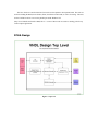
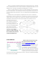
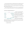
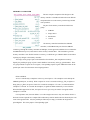
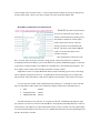
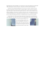
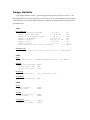
Mentor Graphics
2001 – 2002 Student Design Contest
CMOS Digital Camera Controller and
Frame Capture Device
By
Ryan Henderson
Oregon Institute of Technology
May 26, 2002
Project Abstract
Applications of digital imaging range from amateur photography to machine vision. This project
shows how a CMOS ‘Camera On a Chip’ image sensor can be used to build a high resolution web camera.
An I2C bus controls the image sensor, and the pixel data is buffered in SDRAM to be uploaded through the
parallel port to be displayed on a PC. The external hardware, FPGA design, and software application for
the camera will be described in this paper. Introduce myself
System Overview
Motivation for the design
For my senior project at Oregon Institute of Technology, I wanted something creative and flashy that
would challenge me as an engineer. The design needed to demonstrate my skills to prospective employers
in a job market that is centered on experience. The original idea behind the project was to place a camera
on a RC car. Then the car could be controlled much like a racing game from a computer.
Appropriate technology and implementation style
After much research on image sensors, the choice to use CMOS over CCD became clear. CCD
sensors typically offer superior image performance, CMOS sensors consume less power and are easier to
interface and control. (http://www.dalsa.com/markets/ccd_vs_cmos.asp) The Kodak KAC-1310 CMOS
sensor I chose integrates the analog to digital converters in the sensor, so all I/O ports to the sensor are
digital.
An FPGA was appropriate to control the sensor and buffer the data while minimizing component
count. I chose a XESS XSA-100 Spartan II development board to interface between the parallel port and
the image sensor. With 100k gates and 16Mb of storage, I had enough room and speed to implement
everything I needed.
Design methodology and why it methodology was chosen
After short consideration, VHDL was chosen over Verilog to implement the design. I prefer the strong
type checking of the language, and it also eased the integration of two third party cores into my design. The
general design mythology was to take large, already built components and assemble them together. Then I
implemented the glue code and controllers myself. The task was still daunting. Implementing someone
else’s code can be more difficult then writing it from scratch.
Satisfying the system requirements
My project specification calls for capture of high resolution images through the parallel port. In the
now completed design, the host PC can repeatedly capture an image from the camera and write it out to a
bitmap. The limited bandwidth of the parallel port restricts the video frame rate, but this was certainly
expected.
Uniqueness
Unique to other hardware senior projects at OIT for several years, I chose to use the Xilinx Spartan II
over an Altera 10k70. At about four times the speed and area, the XC2S100 on the Xess XSA-100
development board met the system requirements. This different choice of hardware also gave me the
opportunity to learn to use some new design tools.
The core of my project is a unique method to handle simultaneous asynchronous accesses to the
SDRAM. New pixel data is coming from the image sensor at a max rate of 12.5MHz. At the same time
the host PC could be reading the pixel data at a rate of approximately 150kHz. To make the SDRAM
appear dual-port, a specialized memory controller was design with a read and write asynchronous FIFOs
and access to the memory is controlled by a semaphore. With this solution, the SDRAM can be clocked
independent of the image sensor and parallel port.
To prevent an image from being updated before it is completely read out, the design keeps three
pictures in memory and pages through them. The newest image being read in is kept on one page. The last
complete image is kept on another page. The third page keeps the image the parallel port is reading out.
When new frames can be read in faster then they can be read out, this keeps each image intact.
Finally, because of the hardware limitation on the XSA-100 board, the parallel port is limited to nibble
mode. To improve bandwidth through the port and reduce noise, four bits are transferred on every clock
edge. Making the parallel port DDR doubled my data rate and reduced noise in the data stream.
Design Reuse and Testability
Design reuse was an important aspect of this project. Because of the flexibility of the Opencores I2C
controller, it was easily integrated into my design. Also, the use of this design isn’t limited to a camera. It
has the capability to capture data to memory at varying clock rates, and then upload the data for inspection.
Another application of this design would be a logic analyzer.
Large steps were taken to ensure testability. Sub-components were built and tested independently.
Internal block ram was used to test the dataflow through the design before the SDRAM was added.
HW/SW partitioning choices
While this was not a SOC design, there was still one HW/SW partitioning choice between the FPGA
design and the PC software. To capture color, image sensors use a Bayer RGB pattern where each pixel
only captures a single color. To fill in the missing color values for each pixel, one must use the adjacent
pixels, both horizontally and vertically. To implement this in hardware would require considerably more
design time and would actually inflate the size of the resulting image. The host PC software could easily
decode the color data with much less code.
List software used with software analysis to include feedback on problems, obstacles
encountered and workarounds.
A wide variety of software tools were used for this project. For the hardware design, tools were
needed for synthesis, simulation and place and route. Software design tools were needed to create the
image capture program.
Software & Etc
Hardware
•
Leonardo Spectrum
•
Visual C++ 6.0
•
ModelSim
•
Xess Tools 4.0
•
Xilinx ISE
•
Altera Max+plus II
The primary tool used for creating the hardware design was Leonardo Spectrum. The integrated place
and route feature allowed me to go from VHDL to bitgen with one push of a button. The RTL view
visualized my design and made finding problems easier. Leonardo’s buggy user interface was an annoying
obstacle to productivity. I also found that the Spartan 2 symbol IBUFG must not be buried in the design
hierarchy, or the tool will place another incompatible buffer in front of it and the Xilinx place and route
tool will fail.
Xilinx ISE was primary used through Leonardo spectrum to translate the design from electronic design
interchange format (EDIF) to a bitgen to program the FPGA. Some incompatibilities with bussed net
names in the EDIF file created problems. Some tools use < > and others use ( ). A simple find – replace
solved the problem. The Xilinx core generator tool was used for creating RAMs, FIFOs and other blocks.
Learning how to integrate these blocks into the simulation and synthesizable design took some searching.
Verifying the design using ModelSim proved invaluable. When the input patterns became more
complex and the time to go from VHDL to bitgen increased, the testbench was saved time. The difficult
part is making sure the testbench inputs match the actual design inputs.
For quick and dirty simulations, Altera’s Max+plus proved useful. The editable waveform simulation
tool made verifying a simple module easier and saved the time of writing a testbench.
Microsoft’s Visual C++ was used to create a camera controller application to run on the host pc. The
target platform for the application was Windows 2000, however access to the parallel port is restricted and
requires a driver. While considering how to write my own device driver, I found the Xess tools provided a
better option.
The Xess Tools are a small collection of accessories to the Spartan 2 development board. The tools are
useful for loading the RAM, clock divider, FPGA, and CPLD on the board, as well as for testing. The tools
use the Unified I/O driver to access the parallel port under Windows NT.
(http://www.bbdsoft.com/interface.html) The C++ source of these tools was used as a starting point for my
camera capture application.
FPGA Design
Figure ? Top Level
TOP LEVEL DESCRIPTION
The FPGA is the main controller of the camera, handling
data movement from the image sensor to the parallel port. At the
top level of the camera design, ports are arranged in the
following groups:
•
Image Sensor
•
SDRAM
•
Parallel Port and XSA-100 Misc. I/O
Image sensor ports connect to the development board with
the KAC-1310 sensor to provide timing, control and to read the
image data. SDRAM ports connect the address, bidirectional
data, and control signals on the XSA-100 board. Other signals
such as the clock and the parallel port connections are grouped in
XSA-100 misc. Some ports were added purely for testing, and
could be removed for a final design.
The top level design file primarily instantiates and connects sub components in the design. There are
also global buffers placed on clock input pins to help with fan-out and so they can be connected to delay
lock loops. Some of the component instantiations have generic mappings as well to define parameters for
the modules. Instantiated components at this level are:
•
clock_generation
•
KAC_data
•
LEDDecoder
•
pp_upload
•
Master_control_signal_genereator
•
ram_control
•
KAC_i2c
I2C CONTROLLER
The image sensor is controlled by the master control signal generator component by I2C, a two wire
bi-directional interface. A control module was created to
simplify this interface and constrain it to the specific
application. Forty 8-bit control registers in the image
sensor can be read and written to using a sequence of I2C
events as described in section 8 of the KAC-1310
datasheet.
The KAC_i2c component is implemented with the simple i2c controller from Open Cores. The author
of the core, Richard Herveille also wrote a sample state machine for reading data from a Dallas 1621, a I2C
temperature sensor. This sample was starting point for building the KAC_i2c controller.
The KAC_i2c module simplifies these sequences by providing a SRAM like interface that completely
hides the I2C implementation. The controlling entity needs only to setup the address, data, direction, and
assert the start signal to initiate a data transfer. The cycle is completed when the done handshaking signal
is asserted.
In addition to how to use this component, it’s important to know how it works. An internal state
machine handles two sequences, and an idle state. The machine stays in the idle state, and asserts safe idle
conditions, until an access is requested. Once a sequence starts, commands are issued in sequence to the
instantiated I2C controller. Because these states may take multiple clocks, the machine waits for an
acknowledge of the previous state
before continuing. The machine must
wait for the ack from the last state
before returning to the idle state. This
was a source of some dysfunctionality
while creating the state machine.
During the course of these states, the
input address and data values
alues are
transferred. The address and input data
bus are not latched, so they must remain
a constant value during the access.
CLOCK GENERATION
Board level deskew of the system clock was the
goal of the clock generation component. This is
described at http://www.xilinx.com/products
/spartan2/recipes/rec004.htm. The principle is to sync
the internal logic to the same clock that is seen by the
external SDRAM, accounting for PCB and buffer
delays. The clock signal is routed out of the Spartan II,
then back in through a dedicated clock pin. This delay
is sampled by a pair of delay lock loops which output
an internal clock which is phase shifted to decrease clock skew. If the clock is not deskewed, the SDRAM
will not function correctly at 50Mhz.
DLLs are also used as clock dividers. The 12.5Mhz clock for the KAC-1310 image sensor is divided
from the deskewed internal clock. The image sensor clock does not have a feedback, and is slightly
skewed, but at lower frequencies, clock skew is less of a problem. Alternatively, a simple counter could
have been used as a clock divider. However, using the DLLs to generate the slower frequency reduced the
50Mhz to 12.5Mhz clock edge delay by 50%.
Because it takes time for the DLLs to get lock, the board needs to be reset using the pushbutton after
power-up. The entire design could be modified, however, to use the locked signals and an internal reset.
ASYNCRONOUS DISTRIBUTED MEMORY FIFO
The FIFOs were produced using the Xilinx
Core Generator. By using a FIFO in each
component that needs access to the SDRAM, data
can be buffered if RAM access is blocked by
another component. Also, if SDRAM access
locations are bunched together, the memory will
respond faster then for accesses at addresses across
bank boundaries.
The write count output from the FIFO tells
roughly how full it is. The count is used for
signaling a need to dump, or receive more data. The FIFO is asynchronous, so it has a clock for putting
data in, and a clock for taking data out. The enable signals allow writing or reading only when needed.
They are highly preferred over gating the clock signals.
•
Wr_count vs rd_count
•
Distributed vs block ram
SDRAM CONTROLLER
Xess has provided an SDRAM controller that
makes the external 16Mx16 SDRAM look like simple
SRAM. It handles refresh and bank interleaving and
was available in a VHDL version. In its current state,
the SDRAM controller does not support burst mode
To provide pseudo dual port functionality with the
SDRAM, read and write FIFO’s were added to the
modules that read and write to the memory. The FIFOs
allow interleaved read and write operations to operate
efficiently and independent of each other. For instance,
if the parallel port needs to read from RAM at a rate of
100 kHz, it can pull data from a FIFO. When the FIFO
approaches almost empty, it can be filled with a burst
read from SDRAM at 50 MHz.
For testing, this component was replaced by
onboard block SelectRAM+ in the Spartan. Only 40k Bytes was available in the XC2S100. The block
RAM worked for testing, but wasn’t big enough to hold even a small picture.
The SDRAM controller provides an interface similar to the I2C controller. There are busses for data
in, data out, and address. When the read or write signal is asserted, the done signal goes low until the end
of the access. Valid data is read on the rising edge of the done signal. The controller can address 16Mbytes
and has a 16 bit wide data bus.
The controller was modified slightly from the original Xess version. All IBUFGs and DLLs were
moved to the top level, and the clock generation component. Also, a bug preventing correct setting of the
SDRAM’s mode register was fixed. For more information on this controller, please refer to Xess
documentation.
MEMORY CONTROLLER
The most complex component of the design was the
memory controller. It handles arbitration between different
components that access the memory, interleaving read and
write operations.
I/O ports for the memory controller divided in four
groups.
•
SDRAM
•
Image Sensor
•
Parallel Port
•
Control
The memory controller instantiates the SDRAM
controller, so all SDRAM side ports from the SDRAM
controller go through the memory controller. In hindsight, a better approach would have been to instantiate
the SDRAM at the top level, and connect it to the memory controller there. This would have given the
memory controller a more flexible interface to memory, so a different type of RAM could be used without
requiring any changes to the memory controller.
The image sensor group of ports controls dataflow from the KAC_data component to memory.
Equally, the parallel port group of ports controls dataflow from memory to the pp_upload module. These
two groups include a request for access signal, a corresponding response signal. Additional control for the
parallel port comes from the master control signal generator.
FIFO CONTROL
Access is controlled by a semaphore in the sem_control process. The semaphore can be held by the
SDRAM, parallel port, or nobody. When a request for access is asserted on either pp_fifo_need_data or
dump_data_req_KAC, the process checks if it can take the semaphore. If it can’t, it is blocked until the
semaphore is released. If it can take the semaphore, it signals the FIFO and memory to start a transfer.
When the FIFO approaches its limit, the request for access goes away, the transfer is stopped, and the
semaphore is released.
It is important to note, that each FIFO’s is set with enough extra room so they can continue while it is
blocked. The time required for a complete FIFO and memory transfer matches the time allotted by the extra
room in the opposite FIFO. Also, the parallel port FIFO may be empty, but the host PC might not be
uploading data. This is the purpose of the uploading signal.
ADDRESS GENERATION
The memory controller also manages the memory addresses for both data in and data out. The image
is kept in a simple linear array in memory, so the current address for a read or write is generated off a
binary up counter with some added set and reset logic. A separate address pointer is kept for the parallel
port and image sensor.
The signal addr_ptr_KAC is incremented for every write to the SDRAM. It is reset on the
start_new_frame signal from the KAC_data component. Additionally, the address pointer is prevented from
exceeding the maximum size of a picture and writing into the next frame. Memory paging is described in
the next section.
Handling of the parallel port address pointer, pp_addr_pointer is a little more complex. It is also
implemented with a counter, but is set and reset on values passed from the master control signal generator.
The pointer is set with the start address when start_upload is asserted, and it is clear when it reaches end
address or abort upload is asserted.
FRAME PAGING
Finally, the memory controller handles frame paging as well. Paging ensures that the picture being
uploaded does not update before it is completely read out. Otherwise, the bottom of the picture would be
more current then the top and moving objects would cause tearing in the image.
The current page is determined by the high three address bits, and there are three page registers.
When a page is swapped, the page registers exchange values. The SDRAM address for a read or write is
made up of the current ram page concatenated with the ram address pointer.
When a complete image has been read in, as indicated by the signal start_new_frame, ram_page_KAC
is swapped with ram_page_full. When a new parallel port upload is started, as indicated by the signal
start_upload, ram_page_full is swapped with pp_ram_page. In the event both start new frame and start
upload occur in the same clock, ram_page_KAC is swapped directly with pp_ram_page.
An engineering goal of the project is demonstrated here. The image read in and read out rates are
independent. Frames will be dumped, or duplicated to compensate for different transfer rates.
IMAGE SENSOR DATA READER
The image sensor data reader handles the timing generation, and data transfer from the image sensor.
A 64 deep by 16 bit wide asynchronous FIFO is used to buffer incoming data. Using the
init_cycle_complete signal, incoming data is ignored until startup operations have completed. Until this
signal is asserted by the master control signal
generator, no SDRAM writes are requested.
In this component, the master clock is sent to
the sensor and video sync and pixel data are
received. Internal connections go to the memory
controller to handle handshaking and data transfer
out of the FIFO.
A design decision was made to reduce the
color depth 8 bits per image sensor pixel. Two
successive pixels are placed together in the 16 bit
wide SDRAM to reduce bandwidth requirements.
The image sensor outputs a 8 bit color values at a
rate of approximately 12 MHz for a bandwidth of 7.5Mbytes/s.
Two state machines are used in this component. A simple state machine detects the rising edge of the
hclk signal to pack two 8 bit pixels together and stuff them into the FIFO. This state machine controls the
FIFO’s data in and write enable signals. Another short state machine controls the dump data request and
start new frame signals. When the FIFO approaches full or empty, dump data request is toggled
appropriately. Also, if a start of frame signal comes from the image sensor, the FIFO contents must be
emptied and then the start new frame signal must be asserted.
If the FIFO is not flushed on the start of a new frame, each frame will have part of the previous frame’s
data and the end of the current frame will be cut off. Flushing the FIFO must occur in under 550ns, the
time between the image sensor asserting start of frame and the first pixel of the new frame. The SDRAM
requires 50ns / write which allows for only 11 writes. The timing here is very tight, thus the FIFO is set to
request to dump when it reaches 8 entries. A more elegant solution would be to count pixels and generate
an end of frame signal. There is more time available to use between the EOF and the SOF.
MASTER CONTROL SIGNAL GENERATOR
The MCSG provides status and control
for top level components in the design. For
instance, commands from the parallel port are
decoded here, and then the control signals
initiate actions in the memory controller.
Startup procedures are also handled in the
MCSG. The image sensor and the SDRAM
require a reset and a time delay before
operation can begin.
This component has connections to the
KAC_i2c, KAC_data, the memory controller, and pp_upload. Interaction with the I2C controller is
accomplished with an 8-bit address, a pair of 8-bit data busses, and three handshaking signals. Connections
to the memory controller include a start address bus, end address bus, start and abort upload signals. Two
more outputs reset the image sensor and signal completion of startup routines.
Simplification of I2C to a simple SRAM like interface makes controlling register values in the image
sensor completely transparent at this level. As implemented, control of the image sensor is limited, but
fully functional. More functionality could easily be added to take advantage of the features in the sensor.
A several step state machine reads commands from the parallel port. Commands are 6-bits wide and
three are implemented. More details can be found in the diagram “Parallel Port Command Protocol.”
•
NOP
000000
•
STARTUPLOAD
000001
•
ABORTUPLOAD
000010
The NOP command is a safe idle state, so no signals are affected. STARTUPLOAD begins an eight
step sequence to read in two 24 bit start and end addresses, the beginning and ending addresses of where to
read in memory. The addresses are registered and passed to the memory controller. The start_upload signal
is asserted when both addresses have been received. ABORTUPLOAD asserts the abort upload signal, also
passed to the memory controller.
The image sensor’s reset or init signal requires 1ms asserted, then 1ms de-asserted before the sensor
can begin. Also, the SDRAM requires 200us of startup time. The init_cycle_complete signal indicates that
startup routines have completed.
PARALLEL PORT INTERFACE
An important component for sending the image, debugging and system control is the parallel port. The
pp_upload component buffers data from the SDRAM
in a FIFO to send through the parallel port to the
image capture program on the host PC. Commands
are also received and passed onto the MCSG.
The port operates in nibble mode with four bits
for upload and eight for download. On the XSA-100
prototype board, the high download bit is physically
tied to the Spartan program pin. This bit is pulled
low to reconfigure the FPGA, otherwise it must be held high. The lowest download bit, always driven by
the host PC, is used to clock data through the port. This limits the download data width to six bits.
To increase upstream bandwidth through the port, nibbles are uploaded on both edges of the parallel
port clock. This design decision doubled bandwidth through the port, but added some complexity. The 16
bit FIFO output is broken into four pieces which are selected by the current edge of the parallel port clock
and a toggle bit.
Interaction with the memory controller to feed the FIFO is similar to what’s implemented in
KAC_data. When the FIFO approaches empty, it signals a request for data to the memory controller. The
memory controller will respond with the wr_en signal and will fill the FIFO until need_data is de-asserted.
The parallel port upload component de-asserts need_data when the FIFO approaches full. Because there is
more then one clock delay between the de-asserting of need_data and wr_en, the FIFO’s almost full signal
is not used.
ACCESSORY COMPENTS
Several self explanatory accessory components are also used. These are sprinkled throughout the
design where needed. LED Decoder converts 4 bit binary for display on a 7 segment. Oneshot uses a state
machine to output a one clock period long pulse on the positive edge of the input signal. The component ms
delay asserts a done signal 1ms after start is asserted. Signal debounce stops false triggering on a signal
with dirty edges. The number of clocks to wait for the bounces to stop is generic. Clock divider is a
replacement for the clock generation component, without the DLLs.
•
LED Decoder
•
Oneshot
•
ms Delay
•
Signal Debounce
•
Clock Divider
Verification and Simulation
A challenge equal to creating a design itself is proving that the design works as expected. For my
digital camera project, verification was done by simulation and in hardware testing. Both methods require
extra design considerations and overhead, but in turn can simplify the design process.
SIMULATION
Test benches were written to verify the design using ModelSim. The testbench exercises the design at
the top level simulating the parallel port and image sensor interactions. The advantage of simulation is all
intermediate signals in the design can be viewed. For verifying the memory arbitrator and FIFO
interactions, this became imperative. The disadvantage of simulating this design was ensuring simulated
input matched the actual inputs to the design when it was placed in hardware. An inaccurate simulation
may insist a bad design is actually functioning correctly.
Timescale issues and missing models made simulation difficult. The design was clocked at 50Mhz and
to receive an entire picture through the parallel port required 10s. The computational time to get 10s of
simulation became unwieldy. In response, the parallel port was simulated as 100x faster which effected the
memory access timings. Also, I didn’t have a model for the SDRAM for simulation, so once it was verified
in hardware, correct functionality was assumed in simulation. SDRAM accesses were observed at the
SDRAM controller interface rather then the SDRAM to hardware interface.
To simulate the Xilinx Coregen FIFOs and block RAMs, some libraries had to be added in modelsim.
The Xilinx Libraries Aid TCL script (Xilinx_lib_4.tcl) was used to add the unisim and XilinxCoreLib
libraries.
IN HARDWARE
Testing in hardware gives definitive decision if this design works or not. When the design is placed in
hardware, pins can be probed and real delays can be measured. A logic analyzer and oscilloscope was
used, as well as DIP switches and LEDs. Also, the parallel port connect and image capture software was
used for debugging. Testing results could be stored to memory, transferred, and then written to a file for
examination on the host PC. The design has similarities to a logic analyzer and this was taken advantage
of.
The goal of the project was not merely the design, but a working camera. To meet this goal, a small
prototype board was built to house the image sensor. Voltage regulators, capacitors, header pins and a
socket for the sensor were placed on the board following the sample circuit in KAC-1310 datasheet. The
header pins on this board were then connected with wire wrap to the XSA-100 development board. Signal
connections are listed in the FPGA pin-out description.
The most important in hardware testing was the testing the FIFOs and memory controller. Transfer of
data from the image sensor to the host PC is a four step process. Working backwards through each of these
steps, input data was simulated using a simple binary up counter. For instance, to verify the parallel port
link between the hardware and the host PC, a counter was placed to simulate the output of the parallel port
FIFO. Problems with byte order, FIFO overflow or FIFO underflow could be found here. This testing was
performed at the following four areas:
•
Output of parallel port FIFO
•
Output of SDRAM
•
Input to SDRAM
•
Input to image sensor FIFO
Use of Dallas temperature sensor to test I2C
Problems and Workarounds
Indeed there were many problems that put sections of the project on hold. Most often the solution was
simple yet novel.
False triggering on the parallel port clock caused by noise through the parallel port cable and signal
bounce was one simple problem. This was found by reading the value of a counter incrementing off the
parallel port. Correct clocking would cause an incrementing sequence to be written to the binary data file.
When the clock would false trigger, the sequence in the file would skip several numbers at a time. This
was solved with a debounce circuit. The solution was easy; finding the problem of the errors was more
difficult.
Some problems were not related to hardware, but the synthesis or place and route tools. I found that
global input buffers must be placed on the top level of the design or Leonardo Spectrum will place an
illegal input buffer in front of the IBUFG. Also, fanout grew too large on the parallel port clock signal and
I had to manually place a buffer on the signal. Usually, the tool will insert a buffer automatically.
Finally, there is the problem that stumped me for four weeks to be solved in 5 minutes with a pog.
According to the datasheet, and email responses from Robert McKeever and Grace Pigott at Kodak, the
image sensor begins to output video and sync signals on power up. However, when I would power it up,
nothing would happen, in fact the device would not even draw any current. I tested the pins at the socket
contacts and found that all power, ground and necessary signals were correct. I could not test the pins on
the CLCC image sensor package because they were buried in the socket. This led me to the problem.
I found out the CLCC socket I had was made to place the IC in upside down, not real beneficial for
camera applications. The contacts in the socket were not touching all the recessed contacts on the image
sensor because the glass lid hung over too
far, as seen by the picture on the left. The
picture on the right shows where pins were
making contact. The contacts in the socket
were shaped so that raising the sensor about
1mm allowed all connects to make contact.
Design statistics
A good design functions correctly. A better design functions correctly with fewer resources. The
Xilinx Spartan 2 was an excellent target device for the project. Its size, speed and more then outweigh the
extra complexity over an Altera 10K70. Following is a summary of post place and route design statistics
optimized for area.
AREA
FPGA Utilization
Number of External GCLKIOBs
3 out of 4
Number of External IOBs
77 out of 92
Number of LOCed External IOBs
77 out of 77
Number of BLOCKRAMs
1 out of 10
Number of SLICEs
478 out of 1200
Number of DLLs
2 out of 4
Number of GCLKs
3 out of 4
Total equivalent gate count for design:
75%
83%
100%
10%
39%
50%
75%
46,685
SDRAM Useage
3 Frames * 1280 Pixels * 1024 Lines * 8 bits = 3,840 Mbytes
SPEED
FPGA
Minimum period:
15.088ns (Maximum frequency:
SDRAM
Operating frequency: 50Mhz
Average write time: 50ns
Average read time:
100ns
Parallel Port
Upload bandwidth:
100 - 150k bytes / sec
Image Sensor
Operating frequency: 5Mhz
POWER
FPGA
Total current:
Total power:
130mA
320mW
SDRAM
Operating current:
Total power:
120mA
400mW
Image Sensor
Total current:
Power at 13.5Mhz:
120mA
400mW
66.278MHz)
Summary
For a senior project requirement at Oregon Institute of Technology, I created a digital camera. The
camera was built using the KAC-1310 CMOS image sensor from Kodak and the XSA-100 FPGA
development board from Xess. Control of the camera was written in VHDL, synthesized with Leonardo
Spectrum and translated to a bitgen with Xilinx ISE. The design was verified in hardware and with
ModelSim. The image is captured from the camera to the host PC with a small windows application.
The VHDL design placed in the Spartan 2 FPGA on the development board has several functions. The
design controls the camera IC by I2C and transfers and image stream from the camera through buffers to
SDRAM. Commands are received from the host PC through the parallel port to read an image. The image
is then transferred from the SDRAM, through more buffers and out the parallel port.
The design is unique in that it provides a simulated dual port interface to SDRAM. The image sensor
can write to memory while the host PC is reading from it. Images are stored in pages to preserve image
integrity. All pixels in a received image are from a single image capture by the sensor. The use of a Xilinx
FPGA makes this project unique among other OIT projects.
References
comp.arch.fpga
comp.lang.vhdl
XSBoard User Group [email protected]
Peter J. Ashenden, “The designers guide to VHDL.” Morgan Kaufmann Publishers, 1995.
Qualis Design Corporation, VHDL QUICK REFERENCE CARD. http://www.qualis.com
Photobit, PB-MV13 Product Specification, www.photobit.com
Photobit. PB-0300 Mini-EPPI Camera Development System User Manual, www.photobit.com
Agilent, Image Processing Chip HDCP-2010 (YUV/JPEG Output) Product Brief.
www.semiconductor.agilent.com
Agilent, HDCS-1020, HDCS-2020 CMOS Image Sensors Data Sheet
www.semiconductor.agilent.com
Agilent, HDCP-2000 Image Processor Data Sheet www.semiconductor.agilent.com
Agilent, An Image Processing Chip for the HDCS Family of CMOS Image Sensors.
www.semiconductor.agilent.com
D. Vanden Bout, Xess Corp. XSA SDRAM Controller an-09260-sdramcntl.pdf www.xess.com
D. Vanden Bout, Xess Corp. XSA Parallel Port Interface an-111601-xsapport.pdf www.xess.com
D. Vanden Bout, Xess Corp. XSA Flash Programming and SpartanII Configuration
an-111701-xsaflash.pdf www.xess.com
Atmel, 1-megabit (128K x 8) 5-volt Only Flash Memory AT49F001 www.atmel.com
Xess Corp, Introduction to WebPACK 4.1 for FPGAs. www.xess.com
Xess Corp, XSA Board V1.0 User Manual www.xess.com
Analog Devices, CMOS 80 MHz, Triple 8-Bit Video DAC ADV7120.pdf. www.analog.com
Charles Poynton, Frequently Asked Questions about Color. www.inforamp.net/~poynton
Tom Hill, Exemplar Logic. Inferring Virtex Block RAM with Leonardo Spectrum Leonardo Spectrum
www.exemplar.com/Xilinx Datasheets
Hynix Semiconductor. HV7131E CMOS IMAGE SENSOR System IC SBU With 8-bit ADC
www.hynix.com
Hynix Semiconductor. HY57V281620A 4 Banks x 2M x 16bits Synchronous DRAM. Datasheet
www.hynix.com
Hynix Semiconductor. SDRAM Device Operation www.hynix.com
Hynix Semiconductor. SDRAM Timing Diagrams www.hynix.com
Elpida Memory, How to use SDRAM User’s Manual E0123N10I. http://www.elpida.com
Richard Herveille, Opencores.org I2C-Master Core Specification www.opencores.org
Zoran. ZR36060 INTEGRATED JPEG CODEC. www.zoran.com
Eastman Kodak Company KAC – 1310 1280 x 1024 SXGA CMOS Image Sensor.
http://www.kodak.com/US/en/digital/ccd/sensorsMain.shtml
Eastman Kodak Company Kodak KAC-ES001-A Evaluation System.
http://www.kodak.com/US/en/digital/ccd/sensorsMain.shtml
Motorola. Color SXGA Digital Image Sensor 1280 x 1024 pixel progressive scan solid state image sensor
with integrated CDS/PGA/ADC, digital programming, control, timing, and pixel correction features.
e-www.motorola.com
Motorola, Optics: Sensor – Lens Selection AN1929.pdf e-www.motorola.com
Motorola , White Balance and Color Correction in Digital Cameras AN1904 e-www.motorola.com
Motorola, The Roadrunner Modular digital still camera reference design. AN1928.ppdf
e-www.motorola.com
National Semiconductor, LM9627 Color CMOS Image Sensor VGA 30 FPS. www.national.com
Plastronics, LCC Socket 48-Lead 0.040 Square. P2048S. Mechanical Drawing. www.locknest.com
Xilinx, XC9572XL High Performance CPLDPreliminary Product Specification DS057. www.xilinx.com
Xilinx, CoolRunner XPLA3 I2C Bus Controller Implementation. XAPP333. www.xilinx.com
Xilinx, Synthesizable High Performance SDRAM Controller XAPP134 www.xilinx.com
Robert McKeever, [email protected] Eastman Kodak Company. Email correspondence.
Nicolas Matringe [email protected] comp.arch.fpga Email correspondence
Charles Petzold, Programming Windows. Microsoft Press. 1999