1
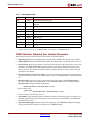
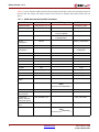
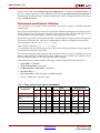
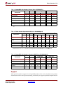
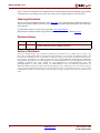
0 Binary Counter v11.0 DS215 April 24, 2009 0 Introduction Product Specification 0 Pinout X-Ref Target - Figure 1 The Xilinx® LogiCORE™ IP Binary Counter core provides LUT and single XtremeDSP™ slice counter implementations. The Binary Counter is used to create up counters, down counters, and up/down counters with outputs of up to 256-bits wide. Support is provided for one threshold signal that can be programmed to become active when the counter reaches a user defined count. The upper limit of the count is user programmable and the counter’s increment value can be user defined. When the counter reaches terminal count or the count to value, the next count will be zero. Q SCLR CLK CE LOAD L C_IN SSET* Features THRESH0 UP SINIT* Drop-in module for Virtex®-6, Virtex-5, Virtex-4, Spartan®-6, Spartan-3/XA, Spartan-3E/XA, Spartan-3A/AN/3A DSP/XA FPGAs Backwards compatible with version 9.1 Generates up, down, and up/down counters Supports fabric implementation counters ranging from 1 to 256 bits wide Supports DSP48 implementation counters ranging from 1 to 36, or 48 bits wide (varies with device family) Pipelining added for maximal speed performance Predictive detection used for threshold and terminal count detection Optional synchronous set and synchronous init capability for legacy fabric implementations Optional user programmable threshold outputs Optional clock enable and synchronous clear Counter increment value can be user defined User-programmable count limit For use with Xilinx CORE Generator™ and Xilinx System Generator™ v11.1 or later C_IN *Fabric implementation in legacy mode only Figure 1: Core Symbol Signal names for the core symbol are shown in Figure 1 and described in Table 1. Note that Figure 1 shows the SSET and SINIT pins which appear only on legacy fabric implementations. The fabric legacy mode has been provided to preserve backwards compatibility but allow performance to be improved. This is where Implement using = Fabric, Latency = 1 and FB_Latency = 0. © 2006-2009 Xilinx, Inc. Xilinx, Inc. XILINX, the Xilinx logo, Virtex, Spartan, ISE and other designated brands included herein are trademarks of Xilinx in the United States and other countries. All other trademarks are the property of their respective owners. DS215 April 24, 2009 Product Specification www.xilinx.com 1 Binary Counter v11.0 Table 1: Core Signal Pinout Signal Direction Description CLK Input Clock. Rising edge clock signal UP Input Controls the count direction on an up/down counter. Counts up when high, down when low CE Input Active high Clock Enable SCLR Input Synchronous Clear: forces the output to a low state when driven high THRESH0 Output User-programmable active high threshold signal Q[N:0] Output Output L[N:0] Input Load data port LOAD Input Load control signal SSET1 Input Synchronous Set: forces the output to a high state when driven high SINIT1 Input Synchronous Initialize: forces the outputs to a user defined state when driven high 1. Available only when in fabric legacy mode: Implement using = Fabric, Latency = 1, and Feedback Latency = 0 CORE Generator Graphical User Interface Parameters The CORE generator GUI parameters for this module are described below: Implement using: Sets the implementation type to Fabric or DSP48. The default value is Fabric. Output Width: Specifies the width of the counter. The valid range is 1 to 256. Default value is 16. Restrict Count: When this parameter is true the counter will only count up (or down) to the value specified in the Final Count Value parameter. When it is false the counter will count up to the maximum value that can be represented using the specified output width.The default is for no count restriction. This option is mutually exclusive with the up/down counter option and with synchronous set controls. Final Count Value: When Restrict Count = true, this parameter specifies the hex representation of the upper limit of the counter. The valid range for values is 1 to 2Output Width - 2. The default value is 1. Increment Value: Specifies in hex the increment value of the counter. When Restrict Count is false, the valid range is 1 to 2Output Width - 1. When Restrict Count is true the valid settings for Increment Value are governed by the equation: Final Count Value / Increment Value = Integer for up counters, and: 2Output Width - Final Count Value / Increment Value = Integer for down counters. The default value is 1. 2 Count Mode: This parameter specifies whether the counter will count up, down, or will have its direction specified on the UP pin (up/down). The valid values are UP, DOWN, and UPDOWN. The default value is UP. Sync Threshold Output: When this parameter equals true, the THRESH0 combinatorial output will be generated. The default is to not generate a THRESH0 output. www.xilinx.com DS215 April 24, 2009 Product Specification Binary Counter v11.0 Threshold Value: Specifies the value at which the THRESH0 value will be activated as a hex value. The valid range is 0 to Final Count Value for restricted counters, and 0 to 2Output Width - 1 for unrestricted counters. The default value is 1. Loadable: Activating the LOAD pin (Loadable = true) allows the value on the L[N:0] input port to pass through the logic and be loaded into the output register on the next active clock edge. The default is for no LOAD pin to be generated (Loadable = false). See the section, "Use of LOAD" for more information. Load Sense: Specifies Active_High or Active _Low LOAD pin. The default value is Active_High. CE: When set to true, the module is generated with a clock enable input. The default setting is true. Power on Reset Init Value: Specifies in hex the value the Q register will initialize to during power-up reset. Valid values are 0 up to 2Output Width - 1. The default value is 0. Synchronous Clear (SCLR): Specifies if an SCLR pin is to be included. Valid values are true or false; default is false. SSET: Specifies if an SSET pin is to be included. SSET pin is not valid in DSP48 implementations. See Sync Set and Clear (Reset) Priority for SCLR/SSET priorities. Valid values are true or false; default is false. SINIT: Specifies if an SINIT pin is to be included which, when asserted, will synchronously set the S value to the value defined by Init Value. Note that if SINIT is present, then neither SSET nor SCLR may be present. Valid values are true or false, default is false. SINIT pin is not valid in DSP48 implementations. Init Value: Specifies in hex the value the S register will initialize to when SINIT is asserted. Valid values are 0 up to 2Output Width - 1 for unrestricted counters, and 0 up to Final Count Value for restricted counters. Ignored if SINIT is false. The default setting is false. Synchronous Controls and Clock Enable (CE) Priority: This parameter controls whether or not the SCLR, (and if fabric: SSET and SINIT) input is qualified by CE. When set to Sync_Overrides_CE, the synchronous control overrides the CE signal. When set to CE_Overrides_Sync, SCLR has an effect only when CE is high. This parameter is ignored unless Clock Enable is true. Note that on the fabric primitives, the SCLR and SSET controls override CE, so choosing CE_Overrides_Sync will generally result in extra logic. The default is Sync_Overrides_CE. Sync Set and Clear (Reset) Priority: Controls the relative priority of SCLR and SSET. When set to Reset_Overrides_Set, SCLR overrides SSET. The default is Reset_Overrides_Set, as this is the way the primitives are arranged. Making SSET take priority requires extra logic. Latency Configuration: Automatic or Manual; Automatic sets optimal latency for maximum speed; Manual allows user to set Latency to one of the allowed values. The default value is Manual. Latency: Value used for latency when Latency Configuration is set to Manual: 1 to 32; See the section, "Pipelined Operation" for more information. The default value is 1. Feedback Latency Configuration: Automatic or Manual; Automatic sets optimal feedback latency for maximum speed; Manual allows user to set Feedback Latency to one of the allowed values. The default value is Manual. Feedback Latency: Value used for latency when Feedback Latency Configuration is set to Manual: 0 to 4; See the section, "Pipelined Operation" for more information. The default value is 0. DS215 April 24, 2009 Product Specification www.xilinx.com 3 Binary Counter v11.0 Table 2 is a cross-reference table from the GUI parameters listed above to the XCO parameter names in the XCO file. The ranges and default values are also shown to facilitate data retrieval from the text above. Table 2: CORE Generator GUI and XCO Parameters GUI Name Default Value Valid Range XCO Parameter c_counter_binary_v11_0 .. Component_Name Fabric .. Implementation Output Width 16 1..256 (fabric) 1..36 or 48 (DSP48) Output_Width Increment Value1 1 unrestricted: 1..2(Output Width)- 1 Increment_Value Manual .. Latency_Configuration 1 1..32 Latency Feedback Latency Configuration Manual .. Fb_Latency_ Configuration Feedback Latency 0 0..4 Fb_Latency Clock Enable false .. CE Synchronous Clear false .. SCLR Synchronous Set false .. SSET Synchronous Init false .. SINIT Loadable false .. Load Active_High .. Load_Sense false .. Restrict_Count 1 1..2(Output Width)- 2 Final_Count_Value Sync Threshold Output Active_Low .. Sync_Threshold_Output Threshold Value 1 restricted: 0..(Final Count Value) unrestricted: 0..2(Output Width)- 1 Threshold_Value UP UP, DOWN, UPDOWN Count_Mode Sync Set and Clear (Reset) Priority Reset_Overrides_Set .. Sync_Ctrl_Priority Synchronous Controls and Clock Enable (CE) Priority Sync_Overrides_CE .. Sync_CE_Priority Power on Reset Init Value 0 0..2(Output Width)- 1 AINIT_Value Sync INIT value 0 restricted: 0..(Final Count Value) unrestricted: 0..2(Output Width)- 1 SINIT_Value Component Name Implement using Latency Configuration Latency Load Sense Restrict Count Final Count Value Count Mode 1. See details above for explanation of Increment Value range when Restrict Count is true. 4 www.xilinx.com DS215 April 24, 2009 Product Specification Binary Counter v11.0 Core Use through CORE Generator The CORE Generator GUI performs error-checking on all input parameters. Resource estimation and latency information are also available. Several files are produced when a core is generated, and customized instantiation templates for Verilog and VHDL design flows are provided in the .veo and .vho files, respectively. For detailed instructions, see the CORE Generator software documentation. Simulation Models The core has a number of options for simulation models: VHDL behavioral model in the xilinxcorelib library VHDL unisim structural model Verilog unisim structural model Xilinx recommends that simulations utilizing unisim-based structural models are run using a resolution of 1 ps. Some Xilinx library components require a 1 ps resolution to work properly in either functional or timing simulation. The unisim-based structural models might produce incorrect results if simulation with a resolution other than 1 ps. See the “Register Transfer Level (RTL) Simulation Using Xilinx Libraries” section in Synthesis and Simulation Design Guide for more information. This document is part of the ISE® Software Manuals set available at www.xilinx.com/support/software_manuals.htm. Core Use through System Generator The Binary Counter core is available through Xilinx System Generator, a DSP design tool that enables the use of The Mathworks® model-based design environment Simulink for FPGA design. The Binary Counter core is one of the DSP building blocks provided in the Xilinx DSP blockset for Simulink. The Binary Counter core can be found in the Xilinx Blockset in the Math section. The block is called “Counter”. See the System Generator User Manual for more information. Migrating to Binary Counter v11.0 from Earlier Versions Updating from Binary Counter v9.0 and later The CORE Generator core update feature may be used to update an existing Binary Counter XCO file to version 11.0 of the core. The core may then be regenerated to create a new netlist. See the CORE Generator documentation for more information on this feature. Updating from versions prior to binary Counter v9.0 It is not currently possible to automatically update versions of the Binary Counter core prior to v9.0. Xilinx recommends that customers use the Binary Counter v11.0 GUI to customize a new core. Note that some features and configurations may be unavailable in Binary Counter v11.0. Also, some port names may differ between versions. Priorities of Input Signals SCLR/SSET. The priority of SCLR versus SSET can be configured using the Sync Set and Clear (Reset) Priority parameter as described above. LOAD. The synchronous controls (SCLR, SSET, SINIT) take priority over LOAD. DS215 April 24, 2009 Product Specification www.xilinx.com 5 Binary Counter v11.0 Note that if SCLR, SSET, SINIT or LOAD are affected by CE (specified in the Synchronous Controls and Clock Enable (CE) Priority parameter), a low CE value causes these signals to be ignored. For example, if SCLR is affected by CE, then with a low CE, LOAD appears to override SCLR (contrary to what was initially presented above. However, because SCLR has no effect when CE is low, this is the correct affect). Discussion of Restricted Counters The restricted counter option is implemented using an equality test rather than a greater-than-or-equal-to test. This means that if the counter somehow manages to skip the Final Count Value value, it will keep going. As such, there are restrictions on allowable parameters for restricted counters: Count Mode cannot be UPDOWN. SSET must be false. Additionally, there are restrictions added by pipelining as discussed in "Pipelined Operation" and there are further restrictions that differ for up counters and down counters. Up Counters Restricted up counters count up by Increment Value until Q = Final Count Value. The clock cycle after Q = Final Count Value, the counter resets to 0. There are two basic restrictions: Final Count Value must be an integer multiple of Increment Value Increment Value must be less than or equal to Final Count Value In addition, the values listed below must satisfy the following formulae: <value> IncrementValue = Integer <value> Final Count Value Init Value, if SINIT is used AINIT Value for power-on reset Any value loaded on the L data port. Down Counters Restricted down counters count down by Increment Value until Q = Final Count Value. The clock cycle after Q = Final Count Value, the counter resets to 0, and the counter continues counting down (wrapping around). There are two basic restrictions: Output Width 2 – Final Count Value must be an integer multiple of Increment Value Output Width Increment Value must be less than or equal to 2 – Final Count Value In addition, the values listed below must satisfy the following formulae: Output Width 2 – <value> Increment Value = Integer either <value> Final Count Value or <value> = 0 6 Init Value, if SINIT is used AINIT Value for power-on reset www.xilinx.com DS215 April 24, 2009 Product Specification Binary Counter v11.0 Any value loaded on the L data port. Use of LOAD The Counter core can check on instantiation for sensible Init Value and power-on reset value, but it cannot check the data loaded on the L data port. Because of this, erroneous values loaded will cause unexpected behavior in the counter. For example, if a counter is given Final Count Value = 8 and Increment Value = 2, loading in 3 will cause it to count the odd numbers and completely miss the limit value. Load Support The load operation in an XtremeDSP™ Slice (DSP48) requires DSP48 opmode control. The opmode control affects some of the same bits as are controlled to allow the terminal count reset feature. For the bits affected, external gating is required. This either impacts performance or requires an additional layer of latency in the feedback path. An extra layer of latency in the load path requires external registers for the D port of DSP48A and on the C register used for the Increment Value. Despite being a constant, the Increment Value is registered so that the recover from SCLR latency matches the LOAD latency. The latency of the counter for the DSP48 implementation is therefore width dependant and varies as a function of Restrict Count, Loadable, Load Sense, Output Width and the device family chosen. The Load Enable in v9.0 and earlier has been dropped. LOAD will always be subject to CE (if present). In DSP48, the A:B concatenated port width is 36 bits.. Hence output width is limited to 36 bits for the Virtex 4 cases with LOAD. Moreover, the detection of the terminal count has been further improved in version 11.0, but to maintain backward-compatible behavior, the improved detection cannot be used when the counter is loadable. Therefore it is strongly recommended that LOAD is not used with restricted counters; if such functionality is required, use external logic to create a greater-than-or-equal-to test rather than an equal-to test, or make sure the counter is simple (count by 1) and that a value is never loaded beyond Final Count Value. Pipelined Operation Pipelining the terminal count detection requires that the actual value detected is the terminal count value minus some multiple of the Increment Value value where the multiple is determined by the full cycle latency. This adds further restrictions to the valid combinations of Increment Value and Final Count Value. A run-time assertion (warning) will flag if a value is loaded which would cause the actual terminal count value to be missed. To allow for high performance, four new parameters have been added to the core: Latency Configuration, Latency, Feedback Latency Configuration, and Feedback Latency. The first two describe the number of cycles the core will take to recover from SCLR or from a LOAD value since it is the number of registers in the forward data path. When Latency Configuration is set to Manual, Latency can be set to a specific number for specific latency. By setting Latency Configuration to Automatic, the latency for maximal performance will be calculated internally and used in place of Latency. Maximal performance is defined as an operating frequency greater than or equal to the nominal operating speed of a fully pipelined XtremeDSP slice. For Virtex4-10 this is 400MHz. For Virtex5-1 this is 450MHz. For Spartan3ADSP this is 250MHz. This is achieved by splitting the carry-chain of the main count operation into splices and pipelining. The number of splices required is a function of the counter bit width and the family in question. Feedback Latency Configuration and Feedback Latency refer to the latency in the terminal count feedback circuit and hence apply only to restricted counters. The total amount of latency gives the number of cycles by which the terminal count detection must predict the DS215 April 24, 2009 Product Specification www.xilinx.com 7 Binary Counter v11.0 terminal count value. When Feedback Latency Configuration is set to Manual, Feedback Latency can be set to a specific number for specific feedback latency. By setting Feedback Latency Configuration to Automatic, the feedback latency for maximal performance will be calculated internally and used in place of Feedback Latency. Performance and Resource Utilization Table 3 through Table 6 provide Counter performance and resource usage for a number of different configurations. The maximum clock frequency results were obtained by double-registering input and output ports to reduce dependence on I/O placement. The inner level of registers used a separate clock signal to measure the path from the input registers to the first output register through the core. The resource usage results do not include the above "characterization wrapper" registers and represent the true logic used by the core. LUT counts include SRL16s or SRL32s (according to device family). The map options used were: “map -pr b -ol high.“ The par options used were: “par -t 1 -ol high.” Clock frequency does not take clock jitter into account and should be derated by an amount appropriate to the clock source jitter specification. The maximum achievable clock frequency and the resource counts may also be affected by other tool options, additional logic in the FPGA device, using a different version of Xilinx tools, and other factors. The Xilinx Xplorer™ script can be used to find the optimal settings. All characterization was done using the following parameter settings unless otherwise noted: Count Mode = UPDOWN Latency Configuration = Automatic Feedback Latency Configuration = Automatic Increment Value = 1 Final Count Value = 4B2A189 (fabric) and AF0C3 (DSP48) all else = default unless otherwise noted Table 3: Fabric Counter: Virtex-5 (Part = XC5VSX50T-1) Description Load1 Restrict Count2 Sml Med Lrg Sml Med Lrg Sml Med Lrg Output Width 18 47 200 18 47 200 18 47 200 Max Clock Frequency (MHz) 450 433 353 444 407 316 452 450 378 LUT6-FF pairs 19 92 437 19 137 770 25 129 462 LUTs 19 71 389 19 71 529 22 76 418 Flip-flops 18 86 419 18 132 751 25 128 454 DSP48Es 0 0 0 0 0 0 0 0 0 1. Load test cases are for a counter with the following parameter values: Loadable = true, Load Sense = Active_High. 2. Restrict Count test cases are for a counter with the following parameter values: Restrict Count = true, Count Mode = UP. 8 www.xilinx.com DS215 April 24, 2009 Product Specification Binary Counter v11.0 Table 4: XtremeDSP slice Counter: Virtex-5 (Part = XC5VSX50T-1) Load High1 Description Load Low Sml Med Sml Med Sml Med Output Width 35 48 35 48 35 48 Max Clock Frequency (MHz) 450 450 450 450 450 450 LUT6-FF pairs 7 43 45 94 45 94 LUTs 7 10 9 12 9 12 Flip-flops 7 43 45 94 45 94 DSP48Es 1 1 1 1 1 1 1. Load test cases are for a counter with the following parameter values: Loadable = true. ALL DSP48 tests have Restrict Count = true. Table 5: Fabric Counter: Spartan-3A DSP (Part = XC3SD3400A-4) Description Load1 Restrict Count2 Sml Med Lrg Sml Med Lrg Sml Med Lrg Output Width 18 47 200 18 47 200 18 47 200 Max Clock Frequency (MHz) 248 205 193 217 197 187 261 243 230 LUTs 49 94 512 88 165 937 56 104 554 Flip-flops 36 102 464 54 172 840 57 123 549 DSP48As 0 0 0 0 0 0 0 0 0 1. Load test cases are for a counter with the following parameter values: Load = true, Load Sense = Active_High. 2. Restrict Count test cases are for a counter with the following parameter values: Restrict Count = true, Count Mode = UP. Table 6: XtremeDSP slice Counter: Spartan-3A DSP (Part = XC3SD3400A-4) Description Load High1 Load Low Sml Med Sml Med Sml Med Output Width 35 48 35 48 35 48 Max Clock Frequency (MHz) 169 170 169 170 169 170 LUTs 11 16 13 18 13 18 Flip-flops 21 21 59 72 59 72 DSP48As 1 1 1 1 1 1 1. Load test cases are for a counter with the following parameter values: Load = true. ALL DSP48 tests have Restrict Count = true. Support Xilinx provides technical support for this LogiCORE product when used as described in the product documentation. Xilinx cannot guarantee timing, functionality, or support of product if implemented in DS215 April 24, 2009 Product Specification www.xilinx.com 9 Binary Counter v11.0 devices that are not defined in the documentation, if customized beyond that allowed in the product documentation, or if changes are made to any section of the design labeled DO NOT MODIFY. Ordering Information This core may be downloaded from the Xilinx IP Center for use with the Xilinx CORE Generator v11.1 and later. The Xilinx CORE Generator system is shipped with Xilinx ISE Foundation™ Series Development software. To order Xilinx software, contact your local Xilinx sales representative. Information on additional Xilinx LogiCORE modules is available on the Xilinx IP Center. Revision History Date Version Description of Revisions 4/24/2009 11.0 Initial release of c_counter_binary core with XtremeDSP slice implementations, and new family support for Virtex-6 and Spartan-6 devices Notice of Disclaimer Xilinx is providing this design, code, or information (collectively, the “Information”) to you “AS-IS” with no warranty of any kind, express or implied. Xilinx makes no representation that the Information, or any particular implementation thereof, is free from any claims of infringement. You are responsible for obtaining any rights you may require for any implementation based on the Information. All specifications are subject to change without notice. XILINX EXPRESSLY DISCLAIMS ANY WARRANTY WHATSOEVER WITH RESPECT TO THE ADEQUACY OF THE INFORMATION OR ANY IMPLEMENTATION BASED THEREON, INCLUDING BUT NOT LIMITED TO ANY WARRANTIES OR REPRESENTATIONS THAT THIS IMPLEMENTATION IS FREE FROM CLAIMS OF INFRINGEMENT AND ANY IMPLIED WARRANTIES OF MERCHANTABILITY OR FITNESS FOR A PARTICULAR PURPOSE. Except as stated herein, none of the Information may be copied, reproduced, distributed, republished, downloaded, displayed, posted, or transmitted in any form or by any means including, but not limited to, electronic, mechanical, photocopying, recording, or otherwise, without the prior written consent of Xilinx. 10 www.xilinx.com DS215 April 24, 2009 Product Specification