1
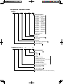
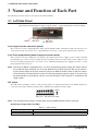
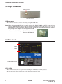
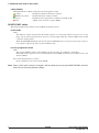
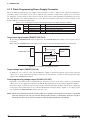
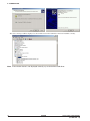
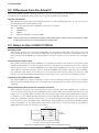
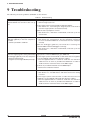
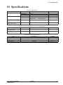
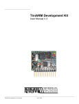
CMOS 16-BIT SINGLE CHIP MICROCOMPUTER
S5U1C17001H User Manual
(ICD Mini Ver. 1.0)
NOTICE
No part of this material may be reproduced or duplicated in any form or by any means without the written permission
of Seiko Epson. Seiko Epson reserves the right to make changes to this material without notice. Seiko Epson does not
assume any liability of any kind arising out of any inaccuracies contained in this material or due to its application or
use in any product or circuit and, further, there is no representation that this material is applicable to products requiring high level reliability, such as medical products. Moreover, no license to any intellectual property rights is granted by
implication or otherwise, and there is no representation or warranty that anything made in accordance with this material will be free from any patent or copyright infringement of a third party. This material or portions thereof may contain
technology or the subject relating to strategic products under the control of the Foreign Exchange and Foreign Trade
Law of Japan and may require an export license from the Ministry of Economy, Trade and Industry or other approval
from another government agency.
Windows 2000 and Windows XP are registered trademarks of Microsoft Corporation, U.S.A.
PC/AT and IBM are registered trademarks of International Business Machines Corporation, U.S.A.
All other product names mentioned herein are trademarks and/or registered trademarks of their respective owners.
© SEIKO EPSON CORPORATION 2007, All rights reserved.
Configuration of product number
Devices
S1
C
17xxx
F
00E1
00
Packing specifications
00 : Besides tape & reel
0A : TCP BL
2 directions
0B : Tape & reel BACK
0C : TCP BR
2 directions
0D : TCP BT
2 directions
0E : TCP BD
2 directions
0F : Tape & reel FRONT
0G : TCP BT
4 directions
0H : TCP BD
4 directions
0J : TCP SL
2 directions
0K : TCP SR
2 directions
0L : Tape & reel LEFT
0M: TCP ST
2 directions
0N : TCP SD
2 directions
0P : TCP ST
4 directions
0Q : TCP SD
4 directions
0R : Tape & reel RIGHT
99 : Specs not fixed
Specification
Package
D: die form; F: QFP, B: BGA
Model number
Model name
C: microcomputer, digital products
Product classification
S1: semiconductor
Development tools
S5U1
C
17000
H2
1
00
Packing specifications
00: standard packing
Version
1: Version 1
Tool type
Hx : ICE
Dx : Evaluation board
Ex : ROM emulation board
Mx : Emulation memory for external ROM
Tx : A socket for mounting
Cx : Compiler package
Sx : Middleware package
Corresponding model number
17xxx: for S1C17xxx
Tool classification
C: microcomputer use
Product classification
S5U1: development tool for semiconductor products
COnTenTS
- Contents 1 Overview......................................................................................................................... 1
1.1 Features ............................................................................................................................ 2
1.2 Operating Environment ..................................................................................................... 2
2 Components Included with Package ........................................................................... 3
3 name and Function of each Part ................................................................................. 4
3.1 Left Side Panel .................................................................................................................. 4
3.2 Right Side Panel................................................................................................................ 6
3.3 Top Panel........................................................................................................................... 6
4 Connections ................................................................................................................... 9
4.1 Connecting the Target System .......................................................................................... 9
4.1.1 Target Interface Connector.................................................................................. 9
4.1.2 Flash Programming Power Supply Connector ................................................... 10
4.2 Connecting to the Host Computer .................................................................................... 11
5 ICD Mode ....................................................................................................................... 13
5.1 Specifying ICD Mode ....................................................................................................... 13
5.2 Activation in ICD Mode ..................................................................................................... 13
5.2.1 When the TARGET RST OUT Signal is Not Connected .................................... 13
5.2.2 When the TARGET RST OUT Signal is Connected ........................................... 14
5.3 Starting Up the Debugger ................................................................................................ 14
5.4 Connection Test................................................................................................................ 15
6 Flash Programmer Mode ............................................................................................. 16
6.1 Preparation for Flash Programming ................................................................................. 16
6.2 Operations in Flash Programmer Mode ........................................................................... 17
7 Firmware Update .......................................................................................................... 18
8 Precautions ................................................................................................................... 19
8.1 Restrictions on Debugging ............................................................................................... 19
8.2 Differences from the Actual IC ......................................................................................... 20
8.3 Notes on Use of S5U1C17001H ...................................................................................... 20
9 Troubleshooting ............................................................................................................ 22
10 Specifications ............................................................................................................. 23
S5U1C17001H User ManualEPSON
(ICD Mini Ver. 1.0)
i
EXPlaNaTION OF TErMS
Explanation of Terms (various modes)
S5U1C17001H (ICD Mini)
ICD mode
Flash programmer mode
This mode is for debugging the target.
The debugging requires a PC and the debugger gdb
(included in the S5U1C17001C S1C17 Family C Compiler
Package).
This mode is for programming the Flash of the target
w i t h o u t a P C u s e d . B e fo r e p r o gra m m i n g c a n b e
performed, the program to be written must be loaded to
the S5U1C17001H (ICD Mini) in ICD mode.
Debugger gdb (included in the S5U1C17001C S1C17 Family C Compiler Package)
Connect mode
Simulator (SIM) mode
ICD Mini mode
The simulator mode simulates the target program
execution on the PC memory and no other tools are not
required. However, the debug functions depending on the
ICD cannot be used.
This is the mode to debug the target program using the
S5U1C17001H (ICD Mini) or ICD board. The program will
be executed on the target board. The S5U1C17001H (ICD
Mini) must be used in this mode.
Target (S1C17xxx)
Normal mode
Debug mode
The normal mode is the normal state while the target is
executing the user program.
The target enters debug mode by one of the conditions
shown below.
• When a beak condition set by the debugger gdb has
met
• When the break button on the gdb window is clicked
while the debugger is connected to the target
• When a low level signal is input to the DSIO pin of the
target
• When the CPU executes the brk instruction
In this mode, the target accepts the control by the
debugger gdb.
Various debugging operations, such as display and
rewriting the registers/memory, can be performed.
The target enters this mode when executing the startup
sequence after connecting it to the S5U1C17001H (ICD
Mini).
ii
EPSON
S5U1C17001H User Manual
(ICD Mini Ver. 1.0)
1 OVerVIeW
1 Overview
The S5U1C17001H (ICD Mini) is a hardware tool (emulator) that allows software to be efficiently developed for
the S1C17 Family of 16-bit processors. The S5U1C17001H provides a software development environment with the
debugger (gdb.exe) by communicating it to the S1C17 processor on the target system and the debugger. In addition
to debugging, it can be used as a Flash programmer to program the Flash memory built into the S1C17 processor
on the target system.
This manual primarily explains how to use the S5U1C17001H. For details on the debugger functions and
commands, refer to the “Debugger” section in the “S5U1C17001C Manual (C Compiler Package for S1C17
Family).”
S5U1C17001H External View
Note: Do not open the case as it may cause a malfunction.
Precautions before using the S5U1C17001H
Please read the sections shown below before getting started with the S5U1C17001H. These sections, especially (2)
and (3), describe the answers to frequently asked questions.
(1) Chapter 2, Components Included with Package
Make sure all of the listed items are included with your package.
(2) Section 4.2, Connecting to the Host Computer
Install the USB driver before the S5U1C17001H can be used.
(3) Section 4.1, Connecting the Target System
Please pay particular attention to the Notes.
S5U1C17001H User ManualEPSON
(ICD Mini Ver. 1.0)
1
1 OVerVIeW
1.1 Features
• S1C cores supported
S1C17 Core
S1C33 STD Core *1
S1C33 mini Core *1
S1C33 PE Core *1
S1C33 ADV Core *1
• Host interface
USB 1.1
• Data download rate
Approx. 65KB/s when DCLK = 40 MHz (Max.) *2
Approx. 50KB/s when DCLK = 20 MHz *2
• Debugger mode
ICD Mini mode
• Program break functions
PC break function
Lapse of time break function
Forced break function
External forced break function (BRK IN pin input)
• Measurement of program execution time
Can be measured from within 3 µs to 6515 hours
• Standalone Flash programmer function
Available
• Firmware update function
Available
• DCLK frequency to communicate with the target
4 kHz to 40 MHz
• Flash programming power voltage supply
Available
• Target reset signal output
Available
• Target system I/O interface voltage
3.3 V, 1.8 V, or voltage (1.0 to 5.0 V) input from the target
• Target system interface connector
4-pin connector
• Flash programming power supply connector
4-pin connector
*1 Scheduled to be supported with a firmware update
*2 The frequency assumes that the I/O voltage is 3.3 V. The maximum frequency may be lower than the spec value
due to ambient noise, temperature condition, product type, and unevenness in quality.
1.2 Operating environment
As the host computer, the S5U1C17001H uses a PC with a USB port (USB 1.1) available. Windows 2000 or Windows XP is recommended for the OS.
2EPSON
S5U1C17001H User Manual
(ICD Mini Ver. 1.0)
2 COMPOnenTS InClUDeD WITH PaCKaGe
2 Components Included with Package
The following shows the components included with the S5U1C17001H package:
(1)
(2)
(3)
(4)
(5)
(6)
(7)
(8)
S5U1C17001H (main unit) ........................................... 1
USB cable...................................................................... 1
Target interface cable (4-pin) ........................................ 1
Flash programming power supply cable (4-pin) ........... 1
User registration card .................................................... English/Japanese, 1 each
Warranty card ................................................................ English/Japanese, 1 each
Usage precautions ......................................................... English/Japanese, 1 each
Manual download guide ................................................ English/Japanese, 1 each
The items specified below are not included with the package. These items must be prepared separately.
(9)
S5U1C17001H User Manual (ICD Mini Ver. 1.0) (this PDF, downloadable from the SEIKO EPSON HP)
When developing an S1C17 application
(10) Debugger (gdb.exe) for the S1C17 Family (included in the S1C17 Family C Compiler Package)
(11) Debugger manual for the S1C17 Family (included in the S1C17 Family C Compiler Package)
When developing an S1C33 application (scheduled to be supported)
(10) Debugger (gdb.exe) for the S1C33 Family (included in the S1C33 Family C Compiler Package)
(11) Debugger manual for the S1C33 Family (included in the S1C33 Family C Compiler Package)
Figure 2.1 Components in the S5U1C17001H Package
S5U1C17001H User ManualEPSON
(ICD Mini Ver. 1.0)
3
3 naMe anD FUnCTIOn OF eaCH ParT
3 Name and Function of Each Part
The following shows the name of each part of the S5U1C17001H.
3.1 left Side Panel
4-pin Flash programming power supply connector (white)
GND pin
BRK IN pin
4-pin target interface connector (black)
DIP switch
Left Side Panel
4-pin target interface connector (black)
This connector is used to input/output the debug signals (DCLK, DSIO, and DST2) from/to the S1C processor
on the target system. See Section 4.1.1, “Target Interface Connector,” for the pin assignment and connection.
4-pin Flash programming power supply connector (white)
This connector is used to output the reset signal to the target system and to supply a power voltage for Flash
programming (Note). Also it is used to input the target operating voltage when the target system voltage level is
used for the debug signal interface. See Section 4.1.2, “Flash Programming Power Supply Connector,” for the
pin assignment and connection.
Note: The S5U1C17001H is equipped with a 7-V Flash programming power supply with output capacities of 200 mA. Note, however, that its usage depends on the S1C processor. Be sure to avoid using this power supply for the S1C processor (do not set SW8 of the DIP switch to ON) if its technical manual does not describe the usage of the Flash programming power supply, as the chip may
be destroyed due to overvoltage. This pin must be left open if the connector is attached on the
target system.
DIP switch
The DIP switch assembly is used to select the target CPU core, Flash programmer mode, DSIO signal level,
connection test feature, firmware update feature, and Flash programming voltage output.
OPEN
1
2
3
4
5
6
7
8
ON
Figure 3.1.1 DIP Switch Assembly
Note: The changed switch settings will take effect after the RESET/START switch is pressed.
Selecting the target CPU core (SW1)
Table 3.1.1 SW1 Settings
SW1
OPEN (↑)
ON (↓)
Setting
S1C17 Core (default)
S1C33 Core *
* Scheduled to be supported with a firmware update
4EPSON
S5U1C17001H User Manual
(ICD Mini Ver. 1.0)
3 naMe anD FUnCTIOn OF eaCH ParT
Selecting either ICD mode or Flash programmer mode (SW2 and SW3)
Table 3.1.2 SW2 and SW3 Settings
SW2
SW3
OPEN (↑)
ON (↓)
OPEN (↑)
ON (↓)
OPEN (↑)
OPEN (↑)
ON (↓)
ON (↓)
Setting
ICD mode (default)
Flash programmer mode
Flash programmer mode
Flash programmer mode
Erase → program
Verify
Erase → program → verify
In ICD mode, the debugger on the PC controls the S5U1C17001H to execute the debug commands. (See Chapter 5.)
In Flash programmer mode, the S5U1C17001H operates as a standalone Flash programmer. (See Chapter 6.)
Selecting the DSIO signal level (SW4 and SW5)
Table 3.1.3 SW4 and SW5 Settings
SW4
SW5
OPEN (↑)
OPEN (↑)
ON (↓)
OPEN (↑)
ON (↓)
–
Setting
3.3 V (default)
1.8 V
Voltage (1.0 to 5.0 V) input from the target
The target operating voltage should be input to Pin 4 on the Flash programming power supply connector.
enabling the connection test (SW6)
Table 3.1.4 SW6 Settings
SW6
OPEN (↑)
ON (↓)
Setting
Omitt connection test (default)
Execute connection test
The connection test is a communication diagnostic feature at start up of the debugger.
Setting firmware update mode (SW7)
Table 3.1.5 SW7 Settings
SW7
OPEN (↑)
ON (↓)
Setting
OFF (default)
ON
When SW7 is set to ON, a connection between the S5U1C17001H and the debugger can be established even if a
target is not connected. See Chapter 7, “Firmware Update,” for how to update the firmware.
enabling voltage output for Flash programming (SW8)
Table 3.1.6 SW8 Settings
SW8
OPEN (↑)
ON (↓)
Setting
OFF (default)
ON
Note: The S5U1C17001H is equipped with a 7-V Flash programming power supply with output capacities of 200 mA. Note, however, that its usage depends on the S1C processor. Be sure to avoid using this power supply for the S1C processor (do not set SW8 of the DIP switch to ON) if its technical manual does not describe the usage of the Flash programming power supply, as the chip may
be destroyed due to overvoltage.
BrK In pin
In ICD mode, if a low-level signal is input to this pin when the target program is being executed, the target
program execution is suspended. After a low level is input to the BRK IN pin, a break will occur after a few instructions have been executed.
In Flash programmer mode, inputting a low level to this pin has the same function as pressing the RESET/
START switch (it starts erasing/programming/verification).
Note: The voltage to apply to the BRK IN pin must be 0 V for low level and 3.3 V or open for high level.
The BRK IN pin is always pulled up to 3.3 V.
GnD pin
Connect this pin to the GND level (0 V).
S5U1C17001H User ManualEPSON
(ICD Mini Ver. 1.0)
5
3 naMe anD FUnCTIOn OF eaCH ParT
3.2 right Side Panel
USB connector
Right Side Panel
USB connector
This connector is used to connect to a PC using the supplied USB cable.
Note: When a bus-powered USB hub is used to connect the S5U1C17001H to the PC, there may be a
shortage of drive power. Connect the S5U1C1700H directly to a PC’s USB port, or use a 5-V AC
adapter with a USB connector for supplying power* especially when supplying the Flash programming voltage to the target in Flash programmer mode.
* Recommended AC adapters:ELECOM AVD-ACAU1WH
Groovy GM-PW001A
3.3 Top Panel
LED1
LED2
LED3
LED4
RESET/START switch
Top Panel
leD1–leD4
The four LEDs located on the top panel indicate debugging and Flash programming statuses.
The indicated status differs between ICD mode and Flash programmer mode.
6EPSON
S5U1C17001H User Manual
(ICD Mini Ver. 1.0)
3 naMe anD FUnCTIOn OF eaCH ParT
In ICD mode
leD1 (CPU)
This LED indicates the target CPU selected using SW1.
l (blue) C17: Target CPU is an S1C17xxx or a product in which the S1C17 Core is embedded.
l (green) C33: Target CPU is an S1C33xxx or a product in which the S1C33 Core is embedded.
* C33 is scheduled to be supported with a firmware update.
leD2 (ICD MODe)
This LED always lights in blue (l) when ICD mode is selected using SW2 and SW3.
l (blue) The S5U1C17001H is being operated in ICD mode.
leD3 (eMU)
This LED lights when the target program is started from the debugger to indicate that the target system is
executing the target program. Also this LED lights when the target system is in power-off status or it is not
connected. In this case, the LED will go out by turning the target system on or by pressing the RESET/
START switch after connecting the target system properly.
l (red)
• The target system is in power-off status.
• The target system is not connected properly.
• The target system is executing the user program.
l (out)
Other
leD4 (DBG)
This LED indicates that the target S1C processor is placed in debug mode.
l (green) The target S1C processor is placed in debug mode.
Also this LED rights with LED3 before the initial connection between the S5U1C17001H and
the target S1C processor has been established.
l (out)
Other
In Flash programmer mode
When the S5U1C17001H starts up in Flash programmer mode, LED2 lights in white ( ), LED3 lights in
magenta (l), or LED4 lights in yellow (l).
leD1 (CPU)
This LED indicates the target CPU selected using SW1.
l (blue) C17: Target CPU is an S1C17xxx or a product in which the S1C17 Core is embedded.
l (green) C33: Target CPU is an S1C33xxx or a product in which the S1C33 Core is embedded.
* C33 is scheduled to be supported with a firmware update.
leD2 (eraSe)
This LED indicates a Flash erasing selection/operation status.
(white)
The Flash erasing function is selected.
(blinking in white)
The Flash memory is being erased.
l (green)
The Flash erasing operation has completed normally. (OK)
l (red)
A Flash erase error has occurred. (ERR)
leD3 (WrITe)
This LED indicates a Flash programming selection/operation status.
l (magenta)
The Flash programming function is selected.
W (blinking in magenta) The Flash memory is being programmed.
l (green)
The Flash programming operation has completed normally. (OK)
l (red)
A Flash program error has occurred. (ERR)
S5U1C17001H User ManualEPSON
(ICD Mini Ver. 1.0)
7
3 naMe anD FUnCTIOn OF eaCH ParT
leD4 (VerIFY)
This LED indicates a Flash verification selection/operation status.
l (yellow)
The Flash verification function is selected.
W (blinking in yellow)
The Flash memory is being verified.
l (green)
The Flash verify operation has completed normally. (OK)
l (red)
A Flash verify error has occurred. (ERR)
reSeT/STarT switch
The function differs between ICD mode and Flash programmer mode.
In ICD mode
Click:
The firmware restarts and performs the initial sequence for connecting with the S1C processor on the
target system. If the target board has not been connected physically, the S5U1C17001H enters initial
connection waiting status.
When the TARGET RST OUT signal of the S5U1C17001H has been connected to the target system, a
reset signal is output to the target system simultaneously.
In Flash programmer mode
Click:
The S5U1C17001H starts the selected Flash operation (erasing, programming, verification).
If the LED for the operation to be executed indicates OK or ERR, a hardware reset will be issued to the
S5U1C17001H.
Press and hold (about three seconds):
Issues a hardware reset to the S5U1C17001H.
Note: When a DIP switch setting is changed, it will take effect by pressing the RESET/START switch (in
both ICD and Flash programmer modes).
8EPSON
S5U1C17001H User Manual
(ICD Mini Ver. 1.0)
4 COnneCTIOnS
4 Connections
4.1 Connecting the Target System
4.1.1 Target Interface Connector
The 4-pin target interface connector (black) on the S5U1C17001H is used to input/output the debug signals from/
to the S1C processor on the target system. Use the target interface cable attached to the S5U1C17001H to connect
between this connector and the target system. This connection is always required to perform debugging. The pin
assignment of the 4-pin connector (black) on the S5U1C17001H is shown in the table below. For the debug pin
numbers on the S1C processor, refer to the technical manual of each model.
Table 4.1.1.1 Pin Assignment of the Target Interface Connector (Black)
no.
4 3 21
••••
1
2
3
4
Pin name
DCLK
GND
DSIO
DST2
I/O
I
–
I/O
I
Pin function
Clock signal input pin for debugging
Power supply GND pin
Serial transfer I/O pin for debugging
Debug status signal input pin
S5U1C17001H
Target system
S1C processor Within 5 cm
DST2
DSIO
GND
DCLK
Target interface cable
4
3
2
1
4
3
2
1
4
3
2
1
Blue
4
3
2
1
White
Place a 33 Ω resistor in series at a location
as close to the S1C processor as possible.
Target interface connector
Figure 4.1.1.1 Connecting the Target System
Notes: • Set the interface level (3.3 V/1.8 V/target input) using the DIP switches SW4 and SW5, and
select the CPU Core using the SW1 according to the target system before connecting the target system.
• The signals connected to the S5U1C17001H are very high-speed signals, so the connector
on the target system must be mounted within 5 cm from the S1C processor. If there is more
distance between the connector and the S1C processor, the S5U1C17001H may not work
properly.
• When wiring the S1C processor to the target connector for connecting the S5U1C17001H, insert a 33 W resistor in series between the S1C processor DSIO pin and the connector. This resistor must be placed as close to the S1C processor as possible. Although the system can operate without this 33 W resistor, we recommend inserting this resistor to prevent malfunctions.
The other pins are connected directly. A low-level input to the DSIO pin issues a forced break
to set the S1C processor into debug mode. Although this signal is pulled up through about 100
kW internally, when not debugging, we recommend either removing the 33 W resistor to reduce
noise and other problems or pulling this line up to the VDD level (the core voltage).
• Be sure to use the supplied 4-pin cable for connecting the target system to the S5U1C17001H.
Using another cable may cause a malfunction. If another cable must be necessarily used, do
not extend the target interface cable and connect the cable directly to the S5U1C17001H so
that the distance to the S1C processor on the target system will be shortest.
• The 4-pin connector does not have a projection for preventing reverse insertion. Check the
cable color (blue) of pin 1 to be sure the insertion of connector is proper when connecting it to
the target system.
S5U1C17001H User ManualEPSON
(ICD Mini Ver. 1.0)
9
4 COnneCTIOnS
4.1.2 Flash Programming Power Supply Connector
The 4-pin Flash programming power supply connector (white) is used to output a reset signal and a Flash programming voltage to the target system, and to input the target interface voltage. These signals are not necessary
for debugging. Connect between this connector and the target system using the Flash programming power supply cable attached to the S5U1C17001H as necessary. The pin assignment of the 4-pin connector (white) on the
S5U1C17001H is shown in the table below.
Table 4.1.2.1 Pin Assignment of the Flash Programming Power Supply Connector (White)
1 2 34
••••
no.
Pin name
I/O
1
2
3
4
FLASH VCC OUT
GND
TARGET RST OUT
TARGET VCC IN
O
–
O
I
Pin function
Flash programming voltage output pin
Power supply GND pin
Target reset signal output pin
Target voltage input pin
* Pay attention to the pin number assignment. (It is the reverse order of the target interface connector.)
Target reset signal output (TarGeT rST OUT)
By pressing the RESET/START switch in ICD mode, the TARGET RST OUT outputs a reset signal to the target system.
When using the TARGET RST OUT output, a reset circuit as shown in the figure below is recommended.
S5U1C17001H
TARGET RST OUT
Target system
4
3
2
1
Pull-up resistor
S1C processor
#RESET
Reset circuit on
the target system
Reset switch
Figure 4.1.2.1 Example of Target Reset Circuit
Target voltage input (TarGeT VCC In)
In addition to 3.3 V and 1.8 V, the S5U1C17001H is capable of interfacing with the target system using the
voltage (1.0 to 5.0 V) input from the target system. To use this function, set SW4 to ON and input the target
voltage to the TARGET VCC IN pin.
Flash programming voltage output (FlaSH VCC OUT)
Depending on the Flash memory module built into the S1C processor on the target system, its programming
voltage (7 V) can be supplied from the S5U1C17001H. The maximum current that can be supplied is 200 mA.
To use this output, set SW8 to ON and connect between the FLASH VCC OUT pin and the power supply pin
on the target system. When SW8 is set to ON, the FLASH VCC OUT pin always outputs a 7-V voltage regardless of whether the RESET/START switch is pressed or not.
Note: Refer to the technical manual of each model as to whether the target S1C processor is operable
with this voltage or not. Do not use this voltage unless there is a description about the usage in
the technical manual, as the S1C processor may be destroyed due to overvoltage.
10EPSON
S5U1C17001H User Manual
(ICD Mini Ver. 1.0)
4 COnneCTIOnS
4.2 Connecting to the Host Computer
Use the attached USB cable to connect the S5U1C17001H to the host computer. When the S5U1C17001H is connected to the host computer for the first time, the host computer will request that the USB driver be installed. Install
the USB driver by the procedure shown below. The USB driver is located in the “C:\EPSON\gnu17\utility\drv_usb”
directory created when the S5U1C17001C (S1C17 Family C Compiler Package) was installed.
USB driver installation procedure
(1) First time the S5U1C17001H is connected to the host computer with the USB cable, the dialog box shown
below will be displayed.
(2) Install the USB driver by following the directions displayed by the wizard.
Specify “C:\EPSON\gnu17\utility\drv_usb” as the USB driver directory.
S5U1C17001H User ManualEPSON
(ICD Mini Ver. 1.0)
11
4 COnneCTIOnS
The device manager will be displayed as shown below when the USB driver has been installed correctly.
Note: If the window above is not displayed correctly, try to reinstall the USB driver.
12EPSON
S5U1C17001H User Manual
(ICD Mini Ver. 1.0)
5 ICD MODe
5 ICD Mode
ICD mode is an S5U1C17001H operating mode for debugging the target system by connecting the S5U1C17001H
to the debugger (gdb.exe) on the PC. The following explains the settings for activating ICD mode and operations.
5.1 Specifying ICD Mode
Set the DIP switches as below so that the S5U1C17001H will start up in ICD mode.
SW2 = OPEN
SW3 = OPEN
5.2 activation in ICD Mode
After connecting the S5U1C17001H to the target system and the host computer, start up the S5U1C17001H by following the procedure described below. If the S5U1C17001H is started up in another procedure, it may not be connected to the target system normally.
5.2.1 When the TarGeT rST OUT Signal is not Connected
When the TARGET RST OUT signal is not connected to the reset input on the target system, start up the
S5U1C17001H by the procedure described below.
(1) Hold down the RESET/START switch on the S5U1C17001H.
LED1
(white)
LED2
(white)
LED3
(white)
LED4 l (out)
(2) Hold down the reset switch on the target system.
(3) Release the RESET/START switch on the S5U1C17001H.
LED1 l (blue)
LED2 l (blue)
LED3 l (red)
LED4 l (green)
(4) Release the reset switch on the target system.
When the S5U1C17001H has been connected to the target S1C processor normally
LED1 l (blue)
LED2 l (blue)
LED3 l (out)
LED4 l (green)
When the S5U1C17001H has not been connected to the target system
LED1 l (blue)
LED2 l (blue)
LED3 l (red)
LED4 l (out)
In this case, retry from Step (1).
S5U1C17001H User ManualEPSON
(ICD Mini Ver. 1.0)
13
5 ICD MODe
5.2.2 When the TarGeT rST OUT Signal is Connected
When the TARGET RST OUT signal is connected to the reset input on the target system, just press the RESET/
START switch on the S5U1C17001H for starting up. The S5U1C17001H automatically generates a target reset signal with the proper connection sequence.
(1) Press the RESET/START switch on the S5U1C17001H.
LED1
(white)
LED2
(white)
LED3
(white)
LED4 l (out)
(2) Release the RESET/START switch on the S5U1C17001H.
When the S5U1C17001H has been connected to the target S1C processor normally
LED1 l (blue)
LED2 l (blue)
LED3 l (out)
LED4 l (green)
When the S5U1C17001H has not been connected to the target system
LED1 l (blue)
LED2 l (blue)
LED3 l (red)
LED4 l (out)
In this case, retry from Step (1).
5.3 Starting Up the Debugger
Start up the debugger (gdb.exe) on the PC after the connection between the S5U1C17001H and the target S1C processor has been established by the operations described above.
When debugging using the debugger with the S5U1C17001H connected, the debugger must be set to ICD Mini
mode by executing the target command.
(gdb) target icd usb ← Command to set the debugger in ICD Mini mode
For the debug commands and how to operate the debugger, refer to the “S5U1C17001C Manual (C Compiler Package for S1C17 Family).”
Note: Before disconnecting the S5U1C17001H from the host computer, be sure to terminate the debugger.
14EPSON
S5U1C17001H User Manual
(ICD Mini Ver. 1.0)
5 ICD MODe
5.4 Connection Test
The S5U1C17001H has a connection test feature to diagnose if it can communicate with the target system properly
when the debugger (gdb.exe) starts up. Perform the connection test, for example, when the S5U1C17001H does not
start up by the correct procedure. Use the DIP switch to select whether the connection test will be omitted or executed.
Omitting the connection test (default)
When SW6 is set to OPEN, the S5U1C17001H will omit the connection test at the start up of the debugger (gdb.
exe).
executing the connection test
When SW6 is set to ON, the S5U1C17001H will execute the connection test at the start up of the debugger (gdb.
exe).
S5U1C17001H User ManualEPSON
(ICD Mini Ver. 1.0)
15
6 FlaSH PrOGraMMer MODe
6 Flash Programmer Mode
Flash programmer mode is an S5U1C17001H operating mode for using it as a standalone Flash programmer. The
following explains the settings for activating the Flash programmer mode and operations.
6.1 Preparation for Flash Programming
The Flash programming feature allows programming the target system’s Flash memory with data such as a program, which has been downloaded into the S5U1C17001H’s internal Flash memory.
First download the data to program the target system’s Flash memory into the S5U1C17001H by the procedure described below.
(1) Convert the file for programming the Flash memory into a Motorola S3 file.
Use “objcopy.exe” included in the S1C17 Family C Compiler Package for file conversion.
Example: 1. Convert “sample.elf” into a Motorola S3 file.
>objcopy -O srec -R .gbss --srec-forceS3 sample.elf sample.sa
2. Fill the unused addresses in “sample.sa” and generate “sample.saf.”
(when the start address and block size to be filled are 0x8000 and 0x1000, respectively)
>moto2ff 0x8000 1000 sample.sa
(2) Start up the S5U1C17001H in ICD mode (see Section 5.2).
(3) Start up the debugger.
1. Launch GDB.
>gdb
2. Connect the target.
(gdb) target icd usb
(4) If the S5U1C17001H contains an unnecessary program/data used previously, clear it using the c17 fwe command.
(5) Download a Flash erase/program routine into the S5U1C17001H using the c17 fwlp command.
Example: Load the data erase/write program file “writer.sa.”
(when the erase routine start address is 0x4c and the write routine start address is 0x80)
(gdb) c17 fwlp writer.sa 0x4c 0x80
(6) Download the data for programming the target system’s Flash memory into the S5U1C17001H using the c17
fwld (or c17 fwdc) command. At the same time, specify the range of the Flash memory to be erased.
Example: Erase all sectors and load “sample.saf” to the Flash.
(when the Flash start address is 0x8000)
(gdb) c17 fwld sample.saf 0 0 0x8000
(7) Quit the debugger.
For details of the debugger (gdb.exe) and “objcopy.exe,” refer to the “S5U1C17001C Manual (C Compiler Package
for S1C17 Family).”
16EPSON
S5U1C17001H User Manual
(ICD Mini Ver. 1.0)
6 FlaSH PrOGraMMer MODe
6.2 Operations in Flash Programmer Mode
The following describes how to start up the S5U1C17001H and procedure for Flash programming.
(1) Set SW2 and SW3 according to the Flash operation to be performed.
One of the three sequences, erasing and programming, verification only, or erasing, programming, and verification, can be selected.
Table 6.2.1 DIP Switch Settings in Flash Programmer Mode
SW2
SW3
OPEN (↑)
ON (↓)
OPEN (↑)
ON (↓)
OPEN (↑)
OPEN (↑)
ON (↓)
ON (↓)
Setting
ICD mode (default)
Flash programmer mode
Flash programmer mode
Flash programmer mode
Erase → program
Verify
Erase → program → verify
(2) If the DIP switch is changed when power is supplied through the USB cable, press the RESET/START switch
to set the S5U1C17001H to Flash programmer mode.
If the DIP switch is changed during power off, supply power by connecting the S5U1C17001H USB cable to a
USB port on the host computer or an AC adapter with a 5-V USB output (see Section 3.2). (Flash programmer
mode needs only a power supplied through the USB cable and it does not communicate with the PC.) When the
S5U1C17001H starts up in Flash programmer mode normally, the LCDs light according to the selected operation.
l ERASE
l WRITE
l VERIFY
Erase → program
(white)
l (magenta)
l (out)
Verify
l (out)
l (out)
l (yellow)
Erase → program → verify
(white)
l (magenta)
l (yellow)
(3) Connect the target system including the Flash to be programmed to the S5U1C17001H.
(4) Press the RESET/START switch.
The S5U1C17001H starts the selected Flash operation.
The LED indicates the operation being executed.
l ERASE
l WRITE
l VERIFY
During erasing
(blinking in white)
–
–
During programming
–
W (blinking in magenta)
–
During verification
–
–
W (blinking in yellow)
(5) When the Flash operation has finished, the LED lights as shown below to indicate that the operation has completed normally or an error has occurred.
When completed normally
l ERASE
l WRITE
l VERIFY
Erasing has completed
l (green)
–
–
Programming has completed
–
l (green)
–
Verification has completed
–
–
l (green)
Program error
–
l (red)
–
Verify error
–
–
l (red)
When an error has occurred
l ERASE
l WRITE
l VERIFY
Erase error
l (red)
–
–
(6) Disconnect the target system.
(7) Return to Step (3) to continue the same Flash operation.
Return to Step (1) to change the Flash operation.
When finishing Flash programming, disconnect the USB cable and set the DIP switch back to ICD mode.
S5U1C17001H User ManualEPSON
(ICD Mini Ver. 1.0)
17
7 FIrMWare UPDaTe
7 Firmware Update
The S5U1C17001H has a firmware update function using the debugger (gdb.exe). The following shows the procedure to update the S5U1C17001H firmware.
Note: Before the firmware can be updated, the USB driver must be installed.
(1) Connect the S5U1C17001H with the host computer using the USB cable.
(2) Set the DIP switch on the S5U1C17001H as below, then press the RESET/START switch.
SW2 = OPEN
SW3 = OPEN
SW7 = ON
(3) Start up the debugger (gdb.exe).
To invoke at the command prompt:
>C:
>cd \EPSON\gnu17
>gdb
(4) Enter the commands shown below after the debugger starts up.
(gdb) target icd usb
(gdb) c17 firmupdate path\filename.sa
(5) The firmware update has completed when the LEDs light as below.
LED1 l (blue)
LED2 l (green)
LED3 l (green)
LED4 l (green)
(6) Set SW7 to OPEN and press the RESET/START switch to restart the S5U1C17001H.
If a malfunction occurs during a firmware update and the S5U1C17001H does not operate normally, please contact
our sales office.
18EPSON
S5U1C17001H User Manual
(ICD Mini Ver. 1.0)
8 PreCaUTIOnS
8 Precautions
8.1 restrictions on Debugging
The debugging using the S5U1C17001H is subject to the restrictions specified below.
Operation of the internal peripheral circuits
The peripheral circuits of the target S1C processor stop operating when the debugger (gdb.exe) on the host
computer is ready to accept commands, that is, unless the target program is running. For this reason, the peripheral circuits do not operate in real time when the target program is executed in the single-step mode. For details
on single-step execution, refer to the “Debugger” section in the “S5U1C17001C Manual (C Compiler Package
for S1C17 Family)”.
Interrupts when the target program is not running
If an interrupt request to the S1C Core is generated by the target system when the target program is not running,
interrupt processing is paused. The interrupt that has been paused is serviced immediately before the target
program is executed or immediately after one instruction is executed after the debugger (gdb.exe) on the host
computer has directed that the target program be executed.
Interrupts when the target program is executed in a single step
If an interrupt request to the S1C Core is generated by the target system during single-step execution of the
target program, including functions and subroutines (STEP), the interrupt request is paused. During single-step
execution of the target program, not including functions and subroutines (NEXT), an interrupt request received
within a function or subroutine is serviced without being paused and an interrupt received in other parts of the
program is paused as with the STEP command. The interrupt that has been paused is serviced immediately before the target program is executed or immediately after one instruction is executed after the debugger (gdb.exe)
on the host computer has directed that the target program be executed. For details on single-step execution (STEP
and NEXT), refer to the “Debugger” section in the “S5U1C17001C Manual (C Compiler Package for S1C17
Family)”.
execution counter
The execution counter is capable of measuring execution times up to 6515 hours with a ±1 µs of measurement
error. A 3 µs or less of program execution time cannot be measured correctly.
The counter is also used for clocking of the lapse of time break function, therefore, execution times cannot be
measured when the lapse of time break function is used.
reset sequence
The sequence from when the S5U1C17001H is powered on until the target program is executed is entirely different from that of the actual S1C processor.
However, a sequence for the reset request input from the target system while the target program is being executed is the same as that for the actual S1C processor.
Regarding the reset sequence in the actual S1C processor, refer to the technical manual of each model.
Break functions when a reset request is accepted
If a reset request (reset input or reset interrupt from the watchdog timer) is accepted while the S1C processor
on the target system is executing the target program in normal mode, the hardware PC break and software PC
break functions are disabled. It will be enabled again when the S1C processor enters debug mode.
I/O memory dump by the S5U1C17001H
Note that some S1C peripheral circuits may change the control register status due to their specifications when
the I/O memory is read using the memory dump function of the S5U1C17001H or when the target program execution is suspended.
For details on the memory dump function, refer to the “Debugger” section in the “S5U1C17001C Manual (C
Compiler Package for S1C17 Family)”.
S5U1C17001H User ManualEPSON
(ICD Mini Ver. 1.0)
19
8 PreCaUTIOnS
8.2 Differences from the actual IC
The S5U1C17001H is different from the actual IC in the way specified below. If this difference is not taken into
consideration in an application, the program may not operate normally in the actual IC.
register initialization
The initial CPU register values may be different from those of the actual IC. Therefore, be sure not to create a
program that depends on the initialized value.
The initial values when the S5U1C17001H is connected are as follows:
r0–r7: 0x000000
pc:
0x008000 (Note)
sp:
0xfffffc
psr:
0x00 (IL = 000, IE = 0, CVZN = 0000)
Note: The PC initial value is decided according to the TTBR register setting value (boot address). Refer
to the technical manual of each model for the TTBR value.
8.3 notes on Use of S5U1C17001H
Powering on/off
After turning off the power to the S5U1C17001H by disconnecting the USB cable, wait at least 10 seconds
before turning the power on (connecting the USB cable) again. If the power is turned on immediately after it is
turned off, the S5U1C17001H may not be initialized correctly in a power-on reset, and may cause a malfunction.
Connecting the target system
The signals connected to the S5U1C17001H are very high-speed signals, so the connector on the target system
must be mounted within 5 cm from the target S1C processor. If there is more distance between the connector
and the S1C processor, the S5U1C17001H may not work properly. Furthermore, be sure to use the supplied
4-pin cable for connecting the target system to the S5U1C17001H. Using another cable may cause a malfunction. If another cable must be necessarily used, do not extend the target interface cable and connect the cable
directly to the S5U1C17001H so that the distance to the S1C processor on the target system will be shortest.
Operation of the S5U1C17001H system
The S5U1C17001H can work by connecting a target system in which the actual S1C processor is mounted.
Since the S5U1C17001H package does not include any board equivalent to a target system, please prepare
separately.
Wiring between the S1C processor and target connector
When wiring the S1C processor to the target connector for connecting the S5U1C17001H, insert a 33 W resistor in series between the S1C processor DSIO pin and the connector. This resistor must be placed as close to the
S1C processor as possible. If the reset line is not connected, the system can be operated without this 33 W resistor. However, we recommend inserting this resistor to prevent malfunctions. The other pins are connected directly. The total length of the line must be under 5 cm. A low-level input to the DSIO pin issues a forced break
to set the S1C processor into debug mode. Although this signal is pulled up through about 100 kW internally,
when not debugging, we recommend either removing the 33 W resistor to reduce noise and other problems or
pulling this line up to the VDD level (the core voltage).
Within 5 cm
DCLK
S1C processor
GND
DSIO
Target
connector
DST2
Place a 33 Ω resistor in series at a location
as close to the S1C processor as possible.
Figure 8.3.1 Wiring between S1C Processor and Target Connector
20EPSON
S5U1C17001H User Manual
(ICD Mini Ver. 1.0)
8 PreCaUTIOnS
reset request
Do not reset the target system while the target program execution is suspended as the S5U1C17001H will be
unable to operate normally.
notes on target system power supply
The allowable voltage range for the signals input from the target system is 0 to 5.5 V. The S5U1C17001H may
fail if voltages that exceed this range are input. Therefore, target systems to be connected to the S5U1C17001H
must be designed so that voltages outside this range are not applied. Take special care in designing the target
system power supply, and design the target system so that overvoltages are not applied to the S5U1C17001H
when the target system power supply is turned on or off.
S5U1C17001H User ManualEPSON
(ICD Mini Ver. 1.0)
21
9 TrOUBleSHOOTInG
9 Troubleshooting
The following shows the problems attributable to the hardware:
Table 9.1 Troubleshooting
Symptom
Cause/remedy
T h e L E D3 ( E M U ) t h a t l i t w h e n t h e (1)Is the target system turned on?
S5U1C17001H was turned on does not go → Turn the target system on.
out.
(2)Is the target system connected with the S5U1C17001H?
→ See Section 4.1, “Connecting the Target System,” and check to
see if the target system is connected correctly.
(3)Was the start up sequence correct?
→ See Section 5.2, “Activation in ICD Mode,” and start up in the
correct order.
The following message appears when the (1)Is the S5U1C17001H connected to the host computer correctly?
debugger (gdb.exe) in the host computer is → See Section 4.2, “Connecting to the Host Computer” and check
invoked:
to see if the S5U1C17001H is connected to the host computer
Cannot open ICD17 usb driver.
correctly.
(2)Was the debugger (gdb.exe) restar ted after resetting the
S5U1C17001H while the debugger is running?
→ See Section 5.2, “Activation in ICD Mode,” and start up in the
correct order.
The following message suddenly appears This problem is caused by low-level noise on the DSIO signal of the
while the target program is being executed by target system or when the BRK IN pin goes GND level.
the debugger (gdb.exe) in the host computer: (1)Is the target system connected with a cable other than the supplied,
Break by external break.
or is the supplied cable used with extension cables?
Program received signal SIGINT, Interrupt.
→ Use the supplied cable. If it cannot be used then use extension
cables that are as short as possible and shield them in order to
avoid occurrence of low-level noise on the DSIO signal.
(2)Is there any conductive material near the BRK IN pin?
→ Remove the conductive material.
The operation is unstable.
(1)Is the DSIO output level (SW4, SW5) set correctly?
→ See Section 3.1, “Left Side Panel,” and make sure that the setting
is correct.
(2)Is the target system connected with a cable other than the one
supplied, or is the supplied cable used with extension cables?
→ Use the supplied cable. If it cannot be used then use extension
cables that are as short as possible and shield them in order to
avoid occurrence of low-level noise on the DSIO signal.
22EPSON
S5U1C17001H User Manual
(ICD Mini Ver. 1.0)
10 SPeCIFICaTIOnS
10 Specifications
Table 10.1 Specifications
Components
S5U1C17001H
USB cable
Items
Dimensions
Input voltage
Power consumption
Length
Connector
Target system interface cable Length
(4 pins)
Flash programming power
Length
supply cable (4 pins)
Specifications
100 mm (W) × 85 mm (L) × 25 mm (H)
DC 5 V
2.5 W max.
1m
S5U1C17001H side:Standard-B type
Host PC side:
Standard-A type
Approx. 15 cm
remarks
Rubber feet included
Approx. 15 cm
Table 10.2 Recommended Connectors on the Target System
Components
Target system interface
connector (4 pins)
Flash programming power
supply connector (4 pins)
Items
Specifications
Connector
4-pin (straight): A2-4PA-2.54DS(71) (HRS)
Connector
4-pin (L angle): S04B-PASK-2 (JST)
remarks
Table 10.3 Operating Environment
Items
Operating temperature
Storage temperature
Operating humidity
Storage humidity
Specifications
5 to 35°C
-10 to 60°C
35 to 80%
20 to 90%
S5U1C17001H User ManualEPSON
(ICD Mini Ver. 1.0)
remarks
No condensation
23
International Sales Operations
AMERICA
ASIA
EPSON ELECTRONICS AMERICA, INC.
EPSON (CHINA) CO., LTD.
23F, Beijing Silver Tower 2# North RD DongSanHuan
ChaoYang District, Beijing, CHINA
Phone: +86-10-6410-6655
Fax: +86-10-6410-7320
HEADQUARTERS
2580 Orchard Parkway
San Jose, CA 95131, U.S.A.
Phone: +1-800-228-3964
Fax: +1-408-922-0238
SALES OFFICE
Northeast
301 Edgewater Place, Suite 210
Wakefield, MA 01880, U.S.A.
Phone: +1-800-922-7667
Fax: +1-781-246-5443
EUROPE
EPSON EUROPE ELECTRONICS GmbH
HEADQUARTERS
Riesstrasse 15
80992 Munich, GERMANY
Phone: +49-89-14005-0
Fax: +49-89-14005-110
SHANGHAI BRANCH
7F, High-Tech Bldg., 900, Yishan Road
Shanghai 200233, CHINA
Phone: +86-21-5423-5522
Fax: +86-21-5423-5512
EPSON HONG KONG LTD.
20/F, Harbour Centre, 25 Harbour Road
Wanchai, Hong Kong
Phone: +852-2585-4600
Fax: +852-2827-4346
Telex: 65542 EPSCO HX
EPSON Electronic Technology Development
(Shenzhen) LTD.
12/F, Dawning Mansion, Keji South 12th Road
Hi- Tech Park, Shenzhen
Phone: +86-755-2699-3828
Fax: +86-755-2699-3838
EPSON TAIWAN TECHNOLOGY & TRADING LTD.
14F, No. 7, Song Ren Road
Taipei 110
Phone: +886-2-8786-6688
Fax: +886-2-8786-6660
EPSON SINGAPORE PTE., LTD.
1 HarbourFront Place
#03-02 HarbourFront Tower One, Singapore 098633
Phone: +65-6586-5500
Fax: +65-6271-3182
SEIKO EPSON CORPORATION
KOREA OFFICE
50F, KLI 63 Bldg., 60 Yoido-dong
Youngdeungpo-Ku, Seoul, 150-763, KOREA
Phone: +82-2-784-6027
Fax: +82-2-767-3677
GUMI OFFICE
2F, Grand B/D, 457-4 Songjeong-dong
Gumi-City, KOREA
Phone: +82-54-454-6027
Fax: +82-54-454-6093
SEIKO EPSON CORPORATION
SEMICONDUCTOR OPERATIONS DIVISION
IC Sales Dept.
IC International Sales Group
421-8, Hino, Hino-shi, Tokyo 191-8501, JAPAN
Phone: +81-42-587-5814
Fax: +81-42-587-5117
S5U1C17001H User Manual
(ICD Mini Ver. 1.0)
SEMICONDUCTOR OPERATIONS DIVISION
EPSON Electronic Devices Website
http://www.epson.jp/device/semicon_e
Document code: 411153600
Issue November, 2007
Printed in Japan
L
A
Mouser Electronics
Authorized Distributor
Click to View Pricing, Inventory, Delivery & Lifecycle Information:
Epson:
S5U1C17001H1100