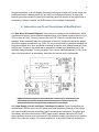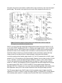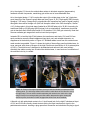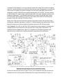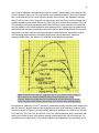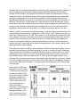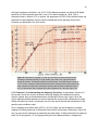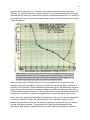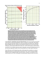
1
Rebuilt and Modified Altec 1567A:
A Technical Report
By
Clark Huckaby
http://www.clarkhuckaby.com
November, 2012
Revision July, 2013
©2012-2013 Clark Huckaby. All rights reserved.
2
Table of Contents
1. Introduction
2. The Original Altec 1567A
2.1. General Description of Original Design
2.2. Pre-Modification Condition of This Project’s Particular Altec 1567A
3. Overview of Modified Unit
3.1. General Architecture
3.2. Channels 1 Through 4
3.3. Special High-Z Circuitry in Channels 1 and 2
3.4. Channel 5
3.5. A Word About Solid-State Outputs
3.6. Clip Alert LEDs for CH1 Through CH4
3.7. Input/Output Polarity
3.8. Mechanical Layout and Power Supply
4. Schematics and Circuit Descriptions of Modified Unit
4.1. Note About Schematic Diagrams
4.2. Power Supply: Line AC and Power Transformer Primaries
4.3. Power Supply: Vintage Unit
4.4. Grounding Rule for the Modified Vintage Unit
4.5. Power Supply: Auxiliary Panel
4.6. Channels 1-4: Balanced Input Circuits
4.7. Channels 1-4: Triode Stage
4.8. Channels 1-4: Balanced Line Drivers
4.9. Channels 1-4: Clip-Alert Indicator Circuit
4.10. Channel 5
5. Performance and Applications of Modified Unit
5.1. Standard Amplitude Units
5.2. Channels 1-4: Impedance of Balanced Inputs
5.3. Channels 1-4: Modeling Balanced Pads
5.4. Channels 1, 2, and 5: Impedance and Compatibility of Unbalanced Inputs
5.5. Channels 1-4: Gain
5.6. Channels 1-4: Cross-Talk
5.7. Channels 1-4: Frequency Response
5.8. Channels1-4: Unbalanced Output Impedance and Applications
5.9. Channels 1-4: Balanced Output Characteristics
5.10. Channels 1-4: Understanding and Adjusting Clip Alerts
5.11. Channels 1-4: Types of Distortion
5.12. Channels 1 and 2: Input Transformer Saturation Threshold
5.13. Channels 1, 2 and 5: Pre-Triode Attenuator/High-Z Pad Applications and
Effect on Bandwidth
5.14. Channels 1-4: Noise
5.15. Channel 5: Applications and Input Characteristics
5.16. Channel 5: Keeping Track of Knobs
5.17. Channel 5: Variable Feedback Feature
5.18. Channel 5: Gain and Bandwidth
5.19. Channel 5: Noise and Distortion
5.20. Channel 5: Output Impedances and Transformer Characteristics
5.21. Channel 5: VU Meter
6. Appendix: Original Altec 1567A Schematic
3
5
5
6
9
9
9
9
9
10
10
10
10
11
11
11
12
14
15
17
18
21
24
25
27
27
28
30
32
33
35
35
37
37
39
40
43
45
48
52
53
53
54
55
57
59
61
3
1. Introduction
This report describes the extensive re-build and modification of a 1960-era Altec 1567A
microphone preamplifier/mixer. It is a form of “breakout modification,” in which individual input
channels of a vintage preamp-mixer are given separate buffered outputs. This suits today’s
multi-track studio ecosystem better than a dedicated monaural mixer. While such a modification
need not eliminate the original mixer function, in this particular case it does (it can still be
reconstituted externally, if desired). The old master channel is made completely independent (a
fifth channel). A main goal here was to maximize options for—and control over—distortion and
coloration by allowing the channels to be linked in different ways and in any order.
In this digital age, most audio engineers agree that well-maintained vintage outboard vacuumtube gear lends body, warmth, and character to recorded tracks. However, opinions differ on the
extent that the venerable old equipment should be modified. At one extreme, “purists” want to
stay true to the vintage design. On the other hand, “pragmatists” welcome modifications that
add versatility. This modified Altec 1567A is on the pragmatic end of the spectrum; obviously it
is a “hot-rod,” not a simple restoration. It is an experimental, transformer-coupled, tube-based
gain engine tailored to the adventurous audio engineer.
Solid-state line drivers buffer the outputs of the four transformer-coupled mic preamp channels.
Relay-controlled pad, polarity, and impedance switches are added to their input circuits. Two of
these channels are given variable attenuators (and an unbalanced input option) between their
input transformer and triode stages; this allows experimenting with transformer saturation as a
distortion effect. As a fifth independent channel, the old master channel is provided an
unbalanced input and a few other modifications; it retains an all-tube signal path, tone controls,
transformer-balanced output, and the VU meter. It can be an input channel (or DI) if desired.
The original Altec 1567A “vintage unit” was stripped down to the bare chassis before rebuilding
with upgraded parts in critical cases, including all new ceramic tube and transformer sockets,
and all new coupling and electrolytic capacitors. (Exceptions: original wiring and parts were left
in the tone control and meter range networks.) The internal grounding scheme is upgraded to a
hierarchical star-grounding rule, rather than multiple chassis tie points. To house most of the
additional circuitry required by the modifications (including the solid-state output drivers, their
power supply, input and output jacks, and additional knobs and switches), the vintage unit is
permanently married to a four-rack-space black aluminum panel called the “auxiliary panel.”
Figure 1 shows front and rear views of the assembly, with some key parts labeled. It is held
together with thick aluminum side panels and stiffened with two horizontal steel braces/handles
in the rear. The entire 25-pound, seven-rack-space assembly is rack-mountable. Each channel’s
I/O jacks and controls are aligned vertically between the two panels for an intuitive layout,
except that most of channel 5’s controls and its VU meter occupy the top and right side of the
vintage panel. Labels for controls and jacks have channel-specific colors for ease of use.
Locating I/O jacks on the front of the auxiliary panel, rather than (less accessibly) on a rear
panel, facilitates experimenting with patching the various channels together in different ways.
4
Figure 1. Front (upper image) and rear (lower image) views of modified Altec 1567A with
some controls, assemblies, and parts labeled.
5
After briefly describing the original (stock) Altec 1567A, I will outline the modification’s main
features. After that, I will describe the modified unit in detail, and finally provide some
observations on its performance and applications.
2. The Original Altec 1567A
2.1. General Description of Original Design. This initial description applies to all vintage
Altec-Lansing model 1567A microphone preamp/mixers. Notes on the configuration and
condition of the particular unit that was modified are in Section 2.2. For your convenience, a
schematic diagram of the original (stock) Altec 1567A is reproduced in the Appendix at the end
of this PDF document. Figure 2 is a block diagram of the audio signal path of a stock Altec
1567A configured as a microphone mixer. There are five input channels, a summing amplifier
(mixer), and a master channel with three outputs.
Figure 2. Block diagram of audio signal path in original (stock) Altec 1567A. The symbol
key (inset at lower right) also applies to Figure 3’s block diagram.
One input channel (Number 5) is passive and offers a high-impedance (high-Z), unbalanced
input only. The others (1-4) each have a single-stage voltage amplifier using one triode of a
12AX7 vacuum tube. Altec-Lansing’s way of making these active channels versatile was to
provide octal sockets into which the following could be inserted: (1) a simple link between
socket pins 5 and 7 for a high-Z unbalanced input, (2) a “phono equalizer assembly” for old-style
6
record players (channels three and four only), or (3) a model 4722 microphone transformer for a
low-impedance (low-Z) balanced input. (Only the transformers are shown in Figure 2.) With its
center-tapped primary winding, the 4722 offers either 150- or 38-Ω nominal input impedance.
Each input channel has a big knob labeled “MIX N,” where N = channel number, which is a
channel fader in today’s jargon. These rotary fader pots feed a monaural mix bus (an
assignment that cannot be changed without modification). Worth noting is an important
difference between this typical 1960’s mixer head and today’s consoles: The vintage units lack
gain controls analogous to the ones usually found at the top of modern channel strips. The gain
of the vintage channels is always “set” at maximum, so useful fader settings are often in the
lower (counter-clockwise) range of the rotary faders. Using modern consoles, engineers
normally set channel gains so that faders linger near “0 dB” for the best signal headroom/noise
compromise. In an Altec 1567A balanced input channel, the transformer and triode yield a
combined voltage gain of about 60 dB. This is too much gain for some “hot” sources and no
fader setting can give a clean signal (suggesting input pad options as a useful modification).
Fed by the mix bus, the summing amplifier uses one triode of a 12AX7 and is the first stage of
the master channel. It drives a pre-tone-control “recorder output” and, via the tone control
network (“treble” and “bass” knobs), the master volume control. The master volume control is
followed in turn by the remaining 12AX7 triode, then a 6CG7 wired as a single triode serving as
an output driver. Negative feedback between the latter two triode stages reduces the master
channel’s gain, but helps reduce distortion, flattens frequency response, and lowers output
impedance. The two main outputs are (1) an unbalanced output that does not depend on an
output transformer being inserted and (2) a low-Z balanced output when a model 15095 line
output transformer is plugged in. The original user manual (see link in Appendix) mentions that
these two outputs can be used simultaneously. The 15095’s two secondary windings can be
hooked in series or parallel to drive 600- or 150-Ω balanced lines, respectively. The VU meter is
preceded by a 5-position rotary switch offering four sensitivities plus one “off” setting.
Overall, the Altec 1567A uses four twin-triode vacuum tubes: V1 and V2 are the 12AX7s for
input channels 1-4, V3 is the master channel’s 12AX7, and V4 is the master channel’s 6CG7. All
triodes are configured as common-cathode voltage amplifiers. Operating as high-gain, lowinput-signal preamplifiers, the 12AX7s have shields and their heaters are powered with DC to
minimize hum. The 6CG7 is on a separate AC-operated heater circuit shared with the VU
meter’s two lamps. The power supply uses solid-state rectifier diodes.
2.2. Pre-Modification Condition of This Project’s Particular Altec 1567A. This section
describes some specific issues with the unit noticed before its disassembly, and how some of
these affected re-build and modification plans. The serial number of the vintage unit is 1188.
Distinctive blemishes on the front panel are: a few deep scratches above and to the left and
right of the power switch knob, and two small holes drilled under the “Altec” logo on either side
of the words “MIXER AMPLIFIER.”
Old repairs to the unit were fairly easy to identify; none appeared recent (within the last many
years). Green dye (factory quality-control?) was visible on unperturbed solder joints. Although
the AC power cord was a replacement, there were multiple cracks in its outer sheath. (This was
7
not a concern because modification will provide a single standard IEC-style AC power jack
behind the auxiliary panel.) Referring to part numbers in the original schematic (see Appendix),
of the four chassis-mounted multi-section “can” electrolytic capacitors, C17A/B and C20A/B
were replacements (attached by 4-40 screws and nuts instead of the factory rivets). Although
C19A/B/C and C1A/B/C/D were original, C1B had been disconnected and replaced with a pair
of 25-µF axial units in parallel. All other parts appeared original, including all signal coupling
capacitors. Some modification or repair had been performed around the fader pots and mix bus
on the front panel, but it was left wired according the original schematic.
According to the original manual, an optional assembly provides XLR input jacks and other
connectors; this particular preamp was not so equipped, and screw-terminal strips were the only
input-output (I/O) choice. Modification will eliminate these strips and provide I/O jacks on the
auxiliary panel. The VU meter was also optional equipment, but this unit was equipped with a
working one and a single working #44 lamp (half the number required). Lamp type is not
specified in the schematic or manual, so I used two #47s, which run cooler than #44s.
The unit had four model 4722 input transformers and one model 15095 output transformer. The
shield can on three of them seemed too loose, so I glued these to their bases with small dabs of
epoxy cement at their crimp points. For the 4722’s, I marked the channels they came from (#14) upon extraction. All tested good for continuity and no shorts using an ohmmeter, but #3 had
significantly lower-than-expected impedance on AC performance tests (more on this in Section
5.2). The two secondary windings of the 15095 output transformer did not have equal DC
resistances (see Section 5.20). While later tests showed that audio sounded good using it, its
function may be sub-optimal. As described in Section 4.10, I decided to add a rear-chassismounted switch for easy toggling between series and parallel secondary connections.
The unit came with three excellent Telefunken 12AX7 tubes, and one Raytheon 6CG7 tube. All
of these tested good, and on a breadboard mimicking the vintage mic preamp circuit, each
12AX7 triode gave 35 dB gain (as loaded by a fader pot’s 250-KΩ resistance) at 1.0 KHz, and
low noise. To coax maximum lifespan out of these particular 12AX7 gems, I decided it was
worthwhile to design into the modification a soft-startup feature for them; this standby switch
scheme is detailed in the vintage power supply circuit description (Section 4.3).
Before its tear-down, I performed a “smoke test” on the as-is unit, powering it up gradually
through a “Variac” (variable line AC auto-transformer). The unit’s power transformer and other
power supply components worked and nothing seemed to overheat. Most DC voltages were
within 15 percent of those published on the schematic (Appendix); the plates of V4 were 20
percent low. I considered this a decent DC result for service-neglected gear of this age.
However, audio results were not “studio grade” by anyone’s standard. There was hum in the
output, probably due to old and weak electrolytic filter capacitors. Of course, my re-build plan
included replacing all of them, even upgrading to somewhat higher capacitances. (Cosmetically,
the modified unit won’t look as “vintage” because I use axial electrolytics within the chassis, not
the [now mostly obsolete] chassis-mounted “can” types. This also calls for laying out new
terminal strips somewhat differently from the originals.) Also, modification will upgrade the
grounding system to a more robust star-ground-based strategy. Not surprisingly, the as-is unit
8
had poor low-frequency response, probably due to the elderly signal coupling capacitors. My
plan included replacing all of these with high-quality polypropylene film units.
While working, all of the original tube and transformer sockets were old, tired, and dirty. My
preference when rebuilding old gear is that sockets should be replaced with new ones for
highest reliability. I decided to use ones with ceramic insulators for the best long-term stable
performance. Happily, all of the potentiometers operated without scratchy spots (once exercised
a little), so none of them required replacement.
Figure 3. Block diagram of audio signal paths in modified Altec 1567A. See Figure 2’s
inset for key to the symbols used.
9
3. Overview of Modified Unit
3.1. General Architecture. Figure 3 is a block diagram of the modified Altec 1567A’s signal
paths. Compared to the original unit (Figure 2), notice that the modification trades the original
mixer function for channel independence. Channels one through four (CH1-CH4) are based on
the original unit’s four microphone preamps. Channel five (CH5) is derived from the former
master channel. Each channel has a balanced low-impedance (low-Z) output at a male XLR
connector and an unbalanced high-impedance (high-Z) output at a ¼-inch female jack.
3.2. Channels 1 Through 4. These channels share a common basic layout, except that CH1
and CH2 have additional circuitry in the high-Z link between the input transformer and triode
stage (see next paragraph). All transformer-coupled low-Z balanced input circuits have pad,
polarity and Z-select switches. The normal setting for each toggle switch is the “down” position.
These switches operate relays installed in the vintage chassis near the input transformers, so
sealed relays with gold contacts handle the signals for enhanced reliability. The balanced
outputs of CH1-CH4 are driven by solid-state buffers linked to the wiper of each channel’s fader
pot (more on this below). The direct wiper signals are available at unbalanced high-Z outputs.
3.3. Special High-Z Circuitry in Channels 1 and 2. Absent in CH3 and CH4, the additional
high-Z circuitry in CH1 and CH2 is built in a shielded enclosure of the auxiliary panel; internal
partitions help limit crosstalk between channels. Important performance limitations of this buildout are given in Section 5.13. Trade-offs aside, it adds the following features to CH1 and CH2:
High-Z Unbalanced Input. This ¼-inch jack bypasses the input transformer to patch
unbalanced signals directly to the triode grid circuit. At 1 KHz, input impedance is 840
KΩ when the pre-triode attenuator is full clockwise and the high-Z pad is off. This is a
“normalled” jack, meaning it normally links the input transformer secondary to the triode.
Inserting a ¼-inch plug there automatically opens that connection and replaces it with
the ground-referenced signal at the plug’s tip.
Pre-Triode Attenuator Pot. The main practical application of this pot (and the pad
switch described next) is to reduce a signal’s amplitude when driving the input
transformer to saturation for distortion effects. Without attenuation, the signal would be
much too high to isolate the effect of transformer distortion, due to simultaneous triode
super-saturation. The normal attenuator setting is full clockwise, but when experimenting
with transformer saturation, this knob must be nearly fully counter-clockwise.
High-Z Pad. The normal position of this toggle switch is down. The up position engages
a -20 dB pad that expands the useful counter-clockwise range of the attenuator knob. It
may be useful when applying an exceptionally hot signal to the balanced input.
3.4. Channel 5. This channel has a high-Z input with a pad switch and attenuator pot built into
the shielded high-Z enclosure of the auxiliary panel. Otherwise it is similar to the old master
channel (retaining its all-tube signal path and the VU meter), except negative feedback is made
variable using the original “MIX 5” fader pot (for the old passive input channel, eliminated upon
10
modification). Decreasing feedback (clockwise) yields more gain and harmonic distortion. CH5’s
transformer-coupled low-Z balanced output can be set for nominal 600- or 150-ohms (series or
parallel secondary connection, respectively) using a toggle switch added to the rear of the
vintage unit.
3.5. A Word About Solid-State Outputs. At least with respect to their balanced outputs, CH1CH4 are “hybrid,” meaning they have both tube and solid-state circuitry. The outputs of these
channels each use a high-quality op-amp followed by a state-of-the-art THAT1646 balanced line
driver chip. As a byproduct of the way the latter chip creates a transformer-like low-Z differential
output, they contribute nearly 6 dB voltage gain (see Section 5.9). “Purist” tube audio
philosophers may reflexively consider this an anathema, so let me digress briefly to defend
hybrid architecture in this case:
No practical recording studio in the 21st century has an all-tube (or even all-analog) overall
signal path. Tube stages are used for—let’s face it—effect (pleasing non-linearity). At their best,
solid-state stages are low-noise and very linear; in short, they are neutral. They are also
inexpensive to implement. Since vintage non-linear stages need at some point to be interfaced
with modern solid-state/digital gear anyway, why not use sonically neutral solid-state stages
within modified vintage gear if this adds versatility and connectivity? There are few nonemotional reasons why not. However, attention is required to the abrupt limit of the linear range
of solid-state output buffers (i.e., hard clipping)—a decidedly non-vintage form of distortion. This
modified Altec 1567A’s “clip alert” indicator LEDs address this, as noted next.
3.6. Clip Alert LEDs for CH1 Through CH4. When saturated, the distortion mode of channel
1-4’s output drivers is hard clipping. The “clip alert” feature is designed to help users tell if peak
transients are exceeding clip thresholds, without monitoring with an oscilloscope. Trigger
thresholds for the red “alert” LEDs are adjustable using 15-turn trim-pots accessed through the
auxiliary panel. As presently adjusted, the alert LEDs light up exactly at the clip threshold only
when driving floating 600-ohm loads. This occurs at a very high RMS output level of 25.5 dBV
(53 volts peak-to-peak). In normal operation, it should only be a concern when driving another
channel to transformer saturation. However, dependency of accurate clip indication on the load
is an issue users must bear in mind; see Sections 4.9, 5.9, and 5.10.
3.7. Input/Output Polarity. For balanced inputs and outputs, all XLR jacks are wired according
to the modern standard of pin 1 = ground, pin 2 = “+” or “hot”, and pin 3 = “-“ or “cold”. Available
on CH1, CH2, and CH5, the unbalanced inputs (1/4-inch jacks) have the same polarity as XLR
pins 2 (“hot”). However, all five unbalanced outputs (1/4-inch jacks) match the polarity of XLR
pins 3 (i.e., inverted with respect to the other inputs and outputs). The rationale is given in
Sections 4.8 and 4.10.
3.8. Mechanical Layout and Power Supply. To wrap-up this overview, I will mention some
infrastructural features that are not directly in the signal paths, and hence are not blockdiagrammed in Figure 3. The rebuilt vintage unit and the auxiliary panel of the modified Altec
1567A (see Figure 1) are permanently married, both electronically and mechanically. It was
logical to locate the auxiliary panel’s power supply on the far right, and to put a single main
power switch for the entire assembly there. This keeps the line AC circuitry as physically
11
compact as possible. It also eliminates the need for the original vintage unit’s power switch; the
modification places a standby switch for the 12AX7s at that physical location. A single fuse
protecting the entire system is located on the auxiliary panel; the position of the original fuse is
occupied by a flashing “standby” red LED indicator on the modified vintage panel.
4. Schematics and Circuit Descriptions of Modified Unit
4.1. Note About Schematic Diagrams. In this section, the design of the modified Altec 1567A
is presented as a set of seven schematic diagrams (three for the power supplies, three for CH1CH4, and one for CH5). You may need to zoom your PDF viewer to read the detail in these
drawings. When comparing them to the schematic of the stock vintage unit (Appendix), please
note that numbered components (e.g., SW2, R3, etc.) are not meant to correspond between the
stock and modified units. Also, sequential numbering is reset for each different schematic of the
modified unit. Therefore, text references to component numbers apply specifically just to the
schematic being described. The only exception is the vacuum tube designations (V1-V4), which
refer to the same parts in all schematics, both within this section and in the Appendix.
Figure 4. Schematic diagram of the modified Altec 1567A’s line AC connections to the
power transformer primary windings (secondary circuits are in Figures 5 and 6). The
ground link between the vintage unit and auxiliary panel is also shown.
4.2. Power Supply: Line AC and Power Transformer Primaries. Figure 4 shows how the
modified Altec 1567A’s single 120 VAC power jack feeds the primary windings of the vintage
unit’s power transformer and the auxiliary panel’s toroidal power transformer. The power jack,
fuse holder, and main power switch (a DPDT toggle wired in parallel making an SPDT with
higher reliability) share a small enclosure (AC box) behind the upper right corner of the auxiliary
panel. This is near the vintage unit’s power transformer, so only short wires are necessary to
12
reach the latter’s primary via a hole punched in the vintage chassis directly over the AC box.
The toroidal power transformer is mounted directly below the AC box, so its leads are also as
short as possible; its primary windings are hooked in parallel for 120-VAC use only.
A metal oxide varistor (MOV) serving as a transient surge suppressor lends some overvoltage
protection, mostly for the regulators in the solid-state power supply, but the old vintage power
transformer may also benefit. The MOV is located in the vintage unit for ease of replacement
should a large surge cause it to short out or explode. The fuse is a 1-A “slow-blow” type. Once
warmed-up, the overall modified unit dissipates about 35 watts, which is 0.29 A at 120 VRMS; the
vintage unit accounts for about 0.16 A, and the auxiliary panel 0.13 A. But the inrush current
upon power-up briefly exceeds 1 A, which a standard fast-acting 1-A fuse (as used in original
vintage unit) doesn’t always withstand. This surge is caused by filter capacitors charging, and
also the considerable magnetic inertia of the big 160 V-A toroidal transformer.
Also shown in Figure 4 is the link between the star-grounds for the vintage unit and the auxiliary
panel. It’s included in this schematic because the low-resistance, heavy braided conductor
making this connection passes through the same hole in the vintage chassis as the line AC
connection. The star-ground terminal for the vintage unit is a short heavy-gauge solid copper
wire anchored at its ends with two of the bolts mounting the vintage power transformer to the
chassis (see Figure 9 for photo inside vintage unit; also see Section 4.4). The star-ground
terminal for the auxiliary panel is a piece of thick brass foil mounted on one edge of that panel’s
power supply board (see Figure 7 for photo of this board).
The original schematic of the vintage power transformer (Appendix) shows an electrostatic
shield (between the primary and secondary windings) that is hooked to ground; I noted that it is
not terminated with a separate wire as in many isolation transformers. It’s probably hooked
internally to the transformer’s housing/mounting base.
4.3. Power Supply: Vintage Unit. The schematic for the stock Altec 1567A (Appendix) shows
the original power supply integrated with the overall unit. For the modified unit, I have drawn the
corresponding power supply separately as Figure 5 (including the actual loads in the case of
tube heaters and pilot lamps), which keeps the other schematics signal-path-oriented for less
clutter. The vintage power transformer has three secondary windings: one for the high-voltage
plate circuits (“B+”), one for the 12AX7 heaters (V1-V3), and one for the 6CG7 heater (V4) plus
the two incandescent lamps for VU meter illumination. While it’s logical to describe them
separately, note that the standby switch (SW1) simultaneously affects both the heater circuit
and the B+ supplies for V1-V3. Also note that the original rectifier diodes are replaced with
modern units (D1-D4) for better performance and reliability.
The high-voltage supply uses “voltage doubling” rectification, since the bridge driven by the
high-voltage secondary includes C1 and C2. Compared with the original, these capacitors have
larger values (100 µF versus 60 µF); this additional capacity makes the bridge’s output 364 V
versus the original’s 340 V (all voltages measured under normal operating load). To
compensate, the first filter/voltage-divider network resistor (R1) is 4.7 K (versus the original 2.2
K) so that B+ for V4, and all B+ voltages down the line, matches the original design. In addition
to R1’s greater resistance, the modification also uses somewhat higher-value filter capacitors
13
throughout the network (and indeed an additional R-C stage; see below), than does the original
power supply. This results in less ripple (hum) in the B+ lines compared to the stock unit.
Figure 5. Schematic diagram of power supply in the modified Altec 1567A’s vintage unit.
See Figure 4 for the transformer’s primary circuit.
After R1, the rest of the high-voltage filter/voltage-divider network serves the 12AX7s (V1-V3)
via one-half of DPDT standby switch SW1. In standby mode (toggle handle in “down” position),
high voltage to the six 12AX7 triode circuits is switched off, and R3 serves as a dummy load
equivalent to these circuits. Standby mode is intended as a soft-start feature for the 12AX7s;
while these tubes are warming up at reduced heater current (see below), keeping their high
voltage turned off may help minimize “cathode stripping” and extend their lifespans.
In normal operating mode (standby toggle handle “up”), the DC characteristics of the B+ supply
network for V1-V3 is equivalent to the original design; however, the four triode circuits of V1 and
V2 (i.e., channels 1-4) are decoupled through individual R-C filters. In other words, R40 and
C19A in the original schematic (see Appendix) was the single R-C stage common to all four
triodes of V1 and V2; the modification (Figure 5) replaces this with series stage R4/C5 followed
by parallel stages R5/C6, R6/C7, R7/C8, and R8/C9. These parallel stages respectively
decouple V2B, V2A, V1B, and V1A. It is a more robust and stable approach, and extends crosstalk suppression among CH1-CH4 to higher frequencies than the original design provided.
The DC power supply for the 12AX7 heaters is like the original except for higher value filter
capacitors C10 and C11 (2200 µF versus the original 1000 µF, for cleaner DC), and the addition
of the standby switch network. In standby mode, the half of SW1 that is wired across R10 is
14
open. This resistor is in series with the heaters for V1-V3, so it limits the current through them
(by about one-half), including the current surge on cold start-up. Therefore, powering up the
modified preamp in standby mode should make 12AX7 heater failures less likely than in the
original design. Via its current-limiting resistor R11, flashing red LED device D5 is powered by
the voltage drop across R10 to advise users the 12AX7s are on standby. About 30 seconds
after power-up in standby mode, SW1 can be switched to normal operating mode (standby
toggle “up”), shorting R10 to extinguish D5 and complete power-up of the 12AX7s. Powering the
unit down should use the reverse procedure (i.e., going to standby mode before main power off)
so the standby switch is set to the recommended position before the next use.
The final circuit of the modified vintage unit’s power supply is for the AC-powered heater of V4
and the two meter-illumination lamps. It is unchanged from the original design. A mid-range
setting of illumination pot R12 is recommended for maximum lamp lifespan.
4.4. Grounding Rule for the Modified Vintage Unit. As was routine in the Altec 1567A’s era,
the chassis served as the ground-distribution network for most of the common (nominal zerovolt) nodes in the power supply and in the audio circuits. The vintage chassis-mounted multisection electrolytic filter and cathode-bypass capacitors were equipped for this grounding
method: twist-lock tabs securing them to their metal mounting flanges doubled as their common
negative terminals, and provided convenient lugs for nearby circuits’ other ground connections.
(Note in original schematic how, of the two 60-µF capacitors in the high-voltage supply’s bridge
network, only C17B was in a multi-section unit, because it’s negative terminal was grounded; its
partner C21 had to be an discrete axial-lead device since it floated above ground by about +170
V.) While this grounding strategy obviously works and simplifies manufacture, theoretically it is
not ideal; and practically, mechanical connections to the chassis can corrode or loosen, causing
long-term reliability concerns.
In contrast, an ideal star-ground is a single point on the chassis to which all ground connections
are made. It is the one node whose potential is precisely zero volts by definition, and all ground
connections are referred to it; hence the grounding network is shaped like a “star.” Granted,
there is resistance in each wire to this node, causing local ground-potential errors, but these
can’t interact with each other or accumulate as they might in a “mesh”- or “chain”-shaped, or
even a chassis-based grounding network. An ideal star-ground scheme makes internal ground
loops (which can couple hum or crosstalk into the audio path) impossible.
Having said all that, I hasten to state that the modified vintage unit described here does not
strictly adhere to an ideal star-grounding rule, even though I use the term “star-ground” as an
approximation of this network. It is imperfect for two practical reasons: First, the star-ground
“terminal” is not a “point” but a short loop (albeit heavy copper wire, as noted in Section 4.2).
Second, in contrast to what my schematics might imply in an effort to avoid clutter, some “chain”
grounding is used within channels (or tube stages) over short distances in cases where
relatively low current is expected. These “sub-stars” originate at the negative terminals of
decoupling or filter capacitors serving that stage or channel. You may visualize this as a
hierarchical star grounding rule in the modified vintage unit.
15
4.5. Power Supply: Auxiliary Panel. As shown in Figure 6, the auxiliary panel’s power supply
has three sets of bi-polar outputs: ±18 V for the balanced line drivers in CH1-CH4, ±15 V for the
associated clip alert circuits, and ±12 V to control relays in the balanced input signal path of
CH1-CH4. This power supply was built on a perf-board using point-to-point wiring, with attention
to heavy and redundant ground conductors leading to the star ground terminal at the bottom of
the board. A photo of the installed board is shown in Figure 7.
Figure 6. Schematic diagram of power supply in the modified Altec 1567A’s auxiliary
panel. See Figure 4 for transformer’s primary circuit.
The secondary windings of the toroidal power transformer, each rated nominally 18 VRMS, are
hooked in series for 36 VRMS output with a grounded center tap. D1-D4 form a full-wave bridge
rectifier with bi-polar DC outputs referenced to ground and filtered by C5 and C6. Bypassing
each rectifier diode, C1-C4 are snubber capacitors intended to silence RF switching noise.
The ±12 V outputs are unregulated and depend on the voltage drops across R1 and R2; they
are filtered to low ripple by C7 and C8. Correct voltage here requires invariable loads in the
relay control circuits served. As detailed in Section 4.6, six of the relays (those of CH1 and CH2)
operate on +12 V while the other six (for CH3 and CH4) use -12 V; each relay control switch
routes current to either a relay or an equivalent dummy load resistor to maintain constant
current in the ±12 V circuits.
The regulated outputs (±18 V and ±15 V) use heat-sink-mounted one-amp voltage regulator ICs
U1 and U2 (LM7818 and LM7918). Each of them has three diodes (D5-D10) in series with their
input, which drops input potential by about 2.1 volts and diverts some unnecessary heat
dissipation away from the regulators. Physically close to the input pins, C9 and C10 are bypass
capacitors recommended when using three-terminal voltage regulators. At their outputs, D11
and D12 help protect the regulators in the unlikely event of back-EMFs produced by the loads,
16
and C11 and C12 help filter out noise in the regulator outputs. Of course, the power supply’s
±18-V outputs come directly from the regulators; yellow LEDs D21 and D22, mounted on the
auxiliary panel to the left of the main power switch, indicate power-on status. To get the ±15-V
outputs, each regulator’s output potential is dropped through a series of four diodes (D13-D20)
then filtered by C13 and C14.
Figure 7. Labeled photo of installed power supply board for auxiliary panel.
17
4.6. Channels 1-4: Balanced Input Circuits. Linking the female XLR jacks to the input
transformer primaries, CH1-CH4’s balanced input circuits are almost identical, so the schematic
in Figure 8 includes just one channel’s signal path to minimize clutter. For each channel, three
Omron G5A-234P DPDT relays (RY1-RY3) execute pad, polarity and impedance options; along
with associated components, six relays occupy each of two perf boards mounted adjacent to
input transformer sockets in the vintage unit. Figure 9 is a view inside the vintage chassis
showing these boards.
Figure 8. Schematic diagram of balanced input circuits for CH1-CH4 of the modified
Altec 1567A. Except for R7 as noted, the balanced signal paths for these channels are
identical, so only one is diagrammed here (top). Depending on channel, relay control
circuits use either 12 VDC polarity, and each is shown (middle and bottom).
Working left-to-right across the top of Figure 8, I’ll focus first on the signal path before describing
the relay control circuits. Female XLR jacks located on the auxiliary panel are wired to the relay
boards using shielded twisted-pair cable. In its “normal” (off) state, relay RY1 simply passes the
balanced signal, but its activation engages balanced “U-pad” resistor network R1-R3. Nominal
pad loss is -20 dB; however, this (and how input Z changes) depends on the channel, as
18
explained in Sections 5.2 and 5.3. RY2 inverts the balanced signal when activated; normally the
balanced output jacks for CH1-CH4 have the same polarity as their input jacks. With its contacts
wired in parallel as SPDT, RY3 normally connects the balanced signal to the input transformer’s
full primary coil (pins 4 and 6); RY3 activation switches to the tap (pin 5) to reduce input Z.
Figure 9. Photograph of interior of vintage unit (its front panel swung open) of the
modified Altec 1567A. Relay boards (upper left) place relays near transformer sockets.
Up to this point in the description, the balanced input circuits of CH1-CH4 are identical. Now
comes the place where they differ: the input transformers’ full primary winding is shunted by
220-Ω resistor R7 in CH1 and CH3, but not in CH2 and CH4. Note that channels containing this
shunt are comparable to the original Altec1567A design (see Appendix), which places a 180-Ω
primary shunt resistor across each input transformer. Availability of un-shunted inputs increases
channel diversity, as explained further in Section 5.2.
Each relay is linked to a control switch mounted on the auxiliary panel. For each of CH1-CH4,
these are SW1-SW3 (DPDT mini-toggles wired SPDT), respectively controlling RY1-RY3.
“Normal” switch handle positions are “down,” corresponding to inactive relay coils. The relays
operate at 12 VDC; to balance the load on the auxiliary panel’s bi-polar power supply, relay
control for CH1 and CH2 uses +12 V (middle region of Figure 8), while that of CH3 and CH4
uses -12 V (bottom region of Figure 8). “Normal” settings of SW1-SW3 engage 750-Ω dummy
load resistors R4-R6, respectively. This resistance is equivalent to a relay coil, so load on the
±12 V supplies remains nearly constant regardless of the combination of relays activated.
Shunting relay coils, diodes D1-D3 suppress back-EMF spikes when relays change state.
4.7. Channels 1-4: Triode Stage. The triode circuits in CH3 and CH4 are essentially identical
to those of a stock Altec 1567A (see Appendix), with the omission of the wire from the pre-fader
19
output to pin 1 of the transformer socket (this was a negative feedback connection needed only
with the “phono equalizer” plug-in accessory). However, the grid circuits of CH1 and CH2 are
built out in shielded compartments of the auxiliary panel so that each includes a high-Z
unbalanced input, pad, and variable attenuator. Each alternative grid circuit is included in Figure
10; I will describe the common aspects of the triode gain stage first, followed by detailing the
grid-circuit elaboration specific to CH1 and CH2.
Figure 10. Schematic diagram of triode stage used in CH1-CH4 of modified Altec 1567A.
CH1 and CH2 have a high-impedance (grid) circuit build-out that includes an unbalanced
input jack, attenuator pot, and pad switch (bottom of diagram). Instead, CH3 and CH4
simply use 1-MΩ resistor R1, retaining the vintage design. The dashed lines depict the
placement of the two alternative high-Z circuits.
The nominal 50-KΩ secondary winding of the Altec type 4722 input transformer needs a load
resistor to reflect the proper impedance to the primary circuit; this is provided by 1-MΩ resistor
R1 (Figure 10) for CH3 and CH4 (exactly like the stock unit), or the high-Z build-out for CH1 and
CH2 (also representing a 1-MΩ resistive load; see below). At 1 KHz, voltage step-up in the input
transformer is about 25 dB when the full primary winding is used. The signal at the secondary is
applied to the grid of one triode of a 12AX7 (either V1 or V2). Plate load resistor R2 and cathode
bias resistor R3 have the same values as their counterparts in the original design. This gives a
triode operating point close to the original design’s (measured DC potentials on the plate and
cathode listed in Figure 10 are within about 10 percent of those given in the original schematic).
20
As in the original, C2 shunts the cathode bias resistor to eliminate negative (degenerative)
feedback at audio frequencies, maximizing gain at the cost of some bandwidth loss.
As in the original design, C1 AC-couples the output of the triode stage to the “top” (clockwisemost) terminal of the channel’s output fader pot (see Figure 12, R1). High-quality SBE (formerly
Sprague) 716P-series “Orange Drop” polypropylene film capacitors are used for signal coupling
throughout the modified vintage unit (with one exception noted in the CH5 description, Section
4.10). Voltage gain in this triode stage (loaded by a 250-KΩ fader pot) is 35 dB. Accounting for
transformer step-up (25 dB using the full primary coil as noted above), transformer plus triode
gain is therefore about 60 dB (see Section 5.5 for details of CH1-CH4 gain structure). Note that
common-cathode gain stages such as this invert the input signal.
Instead of R1 to load the high-Z link between the transformer and triode, CH1 and CH2 are
each provided a normally-closed unbalanced input jack, pad, and variable attenuator, as
diagrammed in the bottom portion of Figure 10. Shielded cables to and from this network were
made as short as possible. Figure 11 shows the inside of the auxiliary panel’s shielded area, its
cover removed, with close-up images of the high-Z build-outs (see Section 4.10 for a description
of CH5’s). The shield cover is designed to be detached and removed (with care) without
disturbing the cables running into or behind the shielded area, in case service or modification of
the enclosed circuitry is needed.
Figure 11. Photos of the high-impedance circuitry inside the shielded compartment of the
auxiliary panel. The left image shows CH5’s build-out, while those of CH2 and CH1 are in
the right image. The two interior shields separating the channels are visible in the right
image. Each pot’s mounting bushing and anti-rotation tab pass through a rectangular
aluminum piece, the bottom of which engages the shield cover when installed.
A Neutrik unit with gold-plated contacts, the ¼-inch female jack for the high-Z unbalanced input
of CH1 and CH2 has normally closed contacts linking the input transformer’s signal to the
pad/attenuator network. Inserting a plug opens that connection and substitutes the plug’s signal.
21
SW1 is a DPDT mini-toggle switch wired as SPDT for enhanced reliability; its normal setting
(handle “down”) applies the signal directly to the top (CW or clockwise-most) terminal of “pretriode attenuator” pot R5, whose wiper is hooked to the triode’s grid. This is a robust mil-spec 1MΩ log-taper pot from Precision Electronic Components, Ltd.; its operating voltage limit is 500
VRMS, which should be sufficient to withstand distortion experiments using transformer saturation
(see Sections 5.11, 5.12 and 5.13). In SW1’s handle-“up” setting (pad engaged), R4 is placed in
series with pot R5, and R6 shunts the R4 + R5 series. The result is a -20 dB loss while keeping
the resistive load presented by the network near 1 MΩ. However, capacitive reactance in the
triode lowers the network’s input impedance to about 840 KΩ at 1 KHz for the normal settings
(attenuator full clockwise and pad off; see Section 5.4 for more details).
If you are concerned about the high-Z build-out network of CH1 and CH2 causing high
frequency loss due to stray capacitance, your concern is justified. Fortunately, as I will show in
Section 5.13, the most useful settings of the pre-triode attenuator pot (fully clockwise, or the
region near fully counter-clockwise) are not adversely affected. But users of this experimental
gear need to be aware of this.
4.8. Channels 1-4: Balanced Line Drivers. The solid-state differential output driver and clip
alert indicator circuits used by CH1-CH4 are diagrammed in Figure 12. Only one of the four
identical driver/indicator channels is shown; the driver stages (using ICs U1 and U2) are in the
top half, and the indicator circuit (using U3 and U4), the bottom half of this schematic. This
circuitry is built on two perf-boards (one for CH1/ CH2, one for CH3/CH4) which are mounted to
an aluminum support plate adjacent to the output jacks on the auxiliary panel. The support plate
doubles as a shield to help isolate these outputs from the adjacent low-Z input jacks. A photo of
the installed boards, and a close-up of the CH1/CH2 board, is shown in Figure 13. After noting
some general aspects of these boards, I will discuss the driver circuit later in the present
section, and then the clip-alert indicator in Section 4.9.
The output driver circuit uses ±18 V power supply rails, and the clip alert circuit ±15 V rails.
Electrolytic 10-µF capacitors C1 and C2 bypass the ±18V rails at power supply connections to
each board, as do C10/C11 at the ±15V connections. The DC supply pins of each IC package
are bypassed with 0.1-µF capacitors (e.g., C5 and C6 for U2). For minimum inductance at these
bypasses, stacked-film capacitors are used with absolute minimum lead lengths; the capacitor
and IC pins share the same perf-board hole at each IC’s power connections.
For quietest and most stable performance, the balanced output driver circuits occupy areas of
the perf-boards that were prepared with solid ground planes. Since this meticulous construction
technique may be unfamiliar, I will summarize it: First, the component layout is carefully planned
for minimum point-to-point interconnection distance beneath the board. Second, using 0.1-inchgrid graph paper, an actual-size template for the ground plane is designed to cover a maximum
continuous area; it contains holes to give non-grounded component pins free access to their
intended perf-board holes. Third, 0.005-inch-thick copper foil is cut to match the template,
sanded lightly on the bottom surface, and applied to the top of the perf-board using heat-tolerant
epoxy cement. Finally, during assembly, grounded component pins are splayed out and then
soldered directly to the ground plane; the non-grounded pins, which pass through the plane, are
22
soldered point-to-point beneath the board. Careful attention to layout and construction yields
performance rivaling a well-designed double-sided PCB.
Figure 12. Schematic diagram of CH1-CH4’s solid-state line driver and clip alert indicator
circuits; channel fader and unbalanced output are also shown. These circuits are identical
for CH1-CH4, so only one is diagrammed here.
At the upper-left of Figure 12 is pot R1, a channel fader in the vintage unit (for either CH1, CH2,
CH3, or CH4); the signal is taken directly from its wiper via a shielded cable leading to an output
driver board. Importantly, the fader pots are grounded to the driver board’s ground plane, not to
the vintage unit’s ground, to preclude an internal ground loop. At the connection to the driver
board, a second shielded cable branches the signal to a ¼-inch female high-Z unbalanced
output jack; the other branch feeds the balanced output driver.
The THAT1646 differential output driver chip (U2) has a relatively low input impedance of 5 KΩ,
so it needs to be fed by an op-amp stage. This is the role of U1A, which is one-half of a BurrBrown (now part of Texas Instruments) OPA2604 dual op-amp (the other half is used in the
board’s other channel). The OPA2604 is an excellent audio performer, with very low noise and
distortion for a high-impedance FET-input device; here it is configured as a non-inverting unitygain buffer (voltage follower). In series with its input, R2 is meant to assure stability of this
stage; fast-acting diode clamps D1 and D2 protect U1A from damage when peak signal
23
voltages exceed +18 V or drop below -18V. Note that under such conditions, clamping is not
isolated from the high-Z unbalanced output and distortion will show up there (as well as at the
balanced output). This matter is discussed in Sections 5.8 and 5.14.
Figure 13. Labeled photos of CH1-CH4’s solid-state output driver boards. Looking up
toward the underside of the modified unit, the bottom photo shows how both boards
mount to the assembly. The top photo is a close-up of the CH1/CH2 board.
24
U1A’s output branches to the clip alert circuit (described below) via R4 and to the balanced
output driver IC (U2) via R3. The THAT1646 is implemented exactly as set forth in Figure 5 of
That Corporation’s spec sheet and applications guide for this IC (their Document 600078 Rev
04; PDF available on-line). Non-polarized (“bi-polar”) electrolytic capacitors C7 and C8 ACcouple feedback in the driver’s servo loops to minimize DC offset at its outputs. The THAT1646
emulates transformer-balanced outputs in many respects; I will describe its characteristics more
completely in Section 5.9.
Note that U2’s “+” (non-inverted) output feeds pin 3 of the male XLR output jack, and the “-“
(inverted) output feeds pin 2. You may initially think this conflicts with the conventional standard
of using XLR pin 2 for “+” or “hot”; however, remember that the channel’s triode stage inverts
the signal, so this crisscrossed output connection makes the balanced output jacks for CH1CH4 match the polarity of their respective balanced inputs (and the high-Z inputs of CH1 and
CH2). However, the high-Z unbalanced output remains inverted with respect to standard XLR
polarity (and the high-Z inputs of CH1 and CH2). Of course, setting a polarity switch to “invert”
affects only balanced input signals, not the high-Z inputs.
4.9. Channels 1-4: Clip-Alert Indicator Circuit. The clip alert indicator (Figure 12, bottom half)
works by detecting whether a pre-set instantaneous (peak) amplitude is exceeded at the
balanced line driver IC’s input. Powered at ±18 V, the output of U1A and individual output pins
of U2 (i.e., measured in single-ended mode, not differential mode; double this for differential
mode) can swing between about +15 V and -15 V without clipping. Importantly, when feeding
U2, U1A has slightly more headroom than U2 itself; also, U2’s clip threshold decreases as
output loading increases, as described in Section 5.9. Thus, by monitoring the output of U1A,
the clip alert circuit is assured of receiving a clean signal when the balanced channel output has
just exceeded its clip threshold; threshold adjustment range of the clip alert therefore brackets
all conditions in which clipping at the main outputs can occur.
The clip alert uses inexpensive yet effective TL072 dual FET-input op-amps U3 and U4, run at
±15 V. Setting the circuit’s input Z at nearly 1 MΩ, voltage divider R4-R5 halves the signal’s
amplitude (i.e., makes a -6 dB pad) so it can never exceed U3A’s headroom. C9 blocks any DC
offset of U1A’s output (which is no greater than a few millivolts). Working as a unity-gain buffer,
U3A drives an absolute value circuit built around U3B. This is literally a “cookbook” circuit by
Walter G. Jung (“IC Op-Amp Cookbook” 3rd Ed., 1986, ISBN: 0-672-22453-4; p.245, Fig. 5-14B),
to whom I refer you for a detailed description. Basically, like a full-wave rectifier, it inverts only
the signal’s negative voltage swings and doesn’t affect the positive ones. This lets the following
stage (threshold detector) respond to both positive and negative peaks of the original signal.
Configured as a voltage comparator, U4A serves as the threshold detector. It compares the
absolute value signal at its non-inverting input to a reference voltage at its inverting input. The
reference voltage comes from the wiper of 15-turn trim-pot R11, set up as a variable voltage
divider; series resistor R12 scales R11 to a maximum useful adjustment range. Accessible
through the front of the auxiliary panel next to the associated clip alert LED, this trim-pot sets
the amplitude at which the LED activates. Clockwise rotation increases the threshold.
25
Comparators lack feedback, so full open-loop gain holds U4A’s output at its maximum negative
level until a super-threshold peak is detected, and then the output swings positive. In series with
U4A’s output, D5 passes only positive voltages on to LED driver stage U4B, also wired as a
comparator, but with a fixed reference voltage determined by R15 and R16. The input network
of U4B includes C16, which charges rapidly through U4A’s low output impedance when a peak
is detected. Afterwards, C16 discharges relatively slowly, mostly through high-value resistor
R13 since U4B’s input impedance is very high. This extends the duration of transient peaks
enough to make their resulting LED flashes visible.
Setting CH1-CH4’s clip alert thresholds requires monitoring the outputs with an oscilloscope; I
will describe a calibration procedure in Section 5.10. Before shipping the modified Altec 1567A, I
adjusted all channels to indicate clipping of balanced outputs into 600-Ω floating loads.
4.10. Channel 5. For CH5, the old Altec 1567A master channel was isolated by substituting an
unbalanced high-Z input network for the original mix bus, among other modifications. The
modified channel is diagrammed in Figure 14. Comparison to the original schematic (see
Appendix) may be helpful as the following description emphasizes the modifications.
Figure 14. Schematic diagram of CH5 in modified Altec 1567A.
As shown in the lower left corner of Figure 14, the ¼-inch unbalanced input jack occupies one
compartment of the auxiliary panel’s shielded high-Z area (see left-hand photo in Figure 11).
26
This input is AC-coupled by C1 to a switchable pad/variable attenuator network like the ones
used in CH1 and CH2 (see Figure 10 and its description in Section 4.7). As in those channels,
this network interacts with the following triode to set CH5’s input Z to about 840 KΩ at 1 KHz for
the normal attenuator and pad settings (full clockwise and off, respectively). Also as in CH1 and
CH2, stray capacitance restricts the most useful range of pre-triode attenuator R2 to its
relatively extreme settings (and only the counter-clockwise region with the -20-dB pad on).
Normal settings for most applications should be pad off and attenuator fully clockwise; see
Section 5.13 for more information.
Via a minimum length of shielded cable passing into the vintage unit, the signal at the wiper of
R2 is applied directly to the grid of V3A, one triode of a 12AX7. Unlike the corresponding
triode’s hook-up in the original unit (the mix bus amplifier or summing mixer), here V3A uses
cathode bias provided by R5. Compared to the original design, this should increase the
maximum input amplitude this stage can handle. Electrolytic capacitor C3 bypasses R5 to
prevent degenerative feedback and maximize gain. The chosen value of R5 (680 Ω) optimizes
the triode operating point while retaining plate load resistor R4’s original value (100 KΩ); this
should keep this stage’s output Z similar to the original’s for driving the tone control/channel
fader network which follows.
The original pre-tone-network “recorder output” connection (see Appendix) is omitted in the
modification. The tone control network itself, including original bass and treble pots R8 and R9,
is one of the two vintage sections that were left original and not re-built completely during the
modification (the other is the VU meter network). It thus retains the original ceramic disc
capacitors C4-C8 (such capacitors age better than film capacitors used for DC-blocked signal
coupling) and carbon composition resistors R6, R7, and R10 (these read within tolerance on an
ohmmeter). The tone network’s output feeds channel fader pot R11 via the original short length
of shielded cable. At the fader’s wiper, coupling capacitor C9 is a new SBE “Orange Drop”
716P-series polypropylene film-and-foil unit (as are all coupling capacitors throughout the
modified vintage unit, except C14 in this channel; see below).
From C9, the post-fader signal passes via shielded cable to the grid of triode V3B, which is the
first stage of CH5’s two-stage output driver (called a “line amplifier” in the original Altec 1567A
manual; see link in Appendix). This stage is re-built exactly like the original, and no attempt was
made to “correct” an observed minus-twenty-percent difference in measured plate voltage here
compared to that published in the original schematic (97 V here versus original 120 V; see
Appendix). This was the largest plate voltage difference versus the original schematic.
The final vacuum tube stage uses the two triodes of V4, the 6CG7, hooked in parallel to act like
a single triode with lower output impedance. (Note that the original schematic omits the 6CG7’s
internal shield at pin 9; although unimportant in this application, it was grounded in the original
unit, as it is in the re-build as shown in Figure 14.) The original cathode bias resistor (R20) value
of 470 Ω caused V4 to conduct a little too much current in my opinion (10.7 mA versus the 9.33
mA deduced from voltages in the original schematic); this made plate load resistor R19
dissipate about 1.7 W, closer to its 2W rating than was comfortable (R19 is one of the cases
where I recycled the original component; like me, I wanted it to spend its golden years doing a
27
little less work than perhaps it had in the past). Increasing R20 to 604 Ω made V4’s plate and
cathode voltages more closely match those given in the original schematic, and made R19
dissipate a cooler 1.36 W. It’s unclear whether this bias tweak was prompted by an aging 6CG7
or an “outlier” (I had no other 6CG7 for comparison), or some other cause; but when it’s time to
replace V4, please re-check the new one’s voltages and re-bias if necessary.
The stock vintage unit used a 47 KΩ fixed resistor (R32 in Appendix) to set feedback between
the output driver’s two triode stages (V4 and V3B). Instead, I used an interpretation of an
adjustable-feedback modification on an Altec 1567A mentioned by Eddie Ciletti in his December
2010 Mix magazine “Tech’s Files” column (pages 60-62). My version wires the old “mix 5” 250KΩ pot (the original passive input channel fader, R18 in Figure 14) as a rheostat to replace the
fixed 47-KΩ feedback resistor. At 22-KΩ, R17 limits the maximum negative feedback allowed
(when R16 is full counter-clockwise). On the vintage panel, I marked the feedback knob position
equivalent to the original fixed resistor (the “design feedback level”); more clockwise settings
decrease feedback, thus increasing gain and harmonic distortion, compared to the original
design, and vice-versa for more counter-clockwise settings (see Section 5.17). Aside from the
shielded cables to the front panel necessary to patch in R17 and R18, other components
completing the feedback loop are like the original design; C12 blocks DC, C10 may be for
stability and/or to tweak high-frequency response, and R15 couples feedback to V3B’s cathode.
As in the original unit’s master channel, V4’s output is AC-coupled using a 1.0-µF capacitor
(C14 in Figure 14). This is the only non-SBE new coupling capacitor in the modified vintage unit;
it’s a generic metalized-film tubular unit sold by Antique Electronics Supply. From there, the
signal branches to the output transformer primary and, via shielded cables, to the ¼-inch
unbalanced (“high Z”) output jack on the auxiliary panel and the VU meter network on the
vintage panel. (The original meter circuit was not re-built, however its ground lead was
segregated from that of the tone network, which it had originally shared.)
Accessible on the back of the vintage chassis next to the output transformer socket, DPDT minitoggle switch SW2 was added to easily set CH5’s nominal balanced output Z for either 600 Ω
(secondary windings hooked in series) or 150 Ω (parallel hookup). Via a shielded twisted-pair
cable, the auxiliary-panel-mounted XLR male balanced output jack is wired such that its pin 2
has the same polarity as the channel’s unbalanced input. But note the unbalanced output has
the opposite polarity since this channel uses an odd number (three) of common-cathode (thus
inverting) triode stages.
5. Performance and Applications of Modified Unit
5.1. Standard Amplitude Units. Most of this report expresses signal amplitudes in dBV, or
decibels referred to 1 VRMS (i.e., 0 dBV = 1 VRMS) for ease of calculation. When gear to be
compared or interfaced specifies amplitudes in dBu or dBm, conversion may be desired. Since
dBu is referred to 0.7746 VRMS, 0 dBV = 2.22 dBu; just subtract 2.22 from any dBu value to get
dBV, or add 2.22 to a dBV value for dBu. Units of dBm were most frequently used for vintage
gear, where 0 dBm = 1 mW (milliwatt); conversion to dBV or dBu requires knowing the load
28
impedance or resistance. Conversion is trivial for 600-Ω loads because dBm = dBu in that
particular case, and it is the most common case. The original Altec 1567A manual (see
Appendix for link) uses dBm; Section 5.21 of this report expresses CH5’s output in dBm for easy
cross-reference to that manual. “Volume Units” (VU), which include aspects of signal dynamics,
are not necessarily converted easily into decibel units (see Section 5.21).
5.2. Channels 1-4: Impedance of Balanced Inputs. In the classical era of audio engineering
when the Altec 1567A was designed, optimum signal transmission from a source (such as a
mic) to an input (as in a preamp channel) was usually assumed to need maximum power
coupling. This calls for equal source and input impedances, where voltage at the input terminals
equals that dropped across the source’s internal impedance—a 6-dB voltage loss. In our
modern era, audio gain models use voltage terms (at least in preamp stages), so impedancematched transmission lines seem inefficient to us. For example, today’s mic inputs commonly
have impedances some 10-fold higher than the mics they host (this is called a “bridging”
connection), for a much smaller voltage loss across the mic’s internal impedance. However, I
don’t necessarily favor throwing out yesterday’s audio traditions for the sake of a few dB of
efficiency; such decisions can have trade-offs. Source-preamp interaction involves a complex
interplay of reactive elements when transformer-coupled tube stages are used. This adds up to
tonal “character,” which hopefully is often good. Some of the sought-after “vintage tone” may
well depend on maximum power coupling and impedance matching.
By taking advantage of an unusual feature of the stock Altec 1567A’s microphone input circuits
(and one irregular input transformer), I opted to give the modified version some diversity of
balanced input impedances among channels 1-4. Users can then experiment and decide for
themselves what sounds best in different cases. Notice in the original schematic (Appendix) that
each channel’s input transformer primary was shunted with a 180-Ω resistor. An uncommon
strategy for tube preamps, this shunt accounts for most of the nominal 150-Ω impedance of the
mic inputs (with the “normal” input-Z connection, which uses the full primary winding). I omitted
this resistor in CH2 and CH4 but included a 220-Ω resister in CH1 and CH3 (R7 in Figure 8).
(Why use 220 Ω rather than the very similar 180 Ω? A lack of will to go the distance, perhaps.)
As mentioned in Section 2.2, the model 4722 transformer originally in CH3 tested differently
than the others. While its DC resistance readings, frequency response, and voltage step-up
ratio matches the others, its input impedance is inherently low. In impedance tests, it acts like it
has an internal shunt resistor. At any rate, I moved this transformer to CH4 in the modified
preamp. Users should be alert to CH4’s irregular (and possibly defective) input transformer
while taking advantage of its different impedance.
To evaluate the impedance of each balanced input, I used the millivolt meter in a HewlettPackard 331 Distortion Analyzer (which has a 1-MΩ input) to measure RMS voltage drops
across a 1.0-KΩ resistor in series with the channel input. Low-amplitude test signals were sine
waveforms of various frequencies from a function generator (B&K Precision 3011B), whose
verified 50-Ω output Z was factored into the calculations. Note that this technique gives only the
magnitude of the impedance vector, not its angle (i.e., the proportion of resistive and reactive
components is not determined).
29
In the case of impedance and pad switches set for “normal” (handle down), the results for CH1CH4 are plotted in Figure 15. For each channel, input impedance peaks in the audio mid-band;
this is most dramatic in CH2, which lacks the primary shunt resistor, and impedance reaches
nearly 2 KΩ at 1 KHz. CH4’s “irregular” transformer also lacks the shunt, but this channel has a
broader impedance peak which reaches only 390 Ω. By virtue of their shunt resistors, CH1 and
CH3 probably most closely reconstitute stock Altec 1567A mic input channels; in the modified
unit they display a fairly broad impedance peak reaching 185 Ω. Sagging input impedance with
decreasing bass frequency presumably comes from the non-ideal characteristics of these (real)
transformers, such as reactance from the transformer’s self-inductance. Impedance drop-off
with increasing treble frequency is probably largely due to the triode stage’s capacitive
reactance (Miller Effect; see Section 5.4) reflected to the transformer’s primary.
Figure 15. Measured impedances (magnitude only) of CH1-CH4’s transformer-balanced
low-Z inputs, on the “normal” impedance setting (using full primary coil), versus
frequency. Data-point symbols show the measurements, and they are linked by smooth
curves to represent each channel’s characteristic (CH1 and CH3 were indistinguishable).
By comparison, switching to “low-Z” (handle up; transformer primary tap used) while keeping the
pad off (“normal”), drops measured input impedances at each given frequency by about 4-fold
(curves not shown in Figure 15 to avoid clutter). Measured impedance at 1 KHz is then 48 Ω for
CH1 and CH3, 470 Ω for CH2, and 98 Ω for CH4. This 4-fold impedance drop is consistent with
halving the number of turns in the primary winding (confirming the tap is a true center tap, i.e.,
with equal turns on either side). In an ideal transformer, the impedance in the secondary circuit
30
is reflected on the primary according to the square of the turns ratio, so if primary turns
decreases by ½, input impedance becomes (½)2 = ¼ of the full-coil value.
Engaging the pad switches for the CH1-CH4 balanced inputs causes their impedance to range
between 1130-1260 Ω regardless of the channel, frequency, and low-Z switch setting. Series
resistors R1 and R3 in the pad networks (see Figure 8) dominate input impedance in this case,
as explained in the following section (see Figure 16, Model B, Equation 2).
Figure 16. Modeling impedances and signal losses for CH1-CH4’s low-Z balanced input
pads. Model A (left column) applies when pad is off, and Model B (right column) is with
pad engaged; both models are recruited for Equation 5 (at bottom); see text.
5.3. Channels 1-4: Modeling Balanced Pads. Figure 16 models source coupling to CH1CH4’s balanced inputs with the low-Z pad off (Model A) or on (Model B). Importantly, these
simple models ignore reactive components of the source or load impedances; therefore, please
31
consider their accuracy as limited to the audio mid-band (around 1 KHz). Each diagram shows
source impedance (ZSOURCE) as two equal resistors, one in series with each wire of the balanced
line. The circled waveform icon is a hypothetical AC generator (voltage source) with zero
impedance, so the individual resistors for the balanced ZSOURCE are in series and simply sum
together. (ZSOURCE could be diagrammed as a single resistor without altering the math.)
With the pad turned off (Model A in Figure 16), Equation 1 simply says that a channel’s input
impedance (ZIN) equals ZLOAD. ZLOAD is the impedance of a channel’s transformer-balanced input
circuit (including the 220-Ω shunt resistor in the case of CH1 and CH3), and is symbolized by a
resistor in these models (remember that model accuracy is restricted to the audio mid-band).
The voltage loss (in dB) across ZSOURCE in this case is given by Equation 3, in which ZSOURCE and
ZLOAD form a voltage divider. Note how matched source and load impedances result in a 6-dB
voltage loss, as mentioned in Section 5.2.
Figure 17. Performance of balanced input pads used in CH1-CH4 of modified Altec
1567A, as predicted from models shown in Figure 16. The horizontal axis (Z LOAD) is the
input impedance when pad is switched off. The input impedance with a pad engaged is
shown by the red curve (plotted against red vertical scale at right), which is the solution to
Equation 2 in Figure 16. The perceived loss when a pad is engaged is given by the black
curves (using black scale at left), which emerge from Equation 5 in Figure 16; loss
depends on ZLOAD except when ZSOURCE = 134 Ω (dashed green curve). Engaging a pad
changes the input impedance except when ZLOAD is 1258 Ω (dashed blue index lines).
32
The pad shown in Model B (Figure 16) has the same component numbers (R1-R3) and values
as used in CH1-CH4 of the modified unit (see Figure 8). Equation 2 says that a channel’s
balanced input impedance (ZIN) when the pad is switched on is the sum of series resistors R1
and R3, plus the parallel combination of ZLOAD and R2. This equation generates the red curve in
Figure 17, which shows that the pad converts a two-decade ZLOAD range (20 Ω to 2 KΩ) into less
than a ten-percent range of ZIN. Engaging the pad increases ZIN when ZLOAD is less than 1258 Ω
(emphasized by dashed blue index lines in Figure 17).
Equation 4 in Figure 16 expresses the combined loss across the pad and source impedances
when a pad is engaged. But this is not the difference one hears when switching the pad on,
because there is already some “hidden” loss across ZSOURCE with the pad off (given by Equation
3). To model the perceived loss when a pad is turned on, the solution of Equation 3 must be
subtracted from that of Equation 4, as stated in Equation 5 (Figure 16, bottom). The black
curves in Figure 17 represent Equation 5 solved for a range of ZSOURCE values; the dashed
green horizontal line is the special case of ZSOURCE = 134 Ω, which yields a perceived pad loss of
19.4 dB at all ZLOAD values. All loss curves converge on -19.4 dB when ZLOAD is 1258 Ω, which is
the ZLOAD value at which ZIN does not change when a pad is turned on (dashed blue lines).
Summarizing Figures 16 and 17, the effect of CH1-CH4’s low-Z balanced pads depends on both
source and load impedances. (If you infer that I designed these pads targeting 20 dB loss at
ZLOADs in the 1-2 KΩ range, you would be correct; I lowered the impedance of in CH1 and CH3
by adding the 220-Ω shunts after installing the pads.) Also, recalling the way each channel’s
ZLOAD depends on frequency (Figure 15), bandwidth restriction due to pad engagement will
occur under many conditions (even though I again caution you against using my scalar
impedance measurements and models for accurate bandwidth prediction). Unfortunately, no
single pad design can give consistent performance when source and load impedances vary (the
latter depending on channel, low-Z switch setting, and frequency). Yet, these channels have
high gain (see Section 5.5) and there will be cases when pads are needed, such as using
efficient mics on loud sources. I advise users to be aware of the imperfect pads and keep a
keen ear on their sonic results, so that the compromises necessary for pad design do not sneak
into the artistic product. If a high-output mic has its own built-in pad, try that pad first.
5.4. Channels 1, 2, and 5: Impedance and Compatibility of Unbalanced Inputs. In each
channel equipped with a high-Z unbalanced input jack, the signal is applied to the top
(clockwise-most) terminal of a 1-MΩ pot (via a coupling capacitor in the case of CH5). The wiper
of this “pre-triode attenuator” pot hooks directly to the grid of a 12AX7 triode (see Figures 10
and 14). The resistive component of the unbalanced input’s impedance remains near 1 MΩ
regardless of the attenuator and high-Z pad settings. However, inter-electrode capacitances in
the triode, including the gain-dependent “Miller Effect,” reduce input impedance in a frequencydependent manner; total capacitance is about 104 pF at the gain used. When the pre-triode
attenuator and pad are in their normal positions (full clockwise and off, respectively; see Section
5.13), this drops the magnitude of the unbalanced input impedance from near 1 MΩ at 20 Hz, to
840 KΩ at 1 KHz, to about 80 KΩ at 20 KHz, according to the model shown in Figure 18. One
needs to bear this in mind when using extremely high-Z sources such as piezoelectric pickups.
33
Figure 18. Input impedance model for the unbalanced, high-Z inputs of CH1, CH2, and
CH5 with pre-triode attenuator full clockwise and high-Z pad off. Equation 1 shows how
the triode’s capacitive reactance depends on frequency, and Equation 2 places that
reactance in parallel with the 1-MΩ grid resistor. The curve is the solution to Equation 2.
Red index lines indicate performance at 1 KHz.
With minimum-length patch cables recommended, the unbalanced inputs are compatible with
the outputs of the modified unit’s other channels, as well as most external low-level groundreferenced sources. External sources should either share a good common ground with the
modified Altec unit or receive their ground reference via their output patch (as in an effects
pedal or an electric guitar or bass). “Line-level” sources on the nominal -10 dBV standard should
usually be compatible, but if peaks cause unwanted distortion, decrease output level at the
source if possible; avoid the temptation to turn down the high-Z input’s pre-triode attenuator
knob unless killing some high end is specifically desired (see Section 5.13).
One final remark about the unbalanced inputs: note in the schematics (Figures 10 and 14) that
these inputs are direct-coupled in CH1 and CH2, but AC-coupled via capacitor C1 in CH5. While
direct connection in CH1 and CH2 keeps input coupling like that of a stock Altec 1567A, be
aware that DC offset at those unbalanced inputs will cause distortion proportional to the amount
of offset. The CH5 input is immune to DC offset. Significant offsets are not present in the
modified unit’s own outputs, and they should be rare in external sources.
5.5. Channels 1-4: Gain. In each of these channels, voltage gain occurs at three stages: (1)
input transformer, (2) triode circuit, and (3) output driver. For individual stages and whole
34
channels (pads off, attenuators and faders full clockwise), gain measurements were made at 1.0
KHz by comparing input and output voltages read on the Hewlett-Packard 331A Distortion
Analyzer’s RMS voltmeter. Input signals (from the B&K Precision 3011B generator) were lowamplitude to insure a low-distortion output. Measuring actual amplitudes across inputs makes
gain figures independent of source and input impedances. Output readings used normal (or
defined) load conditions; for example, an isolated triode circuit was loaded by the voltmeter’s 1MΩ input Z shunted by a 330 KΩ resistor for a load equivalent to a 250- KΩ fader pot. Such a
measurement equals the voltage output of the channel’s high-Z unbalanced output working into
an open circuit (note that load presented by the output driver circuit’s very high impedance is
negligible). Channel gains were equal within ±0.75 dB and the average result is given here.
With the “normal” input transformer impedance setting, in which the input couples across the full
primary winding, the transformers’ voltage gain is 25 dB. On the “low-Z” setting, which uses the
center tap, transformer gain is 30.3 dB. This increase of 5.3 dB is less than the expected 6.0 dB
when halving the primary-to-secondary turns ratio of an ideal transformer. Being real, the Altec
model 4722 input transformers are expected to fall short of ideal performance, probably due
mostly to loss in the DC resistance of the secondary winding. However, I should note that my
tests on the “low-Z” setting were not as extensive (replicated) as on the “normal” setting; some
measurement error is also possible.
The triode circuits deliver 35 dB gain when loaded by 250 KΩ, the fader pot resistance in these
channels. Note that gain will decrease according to the load on a channel’s high-Z unbalanced
output (see Section 5.8). Based on a 12AX7A characteristic chart published by RCA in 1960, a
predicted gain for this circuit is 30.3 dB. The better-than-predicted gain could be a function of
the excellent vintage Telefunken 12AX7s used, or 12AX7As may be slightly different, or my
prediction may have some error because I used classic graphical (load-line) techniques. I tested
my favorite vintage RCA 12AX7 specimen (mid-1960’s, black plates) in a breadboard version of
the circuit and obtained 35.4 dB gain. It’s a good bet that most high-quality 12AX7s will provide
such high gain.
Each channel’s THAT1646
balanced line driver IC adds
5.5 dB gain when driving 600
Ω loads (and nearly 6.0 dB
into 10 KΩ or more), whether
operating in differential or
single-ended output mode.
This is a result of the way
these chips balance the
output to emulate a
transformer, and is described
further in Section 5.9. The
total gain available in CH1CH4 is summarized in the
table at right. It is based on
35
the individual stage gains just discussed, and confirmed by direct measurement for the most
common configurations (such as full-coil balanced input to low-Z balanced output: 65.5 dB
±0.75 dB on all channels).
5.6. Channels 1-4: Cross-Talk. Cross-talk between channels results from (1) coupling through
their common power supply and (2) electromagnetic coupling through space. As noted in
Sections 4.3 and 4.4, star-grounding and an individual B+ decoupling network for each channel
improves the original Altec 1567A design, helping to limit the first source of cross-talk. The
second source is addressed by shielding the most sensitive (high-impedance, low-inputamplitude, high-gain) circuits and maximizing their distance from outputs.
For pairs of channels with their faders set full clockwise (and no pre-triode attenuation for CH1
and CH2), I evaluated cross-talk by comparing amplitudes at the balanced outputs. On one
channel, the balanced input was fed a 1-KHz test signal with amplitude sufficient for maximum
un-clipped output into a 600-Ω load (called 0 dB for this test). With the other channel’s input
open, its measured output level was expressed in dB relative to that of the active channel. I
could detect cross-talk only between pairs of channels that share a twin-triode (i.e., CH1/CH2
and CH3/CH4), suggesting electromagnetic coupling within and near tubes as the dominant
path. The worst pair was CH1 bleeding into CH2, which read -45 dB; most of this susceptibility
appears related to the relatively high impedance of CH2’s balanced input (see Section 5.2)
reflected to the grid circuit, because simply engaging CH2’s input pad (which shunts the
transformer primary with a 150-ohm resistor) reduced cross-talk to -64 dB. Cross-talk for other
12AX7-sharing pairs tested as follows: CH2 into CH1: -72 dB; CH3 into CH4: -78 dB; CH4 into
CH3: -74 dB. While not specifically measured, cross-talk increased with increasing frequency.
When cascading channels to get distortion effects due to excessive gain, be alert to the
likelihood of feedback. Cross-talk can close a positive feedback loop by coupling a portion of the
cascade’s output back to the input, causing oscillation when phases correlate properly. Thus,
when adding up enough gain to cause severe distortion, always start with your monitors turned
down very low until you are sure that the set-up is stable. Ear-splitting high-frequency oscillation
cannot be avoided if you are going to explore all of the distortion possibilities this experimental
equipment offers, so monitor very softly any time you attempt to increase distortion in cascaded
channels. You can easily damage your ears (and those of others nearby) and/or monitors with
this gear, so I cannot stress enough the caution you must exercise.
5.7. Channels 1-4: Frequency Response. The modified Altec 1567A has many control settings
and I/O options, some of which affect frequency response. These include frequency-dependent
impedance and the imperfect pads of transformer-coupled inputs as mentioned in Sections 5.2
and 5.3. The high-Z pads and pre-triode attenuators of CH1 and CH2 have profound effects that
will be described in Section 5.13. Even the channel fader settings subtly affect frequency
response as I will summarize shortly. The response curves in Figure 19 were measured under
conditions that give nearly the best (flattest and widest) response possible in CH1 and CH2
using the balanced inputs (CH3 and CH4 data are similar to that of CH1 and are omitted to
avoid clutter). Notice that CH1 (solid curve) has slightly greater bandwidth than CH2 (dashed
curve); the presence of a 220-Ω shunt resistor across the primary of CH1’s input transformer is
36
the only difference between these two channels. This may help explain why Altec included a
similar resistor in the original design (see Sections 4.6 and 5.2).
Figure 19. Measured frequency response of CH1 (solid curve) and CH2 (dashed curve)
relative to response at 1 KHz = 0dB, under conditions listed in the drawing. Sine-wave
input was from a function generator with 50-Ω source impedance. Balanced channel
outputs were terminated with 600 Ω in single-ended mode, and measured with RMS
voltmeter in the Hewlett-Packard 331A instrument. Results for CH3 and CH4 were the
same as that of CH1.
The channel fader pots present a resistive load to the triode outputs (see Sections 5.5 and 5.8).
Additionally, stray capacitance in the shielded cable connecting the pot’s wiper to the output
driver board (and high-Z outputs) apparently causes wiper position-dependent impedance
changes that affect frequency response slightly. At lower settings (“32 dB” to about “12 dB” as
painted on the vintage panel), there is a broad response peak centered on about 12-18 KHz
(depending on channel) that rises above the 1-KHz reference response by no more than +4 dB.
This high-frequency emphasis flattens out as fader settings increase beyond “18 dB” to “12 dB.”
This frequency response data uses CH1-CH4’s solid-state buffered outputs; the output driver
circuits impart virtually no load on the fader pot wipers. Results will vary when the high-Z
unbalanced outputs are used, depending on the impedance of the device driven and the length
of the shielded patch cable used. The next section discusses the impedance of the unbalanced
outputs and how it depends on fader setting.
37
5.8. Channels1-4: Unbalanced Output Impedance and Applications. At the triode operating
point used in CH1-CH4, the dynamic plate resistance (RP) is about 87.5 KΩ; for these commoncathode circuits with cathode bypass, source impedance at the plate is RP in parallel with the
220-KΩ plate load resistor, or 62.6 KΩ. With a 250-KΩ fader pot set full clockwise (0 dB
attenuation), output impedance for the unbalanced line is 50 KΩ (62.6 KΩ in parallel with 250
KΩ). As the fader is rotated counter-clockwise, visualize the wiper as dividing the 250-KΩ pot
resistor into “top” (clockwise-most) and “bottom” portions. Output impedance becomes the
“bottom” resistance in parallel with the series combination of the “top” resistance and 62.6 KΩ.
Attenuation relative to the full clockwise setting (in dB) is 20 times the logarithm of the fraction:
“bottom” resistance divided by 250 KΩ. This math yields the following table:
Fader Attenuation, dB
0 (full CW)
-4.1
-8
-14
-20
-28
-34
-40
Unbalanced Output Z, Ω
50K
78K (maximum ZOUT)
68K
42K
23K
9.7K
4.9K
2.5K
I did not determine how accurately the faders are calibrated on the vintage panel, but -40dB
(bottom row of table) is marked close to full counter-clockwise (note that Altec omitted the "-" or
minus signs in labeling the faders). In any case, most fader settings require that the unbalanced
outputs feed fairly high-impedance inputs to avoid significant loss. For example, a standard
unbalanced 10-KΩ “line level” input would cause an additional -6 dB loss at about the “28” fader
setting and a 15.6 dB loss at full clockwise. On the other hand, patching these outputs to the
modified unit’s own high-Z inputs (provided on CH1, CH2, and CH5) will cause little loss, as will
patches to “instrument-level” inputs on guitar amps, pedals, et cetera.
Strictly speaking, CH1-CH4 can’t be considered “all-tube and –transformer” signal paths when
using just the high-Z unbalanced outputs; the diode clamps (D1 and D2 in Figure 12) protecting
the solid-state output stages (see Section 4.8) also affect the high-Z outputs at high amplitudes.
Hard-clipping limits the output swing to ±18V (that’s 12.7 VRMS or 22.1 dBV; also see Figure 26).
This level is so high that practical situations where clipping occurs should be most infrequent. If
necessary, the clip alert indicators can be set to indicate diode clipping by adapting the
calibration procedure described in Section 5.10.
5.9. Channels 1-4: Balanced Output Characteristics. The THAT1646 balanced output driver
ICs used in CH1-CH4 act like output transformers, except in at least five ways: (1) Across the
audio band, output impedance is essentially independent of frequency. (2) A broad range of
input impedances can be driven directly; a load resistor shunt is not required when feeding
higher-Z inputs (e.g., 10-KΩ “line-level” inputs). (3) When saturated, the distortion mode is hardclipping. (4) Ground-referencing one output leg for single-ended operation nearly halves the
38
clipping threshold (unless current-limited; see below). (5) As set up in CH1-CH4, the driver chips
may be damaged if hooked to mic preamp inputs with phantom power active, so this condition
needs to be carefully avoided.
As a direct approach to determine balanced output impedances (ZOUT), I measured output
voltage with (ELOAD) and without (ENO LOAD; typically used 1 VRMS) various known load resistors
(RLOAD) across the output (between XLR pins 2 and 3, with pin 3 grounded), then solved the
equation: ZOUT = [RLOAD(ENO LOAD – ELOAD)]/ELOAD. (Note that the 1-MΩ impedance of the H-P
331A’s voltmeter that I used negligibly affects results for low-Z outputs in this method.)
Output impedance of the THAT1646s as deployed in CH1-CH4 tested 57 Ω at 1 KHz (within
THAT’s 60-Ω maximum spec, but 14 % greater than the nominal 50-Ω). These solid-state
devices emulate transformers by using feedback to control the two complementary outputs legs.
As a by-product of this approach, the driver effectively doubles the input voltage (6 dB gain) at
high load impedance, or nearly doubles it (5.5 dB gain) working into a 600 Ω load (the difference
is due mainly to voltage drop across the output impedance). This is because the voltage swing
of each complementary output leg matches that of the input, so across a floating (differential)
load, the difference voltage is twice that of the input. In single-ended mode, where one output
needs to be grounded (exactly as a transformer-balanced output is used in single-ended mode),
feedback automatically forces the opposite output to nearly double the input voltage. Using a
single output leg without grounding the opposite leg is not recommended, since this lets
common-mode noise—normally squelched by feedback—appear at the output; this increases
the chip’s normal noise by over 40 dB. Normal driver noise is described further in Section 5.14.
Similarity to transformer-balanced outputs breaks down at the clip thresholds, not just because
of the distortion type (hard clipping), but because the clip threshold is about 5 dB lower for
single-ended mode than differential mode (at 600 Ω load). That’s because an individual output
cannot swing beyond a limit set by the power supply voltages, and feedback confers gain on
one output leg when the other is grounded, as discussed above. By measuring output
amplitudes across different load resistors while carefully observing the waveforms on an
oscilloscope, I gathered the data shown in Figure 20; this clearly shows the amplitude difference
between the differential and single-ended clip thresholds (black and red curves, respectively), at
least for load resistances of 300 Ω or more.
As shown in Figure 20, load resistance has a relatively small effect on clip threshold when it is
greater than about 300 Ω in single-ended mode or 600 Ω in differential mode. In this load range,
the output voltage swing is limited by the driver’s power supply voltage; the slight threshold
decrease as load resistance decreases is consistent with voltage drop across the driver’s 57-Ω
impedance. As load resistance decreases beyond 300 Ω (single-ended) or 600 Ω (differential),
clip thresholds decrease more steeply. In this range, the slope suggests clipping is caused by
an instantaneous current limit of about 57 mA (approaching the chip’s rated short-circuit current
of 70 mA).
The two highlighted data points in Figure 20 represent line driver clipping into the balanced
inputs of CH1 and CH2 at 1 KHz, rather than into dummy load resistors. These loads are the
channels’ respective input impedances at 1 KHz (from Figure 15). Relevant when experimenting
39
with input transformer saturation, one of CH1-CH4’s balanced outputs can deliver 8 dB higher
amplitude to CH2’s balanced input than it can to CH1 before clipping at 1 KHz. This is
discussed further in Section 5.12. In general, the dependence of CH1-CH4’s buffered output clip
threshold on load impedance requires careful consideration when adjusting the clip alert
indicators, as addressed in the next section.
Figure 20. Threshold for clipping of 1-KHz sine waveform at CH4’s balanced output
operating in differential (black) or single-ended (red) mode; CH1-CH3 performance
should be identical. Thresholds judged using oscilloscope, and RMS outputs measured
on H-P 331A’s voltmeter. Small data-points represent measurements using resistors as
loads, and the two large black data-points represent the transformer-balanced input of
CH1 or CH2 as load, and are plotted using their impedance at 1 KHz (see Figure 15).
5.10. Channels 1-4: Understanding and Adjusting Clip Alerts. As described in Section 4.9,
the clip alert circuits do not work by directly detecting clipping at the balanced line driver
outputs. Instead, they are threshold detectors monitoring the driver chips’ inputs. Since the
output clipping threshold depends on load and whether the output mode is differential or singleended (see previous section), meaningful use of the clip alerts requires their adjustment for the
specific output conditions used.
Prior to shipping the modified Altec 1567A, I set CH1-CH4’s clip alert thresholds to indicate
clipping into floating (balanced or differential-mode) 600-Ω load resistors. Referring to Figure 20,
one can see how this setting gives reasonably accurate (about ±1 dB) performance for balanced
loads 470 Ω and greater (i.e., for clipping mainly due to the balanced driver’s voltage limit).
40
However, using single-ended mode with the same loads would let severe clipping go
undetected by the alert circuit. Staying in balanced mode but dropping the load impedance to
about 200 Ω would have the same result. Conversely, adjusting the clip LEDs to trigger on such
lower thresholds would give a false indication of clipping for high-impedance balanced loads.
Given the high-amplitude capability of these drivers, clipping is not likely to be a concern except
when over-driving a following stage for distortion effects, such as with input transformer
saturation experiments. CH1 and CH2 are equipped for such experiments since they have pretriode attenuators in their input transformers’ secondary circuits. As shown in Figure 15, CH2’s
balanced input impedance exceeds 470 Ω between about 33 Hz and 7.5 KHz. Within this band,
clipping due to driver saturation is accurately indicated (±1 dB) by the associated clip alert LED
as presently adjusted (for 600-Ω loads). As explained in Section 5.12, transformer saturation in
CH2 can severely distort bass frequencies at amplitudes well below the driver’s clip threshold.
If required, CH1-CH4’s clip alerts are easily adjusted if a function generator, oscilloscope with
10X probe(s), and a small screw-driver are available. A spare female XLR connector (with shell
removed), clip leads, and various resistors can be used to test different loads on the outputs;
connect such dummy load resistors between pins 2 and 3. Or, when observing clipping into the
input of another channel or device, the shell of the patch cable’s female XLR end should be
loosened and slid back for access to the terminals while plugged in. In either case, for
differential (balanced) output mode, oscilloscope probe(s) can hang on either XLR pin 2 or 3 (or
both, if multiple ‘scope channels are available) and their grounds clipped to pin 1. Do not ground
a probe to an output leg (pin 2 or 3) unless single-ended mode is specifically desired (in which
case it is best to tie pin 1 directly to either pin 2 or 3 anyway).
Set your function generator for a low amplitude and patch its output into an input of the channel
to be adjusted (a pad may be required if the generator’s minimum output exceeds -40 dBV or 10
mVRMS). A 1-KHz sine waveform makes a good test signal, but sometimes triangular waveforms
are better for observing nascent clipping on the ‘scope. With the channel fader (and pre-triode
attenuator for CH1 and CH2) at full clockwise, slowly increase the generator’s output amplitude
until clipping is seen on the oscilloscope display, then back it off just enough so that no clipping
is seen. The output buffer is now operating at its clip threshold. Using a fine-tipped slotted
screwdriver, turn that channel’s clip alert trim-pot clockwise if the nearby red LED is already on,
or counter-clockwise if it is off; continue turning until the LED changes state. Fine-adjust the
trim-pot so that the LED turns on when the output’s clip threshold is just exceeded as judged
using the ‘scope.
5.11. Channels 1-4: Types of Distortion. There are at least five types of harmonic distortion
(distortion affecting a waveform’s harmonic composition) offered by CH1-CH4. While it may
seem odd to discuss distortion as a performance feature, remember that one goal of this
modified Altec 1567A is to permit controlled amounts of distortion for musical effect. All but the
first of these could be useful: (1) Hard-clipping by the solid state output buffers or their inputprotection diode clamps (discussed above). (2) “Routine” even-order harmonic distortion by the
triode stages. (3) Soft-clipping by saturated triode stages. (4) “Routine” low-level distortion from
41
magnetic hysteresis in the input transformers. (5) Distortion due to input transformer core
saturation. I will discuss the latter four in turn.
Even-order harmonic distortion accounts for much of the sought-after “warmth” that good tube
gear offers. It is always present (hence, “routine”) using CH1-CH4, because each channel’s
triode gain stage lacks feedback. Such a stage has a non-linear transfer characteristic—
incremental changes along the input waveform’s voltage axis do not map to exactly proportional
changes in the output waveform. For example, the output voltage swing caused by a change of
instantaneous input voltage from (say) +100 to +150 mV is greater than that caused by a -100
to -150 mV input change. This asymmetry adds even-order harmonics, accounting for much of
the “musicality” of triodes. With faders full clockwise and input amplitude just sufficient to give
the maximum un-clipped buffered output of 20.5 dBV (single-ended mode into 600 Ω; 1 KHz),
my Hewlett-Packard 331A instrument measured total harmonic distortion (THD) for CH1-CH4 at
about 0.5 percent. Greater THD is available by increasing the input amplitude while
compensating with the fader (and less obtains by decreasing the input amplitude). In Section
5.14, the right-hand graphs in Figures 25 and 26 show how distortion depends on output
amplitude for a triode circuit like those used in CH1-CH4.
Theoretically, since common-cathode stages invert the signal, the second of two identical
cascaded channels could either remove or increase “routine” harmonic distortion produced by
the first, depending on the second channel’s polarity switch setting (the first channel’s fader
attenuation should equal its gain for this to possibly work). Note that CH1-CH4’s polarity
switches affect only their balanced inputs, and that the balanced output connection already
compensates for inversion by the triode stages as described in Section 4.8. So with a balanced
patch between channels, the second channel’s “normal” polarity setting would tend to
compound harmonic distortion, while it’s “invert” setting should subtract it. This is but one of
many experiments with sonic “character” worth a try on the modified Altec 1567A.
At the triode operating points for CH1-CH4, triode saturation (over-driving) occurs when
instantaneous positive grid voltage approaches the cathode bias voltage (near +1 V). Current
through the triode is then maximal (further positive voltage swing at the grid cannot cause
current to increase). Voltage drop across the plate load resistor is maximum so the output signal
flattens out (soft-clips) on the negative (bottom) side of the waveform. An inverted example is in
the bottom oscilloscope trace on the right-hand side of Figure 21 (inverted because the polaritycompensated, buffered output fed the ‘scope). Clipping is “soft” because thresholds are
imposed relatively gradually with vacuum triodes. Indeed, the point at which “routine” harmonic
distortion gives way to “soft-clipping” is not distinct, but it occurs as distortion reaches 3 to 5
percent (see Figures 25 and 26 in Section 5.14). Such limiting is less harsh-sounding than hard
clipping. Sufficient over-drive of CH1-CH4 also soft-clips negative input peaks as triode current
gradually transitions toward “cut-off” (for instantaneous grid voltages less than about -3.5 V).
However, at such high amplitudes, clipping on the positive side is so severe that the results may
be quite harsh (even “soft” clipping has its practical limits). Soft-clipping in CH1-CH4 is always
asymmetrical, favoring even-order harmonics.
42
Figure 21. Two examples of waveform distortion available by cascading channels of the
modified Altec 1567A. In this patch (block diagram at far left), CH1’s balanced output
feeds CH2’s balanced input. CH1’s input signal is a 100-Hz sine wave (top oscilloscope
traces). Images of the front panel control settings used to demonstrate input transformer
saturation (left photo) or triode saturation (right photo) are below the corresponding
oscilloscopic results (bottom traces are waveforms at CH2’s output).
All real audio transformers routinely distort signals due to a magnetic “memory effect” of the
iron-alloy core, called hysteresis. Essentially, hysteresis makes the device’s transfer
characteristic have two separate (but close) parallel curves, one for each direction of current.
Normally (in the absence of a DC offset or core magnetization) waveform distortion is
symmetrical and odd-order harmonics are favored. The relative amount of distortion can be
large for very low amplitude signals (quite loosely analogous to digital audio’s quantization
43
distortion), and it affects low frequencies the most. Perhaps transformer distortion accounts for
some of the “vintage character” audio engineers seek in their tone. An excellent resource for
transformer topics is Chapter 11 (“Audio Transformers” by Bill Whitlock) in “Handbook for Sound
Engineers, Third Edition,” Glen M. Ballou, Editor, 2002, Focal Press (a PDF file of that chapter
is available at http://www.jensen-transformers.com/an/Audio%20Transformers%20Chapter.pdf.
Only CH1 and CH2 are set up for practical experiments to hear input transformer saturation. A
sufficiently high amplitude signal on the primary causes magnetic flux density in the core to
reach a maximum (saturate). With practicable input amplitudes, only the lower end of the audio
band can be targeted, as explained in the next section. Alternating magnetic flux density in the
core matches the phase of the current in the windings, which lags the voltage by 90 degrees. So
flux maxima occur when instantaneous voltage is crossing zero in a sine waveform. When flux
maxima are “clipped” due to core saturation, the transformer’s output voltage waveform is upset
mostly in the zero-crossing excursions, not clipped at their maxima (similar to cross-over
distortion in a poorly-biased class B power amp). Unlike triode saturation, the distortion is
symmetrical and adds odd-order harmonics. A rather extreme example is shown in Figure 21
(bottom trace in left-hand ‘scope display). Core saturation is covered further in the next section,
and Section 5.13 deals with performance of the necessary pre-triode attenuators.
A significant aspect of Figure 21 is that two very different types of distortion are obtained using
the same two-channel cascade; the only differences are the fader and pre-triode attenuator
settings. Note CH2’s pre-triode attenuator is set near full counter-clockwise for transformer
saturation. (Incidentally, the two photos of the panel happen to be from slightly different angles,
so they form an ersatz stereo pair. Try viewing them with crossed eyes for a 3-D-like effect.)
5.12. Channels 1 and 2: Input Transformer Saturation Threshold. A context for
experimenting with transformer saturation to distort audio programs is to understand the
susceptible frequency range and the amplitudes needed. With their pre-triode attenuators in the
extreme counter-clockwise range to compensate for excessive input levels, I fed CH1 or CH2’s
transformers from the balanced output of CH4. The CH4 input was a sine waveform of various
frequencies, with amplitude too low for triode saturation; its output was thus “clean” up to the
solid-state driver clip threshold. Amplitude at the balanced input of CH1 or CH2 was measured
using the H-P 331A’s RMS voltmeter, while an oscilloscope compared CH1 or CH2’s output
waveform to that of CH4’s input. At distortion thresholds, it’s easy to distinguish driver clipping
from transformer saturation because they manifest at maximum excursions versus zerocrossings, respectively.
Theoretically, maintaining a given magnetic flux amplitude (including the saturation threshold)
as frequency doubles requires doubling the input voltage. This is because flux amplitude is
proportional to current in the windings, which, due to their inductive reactance, require double
the voltage to maintain constant current as frequency doubles. Thus the saturation threshold
should rise at 6 dB per octave. Shown in Figure 22, my actual results approximate this
prediction, but the observed slope is closer to about 7 dB per octave. It is unclear whether the
difference is due to: (1) the transformer is not ideal; (2) the test signal is not a pure sine
44
waveform, having been amplified in CH4’s triode stage; (3) measurement error; or (4) a
combination of these.
Figure 22. Distortion threshold (and type) versus frequency with CH4’s balanced output
driving the balanced input of CH1 (circular data-points/solid curve) or CH2 (square datapoints/dashed curve). CH1 and CH2 settings are listed in drawing. At each sinewaveform frequency tested, distortion thresholds were judged using an oscilloscope on
the output of CH1 or CH2; RMS voltage at CH4’s output was then measured. The type of
distortion was also noted: When due to transformer saturation, distortion appears at the
waveform’s zero-crossing phases. Distinctly, clipping at the output driver manifests at
peak phases (both positive and negative).
In any case, Figure 22 shows that transformer saturation gives way to driver clipping at 250 Hz
for CH1 and 550 Hz for CH2. This is consistent with the differential-mode output driver clipping
characteristic shown in Figure 20, and CH1 and CH2’s input impedance versus frequency
shown in Figure 15. The 220-Ω primary-shunt resistor in CH1 lowers the input impedance by
providing a pathway for current to bypass the transformer’s primary. The driver cannot source
45
sufficient current to saturate the transformer at frequencies greater than 250 Hz and still heat up
the shunt resistor. The only difference with CH2 is that CH2 lacks a shunt resistor. This buys 8
dB more mid-range headroom (note in Figure 20 that the driver is current-limited when clipping
into CH1 at 1 KHz). It also widens the band susceptible to transformer saturation (by slightly
more than one octave), when driven by one of the modified unit’s other hybrid channels.
Therefore Figure 22 suggests that CH2 is a better candidate than CH1 for hearing what
transformer saturation offers as a distortion effect. Only the low frequencies of an audio program
are subject to this effect. Perhaps it could be tried on a kick drum or bass guitar to see if this
type of distortion does anything aesthetically useful in the context of a mix.
5.13. Channels 1, 2 and 5: Pre-Triode Attenuator/High-Z Pad Applications and Effect on
Bandwidth. In CH1 and CH2, the pre-triode attenuators and pads allow compensation for the
very high amplitudes at the input transformer’s secondary when experimenting with transformer
saturation. In CH2, for example, when the full-coil primary is driven at 25 dBV in the mid-range
band, the 25-dB voltage step-up by the transformer makes the amplitude across the secondary
50 dBV, a shocking 316 VRMS! To safely avoid triode saturation, at least 58 dB of attenuation is
required before applying this signal to the grid. Additional specialized experimental uses for
these attenuators may include directly interfacing speaker-level outputs from power amps to the
unbalanced inputs of CH1, CH2, or CH5. However, for all routine applications, attenuators
should be set full clockwise, and the high-Z pads turned off; input amplitudes causing unwanted
triode saturation should be turned down at their source whenever possible. With high-output
microphones on loud sources, the low-Z (not high-Z) pads should be used (and if the mic has its
own pad switch, it should be tried first).
The reason pre-triode attenuation should be avoided is that it can cause significant bandwidth
loss depending on the setting. The problem is stray capacitance associated with the attenuator
networks and their I/O lines. Rather than attempting a formal model, I will give my observations
first and then remark on how stray capacitances may explain them. Using CH1 (and assuming
results for CH2 and CH5 would be similar) at different pre-triode attenuator and high-Z pad
settings, I measured response relative to that of 1 KHz for frequencies of 1 KHz and greater.
With source Z = 50 Ω, the sine wave generator fed CH1’s balanced input, which was set for full
primary coil (nominal 150 Ω) and low-Z pad off. With fader full clockwise, amplitude was
measured at the low-Z output, which was used in single-ended mode terminated with 600 Ω.
Frequency response with the high-Z pad turned off is portrayed on the right-hand side of Figure
23; the pre-triode attenuator settings that were examined are diagrammed below the curves. To
help sort out the curves, those in red represent clockwise-range settings until the setting with
maximum high-frequency roll-off is reached at 3:00 (“three o’clock”), and the black curves are
more counter-clockwise settings. While high-frequency loss is present for most settings, some
high-frequency emphasis and bandwidth extension appears by 9:00 as the pot is turned
counter-clockwise; flattest response in this counter-clockwise region must be between 9:00 and
10:00. With the high-Z pad switched on (left-hand side of Figure 23), bandwidth is severely
limited when the pre-triode attenuator is fully clockwise, but improves for all other settings.
Flattest response is somewhere between 9:00 and 10:30. Compared to the results with the
46
high-Z pad turned off, the high-frequency emphasis at 9:00 is greater (3.4-dB emphasis at 27.5
KHz with pad on versus 1.2-dB emphasis at 26.1 KHz with pad off).
Figure 23. Effect of CH1’s pre-triode attenuator and high-Z pad setting on measured
frequency response relative to response at 1 KHz = 0 dB. Same conditions and method
as used in Figure 19, except frequencies <1 KHz were not examined, and various pretriode attenuator settings plus both high-Z pad settings were evaluated. Response curves
are at top; diagrams at bottom show the pre-triode attenuator settings examined when
high-Z pad was on (left) or off (right). In the latter case, red settings correspond to red
response curves, which highlight the approach to the bandwidth minimum at about 3:00
(three o’clock) as the attenuator is turned counter-clockwise.
Another way to show the data is Figure 24, where the bandwidth is directly plotted against pretriode attenuator setting. Here, bandwidth is expressed as the frequency at which response
(compared to that at 1 KHz, which defines 0 dB) crosses below -1 dB. As the attenuator is
turned clockwise (left to right along horizontal axis), the bandwidth difference due to high-Z pad
setting is small until 3:00, beyond which bandwidth continues to degrade if the pad is on, but
47
starts to recover if the pad is off. Fortunately for transformer saturation experiments (see
Section 5.12), sufficient attenuation requires settings in the counter-clockwise end of the range
(although the high-frequency emphasis there may be unwanted and require EQ). For virtually all
other applications and routine use, these attenuators should be left fully clockwise and the highZ pads switched off.
Figure 24. Effect of CH1’s pre-triode attenuator setting on bandwidth, with high-Z pad off
(circular data-points/solid curve) or on (square data-points/dashed curve). This is derived
from Figure 23’s dataset; here, each curve shows the frequency at which response is -1.0
dB relative to the response at 1 KHz, as a function of attenuator setting.
Since my tests used CH1’s balanced input, the source impedance seen by the pre-triode
attenuator network was probably on the order of 50 KΩ (the nominal secondary impedance of
the Altec 4722 transformer). Expect additional high-frequency loss in the attenuator’s clockwise
range (with pad off) when source impedances greater than 50 KΩ are inserted at CH1, CH2, or
CH5’s unbalanced inputs; the severity of this, and the need for short patch cables, will increase
as the source Z increases. At least this is suggested by my informal analysis, which follows.
Here is how stray capacitance may explain the observed results (you may skip this paragraph if
you like your analyses air-tight). The most problematic stray capacitance apparently acts
between the pot’s wiper and ground, like hooking a capacitor in parallel with the pot’s “bottom”
(counter-clockwise) resistance. This provides a low-Z path to ground (bypass) for high
frequencies. With the high-Z pad switched off, the relative effect of this capacitor is greatest
48
when the resistances “above” (including the source impedance in series with the pot) and
“below” the wiper’s position are equal. This is the wiper position giving the attenuator network its
greatest output impedance (the parallel combination of resistances “above” and “below” the
wiper). The relative effect of high-frequency bypass diminishes toward the extreme pot settings
where impedance is lower. (This is a log-taper 1-MΩ pot, explaining why maximum impedance
and minimum bandwidth is offset clockwise, to 3:00. Applied to the “top” of the pot, the source
impedance [about 50-KΩ in this case] also helps shift the Z-max clockwise.) When the high-Z
pad is switched on, output impedance of the attenuator network continuously increases as the
pot is turned clockwise; relative high-frequency bypass by the stray capacitance is maximum at
full clockwise in that case. A second, smaller stray capacitance might explain the high-frequency
emphasis in the counter-clockwise range: this capacitance would be between the input and
output of the entire attenuator network. This would let high frequencies escape attenuation, and
its relative contribution would be inversely related to the amount of attenuation.
5.14. Channels 1-4: Noise. Subjectively, these channels are quiet for tube gain blocks and
compare favorably to similar equipment I’ve listened to. Objectively, my noise measurements
require a few assumptions, which I will make conservatively. For each channel with fader set
either full counter-clockwise or full clockwise, I measured total noise using the Hewlett-Packard
331A’s voltmeter on XLR pin 2 of the buffered outputs in single-ended mode, loaded at 600 Ω.
The balanced channel inputs were open (not terminated, but recall that CH1 and CH3 each
have a built-in 220-Ω shunt resistor), all relay control switches were in normal (down) positions,
and no pre-triode attenuation or high-Z pad was applied on CH1 and CH2. Readings differed by
less than 1.5 dB between channels; I will present results from CH1 as typical.
With full counter-clockwise fader, channel noise comes only from the solid-state output stage;
the raw measurement was 283 µVRMS. The voltmeter’s own noise (its input shorted to ground)
was 68 µVRMS. (The H-P 331A’s voltmeter is “average-responding,” so all noise readings have
been multiplied by 1.13 to get these “true” RMS figures.) Channel noise is unrelated to
voltmeter noise, so subtracting the latter from the channel’s reading requires taking the square
root of the difference between the two squared readings; this gives 275 µVRMS as the corrected
output stage noise voltage. But only the part that is in the audio band (20 Hz to 20 KHz) is
relevant. The published small-signal bandwidth spec for the THAT1646 output driver chip is 10
MHz. A fair assumption is that its noise power is equal per frequency increment (i.e., “white”
noise; equal power per Hz) extending out to 10 MHz. At this point, I need to digress about the
frequency response of the voltmeter.
On the 1-mV range that I used, the H-P 331A voltmeter’s published bandwidth is 5 Hz to 3 MHz.
This spec refers to the instrument’s flat (within ±0.45 dB) frequency response; signals beyond 3
MHz also deflect the meter. As H-P Application Note 206-1, dated October 1977 (available at
http://www.hpmemory.org/an/pdf/an_206-1.pdf) puts it,
“…it may be desired to measure the noise in an audio amplifier. In this case, we are
interested in the noise only from 20 Hz to 20 KHz as this is the maximum range the ear
can hear. This is easily done with the 3045A program [the spectrum analyzer discussed
in Application Note], but without external filters the 331A will measure the noise out to
several megahertz. As there could be significant noise beyond 20 KHz, the 331A might
49
read considerably higher than the desired result. One must not depend on the roll-off of
the audio amplifier to limit the noise as it often will not.”
Indeed there’s no reason to think the THAT1646 output driver’s own noise is bandwidth-limited
(until 10 MHz). Unfortunately I do not know the noise bandwidth of the H-P 331A more
accurately than “out to several megahertz.” So I will make an assumption. According to Walter
G. Jung (“IC Op-Amp Cookbook” 3rd Ed., 1986, ISBN: 0-672-22453-4; p.44), if a system’s
bandwidth is limited by a single-pole low-pass filter (6 dB per octave roll-off) defined by -3 dB
response at fC, its noise bandwidth is 1.57fC. I will assume fC = 3 MHz for the H-P 331A
voltmeter, which is conservative because error is rated only ±5 percent (within ±0.45 dB) for 5
Hz to 3 MHz; the actual fC must be higher. (However, its effective filter characteristic could be
above first-order, with greater than 6 dB per octave roll-off. I’ll assume it is first-order without
evidence, other than to say it would have been harder for the instrument’s designers to achieve
flat response given a higher-order filter characteristic, nor should it be necessary to build in such
response. If my function generator could go a couple octaves beyond its 2-MHz limit I would
test, rather than assume.) Thus I conservatively call the voltmeter’s noise bandwidth 4.7 MHz.
A 4.7-MHz bandwidth for the voltmeter allows expressing the output driver’s 275-µV noise figure
as 127 nV per root-Hz noise density, so the driver circuit’s observed noise voltage is 17.9 µVRMS
(-95 dBV) in the 5 Hz to 20KHz band. The THAT1646’s published output noise spec (balanced
600-Ω load, 0-Ω source, ±18 V supply, 22 Hz to 20 KHz bandwidth) is -101 dBu, which is 6.9
µVRMS or -103 dBV. (The 5-Hz versus 22-Hz lower bandwidth boundary is insignificant. Also, the
difference in source is effectively small: the modified Altec 1567A’s unity-gain OPA2604 op amp
driving the THAT1646 is rated very low noise at 10 nV per root-Hz translating to 1.5 µVRMS for
the audio band; uncorrelated with the driver’s noise, this would account for only about 0.2 µV of
the 17.9 µV figure.) The observed driver output noise is thus 8 dB larger than expected from
THAT Corporation’s specs. Much of this difference is likely due to a conservative estimate of
voltmeter noise bandwidth, so actual driver noise is probably between -103 and -95 dBV (i.e.,
worse than in laboratory conditions but better than the figure I am reporting.)
With channel fader full clockwise (0 dB attenuation), the output noise reading was 565 µVRMS,
corrected to 561 µVRMS due to voltmeter self-noise. I’ll assume the triode gain circuit’s noise lies
entirely within the audio band, which is reasonable given Figure 19. As amplified by the output
driver, triode circuit noise is then simply the square root of the difference between 561 µVRMS
squared and the broad-band driver noise (275 µVRMS) squared, or 489 µVRMS (-66.2 dBV).
Accounting for 5.5-dB output driver gain when working into 600 Ω, triode circuit noise at the top
of the fader is 260 µVRMS (-71.7 dBV). Compared to output driver noise, triode noise is so large
that the driver noise is not significant unless fader attenuation is between infinity and about -30
dB, as explained next.
Subtracting channel gain (see Section 5.5) from the -66.2 dBV output noise figure gives the
equivalent input noise (EIN): referred to the balanced inputs, gain is 65.5 dB so EIN = -131.7
dBV; for the unbalanced inputs of CH1 and CH2, gain excludes the 25-dB input transformer
step-up making EIN = -106.7 dBV there (this reasonably assumes that transformer noise is
insignificant compared to the triode’s). Triode stage noise decreases as a channel fader is
50
turned counter-clockwise, while output driver noise does not change. EIN therefore increases
with fader attenuation as the relative contribution of driver noise increases (see table below). Of
course, EIN is independent of input signal amplitude, but the signal-to-noise ratio (SNR) is not.
SNR at a given output amplitude is easily found: using dB units, subtract the fader attenuation
and the channel gain from the output amplitude to get the input signal amplitude, then subtract
the EIN corresponding to that fader setting to find SNR. Along with EIN at different fader
settings, the following table shows SNR when the balanced input signal is -45 dBV (this input
signal yields the maximum un-clipped output amplitude [20.5 dBV; see section 5.9 and Figure
20] into 600 Ω in single-ended mode when the fader is full clockwise).
Fader Attenuation, dB
0 (full CW)
-10
-20
-30
-40
EIN, dBV1
-131.7
-131.6
-131.1
-128.0
-120.1
SNR, dB2
86.7
86.6
86.1
83.0
75.1
1. At balanced inputs; channel gain = 65.5 dB. Add 25 dBV for EIN at CH1/CH2 unbalanced inputs.
2. With input amplitude that yields 20.5 dBV S.E. output into 600 Ω at 0dB fader attenuation.
At any given fader setting, SNR decreases without limit as signal amplitude decreases.
However, improving SNR by increasing the amplitude reaches a limit when additional triode
distortion becomes intolerable and/or driver-stage clipping occurs. On the left-hand side of
Figure 25, SNR is plotted against fader setting for five maximum (i.e., fader fully clockwise)
output amplitudes in 10-dB increments beginning with 0.5 dBV. (Actual output amplitude is less
than the curves’ labeled values by the amount of fader attenuation.) Output driver clipping
conditions for the single-ended and differential output modes are indicated by red shading. Solid
curves embody my conservative driver noise evaluation, while the dashed curves are based on
THAT Corporation’s published figure; actual SNR is probably between these curves. Harmonic
distortion due to the triode stage is shown in the right-hand graph, which is lined up with the
SNR chart to compensate for the driver’s gain (5.5 dB). Figure 25 is designed to show the tradeoff between SNR and triode distortion. For example, 90-dB SNR requires at least one percent
harmonic distortion; 100-dB SNR requires at least four percent, and so on.
Similarly, for CH1-CH4’s unbalanced outputs, SNR and its relationship to harmonic distortion is
given in Figure 26. This chart assumes a very high load impedance connected to these outputs.
Clipping due to the diode clamps protecting the solid-state output drivers (see Sections 4.8 and
5.8) is indicated in red. For any given triode stage output amplitude, the fader setting has little
effect on SNR. The very slight decrease in SNR at counter-clockwise settings is predicted from
the thermal (Johnson) noise of the stage’s output impedance (see table in Section 5.8 for output
impedance at the fader’s wiper).
51
Figure 25. Left chart: Signal-to-noise ratio (SNR) at CH1-CH4’s balanced outputs,
terminated at 600 Ω, as a function of fader attenuation. Labeled output values for each
pair of curves (solid and dashed) is output amplitude with full-clockwise fader (0 dB
attenuation); add the fader attenuation to the labeled output value for actual output level
at any fader setting. Solid curves use measured triode-stage and output driver noise (the
latter being conservative); dashed curves use measured triode-stage noise and the
published THAT1646 IC’s noise figure (see text). Red-shaded area indicates clipping
conditions for the line driver in differential mode (dark shading only) or single-ended
mode (both light and dark shading). Right Chart: Percent harmonic distortion due to the
triode stage, as a function of that stage’s output amplitude. This chart is aligned vertically
with the SNR chart so that SNR curves at full-clockwise fader align with the triode circuit
output amplitude, as emphasized by the arrows (the 5.5-dB vertical offset equals the
output driver’s gain; see Sections 5.5 and 5.9). Distortion was measured on an isolated,
breadboard version of CH1-CH4’s triode circuit at 1 KHz using the H-P 331A distortion
analyzer. The B&K Precision 3011B function generator that was used for test signals
throughout this project delivered 0.6 % distortion with its 1-KHz sine waveform output;
therefore, 0.6 % was subtracted from all raw distortion readings before stating distortion
percentages in this report, including this chart. Example: Using -30 dB fader attenuation,
say the RMS signal amplitude across a 600-Ω load is 0.5 dBV; this means the output
would be 30.5 dBV at full clockwise fader, if the output driver stage could achieve that
without clipping, which it can’t. Nevertheless, the SNR curves labeled 30.5 dBV apply in
this case. Thus, the SNR is between about 93 dB and 95.5 dB (depending on the driver
noise evaluation used); the triode stage output is 25 dBV, and harmonic distortion is
about 2.5 percent.
52
Figure 26. Left chart: Signal-to-noise ratio (SNR) at CH1-CH4’s unbalanced, highimpedance outputs, as a function of fader setting (which makes little difference in this
case; see text). Assumes very high load impedance (≥ 10 MΩ, say) on these outputs.
Each curve corresponds to conditions giving the labeled RMS output amplitude at fullclockwise fader (0 dB attenuation); add fader attenuation value for actual output
amplitude. Red shading indicates conditions causing clipping by diode clamps that
protect the solid-state line driver circuits (see Sections 4.8 and 5.8) Right chart: Percent
harmonic distortion versus triode-stage output (same as shown in Figure 25; see that
figure’s legend). Alignment to the left chart places full-clockwise-fader output amplitudes
in register with the right chart’s triode stage output scale, as indicated by arrows.
5.15. Channel 5: Applications and Input Characteristics. Since CH5 is based on the original
master channel, one obvious application is using it to complete a vintage Altec 1567A signal
path: simply patch the high-Z output of one of the other channels into CH5’s input. With some
adaptor-assembly effort, one might even reconstitute the original four-into-one mixer function:
branch the 1/4-inch plug that feeds CH5’s input to four 1/4-inch female jacks via 330K resistors
(see R18-R21 in the original schematic shown in Appendix). Use a small shielded break-out box
and minimum-length patch cables to the CH5 input and the CH1-CH4 outputs to be mixed.
Since CH5 lacks a low-Z balanced input that could be used with a microphone, a common
application may be as an input channel for instruments. Thus, it can act as an active direct
interface (DI box), complete with gain and tone controls. Of course, one (or both) of CH5’s
outputs can drive CH1-CH4 for extra gain and triode saturation distortion effects. But unlike
53
CH1-CH4, it may not cleanly deliver sufficient output amplitudes for input transformer saturation
experiments. Also, since CH5 is noisier than CH1-CH4 (see Sections 5.14 and 5.19), expect
quieter results when CH5 is the second, rather than the first, channel of a two-channel cascade.
The input impedance of CH5 is similar to that of CH1 and CH2 when the latters’ unbalanced
inputs are used (see Figure 18 and Section 5.4). This is not surprising, given their similar high-Z
input circuitry (identical except CH5 is AC-coupled; see sections 4.7 and 4.10). As with CH1 and
CH2, CH5’s pre-triode attenuator should be kept fully clockwise and the high-Z pad switched off
for most applications, except for rare cases when extreme attenuation or a high-frequency rolloff is desired (see Section 5.13 for characteristics of the high-Z attenuator/pad switch). If firststage triode saturation is not wanted and input amplitude is too high, level should be turned
down at the source, not at the pre-triode attenuator. Maximum high-Z input peaks falling below
the triode saturation threshold are about 1.7 dB lower for CH5 than for CH1-CH4 (in Figures 14
and 10, note that cathode bias is 0.82 V for CH5’s first triode [V3A] versus about 1.0 V for CH1CH4).
5.16. Channel 5: Keeping Track of Knobs. Control of amplitude and tone in CH5’s signal path
is quite versatile but involves five knobs. The one on the auxiliary panel (pre-triode attenuator)
should usually be fully clockwise as already discussed, so I will focus on the other four, which
are on the vintage panel. The bass and treble knobs control a tone network (or “stack,” as it was
sometimes called) driven by input-stage triode V3A (see Figure 14). Neutral settings of these
controls are near their 12-o’clock positions, but not exactly; I marked the positions that gave the
best 1-KHz square waveform (on oscilloscope) for the overall channel, and hence represent an
approximately flat frequency response (this test was done with the feedback control set at the
vintage design level, marked near 12-o’clock). Marked knob positions can be seen in Figure 1.
Directly following the tone network along CH5’s signal path is the knob I call the “channel fader”
or the channel’s “output fader” (formerly the original design’s master volume control). Normally,
one thinks of an output fader as the final amplitude control point of a channel, after any gain
control. But this does not apply to CH5 as modified: the variable feedback knob affects gain
downstream of the fader—in the channel’s two-stage output driver. This is despite the counterintuitive placement of the feedback knob to the left of the fader (everyone knows signals flow
from left to right). Even though one can easily turn the output fader clockwise to saturate the first
triode in the output driver (V3B in Figure 14) for distortion effects, there is no downstream
attenuator pot to compensate for increased level. Generally, the feedback control does not
affect a sufficient range of gain to be used for that purpose, and works by a different principle.
Instead, the feedback control has its own interesting effects on distortion and tone, and interacts
with the fader in complex ways to allow a range of voicing best explored by trial-and-error.
Feedback control performance is described more specifically in the following section.
5.17. Channel 5: Variable Feedback Feature. The vintage Altec 1567A used a fixed negative
feedback loop in the master channel, but as described in Section 4.10, the modified version
recruits the un-used passive input channel’s fader to serve as CH5’s variable feedback control.
This adds significant sonic variety to CH5, because changing the feedback level not only
changes the output driver’s gain, but affects its linearity: increasing feedback linearizes
54
performance, thus reducing the “routine” even-order harmonic distortion that triode stages add
(Section 5.11 introduces how non-linearity causes distortion). Lowering feedback by turning the
control clockwise increases gain while letting the channel’s second and third triodes (V3B and
V4 in Figure 14) add more distortion to the signal. Reducing feedback also increases output
impedance (discussed further in Section 5.20) and reduces bandwidth. In short, changing the
negative feedback level affects all major aspects of amplifier performance.
Near its 12-o’clock position, I marked the feedback knob setting resulting in the same feedback
loop resistance as that of the vintage Altec 1567A, called the “design feedback level.” Using
moderate fader settings and a low-amplitude 1-KHz sine waveform input, I measured the
changes in channel gain and distortion caused by different feedback settings. The total gain
range available between the feedback knob’s extreme positions is about 11 dB. Relative to gain
at the design feedback level, full counter-clockwise subtracts about 4 dB and full clockwise adds
about 7 dB. (Importantly, the full clockwise setting is minimum available feedback, not zero
feedback or open-loop.) The following average increases in total harmonic distortion were
measured as feedback was decreased: from full counter-clockwise to the design feedback level,
0.14 %; from the design feedback level to full clockwise, 0.40 %. These figures should be taken
as approximate, since it would require more care than I used to isolate CH5’s interacting
distortion sources in its three-triode signal path (my distortion tests sometimes changed the
input amplitude and/or fader position as well as the feedback knob; see also Section 5.19).
However, they suggest an effect whose magnitude is reasonably close to the theoretical one, in
which percent distortion is halved for each 6-dB decrease in gain due to feedback.
Since the vintage unit was originally designed for a specific fixed feedback level, frequency
response was probably carefully tweaked for that condition (C14 in the original schematic is a
good candidate for such a tweak). Making feedback variable by simply swapping a variable
resistor for a fixed feedback resistor is a somewhat crude technique. And the extra physical
length added to the feedback loop (using shielded cables to/from the vintage panel-mounted
control) invites effects of stray capacitance. Therefore I was not surprised to measure frequency
response effects of varying the feedback. As the feedback knob is turned clockwise (increasing
gain), a high-frequency emphasis (around 7 KHz and above) is present at low gain, decreasing
in intensity until just clockwise of the design level mark; flattest frequency response is between
1- and 2-o’clock; beyond that setting, high frequencies roll off with increasing gain until, at full
clockwise, response relative to 1 KHz is -1 dB at 6.7 KHz and -3 dB at 16.5 KHz. To summarize,
mid-range feedback settings yield the flattest frequency response.
5.18. Channel 5: Gain and Bandwidth. Unless noted otherwise, all of the figures reported in
this section were with variable feedback set at the design feedback level (see preceding
section), the tone controls neutral, and the pre-triode attenuator full clockwise. The channel
fader was full clockwise for gain measurements. At the balanced output, which was set for
nominal 600 Ω (secondary windings linked in series) and terminated with a 600 Ω resistor,
channel gain for a low-amplitude 1-KHz sine wave input measured 54.5 dB; with the balanced
output still under load, gain at the unbalanced output measured 70.1 dB into a 1-MΩ load (or a
calculated 70.9 dB if the balanced output were not loaded). The difference in channel gain seen
at the balanced versus unbalanced outputs represents the voltage difference between the
55
secondary and primary sides of the output transformer. As detailed in Section 5.20, this
combines the effect of a 4.90:1 voltage step-down ratio and resistive losses in the windings. For
the nominal 150-Ω setting (secondary windings in parallel), the transformer step-down ratio was
9.94:1 after accounting for resistive losses; at that setting, channel gain at the balanced output
measured 50.1 dB with a 600-Ω load, and was calculated as 48.5 dB for a 150-Ω load.
Unlike for CH1-CH4, I did not measure the gain of CH5’s individual stages, just the overall
channel gain as given above. However, I have made the following estimates: Since CH5’s first
triode stage is very similar to those of CH1-CH4, its gain is likely near 33 dB (after accounting
for an estimated 2-dB loss due to loading by the tone control network [with its knobs in the
“neutral” positions] and 500-KΩ fader pot). This suggests that post-fader gain (the V3B/V4
output driver stages) is 37.1 dB under the conditions where 70.1 dB overall pre-transformer
channel gain was measured (above paragraph). The two post-fader triode stages are in a
variable feedback loop, and the minimum feedback setting increases gain by 7 dB compared to
the design feedback level (see Section 5.17); guessing again, if this minimum feedback setting
causes -2 dB gain reduction compared with open-loop gain, then the estimated open-loop gain
of the V3B/V4 stages would be 37.1 + 7 + 2 = 46.1 dB. While modeling the output impedance of
the V4 stage (Section 5.20), I also calculated its open-loop voltage gain as 9.5 dB. Therefore
the estimated open-loop gain of the V3B stage is 46.1 – 9.5 = 36.6, which is within the
reasonable range for a 12AX7 triode stage, absent feedback (note also that this value is a focalpoint for accumulated errors in this estimate-rich analysis).
As noted in the previous section, the flattest frequency response is obtained when the feedback
knob is between 1- and 2-o’clock (i.e., 1:30), just clockwise of the design feedback level mark.
At that setting, relative to 0 dB at 1 KHz, frequency response measured at the balanced output
terminated by 600 Ω was: -3 dB at 102 Hz; -1 dB at 227 Hz; a gradual, barely significant peak
reaching +0.25 dB centered at 10.6 KHz; -1 dB at 20.8 KHz. With the balanced output still under
load, results for the unbalanced output were the same, except the gradual peak reached +4 dB
at 11.7 KHz and high frequency response was extended, crossing -1 dB at 24.7 KHz. Note that
the low-frequency response measured poorer than expected; I did not have time to trace the
stage(s) responsible for this before shipping the modified unit. (None of the new coupling
capacitors should be to blame.) Nor did I formally investigate the tone controls’ effect on
frequency response (the ‘scope test with a square wave is a “quick and dirty” method).
Probably, a gentle clockwise twist of the Bass knob will help compensate for the measured lowfrequency “loss” (perhaps use its 12-o’clock position instead of the marked 11-ish position). As
always, one’s ears must be the final arbiter of what sounds best.
5.19. Channel 5: Noise and Distortion. Compared to CH1-CH4, CH5 is subjectively and
objectively noisier. Since all five channels have a very similar triode gain stage at the front end,
the main difference is due to the output driver stages, which are tube-based in CH5 (V3A and
V4) and also contribute more voltage gain than the solid-state drivers of CH1-CH4. Additionally,
any signal loss in the tone control network (which I did not attempt to measure) effectively
degrades the channel’s signal/noise ratio (SNR).
56
I measured noise under the conditions that yield 54.5 dB overall gain between CH5’s input and
balanced output as reported in Section 5.18 (i.e., feedback control set at the design level;
balanced output set for nominal 600 Ω and terminated at 600 Ω), except the input was grounded
instead of receiving a signal. Noise at the balanced output, as read on the Hewlett-Packard
331A’s average-responding voltmeter, was corrected to represent true RMS (see Section 5.14;
subtracting meter self-noise was not necessary given this channel’s relatively high noise
output). Noise was 2.03 mVRMS (-53.8 dBV) with fader full clockwise and 1.01 mVRMS (-59.9
dBV) with fader full counter-clockwise. An assumption that all measured noise is in the audio
band seems reasonable, given the channel’s frequency response described in Section 5.18.
Assuming that the pre- and post-fader gain stages generate uncorrelated noise, the first triode
stage’s contribution, as amplified by the subsequent stages, is the square root of the difference
between the two squared RMS readings given above, or 1.76 mVRMS. That noise decreases with
fader attenuation (turning fader counter-clockwise), while the relative effect of the post-faderstages’ constant noise (1.01 mVRMS) increases. This makes the equivalent input noise (EIN)
increase as the fader is turned down, as given in the following table:
Fader Attenuation, dB
0 (full CW)
-10
-20
-30
-40
EIN, dBV1
-108.3
-103.3
-94.3
-84.4
-74.4
SNR, dB2
74.3
69.3
60.3
50.4
40.4
1. Channel gain = 54.5 dB (design feedback level used; nominal 600-Ω balanced output terminated
with 600 Ω).
2. With input amplitude giving 20.5 dBV balanced output into 600 Ω at 0dB fader attenuation, for
easy comparison to CH1-CH4’s noise figures given in Section 5.14. However, CH5’s harmonic
distortion at this output level is much higher than that of CH1-CH4 (see text).
CH5’s -108.3 dBV EIN figure for the full clockwise fader is very close to the corresponding figure
for the unbalanced input of CH1 or CH2 (-106.7 dBV; see Section 5.14). This reflects the
similarity of the front-end triode stages and the full fader minimizing the output-stage’s relative
noise contribution. A more practical difference in CH5’s noise compared to CH1/CH2 becomes
apparent with fader attenuation applied. In addition, if one compares the signal-to-noise ratios
(SNRs) of the channels for a given output amplitude, CH5’s higher driver-stage gain causes a
lower SNR even at full fader. To illustrate, the above table shows SNR computed for a 20.5-dBV
output, so it may be directly compared to CH1-CH4’s SNR given in the table in Section 5.14. At
full faders, CH5’s 74.3-dB SNR is 12.4 dB worse than that of CH1-CH4, which is 86.7 dB. From
there, the SNR difference increases even more as faders are turned down, due to CH5’s much
noisier output driver as mentioned previously. Finally, a 20.5-dBV output from CH5 is much
more distorted (on order of 3 %THD) than that of CH1-CH4 (near 0.5 %THD, see Figure 25). I
will discuss CH5’s distortion characteristics in general terms next.
Naturally, SNR improves as input signal amplitude increases (at any given fader setting). Of
course, the trade-off is that distortion also increases. Given CH5’s multi-triode signal path, the
relationship between input level, fader setting, feedback setting, and output distortion is
57
complex. Unlike with CH1-CH4, I did not examine distortion in CH5 systematically, but can offer
a few general comments and sporadic observations. The immediate post-fader triode stage
(V3B) has limited headroom and is easily saturated; notice in Figure 14 that its cathode bias is
only 83 mV. This is related to the triode’s saturation threshold for signal peaks at the grid,
although the amount of negative feedback applied to the cathode dynamically affects the “bias”
(more feedback effectively increases the saturation threshold). In any case, input headroom at
the V3B stage is not nearly as high as it is for the solid-state fader followers used in CH1-CH4;
but in exchange, driver-stage clipping in CH5 is soft rather than hard.
Thus, CH5 offers multiple (but interacting) ways to tailor distortion effects: to emphasize inputstage (V3A) distortion, make the channel’s input signal relatively high and set the fader relatively
low. To emphasize output driver distortion, do the reverse; the amount of output-stage distortion
is affected by both the feedback control (see Section 5.17) and the fader setting. In general, for
any given output level, CH5 delivers more distortion than CH1-CH4. At the design feedback
level and with balanced output set for the nominal 600 Ω and terminated at 600 Ω, distortion at
1 KHz measured: 0.45 % for a 8-dBV output using a -42.6-dBV input and arbitrary fader setting;
it was 2.15 % for a 18.8-dBV output using a -35.5-dBV input and full fader setting.
5.20. Channel 5: Output Impedances and Transformer Characteristics. The low-Z balanced
(XLR male) and “high-Z” unbalanced (1/4-inch) outputs of CH5 may be used separately or
simultaneously. A dummy load resistor need not be hooked to the balanced output when using
only the unbalanced output. The two outputs are in parallel, with the line transformer interceding
for the balanced output. The output impedance of the final triode stage (V4, the 6CG7) thus
determines the impedance of each output (reflected through the transformer in the case of the
balanced output). I evaluated CH5’s output impedances using three approaches: (1) The “direct”
measurement method (as given in Section 5.9, second paragraph) for the balanced output at
each setting of the output Z switch; (2) Inferring V4-stage output impedance from measured
voltages across each side of the output transformer while driving a load at each output Z setting;
and (3) calculating output impedance from published 6CG7 tube characteristics.
The “direct” ZOUT measurements for the balanced output were taken at 1 KHz, with the feedback
knob at the design level. With the output Z switch at the nominal 600 Ω setting (transformer
secondary windings connected in series), ZOUT measured 169 Ω. Set for the nominal 150 Ω
output (the parallel connection), ZOUT was 42 Ω. While these results are reassuringly close to an
expected four-fold impedance difference between the two settings, the measured impedances
are each nearly 3.6 times lower than their nominal values. This somewhat contradicts my
assertion in Section 5.2 that vintage-era engineers aimed for maximum power transfer by
matching source and load impedances; apparently, this was not exactly the case at the Altec
1567A’s transformer-coupled output. There is certainly nothing wrong with driving a load from a
3.6-fold lower impedance.
As I will explain shortly, the second approach to determining output impedances also yields the
transformer’s voltage step-down ratio (which equals the “turns ratio,” the number of turns in the
primary winding per each effective turn in the secondary). Let me first report my DC resistance
measurements on the transformer, because this affects the math. It also suggests that this
58
particular Altec type 15095 line output transformer may be defective or damaged slightly, even
though it still works. I measured DC resistances by looking at voltage drops across windings
supplied with actual DC, not by direct ohmmeter readings on my digital multi-meter; the latter
uses pulses, giving inaccurate results for inductive devices. The DC resistances measured 1610
Ω for the primary, 35.0 Ω for the secondary between pins 1 and 3, and 47.9 Ω for the secondary
between pins 4 and 6. Thus, an expected equal resistance for the two secondary windings was
not observed; possible explanations are insulation failure (a short) between turns within the
pins-1/3 secondary, or a high-resistance connection linking pins 4/6 to their winding. I did not
have a pristine type 15095 unit for comparison.
In the second impedance-determining approach, I fed a 1-KHz sine wave to CH5’s input, and
with the feedback control at about the “1:30” position (flattest frequency response, slightly
clockwise from the design level; see Section 5.17), hooked a 600-Ω load to the balanced output
and measured the voltage at each output when the Z-out switch was in each position (series
[nominal 600 Ω] versus parallel [nominal 150 Ω] secondary). With channel input amplitude and
fader position constant but arbitrary, respective RMS voltages at the unbalanced and balanced
outputs (i.e., primary and secondary sides of transformer) were: 24.25 and 4.00 for the series
connection, and 26.0 and 2.48 for the parallel connection. Calculating impedances and turns
ratios from this data requires four reasonable assumptions: (1) Switching from the series to
parallel setting doubles the effective primary-to-secondary turns ratio. The nominal and
observed four-fold difference in impedance between these settings (discussed above) supports
this assumption, because reflected impedance is a function of the square of the turns ratio in an
ideal transformer. (2) The output impedance of the final triode stage (V4, the 6CG7) and its
source voltage were constant during the test. (3) The unbalanced output measurements
represent the combined voltage drop across the 1610-Ω DC resistance of the primary (see
above paragraph) in series with the balanced output’s load impedance reflected through the
transformer to the primary; with the load held constant, the latter is four-fold greater for the
parallel versus the series case, consistent with the first assumption. (4) The effective load on the
secondary is the load resistor (600 Ω for this test) in series with the DC resistance of the
secondary, which is 82.9 Ω or 20.2 Ω for the series or parallel hookups, respectively, as
suggested by the data in the preceding paragraph.
The data and assumptions given above are sufficient to simultaneously calculate the following:
(1) A source (V4 stage output) impedance of 2.0 KΩ; and (2) reflected load impedances of 18.2
KΩ and 72.8 KΩ for the series and parallel secondary connections, respectively, when driving a
constant 600-Ω load. Voltage drops across these impedances compared with those in the
secondary (after accounting for voltage drops in the DC resistances) yield primary-to-secondary
turns ratios of 4.90:1 and 9.94:1 for the series and parallel cases, respectively. This is quite
close to 5:1 and 10:1 ratios predicted from the nominal impedances printed on the Altec type
15095 transformer and given in the original schematic (see Appendix), which are: primary, 15
KΩ; secondary, 600 Ω and 150 Ω for the series and parallel cases, respectively. If a 600-Ω load
is supposed to reflect 15 KΩ on the primary as this suggests, the reason I obtained 18.2 KΩ
could be due either to a slightly defective transformer (as suggested by the DC resistance
readings discussed above), and/or errors in my measurements, which may be intensified by the
exponential (square) when relating turns to impedances.
59
In any case, by calling the final triode stage’s output impedance 2.0 KΩ, this second approach
predicts balanced output impedances within 15 % of the ones directly observed in the first
approach. Under the test conditions (feedback knob at “1:30,” balanced output terminated with
600 Ω), CH5’s unbalanced output Z at 1 KHz is 2.0 KΩ in parallel with 18.2 KΩ (assuming
series connection), or 1.8 KΩ. It is simply 2.0 KΩ when the balanced output is unloaded.
Importantly, however, all of these output impedances are affected by the feedback knob setting,
as discussed next in connection with my third approach to evaluating CH5’s output impedances.
The third approach involves modeling the performance of the 6CG7 (V4) stage based on this
tube’s published characteristics (I used General Electric spec sheet ET-T941B dated November,
1956). As shown in Figure 14 and described in Section 4.10, both triodes of the 6CG7 are wired
in parallel to behave as a single triode, effectively halving the impedance compared to a single
triode. Since the published characteristics are for individual triodes, I drew a load line on the
plate characteristic chart representing current through one triode, as limited by a 30-KΩ plate
load resistor (double the parallel configuration’s 15-KΩ value). Also assuming a doubled
cathode bias resistor value, the predicted operating point correlated well with the expected
voltages (at B+, plate, and cathode) for the parallel combination. The analysis yielded a
dynamic plate resistance (rP) of 8.19 KΩ for a single triode; rP for the parallel combination should
be one-half this value, or 4.095 KΩ. In turn, placing this in parallel with the 15-KΩ plate load
resistor predicts the V4-stage’s open-loop (i.e., no feedback) output impedance: 3.22 KΩ.
However, negative feedback effectively reduces this output impedance, because it “tries” to
keep the output voltage constant should load conditions change. (Imagine suddenly decreasing
the load impedance. The output voltage would tend to drop, but this decreases the negative
feedback signal, making the gain increase to compensate.) Theoretically, each 6-dB decrease
in gain due to voltage feedback halves the output impedance. In the case of CH5, the full
clockwise feedback setting is minimum feedback (maximum gain), not zero feedback (not openloop). I did not attempt to test or model the gain reduction of this setting versus open-loop. Thus
I can’t calibrate (map to knob position) precisely how gain reduction (feedback increase as the
control is turned counter-clockwise) reduces the V4-stage’s predicted 3.22-KΩ open-loop output
impedance. However, the observed 2.0-KΩ impedance for the “1:30” setting, just clockwise of
the design feedback level, is at least approximately consistent with the 3.22-KΩ open-loop
prediction. Also, one can predict that the 11-dB feedback knob range (see Section 5.17) should
cause CH5’s unbalanced output impedance to range by something like three-fold, from near 1
KΩ at maximum feedback, to near 3 KΩ at minimum. The corresponding impedance range for
the balanced output is closer to two-fold, due to loss in the transformer primary’s DC resistance,
which acts in series with the V4-stage source impedance.
5.21. Channel 5: VU Meter. One obvious (and retro cool-looking) feature unique to CH5 is the
illuminated VU meter. With two knobs on the vintage panel associated with it (illumination
control and range switch), it’s somewhat surprising that the VU meter itself was an optional
accessory for the Altec 1567A (which the user can “install in minutes without soldering,” as the
original manual says; see Appendix for link). Under load, I measured CH5’s balanced output
when the meter read 0 VU at each range setting, and the results are in the following table;
observing the vintage tradition (see Section 5.1), output levels are expressed in dBm:
60
VU Range Multiplier Setting
0
+4
+8
+12
Output Into 600 Ω at 0 VU Indication1, dBm
-1.0
3.0
7.2
11.2
1. Test signal: constant (non-dynamic) 1.0 KHz sine waveform. Balanced output Z
setting: nominal 600 Ω (secondary windings connected in series).
This data show that the range multiplier switch’s 4-dB steps are accurate to within 0.2 dB, or
about 2.3 % in terms of VRMS, which is better than I expected. (And meter linearity was fairly
good, as -6 VU indications corresponded with outputs averaging -6.37 dB of those giving 0 VU
readings; data not shown.) The absolute output amplitudes may suggest that a 0-VU meter
reading was originally calibrated to indicate a 0 dBm balanced output on the range 0 setting, 4
dBm on the +4 setting, et cetera. If the modified unit’s type 15095 transformer is compromised
(see Section 5.20), perhaps that accounts for 0.8 to 1.0-dB lower outputs than expected, if the
expectation is 0 VU = 0 dBm for the balanced output terminated at 600 Ω. (The meter bridges
the transformer’s primary, not its secondary, as discussed next.)
Regarding how the VU meter monitors the output of the 6GC7 circuit instead of the line
transformer’s secondary, the original Altec 1567A manual (see Appendix for link) stated:
“The VU multiplier is connected directly to the amplifier output rather than to the line side
of the output transformer so that the VU meter may be used even though the 15095
transformer is not used. Very little compromise is made in the resistive termination of the
meter even though the range multiplier is of a simple type. In the most sensitive position
(‘0’ VU) the meter termination is 3450 ohms (11½ % low) and in the least sensitive
position, 4150 ohms (6.4 % high), maintaining suitable ballistic characteristics.”
A little algebra confirms that these “high” and “low” departure percentages point to 3900 Ω as
the target source impedance (“termination”) for the meter. The classic VU meters are designed
to bridge a 600-Ω line when hooked in series with a 3600-Ω resistor; the instrument’s source
impedance is thus 3900 Ω (the 3600-Ω resistor in series with a driver-load network impedance
of 300 Ω). This matches the meter’s own internal impedance of 3900 Ω, for maximum power
coupling to the meter. The Altec 1567A designers aimed for this source impedance because it
affects the meter’s transient response (i.e., its “ballistics”), which is a critical aspect of a VU
meter’s dynamic accuracy; for the classic VU meter characteristics, see Chapter 26 (“VU Meters
and Devices” by Glen Ballou) in “Handbook for Sound Engineers, Third Edition,” Glen M. Ballou,
Editor, 2002, Focal Press (part of this chapter is included in a book preview available at
http://books.google.com/).
At first, I was excited to read the manual’s VU meter termination values, because these could be
used to deduce Altec’s evaluation of the final triode stage’s impedance in parallel with the load
reflected on the line transformer (if present). This might help confirm my own figures given in
Section 5.20. However, for resistances used in the VU meter network (R35-R39 in original
schematic [see Appendix], called R21-R25 in Figure 14), there is no single 6CG7 output
network impedance value that satisfies both “3450 ohms” termination for the 0-VU setting and
61
“4150 ohms” at +12 VU (the former predicts 7.45 KΩ and the latter a less likely 71.5 KΩ).
Possibly, the original Altec 1567A manual made an error in one or both reported meter
termination impedances. If the 6CG7 stage’s output impedance is 2.0 KΩ (see Section 5.20)
and the load impedance reflected to the transformer’s primary is the nominal 15 KΩ, the output
network impedance is 1.76 KΩ; in that case, VU meter termination is 3150 Ω (19.2 % under the
target 3900 Ω) for the 0-VU setting, and 3950 Ω (1.3 % over target) for +12 VU.
6. Appendix: Original Altec 1567A Schematic
The original Altec 1567A manual and schematic is available online from AnalogRules.com:
http://www.analogrules.com/manuals/altec1.html
For your convenience, the original schematic is reproduced on the next page (page 62).
62