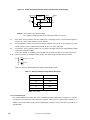
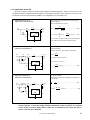
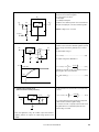
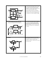
1
To our customers,
Old Company Name in Catalogs and Other Documents
On April 1st, 2010, NEC Electronics Corporation merged with Renesas Technology
Corporation, and Renesas Electronics Corporation took over all the business of both
companies. Therefore, although the old company name remains in this document, it is a valid
Renesas Electronics document. We appreciate your understanding.
Renesas Electronics website: http://www.renesas.com
April 1st, 2010
Renesas Electronics Corporation
Issued by: Renesas Electronics Corporation (http://www.renesas.com)
Send any inquiries to http://www.renesas.com/inquiry.
Notice
1.
2.
3.
4.
5.
6.
7.
All information included in this document is current as of the date this document is issued. Such information, however, is
subject to change without any prior notice. Before purchasing or using any Renesas Electronics products listed herein, please
confirm the latest product information with a Renesas Electronics sales office. Also, please pay regular and careful attention to
additional and different information to be disclosed by Renesas Electronics such as that disclosed through our website.
Renesas Electronics does not assume any liability for infringement of patents, copyrights, or other intellectual property rights
of third parties by or arising from the use of Renesas Electronics products or technical information described in this document.
No license, express, implied or otherwise, is granted hereby under any patents, copyrights or other intellectual property rights
of Renesas Electronics or others.
You should not alter, modify, copy, or otherwise misappropriate any Renesas Electronics product, whether in whole or in part.
Descriptions of circuits, software and other related information in this document are provided only to illustrate the operation of
semiconductor products and application examples. You are fully responsible for the incorporation of these circuits, software,
and information in the design of your equipment. Renesas Electronics assumes no responsibility for any losses incurred by
you or third parties arising from the use of these circuits, software, or information.
When exporting the products or technology described in this document, you should comply with the applicable export control
laws and regulations and follow the procedures required by such laws and regulations. You should not use Renesas
Electronics products or the technology described in this document for any purpose relating to military applications or use by
the military, including but not limited to the development of weapons of mass destruction. Renesas Electronics products and
technology may not be used for or incorporated into any products or systems whose manufacture, use, or sale is prohibited
under any applicable domestic or foreign laws or regulations.
Renesas Electronics has used reasonable care in preparing the information included in this document, but Renesas Electronics
does not warrant that such information is error free. Renesas Electronics assumes no liability whatsoever for any damages
incurred by you resulting from errors in or omissions from the information included herein.
Renesas Electronics products are classified according to the following three quality grades: “Standard”, “High Quality”, and
“Specific”. The recommended applications for each Renesas Electronics product depends on the product’s quality grade, as
indicated below. You must check the quality grade of each Renesas Electronics product before using it in a particular
application. You may not use any Renesas Electronics product for any application categorized as “Specific” without the prior
written consent of Renesas Electronics. Further, you may not use any Renesas Electronics product for any application for
which it is not intended without the prior written consent of Renesas Electronics. Renesas Electronics shall not be in any way
liable for any damages or losses incurred by you or third parties arising from the use of any Renesas Electronics product for an
application categorized as “Specific” or for which the product is not intended where you have failed to obtain the prior written
consent of Renesas Electronics. The quality grade of each Renesas Electronics product is “Standard” unless otherwise
expressly specified in a Renesas Electronics data sheets or data books, etc.
“Standard”:
8.
9.
10.
11.
12.
Computers; office equipment; communications equipment; test and measurement equipment; audio and visual
equipment; home electronic appliances; machine tools; personal electronic equipment; and industrial robots.
“High Quality”: Transportation equipment (automobiles, trains, ships, etc.); traffic control systems; anti-disaster systems; anticrime systems; safety equipment; and medical equipment not specifically designed for life support.
“Specific”:
Aircraft; aerospace equipment; submersible repeaters; nuclear reactor control systems; medical equipment or
systems for life support (e.g. artificial life support devices or systems), surgical implantations, or healthcare
intervention (e.g. excision, etc.), and any other applications or purposes that pose a direct threat to human life.
You should use the Renesas Electronics products described in this document within the range specified by Renesas Electronics,
especially with respect to the maximum rating, operating supply voltage range, movement power voltage range, heat radiation
characteristics, installation and other product characteristics. Renesas Electronics shall have no liability for malfunctions or
damages arising out of the use of Renesas Electronics products beyond such specified ranges.
Although Renesas Electronics endeavors to improve the quality and reliability of its products, semiconductor products have
specific characteristics such as the occurrence of failure at a certain rate and malfunctions under certain use conditions. Further,
Renesas Electronics products are not subject to radiation resistance design. Please be sure to implement safety measures to
guard them against the possibility of physical injury, and injury or damage caused by fire in the event of the failure of a
Renesas Electronics product, such as safety design for hardware and software including but not limited to redundancy, fire
control and malfunction prevention, appropriate treatment for aging degradation or any other appropriate measures. Because
the evaluation of microcomputer software alone is very difficult, please evaluate the safety of the final products or system
manufactured by you.
Please contact a Renesas Electronics sales office for details as to environmental matters such as the environmental
compatibility of each Renesas Electronics product. Please use Renesas Electronics products in compliance with all applicable
laws and regulations that regulate the inclusion or use of controlled substances, including without limitation, the EU RoHS
Directive. Renesas Electronics assumes no liability for damages or losses occurring as a result of your noncompliance with
applicable laws and regulations.
This document may not be reproduced or duplicated, in any form, in whole or in part, without prior written consent of Renesas
Electronics.
Please contact a Renesas Electronics sales office if you have any questions regarding the information contained in this
document or Renesas Electronics products, or if you have any other inquiries.
(Note 1) “Renesas Electronics” as used in this document means Renesas Electronics Corporation and also includes its majorityowned subsidiaries.
(Note 2) “Renesas Electronics product(s)” means any product developed or manufactured by or for Renesas Electronics.
User’s Manual
Usage of Three-Terminal Regulators
Document No. G12702EJAV0UM00 (10th edition)
Date Published June 2005 NS CP(K)
2000
Printed in Japan
The application circuits and the circuit constants in this document are only examples, and not intended for
use in the actual design of application systems for mass-production.
• The information in this document is current as of June 2005. The information is subject to change
without notice. For actual design-in, refer to the latest publications of NEC Electronics data sheets or
data books, etc., for the most up-to-date specifications of NEC Electronics products. Not all
products and/or types are available in every country. Please check with an NEC Electronics sales
representative for availability and additional information.
• No part of this document may be copied or reproduced in any form or by any means without the prior
written consent of NEC Electronics. NEC Electronics assumes no responsibility for any errors that may
appear in this document.
• NEC Electronics does not assume any liability for infringement of patents, copyrights or other intellectual
property rights of third parties by or arising from the use of NEC Electronics products listed in this document
or any other liability arising from the use of such products. No license, express, implied or otherwise, is
granted under any patents, copyrights or other intellectual property rights of NEC Electronics or others.
• Descriptions of circuits, software and other related information in this document are provided for illustrative
purposes in semiconductor product operation and application examples. The incorporation of these
circuits, software and information in the design of a customer's equipment shall be done under the full
responsibility of the customer. NEC Electronics assumes no responsibility for any losses incurred by
customers or third parties arising from the use of these circuits, software and information.
• While NEC Electronics endeavors to enhance the quality, reliability and safety of NEC Electronics products,
customers agree and acknowledge that the possibility of defects thereof cannot be eliminated entirely. To
minimize risks of damage to property or injury (including death) to persons arising from defects in NEC
Electronics products, customers must incorporate sufficient safety measures in their design, such as
redundancy, fire-containment and anti-failure features.
• NEC Electronics products are classified into the following three quality grades: "Standard", "Special" and
"Specific".
The "Specific" quality grade applies only to NEC Electronics products developed based on a customerdesignated "quality assurance program" for a specific application. The recommended applications of an NEC
Electronics product depend on its quality grade, as indicated below. Customers must check the quality grade of
each NEC Electronics product before using it in a particular application.
"Standard": Computers, office equipment, communications equipment, test and measurement equipment, audio
and visual equipment, home electronic appliances, machine tools, personal electronic equipment
and industrial robots.
"Special": Transportation equipment (automobiles, trains, ships, etc.), traffic control systems, anti-disaster
systems, anti-crime systems, safety equipment and medical equipment (not specifically designed
for life support).
"Specific": Aircraft, aerospace equipment, submersible repeaters, nuclear reactor control systems, life
support systems and medical equipment for life support, etc.
The quality grade of NEC Electronics products is "Standard" unless otherwise expressly specified in NEC
Electronics data sheets or data books, etc. If customers wish to use NEC Electronics products in applications
not intended by NEC Electronics, they must contact an NEC Electronics sales representative in advance to
determine NEC Electronics' willingness to support a given application.
(Note)
(1) "NEC Electronics" as used in this statement means NEC Electronics Corporation and also includes its
majority-owned subsidiaries.
(2) "NEC Electronics products" means any product developed or manufactured by or for NEC Electronics (as
defined above).
M8E 02. 11-1
2
User’s Manual G12702EJAV0UM
The mark
shows major revised points.
User’s Manual G12702EJAV0UM
3
CONTENTS
1. INTRODUCTION................................................................................................................................
5
2. BASIC STRUCTURE OF A POWER SUPPLY IC ......................................................................
5
2.1
2.2
Structure of a Bipolar IC ...........................................................................................................................
About Power Supply IC Equivalent Circuits ..............................................................................................
5
6
3. BASIC CIRCUITS OF A POWER SUPPLY IC............................................................................
7
3.1
3.2
3.3
Basic Circuits............................................................................................................................................ 7
Operating Principles of Variable Output Types......................................................................................... 11
Operating Principles of Low Saturation Types.......................................................................................... 12
4. POWER SUPPLY IC APPLICATION CIRCUITS.......................................................................... 13
4.1
4.2
Standard Circuit Connection..................................................................................................................... 13
Application Circuit Set .............................................................................................................................. 17
5. PRECAUTIONS ON APPLICATION ............................................................................................... 22
5.1
5.2
5.3
5.4
5.5
5.6
Shorting Input Pins and Ground Pins .......................................................................................................
Floating Ground Pins................................................................................................................................
Applying Transient Voltage to Input Pins..................................................................................................
Reverse Bias Between Output Pin and GND Pin .....................................................................................
Precautions Related to Low Saturation Types..........................................................................................
Thinking on Various Protection Circuits....................................................................................................
22
22
23
23
24
24
6. POWER SUPPLY IC DATA SHEET APPEARANCE AND DESIGN METHODS .................... 24
6.1
6.2
6.3
6.4
4
Absolute Maximum Ratings ......................................................................................................................
Recommended Operating Conditions.......................................................................................................
Electrical Specifications............................................................................................................................
Design Methods........................................................................................................................................
User’s Manual G12702EJAV0UM
24
24
25
28
1. INTRODUCTION
NEC Electronics produces a variety of ICs for power supplies that differ in their on-chip functions and usage.
Within these, large quantities of three-terminal regulators have come to be used to configure stabilized power supplies
easily using few external components.
However, the occurrence of unexpected irregularities when designing power supply circuits also has increased.
Therefore, this manual starts with the basic structure of the main bipolar process that is used in ICs for power supplies
and gives precautions pertaining to actual applications.
2. BASIC STRUCTURE OF A POWER SUPPLY IC
As mentioned in chapter 1, a power supply IC mainly uses a bipolar process. Understanding the structure of an IC
that uses a bipolar process also is useful for applications.
2.1 Structure of a Bipolar IC
The following elements can be made into an IC in a general bipolar process.
NPN transistor
PNP transistor
Resistor
Capacitor
Figures 2-1 through 2-3 show the structure of each.
Figure 2-1. Structure of NPN Transistor and PNP Transistor
NPN transistor
Separation region
Separation region
Collector
p
PNP transistor
n+
Base
p
Emitter
n+
n
p
n+
Separation region
Base p Collector p
n
n+
Emitter
p
p
n+
P-type substrate
User’s Manual G12702EJAV0UM
5
Figure 2-2. Structure of Resistor
Base diffused resistor
Base pinch resistor
Separation region
Separation region
Resistor
electrode
+
P-type diffusion n diffusion layer
Resistor
Pinch
layer
electrode
region
P-type diffusion Resistor
layer
electrode
n+
n
p
Epitaxial layer
Resistor fetch electrode
electrode
Separation
region
n
p
n+
p
n+
P-type substrate
Figure 2-3. Structure of Capacitor
MOS capacitor
Junction capacitor
− +
Separation region
Thin
oxide
Separation region
AI electrode
n
n+
p
n+
p
p
n
Separation region
p
n+
P-type substrate
P-type substrate
There is a point to heed in applying power supply ICs. It is that a method known as "junction separation" is used as
the method of electrically separating each of the elements above. By connecting a separation region so that it is
formed by a P-type semiconductor and is the same lowest potential as the substrate, the element region and the
separation region are electrically separated and insulated by being in (PN junction) reverse bias states. If for some
reason the potential of this separation region becomes a higher potential than the element region (for example the
NPN transistor collector region in Figure 2-1), normal operation cannot be expected since the PN junction enters a
forward bias state and the separation state between the elements cannot be maintained. For example, when using a
positive output three-terminal regulator, the GND pin always must be made a lower potential than the potential of other
pins.
2.2 About Power Supply IC Equivalent Circuits
Equivalent circuits that are shown in data sheets are so designated assuming the premise of the preceding section
(that separation regions and substrate are made the lowest potential). Be careful not to reference these when this
premise is violated.
6
User’s Manual G12702EJAV0UM
3. BASIC CIRCUITS OF A POWER SUPPLY IC
3.1 Basic Circuits
Although the basic circuits that make up a power supply IC differ according to the product type, the following
elements are necessary.
<1> Reference voltage circuit
<2> Error amplifier
<3> Active load (constant current circuit)
<4> Output stage power transistor
<5> Startup circuit
The following protection circuits also are on-chip.
<6> Overcurrent protection circuit
<7> Stable operation area (SOA or ASO) restriction circuit
<8> Overheat protection circuit
Figure 3-1 shows a block diagram of a power supply IC.
Figure 3-1. Power Supply IC Block Diagram
INPUT
Current
source
Startup
circuit
Reference
voltage
Protection
circuit
Output power
transistor
+
−
Error amplification
circuit
OUTPUT
RB
Split resistor
RA
GND
User’s Manual G12702EJAV0UM
7
The operation of each block is explained in simple terms below.
<1> Reference voltage circuit
The reference voltage circuit, which determines the output voltage of the power supply IC, is an extremely
important part within the circuit. The method for configuring this circuit is as follows.
• Band gap reference method: Use the forward characteristic between the base and emitter of the transistor.
The possibility of making the reference voltage 2 V or less is a feature of this method.
Figure 3-2 shows the principles of the band gap reference method. Figure 3-3 is a simple circuit diagram of
the band gap reference reference voltage used in the µPC7800A Series.
Figure 3-2. Band Gap Reference Circuit
V+
VREF = VBE3 + R2 ( KT ln R2 )
R3 q
R1
I
R1
VREF
R2 ∆VBE
R3
R2
Q3
Q2
VBE
Q1
∆VBE
R3
GND
The reference voltage is as follows.
VREF = VBE3 + (IC2 + IB3) x R2
= VBE3 +
R2
R3
.= VBE3 + R2
.
R3
(∆VBE) + IB3 x R2
KT
q
ln
R2
R1
............................................................................................................... (3 - 3)
The temperature coefficient is as follows.
∂VREF ∂VBE3 K R2
R2 .............................................................................................................
=
+ x
ln
(3 - 4)
q R3
∂T
∂T
R1
By optimally choosing the ratio of
obtained.
8
R2
R3
x
R2
, a temperature compensated reference voltage is known to be
R1
User’s Manual G12702EJAV0UM
Figure 3-3. (Simplified) Band Gap Reference Circuit of µPC7800A Series
VIN
VREF
GND
<2> Error amplifier
This circuit controls the output voltage by detecting and comparing the reference voltage created by the
reference voltage circuit and the resistor split output voltage. If VOUT is the output voltage and VREF is the
reference voltage (refer to Figure 3-1), the following relationship holds.
VOUT =
A
β (1 + A)
VREF ........................................................................................................................ (3 - 1)
Here, A is the open loop gain of the error amplifier and β = RA / (RA + RB).
<3> Active load (constant current circuit)
Expression (3 - 1) becomes the following if the open loop gain A of the error amplifier is sufficiently large
compared to 1.
.
VOUT =. VREF / β
A small bias current and high resistance are realized by using a constant current circuit in the error amplifier
load to make A 60 to 80 dB.
<4> Output stage power transistor
The output stage power transistor supplies current to the load. Although normally a Darlington form NPN, the
low saturation type of power supply IC uses a PNP single transistor.
User’s Manual G12702EJAV0UM
9
<5> Startup circuit
A power supply IC has an on-chip constant current circuit for use as an error amplifier load or for biasing the
reference voltage circuit. A constant current circuit, which consists of paired transistors, does not begin to
operate as long as the diode connected transistors are not in a steady bias state. A startup circuit therefore is
set up and it biases the active load at power-on to cause normal operation to begin whether the temperature of
the transistors is low or high.
<6> Overcurrent protection circuit
This is a protection circuit for preventing the load current from exceeding the current capacity of the output
stage power transistor. It restricts the base current of the output stage power transistor by biasing the current
restriction transistor more deeply in accordance with the voltage drop in the current detection resistor inserted
in the load current route.
<7> Stable operation area (SOA or ASO) restriction circuit
The stable operation area restriction circuit operates to squeeze the output current if the voltage between input
and output (voltage between the collector and emitter of the output stage power transistor) becomes large so
that the stable operation area of the output stage power transistor is not exceeded.
If the voltage difference between input and output exceeds the breakdown voltage (7 to 8 V) of a Zener diode
connected between input and output, it restricts the base current of the output stage power transistor by
biasing the current restriction transistor more deeply using the breakdown current.
Since the larger the
voltage difference between input and output the more the base current of the output stage power transistor is
restricted, the load characteristic is a "foldback" type drooping characteristic as a result.
Figure 3-4 shows the parts of a general overcurrent protection circuit and stable operation area restriction
circuit.
Figure 3-4. Sample Overcurrent Protection Circuit and Stable Operation Area Restriction Circuit
(µPC7800A Series)
Stable operation area restriction circuit
INPUT
Q16
Q17
Output transistor
Q15: Current restriction
transistor
R11: Current detection resistor
OUTPUT
10
User’s Manual G12702EJAV0UM
<8> Overheat protection circuit
The overheat protection circuit prevents destruction of the IC by cutting off output if the temperature of the chip
itself increases too much.
Figure 3-5 shows the parts of an overheat protection circuit. Q12, which is biased to the extent that it is not ON
in a normal operating state, is completely ON at 150 to 200°C accompanying a decrease in VBE when the
temperature of the chip increases. When Q12 is ON, it cuts off the output voltage by absorbing the base
current of the output stage power transistor.
Figure 3-5. Sample Overheat Protection Circuit (µPC7800A Series)
INPUT
Q16
Q17
OUTPUT
Q12: Overheat protection
transistor
GND
The overheat protection circuit is designed to operate at temperatures exceeding the absolute maximum rating
(generally 150°C). Therefore, if the overheat protection circuit has operated, the IC should be considered to
have been exposed to an abnormal state and positive use of the overheat protection circuit should be avoided
(so a separate circuit is needed to perform power supply overheat protection).
3.2 Operating Principles of Variable Output Types
A variable output type (µPC317, µPC337) differs from a fixed output voltage type in that it uses a method for
configuring an output voltage setting voltage circuit externally so that an arbitrary output voltage can be set externally.
Figure 3-6 is the block diagram of a variable output voltage type. The output voltage is controlled by comparing the
voltage between external resistors RA and RB and the reference voltage VREF in the error amplifier.
Moreover, each block is connected between INPUT and OUTPUT and the current needed in each block (circuit
operating current) is output from the OUTPUT pin.
Therefore, the outflow current from the ADJ pin becomes
negligible and its affect on the output voltage value can be ignored.
User’s Manual G12702EJAV0UM
11
Figure 3-6. Variable Output Type Block Diagram
INPUT
Current
source
Protection
circuit
+
−
Startup
circuit
Reference
voltage source
OUTPUT
VREF
ADJ
RB
RA
Output
voltage
setting
circuit
VO
3.3 Operating Principles of Low Saturation Types
All of the power supply ICs discussed so far use Darlington connected NPN type transistors in the output stage.
Therefore, the voltage difference between input and output that is needed to operate these power supply ICs cannot
be lower than the voltage between the base and emitter of the Darlington connected output transistor (0.7 V × 2 = 1.4
V). A low saturation type power supply IC makes it possible to operate with a small voltage difference between input
and output by using a PNP transistor as the output stage transistor (refer to Figure 3-7).
Figure 3-7. Differences Between General Power Supply IC and
Low Saturation Type Output Stage Configurations
(a) General power supply IC
(b) Low saturation type power supply IC
OUT
IN
IN
OUT
0.7 V
0.7 V
GND
GND
Configurations other than this are nearly identical to a general power supply IC. Figure 3-8 shows a block diagram.
12
User’s Manual G12702EJAV0UM
★ Figure 3-8. Low Saturation Type Block Diagram
INPUT
Startup
circuit
Stable operation
area restriction
circuit
Reference
voltage
circuit
Error
amplifier
Drive
circuit
Output power
transistor
OUTPUT
Overheat
protection
circuit
Overcurrent
restriction
circuit
GND
4. POWER SUPPLY IC APPLICATION CIRCUITS
4.1 Standard Circuit Connection
<1> Fixed output voltage type
Figure 4-1 shows an example of a standard circuit connection. Check the data sheet for each product type for
the values of input and output capacitors.
Figure 4-1. Sample Standard Circuit Connection (Single Power Supply Output)
CIN: Set this value according to the length of the line
D1
between the regulator and INPUT pin. Be sure to
INPUT
connect CIN to prevent parasitic oscillation. Use of
OUTPUT
Three-terminal regulator
CIN
COUT
+
a film capacitor or other capacitor with excellent
voltage
D2
and
recommended.
temperature
characteristics
is
If using a laminated ceramic
capacitor, it is necessary to ensure that CIN is 0.1
µF or higher for the voltage and temperature range
to be used.
COUT: Be sure to connect COUT to prevent oscillation and
improve excessive load regulation. Place CIN and
COUT as close as possible to the IC pins (within 2
cm). Also, use an electrolytic capacitor with low
impedance characteristics if considering use at subzero temperatures.
D1:
If the OUTPUT pin has a higher voltage than the
INPUT pin, connect a diode.
D2:
If the OUTPUT pin has a lower voltage than the
GND pin, connect a Schottky barrier diode.
Caution Make sure that no voltage is applied to the OUTPUT pin from external.
User’s Manual G12702EJAV0UM
13
Figure 4-2 is an example of a standard connection for obtaining a positive and negative power supply. The diodes
between output and GND are for preventing latchdown at startup and are absolutely necessary in the case of loads
shown by solid lines. Without the diodes, current flows in the separation regions between elements as described in
chapter 2 and the output voltage does not rise (refer to Figure 4-3).
Figure 4-2. Sample Standard Circuit Connection (Dual Power Supply Output)
Di2
+VOUT
Positive voltage
3-terminal
regulator
+VIN
CIN
Load A
Co
Di1
Load
GND
Di1'
CIN'
Co'
Negative voltage
3-terminal
regulator
−VIN
Load B
−VOUT
Di2'
CIN, CO, CIN', CO': As in the sample circuit for a single power supply load, these are needed.
Di1, Di1'
: Absolutely necessary for loads shown by solid lines, in which a load current flows from
+VOUT toward −VOUT.
This is to prevent regulator output on either side from being latched down by differences
occurring in the rise of regulator output voltage due to smoothing circuit capacitor capacity
differences or the like.
Note that these are not specifically needed in the case of only those loads shown by dashed
lines.
Di2, Di2'
: As in the sample circuit for a single power supply load, these sometimes are needed
depending on the application circuit.
14
User’s Manual G12702EJAV0UM
If the output pin becomes a lower potential than GND, the P-type separation region and n type output pin (NPN
transistor) enter a forward bias state and the "parasitic transistor" shown with dashed lines is formed. When this
occurs, it is connected to the adjacent transistors and does not operate normally.
Figure 4-3. Sample Power Supply IC Cross Section Diagram (Latchdown)
Separation Output
region
NPN transistor
NPN transistor
n p
n p
p
p
p
n
n
p
<2> Variable output voltage type
When a voltage not included in a fixed output voltage type is needed or the output voltage is to be adjusted
and used, even a fixed output voltage type can be used by floating the GND (In a low saturation type case, it
cannot do.) as described later, but voltage precision and drift become a problem. A variable output voltage
type is useful in such cases.
Figure 4-4 shows an example of the standard connection. Since a bias current for the operation of each block
inside the IC flows from INPUT to OUTPUT as described in section 3.2, be careful of the load current. By
selecting 240 Ω as R1 as in the sample standard connection even when there is no load, no problems arise
since a current of
1.25 V / 240 Ω = 5.2 mA
flows to OUTPUT.
User’s Manual G12702EJAV0UM
15
Figure 4-4. Sample Standard Connection Circuit (Variable Output Power Supply)
Input INPUT
µ PC317
ADJ
CIN
0.1µF
+
CADJ
OUTPUT
R1
240 Ω
Output
VO
D1
CO
1µF
R2
Remark This example is for a positive voltage.
For a negative voltage (µPC337), D1 and capacitor polarity are reversed.
CIN
: Since there may be oscillation if the wire leading from a smoothing circuit to a three-terminal regulator is
long (15 cm or more), add a capacitor near the input pin.
CO
: For an application in which the load current changes suddenly, add a 10 µF or more capacitor for output
voltage transient response improvement (and add 10 µF to CADJ at the same time).
CADJ
: Connecting a 10 µF capacitor parallel to R2 can improve the ripple removal rate (approximately 20 dB)
and increase oscillation stability.
In this case, diode D1 is needed for to prevent application of backward voltage on an output short circuit.
R1, R2 : These are resistors for setting the output voltage. The output voltage VO is determined as follows.
VO = 1 +
R2
R1
x VREF + IADJ x R2
R2
.
=. 1 +
x VREF
R1
Table 4-1 shows the relationship between typical output voltages and R2.
Table 4-1. Settings of Output Voltage Setting Resistor R2
Output Voltage VO (V)
R2 Setting
Note
2.5
240
5.0
720
12
2064
24
4368
30
5520
(Ω)
Note TYP. values
<3> Low saturation type
The standard method of use is the same as for a general fixed output voltage type (see Figure 4-1). However,
the capacitor connected to the output must have a greater capacity than in a general power supply IC. In
addition, note that the output voltage cannot be adjusted by inserting a resistor or the like in the GND pin as
described later.
16
User’s Manual G12702EJAV0UM
4.2 Application Circuit Set
This circuit set mainly is filled in for positive output voltage three-terminal regulators. However, the circuits also can
be applied to negative voltage three-terminal regulators by changing the polarity of parts employed. In the case of the
circuit which has connected an element to GND pin, it is inapplicable to a low saturation type.
Drives the base of an external transistor using a three-
1. High output current circuit
terminal regulator.
(without short circuit protection)
Here R1 is determined as follows.
VBE1
VIN
IOUT
Q1
IO VOUT
R1 =
IOUT
IREG(MAX.) −
…………………….…. (4.1)
hFEI(MIN.)
IREG
6Ω
IN
R1
OUT
GND
IO = hFE1(MIN.)
IREG(MAX.) −
C2
C1
VBE1
R1
+ IREG(MAX.) … (4.2)
In this circuit, the output current has an actual range that
is 5 to 6 times the three-terminal regulator rating.
2. High output current circuit
This is an expansion of circuit 1. Current detection is
performed using R2.
(with short circuit protection)
Therefore, since the current at Q1 is restricted by
VIN
R2
I1
Q1
IO VOUT
IREG
R1
6Ω
VBE2
I1(MAX.) =
R2
the output current is as follows.
Q2
IN
R1
IO(MAX.) = I1(MAX.) + IREG(MAX.)
OUT
GND
3. High output current circuit
VBE2
=
C2
C1
+ IREG(MAX.) …..………..……….….…. (4.3)
R2
D1 cancels VBE at Q1.
Q1 and three-terminal current distribution is determined
(with short circuit protection)
by R1 and R2.
VIN
R2
R1 0.4 Ω
2Ω
I1
Q1
IO VOUT
I1
IREG
IO(MAX.) =
IN
C1
R1
=
IREG
R3 6 Ω
D1
R2
OUT
GND
……………………….…………….…… (4.4)
R1 + R2
R1
x IREG(MAX.) …………………..….. (4.5)
C2
Caution Absolutely do not connect output pins in parallel to increase the current capacity of a threeterminal regulator. If the output voltage becomes unbalanced, certain ICs operate in a restricted
current vicinity and current hardly flows in certain ICs, and furthermore the current may flow in
reverse. Also refer to 15. Wired OR.
User’s Manual G12702EJAV0UM
17
4. High input voltage circuit
This circuit can be used when the input voltage exceeds
the rating.
VIN
Q1
IN
IOUT(MAX.) + IBIAS(MAX.)
VOUT
OUT
GND
R1
VIN − VZD
R1 =
IOUT
………………….… (4.6)
hFE1(MIN.)
Moreover, if the load current changes little, a resistor can
C1
C2
IBIAS
be used.
ZD
5. High input, high output voltage circuit
Using the fact that the current flowing out from the GND
(without short circuit protection)
pin of the three-terminal regulator is practically constant,
add Zener diode to the GND pin to raise only the Zener
portion of the voltage. R1 supplies idling to the Zener. It
VIN
IN
VOUT
OUT
GND
C1
also is possible to use a resistor, but this is inferior to the
Zener from a stability standpoint.
D is needed as load short circuit protection. In addition,
R1
C2
D
the input voltage must be set within a range that holds
the voltage difference between input and output to the
ratings even on a short circuit.
ZD
6. High input, high output voltage circuit
This circuit combines circuits 4 and 5. The circuit made
Note
)
(with short circuit protection
up of Q1, Q2, and D1 is a preregulator.
The output voltage is as follows.
VIN
R1
4.7 kΩ
Q2
IN
R2
1 kΩ
Q1
VO(REG) VOUT
OUT
GND
VOUT = VO(REG) + VZD ..…………………………....... (4.7)
D2 protects against reverse bias in the GND and OUT
pins on a load short circuit.
C1
C2
D2
Note
D1 or ZD must be selected so that the voltage
difference between input and output of the three-
D1
terminal regulator is kept within ratings even on a
ZD
load short circuit.
In addition, D2 must have low forward voltage.
18
User’s Manual G12702EJAV0UM
7. Remote shutdown circuit
Control the output voltage using a preregulator set up
ahead of the three-terminal regulator.
The control input is as follows.
D1
At H: Output
At L: Output interruption
VIN
Q1
IN
R1
VOUT
OUT
GND
In addition, D1 is added to prevent reverse bias between
the input and output pins of the three-terminal regulator.
Remark H: High level, L: Low level
C1
R2
C2
Control
Q2
R3
8. Slow startup circuit (without short circuit protection)
This circuit moderates the rise time of the output voltage.
At power-on, this is the three-terminal regulator's specific
VIN
IN
VOUT
VO(REG)
OUT
GND
D1
C1
VO1 = VO(REG) .........…………………………......... (4.8)
R3
R1
Q1
The output voltage after stabilization is
C2
VOUT
value.
The initial output voltage is
R2
IBIAS
output voltage, after which it gradually rises to its final
VO2 = VO(REG) + R1
VO(REG)
…………. (4.9)
R2
Furthermore, the delay can be represented as follows if
VO final value
IBIAS +
expecting up to 99% of the final value.
VO(REG)
T
−CR ln 0.01 [s] ........………………………... (4.10)
Delay time T
Power on
Time
9. Variable output voltage circuit
The Zener diode in the circuit shown in 5 is replaced by
(without load short circuit protection)
VIN
IN
C1
VO(REG)
OUT
GND
C2
IBIAS
a resistor.
VOUT
R2
VOUT = VO(REG) + R1
IBIAS +
VO(REG)
R2
………… (4.11)
Use a voltage difference between input and output that
is within the three-terminal regulator ratings.
D1
R1
For a load short circuit or capacity load, the diode shown
using dashed lines is needed and in particular a low
forward voltage is needed.
Note that applications using the variable output three-terminal
regulator µPC317 are superior in output voltage precision and
stability.
User’s Manual G12702EJAV0UM
19
10. Variable output voltage circuit
Splits the fixed output voltage VO(REG) of the threeterminal regulator using R4 and R5 and compares with
(0.5 to 10 V, without short circuit protection)
the output voltage VOUT value split using R1 and R2.
The output voltage can be represented as follows.
10 µ F
+
µ PC7805A
+VIN
C1
VOUT
IN
OUT
GND
R4
0.1 µ F
VO(REG) 910 Ω
R5
9.1 kΩ −
R1
+
R2
µ PC741
−VIN R3
10
kΩ
VOUT =
R4
R4 + R5
× VO(REG) ×
R1 + R2
R1
…………. (4.12)
C2
0.1 µ F
10 µ F
+
RD6.2EB
This is analogous to the circuits shown in 5 and 8. Since
11. Variable output voltage circuit (7 to 30 V)
it uses op amplifier µPC741 with a single power supply,
the lowest value of the output voltage can be no lower
than the sum of the output saturated voltage of the
VIN
IN
VOUT
OUT
GND
−
C1
µ PC741
R1 10 kΩ
+
µPC741 and the output voltage of the three-terminal
regulator.
C2
R2
A tracking regulator is configured using a power
12. Tracking regulator circuit
transistor with one positive voltage three-terminal
regulator.
+VIN
IN
+VOUT
OUT
GND
The positive voltage is the fixed voltage of the threeterminal regulator. The negative voltage can be
changed arbitrarily by the split ratio of R1 and R2.
C1
C2
Thus the negative voltage output is as follows.
R1
− VOUT =
C3
µ PC741
D1 protects against reverse bias between the base and
emitter of the transistor at power-on.
R2
D1
−VOUT
Tf1
20
x VOUT ……………………………. (4.13)
−
+
−VIN
R2
R1
User’s Manual G12702EJAV0UM
13. Tracking regulator circuit
This power supply has superior tracking characteristics
due to using an operational amplifier and one positive
and one negative voltage three-terminal regulator.
The GND pin of each three-terminal regulator is driven in
+ VIN
IN
+ VOUT
OUT
GND
C1
C2
+
C3
C4
IN
− VIN
GND
OUT
R1
µPC741
−
common by the operational amplifier output.
Favorable tracking characteristics are obtained by
making R1 = R2. Moreover, bias current errors also can
be canceled if the resistor R1//R2 is added between the
non-inverting pin of the operational amplifier and GND.
R1
R2
R2
− VOUT
14. Positive and negative dual power supply circuit
This is a positive and negative dual power supply that
(using positive voltage three-terminal regulators)
uses two positive voltage three-terminal regulators.
D1 and D2 are low forward voltage diodes that are
absolutely necessary. They prevent output voltage
IN
+ VOUT
OUT
GND
pulldown due to discrepancies in the startup timing of
each regulator.
D1
IN
GND
OUT
GND
D2
− VOUT
15. Wired OR
When connecting the outputs of two or more threeterminal regulators, do it so that voltage from outside is
not added to the regulator output at D1 and D3.
D1
VIN1
VOUT
D2 and D4 are connected to compensate for the lowering
of output by D1 and D3.
D2
D3
VIN2
D4
User’s Manual G12702EJAV0UM
21
5. PRECAUTIONS ON APPLICATION
Do not use a three-terminal regulator under temperature conditions or voltage conditions that exceed the ratings.
Other precautions that are specific to three-terminal regulators are shown below.
5.1 Shorting Input Pins and Ground Pins
When a capacitor with a large capacity is connected to the load of a three-terminal regulator, if the input pin is
shorted to GND or the power supply is turned OFF, the voltage of the capacitor connected to the output pin is applied
between the output and input pins of the three-terminal regulator.
Figure 5-1
(a)
(b)
Discharge current
VOUT
IN
IN
OUT
VOUT
+
OUT
GND
+
GND
The withstand voltage between the output and input pins of a three-terminal regulator is approximately 0.7 V for a
low current with the output transistor base-emitter voltage.
Therefore, a diode like the one in Figure 5-1 (b) is effective against the reverse bias of the input and output pins.
Figure 5-1 (b) is for a positive voltage regulator. The diode direction is reversed for negative voltage.
5.2 Floating Ground Pins
Do not make the GND pin of a three-terminal regulator floating in the operating state. If it is made floating, an input
voltage that has not been stabilized is output unchanged. This is because the output stage power transistor is biased
by an overvoltage protection Zener or current mirror transistor leakage current. Since IC internal overheat protection
and the like do not operate normally in this case, there is a possibility of destruction if the load is short-circuited or on
an overload.
Be particularly careful when using a socket.
22
User’s Manual G12702EJAV0UM
5.3 Applying Transient Voltage to Input Pins
A three-terminal regulator is destroyed if a higher voltage than the rating or a voltage more than 0.5 V lower than
the GND pin is applied to the input line. In cases in which such voltages are superimposed on the line, add a surge
suppressor using a Zener diode or the like.
Figure 5-2
(a)
+ VIN
(b)
IN
R
OUT
L
+ VO
IN
GND
GND
D1
C
OUT
C
ZD
5.4 Reverse Bias Between Output Pin and GND Pin
Figure 5-3
(a)
+ VIN
IN
(b)
VOUT
OUT
GND
IBIAS
External protection diode
ZD
VZ
In the sample application shown in Figure 5-3 (a), the voltage of the Zener diode is applied between the output and
GND pins of the three-terminal regulator when the load is short-circuited.
Inside the three-terminal regulator, a diode like that shown in Figure 5-3 (b) apparently is formed, but if a current
flows in this part, the three-terminal regulator is sometimes destroyed. Therefore, when using a GND like that shown
in Figure 5-3 (a) in a floating state, it is necessary to add a low forward voltage diode from the GND pin of the threeterminal regulator toward the output pin.
User’s Manual G12702EJAV0UM
23
5.5 Precautions Related to Low Saturation Types
Since a low saturation type of power supply IC uses a PNP transistor in the output stage, particular care is needed.
In a low input state before the output voltage enters regulation state (such as at startup), a large circuit current flows
because the output stage transistor is saturated. Depending on the product, the circuit current is decreased at startup
by an on-chip rushing current prevention circuit, but even in this case a relatively large circuit current flows compared
to normal operation (For details, refer to the "Circuit operating current at startup IBIAS(S)" rating of each product). Thus,
care is needed in the following matters.
• On startup, be careful of the output capacity of the power supply on the input side and the output impedance,
since a circuit operating current flows in the input superimposed on the load current.
• It is not possible to adjust the output voltage by inserting a resistor or the like in the GND. This is because the
circuit operating current increases at startup.
Be sure to connect a low impedance type capacitor to the output to increase stability against abnormal oscillation.
5.6 Thinking on Various Protection Circuits
NEC Electronics power supply ICs, which have on-chip overcurrent protection circuits, stable operation area
restriction circuits, and overheat protection circuits, are very difficult to destroy in their normal operating state.
Nonetheless, you should not design circuits that put too much confidence in these protection circuits. These
protection circuits are for protection against sudden accidents. To the best of your ability, avoid operating protection
circuits for long stretches of time. In particular, be careful using the overheat protection circuit since this is like
operating at a temperature exceeding the absolute maximum rating.
6. POWER SUPPLY IC DATA SHEET APPEARANCE AND DESIGN METHODS
6.1 Absolute Maximum Ratings
This item shows values that must not be exceeded even momentarily under any usage conditions or test conditions.
Moreover, it is a mistake to think that use at the absolute maximum ratings is possible. Design should be performed
so that even in an abnormal state the equipment being considered leaves room for the absolute maximum ratings.
In addition, it is assumed that GND is the lowest potential in the case of a positive output power supply and that
INPUT is the lowest potential in the case of a negative output power supply (see chapter 2).
6.2 Recommended Operating Conditions
If used under these conditions, it is possible to obtain output voltage precision as expected.
criterion for selecting a power supply IC.
24
User’s Manual G12702EJAV0UM
Think of this as a
6.3 Electrical Specifications
NEC Electronics guarantees the minimum values and maximum values of electrical characteristics at the time of
shipment. Therefore, whether or not it is possible to satisfy the specifications of the power supply to be designed must
be determined by adequately investigating each rating and condition in each item of the electrical characteristics.
Each item of the electrical characteristics is described below (Since the explanations below are mainly for positive
output power supply ICs, reread them while reversing polarities for negative power supply ICs).
<1> Output voltage VO
This item is the most important rating in using a power supply IC. Pay attention to measurement conditions. If
power supply specifications are within this range of conditions, the expected precision (for example ±5%) is
obtained (see Figure 6-1).
Figure 6-1. Output Voltage Conceptualization (For µPC7805AHF) Guaranteed Range Inside Broken Lines
5.4
Output voltage VO (V)
5.2
5.0
4.8
VIN = 10 V
IO = 5 mA
−50
0
50
100
150
Junction temperature TJ (°C)
<2> Input stability REGIN
When the input voltage increases, the output voltage also increases. This item shows how much the output
voltage changes when the input voltage VIN is varied within the measured conditions. As shown in Figure 6-2,
output voltage changes nearly linearly with respect to input voltage. Therefore, it is possible to infer how much
the output voltage will change from the initial period when the initial input voltage is changed to a given input
voltage.
User’s Manual G12702EJAV0UM
25
Figure 6-2. Input Stability REGIN Conceptualization (For µPC7805AHF, VIN = 10 V Standard)
+30
+10
REGIN TYP.
REGIN MAX.
Input stability REGIN (mV)
+20
0
−10
TA = 25°C
IO = 500 mA
−20
0
5
10
15
20
25
Input voltage VIN (V)
<3> Load stability REGL
Whereas REGIN is the change in output voltage with respect to input voltage, load stability REGL shows the
change in output voltage with respect to load current (output current). When load current increases, output
voltage decreases nearly linearly. The output voltage for an arbitrary load current can be inferred in the same
way as REGIN (see Figure 6-3).
26
User’s Manual G12702EJAV0UM
Figure 6-3. Load Stability Conceptualization (For µPC7805AHF, IO = 500 mA)
−10
REGL MAX.
0
REGL TYP.
Load stability REGL (mV)
+10
−20
−30
TA = 25°C
VIN = 10 V
0
0.5
1.0
1.5
Output current IO (A)
<4> Circuit operating current IBIAS
This is the bias current needed for each internal block of a power supply IC to operate. It flows from input
toward GND. Applications that adjust output voltage by inserting a resistor in GND take this item into account.
<5> Circuit operating current change ∆IBIAS
This shows the change in IBIAS when the input voltage or load current changes.
<6> Ripple removal rate R • R
The ripple voltage that appears in the output when a 120 Hz sine wave (minimum value and maximum value
of sine wave are noted in measured conditions) is input in the input is represented by the following expression.
R • R = 20 log (VIN/VOripple) [dB]
If the frequency increases, R • R decreases mainly due to the frequency characteristics of the internal error
amplifier of the IC.
<7> Output noise voltage Vn
This shows the noise that occurs inside a power supply IC (mainly thought to be thermal noise).
User’s Manual G12702EJAV0UM
27
<8> Peak output current IOpeak
This is the current at which the overcurrent protection circuit operates. It is defined as the output current when
the output voltage is lowered by 2 or 5% from its initial value.
As described in chapter 3, the overcurrent protection circuit operates together with the stable operation area.
Moreover, note that IOpeak decreases as temperature increases (negative temperature characteristic). Figure
6-4 shows the IOpeak - (VIN - VO) characteristics of the µPC7800A Series. For a nonlinear load such as a motor
or lamp, select a power supply IC that has sufficient leeway (50% or less of normal characteristic graph).
<9> Output short circuit current IOshort
This is the current that flows when output is short-circuited to GND. Since most NEC Electronics power
supply ICs have an on-chip stable operation area restriction circuit, the following relation holds if input voltage
is high.
IOshort < IOpeak
Like IOpeak, IOshort displays a negative temperature characteristic.
Refer to Figure 6-4 for temperature
characteristics of the output short circuit current and changes with respect to input voltage.
Figure 6-4. Sample IOpeak Characteristics (µPC7800A Series)
IOpeak - (VIN - VO) characteristic
Peak output current IOpeak (A)
3.0
2.5
2.0
TJ =
1.5
0°C
75°
C
1.0
125
25°
C
°C
0.5
0
5
10
15
20
25
30
35
Voltage difference between input and output VIN − VO (V)
6.4 Design Methods
(A) Input circuit design
Determine the capacity of a smoothing capacitor of an input circuit using an O.H. Shade graph or simulator so
that the minimum value of the input voltage is not lower than the measurement conditions of output voltage.
At this time, connect a film capacitor between input and GND of the power supply IC separate from the
smoothing capacitor to prevent abnormal oscillation (refer to the data sheet of each product type for capacitor
values).
28
User’s Manual G12702EJAV0UM
(B) Output circuit design
Check whether the load current used is a current no greater than the peak output current.
Connect a capacitor for abnormal oscillation prevention between output and GND of the power supply IC. If
transient load stability becomes a problem, make sure the capacitor is connected in parallel.
(C) Radiation design
The junction temperature can be calculated using the following expression.
TJ = (Rth(J-C) + θC-HS + θHS) x PD + TA................................................................................................ (6.1)
Rth(J-C) : Thermal resistance between junction and case
θC-HS
: Contact thermal resistance (includes thermal resistance of insulation sheet when using
θHS
: Thermal resistance of radiator
insulation sheet)
PD
: Internal power consumption of IC (PD = (VIN - VO) x IO + VIN x IBIAS)
TA
: Ambient operating temperature
Expression (6.1) is the calculation expression when using a radiator. When not using a radiator, such as in
the µPC78L00J Series, use the following expression.
TJ = Rth(J-A) x PD + TA ...................................................................................................................... (6.2)
Use the values in the data sheets for Rth(J-C) and Rth(J-A) in expressions (6.1) and (6.2).
Since TJ, Rth(J-C), PD, and TA are given, find the thermal resistance of the radiator θHS from them using
expression (6.1). Figure 6-5 shows the thermal resistance of an aluminum board. Since the makers of
radiators produce radiators suited to power supply ICs, also consult the radiator maker.
Figure 6-5. Thermal Resistance of Aluminum Board
Thermal resistance of
radiation board θ HS (°C/W)
100
50
20
t = 1.5 mm
t = 3 mm
10
5
2
1
10
20
50 100 200
500 1000
Surface area of radiation board A (cm2)
If TJ is not within the design values, return to (A) or (B) and recalculate. An example of radiator design is
shown next.
User’s Manual G12702EJAV0UM
29
<1> Design objectives
Positive power supply using µPC7805AHF
Maximum output current
IO max. = 0.6 (A)
Maximum voltage difference between input and output
VDIF max. = 6 (V)
Maximum ambient operating temperature
TA max. = 60 (°C)
Maximum junction temperature
TJ max. = 100 (°C)
<2> Radiation board thermal resistance calculation
In a used state, the junction temperature TJ is the following.
TJ = (Rth(J-C) + θC-HS + θHS) x PD + TA ..................................................................................................... (6.3)
Rth(J-C) : Thermal resistance between junction and case
θC-HS : Thermal resistance between case and radiator
θHS
: Thermal resistance of radiator
PD
: Power consumption
Here, TJ max. = 100 (°C), TA max. = 60 (°C), θC-HS << 1 (°C/W), and Rth(J-C) = 5.0 (°C/W)
.
By substituting PD max. =. VDIF max. × IO max. = 3.6 (W) in expression (6.3), find the thermal resistance θHS needed
in the radiator.
θHS =
T J – TA
PD
– Rth(J-C) – θC-HS
= 6.1 (°C/W) ................................................................................................................................... (6.4)
<3> Determination of size of radiation board
From expression (6.4), the design objectives can be satisfied using a radiator of 6.1 (°C/W).
Figure 6-5 shows the relationship between the thickness, surface area, and thermal resistance of an aluminum
board.
By using a 3 mm thick 60 cm2 aluminum board here, we know that the radiation board will have the necessary
thermal resistance.
(Sample use without radiator)
The junction temperature TJ in the used state when not installing a radiation board is the following.
TJ = Rth(J-A) x PD + TA ....................................................................................................................... (6.5)
Rth(J-A) : Thermal resistance between junction and ambient air (still air ..... natural convection)
PD
: Power consumption
TA
: Ambient operating temperature
Setting TJ to 100°C or less in the used state is recommended.
30
User’s Manual G12702EJAV0UM
Precautions when installing in a radiator
• Make the convexity or concavity of the part installation surface of the radiator 0.05 mm or
less.
• Spread silicon grease to a uniform thickness between the radiator and part. Determine
the kind of grease on consulting the maker of the radiator.
• Painting the radiator black increases its effectiveness in radiating heat. However, if it is
close to a heat source, it has the reverse effect of absorbing heat.
• Use one of the insulating board bushings shown in Table 6-2.
• Cut a screw in a radiator and absolutely do not use self-tapping screws to install one.
When installing a radiator, if the tightening torque of a screw is too great, the fins can be distorted and the IC
damaged. Drive screws using a torque driver that can manage the tightening torque.
Table 6-1. Three-Terminal Regulator Tightening Torque
Markings
Tightening torque (N•m)
TO-126
0.2 to 0.4
TO-220
0.3 to 0.5
MP-45G
0.3 to 0.5
Figure 6-6. Standard Installation Method for Radiation Board Insulation
3 M screw
Flat washer
3 M screw
Flat washer
Insulating board
Insulating bushing
Spring washer
3 M nut
Radiation board
Radiation board
Flat washer
Spring washer
3 M nut
MP-45G
TO-220
Table 6-2. Recommended Insulating Bushings and Insulating Board
Code No.
Product Name
Quality of Materials
Material
Incombustibility
Color
Insulating bushing
B-24
25K bushing U
Gelanex 3310
Light brown
Insulating board
S-7
MP-25 insulating board A
Polyester
Colorless, transparent
User’s Manual G12702EJAV0UM
Grade
UL 94V-0
−
31
For further information,
please contact:
NEC Electronics Corporation
1753, Shimonumabe, Nakahara-ku,
Kawasaki, Kanagawa 211-8668,
Japan
Tel: 044-435-5111
http://www.necel.com/
[North America]
[Europe]
[Asia & Oceania]
NEC Electronics America, Inc.
2880 Scott Blvd.
Santa Clara, CA 95050-2554, U.S.A.
Tel: 408-588-6000
800-366-9782
http://www.necelam.com/
NEC Electronics (Europe) GmbH
Arcadiastrasse 10
40472 Düsseldorf, Germany
Tel: 0211-65030
http://www.ee.nec.de/
NEC Electronics Hong Kong Ltd.
12/F., Cityplaza 4,
12 Taikoo Wan Road, Hong Kong
Tel: 2886-9318
Sucursal en España
Juan Esplandiu, 15
28007 Madrid, Spain
Tel: 091-504-2787
Seoul Branch
11F., Samik Lavied’or Bldg., 720-2,
Yeoksam-Dong, Kangnam-Ku,
Seoul, 135-080, Korea
Tel: 02-558-3737
Succursale Française
9, rue Paul Dautier, B.P. 52
78142 Velizy-Villacoublay Cédex
France
Tel: 01-3067-5800
NEC Electronics Shanghai Ltd.
Room 2509-2510, Bank of China Tower,
200 Yincheng Road Central,
Pudong New Area, Shanghai P.R. China P.C:200120
Tel: 021-5888-5400
Filiale Italiana
Via Fabio Filzi, 25/A
20124 Milano, Italy
Tel: 02-667541
NEC Electronics Taiwan Ltd.
7F, No. 363 Fu Shing North Road
Taipei, Taiwan, R. O. C.
Tel: 02-2719-2377
Branch The Netherlands
Boschdijk 187a
5612 HB Eindhoven
The Netherlands
Tel: 040-2445845
NEC Electronics Singapore Pte. Ltd.
238A Thomson Road,
#12-08 Novena Square,
Singapore 307684
Tel: 6253-8311
Tyskland Filial
P.O. Box 134
18322 Taeby, Sweden
Tel: 08-6380820
United Kingdom Branch
Cygnus House, Sunrise Parkway
Linford Wood, Milton Keynes
MK14 6NP, U.K.
Tel: 01908-691-133
Document No. G12702EJAV0UM00 (10th edition)
G04.1
Date Published June 2005 NS CP(K)
C
2000
Printed in Japan