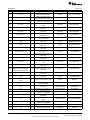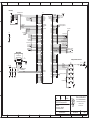
1
Tiva™ TM4C123G Development Board
User's Guide
Literature Number: SPMU357B
August 2013 – Revised March 2014
Contents
1
DK-TM4C123G Overview
1.1
1.2
1.3
1.4
2
Hardware Description
2.1
2.2
2.3
2.4
2.5
3
...................................................................................................... 4
Kit Contents ..................................................................................................................
Using the DK-TM4C123G ..................................................................................................
Features ......................................................................................................................
Specifications ................................................................................................................
5
5
5
6
.......................................................................................................... 7
Microcontroller, USB OTG, User/Navigation Switches, User LED, and GPIO Headers (Schematic page
1) .............................................................................................................................. 8
2.1.1 Microcontroller ...................................................................................................... 8
2.1.2 USB Host/Device/OTG ............................................................................................ 8
2.1.3 User Switches and User LED .................................................................................... 9
2.1.4 GPIO Headers ...................................................................................................... 9
Data Logger, Motion Sensor, Temperature Sensors, CAN Transceiver, OLED, and SD Card
(Schematic page 2) ......................................................................................................... 9
2.2.1 Data Logger ......................................................................................................... 9
2.2.2 4-Channel Analog Measurement ................................................................................. 9
2.2.3 9-Axis Motion Sensor ............................................................................................ 10
2.2.4 Temperature Sensors ............................................................................................ 11
2.2.5 MCU Running Current ........................................................................................... 12
2.2.6 CAN Transciever ................................................................................................. 12
2.2.7 OLED Display ..................................................................................................... 13
2.2.8 SD Card ............................................................................................................ 13
Hibernate, Current Shunts, Power Supplies, Reset and Crystals (Schematic page 3) .......................... 13
2.3.1 Hibernate .......................................................................................................... 13
2.3.2 Current Shunt Resistors ......................................................................................... 14
2.3.3 Clocking ............................................................................................................ 15
2.3.4 Reset ............................................................................................................... 15
2.3.5 Power Supplies and Jumper .................................................................................... 15
Debug and Virtual COM Port (Schematic Page 4) .................................................................... 16
2.4.1 In-Circuit Debug Interface (ICDI) ............................................................................... 16
2.4.2 Virtual COM Port ................................................................................................. 17
Wireless Evaluation Module Connectors (Schematic Page 5) ...................................................... 17
Software Development
....................................................................................................... 18
Software Description ......................................................................................................
Source Code ...............................................................................................................
Tool Options ................................................................................................................
Programming the DK-TM4C123G Board ...............................................................................
18
18
18
19
20
E
........................................................................................................
Bill of Materials (BOM) .......................................................................................................
References .......................................................................................................................
Schematics .......................................................................................................................
Revision History ................................................................................................................
2
Contents
3.1
3.2
3.3
3.4
A
B
C
D
Component Locations
21
24
25
26
SPMU357B – August 2013 – Revised March 2014
Submit Documentation Feedback
Copyright © 2013–2014, Texas Instruments Incorporated
www.ti.com
List of Figures
1-1.
Board Picture ................................................................................................................
4
2-1.
DK-TM4C123G Development Board Block Diagram ...................................................................
7
2-2.
Can Diagram ...............................................................................................................
2-3.
Debug Out ..................................................................................................................
16
A-1.
DK-TM4C123G Component Locations (Top View)
...................................................................
DK-TM4C123G Component Locations (Bottom View) ...............................................................
20
A-2.
12
20
List of Tables
1-1.
DK-TM4C123G Specifications
............................................................................................
6
2-1.
USB Host/Device/OTG Signals ...........................................................................................
8
2-2.
User Switches and User LED Signals ....................................................................................
9
2-3.
4-Channel Analog Measurement Signals ................................................................................
9
2-4.
9-axis Motion Sensor Signals ............................................................................................
10
2-5.
Temperature Sensor Signals.............................................................................................
11
2-6.
Linear Transfer Functions for Common Temperature Ranges ......................................................
11
2-7.
Microcontroller Running Current Signals ...............................................................................
12
2-8.
CAN Transceiver Signals .................................................................................................
12
2-9.
OLED Display Signals ....................................................................................................
13
2-10.
SD Card Signals ...........................................................................................................
13
2-11.
Power Requirements ......................................................................................................
15
2-12.
Breakout Requirements...................................................................................................
15
2-13.
..............................................................................
Virtual COM Port Signals .................................................................................................
Wireless Evaluation Module Signals ....................................................................................
Revision History ...........................................................................................................
2-14.
2-15.
E-1.
In-Circuit Debug Interface (ICDI) Signals
SPMU357B – August 2013 – Revised March 2014
Submit Documentation Feedback
Copyright © 2013–2014, Texas Instruments Incorporated
List of Figures
16
17
17
26
3
Chapter 1
SPMU357B – August 2013 – Revised March 2014
DK-TM4C123G Overview
The Tiva TM4C123G development kit is an evaluation platform for the Tiva TM4C123GH6PGE ARM®
Cortex™-M4-based series microcontrollers. The development board highlights the TM4C123GH6PGE
microcontroller's USB 2.0 On-The-Go/Host/Device (OTG/Host/Device) interface, 12-bit Analog-to-Digital
Converter (ADC), Real-Time Clock (RTC), and battery-backed Hibernation module. Figure 1-1 shows a
photo of the DK-TM4C123G.
JTAG
Header
OLED
Graphics
Display
Power Select USB Connector
Jumper
(Power/ICDI)
User/
Navigation
Switches
SELECT/
WAKE
Button
Power
LED
INA198
Current Shunt
Amplifier
and Current
Shunt
Resistors
8-Position Screw Terminal Block
for Analog Measurement and CAN
Tiva C Series
TM4C123GH6PGE
Microcontroller
9-axis
Digital Motion Sensor
Reset
Switch
USB Connector
(Host/Device/
OTG)
External
Temperature
Sensor
User
LED
microSD
Card Slot
CAN
Transceiver
Figure 1-1. Board Picture
All trademarks are the property of their respective owners.
4
DK-TM4C123G Overview
SPMU357B – August 2013 – Revised March 2014
Submit Documentation Feedback
Copyright © 2013–2014, Texas Instruments Incorporated
Kit Contents
www.ti.com
1.1
Kit Contents
The DK-TM4C123G Development Kit comes with the following:
• DK-TM4C123G development board
• On board In-Circuit Debug Interface (ICDI)
• Cables:
– Two USB Micro-B plug to USB-A plug cables (one for debug)
– USB Micro-A plug to USB-A receptacle cable
• 3-V CR2032 lithium coin-cell battery
• USB Flash drive containing:
– Complete documentation
– TivaWare™ for C Series Peripheral Driver Library and example source code
– A supported evaluation version of all of the following:
• Texas Instruments’ Code Composer Studio™ IDE
• Keil™ RealView® Microcontroller Development Kit (MDK-ARM)
• IAR Embedded Workbench® development tools
• Sourcery CodeBench™ development tools (time limited)
• GCC
1.2
Using the DK-TM4C123G
The recommended steps for using the DK-TM4C123G development kit are:
1. Follow the README First document included in the kit. The README First document will help get
the DK-TM4C123G development board up and running in minutes.
2. Use your preferred ARM tool-chain and the Tiva Peripheral Driver Library to develop an
application. Software applications are loaded using the on-board In-Circuit Debug Interface (ICDI).
See Chapter 3, Software Development, for the programming procedure. The TivaWare Peripheral
Driver Library User's Guide contains specific information on software structure and function.
3. Customize and integrate the hardware to suit an end application. This user's manual is an
important reference for understanding circuit operation and completing hardware modification.
1.3
Features
The DK-TM4C123G development kit includes the following features:
• Tiva TM4C123GH6PGE Microcontroller
• Data logger demo application
• 9-axis (accelerometer + gyro + compass) motion sensor
• 2 Analog temperature sensors
– External TMP20 temperature sensor
– Internal microcontroller temperature sensor
• Controller Area Network (CAN) transceiver
• 8 screw terminals
– 4 analog inputs (0-20 V)
– Power
– Ground
– CAN-High
– CAN-Low
SPMU357B – August 2013 – Revised March 2014
Submit Documentation Feedback
Copyright © 2013–2014, Texas Instruments Incorporated
DK-TM4C123G Overview
5
Specifications
•
•
•
•
•
•
•
•
•
•
•
•
•
1.4
www.ti.com
Microcontroller current shunt amplifier
96 x 64 color OLED display
USB Micro-AB connector for Host/Device/OTG
microSD card slot
5 navigation switches
User LED
Precision 3.0V reference
Connectors for Wireless Evaluation Modules
Available I/O brought out to headers on 0.1" grid
Debug
– In-Circuit Debug Interface (ICDI)
– Standard 10-pin JTAG header (debug-out capable)
Shunt resistors to measure current on VBAT and VDD
Coin cell backup battery for Hibernate mode
Reset button
Specifications
Table 1-1 shows the specifications for the DK-TM4C123G development board.
Table 1-1. DK-TM4C123G Specifications
Parameter
6
Value
Board supply voltage
4.75-5.25V
Dimensions
6.0" x 2.25" x 0.65" (LxWxH)
RoHS status
Compliant
DK-TM4C123G Overview
SPMU357B – August 2013 – Revised March 2014
Submit Documentation Feedback
Copyright © 2013–2014, Texas Instruments Incorporated
Chapter 2
SPMU357B – August 2013 – Revised March 2014
Hardware Description
The DK-TM4C123G development board includes a Tiva TM4C123GH6PGE microcontroller and an
integrated In-Circuit Debug Interface (ICDI) as well as a range of useful peripheral features (see the block
diagram in Figure 2-1). This chapter describes how these peripherals operate and interface to the
microcontroller.
Wireless Evaluation
Module Connector
Power
Select
Jumper
Analog
CANL
CANH
Screw
Terminals
Host
3.0V
Ref.
Battery
3.3V
LDO
+3.3V
Dual
Power
Switch
13V
Boost
MicroSD
Card Slot
SSI0
AIN3
AIN2
AIN1
AIN0
USB
+13V
96 x 64
Color OLED Display
SSI2
VREFA+
TM4C123GH6PGE
Shunts
ICDI
Device
USB OTG
Connector
XCVR
AIN20
CANTX
CANRX
SSI
UART
GPIO
Temp.
Sensor
VBAT
VDD
GPIO
+13V
Nav/User
Switches
AIN23
Jumper
HIB
USB0EPEN
GPIO
User LED
GPIO
I2C3SCL
I2C3SDA
I/O
9-Axis
Motion Sensor
Stellaris
ICDI
JTAG
UART0
Debug Header
Figure 2-1. DK-TM4C123G Development Board Block Diagram
SPMU357B – August 2013 – Revised March 2014
Submit Documentation Feedback
Copyright © 2013–2014, Texas Instruments Incorporated
Hardware Description
7
Microcontroller, USB OTG, User/Navigation Switches, User LED, and GPIO Headers (Schematic page 1)
2.1
www.ti.com
Microcontroller, USB OTG, User/Navigation Switches, User LED, and GPIO Headers
(Schematic page 1)
2.1.1 Microcontroller
The Tiva TM4C123GH6PGE is an ARM® Cortex™-M4-based microcontroller with 256-KB flash memory,
32-KB SRAM, 80-MHz operation, USB Host/Device/OTG, Hibernation module, and a wide range of other
peripherals. See the DS-TM4C123GH6PGE microcontroller data sheet for complete device details.
Most of the microcontroller signals are routed to 0.1" pitch break-out pads and labeled with their GPIO
reference. An internal multiplexer allows different peripheral functions to be assigned to each of these
GPIO pads. When adding external circuitry, consideration should be given to the additional load on the
development board’s power rails. The Tiva PinMux Utility can be used to quickly develop pin assignments
and the code required to configure them.
The TM4C123GH6PGE microcontroller is factory-programmed with a quickstart data logger demo
program. The quickstart program resides in on-chip flash memory and runs each time power is applied,
unless the application has been replaced with a user program.
2.1.2 USB Host/Device/OTG
The DK-TM4C123G includes a USB Micro-AB (OTG) connector to allow for USB Host, Device, and OTG
operation. The following signals are used for USB OTG.:
Table 2-1. USB Host/Device/OTG Signals
GPIO Pin
Pin Function
USB OTG
PL6
USB0DP
D+
PL7
USB0DM
D-
PB0
USB0ID
ID
PB1
USB0VBUS
USB VBUS
Load Switch
PG4
USB0EPEN
USB VBUS Power Enable (EN2)
PG5
USB0PFLT
Power Fault ( OC2 )
In USB Host mode, the development board can provide power to the OTG connector. The USB0EPEN
signal controls the Channel 2 Enable (EN2) of a Texas Instruments’ TPS2052B Load Switch (U7), which
enables power to the connector's VBUS pin. The POWER SELECT jumper must be in the “ICDI” position.
In Device mode, the development board can be powered from either the ICDI or the OTG connectors. The
user can select the power source by moving the POWER SELECT jumper to the appropriate position.
In OTG mode, the POWER SELECT jumper's position requires special consideration depending on the
system and code configuration.
8
Hardware Description
SPMU357B – August 2013 – Revised March 2014
Submit Documentation Feedback
Copyright © 2013–2014, Texas Instruments Incorporated
www.ti.com
Data Logger, Motion Sensor, Temperature Sensors, CAN Transceiver, OLED, and SD Card (Schematic page 2)
2.1.3 User Switches and User LED
Five switches on the board provide navigation and selection for the preloaded quickstart application.
These switches can be used for other purposes in the user’s custom applications.
The development board also has a green user LED.
Table 2-2 shows how these features are connected to the pins on the microcontroller.
Table 2-2. User Switches and User LED Signals
GPIO Pin
Pin Function
Feature
PM0
GPIO
SW1 (Up)
PM1
GPIO
SW2 (Down)
PM2
GPIO
SW3 (Left)
PM3
GPIO
SW4 (Right)
PM4
GPIO
SW5 (Select/Wake)
PG2
GPIO
User LED
2.1.4 GPIO Headers
All unused pins on the microcontroller as routed out to 0.1" headers along the edges of the board and are
conveniently labeled with their port and pin names.
The remaining pins are broken out to headers located near the hardware feature that uses them. These
are also on a 0.1" grid. All of these headers are labeled with the port and pin name, and, where possible,
labeled with their function. See Schematics for detailed information on these signals.
2.2
Data Logger, Motion Sensor, Temperature Sensors, CAN Transceiver, OLED, and SD
Card (Schematic page 2)
2.2.1 Data Logger
The DK-TM4C123G comes with a quickstart application loaded into the Flash memory. This application
implements a multi-channel data logger that can measure up to four analog channels (0-20 V), nine axes
from the motion sensor, two analog temperature sensors, and the microcontroller running current.
A Windows quickstart companion application is also provided on the development kit USB flash drive and
serves as a secondary display for the Data Logger application. See Software Description for more
information.
2.2.2 4-Channel Analog Measurement
An 8-position screw terminal block is included on the development board to make easy connections to
external signals.Table 2-3 shows how the screw terminals and channels are arranged.
Table 2-3. 4-Channel Analog Measurement Signals
GPIO Pin
Pin Function
Terminal
-
-
+VBUS
PE0
AIN3
CH3
PE1
AIN2
CH2
PE2
AIN1
CH1
PE3
AIN0
CH0
-
-
GND
-
-
CANH
-
-
CANL
SPMU357B – August 2013 – Revised March 2014
Submit Documentation Feedback
Copyright © 2013–2014, Texas Instruments Incorporated
Hardware Description
9
Data Logger, Motion Sensor, Temperature Sensors, CAN Transceiver, OLED, and SD Card (Schematic page 2)
www.ti.com
Each of the 4 channels can measure 0-20 V with an approximate 0.01 V resolution. A voltage divider on
each channel scales the 0-20 V range on the terminal to the 0-3 V range of the 12-bit Analog-to-Digital
Converter (ADC) of the TM4C123GH6PGE microcontroller. Each scaled-down signal passes through a
unity-gain amplifier to provide a low-impedance source for the microcontroller’s ADC. Below are some
useful equations to keep on hand when using the four data logger channels.
VADC
VADC
V
VTERMINAL
| ADC
18000
§ R2 · §
· 0.146
¨
¸ ¨ 105000 18000 ¸
R
R
©
¹
2 ¹
© 1
VADC
VREFA 12
2
1
3.0V
u ADCCODE | 0.7326mV u ADCCODE
4095
u ADCCODE
(1)
(2)
For example, if the code read from the ADC is 2048, the voltage measured by the ADC is:
VADC 0.7326mV u 2048 1.5V
(3)
Therefore the voltage being measured at the screw terminal is:
VADC
1.5V
VTERMINAL
10.27V
0.146 0.146
(4)
CAUTION
Exceeding the input range on either the screw terminal or the ADC pins directly
can damage the analog circuitry.
2.2.3 9-Axis Motion Sensor
Included on the development board is an InvenSense MPU-9150 digital 9-axis (accelerometer +
gyroscope + compass) motion sensor.
Sensor Features
• Accelerometer
– User-programmable full-scale ranges of ±2g, ±4g, ±8g, and ±16g
– 16-bit resolution
• Gyroscope
– User-programmable full-scale ranges of ±250 °/s, ±500 °/s, ±1000 °/s, and ±2000 °/s
– 16-bit resolution
• Magnetometer
– Full-scale range ±1200 µT
– 13-bit resolution
The sensor communicates with the TM4C123GH6PGE through an I2C interface. The following signals are
used:
Table 2-4. 9-axis Motion Sensor Signals
GPIO Pin
Pin Function
Sensor
PD0
I2C3SCL
SCL
PD1
I2C3SDA
SDA
PB2
GPIO
INT
Please refer to the MPU-9150 data sheet for more information about the sensor.
10
Hardware Description
SPMU357B – August 2013 – Revised March 2014
Submit Documentation Feedback
Copyright © 2013–2014, Texas Instruments Incorporated
Data Logger, Motion Sensor, Temperature Sensors, CAN Transceiver, OLED, and SD Card (Schematic page 2)
www.ti.com
2.2.4 Temperature Sensors
Temperature can be measured by the Texas Instruments TMP20 Analog Temperature Sensor (U3) and/or
the internal microcontroller temperature sensor.
2.2.4.1
External TMP20 Temperature Sensor
The output of the sensor is connected directly to the microcontroller’s ADC. Table 2-5 shows the signal
used by the temperature sensor.
Table 2-5. Temperature Sensor Signals
GPIO Pin
Pin Function
Temp. Sensor
PE7
AIN20
VOUT
The sensor's analog output over the -55°C to +130°C temperature range corresponds to the parabolic
transfer function (taken from the TMP20 data sheet):
3.88 u 10
VOUT
5
u T2 1.15 u 102 u T 1.8639V
where
•
the temperature T is in °C
(5)
Solving for temperature results in the following equation:
T
1481.96 2.19262 u 105 1.8639 VOUT 3.88 u 105
(6)
When only concerned with a narrow temperature range, a linear transfer function can be calculated. See
the ±2.5°C Low-Power, Analog Out Temperature Sensor Data Sheet (TMP20) for these calculations.
Table 2-6 shows the linear transfer functions for a common selection of temperature ranges.
Table 2-6. Linear Transfer Functions for Common Temperature Ranges
Temperature Range
2.2.4.2
Linear Equation (V)
Maximum Deviation from
Parabolic Equation (°C)
130
VOUT = –11.79mV/°C x T + 1.8528
±1.41
110
VOUT = –11.77mV/°C x T + 1.8577
±0.93
-30
100
VOUT = –11.77mV/°C x T + 1.8605
±0.70
-40
85
VOUT = –11.67mV/°C x T + 1.8583
±0.65
-10
65
VOUT = –11.71mV/°C x T + 1.8641
±0.23
35
45
VOUT = –11.81mV/°C x T + 1.8701
±0.004
20
30
VOUT = –11.69mV/°C x T + 1.8663
±0.004
TMIN (°C)
TMAX (°C)
-55
-40
Internal Microcontroller Temperature Sensor
The TM4C123GH6PGE microcontroller has an internal temperature sensor that can be used to notify the
system that the internal temperature is too high or low for reliable operation. The temperature sensor can
be sampled internally by the ADC. Given the ADC reading, the internal temperature, T in °C, can be
calculated as follows (taken from the TM4C123GH6PGE data sheet):
225 u ADCCODE
T 147.5 4095
(7)
See the TM4C123GH6PGE data sheet for more information on the internal microcontroller temperature
sensor.
SPMU357B – August 2013 – Revised March 2014
Submit Documentation Feedback
Copyright © 2013–2014, Texas Instruments Incorporated
Hardware Description
11
Data Logger, Motion Sensor, Temperature Sensors, CAN Transceiver, OLED, and SD Card (Schematic page 2)
www.ti.com
2.2.5 MCU Running Current
The microcontroller running current IDD can be measured by the microcontroller itself. The output of a
Texas Instruments INA198 Current Shunt Amplifier (U15) is connected to the ADC on the microcontroller.
This amplifier increases the voltage drop on a 0.1-Ohm current shunt resistor in line with the VDD source
for the microcontroller. Table 2-7 shows the signal used to measure the amplifier output.
Table 2-7. Microcontroller Running Current Signals
GPIO Pin
Pin Function
Amplifier
PP0
AIN23
OUT
See Current Shunt Resistors for more details on calculating the running current from the ADC readings.
2.2.6 CAN Transciever
A Texas Instruments SN65HVD1050D High-Speed CAN Transceiver is included on the development kit.
The DK-TM4C123G can easily be connected to other CAN enabled devices via the screw terminals on the
board, see Figure 2-2.
The following signals are used for CAN:
Table 2-8. CAN Transceiver Signals
GPIO Pin
Pin Function
CAN Transciever
PE4
CAN0RX
RXD
PE5
CAN0TX
TXD
The CAN bus signals from the transceiver are brought out on the screw terminals alongside the analog
channels. Depending on the position of the development kit in the network, a termination resistor may be
required. A standard 0.125 W through-hole resistor can easily be screwed into the terminals in addition to
the bus wires. For example:
+VBUS
CH3
CH2
CH1
CH0
GND
CANH
120
CANL
Figure 2-2. Can Diagram
12
Hardware Description
SPMU357B – August 2013 – Revised March 2014
Submit Documentation Feedback
Copyright © 2013–2014, Texas Instruments Incorporated
Hibernate, Current Shunts, Power Supplies, Reset and Crystals (Schematic page 3)
www.ti.com
2.2.7 OLED Display
The development board includes a 96 x 64 color Organic LED (OLED) display. The OLED display is
powered from the on-board 13 V regulator, which must be enabled before using the display.
Data is written to the display using the SSI2 peripheral. Table 2-9 shows the signals used by the display.
Table 2-9. OLED Display Signals
GPIO Pin
Pin Function
OLED Function
PH7
SSI2TX
SDIN
PH5
SSI2FSS
CS
PH4
SSI2CLK
SCLK
PH6
GPIO
D/C
PG1
GPIO
RST
PG0
GPIO
+13VEN
2.2.8 SD Card
The DK-TM4C123G features a microSD card slot. Table 2-10 shows the signals used with the SD card.
Table 2-10. SD Card Signals
2.3
GPIO Pin
Pin Function
PA5
SSI0TX
SD Card Function
DI
PA4
SSI0RX
DO
PA3
SSI0FSS
CS
PA2
SSI0CLK
CLK
Hibernate, Current Shunts, Power Supplies, Reset and Crystals (Schematic page 3)
2.3.1 Hibernate
The DK-TM4C123G provides a 32.768 kHz crystal (Y1) as the clock source for the TM4C123GH6PGE’s
Hibernation module. Along with a 3.0-V CR2032 lithium coin-cell backup battery that is connected to the
VBAT pin and provides power to the Hibernation module when the microcontroller is in Hibernate mode.
The current draw while in Hibernate mode can be measured indirectly by measuring the voltage across
the 1-kΩ current shunt resistor. See Current Shunt Resistors for more details.
Several conditions can generate a wake signal to the Hibernate module; waking on a Real-time Clock
(RTC) match, waking on low battery, and/or waking on assertion of the WAKE pin. (1) The SELECT/WAKE
switch is connected to the WAKE pin on the microcontroller. When the microcontroller is configured to
wake on WAKE assertion, the switch can be used to wake the part from Hibernate mode. The
SELECT/WAKE switch is also connected to PM4 by way of a diode to prevent PM4 from asserting WAKE
when the part enters Hibernate mode. See Appendix A: Schematics for details.
To achieve the lowest power consumption while in Hibernate mode, the HIB signal is connected to the
Channel 1 Enable (EN1) signal of the Texas Instruments TPS2052B load switch (U7). In Hibernate mode,
the HIB signal is asserted and the load switch cuts main power to the entire board, excluding the on-board
ICDI. The Hibernation module is powered solely by the back-up battery.
(1)
If the board does not turn on when you connect it to a power source, the microcontroller might be in Hibernate mode (depending on the
programmed applications). You must satisfy one of the programmed wake conditions and connect the power to bring the microcontroller
out of Hibernate mode and turn on the board.
SPMU357B – August 2013 – Revised March 2014
Submit Documentation Feedback
Copyright © 2013–2014, Texas Instruments Incorporated
Hardware Description
13
Hibernate, Current Shunts, Power Supplies, Reset and Crystals (Schematic page 3)
www.ti.com
The DK-TM4C123G has additional circuitry that allows the development board to be turned on when a
battery is not present or when the battery voltage is too low. A Texas Instruments TPS3803-01 Voltage
Detector (U12) monitors VBAT and produces a VBAT_GOOD signal when the battery voltage is above 2.1
V. Using standard logic gates and the state of VBAT and VDD, the HIB signal can be forced high when VBAT
is not valid and the microcontroller is not already powered. With this circuit, a USB-powered board can
turn itself on when the back-up battery is either missing or fully discharged. See Appendix A: Schematics
for more details.
This additional circuitry may not be needed in all applications. For example, when using the Hibernate
module in VDD3ON mode, power is cut to the microcontroller internally which eliminates the need to turn
off an external supply using HIB. By default the DK-TM4C123G is not configured to use VDD3ON mode;
HIB is connected to the load switch, WAKE is pulled up to VBAT, and VBAT is connected to the battery.
VDD3ON mode can be used if the board is reconfigured as follows (2): Disconnect HIB from the load swich
by removing the HIB DISC jumper (JP3). Next, ensure that WAKE is pulled HIGH either by leaving the
battery connected or by removing the battery and connecting VBAT to VDD.
CAUTION
Failure to remove the battery when connecting VBAT to VDD will damage the
battery and can cause a fire.
There are many different ways that Hibernate mode can be implemented in an embedded system. Each
implementation requires its own special design considerations.
2.3.2 Current Shunt Resistors
The development board provides two current shunt resistors to measure the MCU running current, IDD, and
the hibernation battery current, IVBAT. IDD can be measured by the MCU through a TI INA198 Current Shunt
Amplifier (U15). See MCU Running Current section. IBAT must be measured externally.
2.3.2.1
Microcontroller Running Current IVDD
The shunt resistor for IDD, RVDDSHUNT, is 0.1Ω and the INA198 amplifier gain is 100 V/V. Therefore:
VVDDSHUNT
VVDDSHUNT
IDD
R VDDSHUNT
0.1
(8)
VADC
(9)
VVDDSHUNT u Gain
VVDDSHUNT u 100
Given the ADC measurement, you can calculate IVDD:
§ VADC ·
VVDDSHUNT ¨© 100 ¸¹ VADC
IDD
R VDDSHUNT
0.1
10
(10)
Or simply, 10mV per mA.
2.3.2.2
Hibernation Battery Current IBAT
The shunt resistor for IVBAT, RVBATSHUNT, is 1kΩ.
VSHUNT
VSHUNT
IDD
RSHUNT
1000
(11)
Or simply 1 mV per µA.
(2)
14
In addition to reconfiguring the hardware, the software must also be reconfigured to use VDD3ON mode.
Hardware Description
SPMU357B – August 2013 – Revised March 2014
Submit Documentation Feedback
Copyright © 2013–2014, Texas Instruments Incorporated
Hibernate, Current Shunts, Power Supplies, Reset and Crystals (Schematic page 3)
www.ti.com
2.3.3 Clocking
The DK-TM4C123G uses a 16.0-MHz crystal (Y2) to complete the TM4C123GH6PGE microcontroller's
main internal clock circuit. An internal PLL, configured in software, multiplies this clock to higher
frequencies for core and peripheral timing.
The Hibernation module is clocked off of an external 32.768 kHz crystal (Y1).
2.3.4 Reset
The RESET signal into the TM4C123GH6PGE microcontroller connects to the RESET switch and to the
ICDI circuit for a debugger-controlled reset.
External reset is asserted (active low) under any one of these conditions:
• Power-on reset
• RESET switch held down
• By the ICDI circuit when instructed by the debugger (this capability is optional, and may not be
supported by all debuggers).
The OLED display has special reset timing requirements requiring a dedicated control line from the
microcontroller.
2.3.5 Power Supplies and Jumper
The DK-TM4C123G can be powered from one of two power sources:
• ICDI USB cable (default)
• USB OTG cable
A moveable jumper shunt on the POWER SELECT headers is used to select one of the two power
sources. Only one source should be selected at a time.
See USB Host/Device/OTG for the recommended jumper positions for the specific USB modes.
The development board is designed to provide power to a limited amount of external circuitry. Table 2-11
shows the board’s power requirements and Table 2-12 shows the board’s breakout limitations.
Table 2-11. Power Requirements
Board Supply
ICDI USB Cable
USB OTG Cable
Min
Typical
Max
Unit
4.75
5
5.25
V
Table 2-12. Breakout Requirements
Breakout
Condition
Max
Unit
260
mA
+3.3V at 260mA, OLED on
350
mA
+3.3V at 260mA, OLED off
380
mA
+3.3V
+5.0V (1)
(1)
(2)
(2)
This represents the +5.0V breakout and the +VBUS breakout. Total current = I5V + IVBUS
+5.0V is switched by the load switch (U7); however +VBUS is always connected.
SPMU357B – August 2013 – Revised March 2014
Submit Documentation Feedback
Copyright © 2013–2014, Texas Instruments Incorporated
Hardware Description
15
Debug and Virtual COM Port (Schematic Page 4)
2.4
www.ti.com
Debug and Virtual COM Port (Schematic Page 4)
2.4.1 In-Circuit Debug Interface (ICDI)
The DK-TM4C123G development board comes with an on-board In-Circuit Debug Interface (ICDI). The
ICDI allows for programming and debugging of the TM4C123GH6PGE using LM Flash Programmer
and/or any of the supported tool chains. Both JTAG and Serial Wire Debug (SWD) are supported.
An external debugger can be connected to the development board through the 2 x 5 fine pitch (0.05”)
ARM JTAG header (J1). When connecting an external debugger, pin 3 of the JTAG header must be tied
to ground in order for the ICDI to release control of the JTAG signals. The ARM standard pinout specifies
pin 3 as ground, therefore, any standard third-party debugger should work.
Table 2-13 shows the pins used for JTAG and SWD.
Table 2-13. In-Circuit Debug Interface (ICDI) Signals
GPIO Pin
Pin Function
JTAG Header Pin
PC0
TCK/SWCLK
4
PC1
TMS/SWDIO
2
PC2
TDI
8
PC3
TDO/SWO
6
RST
RST
10
ICDI Function
-
EXTDBG
3
See Appendix A: Schematics for the full header pinout.
In addition, the ICDI can debug an external target using the header locations near the JTAG connector.
The on-board TM4C123GH6PGE must be held in reset by installing a 2-pin jumper in the DEBUG OUT
EN jumper position (JP1). The HIB DISC (located near the SELECT/WAKE button) is a conveniently
available jumper to repurpose. The following diagram illustrates how an external target can be connected.
In this configuration, the debugger will not have control of the hardware reset line RST.
GND
TDI
TDO
TCK
TMS
Install Jumper
Figure 2-3. Debug Out
16
Hardware Description
SPMU357B – August 2013 – Revised March 2014
Submit Documentation Feedback
Copyright © 2013–2014, Texas Instruments Incorporated
Wireless Evaluation Module Connectors (Schematic Page 5)
www.ti.com
2.4.2 Virtual COM Port
When plugged into a PC, the device enumerates as a debugger and a virtual COM port. The COM port is
connected to the following pins on the MCU.
Table 2-14. Virtual COM Port Signals
2.5
GPIO Pin
Pin Function
PA0
U0RX
Virtual COM Port
TXD
PA1
U0TX
RXD
Wireless Evaluation Module Connectors (Schematic Page 5)
The DK-TM4C123G features a set of Wireless Evaluation Module connectors. Table 2-15 lists the features
that are brought out on the connectors.
Table 2-15. Wireless Evaluation Module Signals
GPIO Pin
Pin Function
EM Function
EM 1 (J9) Pin
PF0
U1RTS
CTS
3
PC5
U1TX
RX
7
PC4
U1RX
TX
9
PF7
I2C2SDA
SDA
11
PF6
I2C2SCL
SCL
13
PC6
GPIO
GPIO0
10
PC7
GPIO
GPIO1
12
PH1
SSI3FSS
CS
14
PH0
SSI3CLK
SCLK
16
PH3
SSI3TX
MOSI
18
PH2
SSI3RX
MISO
20
GPIO Pin
Pin Function
EM Function
EM 2 (J10) Pin
PF5
GPIO
GPIO2
13
PF3
GPIO
RST
15
PF2
GPIO
SHUTD
19
PF1
U1CTS
RTS
18
PF4
GPIO
GPIO3
20
Refer to the specific wireless evaluation module user’s guide to determine compatibility.
A list of Wireless Evaluation Modules available for sale can be found on the TI eStore. Search for
"CC*EM*" as a Part Number on the Advanced Search page.
SPMU357B – August 2013 – Revised March 2014
Submit Documentation Feedback
Copyright © 2013–2014, Texas Instruments Incorporated
Hardware Description
17
Chapter 3
SPMU357B – August 2013 – Revised March 2014
Software Development
This chapter provides general information on software development as well as instructions for flash
memory programming.
3.1
Software Description
The software provided with the DK-TM4C123G provides access to all of the peripheral devices supplied in
the design. The TivaWare™ for C Series Peripheral Driver Library is used to operate the on-chip
peripherals.
The software includes a set of example applications that use the TivaWare™ Peripheral Driver Library.
These applications demonstrate the capabilities of the TM4C123GH6PGE microcontroller, as well as
provide a starting point for the development of the applications for use on the DK-TM4C123G
development board.
The DK-TM4C123G Development Kit USB flash drive also contains a Windows quickstart companion for
the Data Logger quickstart application. The companion application provides a strip-chart display for up to
16 channels of data from the DK-TM4C123G development board. The display for each channel can be
enabled or disabled and the data logged a comma-separated values (CSV) file.
3.2
Source Code
The complete source code is provided on the DK-TM4C123G USB flash drive including the source code
for the Windows quickstart companion application. See the README First document for a detailed
description of hardware setup and how to install the source code. The source code and binary files are
installed in the TivaWare™ software tree.
3.3
Tool Options
The source code installation includes directories containing projects and makefiles for the following toolchains:
• Keil ARM RealView® Microcontroller Development System
• IAR Embedded Workbench for ARM
• Sourcery Codebench
• Generic GNU C Compiler
• Texas Instruments' Code Composer Studio™ IDE
Download evaluation versions of these tools from the Tools & Software section of www.ti.com/tiva. Due to
code size restrictions, the evaluation tools may not build all example programs. A full license is necessary
to re-build or debug all examples.
Instructions on installing and using each of the evaluation tools can be found in the Quickstart guides (for
example, in the Keil Quickstart or IAR Quickstart) which are also available for download from the Tools &
Software section of www.ti.com/tiva.
For detailed information on using the tools, see the documentation included in the tool chain installation or
visit the website of the tools supplier.
18
Software Development
SPMU357B – August 2013 – Revised March 2014
Submit Documentation Feedback
Copyright © 2013–2014, Texas Instruments Incorporated
Programming the DK-TM4C123G Board
www.ti.com
3.4
Programming the DK-TM4C123G Board
The DK-TM4C123G software package includes pre-built binaries for each of the example applications. If
you installed the TivaWare™ software to the default installation path of C:\ti\TivaWare_C_Series-x.x, you
can find the example applications in C:\ti\TivaWare_C_Series-x.x\examples\boards\dk-tm4c123g. The onboard ICDI is used with the LM Flash Programmer tool to program applications on the DK-TM4C123G
board.
Follow these steps to program example applications into the DK-TM4C123G development board using the
ICDI:
1. Install the Stellaris ICDI drivers on a Windows PC. Refer to the Stellaris Driver Installation Guide.
2. Install LM Flash Programmer on the PC.
3. Connect the USB-A cable plug to an available port on the PC and the Mini-B plug to the board.
4. Verify that the POWER LED D4 on the board is lit.
5. Run LM Flash Programmer.
6. In the Configuration tab, use the Quick Set control to select the DK-TM4C123G development board.
7. Move to the Program tab and click the Browse button. Navigate to the example applications directory
(the default location is C:\ti\TivaWare_C_Series-x.x\examples\boards\dk-tm4c123g\).
8. Each example application has its own directory. Navigate to the example directory that you want to
load and then into the directory that contains the binary (*.bin) files. Select the binary file and click
Open.
9. Set the “Erase Method” to “Erase Necessary Pages,” check the “Verify After Program” box, and check
“Reset MCU After Program”.
10. Click the Program button to start the Erase, Download, and Verify process. The DEBUG ACTIVE LED
(D5) on the board turns on at this time.
Program execution starts once the Verify process is complete.
SPMU357B – August 2013 – Revised March 2014
Submit Documentation Feedback
Copyright © 2013–2014, Texas Instruments Incorporated
Software Development
19
Appendix A
SPMU357B – August 2013 – Revised March 2014
Component Locations
Figure A-1. DK-TM4C123G Component Locations (Top View)
Figure A-2. DK-TM4C123G Component Locations (Bottom View)
20
Component Locations
SPMU357B – August 2013 – Revised March 2014
Submit Documentation Feedback
Copyright © 2013–2014, Texas Instruments Incorporated
Appendix B
SPMU357B – August 2013 – Revised March 2014
Bill of Materials (BOM)
Item
Ref
Qty
Description
Mfg
Part Number
1
BT1
1
Battery Holder, CR2032, SMT
Keystone
3002TR
Taiyo Yuden
TMK212BJ105KG-T
2
C16
1
Capacitor, 1.0uF 25V 10% X5R
0805
3
C20, C78
2
Capacitor, 820pF, 50V, 5%, 0603,
COG
TDK
C1608C0G1H821J
4
C23, C57, C59, C18, C37, C38,
C39, C41, C66, C77
10
Capacitor, 0.01uF 50V 5% 0603
X7R
Kemet
C0603C103J5RACTU
5
C26, C27
2
Capacitor, 10uF, 50V, -20% +80%,
1210, Y5V
Murata
GRM32DF51H106ZA01L
6
C28, C29
2
Capacitor, 24pF, 50V, 5%, 0603,
COG
TDK
C1608C0G1H240J
7
C33
1
Capacitor, 200pF, 50V, 5%, 0603,
COG
TDK
C1608C0G1H201J
8
C56, C58, C60, C61, C2, C5, C8,
C12, C15, C17, C34, C35, C36,
C40, C42, C43, C45, C48, C49,
C50, C52, C55, C70, C72, C73,
C74, C75, C83
28
Capacitor, 0.1uF 50V, 10% 0603
X7R
Murata
GRM188R71H104KA93D
9
C6, C7, C68, C69
4
Capacitor, 120pF, 50V, 5%, 0603,
COG
TDK
C1608C0G1H121J
10
C62, C63, C31, C32
4
Capacitor, 10pF 50V 5% Ceramic
NPO/COG 0603
Kemet
C0603C100J5GACTU
11
C65
1
Capacitor, 2.2uF, 16V, 10%, 0603,
X5R
Murata
GRM188R61C225KE15D
12
C71
1
Capacitor 2.2nF 50V 10% 0603
X7R
TDK
C1608X7R1H222K
13
C79, C80, C81, C82, C14, C1,
C3, C4, C13, C21, C22, C24,
C25, C44, C46, C47, C53, C54,
C76
19
Capacitor, 1.0uF 25V 10% X5R
0603
TDK
C1608X5R1E105K
14
C9, C10, C11
3
Capacitor, 4.7uF 25V 10% 0805
X5R
Murata
GRM21BR61E475KA12L
15
D1, D6
2
Diode, Fast Switching, 80V,
250mA, SOD-323
Diodes Inc
1N4448HWS-7-F
16
D2, D4, D5
3
LED, Green 565nm, Clear 0805
SMD
Lite-On
LTST-C171GKT
17
D3
1
Diode, Schottky, 20V, 1A
Taiwan Semiconductor
SS12
Samtec
SHF-105-01-S-D-SM
18
J1
1
Header 2x5, 0.050, SM, Vertical
Shrouded
19
J11
1
Connector, rcpt, micro usb B SMB
Hirose
ZX62-B-5PA
Hirose
ZX62-AB-5PA(11)
20
J2
1
Connector, USB micro AB
Receptacle SMD
21
J3
1
Connector, 3.5Mm Terminal Block,
3.5mm, 6 Pos
On Shore Technology
ED555/8DS
22
J5
1
Connector, Micro SD card, pushpush SMT
3M
2908-05WB-MG
23
J6
1
Header, 2x2, 0.100, T-Hole,
Vertical Unshrouded, 0.230 Mate
FCI
67997-104HLF
SPMU357B – August 2013 – Revised March 2014
Submit Documentation Feedback
Copyright © 2013–2014, Texas Instruments Incorporated
Bill of Materials (BOM)
21
Appendix B
www.ti.com
Item
Ref
Qty
Description
Mfg
Part Number
24
J9, J10
2
Header, 2x10, 0.050, SMT,
Vertical, Shrouded, Socket
Samtec
TFM-110-02-S-D-K-A
25
JP1, JP3
2
Header, 1x2, 0.100, T-Hole,
Vertical Unshrouded, 0.220 Mate
3M
961102-6404-AR
26
L1
1
Inductor, 3.3uH, SMD, 6mm x
6mm, 1.7A, 0.044 Ohm
Panasonic
ELL-6PG3R3N
27
R1, R38
2
Resistor, 0 OHM 1/10W 0603
SMD
Panasonic
ERJ-3GEY0R00V
28
R12
1
Resistor, 20K OHM 1/10W 5%
0603 Thick
Yageo
RC0603JR-0720KL
29
R13, R19
2
Resistor, 1M OHM 1/10W 5%
0603 SMD
Panasonic
ERJ-3GEYJ105V
30
R18, R27, R39
3
Resistor, 330 OHM 1/10W 5%
0603 SMD
Panasonic
ERJ-3GEYJ331V
31
R2, R4, R9, R14
4
Resistor, 105.0K Ohm, 1/10W,
0.1%, 0603, Thin
Susumu
RG1608P-1053-B-T5
32
R24
1
Resistor, 36.5K Ohm, 1/10W, 1%,
0603, Thick
Yageo
RC0603FR-0736K5L
33
R25
1
Resistor, 174K Ohm, 1/10W, 1%,
0603, Thick
Yageo
RC0603FR-07174KL
34
R29
1
Resistor, 9.53M Ohm, 1/10W, 1%,
0603, Thick
Vishay
CRCW06039M53FKEA
35
R3, R8, R10, R17, R26
5
Resistor, 18.00K Ohm, 1/10W,
0.1%, 0603, Thin
Panasonic
ERA-3AEB183V
36
R30
1
Resistor, 6.8M Ohm, 1/10W, 5%,
0603, Thick
Yageo
RC0603JR-076M8L
37
R31
1
Resistor, 220K Ohm, 1/10W, 1%,
SMD, Thick
Panasonic
ERJ-3EKF2203V
38
R32, R33
2
Resistor, 1K OHM 1/10W 1% 0603
Thick
Panasonic
ERJ-3EKF1001V
39
R34
1
Resistor, 0.1 Ohm, 1/10W, 1%,
0603, Thick
Panasonic
ERJ-3RSFR10V
40
R35, R36, R37, R41, R43, R5,
R6, R7, R11, R15, R20, R21,
R22, R23, R28, R47, R48
17
Resistor, 10K OHM 1/10W 5%
0603 SMD
Panasonic
ERJ-3GEYJ103V
41
R40, R42
2
Resistor, 2.2K OHM 1/10W 5%
0603 SMD
Vishay
CRCW06032K20JNEA
42
R49
1
Resistor, 6.2K OHM 1/10W 5%
0603 SMD
Yageo
RC0603JR-076K2L
43
SW1, SW2, SW3, SW4, SW5,
SW6
6
Switch, Tact 6mm SMT, 160gf
Omron
B3S-1000
44
U1
1
Tiva C Series MCU,
TM4C123GH6PGE
Texas Instruments
TM4C123GH6PGE
45
U10
1
Regulator, 2.3V - 6V in, 18.5Vout
max, 2.0A
Texas Instruments
TPS61085PW
46
U11
1
Regulator, 3.3V, 200mA, LDO
Texas Instruments
TLV70033DDCT
Texas Instruments
TPS3803-01DCKR
47
U12
1
IC, Single Voltage Detector,
Adjustable, 5-SC70(DCK)
48
U13
1
IC, Single 2-input OR-Gate,
5SOT(DRL)
Texas Instruments
SN74AHCT1G32DRLR
49
U14
1
IC, Single Tri-state Buffer, SC70-5
(DCK)
Texas Instruments
SN74AHC1G125DCKR
50
U15
1
Current Shunt Monitor, INA195,
100V/V Gain, 5SOP(DBV)
Texas Instruments
INA198AIDBV
51
U16
1
CAN Transceiver 8-SOIC
Texas Instruments
SN65HVD1050D
52
U2
1
IC, 9 Axis Digital Gyro,
Accelerometer, Compass
InvenSense
MPU9150
22
Bill of Materials (BOM)
SPMU357B – August 2013 – Revised March 2014
Submit Documentation Feedback
Copyright © 2013–2014, Texas Instruments Incorporated
Appendix B
www.ti.com
Item
Ref
Qty
Description
Mfg
Part Number
53
U3
1
IC, Analog Temperature Sensor 55C to +130C, +/-2.5C, 5SC70(DCK)
Texas Instruments
TMP20AIDCKR
54
U4
1
Op Amp, 3 MHz, Quad, Rail-toRail, 14TSSOP
Texas Instruments
TLV2374IPWR
55
U5
1
Precision 3.0V reference MSOP
Texas Instruments
REF3230AIDBVT
56
U6
1
OLED Display, 96x64, RGB
Crystalfontz
CFAL9664B-F-B1
57
U7
1
Fault protected power switch, dual
channel, SOIC-8
Texas Instruments
TPS2052BDRB
58
U8
1
Regualtor, 3.3V, 400mA, LDO
Texas Instruments
TPS73633DRBT
Texas Instruments
TM4C123GH6PMI
59
U9
1
Tiva C Series MCU,
TM4C123GH6PMI
60
Y1
1
Crystal, 32.768KHz Radial Can
Abracon
AB26TRB-32.768KHZ-T
Crystal, 16.00MHz 5.0x3.2mm
SMT
NDK
NX5032GA16.000000MHZ
61
Y2, Y3
2
62
Y4
1
Oscillator, 32.768 kHz, SMT
Abracon
ASVK-32.768KHZ-LJT
Samtec
TSW-150-07-L-S
Texas Instruments
BD-DK-TM4C123G-1.0
63
Z9, Z10, Z11
2
Header, 1x50, 0.100, T-Hole,
Vertical Unshrouded, 0.220 Mate
64
PCB1
1
PCB for DK-TM4C123G, FR-4 6layer ENIG Rev 1.0
PCD Do Not Populate List (Shown for Information Only)
65
C64, C30, C51, C67
4
Capacitor, 0.1uF 50V, 10% 0603
X7R
Murata
GRM188R71H104KA93
66
R16, R44, R45, R46
4
Resistor, 0 OHM 1/10W 0603
SMD
Panasonic
ERJ-3GEY0R00V
Panasonic
CR2032
Final Assembly Bill of Materials
67
Z1
1
Battery, Lithium, CR2032, NonRechargeable
68
Z2, Z3
2
Jumper, 0.100, Gold, Black,
Closed
Sullins
SPC02SYAN
69
Z4, Z5, Z6, Z7, Z8
5
Rubber Feet, Adhesive, Round,
0.375 x 0.250
3M
SJ61A3
SPMU357B – August 2013 – Revised March 2014
Submit Documentation Feedback
Copyright © 2013–2014, Texas Instruments Incorporated
Bill of Materials (BOM)
23
Appendix C
SPMU357B – August 2013 – Revised March 2014
References
In addition to this document, the following references are included on the Tiva TM4C123GH6PGE
Development Kit USB flash drive and are also available for download at www.ti.com.
• Tiva TM4C123GH6PGE Microcontroller Data Sheet
• TivaWare Driver Library
• TivaWare Driver Library User’s Guide (SPMU298)
• README First (SPMU271)
• Quick Start Guides:
– Tiva™ C Series Development and Evaluation Kits for Code Composer Studio™ (SPMU352)
– Tiva™ C Series Development and Evaluation Kits for Keil™ RealView® MDK (SPMU355)
– Tiva™ C Series Development and Evaluation Kits for IAR Embedded Workbench® (SPMU354)
– Tiva™ C Series Development and Evaluation Kits for Sourcery CodeBench™ Development Tools
(SPMU356)
• Stellaris Driver Installation Guide (SPMU287)
Additional references include:
• ±2.5°C Low-Power, Analog Out Temperature Sensor Data Sheet (TMP20)
• Voltage Output High-Side Measurement Current Shunt Monitor Data Sheet (INA198)
• Low Noise, Very Low Drift, Precision Voltage Reference Data Sheet (REF5030)
• Current-Limited, Power-Distribution Switches Data Sheet (TPS2052B)
• Single Voltage Detector Data Sheet (TPS3803-01)
The following data sheet can be obtained from the manufacturer:
• InvenSense MPU-9150 Product Specification
Information on development tool being used:
• RealView MDK website at www.keil.com/arm/rvmdkkit.asp
• IAR Embedded Workbench website at www.iar.com
• Sourcery CodeBench development tools website at www.codesourcery.com/gnu_toolchains/arm
• Texas Instruments’ Code Composer Studio™ IDE website at www.ti.com/ccs
24
References
SPMU357B – August 2013 – Revised March 2014
Submit Documentation Feedback
Copyright © 2013–2014, Texas Instruments Incorporated
Appendix D
SPMU357B – August 2013 – Revised March 2014
Schematics
This section contains the schematics for the DK-TM4C123G board.
• Microcontroller, USB OTG, User/Navigation Switches, User LED, and GPIO Headers on schematic
page 1
• Data Logger, Motion Sensor, Temperature Sensors, CAN Transceiver, OLED, and SD Card on
schematic page 2
• Hibernate, Current Shunts, Power Supplies, Reset and Crystals on schematic page 3
• Debug and Virtual COM Port on schematic page 4
• Wireless Evaluation Module Connectors on schematic page 5
SPMU357B – August 2013 – Revised March 2014
Submit Documentation Feedback
Copyright © 2013–2014, Texas Instruments Incorporated
Schematics
25
External Debug
TARGET_DEBUG/COMM
J1
1
3
5
7
9
2 T_TMS/SWDIO
4T_TCK/SWDCLK
6 T_TDO/SWO
T_TDI
8
T_RESET
10
U1-A
T_URX
T_UTX
PA2/SSI0CLK_SDCLK
PA3/SSI0FSS_SDCS
PA4/SSI0RX_SDDO
PA5/SSI0TX_SDDI
PA6
PA7
37
38
39
40
41
42
45
46
EXTDBG
118
117
116
115
36
35
34
33
T_TCK/SWDCLK
T_TMS/SWDIO
T_TDI
T_TDO/SWO
EM_SIGNALS
+3.3V
PC4/U1RX_EM_TX
PC5/U1TX_EM_RX
PC6_EM_GPIO0
PC7_EM_GPIO1
PE0/AIN3
PE1/AIN2
PE2/AIN1
PE3/AIN0
PE4/CAN0RX
PE5/CAN0TX
C2
0.1UF
PE7/AIN20_TEMP
PG0_+13VEN
PG1_OLEDRST
PG2_USER_LED
PG4/USB0EPEN
PG5/USB0PFLT
USB On-The-Go
J2
CON-USB-MICROAB
G
9
8
R1
0 OHM
5
4
3
2
VB D- D+ ID
1
7
6
+USB_VBUS
PB0/USB0ID
C1
1UF
C3
1UF
C4
1UF
USB0DP
USB0DM
15
14
13
12
139
140
PE6 133
134
PG6
PG7
55
54
53
52
51
50
48
47
PJ0
PJ1
PJ2
PJ3
PJ4
PJ5
PJ6
PJ7
120
121
122
123
127
128
129
130
PL0
PL1
PL2
PL3
PL4
PL5
108
107
106
105
104
103
96
95
PG3
PA0/U0RX
PA1/U0TX
PA2/SSI0CLK
PA3/SSI0FSS
PA4/SSI0RX
PA5/SSI0TX
PA6
PA7
+USB_VBUS
PB0/USB0ID
PB1/USB0VBUS
PB2/I2C0SCL
PB3/I2C0SDA
PB4
PB5
PC0/TCK/SWCLK
PC1/TMS/SWDIO
PC2/TDI
PC3/TDO/SWO
PC4
PC5
PC6
PC7
PD0
PD1
PD2
PD3
PD4
PD5
PD6
PD7
PE0
PE1
PE2
PE3
PE4
PE5
PE6
PE7
PF0
PF1
PF2
PF3
PF4
PF5
PF6
PF7
PG0
PG1
PG2
PG3
PG4
PG5
PG6
PG7
PH0
PH1
PH2
PH3
PH4
PH5
PH6
PH7
PJ0
PJ1
PJ2
PJ3
PJ4
PJ5
PJ6
PJ7
PK0
PK1
PK2
PK3
PK4
PK5
PK6
PK7
PL0
PL1
PL2
PL3
PL4
PL5
PL6/USB0DP
PL7/USB0DM
PN0 81
PN0
PN1 80
PN1
PN2 20
PN2
PN3 119
PN3
PN4 71
PN4
PN5 70
PN5
PN6 69
PN6
PN7 68
PN7
PM0
PM1
PM2
PM3
PM4
PM5
PM6
PM7
97
98
99
100
136
135
1
2
3
4
141
142
143
144
PB0/USB0ID
+USB_VBUS
PB0/USB0ID
PB2_GYRO-INT
PB3
PB4
PB5
PD0/I2C3SCL_GYRO-SCL
PD1/I2C3SDA_GYRO-SDA
PD2
PD3
PD4
PD5
PD6
PD7
EM_SIGNALS
62
63
64
65
61
60
59
58
PF0/U1RTS_EM_CTS
PF1/U1CTS_EM_RTS
PF2_EM_NSHUTD
PF3_EM_RST
PF4_EM_GPIO3
PF5_EM_GPIO2
PF6/I2C2SCL_EM_I2CSCL
PF7/I2C2SDA_EM_I2CSDA
32
31
28
27
26
23
22
21
PH0/SSI3CLK_EM_SCLK
PH1/SS13FSS_EM_CS
PH2/SSI3RX_EM_MISO
PH3/SSI3TX_EM_MOSI
PH4/SSI2CLK_OLEDSCLK
PH5/SSI2FSS_OLEDCS
PH6_OLEDD/C
PH7/SSI2TX_OLEDSDIN
16
17
18
19
112
111
110
109
PK0
PK1
PK2
PK3
PK4
PK5
PK6
PK7
89
88
87
86
85
84
83
82
PH4/SSI2CLK_OLEDSCLK
PH5/SSI2FSS_OLEDCS
PH6_OLEDD/C
PH7/SSI2TX_OLEDSDIN
User/Navigation Switches and User LED
SW1
PM0_UP
PM1_DOWN
PM2_LEFT
PM3_RIGHT
PM4_SELECT/WAKE
PM5
PM6
PM7
R18
PG2_USER_LED
D2
330
Green
SW2
SW3
131
PP0
132 PP1
PP1
11 PP2
PP2
PP0/AIN23_MCU_ISENSE
SW4
D1
DIO-1N4448HWS
SW5
TM4C123GH6PGE
WAKE
DESIGNER
REVISION
DATE
DAY
1.0
7/9/2013
TEXAS INSTRUMENTS
Tiva™ MICROCONTROLLERS
PROJECT
108 WILD BASIN ROAD, SUITE 350
AUSTIN TX, 78746
TM4C123G Development Kit
DESCRIPTION
www.ti.com/tiva-c
Microcontroller, USB OTG,
User Switches and LED
FILENAME
DK-TM4C123G.sch
PART NO.
DK-TM4C123G
SHEET
1 OF 5
R16
0 OHM
U4-C
9
OMIT
R9
105K 0.1%
10
+VBUS
+VBUS
8
7
6
5
4
3
2
1
C72
0.1UF
OMIT
R4
105K 0.1%
12
OMIT
105K 0.1%
3
R46
0 OHM
OMIT
105K 0.1%
1
NC1
CS
DI
VDD
CLK
VSS
DO
RSV
PE2/AIN1
TLV2374PW
5
+
C69
120PF
0.1%
18.0K
R17
R7
10K
microSD CARD INTERFACE
U4-B
6
R14
PA4/SSI0RX_SDDO
+3.3V
C5
0.1UF
-
C6
120PF
0.1%
18.0K
R3
PE1/AIN2
TLV2374PW
+
1
2
3
4
5
6
7
8
PA2/SSI0CLK_SDCLK
14
+
U4-A
2
J3
-
J5
R6
10K
PA3/SSI0FSS_SDCS
PA5/SSI0TX_SDDI
U4-D
R45
0 OHM
R2
CANH
CANL
R5
10K
TLV2374PW
C7
120PF
0.1%
18.0K
R8
CH3
CH2
CH1
CH0
PE0/AIN3
+3.3V
+3.3V
R44
0 OHM
13
CONN1X8-TERMBLOCK
8
+
C68
120PF
0.1%
18.0K
R10
+3.3V
-
9
X1
10
X2
11
X3
12
X4
4-Channel Voltage Logger 0-20V
7
PE3/AIN0
TLV2374PW
+3.3V
4
VCC
U4-E
GND
TLV2374PW
C74
0.1UF
11
96X64 RGB OLED Display
+3.3V
Gyroscope, Accelerometer, & Magnetometer
R40
2.2K
PD0/I2C3SCL_GYRO-SCL
PD1/I2C3SDA_GYRO-SDA
U6
+13V
R42
2.2K
+3.3V
U2
7
ES_CL
6
ES_DA
23
SCL
24
SDA
+3.3V
9
AD0
11
FSYNC
1
INT
CLKOUT
CLKIN
12
C70
0.1UF
C71
2.2nF/50V
+3.3V
4.7UF
PE5/CAN0TX
PE4/CAN0RX
1
TXD
4
RXD
7
CANH
6
CANL
8
3
VCC
5
VREF
S
+5.0V
CANH
CANL
PH6_OLEDD/C
PG1_OLEDRST
PH5/SSI2FSS_OLEDCS
C83
R19
1M
2
+13V
0.1UF
SN65HVD1050
C75
C77
0.01UF
Temperature Sensor
1
2
3
4
5
6
7
8
9
10
11
12
13
14
15
16
17
18
19
20
21
22
GND
VLOGIC
VPANEL
VCOMH
DB7
DB6
DB5
DB4
DB3
DB2
DB1
DB0
RD/E
WR/R/W
D/C
RST
CS
IREF
IS2
IS1
VPANEL
GND
OLED_RGB_CFAL9664B-F-B1
CAN bus termination should be inserted into the scr
ew terminals.
DESIGNER
REVISION
DATE
DAY
1.0
7/9/2013
TEXAS INSTRUMENTS
Tiva™ MICROCONTROLLERS
PROJECT
U3
V+ VOUT
2
GND
5
GND
4.7UF
PH7/SSI2TX_OLEDSDIN
PH4/SSI2CLK_OLEDSCLK
GND
0.1UF
C8
0.1UF
C11
U16
MPU-9150
4
C10
CAN Transceiver
8
VLOGIC
3
VDD
13
VDD
+3.3V
4.7UF
PB2_GYRO-INT
22
14
RESV
16
RESV
19
RESV
21
RESV
2
RESV
4
RESV
5
RESV
C9
R47
10K
20
CPOUT
10
REGOUT
15
GND
17
GND
18
GND
+3.3V
3
PE7/AIN20_TEMP
C78
NC
TMP20AIDCK
1
820PF
108 WILD BASIN ROAD, SUITE 350
AUSTIN TX, 78746
TM4C123G Development Kit
DESCRIPTION
www.ti.com/tiva-c
Logger, Temp Sensor, OLED, SD Card
Motion Sensor, CAN Transceiver
FILENAME
DK-TM4C123G.sch
PART NO.
DK-TM4C123G
SHEET
2 OF 5
Power Select
+3.3V
+VBUS
+USB_VBUS +ICDI_VBUS
T_RESET
J6
R28
10K
RESET
H119
SW6
U1-B
CON-HDR-2X2-100
90
RST
VBAT
C30
HIB
0.1UF
OMIT
+VBUS
JP1
WAKE
+MCU_VBAT
77
73
H116
1K
C51
R31
220K
PWR_EN
0.1UF
WAKE OMIT
DIO-1N4448HWS
72
R32
D6
JP3
H132
EN2
+3.3V
R21
10K
C21
C24
1UF
1UF
5
OC2
6
OUT2
Y1
32.768Khz
+USB_VBUS
R23
10K
1
GND
9
GND
Y2
16MHz
C31
10PF
PG5/USB0PFLT
TPS2052BDRB
C22
C25
1UF
1UF
C32
10PF
6
25
30
44
57
67
79
91
102
114
125
138
C29
24PF
HIBERNATION OSCILLATOR
MAIN OSCILLATOR
+3.3V
+3.3V 400mA Regulator
+5.0V
C28
24PF
10
U8
TPS73633DRB
C18
0.01UF
R48
10K
EN
C47
C76
0.1UF
0.1UF
1UF
1UF
1UF
C41
0.01UF
C45
C48
0.01UF 0.1UF
C49
0.1UF
0.1UF
10K
+3.0_VBAT
R30
6.8M
R29
9.53M
+13V 20mA OLED Supply
7
R12
20K
R20
10K
+5.0V
IND-ELL6GM
+13V
C16
1UF
4
+3.0_VREF
H102
H104
D3
U10
7
0.1
U15
INA198/7/6
VIN+
+3.3V
2 GND V+ 3
OUT
C46
C42
C55
1UF
0.1UF
Current Shunt Amplifier
power source.
+VBUS
C73
0.1UF
U12
C33
200PF
C43 0.1UF
+VBUS
SENSE
RESET
3
U13
1
A VCC
2
B GND
Y
VBAT_GOOD
1
2
3.3UH
3
0.1UF
1UF
VIN-
+VBUS
C52 0.1UF
4
IN
SW
EN
FB
FREQ
COMP
GND
SS
+13V
5
2
SS12
1
TPS61085
C17
0.1UF
H103
R25
174K
8
R24
36.5K
C20
820pF
+ICDI_VBUS
R26
18.0K
C26
10UF 50V
C27
10UF 50V
H105
+3.3V
SN74AHCT1G32DRL
NC
H106
H107
H109
H108
H111
H110
H113
H112
H115
H114
H127
H128
H129
H130
H101
H131
H133
H134
GND
VDD
TPS3803-01
1
+VBUS
+VBUS
PG0_+13VEN
C54
1UF
R11
5
6
C53
+MCU_VDD
Hibernate Logic
Not required for VDD3ON mode or when using a single
+3.3V
(see datasheet)
REF3230
+5.0V
C50
+3.3V
R34
+MCU_VDD
C37
H122
PP0/AIN23_MCU_ISENSE
6
V_OUT
5
OUT_S
L1
+MCU_VDDC
H121
C38
2
GND_S
1
GND_F
C15
0.1UF
C44
5
3
VDDA
GNDA
5
24
29
43
56
66
78
94
101
113
124
137
C40
1
3
Green
+3.3V
V_IN
VDD
VDD
VDD
VDD
VDD
VDD
VDD
VDD
VDD
VDD
VDD
VDD
GND
GND
GND
GND
GND
GND
GND
GND
GND
GND
GND
GND
C36
0.01UF 0.1UF
U5
4
H118
49
VDDC
126
VDDC
TM4C123GH6PGE
+3.0V Reference +3.0_VREF
+5.0V
0.01UF
R27
NR
PAD
9
D4
EN
GND
4
C14
1.0UF
OUT
330
5
IN
1
9
8
VREFA-
76
X0SC1
74
XOSC0
75
GNDX
4
1UF PG4/USB0EPEN
EN1
C39
2
A
5
4
C35
0.1UF
OE
Y
3
PWR_EN
92
OSC0
93
OSC1
8
3
C13
VREFA+
H100
10K
C12
0.1UF
3
IN
R15
1M
R13
8
OC1
7
OUT1
+3.0_VREF
5
R22
10K
U7
2
+5.0V
BT1
BAT-CR2032-SMT
+5.0V and USB VBUS Load Switch
+VBUS
+3.0_VBAT
H120
U14
VCC
R33
4
GND
1K
PWR_EN
SN74AHC1G125DRL
4
C34
0.1UF
DESIGNER
REVISION
DATE
DAY
1.0
7/9/2013
TEXAS INSTRUMENTS
Tiva™ MICROCONTROLLERS
PROJECT
108 WILD BASIN ROAD, SUITE 350
AUSTIN TX, 78746
TM4C123G Development Kit
DESCRIPTION
www.ti.com/tiva-c
Power
FILENAME
DK-TM4C123G.sch
PART NO.
DK-TM4C123G
SHEET
3 OF 5
+ICDI_3.3V
R36
10k
52
51
50
49
16
15
14
13
R37
10k
+ICDI_3.3V
ICDI_TCK
ICDI_TMS
ICDI_TDI
ICDI_TDO
9
8
7
6
59
60
R41
10k
ETM_EN
ICDI JTAG
PA0/U0RX
PA1/U0TX
PA2/SSI2CLK
PA3
PA4/SSI2RX
PA5/SSI2TX
PA6
PA7
PB0
PB1
PB2
PB3
PB4
PB5
PB6/T0CCP0
PB7
PC0
PC1
PC2
PC3
PC4
PC5
PC6/C0+
PC7/C0-
PD0
PD1
PD2
PD3
PD4/USB0DM
PD5/USB0DP
PD6/U2RX
PD7
PE0
PE1
PE2
PE3
PE4
PE5
PF0/C0O
PF1/SSI1TX
PF2/SSI1CLK
PF3
PF4
45
46
47
48
58
57
1
4
61
62
63
64
43
44
53
10
28
29
30
31
5
+ICDI_VBUS
R43
10k
ICDI_USB0DM
VB
1
D-
2
ICDI_USB0DP
PB6
NC - Debug function not needed
D+
3
ID
4
PD0 - T_DISCONNECT
GND - Target Connected
NC - Target Disconnected
CON-USB-MICROB
J11
17
18
19
20
21
22
23
24
T_UTX
T_URX
T_TCK/SWDCLK
T_TMS/SWDIO
T_TDO/SWO
T_TDI
T_RESET
EXTDBG
6.2k
R49
6
7
USB_DETECT
U9-A
G
5
8
9
TARGET_DEBUG/COMM
STATUS_LED
0
TARGET_DEBUG/COMM
R38
T_TDO/SWO
T_TMS/SWDIO
T_TCK/SWDCLK
PF[3:4]
NC - Debug functions not needed
PE4
High - UART Mode
TM4C123GH6PMI-XDSICDI
Low - ETM Mode not supported
PE5
GND - Level shifters present
NC - No level shifters
PC[5:7], PE[0:3], PF0
Leave NC when no level shifters
ICDI STATUS LED
D5
R39
STATUS_LED
330
U11
TLV70033DDC
+ICDI_VBUS
1
IN
3
EN
C82
1.0uF
Green
+ICDI_3.3V
5
OUT
4
NC
C81
1.0uF
GND
2
J4
ICDI_TCK
+ICDI_3.3V
ICDI_TMS
6
7
8
9
10
5
4
3
2
1
+ICDI_3.3V
R35
10k
ICDI_TDO
ICDI_TDI
ICDI_RST
TC2050-IDC-NL
ICDI_RST
C64
0.1uF
OMIT
U9-B
38
RESET
41
OSC1
40
OSC0
34
XOSC0
35
GNDX
36
XOSC1
Y3
16MHz
3
C62
10pF
C63
10pF
GNDA
12
GND
27
GND
39
GND
55
GND
TM4C123GH6PMI-XDSICDI
WAKE
HIB
VBAT
VDDA
32
33
+ICDI_3.3V
37
+ICDI_3.3V
2
11
VDD
26
VDD
42
VDD
54
VDD
C23
C56
C57
C58
C59
C79
0.01uF
0.1uF
0.01uF
0.1uF
0.01uF
1.0uF
25
VDDC
56
VDDC
DESIGNER
REVISION
DATE
DAY
1.0
7/9/2013
TEXAS INSTRUMENTS
Tiva™ MICROCONTROLLERS
PROJECT
C60
0.1uF
C61
C80
C65
0.1uF
1.0uF
2.2uF
108 WILD BASIN ROAD, SUITE 350
AUSTIN TX, 78746
TM4C123G Development Kit
DESCRIPTION
www.ti.com/tiva-c
In Circuit Debug Interface
FILENAME
DK-TM4C123G.sch
PART NO.
DK-TM4C123G
SHEET
4 OF 5
Wireless EM Connector
J9
J10
EM_SIGNALS
EM_SIGNALS
+3.3V
C66
0.01UF
Y4
4
3
VCC OUT
1
2
NC GND
OSC-ASVK-32.768KHZ-LJT
PF0/U1RTS_EM_CTS
PC5/U1TX_EM_RX
PC4/U1RX_EM_TX
PF7/I2C2SDA_EM_I2CSDA
PF6/I2C2SCL_EM_I2CSCL
PC6_EM_GPIO0
PC7_EM_GPIO1
PH1/SS13FSS_EM_CS
PH0/SSI3CLK_EM_SCLK
PH3/SSI3TX_EM_MOSI
PH2/SSI3RX_EM_MISO
1
3
5
7
9
11
13
15
17
19
2
4
6
8
10
12
14
16
18
20
VSS
VDD2(1.8V)OPTION
RF_UART_CTS
VDD2(1.8V)OPTION
RF_SLOW_CLK(32K)
VDD2(1.8V)OPTION
RF_UART_RX
VDD1(3.3V)
RF_UART_TX
VDD1(3.3V)
RF_I2C_SDA
BT/FM_AUD_I2S_FS
RF_I2C_SCL
RF_GPIO2
RF_SDIO_CLK
RF_CC_RSTN
RF_SDIO_CMD
BT/FM_AUD_I2S_CLK
VSS
RF_WCS_NSHUTD
RF_SDIO_D0
VSS
RF_SDIO_D1
ANA_AUDIO_FM_LEFT
RF_SDIO_D2
ANA_AUDIO_FM_RIGHT
RF_SDIO_D3
BT/FM_AUD_I2S_DX
RF_GPIO0-GDO0
BT/FM_AUD_I2S_RX
RF_GPIO1-GDO2
USBM
RF_SPI_CSn
USBP
RF_SPI_CLK
NC
RF_SPI_MOSI
RF_UART_RTS
RF_SPI_MISO
RF_GPIO3
EM_CONNECTOR_1
1
3
5
7
9
11
13
15
17
19
2
4
6
8
10
12
14
16
18
20
+3.3V
PF5_EM_GPIO2
PF3_EM_RST
+3.3V
PF2_EM_NSHUTD
C67
0.1UF
PF1/U1CTS_EM_RTS
PF4_EM_GPIO3
EM_CONNECTOR_2
DESIGNER
REVISION
DATE
DAY
1.0
7/9/2013
TEXAS INSTRUMENTS
Tiva™ MICROCONTROLLERS
PROJECT
108 WILD BASIN ROAD, SUITE 350
AUSTIN TX, 78746
TM4C123G Development Kit
DESCRIPTION
www.ti.com/tiva-c
Wireless EM Connector
FILENAME
DK-TM4C123G.sch
PART NO.
DK-TM4C123G
SHEET
5 OF 5
Appendix E
SPMU357B – August 2013 – Revised March 2014
Revision History
This history highlights the changes made to the SPMU357A device-specific user's guide to make it an
SPMU357B revision.
Table E-1. Revision History
SEE
26
ADDITIONS/MODIFICATIONS/DELETIONS
Global
Corrected page number links in Table of Contents.
Section 1.1
Kit Contents
Removed "microSD card".
Revision History
SPMU357B – August 2013 – Revised March 2014
Submit Documentation Feedback
Copyright © 2013–2014, Texas Instruments Incorporated
ADDITIONAL TERMS AND CONDITIONS, WARNINGS, RESTRICTIONS, AND DISCLAIMERS FOR
EVALUATION MODULES
Texas Instruments Incorporated (TI) markets, sells, and loans all evaluation boards, kits, and/or modules (EVMs) pursuant to, and user
expressly acknowledges, represents, and agrees, and takes sole responsibility and risk with respect to, the following:
1.
User agrees and acknowledges that EVMs are intended to be handled and used for feasibility evaluation only in laboratory and/or
development environments. Notwithstanding the foregoing, in certain instances, TI makes certain EVMs available to users that do not
handle and use EVMs solely for feasibility evaluation only in laboratory and/or development environments, but may use EVMs in a
hobbyist environment. All EVMs made available to hobbyist users are FCC certified, as applicable. Hobbyist users acknowledge, agree,
and shall comply with all applicable terms, conditions, warnings, and restrictions in this document and are subject to the disclaimer and
indemnity provisions included in this document.
2. Unless otherwise indicated, EVMs are not finished products and not intended for consumer use. EVMs are intended solely for use by
technically qualified electronics experts who are familiar with the dangers and application risks associated with handling electrical
mechanical components, systems, and subsystems.
3. User agrees that EVMs shall not be used as, or incorporated into, all or any part of a finished product.
4. User agrees and acknowledges that certain EVMs may not be designed or manufactured by TI.
5. User must read the user's guide and all other documentation accompanying EVMs, including without limitation any warning or
restriction notices, prior to handling and/or using EVMs. Such notices contain important safety information related to, for example,
temperatures and voltages. For additional information on TI's environmental and/or safety programs, please visit www.ti.com/esh or
contact TI.
6. User assumes all responsibility, obligation, and any corresponding liability for proper and safe handling and use of EVMs.
7. Should any EVM not meet the specifications indicated in the user’s guide or other documentation accompanying such EVM, the EVM
may be returned to TI within 30 days from the date of delivery for a full refund. THE FOREGOING LIMITED WARRANTY IS THE
EXCLUSIVE WARRANTY MADE BY TI TO USER AND IS IN LIEU OF ALL OTHER WARRANTIES, EXPRESSED, IMPLIED, OR
STATUTORY, INCLUDING ANY WARRANTY OF MERCHANTABILITY OR FITNESS FOR ANY PARTICULAR PURPOSE. TI SHALL
NOT BE LIABLE TO USER FOR ANY INDIRECT, SPECIAL, INCIDENTAL, OR CONSEQUENTIAL DAMAGES RELATED TO THE
HANDLING OR USE OF ANY EVM.
8. No license is granted under any patent right or other intellectual property right of TI covering or relating to any machine, process, or
combination in which EVMs might be or are used. TI currently deals with a variety of customers, and therefore TI’s arrangement with
the user is not exclusive. TI assumes no liability for applications assistance, customer product design, software performance, or
infringement of patents or services with respect to the handling or use of EVMs.
9. User assumes sole responsibility to determine whether EVMs may be subject to any applicable federal, state, or local laws and
regulatory requirements (including but not limited to U.S. Food and Drug Administration regulations, if applicable) related to its handling
and use of EVMs and, if applicable, compliance in all respects with such laws and regulations.
10. User has sole responsibility to ensure the safety of any activities to be conducted by it and its employees, affiliates, contractors or
designees, with respect to handling and using EVMs. Further, user is responsible to ensure that any interfaces (electronic and/or
mechanical) between EVMs and any human body are designed with suitable isolation and means to safely limit accessible leakage
currents to minimize the risk of electrical shock hazard.
11. User shall employ reasonable safeguards to ensure that user’s use of EVMs will not result in any property damage, injury or death,
even if EVMs should fail to perform as described or expected.
12. User shall be solely responsible for proper disposal and recycling of EVMs consistent with all applicable federal, state, and local
requirements.
Certain Instructions. User shall operate EVMs within TI’s recommended specifications and environmental considerations per the user’s
guide, accompanying documentation, and any other applicable requirements. Exceeding the specified ratings (including but not limited to
input and output voltage, current, power, and environmental ranges) for EVMs may cause property damage, personal injury or death. If
there are questions concerning these ratings, user should contact a TI field representative prior to connecting interface electronics including
input power and intended loads. Any loads applied outside of the specified output range may result in unintended and/or inaccurate
operation and/or possible permanent damage to the EVM and/or interface electronics. Please consult the applicable EVM user's guide prior
to connecting any load to the EVM output. If there is uncertainty as to the load specification, please contact a TI field representative. During
normal operation, some circuit components may have case temperatures greater than 60°C as long as the input and output are maintained
at a normal ambient operating temperature. These components include but are not limited to linear regulators, switching transistors, pass
transistors, and current sense resistors which can be identified using EVMs’ schematics located in the applicable EVM user's guide. When
placing measurement probes near EVMs during normal operation, please be aware that EVMs may become very warm. As with all
electronic evaluation tools, only qualified personnel knowledgeable in electronic measurement and diagnostics normally found in
development environments should use EVMs.
Agreement to Defend, Indemnify and Hold Harmless. User agrees to defend, indemnify, and hold TI, its directors, officers, employees,
agents, representatives, affiliates, licensors and their representatives harmless from and against any and all claims, damages, losses,
expenses, costs and liabilities (collectively, "Claims") arising out of, or in connection with, any handling and/or use of EVMs. User’s
indemnity shall apply whether Claims arise under law of tort or contract or any other legal theory, and even if EVMs fail to perform as
described or expected.
Safety-Critical or Life-Critical Applications. If user intends to use EVMs in evaluations of safety critical applications (such as life support),
and a failure of a TI product considered for purchase by user for use in user’s product would reasonably be expected to cause severe
personal injury or death such as devices which are classified as FDA Class III or similar classification, then user must specifically notify TI
of such intent and enter into a separate Assurance and Indemnity Agreement.
RADIO FREQUENCY REGULATORY COMPLIANCE INFORMATION FOR EVALUATION MODULES
Texas Instruments Incorporated (TI) evaluation boards, kits, and/or modules (EVMs) and/or accompanying hardware that is marketed, sold,
or loaned to users may or may not be subject to radio frequency regulations in specific countries.
General Statement for EVMs Not Including a Radio
For EVMs not including a radio and not subject to the U.S. Federal Communications Commission (FCC) or Industry Canada (IC)
regulations, TI intends EVMs to be used only for engineering development, demonstration, or evaluation purposes. EVMs are not finished
products typically fit for general consumer use. EVMs may nonetheless generate, use, or radiate radio frequency energy, but have not been
tested for compliance with the limits of computing devices pursuant to part 15 of FCC or the ICES-003 rules. Operation of such EVMs may
cause interference with radio communications, in which case the user at his own expense will be required to take whatever measures may
be required to correct this interference.
General Statement for EVMs including a radio
User Power/Frequency Use Obligations: For EVMs including a radio, the radio included in such EVMs is intended for development and/or
professional use only in legally allocated frequency and power limits. Any use of radio frequencies and/or power availability in such EVMs
and their development application(s) must comply with local laws governing radio spectrum allocation and power limits for such EVMs. It is
the user’s sole responsibility to only operate this radio in legally acceptable frequency space and within legally mandated power limitations.
Any exceptions to this are strictly prohibited and unauthorized by TI unless user has obtained appropriate experimental and/or development
licenses from local regulatory authorities, which is the sole responsibility of the user, including its acceptable authorization.
U.S. Federal Communications Commission Compliance
For EVMs Annotated as FCC – FEDERAL COMMUNICATIONS COMMISSION Part 15 Compliant
Caution
This device complies with part 15 of the FCC Rules. Operation is subject to the following two conditions: (1) This device may not cause
harmful interference, and (2) this device must accept any interference received, including interference that may cause undesired operation.
Changes or modifications could void the user's authority to operate the equipment.
FCC Interference Statement for Class A EVM devices
This equipment has been tested and found to comply with the limits for a Class A digital device, pursuant to part 15 of the FCC Rules.
These limits are designed to provide reasonable protection against harmful interference when the equipment is operated in a commercial
environment. This equipment generates, uses, and can radiate radio frequency energy and, if not installed and used in accordance with the
instruction manual, may cause harmful interference to radio communications. Operation of this equipment in a residential area is likely to
cause harmful interference in which case the user will be required to correct the interference at its own expense.
FCC Interference Statement for Class B EVM devices
This equipment has been tested and found to comply with the limits for a Class B digital device, pursuant to part 15 of the FCC Rules.
These limits are designed to provide reasonable protection against harmful interference in a residential installation. This equipment
generates, uses and can radiate radio frequency energy and, if not installed and used in accordance with the instructions, may cause
harmful interference to radio communications. However, there is no guarantee that interference will not occur in a particular installation. If
this equipment does cause harmful interference to radio or television reception, which can be determined by turning the equipment off and
on, the user is encouraged to try to correct the interference by one or more of the following measures:
• Reorient or relocate the receiving antenna.
• Increase the separation between the equipment and receiver.
• Connect the equipment into an outlet on a circuit different from that to which the receiver is connected.
• Consult the dealer or an experienced radio/TV technician for help.
Industry Canada Compliance (English)
For EVMs Annotated as IC – INDUSTRY CANADA Compliant:
This Class A or B digital apparatus complies with Canadian ICES-003.
Changes or modifications not expressly approved by the party responsible for compliance could void the user’s authority to operate the
equipment.
Concerning EVMs Including Radio Transmitters
This device complies with Industry Canada licence-exempt RSS standard(s). Operation is subject to the following two conditions: (1) this
device may not cause interference, and (2) this device must accept any interference, including interference that may cause undesired
operation of the device.
Concerning EVMs Including Detachable Antennas
Under Industry Canada regulations, this radio transmitter may only operate using an antenna of a type and maximum (or lesser) gain
approved for the transmitter by Industry Canada. To reduce potential radio interference to other users, the antenna type and its gain should
be so chosen that the equivalent isotropically radiated power (e.i.r.p.) is not more than that necessary for successful communication.
This radio transmitter has been approved by Industry Canada to operate with the antenna types listed in the user guide with the maximum
permissible gain and required antenna impedance for each antenna type indicated. Antenna types not included in this list, having a gain
greater than the maximum gain indicated for that type, are strictly prohibited for use with this device.
Canada Industry Canada Compliance (French)
Cet appareil numérique de la classe A ou B est conforme à la norme NMB-003 du Canada
Les changements ou les modifications pas expressément approuvés par la partie responsable de la conformité ont pu vider l’autorité de
l'utilisateur pour actionner l'équipement.
Concernant les EVMs avec appareils radio
Le présent appareil est conforme aux CNR d'Industrie Canada applicables aux appareils radio exempts de licence. L'exploitation est
autorisée aux deux conditions suivantes : (1) l'appareil ne doit pas produire de brouillage, et (2) l'utilisateur de l'appareil doit accepter tout
brouillage radioélectrique subi, même si le brouillage est susceptible d'en compromettre le fonctionnement.
Concernant les EVMs avec antennes détachables
Conformément à la réglementation d'Industrie Canada, le présent émetteur radio peut fonctionner avec une antenne d'un type et d'un gain
maximal (ou inférieur) approuvé pour l'émetteur par Industrie Canada. Dans le but de réduire les risques de brouillage radioélectrique à
l'intention des autres utilisateurs, il faut choisir le type d'antenne et son gain de sorte que la puissance isotrope rayonnée équivalente
(p.i.r.e.) ne dépasse pas l'intensité nécessaire à l'établissement d'une communication satisfaisante.
Le présent émetteur radio a été approuvé par Industrie Canada pour fonctionner avec les types d'antenne énumérés dans le manuel
d’usage et ayant un gain admissible maximal et l'impédance requise pour chaque type d'antenne. Les types d'antenne non inclus dans
cette liste, ou dont le gain est supérieur au gain maximal indiqué, sont strictement interdits pour l'exploitation de l'émetteur.
Mailing Address: Texas Instruments, Post Office Box 655303, Dallas, Texas 75265
Copyright © 2014, Texas Instruments Incorporated
spacer
Important Notice for Users of EVMs Considered “Radio Frequency Products” in Japan
EVMs entering Japan are NOT certified by TI as conforming to Technical Regulations of Radio Law of Japan.
If user uses EVMs in Japan, user is required by Radio Law of Japan to follow the instructions below with respect to EVMs:
1.
2.
3.
Use EVMs in a shielded room or any other test facility as defined in the notification #173 issued by Ministry of Internal Affairs and
Communications on March 28, 2006, based on Sub-section 1.1 of Article 6 of the Ministry’s Rule for Enforcement of Radio Law of
Japan,
Use EVMs only after user obtains the license of Test Radio Station as provided in Radio Law of Japan with respect to EVMs, or
Use of EVMs only after user obtains the Technical Regulations Conformity Certification as provided in Radio Law of Japan with respect
to EVMs. Also, do not transfer EVMs, unless user gives the same notice above to the transferee. Please note that if user does not
follow the instructions above, user will be subject to penalties of Radio Law of Japan.
http://www.tij.co.jp
【無線電波を送信する製品の開発キットをお使いになる際の注意事項】 本開発キットは技術基準適合証明を受けておりません。 本製品の
ご使用に際しては、電波法遵守のため、以下のいずれかの措置を取っていただく必要がありますのでご注意ください。
1.
2.
3.
電波法施行規則第6条第1項第1号に基づく平成18年3月28日総務省告示第173号で定められた電波暗室等の試験設備でご使用いただく。
実験局の免許を取得後ご使用いただく。
技術基準適合証明を取得後ご使用いただく。。
なお、本製品は、上記の「ご使用にあたっての注意」を譲渡先、移転先に通知しない限り、譲渡、移転できないものとします
上記を遵守頂けない場合は、電波法の罰則が適用される可能性があることをご留意ください。
日本テキサス・インスツルメンツ株式会社
東京都新宿区西新宿6丁目24番1号
西新宿三井ビル
http://www.tij.co.jp
Texas Instruments Japan Limited
(address) 24-1, Nishi-Shinjuku 6 chome, Shinjuku-ku, Tokyo, Japan
IMPORTANT NOTICE
Texas Instruments Incorporated and its subsidiaries (TI) reserve the right to make corrections, enhancements, improvements and other
changes to its semiconductor products and services per JESD46, latest issue, and to discontinue any product or service per JESD48, latest
issue. Buyers should obtain the latest relevant information before placing orders and should verify that such information is current and
complete. All semiconductor products (also referred to herein as “components”) are sold subject to TI’s terms and conditions of sale
supplied at the time of order acknowledgment.
TI warrants performance of its components to the specifications applicable at the time of sale, in accordance with the warranty in TI’s terms
and conditions of sale of semiconductor products. Testing and other quality control techniques are used to the extent TI deems necessary
to support this warranty. Except where mandated by applicable law, testing of all parameters of each component is not necessarily
performed.
TI assumes no liability for applications assistance or the design of Buyers’ products. Buyers are responsible for their products and
applications using TI components. To minimize the risks associated with Buyers’ products and applications, Buyers should provide
adequate design and operating safeguards.
TI does not warrant or represent that any license, either express or implied, is granted under any patent right, copyright, mask work right, or
other intellectual property right relating to any combination, machine, or process in which TI components or services are used. Information
published by TI regarding third-party products or services does not constitute a license to use such products or services or a warranty or
endorsement thereof. Use of such information may require a license from a third party under the patents or other intellectual property of the
third party, or a license from TI under the patents or other intellectual property of TI.
Reproduction of significant portions of TI information in TI data books or data sheets is permissible only if reproduction is without alteration
and is accompanied by all associated warranties, conditions, limitations, and notices. TI is not responsible or liable for such altered
documentation. Information of third parties may be subject to additional restrictions.
Resale of TI components or services with statements different from or beyond the parameters stated by TI for that component or service
voids all express and any implied warranties for the associated TI component or service and is an unfair and deceptive business practice.
TI is not responsible or liable for any such statements.
Buyer acknowledges and agrees that it is solely responsible for compliance with all legal, regulatory and safety-related requirements
concerning its products, and any use of TI components in its applications, notwithstanding any applications-related information or support
that may be provided by TI. Buyer represents and agrees that it has all the necessary expertise to create and implement safeguards which
anticipate dangerous consequences of failures, monitor failures and their consequences, lessen the likelihood of failures that might cause
harm and take appropriate remedial actions. Buyer will fully indemnify TI and its representatives against any damages arising out of the use
of any TI components in safety-critical applications.
In some cases, TI components may be promoted specifically to facilitate safety-related applications. With such components, TI’s goal is to
help enable customers to design and create their own end-product solutions that meet applicable functional safety standards and
requirements. Nonetheless, such components are subject to these terms.
No TI components are authorized for use in FDA Class III (or similar life-critical medical equipment) unless authorized officers of the parties
have executed a special agreement specifically governing such use.
Only those TI components which TI has specifically designated as military grade or “enhanced plastic” are designed and intended for use in
military/aerospace applications or environments. Buyer acknowledges and agrees that any military or aerospace use of TI components
which have not been so designated is solely at the Buyer's risk, and that Buyer is solely responsible for compliance with all legal and
regulatory requirements in connection with such use.
TI has specifically designated certain components as meeting ISO/TS16949 requirements, mainly for automotive use. In any case of use of
non-designated products, TI will not be responsible for any failure to meet ISO/TS16949.
Products
Applications
Audio
www.ti.com/audio
Automotive and Transportation
www.ti.com/automotive
Amplifiers
amplifier.ti.com
Communications and Telecom
www.ti.com/communications
Data Converters
dataconverter.ti.com
Computers and Peripherals
www.ti.com/computers
DLP® Products
www.dlp.com
Consumer Electronics
www.ti.com/consumer-apps
DSP
dsp.ti.com
Energy and Lighting
www.ti.com/energy
Clocks and Timers
www.ti.com/clocks
Industrial
www.ti.com/industrial
Interface
interface.ti.com
Medical
www.ti.com/medical
Logic
logic.ti.com
Security
www.ti.com/security
Power Mgmt
power.ti.com
Space, Avionics and Defense
www.ti.com/space-avionics-defense
Microcontrollers
microcontroller.ti.com
Video and Imaging
www.ti.com/video
RFID
www.ti-rfid.com
OMAP Applications Processors
www.ti.com/omap
TI E2E Community
e2e.ti.com
Wireless Connectivity
www.ti.com/wirelessconnectivity
Mailing Address: Texas Instruments, Post Office Box 655303, Dallas, Texas 75265
Copyright © 2014, Texas Instruments Incorporated