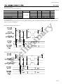
1
PEDL67Q5260-02
Issue Date: Jul, 2010
ML67Q5260
Preliminary
DFT Based Fingerprint Authentication LSI
GENERAL DESCRIPTION
The ML67Q5260 is a single chip LSI that executes fingerprint authentication without external memory by using the embedded
fingerprint authentication accelerator. This fingerprint authentication accelerator uses DFT(Discrete Fourier Transform) based
algorithm licensed from Precise Biometrics, and supports AuthenTec's slide sensors and certain touch sensors from several sensor
manufacturers. Besides the ML67Q5260 has the secure circuit to protect enrolled fingerprint data from unauthorized access. Thus
this LSI helps customers quickly design new products that offer convenient security as far as high performance fingerprint
authentication, low cost, small size and high level of security.
FEATURES
• Fingerprint authentication
- DFT (Discrete Fourier Transform) based algorithm licensed from Precise Biometrics
This DFT based algorithm achieves a lower FTE (False To Enrollment rate) and a higher authentication accuracy especially
when a slide sensor is used, as compared to the minutiae algorithm.
- Easy-to-use
The fingerprint authentication is performed by the fingerprint authentication accelerator, which does not ask customers
for so complicated control.
- No external memory
Customer’s application program and up to 45 fingerprint data can be stored in the embedded Flash memory on the ML67Q5260.
No external memory is required, when a slide sensor is used.
- High-speed authentication, besides low power consumption
The highly optimized fingerprint authentication accelerator achieves high-speed authentication using a low speed clock.
Authentication : < 0.8 seconds (1:1 authentication)
< 1.8 seconds (1:45 authentication)
Enrollment
: < 2 seconds/finger
- Applicable fingerprint sensor
Slide sensor
: AuthenTec AES1711 (128 × 8 pixels)
AuthenTec AES1751 (128 × 8 pixels)
• CPU
- 32-bit RISC CPU (ARM7TDMI-S)
- Little endian format
- Instruction system: A high-density 32-bit instruction and a 16-bit instruction of high-object efficiency, which is the subset of
the 32-bit instruction, can be executed in mixed mode.
- General-purpose register: 32 bits x 31 registers
- Built-in barrel shifter (ALU and barrel shift operation can be executed by one instruction)
- Built-in debugging function (JTAG interface)
The JTAG interface pin is shared with GPIO.
• Built-in Memories
- 16 Kbyte working RAM for CPU
- 128 Kbyte Flash ROM for application program and fingerprint template data, whose erase/rewrite times are maximum 10,000
- 8 Kbyte Mask ROM for update of program in the Built-in Flash ROM
• Interrupt control
- 1 FIQ resource
External : 1
- 20 IRQ resources
External : 3, Internal : 17
7 priority levels for each source
ARM is a registered trademark of ARM Limited. ARM7TDMI, ARM7TDMI-S, AMBA are a trademark of ARM Limited.
1/22
PEDL67Q5260-02
ML67Q5260
• DMA controller (DMAC)
- 2 channels
- Enable to allocate multiple DMA transfer request sources for each channel.
- Channel priority: fixed mode/round robin mode
- DMA transfer mode: cycle steal mode/burst mode
- DMA request type: software requests/hardware requests
- Maximum transfer count : 65,536
- Data transfer size: 8 bits/16 bits/32 bits
- Transfer request source: CPU, SPI, Synchronous SIO, Smartcard IF
• GPIO
- 13 bits × 1 channel, 12 bits × 1 channel
- Enable to setting input mode or output mode for each bit
- Enable to setting as interruption source for each bit
- Interruption mode: level/edge and positive logic/negative logic
• Timer
- 16-bit auto reload timer × 4 channel
• Watch dog timer (WDT)
- 16-bit timer
- 8.389 seconds max. (when CPU operating frequency is 32 MHz)
- Enables generation of interrupt or reset by setting
• SIO (UART)
- Full-duplex asynchronous mode
- Built-in baud rate generator
• SPI
- 2 channels of full-duplex serial peripheral interfaces
- Operating mode: master mode/slave mode
- Data transfer size: 8 bits (byte) / 16 bits (word)
- Built-in 16-byte/16-word FIFO on the transmission side and the reception side
- Supports DMA transfer (master/slave mode)
• Synchronous SIO (SSIO)
- clock synchronous serial port × 1 channel
- Data transfer size : 8 bits (byte)
- Selectable clock polarity
- Selectable LSB first or MSB first
- Operation mode: master mode/slave mode
- Supports DMAC transfer (in master mode only)
• Smart Card interface (Smartcard IF)
- ISO UART × 1 channel
- Built-in 16-byte FIFO
- Built-in parity error counter in receive mode and transmit mode at automatic retransmission
- Supports asynchronous protocol of T = 0 and T = 1 according to ISO7816 and EMV
- Built-in error detection code generation and error detection functions by hardware
- Supports DMA transfer
• USB2.0 full-speed device
- Compliant with Universal Serial Bus (USB) 2.0
- Full speed (12 Mbps) × 1 port.
- End points: 5 or 6
- Supports all data transfer types (control transfer, bulk transfer, interrupt transfer, isochronous transfer).
- Built-in SOP generation and CRC5/16 generation functions
- Access size to data transfer FIFOs: 8 bits/16 bits/32 bits
2/22
PEDL67Q5260-02
ML67Q5260
• Random number generator (RANDOM)
- Generates 8-bit random numbers
• Clock
- Input clock: 12 MHz (oscillator connected)
- System clock (CPU operating clock): 32 MHz
System clock is generated by PLL using 12MHz clock.
- Output clock: 6/12 MHz for fingerprint sensor
• Power management
- Power saving mode
•Individual module clock stop mode:
Clock operation/stop can be set for each functional block.
•HALT mode:
Only CPU clock is stopped.
•STOP mode:
All clocks are stopped, and start /stop of internal PLL and oscillator circuit are selectable.
• Package
- 63-pin WCSP Package (S-UFLGA63-4.03x4.01-0.50-W)
3/22
PEDL67Q5260-02
ML67Q5260
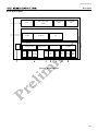
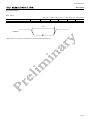
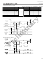
BLOCK DIAGRAM
Built-in ROM
8KB
Working RAM
16KB
Built-in Flash ROM
128 KB
CPU
AHB I/O
Interrupt
controller
Fingerprint
Accelerator
DMA controller
2ch
APB I/O
PLL
Clock/Reset/Power
Saving control
Timer
4ch
WDT
GPIO
2 ch
(25 bits)
Memory
Management
SIO
LSI controller
SPI
2ch
SSIO
1ch
Built-in FlashROM
controller
Smart
Card IF
1ch
USB
FS
Device
RAN
DOM
Figure 1 Block Diagram
4/22
PEDL67Q5260-02
ML67Q5260
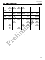
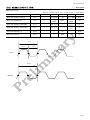
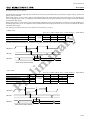
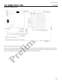
PIN LAYOUT
TESTF
PB01
(SIMVCTL0)
PB03
(SIMVCMD)
PB04
(SIMDATA)
PB06
(SIMCLK)
NTRST
VDDCORE
BSEL1
8
PA08
(SSIOTX)
PB00
(SIMDET)
VDDIO
VDDCORE
PR0
TDO
TCK
VDDIO
7
PA09
(SSIORX)
PA10
(SSIOCLK)
GNDIO
GNDCORE
GNDCORE
TDI
RTCK
GNDIO
6
AFSEL
PUCTL
PB02
(SIMVCTL1)
PB05
(SIMRST)
TMS
PA12
(SIORX)
GNDCORE
5
PB11
(CLKOUT)
GNDCORE
DP
PB08
(EXINT0)
XI
PA07
(SPI1SCK)
PA11
(SIOTX)
VDDCORE
4
VDDCORE
DM
PB09
(EXINT1)
RESETN
XO
PA00
(SPI0MOSI)
PA04
(SPI1MOSI)
PA02
(SPI0SSN)
3
VDDUSB
PB10
(VBUS)
VDDPLL
VDDIO
PA05
(SPI1MISO)
PA03
(SPI0SCK)
VDDIO
PA01
(SPI0MISO)
2
GNDUSB
PB07
(FIQ)
GNDPLL
PA06
(SPI1SSN)
TESTE
GNDIO
VDDCORE
GNDCORE
1
H
G
F
E
D
C
B
A
S-UFLGA61-4.03x4.01-0.50-W
(Bottom View)
5/22
PEDL67Q5260-02
ML67Q5260
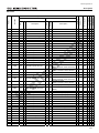
PIN LIST
PA05
I/O
-
General Purpose Port A5
B3
PA04
I/O
-
General Purpose Port A4
C2
A3
PA03
PA02
I/O
I/O
-
General Purpose Port A3
General Purpose Port A2
A2
PA01
I/O
-
General Purpose Port A1
C3
PA00
I/O
-
General Purpose Port A0
H4
PB11
I/O
-
General Purpose Port B11
G2
PB10
I/O
-
General Purpose Port B10
F3
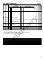
E4
G1
D8
D5
E8
F8
E5
G8
G7
G3
F4
G5
H8
A8
H5
D1
PB09
PB08
PB07
PB06
PB05
PB04
PB03
PB02
PB01
PB00
DM
DP
PUCTL
TESTF
BSEL1
AFSEL
TESTE
I/O
I/O
I/O
I/O
I/O
I/O
I/O
I/O
I/O
I/O
A
A
O
A
I
I
I
P
P
P
P
General Purpose Port B09
General Purpose Port B08
General Purpose Port B07
General Purpose Port B06
General Purpose Port B05
General Purpose Port B04
General Purpose Port B03
General Purpose Port B02
General Purpose Port B01
General Purpose Port B00
USB dev DUSB dev D+
USB dev Pull-up Control
FLASH Test Pin
Boot Device Select 1
JTAG Select (ARM/FLASH)
Test Mode Select
SIO Receive Data
SIO Transmit Data
SSIO Communication Clock
SSIO Receive Data
SSIO Transmit Data
SPI Clock for CH1
SPI Slave Select for CH1
SPI Data for CH1
I/O (Master Receive / Slave Transmit)
SPI Data for CH1
I/O (Master Transmit / Slave Receive)
I/O - SPI Clock for CH0
I N SPI Slave Select for CH0
SPI Data for CH0
I/O (Master Receive / Slave Transmit)
SPI Data for CH0
I/O (Master Transmit / Slave Receive )
O - Clock Output (for sensor)
External Interrupt Input ( for USB
I
VBUS)
I
- External Interrupt Input ( for IRQ 28)
I
- External Interrupt Input ( for IRQ 30)
I
- External Interrupt Input ( for FIQ)
O - Smartcard IF Clock
O N Smartcard IF Reset
I/O - Smartcard IF Serial Data
O - Smartcard IF Power Control
O - Smartcard IF Voltage Control 1
O - Smartcard IF Voltage Control 0
O - Smartcard IF Card Detection
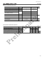
-
S
-
PU
PU
PU
PU
PU
PU
-
4mA
4mA
4mA
4mA
4mA
4mA
4mA
4mA
4mA
-
I O I I O L
I I I O H
I I I I I I I I -
-
-
4mA
-
I
-
-
-
4mA
-
I
-
-
-
4mA
4mA
-
I
I
-
-
-
4mA
-
I
-
-
-
4mA
-
I
-
-
-
4mA
-
I
-
S
-
4mA
T
I
-
4mA
4mA
4mA
4mA
4mA
4mA
4mA
4mA
4mA
4mA
4mA
-
-
I I I I I I I I I I I I O L
A I I I -
S S S - PD
- PD
- PD
Initial value
D2
I
O I/O I
O I/O I N
5V Tolerant
Oscillation Pin
Oscillation Pin
System Reset
Built-in ROM Port0 (*2)
JTAG Return Clock
JTAG Test Clock
JTAG Test Mode State
JTAG Test Data In
JTAG Test Data Out
JTAG Test Reset
General Purpose Port A12
General Purpose Port A11
General Purpose Port A10
General Purpose Port A9
General Purpose Port A8
General Purpose Port A7
General Purpose Port A6
Initial direction
N
P
P
N
-
Drive capacity
Polarity
I
I
O
I
I
I
O
I
I/O
I/O
I/O
I/O
I/O
I/O
I/O
Description
PU/PD(*1)
I/O
XI
XO
RESETN
PR0
RTCK
TCK
TMS
TDI
TDO
NTRST
PA12
PA11
PA10
PA09
PA08
PA07
PA06
Polarity
Pin name
D4
D3
E3
D7
B6
B7
C5
C6
C7
C8
B5
B4
G6
H6
H7
C4
E1
Description
Secondary function
I/O
Pin No.
Primary function
Schmitt
Description
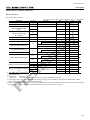
6/22
PEDL67Q5260-02
ML67Q5260
Polarity
Description
I/O
Polarity
Description
Schmitt
PU/PD(*1)
Drive capacity
5V Tolerant
Initial direction
Initial value
B8,
E7,
H3, VDDCORE
A4,
B1
E6,
D6,
A5, GNDCORE
G4,
A1
A7,
F7,
VDDIO
B2,
E2
A6,
F6,
GNDIO
C1
F2
VDDPLL
F1
GNDPLL
H2 VDDUSB
H1 GNDUSB
I/O
Pin name
Pin No.
Description
-
-
1.8V Power Supply for CORE
-
-
-
-
-
-
-
-
-
-
-
Ground for CORE
-
-
-
-
-
-
-
-
-
-
-
3.3V Power Supply for IO
-
-
-
-
-
-
-
-
-
-
-
Ground for IO
-
-
-
-
-
-
-
-
-
-
-
1.8V Power Supply for PLL
Ground for PLL
3.3V Power Supply for USB
Ground for PLL
-
-
-
-
-
-
-
-
-
Primary function
Secondary function
*1: PU/PD column:
PU: Pulled up with a built-in resistor
PD: Pulled down with a built-in resistor
*2: This pin is used in the Built-in ROM for an update function of the Built-in FlashROM.
For details, see the User's manual for USB firmware update function.
Termination of Pins Not Used
Pin name
Pin termination
DM, DP, PUCTL
Open
PA00-12 PB00-11
TDO, RTCK
TCK, TMS, TDI, NTRST
TESTF
Pulled down
Open
Pulled up
Must be used as open
7/22
PEDL67Q5260-02
ML67Q5260
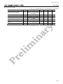
ABSOLUTE MAXIMUM RATINGS
Parameter
Digital power supply voltage CORE (1.8 V)
PLL power supply voltage (1.8 V)
Digital power supply voltage I/O (3.3 V)
USB power supply voltage I/O (3.3 V)
Symbol
VDD_CORE
VDD_PLL
VDD_IO
VDD_USB
Condition
Rating
—
−0.3 to +2.5
—
−0.3 to +4.6
—
−0.3 to VDD_IO+0.3
VI
VDD_IO = 3.0 V to 3.6 V
VDD_IO < 3.0 V
−0.3 to +6.0
−0.3 to VDD_IO+0.3
VO
—
−0.3 to VDD_IO+0.3
II
—
−10 to +10
“H” output allowable current
IOH
—
+10
“L” output allowable current
IOL
—
−10
Power dissipation
PD
Ta = 85°C
600
mW
TSTG
—
−50 to 150
°C
Input voltage (normal buffer)
Input voltage (5 V tolerant)
Output voltage
Input allowable current
Storage temperature
Unit
V
mA
GUARANTEED OPERATING RANGES
Parameter
Digital power supply voltage (CORE) (*1)
PLL power supply voltage (*1)
Digital power supply voltage (I/O)
USB power supply voltage
Ambient temperature
Flash write count
Symbol
VDD_CORE
VDD_PLL
VDD_IO
VDD_USB
Ta
(GND = 0 V)
Unit
Condition
Min.
Typ.
Max.
—
1.62
1.62
3.0
3.0
–40
1.8
1.8
3.3
3.3
25
1.98
1.98
3.6
3.6
85
°C
—
—
10,000
cycle
CWR
V
* 1: Please supply from same power source to both VDD_CORE pins and VDD_PLL pin.
8/22
PEDL67Q5260-02
ML67Q5260
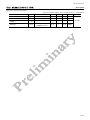
ELECTRICAL CHARACTERISTICS
DC Characteristics
DC characteristics (Core/IO)
Parameter
Symbol
“H” input voltage
“L” input voltage
Schmitt trigger
input threshold voltage
(3.3 V)
Schmitt trigger
input threshold voltage
(5 V tolerant)
VIH
VIL
(VDD_CORE = 1.62 to 1.98 V, VDD_IO = 3.0 to 3.6 V, Ta = −40 to +85°C)
Condition
Min.
Typ.
Max.
Unit
2.0
−0.3
—
—
VDD_IO +0.3
0.8
—
—
2.0
VT-
0.6
—
—
VT+
—
—
2.0
0.6
—
—
—
—
VT+
—
—
VT-
“H” output voltage
VOH
IOH = −4 mA
2.4
—
—
“L” output voltage
VOL
IOL = 4 mA
VIH = VDD_IO
pull-down
VIH = VDD_IO
VIH = 5.5 V
VIL = 0 V
—
—
10
—
—
−10
—
—
62
—
—
—
0.4
10
120
10
30
—
−140
−78
−20
−10
—
—
High level input current (*1)
IIH
High level input current (*2)
Low level input current (*1)
IIL
Low level input current (*2)
pull-up
VIL = 0 V
IOZH
3-state output leakage current
IOZL
IDDS1_CORE
IDDS1_IO
IDDS1_PLL
IDDO_CORE
Supply current (during operation)
IDDO_IO
(*5)
IDDO_PLL
Supply current (during STOP) (*4)
V
VOH = VDD_IO
pull-down
VOL = 0 V
pull-up
—
(*3)
—
fBUSCLK = 32.0 MHz , no load
—
—
10
10
62
120
−10
−140
—
—
—
—
—
—
—
−78
80
4
2
50
5
1
—
−20
1500
20
10
70
10
3
μA
μA
μA
mA
*1: Pins other than 5 V tolerant pins
*2: 5 V tolerant pins
*3: Input ports:
VDD_IO or 0 V
Other ports:
No load excluding the current flowing in pull-up/pull-down resistors
*4: LSI supply current when going into LSI stop mode by stopping clock oscillation, PLL operation, and random number
generator operation and setting USB power-down mode.
*5: The current supplied to the LSI when fingerprint authentication is executed without USB operation under the conditions that
the programs are stored in the built-in Flash ROM and no external memory are connected.
9/22
PEDL67Q5260-02
ML67Q5260
DC characteristics (USB)
Parameter
Symbol
(VDD_CORE = 1.62 to 1.98V, VDD_IO = 3.0 to 3.6V, Ta = −40 to +85°C)
Condition
Min.
Typ.
Max.
Unit
Absolute value of the
difference between the DP
and DM pins
Includes VDI range
Differential input sensitivity
VDI
0.2
—
—
V
Differential common mode range
Single end input threshold voltage
VCM
VSE
0.8
0.8
—
—
2.5
2.0
V
V
High level output voltage
VOH
Low level output voltage
Hi-Z state input/output leakage
current
Driver output resistance
VOL
15K W RL is connected
to GND
1.5K W RL to 3.6 V
2.8
—
—
V
—
—
0.3
V
ILO
0 V < VIN < 3.3 V
–10
—
10
μA
ZDRV
Steady state
28
—
44
Ω
10/22
PEDL67Q5260-02
ML67Q5260
AC Characteristics
Reset Timing
Parameter
Reset pulse width
Symbol
tRSTW
(VDD_CORE = 1.62 to 1.98 V, VDD_IO = 3.0 to 3.6 V, Ta = −40 to +85°C)
Condition
Min.
Typ.
Max.
Unit
—
6.0
—
—
ms
tRSTW
RESETN
*When power on, release the reset after the clock oscillation stabilization.
11/22
PEDL67Q5260-02
ML67Q5260
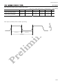
Main Clock Timing
Parameter
Symbol
(VDD_CORE = 1.62 to 1.98 V, VDD_IO = 3.0 to 3.6 V, Ta = −40 to +85°C)
Condition
Min.
Typ.
Max.
Unit
Main clock (XI/XO) frequency
fSYSC
—
12 × 0.9975
12
12 × 1.0025
Main clock (XI/XO) cycle
tSYSC
—
83.33 ×
0.9975
83.33
Main clock (XI/XO) H pulse width
tSYSCH
—
0.45 × tSYSC
—
Main clock (XI/XO) L pulse width
tSYSCL
—
0.45 × tSYSC
—
Bus clock frequency (*1)
fBUSCLK
—
—
32
—
MHz
Bus clock cycle (*1)
tBUSCLK
—
—
31.25
—
ns
83.33 ×
1.0025
0.55 ×
tSYSC
0.55 ×
tSYSC
MHz
ns
ns
ns
* 1: Main system bus clock within the LSI and operating clocks of CPU, DMA, etc.
tSYSC
tSYSCH
tSYSCL
XI/XO
tBUSCLK
BUSCLK
12/22
PEDL67Q5260-02
ML67Q5260
USB Access Timing (Full-Speed)
(VDD_CORE = 1.62 to 1.98 V, VDD_IO = 3.0 to 3.6 V, Ta = −40 to +85°C)
Parameter
Rise time
Fall time
Output signal crossover
voltage
Data rate
Symbol
Condition
Min.
Typ.
Max.
Unit
TR
TF
CL = 50 pF
CL = 50 pF
4
4
—
—
20
20
ns
ns
VCRS
CL = 50 pF
0.8
—
2.5
V
TDRATE
Average bit rate
(12Mbps ±0.25%)
11.97
—
12.03
Mbps
Applied pin
DP, DM
13/22
PEDL67Q5260-02
ML67Q5260
SPI Access Timing
- Characteristics of master mode timing
Parameter
Data delay time (output)
Data setup time (input)
Data hold time (input)
SSN-SCK lead time
SCK-SSN lag time
Symbol
tDD
tSD
tHD
tLEAD
tLAG
Condition
CL = 30 pF
(VDD_CORE = 1.62 to 1.98 V, VDD_IO = 3.0 to 3.6 V, Ta = −40 to +85°C)
Min.
Typ.
Max.
Unit
—
—
25
ns
25
—
—
ns
0 (*1)
—
—
ns
0.5*tSCK −15
—
0.5*tSCK +15
ns(*2)
0.5*tSCK −15
—
0.5*tSCK +15
ns(*2)
* 1: Although actual values may become negative depending on the external load, input the serial data so that the data hold time
can be guaranteed.
* 2: tSCK is the cycle time of the serial clock for SPI transferring which is obtained by dividing the frequency of the bus clock,
whose cycle time is tBUSCLK.
SPI master mode timing (CPHA = 0)
SPI master mode timing (CPHA = 1)
14/22
PEDL67Q5260-02
ML67Q5260
- Characteristics of slave mode timing
Parameter
(VDD_CORE = 1.62 to 1.98 V, VDD_IO = 3.0 to 3.6 V, Ta = −40 to +85°C)
Condition
Min.
Typ.
Max.
Unit
Symbol
Serial clock cycle time
Serial clock High/Low time
Data delay time (output)
Data setup time (input)
Data hold time (input)
SSN-SCK lead time
SCK-SSN lag time
Slave data invalid time
SPI bus I/O rise/fall time
tSCK
T.B.D
—
—
tBUSCLK
tWSCK
T.B.D
—
—
tBUSCLK
tDD
tSD
tHD
—
25
25
25
—
—
—
—
—
—
—
25
—
—
—
—
25
T.B.D
ns
ns
ns
ns
ns
ns
ns
CL = 30 pF
tLEAD
tLAG
tDIS
tr, tf
tBUSCLK + 15
—
—
SPI slave mode timing (CPHA = 0)
SPInSSN
(Input)
tSCK
tLEAD
tLAG
SPInSCK
(CPOL=0, Input)
tWSCK
SPInSCK
(CPOL=1, Input)
tDIS
tDD
SPInMISO
(Output)
LSB
tSD
SPInMOSI
(Input)
tWSCK
MSB
tHD
LSB
MSB
*n:0,1
SPI slave mode timing (CPHA = 1)
15/22
PEDL67Q5260-02
ML67Q5260
Synchronous SIO Access Timing
Switching between master mode and slave mode can be set for this synchronous SIO by the software register setting. Serial clock
polarity can be switched.
When clock polarity is set to positive, data is transmitted (shifted out) on the falling edge of the clock and is received (shifted in)
on the rising edge of the clock. At completion of 8-bit data transmission/reception, the clock stops at a high level and the last data
is retained for data output.
When clock polarity is set to negative, data is transmitted (shifted out) on the rising edge of the clock and is received (shifted in) on
the falling edge of the clock. At completion of 8-bit data transmission/reception, the clock stops at a low level and the last data is
retained for data output.
The following waveforms show the cases where the clock polarity is positive.
− Master mode
Parameter
Output data delay time
Input data setting time
Input data retained time
Symbol Condition
tMSSOD
tMSSIS CL = 30 pF
tMSSIH
(VDD_CORE = 1.62 to 1.98 V, VDD_IO = 3.0 to 3.6 V, Ta = −40 to +85°C)
Min.
Typ.
Max.
Unit
—
—
20
ns
30
—
—
10
—
—
Note:
11 clock outputs for transferring is selectable from 2 synchronous SIO clock sources and the frequency divide ratios.
SSIOCLK *
t MSSOD
SSIOTX
t MSSIS
t MSSIH
SSIORX
* Serial clock: Positive polarity
− Slave mode
Parameter
Serial clock cycle
Output data delay time
Input data setting time
Input data retained time
Symbol Condition
T
tSSSOD
CL = 30 pF
tSSSIS
tSSSIH
(VDD_CORE = 1.62 to 1.98 V, VDD_IO = 3.0 to 3.6 V, Ta = −40 to +85°C)
Min.
Typ.
Max.
Unit
62.5
—
—
—
—
40
ns
20
—
—
20
—
—
T
SSIOCLK *
t SSSOD
SSIOTX
t SSSIS
t SSSIH
SSIORX
* Serial clock: Positive polarity
16/22
PEDL67Q5260-02
ML67Q5260
GPIO (PA, PB) Access Timing
Parameter
(VDD_CORE = 1.62 to 1.98 V, VDD_IO = 3.0 to 3.6 V, Ta = −40 to +85°C)
Condition
Min.
Typ.
Max.
Unit
Symbol
PAn, PBm input H duration
PAn, PBm input L duration
TGPIOIH
TGPIOIL
—
—
tBUSCLK ×2
tBUSCLK ×2
—
—
—
—
ns
ns
Note 1: n = 12 to 0, m=11 to 0
{ PAn, PBm input timing (n = 12 to 0, m = 11 to 0)
TG PIO IH
TG PI OI L
PAn/
PBm/
17/22
PEDL67Q5260-02
ML67Q5260
Clock Output (Secondary Function of PB11 Pin) Timing
Parameter
Symbol
(VDD_CORE = 1.62 to 1.98 V, VDD_IO = 3.0 to 3.6 V, Ta = −40 to +85°C)
Condition
Min.
Typ.
Max.
Unit
Clock output High duration
tCLKOUT_H
—
Clock output Low duration
tCLKOUT_L
—
45% ×
tCLKOUT
45% ×
tCLKOUT
50% ×
tCLKOUT
50% ×
tCLKOUT
55% ×
tCLKOUT
55% ×
tCLKOUT
ns(*1)
ns(*1)
*tCLKOUT is the cycle time of the 6 MHz or 12 MHz clock generated by 2 clock sources and the frequency divide ratio.
Clock output (secondary function of PB11 pin) timing
tCLKOUT_H
tCLKOUT_L
tCLKOUT
18/22
PEDL67Q5260-02
ML67Q5260
POWER ON / OFF SEQUENCE
Power ON sequence
- Core and IO power should be on at the same time, or IO power should be on after Core on.
Power ON Sequence
3.3 V
VDDIO
VDDCORE, VDDPLL
1.8 V
0V
Power OFF sequence
- Core and IO power should be off at the same time, or Core power should be off after IO off.
Power OFF Sequence
3.3 V
1.8 V
VDDIO
VDDCORE, VDDPLL
0V
19/22
PEDL67Q5260-02
ML67Q5260
PACKAGE DIMENSIONS
4.05
(0.285)
4.07
(0.275)
(Unit: mm)
Notes for Mounting the Surface Mount Type Package
The surface mount type packages are very susceptible to heat in reflow mounting and humidity absorbed in storage. Therefore,
before you perform reflow mounting, contact Oki’s responsible sales person for the product name, package name, pin number,
package code and desired mounting conditions (reflow method, temperature and times).
20/22
PEDL67Q5260-02
ML67Q5260
REVISION HISTORY
Document No.
Date
PEDL67Q5260-01
PEDL67Q5260-02
Aug.18, 2009
Jul.15, 2010
Page
Previous
Current
Edition
Edition
–
–
–
–
Description
Preliminary edition 1
Preliminary edition 2
21/22
PEDL67Q5260-02
ML67Q5260
NOTICE
1. The information contained herein can change without notice owing to product and/or technical improvements. Before using the
product, please make sure that the information being referred to is up-to-date.
2. The outline of action and examples for application circuits described herein have been chosen as an explanation for the standard
action and performance of the product. When planning to use the product, please ensure that the external conditions are
reflected in the actual circuit, assembly, and program designs.
3. When designing your product, please use our product below the specified maximum ratings and within the specified operating
ranges including, but not limited to, operating voltage, power dissipation, and operating temperature.
4. OKI Semiconductor assumes no responsibility or liability whatsoever for any failure or unusual or unexpected operation
resulting from misuse, neglect, improper installation, repair, alteration or accident, improper handling, or unusual physical or
electrical stress including, but not limited to, exposure to parameters beyond the specified maximum ratings or operation
outside the specified operating range.
5. Neither indemnity against nor license of a third party’s industrial and intellectual property right, etc. is granted by us in
connection with the use of the product and/or the information and drawings contained herein. No responsibility is assumed by
us for any infringement of a third party’s right which may result from the use thereof.
6. The products listed in this document are intended for use in general electronics equipment for commercial applications (e.g.,
office automation, communication equipment, measurement equipment, consumer electronics, etc.). These products are not,
unless specifically authorized by OKI Semiconductor, authorized for use in any system or application that requires special or
enhanced quality and reliability characteristics nor in any system or application where the failure of such system or application
may result in the loss or damage of property, or death or injury to humans.
Such applications include, but are not limited to, traffic and automotive equipment, safety devices, aerospace equipment,
nuclear power control, medical equipment, and life-support systems.
7. Certain products in this document may need government approval before they can be exported to particular countries. The
purchaser assumes the responsibility of determining the legality of export of these products and will take appropriate and
necessary steps at their own expense for these.
8. No part of the contents contained herein may be reprinted or reproduced without our prior permission.
Copyright 2009 - 2010 Oki Semiconductor Co., Ltd.
22/22