1
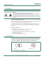
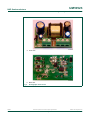
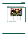
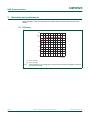
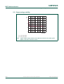
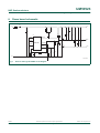
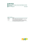
UM10523 TEA1721 universal mains white goods flyback SMPS demo board Rev. 1 — 27 January 2012 User manual Document information Info Content Keywords TEA1721XT, flyback, non-isolated, dual output, white goods, SMPS, very low no-load power, primary-side feedback Abstract This user manual describes the TEA1721 based 12 V and 3.3 V AC/DC SMPS demo board which provides 5 W into a load. UM10523 NXP Semiconductors Universal mains white goods flyback SMPS demo board Revision history Rev Date Description v.1 20120127 first issue Contact information For more information, please visit: http://www.nxp.com For sales office addresses, please send an email to: [email protected] UM10523 User manual All information provided in this document is subject to legal disclaimers. Rev. 1 — 27 January 2012 © NXP B.V. 2012. All rights reserved. 2 of 14 UM10523 NXP Semiconductors Universal mains white goods flyback SMPS demo board 1. Introduction WARNING Lethal voltage and fire ignition hazard The non-insulated high voltages that are present when operating this product, constitute a risk of electric shock, personal injury, death and/or ignition of fire. This product is intended for evaluation purposes only. It shall be operated in a designated test area by personnel qualified according to local requirements and labor laws to work with non-insulated mains voltages and high-voltage circuits. This product shall never be operated unattended. This user manual describes the TEA1721 based 12 V and 3.3 V AC/DC SMPS demo board which provides 5 W into a load. The switch-mode converter operates in flyback mode at a maximum frequency of around 50 kHz. Over-current and short circuit protection are built in. Under no-load conditions, the power consumption of the flyback converter is around 20 mW. This application is typically suited for White Goods appliances and industrial applications. 1.1 Features and benefits • • • • • Compatible with Universal Mains 85 V (AC) to 265 V (AC) Dual output voltage 12 V (DC) and 3.3 V (DC) Primary side voltage regulation removes the need for an optocoupler Total maximum power is 5 W No-load power consumption of 20 mW 2. Safety Warning The demo board is powered by AC mains voltage. Avoid touching the board when power is applied. An isolated housing is obligatory when used in uncontrolled, non-laboratory environments. Always provide galvanic isolation of the mains phase using a variable transformer. The following symbols identify isolated and non-isolated devices. 019aab174 019aab173 a. Isolated Fig 1. UM10523 User manual b. Non-isolated Isolated and non-isolated symbols All information provided in this document is subject to legal disclaimers. Rev. 1 — 27 January 2012 © NXP B.V. 2012. All rights reserved. 3 of 14 UM10523 NXP Semiconductors Universal mains white goods flyback SMPS demo board 3. Specification Table 1. Demo board specification Parameter Value Comment AC line input voltage 85 V (AC) to 265 V (AC) supplied to J1 (Live) and J2 (Neutral) terminals Output voltage 12 V (DC) and 3.3 V (DC) with supplied from connectors: respect to neutral J2.1 = 0 V, GND[1][2] J2.2 = 3.3 V J2.3 = 12 V Maximum output current Maximum output power 12 V = 400 mA 3.3 V = 400 mA - 5W - requires a concurrent minimum load on the 12 V output of approximately 50 mA Output voltage accuracy 12 V = +5 % to 5 % adjustable using resistor R3. Output voltage regulation and stability 12 V = 1 % in load range 5 % to 100 %[3] Maximum output ripple current 100 mV peak to peak under full load on the 12 V (DC) output No-load power consumption 20 mW - Efficiency 80 % - Operating temperature 40 C to 85 C - EMC filtering not applicable It is assumed that EMI filtering is performed using an external Mains filter in the (white goods) appliance. If compliance with regulations is required for the standalone SMPS, the appropriate filtering stage(s) must be separately implemented. Board dimensions 34.3 mm 34.3 mm 21 mm LBH [1] J2.1 is at the same potential as J1.2. [2] The output voltage can be adjusted with resistor R3. The turns ratio of the secondary windings on transformer T1 defines the ratio between the two output voltages. [3] Output voltage regulation can deviate by up to +8 % under the no load condition. The variation can be reduced by changing the Zener voltage of the D7 and/or D8 Zener diodes. Reducing the D7 and D8 Zener diode voltage can have marginal consequences for the no-load power consumption. UM10523 User manual All information provided in this document is subject to legal disclaimers. Rev. 1 — 27 January 2012 © NXP B.V. 2012. All rights reserved. 4 of 14 UM10523 NXP Semiconductors Universal mains white goods flyback SMPS demo board a. Front view. b. Back view. Fig 2. UM10523 User manual Photographs of the board All information provided in this document is subject to legal disclaimers. Rev. 1 — 27 January 2012 © NXP B.V. 2012. All rights reserved. 5 of 14 UM10523 NXP Semiconductors Universal mains white goods flyback SMPS demo board 4. Demo board connections Remark: Mount the board in a shielded or isolated box for demonstration purposes. Fig 3. UM10523 User manual TEA1721XT Demo board connections All information provided in this document is subject to legal disclaimers. Rev. 1 — 27 January 2012 © NXP B.V. 2012. All rights reserved. 6 of 14 UM10523 NXP Semiconductors Universal mains white goods flyback SMPS demo board 5. Operation and performance Basic operation of the IC is described in the NXP Semiconductors TEA1721XT data sheets. 5.1 Efficiency aaa-002239 100 η (%) (1) (2) 80 60 40 20 0 0 1000 2000 3000 4000 5000 Pout (mW) (1) 115 V (AC) input. (2) 230 V (AC) input. Fig 4. UM10523 User manual Typical efficiency of the TEA1721 universal mains white goods flyback controller as a function of load All information provided in this document is subject to legal disclaimers. Rev. 1 — 27 January 2012 © NXP B.V. 2012. All rights reserved. 7 of 14 UM10523 NXP Semiconductors Universal mains white goods flyback SMPS demo board 5.2 Output voltage stability aaa-002240 -14 Vout (V) -13 -12 (1) (2) -11 -10 0 1000 2000 3000 4000 5000 Pout (mW) (1) 115 V (AC) input. (2) 230 V (AC) input. Fig 5. UM10523 User manual Typical output voltage stability of the TEA1721 universal mains white goods flyback controllers a function of load All information provided in this document is subject to legal disclaimers. Rev. 1 — 27 January 2012 © NXP B.V. 2012. All rights reserved. 8 of 14 UM10523 NXP Semiconductors Universal mains white goods flyback SMPS demo board 6. Demo board schematic J1.1 R1 D1 J2.1 R3 C3 D7 C1 R4 T1 C6 IC1 GND1 C8 D3 DRAIN D5 J2.2 GND2 GND3 TEA1721 D4 VCC FB R6 R2 C2 C4 C9 C7 R7 SOURCE D6 D8 J2.3 C5 R5 J1.2 aaa-002241 Fig 6. TEA1721 white goods SMPS circuit diagram UM10523 User manual All information provided in this document is subject to legal disclaimers. Rev. 1 — 27 January 2012 © NXP B.V. 2012. All rights reserved. 9 of 14 UM10523 NXP Semiconductors Universal mains white goods flyback SMPS demo board 7. PCB components Table 2. Demo board components Reference Description and value Part number Manufacturer C1 electrolytic capacitor; 2E pitch; 4.7 F; 400 V - - C2 capacitor; 10 pF; 400 V; 0805 - - C3 capacitor; 220 pF; 500 V; 0805 - - C4 capacitor; 1 F; 50 V; 0805 - - C5 electrolytic capacitor; 1E pitch; 10 F; 35 V - - C6 electrolytic capacitor; 1E pitch; 470 F; 10 V - - C7 electrolytic capacitor; 1E pitch; 470 F; 16 V - - C8 capacitor; 100 nF; 25 V; 0805 - - C9 capacitor; 100 nF; 25 V; 0805 - - D1 diode; S1M; SMA - Fairchild D2 not mounted; diode; BZG03-C200; SMA BZG03-C200 - D3 diode; S1M; SMA - Fairchild D4 diode; BAS316; SOD323 - NXP Semiconductors D5 diode; BYG20J; SMA BYG20J - D6 diode; PMEG4050EP; SOD128 - - D7 diode; BZX384-C3V6; SOD323 BZX384-C3V6 NXP Semiconductors D8 diode; BZX384-C13; SOD323 BZX384-C13 NXP Semiconductors IC1 TEA1721; SO7 - NXP Semiconductors J1.1, J1.2 2-pole terminal block; 2E pitch 1729128 Phoenix J2.1; J2.2; J2.3 3-pole terminal block; 2E pitch 1729131 Phoenix T1 Würth Elektronik 750311993; EE16[1] - Würth Elektronik R1 carbon resistor; 22 ; 4E pitch - R2 resistor; 4.7 k; 1 %; 0805 - R3 resistor; 100 k; 0.5 W; 1206 - R4 resistor; 470 ; 0805 - R5 resistor; 1.8 ; 0.25 W; 1206 - %[2] R6 resistor; 18 k; 1 R7 resistor; 10 ; 0805 - [1] Custom-made transformer. Primary winding inductance: 2.4 mH, turns ratio primary : secondary : auxiliary = 6.5 : 1 : 1. The secondary winding must have a tap for the 3.3 V output voltage. [2] To tune the output voltage, change this value. UM10523 User manual All information provided in this document is subject to legal disclaimers. Rev. 1 — 27 January 2012 © NXP B.V. 2012. All rights reserved. 10 of 14 UM10523 NXP Semiconductors Universal mains white goods flyback SMPS demo board 8. Implementation guidelines • The maximum current allowed in for the TEA1721 internal switching MOSFET is 700 mA. When adapting this circuit, take care to ensure that this current value is not exceeded under any circumstances. • Resistor R1 limits the inrush current. The resistor must be a carbon resistor because metal film resistors can act as a fuse in this position. If no current limiting is required, the resistor can be replaced with a short-circuit. • Zener diodes D7 and D8 form a small pre-load and act as overvoltage spike suppressors. If no over-voltage suppression is necessary, the Zener diodes can be replaced with small resistors. • Capacitors C7 and C8 are mounted for additional HF noise suppression. If it is not needed, these components can be omitted. UM10523 User manual All information provided in this document is subject to legal disclaimers. Rev. 1 — 27 January 2012 © NXP B.V. 2012. All rights reserved. 11 of 14 UM10523 NXP Semiconductors Universal mains white goods flyback SMPS demo board 9. Board layout a. Top silk screen plus top component placement and drill pattern b. Bottom copper and bottom silk screen plus component placement Fig 7. PCB layout The bottom silk screen is normally not used in PCB production. Merged with the bottom copper, it is shown here as a component placement reference only. See Table 3 for a list of components. Table 3. Drill tool table Drill tool code Drill diameter C 1 mm D 0.9 mm E 1.3 mm 10. References UM10523 User manual [1] TEA1721XT - Ultra-low standby SMPS controller with integrated power switch [2] AN11060 - TEA172X 5 W to 11 W power supply/USB charger All information provided in this document is subject to legal disclaimers. Rev. 1 — 27 January 2012 © NXP B.V. 2012. All rights reserved. 12 of 14 UM10523 NXP Semiconductors Universal mains white goods flyback SMPS demo board 11. Legal information 11.1 Definitions Draft — The document is a draft version only. The content is still under internal review and subject to formal approval, which may result in modifications or additions. NXP Semiconductors does not give any representations or warranties as to the accuracy or completeness of information included herein and shall have no liability for the consequences of use of such information. 11.2 Disclaimers Limited warranty and liability — Information in this document is believed to be accurate and reliable. However, NXP Semiconductors does not give any representations or warranties, expressed or implied, as to the accuracy or completeness of such information and shall have no liability for the consequences of use of such information. NXP Semiconductors takes no responsibility for the content in this document if provided by an information source outside of NXP Semiconductors. In no event shall NXP Semiconductors be liable for any indirect, incidental, punitive, special or consequential damages (including - without limitation - lost profits, lost savings, business interruption, costs related to the removal or replacement of any products or rework charges) whether or not such damages are based on tort (including negligence), warranty, breach of contract or any other legal theory. Notwithstanding any damages that customer might incur for any reason whatsoever, NXP Semiconductors’ aggregate and cumulative liability towards customer for the products described herein shall be limited in accordance with the Terms and conditions of commercial sale of NXP Semiconductors. Right to make changes — NXP Semiconductors reserves the right to make changes to information published in this document, including without limitation specifications and product descriptions, at any time and without notice. This document supersedes and replaces all information supplied prior to the publication hereof. Suitability for use — NXP Semiconductors products are not designed, authorized or warranted to be suitable for use in life support, life-critical or safety-critical systems or equipment, nor in applications where failure or malfunction of an NXP Semiconductors product can reasonably be expected to result in personal injury, death or severe property or environmental damage. NXP Semiconductors and its suppliers accept no liability for inclusion and/or use of NXP Semiconductors products in such equipment or applications and therefore such inclusion and/or use is at the customer’s own risk. Applications — Applications that are described herein for any of these products are for illustrative purposes only. NXP Semiconductors makes no representation or warranty that such applications will be suitable for the specified use without further testing or modification. UM10523 User manual Customers are responsible for the design and operation of their applications and products using NXP Semiconductors products, and NXP Semiconductors accepts no liability for any assistance with applications or customer product design. It is customer’s sole responsibility to determine whether the NXP Semiconductors product is suitable and fit for the customer’s applications and products planned, as well as for the planned application and use of customer’s third party customer(s). Customers should provide appropriate design and operating safeguards to minimize the risks associated with their applications and products. NXP Semiconductors does not accept any liability related to any default, damage, costs or problem which is based on any weakness or default in the customer’s applications or products, or the application or use by customer’s third party customer(s). Customer is responsible for doing all necessary testing for the customer’s applications and products using NXP Semiconductors products in order to avoid a default of the applications and the products or of the application or use by customer’s third party customer(s). NXP does not accept any liability in this respect. Export control — This document as well as the item(s) described herein may be subject to export control regulations. Export might require a prior authorization from competent authorities. Evaluation products — This product is provided on an “as is” and “with all faults” basis for evaluation purposes only. NXP Semiconductors, its affiliates and their suppliers expressly disclaim all warranties, whether express, implied or statutory, including but not limited to the implied warranties of non-infringement, merchantability and fitness for a particular purpose. The entire risk as to the quality, or arising out of the use or performance, of this product remains with customer. In no event shall NXP Semiconductors, its affiliates or their suppliers be liable to customer for any special, indirect, consequential, punitive or incidental damages (including without limitation damages for loss of business, business interruption, loss of use, loss of data or information, and the like) arising out the use of or inability to use the product, whether or not based on tort (including negligence), strict liability, breach of contract, breach of warranty or any other theory, even if advised of the possibility of such damages. Notwithstanding any damages that customer might incur for any reason whatsoever (including without limitation, all damages referenced above and all direct or general damages), the entire liability of NXP Semiconductors, its affiliates and their suppliers and customer’s exclusive remedy for all of the foregoing shall be limited to actual damages incurred by customer based on reasonable reliance up to the greater of the amount actually paid by customer for the product or five dollars (US$5.00). The foregoing limitations, exclusions and disclaimers shall apply to the maximum extent permitted by applicable law, even if any remedy fails of its essential purpose. 11.3 Trademarks Notice: All referenced brands, product names, service names and trademarks are the property of their respective owners. All information provided in this document is subject to legal disclaimers. Rev. 1 — 27 January 2012 © NXP B.V. 2012. All rights reserved. 13 of 14 UM10523 NXP Semiconductors Universal mains white goods flyback SMPS demo board 12. Contents 1 1.1 2 3 4 5 5.1 5.2 6 7 8 9 10 11 11.1 11.2 11.3 12 Introduction . . . . . . . . . . . . . . . . . . . . . . . . . . . . 3 Features and benefits . . . . . . . . . . . . . . . . . . . . 3 Safety Warning. . . . . . . . . . . . . . . . . . . . . . . . . . 3 Specification. . . . . . . . . . . . . . . . . . . . . . . . . . . . 4 Demo board connections . . . . . . . . . . . . . . . . . 6 Operation and performance . . . . . . . . . . . . . . . 7 Efficiency . . . . . . . . . . . . . . . . . . . . . . . . . . . . . 7 Output voltage stability . . . . . . . . . . . . . . . . . . . 8 Demo board schematic . . . . . . . . . . . . . . . . . . . 9 PCB components . . . . . . . . . . . . . . . . . . . . . . . 10 Implementation guidelines . . . . . . . . . . . . . . . 11 Board layout . . . . . . . . . . . . . . . . . . . . . . . . . . . 12 References . . . . . . . . . . . . . . . . . . . . . . . . . . . . 12 Legal information. . . . . . . . . . . . . . . . . . . . . . . 13 Definitions . . . . . . . . . . . . . . . . . . . . . . . . . . . . 13 Disclaimers . . . . . . . . . . . . . . . . . . . . . . . . . . . 13 Trademarks. . . . . . . . . . . . . . . . . . . . . . . . . . . 13 Contents . . . . . . . . . . . . . . . . . . . . . . . . . . . . . . 14 Please be aware that important notices concerning this document and the product(s) described herein, have been included in section ‘Legal information’. © NXP B.V. 2012. All rights reserved. For more information, please visit: http://www.nxp.com For sales office addresses, please send an email to: [email protected] Date of release: 27 January 2012 Document identifier: UM10523