1
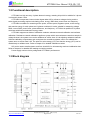
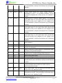
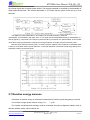
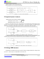
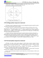
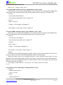
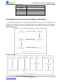
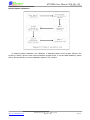
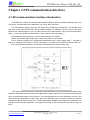
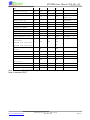
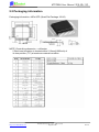
ATT7026A User Manual(210-SD-112)
ATT7026A
User Manual
版权归钜泉光电科技(上海)有限公司所有
http://www.hitrendtech.com
Page1 of 40
Rev1.0
ATT7026A User Manual(210-SD-112)
Table of Contents
Chapter 1 Introduction ············································································································································3
1.1 Features·····················································································································································3
1.2 Functional description ·······························································································································4
1.3 Block diagram···········································································································································4
1.4 Pin definition·············································································································································5
1.5 Application diagram··································································································································8
Chapter 2 System Functions····································································································································9
2.1 Power supply monitor ·······························································································································9
2.2 System reset ··············································································································································9
2.3 ADC························································································································································ 10
2.4 Active power measure ····························································································································· 11
2.5 Active energy measure ···························································································································· 11
2.6 Reactive power measure·························································································································· 11
2.7 Reactive energy measure························································································································· 12
2.8 apparent power measure·························································································································· 13
2.9 Voltage RMS measure ···························································································································· 13
2.10 Current RMS measure ··························································································································· 14
2.11 Voltage line-frequency measure ············································································································ 14
2.12 Power factor measure ···························································································································· 14
2.13 Voltage and current phase angle measure ······························································································ 14
2.14 Voltage phase sequence measure··········································································································· 15
2.15 Current phase sequence measure ··········································································································· 15
2.16 Start-up and creep setting ······················································································································ 16
2.17 power direction judgement ···················································································································· 16
2.18 Voltage- depreciation detecting ············································································································· 16
2.19 Hardware port detecting ························································································································ 17
2.20 Application for 3-phase 3-wire and 3-phase 4-wire ··············································································· 17
2.21 energy pulse output ······························································································································· 17
2.22 Parameter output registers definition ····································································································· 19
2.23 Parameter output registers specification ································································································ 21
3 Calibration ························································································································································· 24
3.1 Hardware calibration ······························································································································· 24
3.2 Software calibration ································································································································ 26
3.3 Calibration register definition·················································································································· 26
3.4 Calibration register specification ············································································································· 28
3.5 Calibration flow chart and parameter calculation ···················································································· 32
Chapter 4 SPI communication interface ················································································································ 34
4.1 SPI communication interface introduction······························································································· 34
4.2 SPI reading·············································································································································· 35
4.3 SPI writing ·············································································································································· 36
4.4 SPI write special command ····················································································································· 37
Chapter 5 Electrical Characteristics ······················································································································ 38
5.1 Electrical parameter ································································································································ 38
5.2 Packaging information ···························································································································· 40
版权归钜泉光电科技(上海)有限公司所有
http://www.hitrendtech.com
Page2 of 40
Rev1.0
ATT7026A User Manual(210-SD-112)
Chapter 1 Introduction
1.1 Features
• High accuracy, less than 0.1% over a dynamic range of 1000 to 1;
• Active energy measure accord with 1S, 0.5S, supports IEC 687/1036, GB/T 17215-1998;
• Reactive energy measure accord with 2S, 3S, support IEC 1268, GB/T17882-1999;
• Compatible with 3-phase 3-wire and 3-phase 4-wire;
• Provide instantaneous active power, reactive power, and apparent power;
• Provide power factor, phase difference, line frequency;
• Provide voltage RMS, current RMS, RMS precision overmatches 0.5%;
• Provide voltage and current phase sequence detecting;
• Provide RMS output for 3-phase current vector summation;
• Provide RMS output for 3-phase voltage vector summation;
• Provide voltage-lost detected;
• Provide indication for reverse power;
• Provide calibration pulse output for active and reactive energy;
• Provide active and reactive pulse output for driving electromechanical counter and
stepper motor;
• Selectable calculating mode for 3 phase energy combined;
• Adjustable meter constant;
• Adjustable startup current;
• Accurate measure for active, reactive and apparent power which contain 21st harmonic;
• Provide gain and phase compensation, nonlinear compensation for little current;
• Easy to use SPI port to communicate with host MCU;
• Supplies resistance network calibration and software calibration;
• Single +5V power supply;
• QFP44 package.
版权归钜泉光电科技(上海)有限公司所有
http://www.hitrendtech.com
Page3 of 40
Rev1.0
ATT7026A User Manual(210-SD-112)
1.2 Functional description
ATT7026A is a high accuracy 3-phase electronic energy metering chip which is suitable for 3-phase
3-wire and 3-phase 4-wire.
ATT7026A incorporates 6 second-order sigma-delta ADCs, reference voltage circuitry and the
entire signal processing required calculating power, energy, RMS data, power factor and frequency.
ATT7026A is suitable for measuring active power, reactive power, apparent power, active energy
and reactive energy for each phase and 3 phases combined; it is also suitable for measuring voltage
RMS, current RMS, power factor, phase difference, and frequency. ATT7026A is qualified for 3-phase
multi-rate multifunctional electronic energy meter.
ATT7026A supports two kinds of calibration methods: resistance network calibration and software
calibration. Resistance network calibration applies to system which uses resistance network to sample in
voltage channel, the system error can be calibrated to suffice class 1S via adjusting resistance network.
Software calibration compensates gain and phase via correlative registers, which can calibrate the
system error to suffice class 0.5S. The pulse for active energy (CF1) and reactive energy (CF2) can be
used directly to calibrate error. Refer to chapter 3 for detailed calibration method.
SPI port is used to transfer data to and from host MCU for all measuring result and calibration data.
Refer to chapter 4 for detailed SPI reading and writing method.
Power supply monitor circuitry safeguards ATT7026A’s performance.
1.3 Block diagram
版权归钜泉光电科技(上海)有限公司所有
http://www.hitrendtech.com
Page4 of 40
Rev1.0
ATT7026A User Manual(210-SD-112)
1.4 Pin definition
Pin
Name
I/O
Description
1
RESET
I
ATT7026A reset, low active. Internally pull-high 47K
resistance.
2
SIG
O
SIG would go low when ATT7026A power on reset or
unconventional reset. After the host MCU sends calibration
data via SPI, SIG would goes high immediately.
3,4
V1P/V1N
I
Analog inputs for A phase current channel. The maximum
input signal level is ±1.5V. Both inputs have internal ESD
protection circuitry and in addition an over voltage of ±6V
can be sustained on these inputs without risk of permanent
damage.
5
REFCAP
O
Internal reference voltage, 2.4V, can be connected to
external reference voltage. This pin should be decoupled
with a 10μF and a 0.1uF capacitor to AGND.
6,7
V3P/V3N
I
Analog inputs for B phase current channel. The maximum
input signal level is ±1.5V. Both inputs have internal ESD
protection circuitry and in addition an over voltage of ±6V
can be sustained on these inputs without risk of permanent
damage.
8,15
AGND
AGND
The analog ground is the ground reference for all analog
circuitry.
9,10
V5P/V5N
I
Analog inputs for C phase current channel. The maximum
input signal level is ±1.5V. Both inputs have internal ESD
protection circuitry and in addition an over voltage of ±6V
版权归钜泉光电科技(上海)有限公司所有
http://www.hitrendtech.com
Page5 of 40
Rev1.0
ATT7026A User Manual(210-SD-112)
can be sustained on these inputs without risk of permanent
damage.
11
REFOUT
O
Reference voltage output, acts as bias for input signals.
12,18
AVCC
AVCC
Analog power supply, the supply voltage should be
maintained at 5V±5 % for specified operation. This pin
should be decoupled with a 10μF and a 0.1uF capacitor to
AGND.
13,14
V2P/V2N
I
Analog inputs for A phase voltage channel. The maximum
input signal level is ±1.5V. Both inputs have internal ESD
protection circuitry and in addition an over voltage of ±6V
can be sustained on these inputs without risk of permanent
damage.
16,17
V4P/V4N
19,20
V6P/V6N
I
Analog inputs for C phase voltage channel. The maximum
input signal level is ±1.5V. Both inputs have internal ESD
protection circuitry and in addition an over voltage of ±6V
can be sustained on these inputs without risk of permanent
damage.
21,22
S0/S1
I
Select coefficient for output frequency. Internally pull-high
300K resistance.
23, 44
GND
GND.
Digital ground.
24
TEST
I
Test pin, should tie to GND normally. Internally
pull-low 47K resistance.
25
SCF
I
Select coefficient for output frequency,cooperate with S0/S1.
Internally pull-high 300Kresistance.
26
SEL
I
System mode selection, high for 3-phase 4-wire, low for
3-phase 3-wire. Internally pull-high 300K resistance.
27
CF1
O
Active energy pulse output.
28
CF2
O
Reactive energy pulse output.
29, 30
F1/F2
O
Low frequency active energy pulse output denotes 3-phase
average active power. Be used for driving electromechanical
counter.
31,32
F3/F4
O
Low frequency reactive energy pulse output denotes
3-phase average reactive power. Be used for driving
electromechanical counter.
33,39
VDD
VDD
3.0V Power output. This pin should be decoupled with a
10μF and a 0.1uF capacitor to GND.
34,41
VCC
VCC
Digital power supply, the supply voltage should be
maintained at 5V±5%. This pin should be decoupled with a
10μF and a 0.1uF capacitor to GND
I
Analog inputs for B phase voltage channel. The maximum
input signal level is ±1.5V. Both inputs have internal ESD
protection circuitry and in addition an over voltage of ±6V
can be sustained on these inputs without risk of permanent
damage.
版权归钜泉光电科技(上海)有限公司所有
http://www.hitrendtech.com
Page6 of 40
Rev1.0
ATT7026A User Manual(210-SD-112)
35
CS
I
SPI selection signal, low active, Internally pull-high 200K
resistance.
36
SCLK
I
SPI serial clock input (Schmitt).
Notice: Data is output at the rising edge and input at the
falling edge.
37
DIN
I
SPI serial data input (Schmitt). Internally pull-low 200K
resistance.
38
DOUT
O
SPI serial data output. It is high-impedance output when CS
is high.
40
REVP
O
Goes high when any one phase active power is negative,
goes low when all phase active power is positive.
42
OSCI
I
System oscillator input.
Oscillator frequency is 24.576MHz.
43
OSCO
O
System oscillator output.
Note: In application circuitry schematics, both analog ground and digital ground
(Pin 8, 15, 23, and 44) must be short connected to guarantee equipotential.
版权归钜泉光电科技(上海)有限公司所有
http://www.hitrendtech.com
Page7 of 40
Rev1.0
ATT7026A User Manual(210-SD-112)
1.5 Application diagram
版权归钜泉光电科技(上海)有限公司所有
http://www.hitrendtech.com
Page8 of 40
Rev1.0
ATT7026A User Manual(210-SD-112)
Chapter 2 System Functions
2.1 Power supply monitor
ATT7026A contains an on-chip power supply monitor.
The analog supply (AVCC) is continuously monitored by the
ATT7026A. If the supply is less than 4V±5%, the ATT7026A
will be reset. This is useful to ensure correct device start-up
at power-on and power-down. The power supply monitor
has built in hysteresis and filtering. This gives a high degree
of immunity to false trigger due to noisy supplies, as
illustrated in the figure 2-1. The power supply should be
decoupled so that the ripple at
AVCC does not exceed 5V±5% for normal operation.
2.2 System reset
ATT7026A provides two kinds of reset method: hardware reset and software reset.
Hardware reset is executed via external RESET pin, which has internal 47K pull-high resistance. So in
normal working, the RESET pin is high level. If RESET pin is pulled to low level overstep 20us, ATT7026A
would be reset, when RESET pin goes to high level, ATT7026A would go to normal working state from reset
state.
Software reset is executed via SPI port, if we write 0xD3 to SPI port, ATT7026A would be reset and start
working renewedly from initial state.
The SIG pin is high level in reset state. After ATT7026A goes to normal working state from reset state,
SIG pin would be pulled to low level from high level in about 500us, here the chip start normal working. Once
the calibration data is written, SIG pin would go to high level immediately.
版权归钜泉光电科技(上海)有限公司所有
http://www.hitrendtech.com
Page9 of 40
Rev1.0
ATT7026A User Manual(210-SD-112)
2.3 ADC
There are 6 ADCs in ATT7026A, all of which use fully differential voltage inputs, with amaximum
input voltage of ±1.0V. For proper application, we suggest that voltage channel input set at 0.5V and
current channel input (at base current –Ib) set at 0.1V.
The typical value of reference voltage (Refcap and Refout) is 2.4V.
Block diagram of ADC in ATT7026A:
Typical input circuitry:
版权归钜泉光电科技(上海)有限公司所有
http://www.hitrendtech.com
Page10 of 40
Rev1.0
ATT7026A User Manual(210-SD-112)
2.4 Active power measure
Calculation of active power for each phase is achieved by multiplication, addition and digital filtering,
which act on input voltage and current signals.
The over-sampling of sigma-delta ADC guarantees sampling rate of input signals,and the sampled
data contains information for up to 21st harmonic. And according to the formula
P=
1
N
N
∑U (n) • I (n) ,the active power contains information for up to 21
st
harmonic.
n=0
The measure elements of active power is illustrated in the nether figure, 3-phase combined active
power Pt=Pa+Pb+Pc.
2.5 Active energy measure
Calculation of active energy is achieved via instantaneous active power integrating to the time.
The formula of single phase active energy: E p =
∫ p ( t ) dt
The 3-phase combined active energy could be summated according to algebraic addition mode or
absolute addition mode, which could be set.
Algebraic addition mode: Ept=Epa+Epb+Epc
Absolute addition mode: Ept=|Epa|+|Epb|+|Epc|.
2.6 Reactive power measure
According to real reactive power (sine reactive power) well-defined formula, the reactive power .
Q =
∞
∑U
n =1
n
I n sin (ϕ )
Calculation of reactive power is similar to the calculation of active power. The only difference is that
版权归钜泉光电科技(上海)有限公司所有
http://www.hitrendtech.com
Page11 of 40
Rev1.0
ATT7026A User Manual(210-SD-112)
the voltage signals are 90 degree phase shifted. The metrical bandwidth is restricted by the bandwidth of
digital phase-shifted filter. The metrical bandwidth of ATT7026A reactive power could also up to 21st
harmonic.
The digital 90° phase-shifted filter in ATT7026A has ascendant frequency response
characteristic, as illustrated in the figure 2-6-2. It is a linear filter that amplitude-frequency characteristic is 1
and all frequency component in the frequency-band would be processed -90° phase-shifted. So ATT7026A
can achieve corking measurement veracity even though measure very highly harmonic reactive power.
Noticed: when calibrate reactive power, we must insure the reactive power arithmetic of standard-meter
is same to ATT7026A reactive power arithmetic, or else the difference of arithmetic would bring definite error,
especially to harmonic reactive power.
2.7 Reactive energy measure
Calculation of reactive energy is achieved via instantaneous reactive power integrating to the time.
The formula of single phase reactive energy: Eq =
∫q(t)dt
The 3-phase combined reactive energy could be summated according to algebraic addition mode or
absolute addition mode, which could be set.
版权归钜泉光电科技(上海)有限公司所有
http://www.hitrendtech.com
Page12 of 40
Rev1.0
ATT7026A User Manual(210-SD-112)
Algebraic addition mode: Eqt=Eqa+Eqb+Eqc
Absolute addition mode: Eqt=|Eqa|+|Eqb|+|Eqc|.
2.8 apparent power measure
Apparent power has two kinds of calculation formula:
PQS apparent power formula 1: S =
P2 + Q2
RMS apparent power formula 2: S=Urms*Irms
Because of ATT7026A could supply voltage RMS and current RMS directly, RMS apparent power
formula 2 can be achieved convenient via external MCU, so ATT7026A supplies only apparent power
value which is achieved by PQS apparent power formula 1,as illustrated in the nether figure.
ATT7026A calculates 3-phase combined apparent power according to formula 1,which bases on 3-phase
combined active power and 3-phase combined reactive power,as illustrated in the nether figure.
2.9 Voltage RMS measure
Voltage RMS is calculated through square, extraction, filtering of voltage samples.When voltage channel
input 10mv ~ 1000mv signal, the voltage RMS error less than 0.5%.
版权归钜泉光电科技(上海)有限公司所有
http://www.hitrendtech.com
Page13 of 40
Rev1.0
ATT7026A User Manual(210-SD-112)
2.10 Current RMS measure
Current RMS is calculated through square, extraction, filtering of current samples.When current channel
input 2mv ~ 1000mv signal, the current RMS error less than 0.5%.
2.11 Voltage line-frequency measure
ATT7026A can output voltage frequency parameter directly. ATT7026A could select any one phase
voltage in A/B/C 3 phase as benchmark of voltage line-frequency measure.Measurable voltage
line-frequency range is 10Hz ~ 500Hz.
2.12 Power factor measure
Power factor calculation formula: Pf = sign (Q ) ×
abs ( P )
abs (Q )
The symbol of power factor is determined by symbol of reactive power.
2.13 Voltage and current phase angle measure
According to electrotechnician, power factor Pf=cos(Pg), thereinto Pg is the angle between voltage
and current. In ATT7026A, the voltage and current phase angle is defined as: Pg= sign(Q)*acos(|Pf|).
According to this method, ATT7026A could supply 3-phase combined phase angle which come from
3-phase combined power factor: Pgt=sign(Q)*acos(|Pft|)
ATT7026A phase angle Pg could only be denoted as ±90°, the expression is same to power factor. If
we want to use 0°~360° denote different quadrant phase angle, we need do some switchover as
follows:
If active power is positive, reactive power is also positive, actual phase angle is Pg;
版权归钜泉光电科技(上海)有限公司所有
http://www.hitrendtech.com
Page14 of 40
Rev1.0
ATT7026A User Manual(210-SD-112)
If active power is positive, reactive power is negative, actual phase angle is 360°+Pg;
If active power is negative, actual phase angle is 180°-Pg.
2.14 Voltage phase sequence measure
ATT7026A can detect voltage phase sequence, but the voltage phase sequence detection criterion
of 3-phase 3-wire and 3-phase 4-wire is not same.
In 3-phase 4-wire mode, voltage phase sequence detection detects according as the over-zero
point sequence of A/B/C 3 phase voltage. The correct criterion of voltage phase sequence is A phase
voltage over-zero -> B phase voltage over-zero -> C phase voltage over-zero, or else voltage phase
sequence is error. In addition, if any one phase in A/B/C phase has not voltage input, ATT7026A would
also regard voltage phase sequence as error.
In 3-phase 3-wire mode, voltage phase sequence detection detects according as the angle of A
phase voltage and C phase voltage. If the angle of A phase voltage and C phase voltage is about 300°,
ATT7026A would regard voltage phase sequence as right, or else voltage phase sequence is error.
The flag of voltage phase sequence is in flag register SFlag, SFlag[bit3] = 1 denotes A/B/C voltage
phase sequence is error, SFlag[bit3] = 0 denotes A/B/C voltage phase sequence is right.
2.15 Current phase sequence measure
ATT7026A can detect current phase sequence. Current phase sequence detection detects
according as the over-zero point sequence of A/B/C 3 phase current. The correct criterion of current
phase sequence is A phase current over-zero -> B phase current over-zero -> C phase current
over-zero, or else current phase sequence is error. In addition, if any one phase in A/B/C phase has not
current input, ATT7026A would also regard current phase sequence as error.
The flag of current phase sequence is in flag register SFlag, SFlag[bit4] = 1 denotes A/B/C current phase
sequence is error, SFlag[bit4] = 0 denotes A/B/C current phase sequence is right
Noticed: current phase sequence detection function need be turn on via phase detection enable control
register EnDtlorder.
版权归钜泉光电科技(上海)有限公司所有
http://www.hitrendtech.com
Page15 of 40
Rev1.0
ATT7026A User Manual(210-SD-112)
2.16 Start-up and creep setting
ATT7026A implements start-up and creep via judging current and start-up threshold. If ATT7026A
detected any one phase current more than start-up threshold, the corresponding phase start measure. If
ATT7026A detected any one phase current less than start-up threshold, the corresponding phase stop
measuring.
The default value of ATT7026A start-up current threshold register ‘lstartup’ is 0x000280, which
denotes ATT7026A start-up at 0.1% and prevents creeping at 0.08% when input sampling signal is
100mv in rated current Ib.
2.17 power direction judgement
ATT7026A supplies real time power direction judgement, which could implentment four-quadrant
power measurement expediently.
Negative power indication REVP: if any one phase active power is negative, REVP would output
high level, goes low when 3 phase power is positive.
Power direction indication register PFlag: used to indicate the direction of A/B/C/3-phase
combined active and reactive power.
Bit0-3: indicate the direction of A, B, C, and 3-phase combined active power respectively, 0 denotes
positive direction, 1 denotes negative direction.
Bit4-7: indicate the direction of A, B, C, and 3-phase combined reactive power respectively, 0
denotes positive direction, 1 denotes negative direction.
2.18 Voltage- depreciation detecting
ATT7026A can detect A/B/C 3 phase voltage-depreciation status basing on configured threshold
voltage.
Threshold voltage could be configured via voltage-depreciation threshold setting register
FailVoltage. After power on reset, voltage-depreciation threshold setting configures disparate reference
basing on current working mode (3-phase 3-wire/3-phase 4-wire) . If voltage RMS has not being
calibrated, in 3-phase 4-wire mode, threshold is about 50mv in voltage channel, in 3-phase 3-wire mode,
threshold is about 300mv in voltage channel. If voltage RMS has being calibrated, voltage-depreciation
threshold setting register FailVoltage must be configured renewedly, please refer to section about
voltage-depreciation threshold setting.
Voltage-depreciation status is indicated by status flat register: SFlag.
SFlag bit0/1/2 = 1 denotes A/B/C 3-phase voltage is less than configured threshold voltage, SFlag
bit0/1/2 = 0 denotes A/B/C 3-phase voltage is higher than configured threshold voltage.
版权归钜泉光电科技(上海)有限公司所有
http://www.hitrendtech.com
Page16 of 40
Rev1.0
ATT7026A User Manual(210-SD-112)
2.19 Hardware port detecting
ATT7026A can detect hardware port automatically. System will reset when hardware port changes.
ATT7026A has external input port: S0/S1/SCF,SEL.
2.20 Application for 3-phase 3-wire and 3-phase 4-wire
In 3-phase 4-wire mode, ATT7026A uses 3 element measurement method, 3-phase combined
power calculated formula is
•
•
•
•
•
•
P4 = U A I A + U B I B + U C I C
•
•
•
•
•
•
Q 4 = U A I A ∠ 90。+ U B I B ∠ 90。+ U C I C ∠ 90。
S4 =
p42 + Q42
In 3-phase 3-wire mode, ATT7026A uses 2 element measurement method, 3-phase combined power
calculated formula is:
•
•
•
•
•
•
P3 = U AB I A + U CB I C
•
•
Q3 = U AB I A ∠90。+ U CB I C ∠90。
S3 =
p32 + Q32
In 3-phase 3-wire mode, B phase channel doesn’t take part in power measurement. But ATT7026A
could output B phase channel parameter solely. If we present signal to B phase voltage and current
channel, we could read corresponding parameter (Pb/Qb/Sb/URmsb/IRmsb/Pfb/Pgb) in 3-phase 3-wire
mode. The voltage and current signal on B phase channel wouldn’t blight normal measurement in
3-phase 3-wire mode.
2.21 energy pulse output
ATT7026A provides two kinds of pulse output: high-frequency pulse output CF1/CF2 and
low-frequency pulse output F1/F2/F3/F4.
This is energy pulse illustrated diagram:
版权归钜泉光电科技(上海)有限公司所有
http://www.hitrendtech.com
Page17 of 40
Rev1.0
ATT7026A User Manual(210-SD-112)
In power measurement signal processing circuitry, switched voltage and current signal multiply to get
hold of instantaneous power, which integrating to the time to turn into energy. A/B/C phase energy is
summated according to algebraic addition mode or absolute addition mode, through switching the result to
frequency signal and divided-frequency, then we get hold of energy pulse output signal which could be used
to calibrate.
Underside is divided-frequency sketch map when high-frequency output constant is 64. The pulse-width
of energy pulse output is 90ms. When pulse cycle is less than 180ms, energy pulse output duty cycle is 1 : 1.
Underside is divided-frequency sketch map when low-frequency output constant is 16. The
pulse-width of energy pulse output (F1/F2) is 275ms. When pulse cycle is less than 550ms, energy pulse
output duty cycle is 1 : 1.
版权归钜泉光电科技(上海)有限公司所有
http://www.hitrendtech.com
Page18 of 40
Rev1.0
ATT7026A User Manual(210-SD-112)
2.22 Parameter output registers definition
Measurement parameters output register list:
Address
Name
Reset value
Function description
0x00
RESERVED
------
Reserved.
0x01
r_Pa
------
Phase A active power
0x02
r_Pb
------
Phase B active power
0x03
r_Pc
------
Phase C active power
0x04
r_Pt
------
3-phase combined active power
0x05
r_Qa
------
Phase A reactive power
0x06
r_Qb
------
Phase B reactive power
0x07
r_Qc
------
Phase C reactive power
0x08
r_Qt
------
3-phase combined reactive power
0x09
r_Sa
------
Phase A apparent power
0x0A
r_Sb
------
Phase B apparent power
0x0B
r_Sc
------
Phase C apparent power
0x0C
r_St
------
3-phase combined apparent power
0x0D
r_URmsa
0x000000
Phase A voltage RMS
0x0E
r_URmsb
0x000000
Phase B voltage RMS
0x0F
r_URmsc
0x000000
Phase C voltage RMS
0x10
r_IRmsa
------
Phase A current RMS
0x11
r_IRmsb
------
Phase B current RMS
0x12
r_IRmsc
------
Phase C current RMS
The RMS of phase ABC current vector
sum .formula:
0x13
r_IRmst
------
I rms =
1 T
(ia + ib + ic) 2 dt
T ∫0
0x14
r_Pfa
------
Phase A power factor
0x15
r_Pfb
------
Phase B power factor
0x16
r_Pfc
------
Phase C power factor
0x17
r_Pft
------
3-phase combined power factor
0x18
r_Pga
------
Phase A phase angle
0x19
r_Pgb
------
Phase B phase angle
0x1A
r_Pgc
------
Phase C phase angle
0x1B
r_Pgt
------
3-phase combined phase angle
0x1C
r_Freq
0x000000
Line frequency
0x1D
RESERVED
------
Reserved.
0x1E
r_Epa
0x000000
Phase A active energy
0x1F
r_Epb
0x000000
Phase B active energy
0x20
r_Epc
0x000000
Phase C active energy
0x21
r_Eqt
0x000000
3-phase combined active energy
0x22
r_Eqa
0x000000
Phase A reactive energy
0x23
r_Eqb
0x000000
Phase B reactive energy
版权归钜泉光电科技(上海)有限公司所有
http://www.hitrendtech.com
Page19 of 40
Rev1.0
ATT7026A User Manual(210-SD-112)
0x24
r_Eqc
0x000000
Phase C reactive energy
0x25
r_Eqt
0x000000
3-phase combined reactive energy
0x26
RESERVED
------
Reserved.
0x27
RESERVED
------
Reserved.
0x28
r_RSPIData
------
Last data that SPI read
0x29
RESERVED
------
Reserved.
0x2A
RESERVED
------
Reserved.
The RMS of phase ABC voltage vector sum
0x2B
r_URmst
0x000000
formula: U rms =
1 T
(ua + ub + uc) 2 dt
∫
0
T
0x2C
r_SFlag
0x2D
r_WSPIData1
------
Last data that SPI write
0x2E
r_WSPIData2
------
Same to 0x2D, is last data that SPI read too
0x2F
RESERVED
------
Reserved.
0x30
r_EFlag
0x010000
Status of energy register
0x31
r_Epa2
0x000000
Phase A active energy, same to Epa, but would be clear to
0 after read.
0x32
r_Epb2
0x000000
Phase B active energy, same to Epb, but would be clear to
0 after read.
0x33
r_Epc2
0x000000
Phase C active energy, same to Epc, but would be clear to
0 after read.
0x34
r_Ept2
0x000000
3-phase combined active energy, same to Ept, but would be
clear to 0 after read.
0x35
r_Eqa2
0x000000
Phase A reactive energy, same to Eqa, but would be clear
to 0 after read.
0x36
r_Eqb2
0x000000
Phase B reactive energy, same to Eqb, but would be clear
to 0 after read.
0x37
r_Eqc2
0x000000
Phase C reactive energy, same to Eqc, but would be clear
to 0 after read.
0x38
r_Eqt2
0x000000
3-phase combined reactive energy, Eqt, but would be clear
to 0 after read.
0x39
RESERVED
------
Reserved.
0x3A
RESERVED
------
Reserved.
0x3B
RESERVED
------
Reserved.
0x3C
RESERVED
------
Reserved.
0x3D
r_PFlag
------
The direction of active and reactive power, positive is 0,
negative is 1.
0x3E
r_ChkSum1
0x043D03
Calibration data checkout register(3-phase 4-wire mode)
0x16BD03
Calibration data checkout register(3-phase 3-wire mode)
------
Reserved.
0x3F
RESERVED
Status of phase-cut, phase sequence , and SIG
版权归钜泉光电科技(上海)有限公司所有
http://www.hitrendtech.com
Page20 of 40
Rev1.0
ATT7026A User Manual(210-SD-112)
2.23 Parameter output registers specification
2.23.1 power register (Address: 0x01~0x0C)
Register list: (refresh time is about 1/3 second. For the first time, correct value would be come into
being in 650ms.)
Addr
0x01
0x02
0x03
0x04
0x05
0x06
0x07
0x08
0x09
0x0A
0x0B
0x0C
Reg
Pa
Pb
Pc
Pt
Qa
Qb
Qc
Qt
Sa
Sb
Sc
St
ATT7026A power register uses supplementary code, the MSB is symbol bit. We can judge current
quadrant according to the direction of active and reactive power in ATT7026A power register. Because
of apparent power always ≥ 0, so the symbol bit of apparent power is 0 at all time.
The formats of power register:
For each single phase to A/B/C: the power parameter is X
X:24bits, supplementary code
If it is greater than 2^23, then XX = X-2^24
Else XX=X
The real power is: XXX=XX*2^15/2^23
For 3-phase combined data: the power parameter is T
T:24bits, supplementary code
If it is greater than 2^23, then TT = T-2^24
Else TT=T
The real power is: TTT=TT*2^17/2^23
The unit of power is Watt (w), which is relevant to pulse constant. Above mentioned real power is
according to 3200 imp/kwh, if pulse constant set as EC, then the real power should multiply 3200/EC as
the result.
2.23.2 RMS register (Address: 0x0D~0x13、0x29、0x2B)
Register list: (refresh time is about 1/3 second. For the first time, correct value would be come into
being in 650ms.)
Addr
0x0D
0x0E
0x0F
0x10
0x11
0x12
Reg
URmsa
URmsb
URmsc
IRmsa
IRmsb
IRmsc
Addr
0x13
0x2B
Reg
IRmst
URmst
ATT7026A RMS register uses supplementary code, the MSB is symbol bit. Because of RMS always
≥ 0, so the symbol bit of RMS is 0 at all time.
Vrms:24bits, supplementary code
The real voltage RMS is: Urms=Vrms*2^10/2^23
Unit is Volt (V) or Ampere (A).
2.23.3 power factor register (Address:0x14~0x17)
Register list: (refresh time is about 1/3 second. For the first time, correct value would be come into
being in 650ms.)
Addr
0x14
0x15
0x16
0x17
Reg
Pfa
Pfb
Pfc
Pft
版权归钜泉光电科技(上海)有限公司所有
http://www.hitrendtech.com
Page21 of 40
Rev1.0
ATT7026A User Manual(210-SD-112)
ATT7026A power factor register uses supplementary code, the MSB is symbol bit. The symbol bit of
power factor is decided by symbol bit of reactive power, please refer to power factor measurement
section: 2.13.
PF: 24bits, supplementary code
If PF > 2^23, then PFF=PF-2^24
Else PFF=PF
The real power factor is: pf = PFF/2^23
2.23.4 phase angle register (Address: 0x18~0x1B)
Register list: (refresh time is about 1/3 second. For the first time, correct value would be come into
being in 650ms.)
Addr
0x18
0x19
0x1A
0x1B
Reg
Pga
Pgb
Pgc
Pgt
ATT7026A phase angle register uses supplementary code, the MSB is symbol bit, denotes the
angle in -90º~+90º.
Θ: 24bits, supplementary code
If θ > 2^23, then α=θ-2^24
Else α=θ
The real phase angle is:
Pg = (α/2^23)*2*180/pi (angle)
Or Pg = (α/2^23)*2 (radian)
2.23.5 line frequency register (Address: 0x1C)
ATT7026A line frequency register uses supplementary code format, the MSB is symbol bit, the
symbol bit is 0 at all time.
Freq: 24bits, supplementary code
The real frequency is: f = Freq*2^10/2^23
Unit: Hz
2.23.6 energy register (Address: 0x1E~0x25、0x31~0x38)
Register list:
Addr
0x1E
0x1F
0x20
0x21
0x22
0x23
0x24
0x25
Reg
Epa
Epb
Epc
Ept
Eqa
Eqb
Eqc
Eqt
Addr
0x31
0x32
0x33
0x34
0x35
0x36
0x37
0x38
Reg
Epa2
Epb2
Epc2
Ept2
Eqa2
Eqb2
Eqc2
Eqt2
ATT7026A provides two kinds of energy registers, one is increased energy register, and the other is
cleared energy register. Cleared energy register append ‘2’ as identifier. There is no influence if we read
increased energy register. But if we read cleared energy register, the increased energy register would be
cleared to 0 at next energy refresh. The range of increased energy register is 0x000000 ~ 0xFFFFFF. If
energy overflows from 0xFFFFFF to 0x000000, the overflow flag would be brought. Please refer to
specification about status of energy register: 2.23.8.
Energy register: 24bits, unsigned data.
This data is relevant to pulse constant.
For example, if the pulse constant is set to 3200 imp/kwh, then the unit data for these
energy registers is 1/3200kwh.
2.23.7 Status flag register (Address: 0x2C)
SFlag bit definition:
版权归钜泉光电科技(上海)有限公司所有
http://www.hitrendtech.com
Page22 of 40
Rev1.0
ATT7026A User Manual(210-SD-112)
Def
Def
Def
Bit23
Bit22
Bit21
Bit20
Bit19
Bit18
Bit17
Bit16
---
---
---
---
---
---
---
---
Bit15
Bit14
Bit13
Bit12
Bit11
Bit10
Bit09
Bit08
---
---
---
---
Cstart
Bstart
Astart
---
Bit07
Bit06
Bit05
Bit04
Bit03
Bit02
Bit01
Bit00
SIG
---
---
Iorder
Uorder
PC
PB
PA
Bit00: =1denotes phase A power failure
Bit01: =1denotes phase B power failure
Bit02: =1denotes phase C power failure
Bit03: =1denotes voltage phase sequence is error
Bit04: =1denotes current phase sequence is error
Bit07: SIG would go low when ATT7026A power on reset or unconventional reset, at the same time
this bit (SFlag.7) is set to 1; After the host MCU sends calibration data via SPI, SIG would goes high
immediately, and SFlag.7 would be cleared to 0 simultaneous. So the Bit07 in SFlag register is
synchronous with SIG signal.
Bit09: =1denotes phase A is in creep protection state.
Bit10: =1denotes phase B is in creep protection state.
Bit11: =1denotes phase C is in creep protection state.
2.23.8 Status of energy register (Address: 0x30)
This register would be cleared to 0 automatically after be read.
Bit0~2: Phase A, B, C positive active energy register overflow.
Bit3: 3-phase positive active energy register overflow.
Bit4~6: Phase A, B, C positive reactive energy register overflow.
Bit7: 3-phase positive reactive energy register overflow.
Bit8~10: Phase A, B, C negative active energy register overflow.
Bit11: 3-phase negative active energy register overflow.
Bit12~14: Phase A, B, C negative reactive energy register overflow.
Bit15: 3-phase negative reactive energy register overflow.
Bit16: Calibration request after system reset. This bit will be set to 1 after
system reset.
2.23.9 Active and reactive power direction register (Address: 0x3D)
Power direction indication register (PFlag): used to indicate the direction of phase A,B,C, and
3-phase combined active and reactive power.
Bit0-3: denotes the direction of phase A, B, C, and 3-phase combined active power, 0 is positive and
1 is negative.
Bit4-7: denotes the direction of phase A, B, C, and 3-phase combined reactive power, 0 is positive
and 1 is negative.
2.23.10 Calibration data checkout register (Address: 0x3E)
ATT7026A provides two special register: ChkSum1, which used to conserve all calibration data’s
checkout. External MCU can use them to examine calibration data’s error. The checkout is summation of
all calibration data from 0x01 to 0x3F.
After external MCU has written the calibration data, ATT7026A calculate and update the checkout in
1/3 second.
版权归钜泉光电科技(上海)有限公司所有
http://www.hitrendtech.com
Page23 of 40
Rev1.0
ATT7026A User Manual(210-SD-112)
2.23.11 SPI read checkout register (Address: 0x28)
This register conserves the last read data by SPI. This register could be used to checkout when SPI
read data.
2.23.12 SPI write checkout register (Address: 0x2D、0x2E)
These registers conserve the last written data by SPI. These registers could be used to checkout
when SPI write data.
Noticed: WSPIData1 and WSPIData2 are irrelative, but the definition is identical.
3 Calibration
3.1 Hardware calibration
ATT7026A supplies resistance network calibration, which calibrates the energy meter via adjusting
版权归钜泉光电科技(上海)有限公司所有
http://www.hitrendtech.com
Page24 of 40
Rev1.0
ATT7026A User Manual(210-SD-112)
resistance value in voltage sampling channel. The system active error can be calibrated to suffice class
1S and reactive error can be calibrated to suffice class 2S via hardware calibration. If we select
hardware calibration, SCF/S0/S1 can not be pulled high all or no connected.
Start-up and creep:
When current input is rated current (Ib), the sampling voltage is 0.1V, ATT7026A can start-up at
0.1% and prevents creeping at 0.08%.
Single-phase high-frequency output CF formula:
Voltage channel input: Vu
Current channel input: Vi
ATT7026A ADC gain: G = 0.648
Single-phase high-frequency output: CF = 1600*Vu*Vi*G2/HFreq
Single-phase low-frequency output: LF = CF/Lfreq
HFreq is decided by SCF/S1/S0
List 3-1:
SCF
0
0
0
0
1
1
1
1
S1
0
0
1
1
0
0
1
1
S0
0
1
0
1
0
1
0
1
Hfreq
LFreq
256
16
128
16
128
8
128
4
64
16
64
8
64
4
Software calibration
When Vu=0.5v, Vi=0.1v, the relation in CF and SCF/S1/S0:
List 3-2:
SCF
0
0
0
0
1
1
1
1
S1
0
0
1
1
0
0
1
1
S0
0
1
0
1
0
1
0
1
HFreq
LFreq
CF(Hz)
256
16
0.1312
128
16
0.2624
128
8
0.2624
128
4
0.2624
64
16
0.5249
64
8
0.5249
64
4
0.5249
Software calibration
Design advisement:
① We should calculate CF basing on rated voltage Un (Unit: volt), rated current Ib (Unit: amp)
and selected calibration constant (Unit: imp/kWh). Then select HFreq in list 3-2 according
on CF.
CF calculated formula: CF = EC*Un*Ib/3600000
② When selected electromechanical counter ratio is N:1, we could calculate LFreq according
to formula: LFreq=EC*2/N
③ Basing on HFreq and LFreq, we can select SCF/S0/S1 according to list 3-2.
Design illustrated:
If
Rated voltage: Un = 220V
Rated current: Ib = 5A
版权归钜泉光电科技(上海)有限公司所有
http://www.hitrendtech.com
Page25 of 40
Rev1.0
ATT7026A User Manual(210-SD-112)
Calibration constant: 1600 imp/kWh
Electromechanical counter ratio: 400:1
Then CF=EC*Un*Ib/3600000=1600*220*5/3600000=0.4889Hz
Input ADC current and voltage signal is 0.1V and 0.5V in rated current and rated
voltage. According to CF and list 3-2, we select HFreq=64.
LFreq=EC*2/N=1600*2/400=8
SCF/S1/S0=101
3.2 Software calibration
ATT7026A supplies software calibration.
Power calibration is completed by the active power gain calibration and the phase compensation.
As usually, for class 1 and 0.5 meter, we need only calibrate active power gain at one point: rated
voltage (Un) / rated current (Ib) / power factor 1.0.
The phase compensation uses subsection calibration method, maximum five phase compensation
region is supplied, as illustrated in the nether figure.
In fact, class 1 meter need not do subsection. For higher accuracy class, we maybe need do two or
more subsection according to phase error.
Phase compensation is completed in rated voltage (Un) / rated current (Ib) / power factor 0.5L.
Voltage and current RMS are calibrated by the register in the ATT7026A. Correlative calculated
formula please refers to the following detailed specification.
ATT7026A high-frequency pulse output (calibration pulse rate) can be set by the register HFConst.
Starting current can be set by the register Istartup.
3.3 Calibration register definition
Address
Name
0x00
0x01
0x02
0x03
0x04
0x05
0x06
0x07
RESERVED
RESERVED
w_Iregion1
w_Iregion2
w_Iregion3
w_Iregion4
w_PgainA0
w_PgainB0
Reset
value
-----0x000000
0x000000
0x000000
0x000000
0x000000
0x000000
0x000000
Function description
Reserved.
Reserved.
Phase calibration region 1 setup
Phase calibration region 2 setup
Phase calibration region 3 setup
Phase calibration region 4 setup
Phase A active power gain 0
Phase B active power gain 0
版权归钜泉光电科技(上海)有限公司所有
http://www.hitrendtech.com
Page26 of 40
Rev1.0
ATT7026A User Manual(210-SD-112)
0x08
0x09
0x0A
0x0B
0x0C
0x0D
0x0E
0x0F
0x10
0x11
0x12
0x13
0x14
0x15
0x16
0x17
0x18
0x19
0x1A
0x1B
0x1C
0x1D
0x1E
0x1F
0x20
0x21
0x22
0x23
0x24
0x25
0x26
0x27
0x28
0x29
w_PgainC0
w_PgainA1
w_PgainB1
w_PgainC1
w_PhsregA0
w_PhsregA1
w_PhsregA2
w_PhsregA3
w_PhsregA4
w_PhsregB0
w_PhsregB1
w_PhsregB2
w_PhsregB3
w_PhsregB4
w_PhsregC0
w_PhsregC1
w_PhsregC2
w_PhsregC3
w_PhsregC4
w_UgainA
w_UgainB
w_UgainC
w_Iregchg
w_Istartup
w_HFConst
w_LFConst
RESERVED
RESERVED
RESERVED
RESERVED
w_IgainA
w_IgainB
w_IgainC
0x000000
0x000000
0x000000
0x000000
0x000000
0x000000
0x000000
0x000000
0x000000
0x000000
0x000000
0x000000
0x000000
0x000000
0x000000
0x000000
0x000000
0x000000
0x000000
0x000000
0x000000
0x000000
0x000000
0x000280
0x000010
0x000010
0x000000
0x000003
0x000000
0x000000
0x000000
0x000000
0x000000
Phase C active power gain 0
Phase A active power gain 1
Phase B active power gain 1
Phase C active power gain 1
Phase A region 0 phase calibration
Phase A region 1 phase calibration
Phase A region 2 phase calibration
Phase A region 3 phase calibration
Phase A region 4 phase calibration
Phase B region 0 phase calibration
Phase B region 1 phase calibration
Phase B region 2 phase calibration
Phase B region 3 phase calibration
Phase B region 4 phase calibration
Phase C region 0 phase calibration
Phase C region 1 phase calibration
Phase C region 2 phase calibration
Phase C region 3 phase calibration
Phase C region 4 phase calibration
Phase A voltage gain
Phase B voltage gain
Phase C voltage gain
Active power calibration region setup
Starting current threshold setup
High-frequency calibration pulse output setup
Low-frequency pulse output setup
Reserved.
Reserved.
Reserved.
Reserved.
Phase A current gain
Phase B current gain
Phase C current gain
0x068000
Threshold value of power failure (3-phase
4-wire mode)
0x190000
Threshold value of power failure (3-phase
3-wire mode)
w_FailVoltage
0x2A
w_EAddMode
0x000000
Calculating mode of 3 phase energy (sum in
Algebra/absolute)
0x2B
0x2C
0x2D
0x2E
RESERVED
RESERVED
RESERVED
RESERVED
0x000000
0x000003
0x000000
0x000000
Reserved.
Reserved.
Reserved.
Reserved.
版权归钜泉光电科技(上海)有限公司所有
http://www.hitrendtech.com
Page27 of 40
Rev1.0
ATT7026A User Manual(210-SD-112)
0x2F
0x30
RESERVED
w_EnDtIorder
0x31
0x32
0x33
0x34
0x35
0x36
0x37
0x38
0x39
0x3A
0x3B
0x3C
0x3D
0x3E
0x3F
RESERVED
RESERVED
RESERVED
RESERVED
RESERVED
RESERVED
RESERVED
RESERVED
RESERVED
RESERVED
RESERVED
RESERVED
RESERVED
w_HFDouble
w_UADCPga
0x000000 Reserved.
0x000000 Current phase sequence detecting enable
control
0x0020C4 Reserved.
0x040000 Reserved.
0x000000 Reserved.
0x000000 Reserved.
0x000000 Reserved.
0x000000 Reserved.
0x000000 Reserved.
0x000000 Reserved.
0x000000 Reserved.
0x000000 Reserved.
0xF99999 Reserved.
0x000000 Reserved.
0x000000 Reserved.
0x000000 Pulse constant reduplication select
0x000000 Voltage channel ADC gain select
3.4 Calibration register specification
3.4.1 Calibration pulse rate: HFConst (Address: 0x20)
The frequency for the meter calibration can be selected by the register HFConst.
HFConst can not be written data which is greater than 0x000D00.
Enactment:
High-frequency pulse constant: EC
Rated input voltage: Un
Rated input current: Ib
Voltage input channel signal: Vu
Current input channel signal: Vi
ATT7026A gain: G = 0.648
HFConst calculated formula:
HF
Const
= INT [5760000000 ×
G × G × Vu × Vi
]
U n × I b × EC
3.4.2 Low-frequency pulse output setup register: LFConst (Address: 0x21)
LFConst is calculated by selected electromechanical counter ratio (N:1).
LFConst formula: LFConst=EC*2/N
3.4.3 power gain calibration register: Pgain (Address: 0x06~0x0B)
Power gain is calibrated in power factor cos(Φ)=1.
We need calibrate active power gain only in 100%Ib, then write the calibration data to Pgain0 and
Pgain1 simultaneous.
版权归钜泉光电科技(上海)有限公司所有
http://www.hitrendtech.com
Page28 of 40
Rev1.0
ATT7026A User Manual(210-SD-112)
As known:
The error from standard meter: err
Formula:
Pgain =
−err
1 + err
23
If Pgain >= 0,then Pgain = INT[Pgain*2 ]
24
23
Else if Pgain < 0,then Pgain = INT[2 +Pgain*2 ]
Noticed: err could be read from standard meter, or be achieved via calculating according to nether
formula:
3.4.4 Phase calibration region setup register: Iregion (Address: 0x02~0x05)
The ATT7026A is calibrated for phase compensation at maximum five current points to cover the
complete current range. Generally speaking, we needn’t use subsection
calibration.
As known:
Current region: Is
Gain: G = 0.648
Formula:
23
Iregion = INT[G*Is*2 ]
For the accuracy class 1 meter, we need not do subsection. For higher accuracy class, we maybe
need do two or more subsection according to phase error. If we set two phase compensation region,
only the register Iregion4 should be used and the Iregion1/2/3 should be set to zero.
If set 2 phase compensation region, we must implement phase compensation in I>=Iregion4 and
I<Iregion4 respectively. The phase compensation coefficient for the high current range (I>=Iregion4)
should be set to the registers Phsreg0/1/2/3, and the phase compensation coefficient for the low current
range (I<Iregion4) should be set to the register Phsreg4.
3.4.5 phase calibration register: Phsreg (Address: 0x0C~0x1A)
PhsregA0、PhsregA1、PhsregA2、PhsregA3、PhsregA4
PhsregB0、PhsregB1、PhsregB2、PhsregB3、PhsregB4
PhsregC0、PhsregC1、PhsregC2、PhsregC3、PhsregC4
These registers correspond region Reg0、Reg1、Reg2、Reg3、Reg4 respectively. After active power
calibration have been completed for the phase, phase calibration can be done, and phase calibration
should be processed in 0.5 lagging (cos(Φ)=0.5).
As known:
The error from standard meter in 0.5L: err
Phase calibration formula: (Θ is radian)
Θ = acos((1+err)*0.5)-π/3
23
If θ >= 0,Phsreg = INT[θ*2 ]
版权归钜泉光电科技(上海)有限公司所有
http://www.hitrendtech.com
Page29 of 40
Rev1.0
ATT7026A User Manual(210-SD-112)
24
23
Else if θ < 0, Phsreg = INT[2 +θ*2 ]
3.4.6 voltage RMS calibration register: Ugain(Address: 0x1B~0x1D)
When Ugain=0, the real input voltage RMS Ur can be read from the more precise voltage RMS
meter, DataU is the measured voltage channel RMS register which is read from ATT7026A by SPI.
As known:
The real input voltage RMS: Ur
10
23
The measured voltage RMS: Urms = DataU*2 /2
Formula:
Ugain = Ur/Urms-1
23
If Ugain >= 0, then Ugain = INT[Ugain*2 ]
24
23
Else if Ugain < 0, then Ugain = INT[2 +Ugain*2 ]
3.47 current RMS calibration register: Igain (Addrress: 0x26~0x28)
When Igain=0, the real input current RMS Ir can be read from the more precise current RMS meter,
DataI is the measured current channel RMS register which is read from by SPI.
As known:
The real input current RMS: Ir
10
23
The measured current RMS: Irms = DataI*2 /2
Formula:
Igain = Ir/Irms-1
23
If Igain >= 0, then Igain = INT[Igain*2 ]
24
23
Else if Igain < 0, then Igain = INT[2 +Igain*2 ]
Noticed:
ATT7026A can provide RMS parameter for A/B/C 3 phase current vector summation: IRmst. For the
accuracy of IRmst, the nether current RMS calibration method is recommended.
When input rated current Ib, the sampling voltage in current channel is about 100mv, the read
parameter from current RMS register is about 60A in Igain=0, at this time the current RMS should be
calibrate to N*Ib, the real RMS could be get via (MCU read ATT7026 current RMS) / (N). N*Ib should
near 60A to the best of its abilities.
For example, if rated current Ib = 1.5A, then N = 40. If rated current Ib = 5A, then
N = 12.
3.4.8 Starting current setup register: Istartup (Address: 0x1F)
As known:
Starting current select Io
Gain: G = 0.648
Formula:
23
Istartup=INT[G*Io*2 ]
版权归钜泉光电科技(上海)有限公司所有
http://www.hitrendtech.com
Page30 of 40
Rev1.0
ATT7026A User Manual(210-SD-112)
3.4.9 Threshold value of power failure setting register: FailVoltage (Address: 0x29)
Threshold value of power failure is setup according to calibrated voltage.
13
Formula: FailVoltage = Un*2 *D
Un: denotes calibrated rated voltage
D: denotes power failure voltage value, is a percent
For example, ① In 3-phase 4-wire, calibrated rated voltage Un is 220v, power failure
13
voltage value is 10%, then FailVoltage = 220*2 *10% = 0x02C000. Scilicet when
0x02C000 was written to threshold value of power failure setting register, if input voltage is less than
Un*10% (22v), power failure indication would be brought. ② In 3-phase 3-wire,calibrated rated voltage
13
Un is 100v, power failure voltage value is 60%, then FailVoltage =100*2 *60% = 0x078000. Scilicet
when 0x078000 was written to threshold value of power failure setting register, if input voltage is less
than Un*60% (60v), power failure indication would be brought.
3.4.10 3 phase energy addition mode select register: EAddMode (Address: 0x2A)
As default, EAddMode[Bit0] = 0, in 3-phase 4-wire, denotes absolute addition mode, in 3-phase
3-wire, denotes algebraic addition mode.
When EAddMode[Bit0] = 1, in 3-phase 4-wire, denotes algebraic addition mode, in 3-phase 3-wire,
denotes absolute addition mode.
3.4.11 Current phase sequence detecting enable control register: EnDtIorder(Address: 0x30)
Only when EnDtIorder = 0x005678, ATT7026A can open current phase sequence detecting function.
When EnDtIorder ≠ 0x005678, ATT7026A can not detect current phase sequence.
3.3.12 Voltage channel ADC gain select register: UADCPga (Address: 0x3F)
ATT7026A provides voltage channel ADC gain select register UADCPga, which is used to control
amplificatory multiple of voltage channel ADC. In rated voltage Un, it is recommended that (the sampling
signal Vu) * (amplificatory multiple) is about 0.5v.
Value of UADCPga
Voltage channel ADC gain
0x465500
2
0x465501
4
0x465502
8
0x465503
16
0xA5xxxx
Forbid be written
Other value
1
3.4.13 Pulse constant reduplication select register: HFDouble (Address: 0x3E)
ATT7026A provides Pulse constant reduplication select register: HFDouble. This register is used to
control Pulse constant reduplication in small current. Scilicet in small current (I < 5%Ib), we can magnify
pulse constant via HFDouble register, consequently expedite calibration speed.This register is only used
in calibration.
Noticed:the function should be used in small current.
版权归钜泉光电科技(上海)有限公司所有
http://www.hitrendtech.com
Page31 of 40
Rev1.0
ATT7026A User Manual(210-SD-112)
Value of HFDouble
Pulse constant reduplication rate
0x5533CC
2
0x5533CD
4
0x5533CE
8
0x5533CF
16
Other value
1
3.5 Calibration flow chart and parameter calculation
The standard energy meter is necessary when calibrate energy meter which designed using
ATT7026A. CF1 should be connected to the standard meter, then calibrate according to error reading in
standard meter. ATT7026A need only calibrate active power; the reactive power need not be calibrated.
Calibration Flow Chart:
Parameter setting:
版权归钜泉光电科技(上海)有限公司所有
http://www.hitrendtech.com
Page32 of 40
Rev1.0
ATT7026A User Manual(210-SD-112)
Detached phase calibration:
In detached phase calibration, the calibration of detached phase current maybe influence the
accuracy of A/B/C 3 phase current vector summation register IRmst. To current RMS calibration, please
refer to the specification of current calibration register in 3.4.8 section.
版权归钜泉光电科技(上海)有限公司所有
http://www.hitrendtech.com
Page33 of 40
Rev1.0
ATT7026A User Manual(210-SD-112)
Chapter 4 SPI communication interface
4.1 SPI communication interface introduction
ATT7026A has a built-in SPI serial communication interface, which use passive working mode. The
SPI have 2 controlled lines and 2 data lines: CS, SCLK, DIN, and DOUT.
CS: SPI selection signal (input pin), the control line of allowing accessing SPI. CS switches from
high level to low level denotes SPI communication starting, CS switches from low level to high level
denotes SPI communication is over. So when we start SPI communication, CS pin must be input falling
edge ‘↓’; when we stop SPI communication, CS pin must be input rising edge ‘↑’.
DIN: serial data input (input pin), used to transmit data to ATT7026A.
DOUT: serial data output (output pin), used to read data from ATT7026A.
SCLK: serial clock (input pin), control data transmission rate. In SCLK falling edge ‘↓’, the data on
DIN pin is sampled to ATT7026A, In SCLK rising edge ‘↑’, the data in ATT7026A is output to DOUT pin.
SPI communication interface is connected to external MCU as nether sketch map:
SPI signal line should be series connected a small resistance to prevent possible disturbance. This
resistance associates with autoeciousness capacitance in chip’s input port can compose a low pass filter,
which could eliminate surge in SPI interface. It is recommended that 10-100Ω resistance is used. If the
autoeciousness capacitance in chip’s input port is not sufficient great, we could increase an external
capacitance (about 10pF) at input port. To select appropriate resistance and capacitance parameter, we
should process relevant experiment and analyse according to SPI transmission rate and the type of
MCU.
版权归钜泉光电科技(上海)有限公司所有
http://www.hitrendtech.com
Page34 of 40
Rev1.0
ATT7026A User Manual(210-SD-112)
4.2 SPI reading
All the measurement parameter and calibration parameter is transferred to external MCU via SPI.
SPI reading timing:
Command format meaning:
7 6 5 4 3 2 1 0
Bit7=0: host MCU read measurement and calibration register from ATT7026A.
Bit7=1: host MCU write measurement and calibration data to ATT7026A.
Bit6...0: register address, refer to register definition section.
SPI reading working procedure:
After host MCU write 8-bits command byte, a waiting period of time maybe needed, and then host
MCU could read 24-bits data via SPI. Host MCU needn’t wait if SCLK is less than 200 KHz. The waiting
period of time is about 3us if SCLK is greater than 200KHz. Data format refer to parameter output
register specification section.
Noticed:
When transfer, the MSB is transmitted firstly, the LSB is transmitted last.
When SCLK is high level, data on DIN or DOUT pin is updated. CS should be operate one times at
every register’s reading or writing.
SPI reading demonstration:
----------------------------------------------------------------------------------------------------------------------
版权归钜泉光电科技(上海)有限公司所有
http://www.hitrendtech.com
Page35 of 40
Rev1.0
ATT7026A User Manual(210-SD-112)
4.3 SPI writing
Host MCU can write calibration register in ATT7026A via SPI.
SPI writing timing:
Command format meaning:
7 6 5 4 3 2 1 0
Bit7/6 = 1 0: write command, used to update calibration data register.
Bit7/6 = 1 1: write special command; refer to write special command section.
Bit7 = 0: host MCU read measurement and calibration register from ATT7026A.
Bit5...0: register address, refer to register definition section.
SPI writing working procedure:
After host MCU write 8-bits command byte, host MCU needn’t wait and can write 24-bits data via
SPI immediately.
Noticed:
When transfer, the MSB is transmitted firstly, the LSB is transmitted last.
SPI writing demonstration:
----------------------------------------------------------------------------------------------------------------------
版权归钜泉光电科技(上海)有限公司所有
http://www.hitrendtech.com
Page36 of 40
Rev1.0
ATT7026A User Manual(210-SD-112)
4.4 SPI write special command
ATT7026A provides special command to cooperate with software calibration; the operation process
is consistent with SPI writing operation timing.
Command format meaning:
7 6 5 4 3 2 1 0
Bit7/6 = 1 1: write special command.
Bit7/6 = 1 0: write command, used to update calibration data register.
Bit7/6 = 0 X: read command, host MCU read measurement and calibration
register from ATT7026A.
Bit5...0: the type of special command.
SPI write special command working procedure:
After host MCU write 8-bits command byte, host MCU needn’t wait and can write 24-bits data via
SPI immediately.
Noticed:
When transfer, the MSB is transmitted firstly, the LSB is transmitted last.
Special command specification:
ATT7026A special command includes: 0xC3, 0xC6, 0xC9, and 0xD3.
Special
command
8-bits
command
24-bits
data
Special command specification
Clear
calibration 0xC3
data
Sending 0xC3000000 can resume
000000 h calibration data register to reset
initialization.
Read
calibration 0xC6
data
Sending command=0xC6 and data≠
0x00005A can read data register
(00-7FH) via SPI.
Sending command=0xC6 and data=
0x00005A can read calibration data
00005A h register via SPI, and can not read
00-7FH register.
When reading calibration data
register, the reading value from 0x00
is 0xAAAAAA invariable, or else ≠
0xAAAAAA.
Enable
0xC9
writing
calibration
000000 h Sending 0xC9000000 can enable SPI
or
calibration data writing operation,
000001 h here host MCU could modify
版权归钜泉光电科技(上海)有限公司所有
http://www.hitrendtech.com
Page37 of 40
Rev1.0
ATT7026A User Manual(210-SD-112)
data
calibration data register via SPI.
Host MCU can read the last written
data from 0x002D/0x002E register
after enabling SPI writing
operation.
Sending 0xC9000001 can disable SPI
calibration data writing
operation,that could prevent
calibration data register from being
written in error.
After SPI calibration data writing
operation is closed, if host MCU
write SPI port, the read data from
0x002D/0x002E is 0x200361
invariable.
Software
reset
0xD3
000000 h
Sending 0xD3000000 can reset
ATT7026A.
Chapter 5 Electrical Characteristics
5.1 Electrical parameter
Test Object
Min
typical
Max
unit
VCC
4.75
5
5.25
V
Test condition
版权归钜泉光电科技(上海)有限公司所有
http://www.hitrendtech.com
Page38 of 40
Rev1.0
ATT7026A User Manual(210-SD-112)
VDD
3
Reference voltage
2.3
Reference power TC
Input voltage range
VOH(F1,F2,F3,F4)
V
2.4
2.6
30
ppm
1.5
V
Difference
input Vpp
V
IOH=10mA
V
IOL=10mA
V
IOH=5mA
V
IOL=5mA
4.5
VOL(F1,F2,F3,F4)
0.5
VOH(CF1,CF2,REVP)
4.5
VOL(CF1,CF2,REVP)
0.5
L o g ic in p u th ig h − lev el
L o g icin p u tlo w − lev el
2.5
1
0.8
L o g ic o u tp u th ig h − lev el
L o g ic o u tp u tlo w − lev el
power
2.5
2
Reference voltage output
resistance:
Minimum load resistance
Maximum load capacitance
Positive
current
Vmin
1
2
2
supply
V
130
Vmax
Vmin
Ioh=2mA
0.8
Vmax
Iol=2mA
100
Ω
KΩ
pF
28
mA
ADC bit digit
16
bit
ADC sampling speed
3.2
kHz
ADC dynamic rage
88
DB
ADC
whole
distortion
-95
DB
ADC channel disturbance
-92
DB
Crystal frequency
24.576
MHz
Temperature
harmonic
-40
85
VDD=3.0;VCC=5V
℃
Note 1: denotes CS, SCLK, DIN, SEL.
Note 2: denotes DOUT.
版权归钜泉光电科技(上海)有限公司所有
http://www.hitrendtech.com
Page39 of 40
Rev1.0
ATT7026A User Manual(210-SD-112)
5.2 Packaging information
Packaging information: 44Pin QFP (Quad Flat Package 10X10)
NOTE1.Controlling dimension ---millimeter.
2.Each lead centerline is located within 0.12mm(0.005inch) of
its true position (T.P.)at maximum material condition
版权归钜泉光电科技(上海)有限公司所有
http://www.hitrendtech.com
Page40 of 40
Rev1.0