1
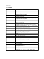
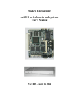
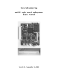
Soekris Engineering
net5501 series boards and systems.
User’s Manual
Vers 0.10 – May 16, 2012
Table of Contents
1 INTRODUCTION................................................................................................4
1.1 Overview...................................................................................................................................................5
1.2 Bus Expansion..........................................................................................................................................6
1.3 Multi-IO Controller.................................................................................................................................6
2 BIOS ..................................................................................................................6
2.1 Overview...................................................................................................................................................6
2.2 Serial Console...........................................................................................................................................6
2.3 System Startup.........................................................................................................................................6
2.4 Monitor Commands ................................................................................................................................7
2.5 BIOS System Parameters........................................................................................................................8
3 CONNECTORS AND INDICATORS..................................................................9
3.1 J5, DC Input Jack..................................................................................................................................11
3.2 J2, 3.3V PCI Connector.........................................................................................................................11
3.3 J4, PCI Riser Header.............................................................................................................................11
3.4 J3, Mini-PCI Socket ..............................................................................................................................12
3.5 JP2, CompactFlash socket ....................................................................................................................12
3.6 JP5, User I/O ..........................................................................................................................................12
3.7 JP11-JP14, Ethernet Jacks. ..................................................................................................................12
3.8 JP10, DC Power .....................................................................................................................................12
3.9 SW1, Reset..............................................................................................................................................12
3.10 JP4, COM2 ...........................................................................................................................................13
3.11 P1, COM1.............................................................................................................................................13
3.12 D2, Error LED .....................................................................................................................................13
3.13 D4, D5, D7 & D8, Network Activity LED’s .......................................................................................13
3.14 D3, Power On LED ..............................................................................................................................13
3.15 D1, Disk Activity LED.........................................................................................................................13
3.16 JP6, USB Port ......................................................................................................................................13
3.17 JP8, internal USB Connector..............................................................................................................13
3.18 J6, SATA connector.............................................................................................................................13
3.19 JP15, SATA Power ..............................................................................................................................13
3.20 J1, PATA ..............................................................................................................................................14
3.21 JP7 Internal Status Connector ...........................................................................................................14
4 SOFTWARE INSTALLATION..........................................................................14
4.1 Loading Operating System ...................................................................................................................14
4.2 Ethernet Drivers ....................................................................................................................................14
1 Introduction
This manual describes the Soekris Engineering net5501 Series of boards and systems. The net5501 is
available as a board only, or in a small sheet metal case. In both cases, they are available in different
configurations.
The net5501 is based on the Geode LX embedded processor from AMD, and is basically a PC compatible
embedded computer optimized for network and communication applications.
This manual assumes that the reader has a deep understanding of PC Architecture, and will only cover
areas specific to the net5501. Most of the net5501 functionality and interfaces are either following official
PC standards, or unofficial de-facto standards.
Specifications
1.1
Overview
Processor
Core Chipset
Multi-IO
Main Memory
BIOS
Bus Expansion
Ethernet
Serial Ports
Storage
USB Ports
Real Time Clock
Supervision
General Purpose I/O
Power Supply
Power Consumption
Environmental Conditions
EMI/EMC
Agency Compliance
Physical Size
AMD Geode LX single chip processor with CS5536 companion chip,
clocked at 433 to 500 Mhz
Integrated in the Geode LX/CS5536
NSC PC87366
128 to 1024 Mbyte DDR266 SDRAM, soldered on board.
512 Kbyte FLASH, soldered on board.
Contain Soekris Engineering comBIOS.
1-2 - PCI slot, 3.3V singnaling only, limited power available.
1 - Mini-PCI type IIIA socket.
Up to four Ethernet Controllers using the VIA VT6105M PCI busmaster
chip, supporting 10BaseT and 100BaseT.
RJ-45 Connectors at board edge with built in LED’s for link status and
network activity.
1 or 2 serial ports, using 16C550 uarts.
1 standard with PC type DB-9 connector at board edge.
1 optional with 10 pins header.
1 CompactFlash type I/II socket.
1 UltraDMA-100 interface with 44 pins connector for 2.5" Hard Drive.
1 Serial ATA 1.0 interface for Hard Drive, with +5V & +12V power header.
1 external USB 2.0 high speed port.
1 optional internal USB 2.0 high speed pin header.
Integrated in the CS5536. Backup power is provided by a rechargeable
lithium battery, which can supply power for minimum 1 month.
Watchdog timer, integrated in the CS5536.
Temperature monitor, integrated in the PC87366.
Voltage monitor, integrated in the PC87366.
12 bits of programmable input/output pins, connected directly to the
PC87366.
6 to 28V DC, 25W maximum usage, using a DC input Jack at board edge, or
5V DC, using connector on board.
Max 6W without using expansion connectors.
Operating:
0°C to 60°C temperature
10% to 90% relative humidity, non condensing.
Storage:
-20°C to 85°C temperature
5% to 95% relative humidity, non condensing.
All interfaces intended for external connections are protected against
emissions and immunity.
When using the optional metal case:
CE Marking EN55022 Class A
CE Marking EN55024
FCC Part 15 Class A
Board only: 6.30” x 6.50” (160mm x 165 mm)
Small metal case: 6.72” x 7.00” x 1.3” (171mm x 178mm x 33mm)
Wide metal case: 6.72” x 11.4” x 1.3” (171mm x 290mm x 33mm)
1.2
Bus Expansion
The net5501 has three different PCI expansion possibilities, the connector J2 is a standard 3.3V PCI v2.2
connector and J3 is a Mini-PCI type IIIA socket, and the connector J4 is a 100 pins special connector to be
used for an optional 3.3V 2nd PCI v2.2 connector using a riser board.
Please note that there is limited power available for the three PCI expansion connectors. There are only
20W available on the 3.3V power pins and 5V pins combined. If a 2.5” hard disk is used, it will also need
to share the available power.
An onboard DC-DC converter supplies +12V @ 0.3A and –12V @ 0.1A to the PCI connector. If the board
is powered by 12V then a bypass circuit will supply up to 1A of the 12V to the PCI connector.
CAUTION: Please note that the Standard PCI connector is a 3.3V signaling only connector, and is
keyed for that. Do not insert a 5V PCI expansion board upside down, that can cause permanent damage to
both the net5501 and the expansion board.
1.3
Multi-IO Controller
The net5501 has an onboard Multi-IO controller which provide the two serial ports, Voltage and
Temperature monitor and the GPIO pins. The Multi-IO controller is connected via the LPC bus and its
configuration register index/data pair is located at hex 2E and 2F. The comBIOS program all the base
address locations, but the actual addresses need to be determined by reading the Multi-IO configuration
registers.
2 BIOS
2.1
Overview
The net5501 comes with the Soekris Engineering netBIOS. The BIOS is designed especially for setup and
operation using the serial port as the console. The BIOS is located in Flash memory, and can be upgraded
over the serial port. Critical system setup parameters are also saved in the Flash memory, so the system will
not lose any setup information due to CMOS battery backup power loss.
2.2
Serial Console
The net5501 does not have any video or keyboard interface, and uses the COM1 serial port for the primary
console interface instead. The serial port default baud rate is 19200, but it can be changed by the monitor
“set” command. The netBIOS also has an emulation of int10 video system calls and int16 keyboard system
calls, making it possible to run old real mode programs that expect video and keyboard services. This is
mostly useful for running MS-DOS, and is limited to software using the BIOS calls only. The serial port
connector is a standard PC type 9 pins D-SUB, so a serial crossover cable should be used when connecting
to another PC.
The connected ANSI/VT100 terminal or terminal emulator should be set for 19200 baud, 8 databits, no
parity, 1 stop bit, no flow control.
2.3
System Startup
When the net5501 is powered up or rebooted, the netBIOS will first display diagnostic checkpoint codes on
the serial console. When it has located and checked the first 64 Kbytes of main memory, it will display a
sign on message and then continue with additional testing and configuration. After that, it will start a short
countdown before it will try to boot an operating system. During the countdown time, by pressing Ctrl-P,
the normal boot process can be interrupted and control transferred to the comBIOS’s monitor program. The
monitor is a command line driven program for setup and light diagnostic and debugging. Typing “?” or
“help” at the command prompt will show a short list of commands available.
Note that after changing system parameters using the “set” command, it will be necessary to restart the
system before the new parameters will be used, by using the “reboot” command.
2.4
Monitor Commands
boot [drive]
Load operating system from a boot device, using int19 system call. Drive can either be a valid int13 drive
entered as a hexadecimal number, or a special number. For example “80” will be first fixed disk drive,
normally the CompactFlash on the net5501, and that is also the default if no parameter is entered. Currently
defined special number is “F0”, which will try to boot over the network, using the PXE boot ROM.
reboot
Will reboot the BIOS, normally used after changing system parameters.
download
Start downloading a binary image over the serial ports, using the XMODEM protocol. After entering the
command, start sending at the terminal program at the other end. Will time out after 30 seconds if it does
not detect the start of a XMODEM transfer. Downloaded binary image will be saved in memory at
4000:0000. Since BIOS v. 1.22 the download command defaults to CRC. By entering “download -” it's
possible to revert to checksum.
flashupdate
Update the system flash BIOS with image at 4000:0000, normally the one just downloaded using the
“download” command.
time [HH:MM:SS]
Update the time in the battery backed Real Time Clock, or if no parameter, show the current date and time.
The time should be entered in 24 hours format, as “hour:minutes:seconds”.
date [YYYY/MM/DD]
Update the date in the battery backed Real Time Clock, or if no parameter, show the current date and time.
The date should be entered as “year/months/date”.
set parameter=value
Set a BIOS system parameter to a value. See section 2.5 for a list of currently available parameters to set.
Note that a reboot is required after changing most parameters before the new value will be used.
show [parameter]
Show the current value of a parameter, or if no parameter, show a list of all parametes and their current
value.
d[b|w|d] [adr]
List the content of the memory, in both ascii and hexadecimal. “db” will show it as 8 bit bytes, “dw” will
show it as 16 bit words and “dd” will show it as 32 bit doublewords. “adr” is a memory address in
hexadecimal, either in 16 bit seg:offset format or as a single linear 32 bit address. If no address is entered, it
will continue listing from last address, if “d” is entered alone, it will list in the last used format.
i[b|w|d] port
Input and show the content of a port address. “ib” will input a 8 bit byte, “iw” will input a 16 bit word and
“id” will input a 32 bit double word. The port address is in hexadecimal from 0 to FFFF.
o[b|w|d] port value
Output a value to a port address. “ob” will output a 8 bit byte, “ow” will output a 16 bit word and “od” will
output a 32 bit double word. The port address is in hexadecimal from 0 to FFFF, and the value is a
hexadecimal number.
e[b|w|d] addr value [...]
Enter values in memory. “eb” will enter a 8 bit byte, “ew” will enter a 16 bit word and “ed” will enter a 32
bit double word. “adr” is a memory address in hexadecimal, either in 16 bit seg:offset format or as a single
linear 32 bit address.
2.5
BIOS System Parameters
ConSpeed
Serial Console speed baud rate. Value can be 2400, 4800, 9600, 19200, 38400 or 57600, default is 19200.
ConLock
Protecting the serial console port from modifications using int14 system calls. Value can be “enabled” or
“disabled”, default is “enabled”. Useful for preventing MS-DOS from changing the console speed on start
up.
ConMute
Console port is muted during POST. Value can be “enabled” or “disabled”, default is “disabled”. Ctrl-P can
still be used for entering monitor.
BIOSentry
To control if the “Press Ctrl-P for entering Monitor.” message should be displayed during before booting.
Value can be “enabled” or “disabled”, default is “enabled”. Useful for making it harder for end users to
enter the monitor and modify BIOS settings. Note that pressing “Ctrl-P” will still work for entering the
monitor.
PCIROMS
To control if the BIOS will execute code found in PCI expansion ROM’s. Value can be “enabled” or
“disabled”, default is “enabled”. Can be used to disable problematic ROM’s on PCI boards, or to shorten
the BIOS boot time. If this is disabled you cannot use PXE.
PXEBoot
Enable automatic PXE booting at startup. Value can be “enabled” or “disabled”, default is “enabled”. This
does not influence manual PXE booting via "boot f0".
FLASH
To set the disk channel of the onboard CompactFlash socket. Value can be “primary” or “secondary”,
default is “primary”. Useful if the system is used with an external IDE controller.
BootDelay
To set the delay time before booting an operating system. Value can be from 2 to 16 seconds, default is 5
seconds.
FastBoot
Cuts POST to about 2 seconds. Value can be “enabled” or “disabled”, default is “enabled”. Warning: You
then need to be quick with ctrl-P to enter the monitor.
BootPartition
Sets which partition to boot from. If set to Disabled, boot using Disk MBR. If set to a number from 1 to 4,
boot directly from that partition, bypassing the Disk MBR.
BootDrive
Which devices to boot from and in what order. Option are 80=first drive/hd0, 81=second drive/hd1,
F0=PXE/network.
You can add up to 4 options and empty options will be shown as "FF". Default is “80 81 F0 FF”.
ShowPCI
Enabling showing list of PCI devices at startup. Value can be “enabled” or “disabled”, default is “enabled”.
Reset
Sets the reset button to either hard or soft reset. Value can be “Soft” or “Hard”, default is “Hard”.
CpuSpeed
Change CPU clock speed. Value can be “default” or “xxx”, default is “default”. “xxx”=200-cpumax+33.
3 Connectors and Indicators
The following sections provide pin definitions and descriptions of all onboard connectors and LED
indicators. Some of the connectors are on located along one edge of the board, and are designed for access
though the rear of the optional sheet metal case. The LED indicators are located along the opposite board
edge, and are designed to be viewed from the front of the case.
3.1
J5, DC Input Jack
The 2.1mm DC Power Jack should be used for connecting a small wall mount unregulated power adapter,
supplying 6V-28V DC at 15 VA, with a 5.5mm outside, 2.1mm inside female power plug with plus at
center pin. It is protected against reverse polarity. Please note that standard unregulated power transformers
can supply much higher voltage that the specified nominal voltage, so when using such a type it’s
recommended to use one that is specified for 16V DC or less.
3.2
J2, 3.3V PCI Connector
PCI rev 2.2 connector, please see the PCI Specification rev 2.2 for pin layout and electrical specifications.
Also, please see the “Bus Expansion” section for limitations.
3.3
J4, PCI Riser Header
100 pins special connector to be used for an optional 3.3V 2nd PCI v2.2 connector using a riser board.
3.4
J3, Mini-PCI Socket
Mini-PCI type IIIA socket, please see the Mini-PCI Specification rev 1.0 for pin layout and electrical
specifications, also, please see the “Bus Expansion” section for limitations.
3.5
JP2, CompactFlash socket
CompactFlash type I/II socket. This interfaces to the Geode LX processor as an IDE controller, and can be
set for either the master or slave on the controller. Please see the Compact Flash Specification rev 1.4 for
pin layout, mechanical and electrical specifications.
3.6
JP5, User I/O
20 pins 0.050” header with 12 programmable general purpose input/output pins and com2 serial port access
at TTL level. They are connected directly to the PC87366 Multi-IO controller, please see the PC87366
datasheet for programming information and electrical specifications. When the board is viewed as on the
illustration, pin 1 is the top left pin, at the “JP5” text.
PC87366 Pin
-GPIO20, 117
GPIO22, 119
GPIO24, 121
GPIO26, 123
-GPIO5, 7
GPIO13, 55
SOUT2, 107
3.7
Function
+3.3V Power
GPIO 0
GPIO 2
GPIO 4
GPIO 6
GND
GPIO 9
GPIO 10
GND
TXD
Pin Number
1
2
3
4
5
6
7
8
9
10
11
12
13
14
15
16
17
18
19
20
Function
+5V Power
GPIO 1
GPIO 3
GPIO 5
GPIO 7
GPIO 8
GND
GPIO 11
RXD
GND
PC87366 Pin
-GPIO21, 118
GPIO23, 120
GPIO24, 122
GPIO26, 124
GPIO4, 6
-GPIO12, 54
SIN2, 105
JP11-JP14, Ethernet Jacks.
8 pins shielded RJ-45 jacks with built in LED’s for link status and network activity. Auto detects between
10baseT or 100baseT. When viewed from the rear, the left LED is link status, will be yellow when set for
10baseT and green when set for 100baseT, and the right LED will be green if there is network activity.
When software uses the BIOS PCI functions for searching for PCI devices, JP11 will be the first found, the
JP12, JP13 and JP14.
3.8
JP10, DC Power
6 pins AMP MTA100 header, for connecting of internal power supply. Also has 2 of the GPIO pins, for use
with advanced power management. Can be used with a 5V DC power supply if pin 3 and 4 are connected
together, or with a 6V to 28V DC power supply if only pin 3 are used. When the board is viewed as on the
illustration, pin 1 is the top pin, at the JP10 text.
Function
GND
GND
VPWR
+5V
GPIO 4
GPIO 0
3.9
Pin Number
1
2
3
4
5
6
SW1, Reset
Small switch, usually accessible though a small hole in the case. Can be selected to work either as a “hard”
processor reset or as a “soft” software readable reset.
3.10 JP4, COM2
10 pins 0.050” header for serial port COM2. Can be connected to a DB9 using a de facto standard cable
assembly. When the board is viewed as on the illustration, pin 1 is the top left pin, at the “JP4” text.
DB9 Pin
1
2
3
4
5
Function
DCD
RXD
TXD
DTR
GND
Pin Number
1
2
3
4
5
6
7
8
9
10
Function
DSR
RTS
CTS
RIN
+5V Power
DB9 Pin
6
7
8
9
3.11 P1, COM1
9 pins DB9 connector for serial port COM1. The pinout follow the de facto standard for DB9 PC serial
ports. Normally used for serial management console.
3.12 D2, Error LED
This red LED is connected to the PC87366 Multi-IO controller GPIO6, pin D9. It is connected so that it
will be on at power on, and can then be turned off and on by software control. When programming GPIO6
with a 0, it will be off. The BIOS will normally turn it off just before booting an operating system.
3.13 D4, D5, D7 & D8, Network Status/Activity LED’s
These Green LED’s will indicate status for each ethernet port, a LED will be on when the Link is ok, it will
flash brighter when there is traffic.
3.14 D3, Power On LED
This green LED will be on when there is applied power to the board.
3.15 D1, Disk Activity LED
This yellow LED will be on when there is disk activity, either by the CompactFlash module or the optional
Hard Disk.
3.16 JP6, USB Port
USB 2.0 external port.
3.17 JP8, internal USB Connector
Second USB connector, standard USB extension cable pinout.
JP8 Pin
1
2
3
4
Function
+5V
DataData+
GND
3.18 J6, SATA connector
Serial ATA 1.0 PATA to SATA bridge interface for SATA Harddrives.
3.19 JP15, SATA Power
4-pin MTA100 connector. Matches 3.5" floppy disk power pinout.
JP15 Pin
1
2
3
4
Function
+12V
GND
GND
+5V
3.20 J1, PATA
UltraDMA-100 interface with 44 pins connector for 2.5" Hard Drive.
3.21 JP7 Internal Status Connector
4-pin single-row header for status LEDS.
JP7 Pin
1
2
3
4
Function
+3.3V
Power
Error
Disk Activity – low when active
4 Software Installation
4.1
Loading Operating System
The net5501 can use SATA disks, PATA disks or CF Flash disk for permanent program and data storage.
There are two ways of loading software on the storage device.
•
Booting an install program using the PXE boot ROM, and then installing the rest over the network.
Only some operating systems support PXE booting and/or installation over the network.
•
Preloading the storage device on another system. The net5501 uses a simple algorithm for sector
translation for storage devices, if there are less than 1024 tracks, it will use the native CHS that the
device reports, if more than 1024 tracks, it will use LBA translation. So the host system will need to
match that, and that will also normally be the case. In some cases it may be necessary to change the
translation settings in the host system’s BIOS or to do manually configuration of the boot loader used.
4.2
Ethernet Drivers
The used VIA VT6105M ethernet controller is directly supported by the newer versions of most operating
systems, and will normally be automatically detected. As it is a relatively new chip, it may be necessary to
upgrade to the newest version, or to locate device drivers. For most operating systems, drivers are available
on VIA’s website at http://www.via.com.tw/en/products/networking