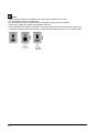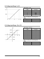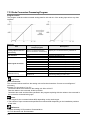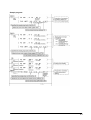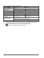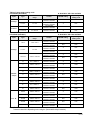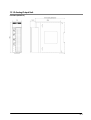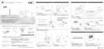
1
Safety Precautions Observe the following notices to ensure personal safety or to prevent accidents. To ensure that you use this product correctly, read this User’s Manual thoroughly before use. Make sure that you fully understand the product and information on safety. This manual uses two safety flags to indicate different levels of danger. WARNING If critical situations that could lead to user’s death or serious injury is assumed by mishandling of the product. -Always take precautions to ensure the overall safety of your system, so that the whole system remains safe in the event of failure of this product or other external factor. -Do not use this product in areas with inflammable gas. It could lead to an explosion. -Exposing this product to excessive heat or open flames could cause damage to the lithium battery or other electronic parts. CAUTION If critical situations that could lead to user’s injury or only property damage is assumed by mishandling of the product. -To prevent excessive exothermic heat or smoke generation, use this product at the values less than the maximum of the characteristics and performance that are assured in these specifications. -Do not dismantle or remodel the product. It could cause excessive exothermic heat or smoke generation. -Do not touch the terminal while turning on electricity. It could lead to an electric shock. -Use the external devices to function the emergency stop and interlock circuit. -Connect the wires or connectors securely. The loose connection could cause excessive exothermic heat or smoke generation. -Do not allow foreign matters such as liquid, flammable materials, metals to go into the inside of the product. It could cause excessive exothermic heat or smoke generation. -Do not undertake construction (such as connection and disconnection) while the power supply is on. It could lead to an electric shock. Copyright / Trademarks -This manual and its contents are copyrighted. -You may not copy this manual, in whole or part, without written consent of Panasonic Industrial Devices SUNX Co., Ltd. -Windows is a registered trademark of Microsoft Corporation in the United States and other countries. -All other company names and product names are trademarks or registered trademarks of their respective owners. PLC_ORG Table of Contents Precautions Before You Start 1 Functions and Restrictions of the Unit .................................................. 1-1 1.1 Features and Functions of the Unit ............................................................................... 1-2 1.2 Type of Unit ...................................................................................................................... 1-3 1.3 Analog I/O Data Processing Functions ......................................................................... 1-4 1.3.1 Analog Input ................................................................................................................ 1-4 1.3.2 Analog Output Processing .......................................................................................... 1-5 1.4 Installation Restrictions .................................................................................................. 1-6 1.4.1 Installation Position of Analog Input Unit and Output Unit .......................................... 1-6 1.5 Current Consumption...................................................................................................... 1-7 2. Parts and Functions ............................................................................... 2-1 2.1 Analog Input Unit ............................................................................................................. 2-2 2.1.1 Analog Input Unit (FP2-AD8VI) ................................................................................... 2-2 2.1.2 Analog Input Unit (Channel isolation type) (FP2-AD8X) ............................................. 2-3 2.1.3 RTD Input Unit (FP2-RTD).......................................................................................... 2-4 2.2 Analog Output Unit (FP2-DA4) ....................................................................................... 2-5 3. Wiring....................................................................................................... 3-1 3.1 Wiring of Terminal Block ................................................................................................ 3-2 3.1.1 Input Unit (FP2-AD8X) (FP2-RTD) ............................................................................. 3-2 3.1.2 Input Unit (FP2-AD8VI)/Output Unit (FP2-DA4) ......................................................... 3-5 3.2 Wiring for Analog Input ................................................................................................... 3-6 3.2.1 Analog Input Unit (FP2-AD8VI) ................................................................................... 3-6 3.2.2 Analog Input Unit (FP2-AD8X) .................................................................................... 3-7 3.2.3 RTD Input Unit (FP2-RTD)........................................................................................ 3-10 3.3 Wiring for Analog Output .............................................................................................. 3-11 3.3.1 Analog Output Unit (FP2-DA4) ................................................................................. 3-11 4. Setting I/O Range and I/O Allocation..................................................... 4-1 4.1 I/O Allocation .................................................................................................................... 4-2 4.1.1 Setting the Analog Input Range .................................................................................. 4-2 4.1.2 Setting the Analog Output Range ............................................................................... 4-3 i 4.2 I/O Allocation and Slot Numbers .................................................................................... 4-4 4.2.1 Occupation I/O Areas and I/O Allocation .................................................................... 4-4 4.2.2 Confirmation of I/O No. Allocation ............................................................................... 4-5 4.2.3 Slot Numbers .............................................................................................................. 4-6 5. Power On/Off and Initial Settings .......................................................... 5-1 5.1 Unit Operation When turning the Power On/Off ........................................................... 5-2 5.1.1 Analog Input Operation ............................................................................................... 5-2 5.1.2 Analog Output Operation ............................................................................................ 5-2 5.2 Initial Setting Programs .................................................................................................. 5-3 5.2.1 Input Settings .............................................................................................................. 5-3 5.2.2 Output Settings ........................................................................................................... 5-4 6. Analog I/O Conversion Characteristics................................................. 6-1 6.1 Analog Input Conversion Characteristics ..................................................................... 6-2 6.1.1 Current Input Range: 4 to 20 mA ................................................................................ 6-2 6.1.2 Current Input Range: -20 to +20 mA ........................................................................... 6-2 6.1.3 Voltage Input Range: 1 to 5 V ..................................................................................... 6-3 6.1.4 Voltage Input Range: -10 to +10 V.............................................................................. 6-3 6.1.5 Voltage Input Range: -100 to +100 mV ...................................................................... 6-4 6.1.6 Thermocouple Input Range ........................................................................................ 6-5 6.1.7 R.T.D. (Resistance Thermometer Device) Input Range ............................................. 6-6 6.2 Analog Output Conversion Characteristics .................................................................. 6-7 6.2.1 Voltage Output Range: -10 to +10 V ........................................................................... 6-7 6.2.2 Current Output Range: 0 to 20 mA ............................................................................. 6-7 7. Basics of Analog Input ........................................................................... 7-1 7.1 Reading the Analog Input Data ...................................................................................... 7-2 7.1.1 Reading the Analog Input Data ................................................................................... 7-2 7.2 Timing for Reading Data ................................................................................................. 7-3 7.3 Sample Program .............................................................................................................. 7-4 7.3.1 Basic Program (Analog Input Unit) ............................................................................. 7-4 7.3.2 Scale Conversion Processing Program ...................................................................... 7-6 8. Optional Settings for Analog Input ........................................................ 8-1 8.1 Average Processing Setting ........................................................................................... 8-2 8.1.1 Average Processing for Analog Unit ........................................................................... 8-2 8.1.2 Sample Program ......................................................................................................... 8-4 8.1.3 Offset Setting Program................................................................................................ 8-6 8.2 Temperature Sensor Input Broken Wire Detection ...................................................... 8-8 8.2.1 Broken Wire Detection for Analog Unit ....................................................................... 8-8 ii 8.2.2 Sample Program ......................................................................................................... 8-9 9. Basics of Analog Output ........................................................................ 9-1 9.1 Writing the Analog Output Data ..................................................................................... 9-2 9.2 Sample Program .............................................................................................................. 9-3 9.2.1 Basic Program (Analog Output Unit)........................................................................... 9-3 10. Optional Settings for Analog Output................................................. 10-1 10.1 Analog Output Hold Setting ....................................................................................... 10-2 10.2 Sample Program .......................................................................................................... 10-3 10.2.1 Final Value of Run Mode ........................................................................................ 10-3 10.2.2 Output Hold (Any Value) Setting (Analog Output Unit) ........................................... 10-4 11. Troubleshooting .................................................................................. 11-1 11.1 Troubleshooting (Analog Input) ................................................................................. 11-2 11.1.1 Analog Input Value Cannot be Read ...................................................................... 11-2 11.1.2 Analog Input Conversion Value is Unsteady .......................................................... 11-2 11.1.3 Proper Current Input Conversion Value Cannot be Obtained ................................ 11-2 11.1.4 Proper conversion Value Cannot be Obtained During Thermocouple Connection 11-2 11.1.5 Proper conversion Value Cannot be Obtained During R.T.D. Connection ............. 11-2 11.2 Troubleshooting (Analog Output) .............................................................................. 11-3 11.2.1 Analog Output Value is Unsteady ........................................................................... 11-3 11.2.2 Analog Output Value Does Not Change ................................................................. 11-3 12. Specifications ..................................................................................... 12-1 12.1 Table of Specifications ............................................................................................... 12-2 12.1.1 Table of Input/Output Contact Allocation ................................................................ 12-7 12.2 Table of Shared Memory Area .................................................................................... 12-8 12.2.1 Shared Memory of Analog Input Unit ...................................................................... 12-8 12.3 Analog I/O Conversion Cycle Time .......................................................................... 12-14 13. Dimensions, Sample Programs and others ...................................... 13-1 13.1 Dimensions .................................................................................................................. 13-2 13.1.1 Analog Input Unit..................................................................................................... 13-2 13.1.2 Analog Output Unit .................................................................................................. 13-3 13.2 Sample Programs ........................................................................................................ 13-4 13.2.1 Temperature Control by PID Operation .................................................................. 13-4 iii Precautions Before You Start Differences with the conventional unit Input type Voltage Current Thermocouple Type Measurement range A:Available Remarks (between channels) Non-isolated FP2-AD8 FP2-AD8VI FP2-AD8X FP2-RTD AFP2400 AFP2400L AFP2401 AFP2402 A A A 10 V -10 to +10 V 1 to 5 V 1 to 5 V 100 mV -100 to +100 mA 20 mA -20 to +20 mA Non-isolated 4 to 20 mA 4 to 20 mA Non-isolated S 0 to +1500 C A A J -200 to +750 C A A J -100 to 400 C K -200 to +1000 C K -200 to 1200 C K -100 to 600 C T -200 to +350 C R 0 to +1500 C Isolated Non-isolated A A A Isolated Non-isolated A A Isolated Non-isolated (FP2-AD8) A A A A A A A A A Isolated (FP2-AD8X) A A A A A A A N -200 to 1300 C Pt100 -100 to +500 C Resistance Pt100 -200 to +650 C A A thermo- Pt100 -100 to 200 C A A meter JPt100 -200 to +650 C A A A A A A device JPt100 -100 to 200 C Pt1000 -100 to +100 C A A Non-isolated A About a similar manual For FP2 Analog Input Unit, there are two manuals, which is for FP2-AD8 (traditional type), and for FP2AD8VI, AD8X and RTD (new type). The appropriate manual must be referred to use each product. (Two manuals for FP2 Analog Output Unit FP2-DA4 include the same contents.) Manual Name Manual No. Relevant models This manual Traditional manual FP2 New Analog Unit FP2 Analog Unit ARCT1F397 ARCT1F283 FP2-AD8VI,FP2-AD8X,FP2-RTD FP2-AD8 Current input with FP2-AD8X If inputting current with FP2-AD8X, install the provided resistor between the “B/-“ terminal and the “V/b” terminal, and input after converting it to voltage. Reference: <3.2.2 Analog Input Unit (FP2-AD8X)> For further details, refer to the specifications in the following manuals before you use. FP/FP2SH Hardware Manual ARCT1F320 FP series Programming Manual ARCT1F353 iv Chapter 1 Functions and Restrictions of the Unit 1.1 Features and Functions of the Unit Features of analog input unit • This is a unit to import various analog values (such as voltage, current or temperature) of displacement sensors or pressure sensors, and to convert them to digital values in the unit. • Input with multiple channels is available. Analog input unit: 8 channels Twenty types of input range such as voltage and temperature sensor are selectable and available for various connection devices.(FP2-AD8X) • Resistance thermometer device and thermocouple can be directly connected. (FP2-AD8X, FP2-RTD) • High-speed conversion of 500 µs/channel for voltage/current range, etc. • The resolution is 1/13107 to 1/65536 (temperature sensor is 0.1 °C. The input analog values are converted to a maximum of 16-bit digital data. Features of analog output unit • This is a unit to convert the data within the unit to analog values, and to output them to analog drive devices such as inverter. • Two types of output range are available (voltage: -10 V to +10 V and current: 0 to 20 mA). Analog output unit: 4 channels High-speed D/A conversion of 500 µs/channel. • The resolution is 1/4096 and the data to output is treated as 12-bit digital data. 1-2 1.2 Type of Unit Name FP2 analog input unit (Voltage/current type) FP2 analog input unit (Channel isolation type) FP2 RTD input unit FP2 Analog output unit No. of channels Part No. Product No. Input 8 chs FP2-AD8VI AFP2400L Input 8 chs FP2-AD8X AFP2401 Input 8 chs Output 4 chs FP2-RTD FP2-DA4 AFP2402 AFP2410 1-3 1.3 Analog I/O Data Processing Functions 1.3.1 Analog Input The following process is performed. 1. Loading of analog input The analog input data of the displacement sensor or pressure sensor are taken in the input part of the analog unit. 2. Digital conversion The analog input values are automatically converted to digital values successively in the unit. 3. Storage of digital values The converted digital values are read by the user program as the data of the input relay area (WX). For the analog input, the following optional settings are available. The optional settings can be specified by writing into the shared memory using the programs for each channel if necessary. Setting for No. of times of averaging Sets the number of times to average the converted data. Setting for temperature sensor broken wire detection Sets to detect the disconnection of the input wiring for the input channels which has been set to the temperature sensor range (thermocouple input range and resistance thermometer device). 1-4 1.3.2 Analog Output Processing The following process is performed. 1. Writing of digital data The digital data for the analog output are written in the output relay area (WY) corresponding to each channel by the user program. 2. Analog conversion The written data are automatically converted to analog values successively in the unit. 3. Output to analog drive devices The converted analog values are output to analog drive devices such as inverter. For the analog output, the following optional settings are available. The optional settings can be specified by writing into the shared memory using the programs for each channel if necessary. Analog output hold setting Sets to either “not hold”, “hold” or “hold (any value)” when changing to the FP2 CPU unit PROG. mode. 1-5 1.4 Installation Restrictions 1.4.1 Installation Position of Analog Input Unit and Output Unit Can be installed in any slots on the CPU backplane and the expansion backplane except the slots for the power supply unit and the CPU unit. 1-6 1.5 Current Consumption The internal current consumption values for the FP2 analog units noted below. When the system is configured, the other units being used should be taken into consideration, and a power supply unit with a sufficient capacity should be used. Name FP2 analog input unit (Voltage/current type) FP2 analog input unit (Channel isolation type) FP2 RTD input unit FP2 Analog output unit Part No. Product No. Current consumption (at 5 V DC) FP2-AD8VI AFP2400L 400 mA or less FP2-AD8X AFP2401 300 mA or less FP2-RTD FP2-DA4 AFP2402 AFP2410 300 mA or less 600 mA or less Reference: For information on the internal current consumption of other units, see <FP2/FP2SH User’s Manual ARCT1F320>. 1-7 1-8 1-9 Chapter 2 Parts and Functions 2.1 Analog Input Unit 2.1.1 Analog Input Unit (FP2-AD8VI) AFP2400L 1. Analog input terminals There are analog input terminals for channels 0 to 7. The terminal block can be removed to facilitate wiring. M3 solderless terminals can be used. 2. Range setting switch Used to set the analog input range. 2-2 2.1.2 Analog Input Unit (Channel isolation type) (FP2-AD8X) AFP2401 1. Analog input terminals There are analog input terminals for channels 0 to 7. The terminal block can be removed. The wiring connections should be carried out with the terminal block removed. If it is hard to remove the terminal block, insert a driver for the terminal block into a gap between the terminal block and the case to remove the block. Reference: <3.1 Wiring of Terminal Block> 2. Range setting switch Used to set the analog input range. 2-3 2.1.3 RTD Input Unit (FP2-RTD) AFP2402 1. Analog input terminals There are analog input terminals for channels 0 to 7. The terminal block can be removed. The wiring connections should be carried out with the terminal block removed. If it is hard to remove the terminal block, insert a driver for the terminal block into a gap between the terminal block and the case to remove the block. Reference: <3.1 Wiring of Terminal Block> 2. Range setting switch Used to set the analog input range. 2-4 2.2 Analog Output Unit (FP2-DA4) AFP2410 1. Analog output terminals There are analog output terminal for 4 channels. Terminals with a dot mark are not used; however, they are connected to the analog input circuit internally so do not connect anything to them. The terminal block can be removed to facilitate wiring. M3 solderless terminals can be used. 2. Range setting switch Used to set the analog output range. 2-5 2-6 Chapter 3 Wiring 3.1 Wiring of Terminal Block 3.1.1 Input Unit (FP2-AD8X) (FP2-RTD) A screw-down connection type for terminal block is used. The suitable wires are given below. Terminal block socket Item Number of pin Manufacturer Model No. Product No. Suitable wires No. of wires 1 wire 2 wires Description 16 pins Phoenix Contact Co. MC1,5/16-ST-3,5 1840502 Size AWG #28 to 16 AWG #28 to 20 Nominal cross-sectional area 0.08 to 1.25mm2 0.08 to 1.5mm2 Pole terminal with a compatible insulation sleeve If a pole terminal is being used, the following models manufactured by Phoenix Contact Co. should be used. Part No. Cross-sectional Manufacturer Size Without insulating 2 area (mm ) With insulating sleeve sleeve 0.25 AWG #24 AI 0,25-6 BU A 0,25-7 0.34 AWG #22 AI 0,34-6 TQ A 0,34-7 0.50 AWG #20 AI 0,5-6 WH A 0,5-6 Phoenix 0.75 AWG #18 AI 0,75–6 GY A 0,75-6 Contact Co. 1.00 AWG #18 A 1-6 0.52 AWG #20 AI-TWIN 2X 0,5-8 WH (for 2 pcs) Pressure welding tool for pole terminals Manufacturer Part No. Phoenix Contact Co. CRIMPFOX 6 Product No. 1212034 For tightening the terminal block When tightening the terminals of the terminal block, use a screwdriver (Phoenix contact Co., Product No. 1205037) with a blade size of 0.4 2.5 (Part No. SZS 0,42,5). The tightening torque should be 0.22 to 0.25 N・m (2.3 to 2.5 kgf・cm) or less. 3-2 Wiring method (1) Remove the terminal block. If it is hard to remove, insert a driver for the terminal block into a gap between the terminal block and the case, and remove the terminal block 1. Firstly, remove the terminal block at the side of ch4 to ch7. Insert the driver into the ch4 side and ch7 alternately. 2. Remove the terminal block at the side of ch0 to ch3. At this time, take care not to damage a temperature sensor located in the center of the terminal block. (2) Remove a portion of the wire’s insulation. (3) Insert the wire into the terminal block until it contacts the back of the block socket, and then tighten the screw clockwise to fix the wire in place. (Tightening torque: 0.22 N·m to 0.25 N·m (2.3 kgf·cm to 2.5 kgf·cm)) When using FP2-AD8X as current input If 250Ω resistor is connected, 4 to 20 mA is converted to 1 to 5V, and –20 to +20 mA is converted to –5V to +5V. • Crimp the provided resistor and the wiring using a pole terminal manufactured by Phoenix Contact Co. (AI-TWIN2X0.5-8WH), and then connect to the terminal block. Use the wiring of which size is AWG22 2 2 (cross-sectional area: 0.33 mm ) or AWG20 (cross-sectional area: 0.5 mm ). • When the pole terminal is not used, the tensile strength can be increased by winding the lead of the resistor round the wiring. Specifications of resistor for current input • Resistance value 250Ω • Rated power 0.25 W • TCR ±25 ppm/°C • Resistance value tolerance ±0.1% (4) Insert the terminal block into the unit firmly. 3-3 Note: • When removing the wire’s insulation, be careful not to scratch the core wire. • Do not twist the wires to connect them. • Do not solder the wires to connect them. The solder may break due to vibration. • After wiring, make sure stress is not applied to the wire. • In the terminal block socket construction, if the wire closes upon counter-clockwise rotation, the connection is faulty. Disconnect the wire, check the terminal hole, and then re-connect the wire. 3-4 3.1.2 Input Unit (FP2-AD8VI)/Output Unit (FP2-DA4) Suitable terminals and wires M3 terminal screws are used for the terminals of analog input and output units. The following suitable solderless terminals are recommended for the wiring to the terminals Suitable solderless terminals Manufacturer JST Mfg. Co., Ltd. Shape Round type Fork type Round type Fork type Part No. 1.25-MS3 1.25-B3A 2-MS3 2-N3A 2 Suitable wires (mm ) 0.25 to 1.65 1.04 to 2.63 Suitable wires Suitable wires 2 AWG22 to 14 (0.3 to 2.0mm ) Tightening torque 0.5 to 0.6 N・m Wiring to terminal block Remove the terminal block before beginning the wiring operations. To remove the terminal block, push downward on the release lever located at the top of the terminal block. Note: Install the terminal block by inserting it all the way to its original position and pressing the lock button on the bottom of the unit. Then confirm that the terminal block is securely attached and cannot be removed. Accessory terminal blocks can be purchased separately. Accessory terminal block for FP2 I/O unit AFP2800 (5-pack) 3-5 3.2 Wiring for Analog Input 3.2.1 Analog Input Unit (FP2-AD8VI) Voltage input (1 to 5 V, -10 to +10 V) Current input (4 to 20 mA, -20 to +20 mA) The voltage (approx. –10V) may be output momentarily (for approx. 200 ms) from the output terminal of the analog output unit when the power supply of FP2/FP2SH turns on/off. If it becomes a problem on the system, take appropriate measures, such as delaying the timing of the power activation of connected external devices from the power activation of the PLC. Note: • Use double-core twisted-pair shielded wires. It is recommended to ground them. However, depending on the conditions of the external noise, it may be better not to ground the shielding. • Do not have the analog input wiring close to AC wires, power wires, or load wires from sources other than the PLC. 3-6 3.2.2 Analog Input Unit (FP2-AD8X) Voltage input (1 to 5 V, -10 to +10 V, -100 to +100 mV) Note: • Use double-core twisted-pair shielded wires. It is recommended to ground the shielding. However, depending on the conditions of the external noise, it may be better not to ground the shielding. • Do not have the analog input wiring close to AC wires, power wires, or load wires from sources other than the PLC. Thermocouple (J, K, R, S, T, N) Note: • Perform the wiring correctly according to the polarity of the thermocouple. Also, to lengthen the signal wire of the thermocouple, use the compensating wire of the thermocouple. (It is recommended to use shielded wires and to ground the shielding.) • Do not have the analog input wiring close to AC wires, power wires, or load wires from sources other than the PLC. 3-7 R.T.D. (Resistance thermometer device) (Pt100, JPt100, Pt1000) Note: • For copper wiring used in wiring the R.T.D. (resistance thermometer device), use insulated and thick wiring not to allow a large build-up in electrical resistance. (It is recommended to use shielded wires and to ground the shielding.) • Do not have the analog input wiring close to AC wires, power wires, or load wires from sources other than the PLC. 3-8 Current input (4 to 20 mA, -20 to +20 mA) When using FP2-AD8X as current input, connect the provided 250Ωresistor, and then input after converting it to voltage. Note: When using FP2-AD8X as current input If 250Ω resistor is connected, 4 to 20 mA is converted to 1 to 5V, and –20 to +20 mA is converted to –5V to +5V. • Crimp the provided resistor and the wiring using a pole terminal manufactured by Phoenix Contact Co. (AI-TWIN2X0.5-8WH), and then connect to the terminal block. Use the wiring of which size is AWG22 2 2 (cross-sectional area: 0.33 mm ) or AWG20 (cross-sectional area: 0.5 mm ). • When the pole terminal is not used, the tensile strength can be increased by winding the lead of the resistor round the wiring. Specifications of resistor for current input • Resistance value 250Ω • Rated power 0.25 W • TCR ±25 ppm/°C • Resistance value tolerance ±0.1% 3-9 3.2.3 RTD Input Unit (FP2-RTD) R.T.D. (Resistance thermometer device) input (Pt100, JPt100, Pt1000) Note: • For copper wiring used in wiring the R.T.D. (resistance thermometer device), use insulated and thick wiring not to allow a large build-up in electrical resistance. (It is recommended to use shielded wires and to ground the shielding.) • Do not have the analog input wiring close to AC wires, power wires, or load wires from sources other than the PLC. 3-10 3.3 Wiring for Analog Output 3.3.1 Analog Output Unit (FP2-DA4) Voltage output (-10 to +10 V) Current output (0 to 20 mA) Note: • For the analog output wiring, always use double-core twisted-pair shielded wires. • Ground the shielding of the shielded wires at the side of the load devices. However, depending on the conditions of the external noise, it may be necessary to ground externally, or better not to ground the shielding. • Do not have the analog input wiring close to AC wires, power wires, or load wires from sources other than the PLC. • The terminals marked with a dot on the input and output terminal blocks are not to be used. However, they may be connected to circuits internally, so be sure not to connect any wiring to them. 3-11 3-12 Chapter 4 Setting I/O Range and I/O Allocation 4.1 I/O Allocation 4.1.1 Setting the Analog Input Range How to set the input range Set the range setting switch on backside of the unit as described in the table below. The range for all the channels will be set at once. If you use different input ranges together, then set the range setting switch to “Enable setting by software” and set the ranges by the shared memory. Setting of range setting switch Note) The range setting switch for FP2-AD8VI is a octal switch. The switches No. 6 to 8 must be used being switched off. If they are on, it does not operate properly. Default setting All the switches are off. Especially note: Do not set the range setting switch to “not used”. If setting to “not used”, the unit will not operate properly. For setting different ranges for each input channel Set the range for each channel respectively by ladder programs. Always set the range setting switch as below. Reference: <12.3.1 Shared Memory of Analog Input Unit> 4-2 4.1.2 Setting the Analog Output Range How to set the output range The analog output range setting can only be performed by the range setting switch. At the analog output units, use the range setting switches 1 to 4 to set the range for each channel. Default setting All the switches are off. Especially note: For the analog output unit, be sure to have the range setting switches 5 and 6 set to off. If setting to on, the unit will not operate properly. 4-3 4.2 I/O Allocation and Slot Numbers 4.2.1 Occupation I/O Areas and I/O Allocation During sequence program processing with the FP2, the analog input and output data is allocated to the I/O (X, Y) and refreshed. The analog input signal for one channel is handled in units of 16 points of the X contact. The analog output signal for one channel is handled in units of 16 points of the Y contact. The I/O allocation for the analog input and output data is as shown in the table below. Analog input unit Channel Analog input Occupation number of points: 128 points (Input: 128 points) FP2 I/O number Programming tool software Ch0 WX(n): X(n)0 to X(n)F Ch1 WX(n+1): X(n+1)0 to X(n+1)F Ch2 WX(n+2): X(n+2)0 to X(n+2)F Ch3 WX(n+3): X(n+3)0 to X(n+3)F 128SX Ch4 WX(n+4): X(n+4)0 to X(n+4)F Ch5 WX(n+5): X(n+5)0 to X(n+5)F Ch6 WX(n+6): X(n+6)0 to X(n+6)F Ch7 WX(n+7): X(n+7)0 to X(n+7)F Analog output unit Occupation number of points: 64 points (Input: 64 points) Channel FP2 I/O number Programming tool software Ch0 WY(n): Y(n)0 to Y(n)F Ch1 WY(n+1): Y(n+1)0 to Y(n+1)F Analog output 64SY Ch2 WY(n+2): Y(n+2)0 to Y(n+2)F Ch3 WY(n+3): Y(n+3)0 to Y(n+3)F Note: • The I/O number shown by an “n” in the table above is determined according to the installed slot position and the I/O allocation for other units. • The occupation number of points remains unchanged even if the number of channels to use has been reduced in the shared memory setting. 4-4 4.2.2 Confirmation of I/O No. Allocation I/O numbers and slot numbers are necessary to generate programs. Those numbers vary depending on the installation position to the backplane. Confirm they are as per design. Confirm the occupation I/O areas for all the units installed between the CPU unit and the analog unit. The next number is allocated for the analog unit as I/O area. Example: When installing the analog input unit next to three 16-point I/O units. Example: When installing the analog output unit next to three 16-point I/O units. Note: • If there are any blank slots between the CPU unit and the analog unit, confirm whether the I/O areas have been allocated for the blank slots. • The areas for 16 points are automatically allocated for each blank slots during “I/O mounting allocation” or “automatic allocation” • When using the two-module type CPU unit, also confirm the I/O area allocated by the unit built in the CPU units. 4-5 4.2.3 Slot Numbers Slot numbers are necessary to set various items by programs for the analog unit. Analog input/output unit The slot number for the unit is determined depending on the installation position on the backplane. When installing on the backplane of the CPU side The right-hand slot of the CPU unit is counted as “0”. 4-6 Note: When using the two-module type CPU unit, the slot No. “0” is allocated to the unit built in the CPU. When installing on the backplane which the CPU unit with the S-Link is mounted, count the slot numbers for the unit built in the CPU unit as “0, 1”. When installing on the backplane of the expansion side Count the right-hand slot number of the power supply unit on the backplane of the expansion side as “16”. 4-7 4-8 Chapter 5 Power On/Off and Initial Settings 5.1 Unit Operation When turning the Power On/Off 5.1.1 Analog Input Operation When turning the power off to on The time from the startup of the FP2 until the converted first analog input data is written in the shared memory differs depending on the input range set for the channel. Once the reading is available, the preparation completion flag in the shared memory turns on. The time from the startup of the FP2 until the first analog input data is written in the shared memory R.T.D. (Resistance Analog input unit thermometer device) unit Input range FP2-AD8VI FP2-AD8X FP2-RTD Non-isolated voltage input range 430 ms 500 ms Isolated voltage input range 4500 ms Current input range 430 ms Thermocouple input range 4500 ms R.T.D. (Resistance thermometer 4500 ms 4500 ms device) input range • The preparation completion flag in the shared memory area No. 10 changes from off to on only when the power supply turns on. The flag does not change when switching the RUN mode/PROG. mode. • The values of the shared memory right after turning the power supply on are preset to the default values specified for every memory area numbers. When turning the power on to off The value set in the shared memory of the unit is cleared. 5.1.2 Analog Output Operation When turning the power off to on • The voltage (approx. –10V) may be output momently (for approx. 200 ms) from the output terminal of the analog output unit when the power supply of FP2/FP2SH turns on/off. If it becomes a problem on the system, take appropriate measures, such as delaying the timing of the power activation of connected external devices from the power activation of the PLC. • The values of the shared memory right after turning the power supply on are preset to the default values specified for every memory area numbers. Program to execute the initial setting program after turning the power on if necessary. • The analog output values are output according to the values written in the output relay area (WY). After turning the power on, the program is executed and the values equivalent to zero for WY are output until the data is written in the output relay area (WY). Example: For the range of 0 to 20 am The value 0 [am] equivalent to the digital value K0 is output. When turning the power on to off The value set in the shared memory of the unit is cleared. 5-2 5.2 Initial Setting Programs 5.2.1 Input Settings No execution channel of analog input conversion processing setting (Shared memory addresses: 16, 17) Can specify the channels not to execute the analog input processing. Specify when you want to shorten the conversion processing time for unused input channels. The items for the initial settings • Slot numbers to install analog input units Sets to K0 when installing in the slot number 0. • Execution channels of analog input conversion processing Specifies H11(H0011) to set ch0 and ch1 to execute and ch2 and ch3 not to execute the conversion processing. • No. of data Specifies the number of words to be written in the shared memory. • Address of shared memory Specifies the address allocated for the no execution channel of analog input conversion processing setting. Program example: Optional settings (to be specified for each channel by programs if necessary) • Analog input offset change setting Specifies the digital value for the offset when performing the process to add the offset to the conversion data. • Average processing times setting Specifies the number of times to perform average processing for conversion data. • Analog input range setting Specify to set the input range individually for each channel with the input range setting switch or to set the range which cannot be set with the range setting switch. Reference: • For the information on the table of shared memory area, <12.3 Table of Shared Memory Area>. • For the information on the program example, <Chapter 7, 8 Sample Programs>. 5-3 5.2.2 Output Settings No execution channel of analog output conversion processing setting (Shared memory addresses: 22) Can specify the channels not to execute the analog output processing. Specify when you want to shorten the conversion processing time for unused output channels. The items for the initial settings • Slot numbers to install analog output units Sets to K0 when installing in the slot number 0. • Execution channels of analog output conversion processing Specifies H11(H0011) to set ch0 and ch1 to execute and ch2 and ch3 not to execute the conversion processing. • No. of data Specifies the number of words to be written in the shared memory. • Address of shared memory Specifies the address allocated for the no execution channel of analog output conversion processing setting. Program example: Optional settings (to be specified for each channel by programs if necessary) • Analog output hold setting Specifies either to hold or not hold analog output data when switching the CPU unit to the PROG. mode if necessary. Carry out the following “analog output hold (any value) data setting” as well to set the output value at the desired value. • Analog output hold (any value) data setting Specifies to hold the analog output data at a desired value when switching the CPU unit to the PROG. mode if necessary. Reference: • For the information on the table of shared memory area, <12.3 Table of Shared Memory Area>. • For the information on the program example, <Chapter 9, 10 Sample Programs>. 5-4 Chapter 6 Analog I/O Conversion Characteristics 6.1 Analog Input Conversion Characteristics 6.1.1 Current Input Range: 4 to 20 mA Input range: 4 to 20 mA Analog input value Digital converted (mA) value (K) 20 13107 16 9829 12 6553 8 3276 4 0 When exceeding the rated analog input range Analog input value Converted value 20 mA or more +13107 4 mA or less 0 6.1.2 Current Input Range: -20 to +20 mA Input range: -20 to +20 mA Analog input value Digital converted (mA) value (K) 20 16383 15 12287 10 8191 5 4095 0 0 -5 -4096 -10 -8192 -15 -12288 -20 -16384 When exceeding the rated analog input range Analog input value Digital converted value Conversion will be performed for the values of 16383 to 32767 or -16384 to +20 mA or more 32768 even when outside of the allowable range, but the precision cannot be -20 mA or less guaranteed. 6-2 6.1.3 Voltage Input Range: 1 to 5 V Input range: 1 to 5 V Analog input value (mA) 5 4 3 2 1 Digital converted value (K) 13107 9829 6553 3276 0 When exceeding the rated analog input range Analog input value Converted value 5 V or more +13107 1 V or less 0 6.1.4 Voltage Input Range: -10 to +10 V Input range: -10 to 10 V Analog input value Digital converted (mA) value (K) 10 32767 7.5 24575 5 16383 2.5 8191 0 0 -2.5 -8192 -5 -16384 -7.5 -24576 -10 -32768 When exceeding the rated analog input range Analog input value Converted value +10 V or more +32767 -10 V or less -32768 6-3 6.1.5 Voltage Input Range: -100 to +100 mV Input range: -100 to +100 mV Analog input value Digital converted (mA) value (K) 100 32767 75 24575 50 16383 25 8191 0 0 -25 -8192 -50 -16384 -75 -24576 -100 -32768 When exceeding the rated analog input range Analog input value Converted value +100 mV or more +32767 -100 mV or less -32768 6-4 6.1.6 Thermocouple Input Range When exceeding the rated analog input range (Reference values which the precision is not guaranteed are indicated for the ranges up to ±15 °C.) Range Input value Converted value Thermocouple S Thermocouple J Thermocouple J Thermocouple K Thermocouple K Thermocouple K Thermocouple T Thermocouple R Thermocouple N Broken wire -55 °C or less Note) +1515°C or more -215 °C or less +765 °C or more -115 °C or less +415 °C or more -215 °C or less +1215 °C or more -215 °C or less +1015 °C or more -115 °C or less +615 °C or more -215 °C or less +365 °C or more -65 °C or less Note) +1515 °C or more -215 °C or less +1315 °C or more - -550 +15150 -2150 +7650 -1150 +4150 -2150 +12150 -2150 +10150 -1150 +6150 -2150 +3650 -650 +15150 -2150 +13150 +20000 Note1) For the S and R ranges, conversion will be performed even if the input is outside of the ranges 0 to –55 °C and 0 to –65 °C, but the precision cannot be guaranteed. Note2) If the input values exceed the upper limits, they will be converted to the above values, however, the temperatures get higher furthermore, the values will be the same value as the case of broken wire (i.e. 20000). Reference: For the information on broken wires, see <8.2.1 Broken Wire Detection for Analog Unit>. 6-5 6.1.7 R.T.D. (Resistance Thermometer Device) Input Range When exceeding the rated analog input range (Reference values which the precision is not guaranteed are indicated for the ranges up to ±15 °C.) Range Input value Converted value -215 °C or less -2150 Pt100 +665°C or more +6650 -115 °C or less -1150 Pt100 +215 °C or more +2150 -215 °C or less -2150 JPt100 +665 °C or more +6650 -115 °C or less -1150 JPt100 +215 °C or more +2150 -115 °C or less -1150 Pt1000 +115 °C or more +1150 Broken wire +20000 Note) If the input values exceed the upper limits, they will be converted to the above values, however, the temperatures get higher furthermore, the values will be the same value as the case of broken wire (i.e. 20000). Reference: For the information on broken wires, see <8.2.1 Broken Wire Detection for Analog Unit>. 6-6 6.2 Analog Output Conversion Characteristics 6.2.1 Voltage Output Range: -10 to +10 V Output range: -10 to +10 V Digital input value Analog output value (K) (V) 2047 10 1535 7.5 1023 5 511 2.5 0 0 -512 -2.5 -1024 -5 -1536 -7.5 -2048 -10 When exceeding the rated digital input range Digital input value Analog output value Invariable +2048 or more (holds the output value that corresponds to the previous effective input value) Invariable -2049 or less (holds the output value that corresponds to the previous effective input value) 6.2.2 Current Output Range: 0 to 20 mA Output range: 0 to 20 mA Digital input value Analog output value (K) (mA) 4095 20 3071 15 2047 10 1023 5 0 0 When exceeding the rated digital input range Digital input value Analog output value Invariable +4096 or more (holds the output value that corresponds to the previous effective input value) Invariable -1 or less (holds the output value that corresponds to the previous effective input value) 6-7 6-8 Chapter 7 Basics of Analog Input 7.1 Reading the Analog Input Data 7.1.1 Reading the Analog Input Data Basics of the analog input operation 1) The data read into the input part are converted to the digital values within the analog unit successively. Note) The converted digital values differ depending on the range settings. 2) The converted digital values are stored in any desired area by the user program of the CPU unit reading appropriate input relay area WX. Note) The area numbers differ depending on the installation positions. Program for reading the converted digital value. Example: For reading the value in the digital conversion data storage area WX0 for ch0 to arbitrary area “data register DT100”. 7-2 7.2 Timing for Reading Data Input conversion processing time for input unit Conversion time differs depending on the used ranges and number of channels. The conversion time can be shorten for the number of channels where the conversion is not executed by using the execution/no execution setting. When specified to execute the conversion for four channels AFP2401 and AFP2402 Converts in order of ch0→ch1→ch2→ch3→ch0→ch1→ch2→ch3→…. AFP2400L Converts in order of base processing→ch0→ch1→ch2→ch3→base processing→…. The base time is fixed at 400 µs regardless of the number of conversion channels. Timing for reading data in the CPU unit • The digital value converted in the analog unit is read into the CPU unit at the time the I/O is refreshed. • Since the conversion within the analog unit is not synchronized with the I/O refresh for the CPU unit, The latest data will be read into the memory for operation of the CPU unit at the time the I/O refresh is performed. For four channels For one channel 7-3 7.3 Sample Program 7.3.1 Basic Program (Analog Input Unit) Program outline Using ch0 to ch5 of the analog input unit, this program reads the analog input data to the data registers DT100 to DT105 using the preparation completion flag. Settings Item Execution channel of analog input conversion processing I/O allocation Data register allocation Shared memory Setting value for example program Descriptions Ch0 to ch5: Set to execution (ch6 to ch7: Set to no execution) Specify H1111 for shared memory address 16. Specify H11 for shared memory address 17. WX0 WX1 WX2 WX3 WX4 WX5 DT100 DT101 DT102 DT103 DT104 DT105 Address 10 Analog input data for ch0 Analog input data for ch1 Analog input data for ch2 Analog input data for ch3 Analog input data for ch4 Analog input data for ch5 Input data read area for ch0 Input data read area for ch1 Input data read area for ch2 Input data read area for ch3 Input data read area for ch4 Input data read area for ch5 Preparation completion flag for ch0 to ch7 Execution/no execution of conversion processing setting for ch0 to ch3. Execution/no execution of conversion processing setting for ch4 to ch7. Address 16 Address 17 Key Point: The preparation completion flag indicates that the conversion is ready for the analog unit when turning the power supply on. As data may be unstable values during the start-up of the power supply, make sure to confirm that this flag turns on, and then create a program to read the data. The time taken from the start-up of the power supply until the preparation completion flag turns on differs depending on the ranges. Reference: <12.1 Table of Performance Specifications “Input conversion data setup time”> Note: • The ranges for the converted values differ depending on the used ranges. • The number of input contacts and specified slot numbers differ depending on the installation positions of the units. 7-4 Sample program: 7-5 7.3.2 Scale Conversion Processing Program Program outline This program read the scale-converted analog data for ch0 and ch1 of the analog input unit to any data registers. Settings Item Setting value for example program Execution channel of analog input conversion processing Ch0 to ch1: Set to execution (ch2 to ch3: Set to no execution) I/O allocation Data register allocation Shared memory WX0 WX1 DT100 DT101 to DT102 DT103 DT104 DT110 DT111 to 112 DT113 DT114 Address 10 Address 16 Descriptions Specify H11 for shared memory address 16. Analog input data for ch0 Analog input data for ch1 Input data read area for ch0 Scale-conversion for ch0 (DT100x4000) Scale-conversion for ch0 (DT100x4000/13107) Scale-conversion for ch0 (DT103+1000) Input data read area for ch1 Scale-conversion for ch1 (DT110x4000) Scale-conversion for ch1 (DT110x4000/13107) Scale-conversion for ch1 (DT113+1000) Preparation completion flag for ch0 to ch7 Execution/no execution of conversion processing setting for ch0 to ch3. Key Point: Scale-conversion The converted values read from the analog unit are fractional numbers. Convert to round figures if necessary. Example: For the range of 1 to 5 V Converted values to be read from the analog unit: K0 to K13107 Sets the values to be converted: K1000 to K5000 Calculates the scale and the offset specified in the program replacing with the values to be converted in the conversion characteristics graph. Note: • The ranges for the converted values differ depending on the used ranges. • The number of input contacts and specified slot numbers differ depending on the installation positions of the units. Reference: <chapter 6 Analog I/O Conversion Characteristics> <4.2 I/O Allocation and Slot Numbers> 7-6 Sample program: 7-7 7-8 Chapter 8 Optional Settings for Analog Input 8.1 Average Processing Setting 8.1.1 Average Processing for Analog Unit Average processing setting for analog input Average processing is performed for the analog values read by sampling except the maximum value and minimum value, and stores them as digital values. • Sets the number of averaging in the shared memory for each channel. • Allowable number of times is in a range of 3 to 64 times. Note) The digital values to be converted differ depending on the rages. The slot numbers differ depending on the installation positions for the units. Program outline The number of average processing times is specified for the shared memory address 22 to 29 by user program. When ch0: No average processing, ch1: 3 times, ch2: 10 times 8-2 Timing for average processing • The data to be read by sampling are converted successively. Note) The conversion time differs depending on the used number of channels and the setting ranges. • Average processing is performed for the values going back for the specified number of times from the latest data except the maximum value and minimum value, and then the average value is output. The change in the averaged data is as follows. When the number of sampling times is 10: 8-3 8.1.2 Sample Program Program outline After averaging the analog input data for ch0 to ch2 for the analog input unit, the program reads the averages to the data registers DT100 to DT102 using the preparation completion flag. Settings Item Execution channel of analog input conversion processing I/O allocation Data register allocation Setting value for example program Ch0 to ch2: Set to execution Specify H111 for shared memory address 16. WX0 WX1 WX2 DT100 DT101 DT102 Address 10 Analog input data for ch0 Analog input data for ch1 Analog input data for ch2 Input data read area for ch0 Input data read area for ch1 Input data read area for ch2 Preparation completion flag for ch0 to ch7 Execution/no execution of conversion processing setting for ch0 to ch3. Average processing times setting for ch0 Average processing times setting for ch1 Average processing times setting for ch2 Address 16 Shared memory Descriptions Address 22 Address 23 Address 24 Key Point: The average processing is performed in the analog unit by specifying the average processing times for the shared memory addresses 22 to 29. Note: • The ranges for the converted values differ depending on the used ranges. • The number of input contacts and specified slot numbers differ depending on the installation positions of the units. • Specify the average processing times within a range of K3 to K64. Reference: <Chapter 6 Analog I/O Conversion Characteristics> <4.2 I/O Allocation and Slot Numbers> 8-4 Sample program: 8-5 8.1.3 Offset Setting Program Program outline This program offsets the analog input data read from ch0 and ch1, and then reads it to the data registers DT100 to DT101. Note) Offset setting for the above example If the analog input value is 5V and the converted data is K50, the converted data is offset to 0 with the offset value K-50. In the sample program, the offset value K-50 for ch0 is read into the shared memory address 30 (offset changing setting for analog input ch0). Once the value is read, the analog input unit offsets with K-50 automatically. Settings Item Execution channel of analog input conversion processing I/O allocation Data register allocation Shared memory Setting value for example program Ch0 to ch1: Set to execution (ch2 to ch3): Set to no execution WX0 WX1 DT100 DT101 Address 10 Address 16 Address 30 Address 31 Descriptions Specify H11 for shared memory address 16. Analog input data for ch0 Analog input data for ch1 Input data read area for ch0 Input data read area for ch1 Preparation completion flag for ch0 to ch7 Execution/no execution of conversion processing setting for ch0 to ch3. Offset changing setting for ch0 analog input Offset changing setting for ch1 analog input Key Point: • The offset setting is to correct the deviation created when inputting standard analog input values <current/voltage/temperature>. • The converted digital values can be offset in programs using the incremental or decremental instruction Note: • The ranges for the converted values differ depending on the used ranges. • The number of input contacts and specified slot numbers differ depending on the installation positions of the units. • Set offset values for each channel. The offsets may differ for each channel even if the analog input value are same. • The conversion method and converted values for the area around the maximum and minimum values differs depending on the offset directions, so confirm the I/O conversion characteristics. Reference: <Chapter 6 Analog I/O Conversion Characteristics> <4.2 I/O Allocation and Slot Numbers> 8-6 Sample program: 8-7 8.2 Temperature Sensor Input Broken Wire Detection 8.2.1 Broken Wire Detection for Analog Unit Temperature sensor broken wire detection for analog input For the input channels of the thermocouple input range and R.T.D (resistance thermometer device) input range, you can detect broken wires in the input wiring of the temperature sensor for each channel using the broken-wire detection flag. Once a broken wire detected, a relevant bit in the shared memory address 42 for the unit turns on, and the analog input data becomes 20000. The shared memory address 42 is read and used by the user program as necessary. Note: For the broken wire detection in the three-wire resistance thermometer device input wiring, depending on which wire breaks as shown below, there are situations where the broken wire detection cannot be performed. • Wire (A) connected to the A/+ terminal is broken: Broken wire detection is possible. • Wire (B) and (C) connected to the B/- terminal and the V/b terminal are broken together: Broken wire detection is possible. • Only wire (B) connected to the B/- terminal is broken: Broken wire detection is not possible. • Only wire (D) connected to the b terminal is broken: Broken wire detection is not possible. 8-8 8.2.2 Sample Program Program outline The conditions on the input wiring of the temperature sensors (such as thermocouple or resistance thermometer device) for each channel are read to the internal relays R10 to R12 using the broken-wire detection flag for ch0 to ch2. Settings Item Execution channel of analog input conversion processing I/O allocation Data register allocation Internal relay allocation1 Shared memory Setting value for example program Descriptions Ch0 to ch2: Set to execution Specify H111 for shared memory address 16. WX0 WX1 WX2 DT100 DT101 DT102 R10 R11 R12 Address 10 Analog input data for ch0 Analog input data for ch1 Analog input data for ch2 Input data read area for ch0 Input data read area for ch1 Input data read area for ch2 Broken-wire detection flag for ch0 Broken-wire detection flag for ch1 Broken-wire detection flag for ch2 Preparation completion flag for ch0 to ch3 Execution/no execution of conversion processing setting for ch0 to ch3. Broken-wire detection flag for ch0 to ch7 Address 16 Address 42 Key Point: The broken-wire flags are stored in the shared memory address 42 for each channel. At the same time, the analog input data becomes 20000. Note: • The ranges for the converted values differ depending on the used ranges. • The number of input contacts and specified slot numbers differ depending on the installation positions of the units. Reference: <Chapter 6 Analog I/O Conversion Characteristics> <4.2 I/O Allocation and Slot Numbers> 8-9 Sample program: 8-10 Chapter 9 Basics of Analog Output 9.1 Writing the Analog Output Data Basics of the analog output operation 1) Writes data into the relevant output relay area WY using the user program of the CPU unit to obtain analog output. Note) The converted analog values differ depending on the range settings. The specified slot numbers differ depending on the installation position of the units. 2) The digital data written in the analog unit are converted to the analog values within the analog unit successively. Program outline When writing the data in DT100 into the output relay area WY0 for ch0 Timing for analog output from analog unit • Data is written into the analog unit as a data in the output relay area at the time the I/O for the CPU unit is refreshed. • Since the conversion within the analog unit is not synchronized with the operation of the CPU unit, the latest data written from the CPU unit will be converted to the analog value and output. The time taken for the analog unit to convert digital data differs depending on the used number of channels and the used ranges. 9-2 9.2 Sample Program 9.2.1 Basic Program (Analog Output Unit) Program outline This program writes the output data stored in data registers DT100 and DT101 to the output relay areas WY0 and WY1, which correspond to the output channels ch0 and ch1 of the analog output unit set for the execution of conversion processing. Settings Setting value for example program Item Execution channel of analog input conversion processing I/O allocation Data register allocation Ch0 to ch1: Set to execution (ch2 to ch3: Set to no execution) WY0 WY1 DT100 DT101 Address 22 Descriptions Specify H11 for shared memory address 22. Digital output data for ch0 Digital output data for ch1 Output data write area for ch0 Output data write area for ch1 Execution/no execution of conversion processing setting for ch0 to ch3. Note: • Written digital values and output values differ depending on the used ranges. • The number of input contacts and specified slot numbers differ depending on the installation positions of the units. Reference: <Chapter 6 Analog I/O Conversion Characteristics> <4.2 I/O Allocation and Slot Numbers> 9-3 Sample program: 9-4 Chapter 10 Optional Settings for Analog Output 10.1 Analog Output Hold Setting Analog output hold function • When switching from the RUN mode to the PROG. mode, this program holds the analog output. • Specify the output hold setting in the shared memory area for each channel. • Any value can be set for the output data. Note) The converted digital values differ depending on the used ranges. The specified area number differs depending on the installation position. Program outline When setting the shared memory address 17 to “H1”, and holding the output at the final value in the RUN mode. Note: When the analog output hold setting is not performed, the output in the PROG. mode will be the output (0 V or 0 mA) equivalent to the digital value K0. 10-2 10.2 Sample Program 10.2.1 Final Value of Run Mode Program outline When switching from the RUN mode to the PROG. mode, this program holds the analog output at the final value of the RUN mode according to the shared memory setting. Then the program writes the data stored in data register DT0 to the output relay area WY0 of output channel ch0. Final value of RUN mode: During the RUN mode, the analog output value corresponding to the last digital data written. Settings Item I/O allocation Data register allocation Shared memory Setting value for example program WY0 DT0 DT30 Address 17 Descriptions Digital output data Output data write area for ch0 Area specified in output hold setting Analog output hold setting H0: Non-hold H1: Hold (holds analog output at final value of RUN mode) Sample program Key Point: If “H1” is set for the shared memory address 17, the program holds the analog output value when switching the RUN mode to PROG. mode. When the analog output hold setting is not performed, a value equivalent to the digital value K0 (0 V or 0 mA) is output. Note: • The written digital values and output values differ depending on the used ranges. • The number of input contacts and specified slot numbers differ depending on the installation positions of the units. Reference: <Chapter 6 Analog I/O Conversion Characteristics> <4.2 I/O Allocation and Slot Numbers> 10-3 10.2.2 Output Hold (Any Value) Setting (Analog Output Unit) Program outline When switching from the RUN mode to the PROG. mode, this program holds the analog output at any desired value according to the shared memory settings. Then the program writes the data stored in data registers DT100 to DT102 to the output relay areas WY0 to WY2 of output channels ch0 to ch2. Settings Item I/O allocation Data register allocation Setting value for example program WY0 WY1 WY2 DT100 DT101 DT102 Address 17 Shared memory Address 18 to 20 Descriptions Digital output data for ch0 Digital output data for ch1 Digital output data for ch2 Output data write area for ch0 Output data write area for ch1 Output data write area for ch2 Analog output hold setting H0: Non-hold H1: Hold (holds analog output at any desired value) Analog output hold data (any value) setting Sets output hold digital value in constant number for ch0 to ch2 Key Point: If “H1” is set for the shared memory address 17, the program holds the analog output value when switching the RUN mode to PROG. mode. When the analog output hold setting is not performed, a value equivalent to the digital value K0 (0 V or 0 mA) is output. Note: • The written digital values and output values differ depending on the used ranges. • The number of input contacts and specified slot numbers differ depending on the installation positions of the units. Reference: <Chapter 6 Analog I/O Conversion Characteristics> <4.2 I/O Allocation and Slot Numbers> 10-4 Sample program 10-5 10-6 Chapter 11 Troubleshooting 11.1 Troubleshooting (Analog Input) 11.1.1 Analog Input Value Cannot be Read • Check the I/O allocation for the analog units. • Check that the shared memory addresses 16 and 17 are not set to H0000. • Check the terminal block wiring. • Check the range settings. 11.1.2 Analog Input Conversion Value is Unsteady • Make sure that you are using shielded twisted-pair wiring and that the shielding the properly connected. • Make sure that the analog signal wires are not connected to AC wires or power wires. • Check that there is no devices which create radiated noise, such as power lines, power cables, highcapacity relays or inverters near the analog unit. 11.1.3 Proper Current Input Conversion Value Cannot be Obtained • Check the terminal block wiring. • Check output devices. 11.1.4 Proper conversion Value Cannot be Obtained During Thermocouple Connection • Check the type of the thermocouple and the range setting of the analog unit. • Check the polarity of the thermocouple. • Make sure that no wind directly hit the analog input unit. • Check that the wiring between the thermocouple and the analog input unit is not relayed with wirings other than thermocouples or thermocouple compensating lead wire. 11.1.5 Proper conversion Value Cannot be Obtained During R.T.D. Connection • Check the wiring and cycle the power supply. 11-2 11.2 Troubleshooting (Analog Output) 11.2.1 Analog Output Value is Unsteady • Make sure that the shielding on the input device is grounded. • Depending on the conditions of the external noise, it may be better to leave the shielding open. • Check the program. 11.2.2 Analog Output Value Does Not Change • Make sure that the FP2 CPU unit is in RUN mode. • Check the I/O allocation for the analog units. • Check the terminal block wiring. • For current output, make sure that the impedance of the output load device is 350Ω or less. • Make sure that the output does not short-circuit. • Make sure that the input digital value is in a range of 0 to 4095 for current output, and –2048 to +2047 for voltage output. • Check the set of the range setting switch (dip switch). 11-3 Chapter 12 Specifications 12.1 Table of Specifications General specifications (Common) Item Description 0 to 55 °C Use the FP2 analog output unit (FP2-DA4) within the ranges given below. Output range Ambient operating temperature When using 4 channels 0 to 45 °C Ambient temperature Current output range When using 3 channels 0 to 50 °C (0 to 20 mA) When using 1 or 2 channels 0 to 55 °C Voltage output range When using 1 to 4 channels 0 to 55 °C (-10 to +10 V) Storage temperature -20 to 70 °C Ambient humidity 30 to 85% RH (at 25 °C non-condensing) Storage humidity 30 to 85% RH (at 25 °C non-condensing) 500 V AC, 1 minute between all analog input terminals and earth 500 V AC, 1 minute between all analog output terminals and earth 1500 V AC, 1 minute between all analog input terminals and AC external terminal (excluding earth terminal) 1500 V AC, 1 minute between all analog output terminals and AC external terminal (excluding earth terminal) Breakdown voltage 200 V AC, 1minute between analog input terminal channels (for FP2-AD8X only) -Isolated between insulation voltage range and thermocouple range only. -When using R.T.D. range, not isolated between all other ranges. Cutoff current: 10 mA, excluding protective varistor and capacitor 100 MΩ or more between all analog input terminals and earth 100 MΩ or more between all analog output terminals and earth (measured with a 500 V DC megger testing) 100 MΩ or more between all analog input terminals and AC external Insulation resistance terminal (excluding earth terminal) 100 MΩ or more between all analog output terminals and AC external terminal (excluding earth terminal) (measured with a 500 V DC megger testing) 10 to 55 Hz, 1 cycle/min, double amplitude of 0.75 mm, 10 min on X, Y and Vibration resistance Z directions 2 Shock resistance 98 m/s or more, 4 times on X, Y and Z directions 1500 Vp-p with pulse widths 50 ns and 1 µs (with noise simulator) Noise immunity (Applied to the power unit) Operating conditions Free from corrosive gases and excessive dust Weight Approx. 160 g (FP2-AD8VI, AD8X, RTD), approx. 160 g (FP2-DA4) 12-2 Analog input specifications (FP2-AD8VI AFP2400L) Item No. of input points 8 channels/unit Input range (resolution) Conversion speed Overall accuracy Input impedance Absolute maximum input Insulation method Digital output processing Input range change method Conversion execution processing channels setting Voltage Current Description -10 to +10 V (1/65536) 1 to 5 V (1/13107) -20 to +20 mA (1/32768) 4 to 20 mA (1/13107) Voltage input Note2) 500 µs/channel (base time 400 µs) Current input Note1) ±1.0% F.S. or less (at 0 to 55 °C) Voltage input 1 MΩ or more Current input 250 Ω -10 to +10 V range -15 to +15 V 1 to 5V range -20 to +20 mA range -30 to +30 mA 4 to 20 mA range Between analog input terminal and FP2 internal circuits: Optical coupler insulation, DC/DC converter insulation Between analog input channels: Not insulated Can be set in a range of 3 to 64 times/each channel Averaging (moving average excluding max. and min. values) Offset setting Can be set in a range of K-2048 to +2047/each channel All channels: By range setting switch Each channel: By shared memory setting Each channel: By shared memory setting (After FP2 system power has been turned on) Input range FP2-AD8VI Input conversion data Voltage input range Approx. 430 ms setup time (all channels together) Current input range Approx. 430 ms (all channels together) Note1) The full scale (F.S.) for each of analog input voltage 1 to 5 V and current 4 to 20 mA is ±10 V and ±20 mA respectively. Note2) This is the preprocessing time which is necessary for carrying out the A/D conversion. The time is fixed at 400 µs regardless of the number of channels. Reference: <12.2 Table of Shared Memory Area> 12-3 Analog input specifications (FP2-AD8X AFP2401) Item No. of input points Description 8 channels/unit Note5) -10 to +10 V (1/65536) 1 to 5 V (1/13107) -100 to +100 mV (1/65536) S: 0 to +1500 °C (0.1 °C) J: -200 to +750 °C (0.1 °C) J: -100 to +400 °C (0.1 °C) Note1) K: -200 to +1200 °C (0.1 °C) Note1) Thermocouple K: -200 to +1000 °C (0.1 °C) K: -100 to +600 °C (0.1 °C) Note1) T: -200 to +350 °C (0.1 °C) R: 0 to +1500 °C (0.1 °C) N: -200 to +1300 °C (0.1 °C) Note1) Pt100: -200 to +650 °C (0.1 °C) Pt100: -100 to +200 °C (0.1 °C) Note1) R.T.D. JPt100: -200 to +650 °C (0.1 °C) Note1) JPt100: -100 to +200 °C (0.1 °C) Note1) Pt1000: -100 to +100 °C (0.1 °C) Voltage input 500 µs/channel (Not isolated), 5 ms/ch (Isolated) Note4) 20 ms/channel Note2) Note4) (22 ms/channel and 300ms/ Thermocouple input channel can be selected by shared memory 39. Note6) 20 ms/channel Note2) Note4) (22 ms/channel and 300ms/ R.T.D. input channel can be selected by shared memory 39. Note6) ±0.3% F.S.or less (at 0 to 55 °C), ±0.1% F.S.or less (at25 °C) (Voltage range only)Note3) (Reference junction compensation accuracy: ±1.0°C) Voltage input Approx. 150 kΩ or more Thermocouple input 1 MΩ or more R.T.D input Approx. 51kΩ -10 to +10 V range -12 to +12 V 1 to 5V range -100 to +100 mV range -150 to +150 mV Between analog input terminal and FP2 internal circuits: Optical coupler insulation, DC/DC converter insulation Between input channels: Optical MOS relay insulation (in channel isolation range) Can be set in a range of 3 to 64 times/each channel Averaging (moving average excluding max. and min. values) Offset setting Can be set in a range of K-2048 to +2047/each channel Only thermocouple range or R.T.D. input range/each channel All channels: By range setting switch Each channel: By shared memory setting Voltage Input range (resolution) Conversion speed Overall accuracy Input impedance Absolute maximum input Insulation method Digital output processing Broken wire detection Input range change method Conversion execution processing channels setting Permission resistance of input wire Input conversion data setup time Each channel: By shared memory setting 30 Ω or less (when the ohmic values for 3 wires are the same) (After FP2 system power has been turned on) Input range (all channels together) FP2-AD8X Non insulation Voltage input range 500 ms Insulation voltage input range 4500 ms Thermocouple input range 4500 ms R.T.D. input range 4500 ms R.T.D. input Note1) Can be specified by the shared memory setting only. Note2) When using the thermocouple or R.T.D. range, sampling is performed 10 times within the conversion time for 20 ms to average 8 sampling data by excluding the maximum value and minimum value. 12-4 Note3) The full scale (F.S.) for analog input voltage 1 to 5 V is ±10 V. The full scale (F.S.) for thermocouple range is –200 to +1000°C. The total precision for the thermocouple R at 0 to 500 °C is ±0.5% F.S. or less (at 0 to 55 °C). The full scale (F.S.) for R.T.D is –200 to +650 °C . Reference: For the information on conversion cycle time, see <12.3 Analog I/O Conversion Cycle Time>. Note5) As there is a case that the measured data is unstable, the conversion execution processing channels setting should be specified for unused channels. Note4) Reference: <12.2.1 Shared Memory of Analog Input Unit> Note6) If the commercial frequency noise at 50 Hz has an effect, it is recommendable to use the conversion speed of 22 ms. If it is used in the environment where any noise at 50Hz or 60hz has an effect, it is recommendable to use the conversion speed of 300 ms. Analog input specifications (FP2-RTD AFP2402) Item Description No. of input points 8 channels/unit Note5) Pt100: -200 to +650 °C (0.1 °C) Note1) Pt100: -100 to +200 °C (0.1 °C) Input range Note1) R.T.D. JPt100: -200 to +650 °C (0.1 °C) (resolution) Note1) JPt100: -100 to +200 °C (0.1 °C) Pt1000: -100 to +100 °C (0.1 °C) Note2) Note4) 20 ms/channel Conversion speed R.T.D. input (22 ms/channel and 300ms/channel can be selected by shared memory 39. Note6) Overall accuracy Insulation method Digital output processing Broken wire detection Input range change method Conversion execution processing channels setting Permission resistance of input wire ±0.3% F.S. or less (at 0 to 55 °C) Between analog input terminal and FP2 internal circuits: Optical coupler insulation, DC/DC converter insulation Can be set in a range of 3 to 64 times/each channel Averaging (moving average excluding max. and min. values) Offset setting Can be set in a range of K-2048 to +2047/each channel Each channel All channels: By range setting switch Each channel: By shared memory setting Note3) Each channel: By shared memory setting 30 Ω or less (when the ohmic values for 3 wires are the same) (After FP2 system power has been turned on) Input conversion data Input range FP2-RTD setup time R.T.D. input range 4500 ms Note1) Can be specified by the shared memory setting only. Note2) When using the thermocouple or R.T.D. range, sampling is performed 10 times within the conversion time for 20 ms to average 8 sampling data by excluding the maximum value and minimum value. Note3) The full scale (F.S.) for analog input is –200 to +650°C. R.T.D. input Note4) Reference: For the information on conversion cycle time, see <12.3 Analog I/O Conversion Cycle Time>. Note5) As there is a case that the measured data is unstable, the conversion execution processing channels setting should be specified for unused channels. Reference: <12.2.1 Shared Memory of Analog Input Unit> Note6) If the commercial frequency noise at 50 Hz has an effect, it is recommendable to use the conversion speed of 22 ms. If it is used in the environment where any noise at 50Hz or 60hz has an effect, it is recommendable to use the conversion speed of 300 ms. 12-5 Analog output specifications (FP2-DA4 AFP2410) Item Description Note1) No. of output points 4 channels Voltage -10 to +10 V (K-2048 to K2047) Output range (digital input) Current 0 to 20 mA (K0 to K4095) Resolution 1/4096 Note2) Conversion speed 500 µs/channel Overall accuracy Within ±1.0% F.S. or less (at0 to 55 °C) Output impedance Voltage output 0.5 Ω or less Maximum output current Voltage output 5 mA Allowable output load Current output 300 Ω or less resistance Between analog output terminal and FP2 internal circuits: Optical coupler insulation, DC/DC converter insulation Insulation method Between analog output channels: Not isolated Analog output hold Hold/non hold setting by shared memory setting Note1) For the FP2 analog output unit (FP2-DA4), there are restrictions regarding the ambient temperature that depend on how many channels are used. Use according to the restrictions listed in “Ambient temperature” of “section 12.1 General Specifications”. Note2) For information on the conversion cycle time when using multiple channels Reference: <12.4 Analog I/O Conversion Cycle Time> 12-6 12.1.1 Table of Input/Output Contact Allocation Analog input unit Channel Analog input ch0 ch1 ch2 ch3 ch4 ch5 ch6 ch7 FP2 I/O number WX(n): X(n)0 to X(n)F WX(n+1): X(n+1)0 to X(n+1)F WX(n+2): X(n+2)0 to X(n+2)F WX(n+3): X(n+3)0 to X(n+3)F WX(n+4): X(n+4)0 to X(n+4)F WX(n+5): X(n+5)0 to X(n+5)F WX(n+6): X(n+6)0 to X(n+6)F WX(n+7): X(n+7)0 to X(n+7)F ch0 ch1 ch2 ch3 FP2 I/O number WY(n): Y(n)0 to Y(n)F WY(n+1): Y(n+1)0 to Y(n+1)F WY(n+2): Y(n+2)0 to Y(n+2)F WY(n+3): Y(n+3)0 to Y(n+3)F Analog output unit Channel Analog output Note: • The I/O number shown by an “n” in the table above is determined according to the installed slot position and the I/O allocation for other units. • Both input and output are handled by increments of 16 bits per channel. • Even if the number of used channels is specified low in the setting of the shared memory, the number of I/O allocation does not change. 12-7 12.2 Table of Shared Memory Area 12.2.1 Shared Memory of Analog Input Unit Address 10 Name Preparation completion flag for analog input ch0 to ch7 Initial value Descriptions After the power is turned on and the first conversion is completed, the input channel where the conversion data preparation is completed affects the bits shown below. H0000 Specifies the input channel where conversion processing is not executed. 16 No execution of conversion processing setting for analog input ch0 to ch3 H1111 Note1) 17 No execution of conversion processing setting for analog input ch4 to ch7 H1111 Note1) 18 Range setting for analog input ch0 and 1 HFFFF 19 Range setting for analog input ch2 and 3 HFFFF 20 Range setting for analog input ch4 and 5 HFFFF 21 Range setting for analog input ch6 and 7 HFFFF When setting the input range independently for each input channel, after setting the range setting switch to “Enable setting by software”, the codes for the range settings shown below are set. Note1) As there is a case that the measured data is unstable, the conversion execution processing channels setting should be specified for unused channels. 12-8 Address 22 23 24 25 26 27 28 29 30 31 32 33 34 35 36 37 38 Name Average times setting for analog input ch0 Average times setting for analog input ch1 Average times setting for analog input ch2 Average times setting for analog input ch3 Average times setting for analog input ch4 Average times setting for analog input ch5 Average times setting for analog input ch6 Average times setting for analog input ch7 Offset changing setting for analog input ch0 Offset changing setting for analog input ch1 Offset changing setting for analog input ch2 Offset changing setting for analog input ch3 Offset changing setting for analog input ch4 Offset changing setting for analog input ch5 Offset changing setting for analog input ch6 Offset changing setting for analog input ch7 Data update flag (Only for FP2-AD8X, FP2-RTD) 39 Conversion speed switch (Thermocouple, R.T.D.) (Only for FP2-AD8X, FP2-RTD) 42 Broken wire detection flag for temperature sensor input Initial value K1 K1 Descriptions Sets the number of times for average processing for each channel that executes average processing. (range: 3 to 64 times) K1 K1 K1 K1 K1 K1 K3 to K64 is set: Average processing is performed for specified times. K0 to K2 is set: No average processing; general sampling processing. Note) When specified average times are changed during the processing, the data which has been stored by then will be deleted, and the program will start storing data from the start. K0 K0 K0 Sets the offset data for each channel that executes offset changing. (range: -2048 to +2047) K0 K0 K0 K0 K0 H0000 K0 After writing the converted data in the shared memory, adds 1. 00→01→10→11→00→ K0: 20 ms K1: 22 ms (Select it when the 50Hz frequency noise has an effect.) K4:300ms(Select it when being effected by a noise.)(supported from Ver.1.2) Detects broken wires in the input wiring only for each input channel that is set for the thermocouple input range or R.T.D. (resistance thermometer device) input range, and copies the data to the bits shown below. H0000 Note: • Do not perform reading and writing with shared memory addresses other than those listed above. • The shared memory addresses are all preset when the power is turned from off to on (they return to the initial values). 12-9 Address 10 10, 38, 42 16, 17, 22 to 37,39 18 to 21 12-10 Conditions When the PROG. mode changes to the RUN mode, all preparation completion flags for all channels turn on as the setting has been done to execute conversion for all channels. Once the no execution setting has been specified for each channel, the applied bits in address 10 are in preparation. If setting the range setting switch to “Enable setting by software”, the analog input preparation completion flag for the address 10 does not turn on as the conversion will not be performed until completing the range setting. Writing by user program is not available. Reading is always available. After changing the mode from the PROG to the RUN mode, writing by program is available any number of times. Writing by user program is available only once after the RUN mode. Reading is always available. Table of input range setting code FP2-AD8VI (AFP2400L) Input Type Measurement range ±10 V -10 to +10 V 1 to 5 V 1 to 5 V ±20 mA -20 to 20 mA 4 to 20 mA 4 to 20 mA Voltage Current A: Available N/A: Not available Isolator Not isolated between channels Not isolated between channels Not isolated between channels Not isolated between channels FP2-AD8X (AFP2401) Input Type ±10 V Voltage 1 to 5 V ±100 mV Thermocouple R. T. D. DIPSW setting Input range setting code A H01 A H07 A H01 A H07 A: Available N/A: Not available Measurement range -10 to +10 V 1 to 5 V -100 to +100 mV S 0 to +1500 °C J -200 to +750 °C J -100 to 400 °C K -200 to +1000 °C K -200 to 1200 °C K -100 to 600 °C T -200 to +350 °C R 0 to +1500 °C N -200 to 1300 °C Pt100 -200 to +650 °C Pt100 -100 to +200 °C JPt100 -200 to +650 °C JPt100 -100 to +200 °C Pt1000 -100 to +100 °C Isolator Not isolated between channels Isolated between channels Not isolated between channels Isolated between channels Not isolated between channels Isolated between channels Isolated between channels Isolated between channels Isolated between channels Isolated between channels Isolated between channels Isolated between channels Isolated between channels Isolated between channels Isolated between channels Not isolated between channels Not isolated between channels Not isolated between channels Not isolated between channels Not isolated between channels DIPSW setting Input range setting code A H01 N/A H02 A H07 N/A H08 A H04 N/A H05 A H10 A H0D N/A H1D A H0E N/A H1E N/A H2E A H11 A H0F N/A H0A A H12 N/A H22 N/A H32 N/A H42 A H13 Note) For FP2-AD8X, it is possible to switch between “Isolated between channels” and “Not isolated between channels” depending on the ranges. (Photo MOS relay insulation) 12-11 FP2-RTD (AFP2402) Input R. T. D. A: Available N/A: Not available Type Measurement range Pt100 -200 to +650 °C Pt100 -100 to +200 °C JPt100 -200 to +650 °C JPt100 -100 to +200 °C Pt1000 -100 to +100 °C Isolator Not isolated between channels Not isolated between channels Not isolated between channels Not isolated between channels Not isolated between channels DIPSW setting Input range setting code A H12 N/A H22 N/A H32 N/A H42 A H13 Note: If specifying values other than the above setting codes, the conversion does not performed properly. Do not set to those values. 12-12 Shared Memory of Analog Output Unit Address Name Initial value Descriptions Sets either the non-hold, hold (final value during RUN mode), or hold (any value) for the analog output during the FP2 CPU unit PROG. mode. 17 18 19 20 Output hold setting for analog output ch0 to ch3 Output hold (any value) data setting for analog output ch0 Output hold (any value) data setting for analog output ch1 Output hold (any value) data setting for analog output ch2 H0000 (nonhold) K0000 If a value different from those above is set, then non-hold is set. When an desired output is set for the hold setting of the address 17, the analog output value is held corresponding to the data set at this address. K0000 K0000 21 Output hold (any value) data setting for analog output ch3 K0000 22 No execution of conversion processing setting for analog output ch0 to ch3 H1111 If a value different from those above is set, then the set value becomes disabled, and the final output value before moving to the PROG. mode is held. Specifies the output channel where conversion processing is not executed. Note: • Do not perform reading and writing with shared memory addresses other than those listed above. • The shared memory addresses are all preset when the power is turned from off to on (they return to the initial values). Address Conditions After changing the mode from the PROG to the RUN mode, writing by program is 17 to 22 available any number of times. 12-13 12.3 Analog I/O Conversion Cycle Time When setting the range for each analog I/O channel, the analog I/O conversion cycle time can be calculated by the formula below. • Analog input conversion cycle time (FP2-AD8VI) Conversion cycle time =conversion speed (0.5 ms) x number of input channels used + base time (0.4 ms) (number of input channels set for execution of conversion processing) • Analog input conversion cycle time (FP2-AD8X,FP2-RTD) Conversion cycle time =conversion speed x number of input channels used (number of input channels set for execution of conversion processing) Note1) The total time of all channels set for execution of conversion processing. Note2) When the thermocouple range and the R.T.D. range are mixed, the conversion cycle time for the voltage range will get longer. • Analog output conversion cycle time (FP2-DA4) Conversion cycle time =conversion speed (0.5 ms) x number of output channels used (number of output channels set for execution of conversion processing) 12-14 Chapter 13 Dimensions, Sample Programs and others 13.1 Dimensions 13.1.1 Analog Input Unit FP2-AD8VI (AFP2400L) FP2-AD8X (AFP2401), FP2-RTD (AFP2402) 13-2 13.1.2 Analog Output Unit FP2-DA4 (AFP2410) 13-3 13.2 Sample Programs 13.2.1 Temperature Control by PID Operation Program outline Reads the temperature data to be obtained in the analog unit, and executes the IPD operation in the CPU unit. According to the result of the PID operation, the heater is turned on/off (PWM output). 13-4 I/O allocation I/O number X80 X81 X82 Y90 Descriptions Auto-tuning start PID control start Control stop Heater on/off Data register allocation Data register Setting type No. Setting area work area for PID operation Analog unit settings Allocation Example program setting Select PID control, auto-tuning operation. Specify auto-tuning. Select I-PD mode, reverse action. Specify temperature. Read analog input value WX0. Stores the operation result in K0 to K10000. <0.00% to 100.00%> Specify 0.00%. Specify 100.00%. Rewrites setting values after automatic tuning when specifying auto-tuning. DT200 Control mode DT201 DT202 Target value Measured value DT203 PID output DT204 DT205 DT206 DT207 DT208 DT209 DT210 DT211 to DT229 DT260 DT261 DT262 Lower value Upper value Proportional gain Integral time Derivative time Operation interval Progress of tuning Used as work area by the system during PID operation Execution channel setting ch0: Specify H1 Average times setting 20 times: Specify 20 Offset -5.0: Specify –K50 13-5 Sample program Note: The ranges for the digital values to be read and the digital values specified for output differ depending on the used ranges. The number of I/O contacts and specified slots differ depending on the installation position of units. Reference: <Chapter 6 Analog I/O Conversion Characteristics> <4.2 I/O Allocation and Slot Numbers> For the details and precaution for PID operation instruction F355, see <FP Series Programming Manual>. 13-6 Record of changes Manual No. Date Description of changes ARCT1F397E AUG.2004 First edition ARCT1F397E-1 JAN.2005 2nd edition ARCT1F397E-2 JUN.2005 3rd edition ARCT1F397E-3 JUN.2006 4th edition ARCT1F397E-4 NOV.2008 5th edition - Change of Corporate name ARCT1F397E-5 JUN.2011 6th edition - Change of Corporate name - Error correction ARCT1F397E-6 JUL.2013 7th edition - Change of Corporate name