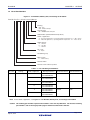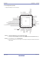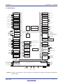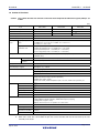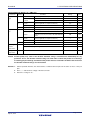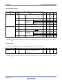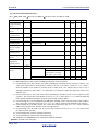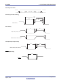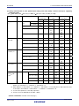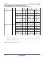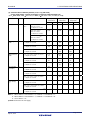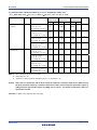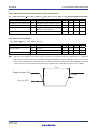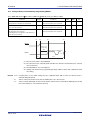
1
Datasheet RL78/G1D R01DS0258EJ0100 Rev.1.00 Apr 24, 2015 RENESAS MCU 1. OUTLINE The RL78/G1D is a microcomputer incorporating the RL78 CPU core and low power consumption RF transceiver supporting the Bluetooth ver.4.1 (Low Energy Single mode) specifications. 1.1 Features Ultra-low power consumption technology MCU part Standby function HALT mode, STOP mode, SNOOZE mode RF part POWER_DOWN mode, RESET_RF mode, STANDBY_RF mode, IDLE_RF mode, Standby function DEEP_SLEEP mode, SLEEP_RF mode RF transmission RF reception (RF normal mode) : 4.3 mA (TYP.) (3.0 V/MCU part: STOP mode) (RF Low power mode) : 2.6 mA (TYP.) (3.0 V/MCU part: STOP mode) (RF normal mode) : 3.5 mA (TYP.) (3.0 V/MCU part: STOP mode) (RF Low power mode) RF sleep (POWER_DOWN mode) operation : 3.3 mA (TYP.) (3.0 V/MCU part: STOP mode) : 0.10 A (TYP.) (3.0 V/MCU part: STOP mode) RL78 CPU core CISC architecture with 3-stage pipeline Minimum instruction execution time: Can be changed from high speed (0.03125 s: @ 32 MHz operation with highspeed on-chip oscillator) to ultra-low speed (30.5 s: @ 32.768 kHz operation with subsystem clock) Address space: 1 MB General-purpose registers: (8-bit register × 8) × 4 banks On-chip RAM: 12 to 20 KB On-chip RF transceiver Bluetooth v4.1 Specification (Low Energy Single mode) 2.4 GHz ISM band, GFSK modulation, TDMA/TDD frequency hopping (including AES encryption circuit) Adaptivity, exclusively for use in operation as a slave device Code flash memory Code flash memory: 128 to 256 KB Block size: 1 KB Prohibition of block erase and rewriting (security function) On-chip debug function Self-programming (with boot swap function/flash shield window function) Data flash memory Data flash memory: 8 KB Back ground operation (BGO): Instructions can be executed from the program memory while rewriting the data flash memory. Number of rewrites: 1,000,000 times (TYP.) Voltage of rewrites: VDD = 1.8 to 3.6 V R01DS0258EJ0100 Rev.1.00 Apr 24, 2015 Page 1 of 74 RL78/G1D CHAPTER 1 OUTLINE High-speed on-chip oscillator Select from 32 MHz (TYP.), 24 MHz (TYP.), 16 MHz (TYP.), 12 MHz (TYP.), 8 MHz (TYP.), 6 MHz (TYP.), 4 MHz (TYP.), 3 MHz (TYP.), 2 MHz (TYP.), and 1 MHz (TYP.) Low-speed on-chip oscillator 15 kHz (TYP.) On-chip oscillator for the RF slow clock 32.768 kHz (TYP.) Operating ambient temperature TA = 40 to +85°C (A: Consumer applications, D: Industrial applications) Power management and reset function On-chip power-on-reset (POR) circuit On-chip voltage detector (LVD) (Select interrupt and reset from 12 levels) DMA (Direct Memory Access) controller 4 channels Number of clocks during transfer between 8/16-bit SFR and internal RAM: 2 clocks Multiplier and divider/multiply-accumulator 16 bits × 16 bits = 32 bits (Unsigned or signed) 32 bits ÷ 32 bits = 32 bits (Unsigned) 16 bits × 16 bits + 32 bits = 32 bits (Unsigned or signed) Serial interface CSI: 2 channels UART: 2 channels I C/Simplified I C: 2 2 3 channels Timer 16-bit timer: 8 channels 12-bit interval timer: 1 channel Real-time clock: 1 channel (calendar for 99 years, alarm function, and clock correction function) Watchdog timer: 1 channel (operable with the dedicated low-speed on-chip oscillator) A/D converter 8/10-bit resolution A/D converter (VDD = 1.6 to 3.6 V) Analog input: 8 channels Internal reference voltage (1.45 V) and temperature sensorNote I/O port I/O port: 32 Can be set to N-ch open drain, TTL input buffer, and on-chip pull-up resistor Different potential interface: Can connect to a 1.8/2.5 V device On-chip clock output/buzzer output controller R01DS0258EJ0100 Rev.1.00 Apr 24, 2015 Page 2 of 74 RL78/G1D CHAPTER 1 OUTLINE Others On-chip BCD (binary-coded decimal) correction circuit Note Can be selected only in HS (high-speed main) mode ROM, RAM capacities Flash ROM Data Flash RAM RL78/G1D 128 KB 8 KB 12 KB R5F11AGG 192 KB 8 KB 16 KB R5F11AGH 256 KB 8 KB 20 KB Note R5F11AGJ Note 19 KB when the self-programming function is used. R01DS0258EJ0100 Rev.1.00 Apr 24, 2015 Page 3 of 74 RL78/G1D CHAPTER 1 OUTLINE 1.2 List of Part Numbers Figure 1-1. Part Number, Memory Size, and Package of RL78/G1D Part No. R 5 F 1 1 A G G A x x x N B # 20 Packing #20 : Tray #40 : Embossed Tape Package type: NB : HWQFN, 0.40 mm pitch ROM number (Omitted with blank products) Fields of application: A : Consumer applications, operating ambient temperature :TA = −40 to +85 °C D : Industrial applications, operating ambient temperature : TA = −40 to +85 °C ROM capacity: G : 128 KB H : 192 KB J : 256 KB Pin count: G : 48-pin RL78/G1D group Memory type: F : Flash memory Renesas MCU Renesas semiconductor product Table 1-1. List of Ordering Part Numbers Pin count 48 pins Package Plastic WQFN (6 6) Fields of Application A Note Ordering Part Number R5F11AGGANB#20 Code Flash Memory Data Flash Memory 128 KB 8 KB 192 KB 8 KB 256 KB 8 KB R5F11AGGANB#40 D R5F11AGGDNB#20 R5F11AGGDNB#40 A R5F11AGHANB#20 R5F11AGHANB#40 D R5F11AGHDNB#20 R5F11AGHDNB#40 A R5F11AGJANB#20 R5F11AGJANB#40 D R5F11AGJDNB#20 R5F11AGJDNB#40 Note For the fields of application, see Figure 1-1 Part Number, Memory Size, and Package of RL78/G1D. Caution The ordering part numbers represent the numbers at the time of publication. For the latest ordering part numbers, refer to the target product page of the Renesas Electronics website. R01DS0258EJ0100 Rev.1.00 Apr 24, 2015 Page 4 of 74 RL78/G1D CHAPTER 1 OUTLINE 1.3 Pin Configuration (Top View) GND1 2 3 4 5 6 24 23 22 21 20 19 18 17 16 15 14 13 7 8 9 10 11 12 P61/SDDA0 P60/SCLA0 V DD V SS REGC P121/X1 P122/X2/EXCLK P137/INTP0 P123/XT1 P124/XT2/EXCLKS RESET P40/TOOL0 P02/ANI17/TxD1 P01/TO00 P00/TI00 P140/PCLBUZ0/INTP6 P120/ANI19 1 exposed die pad P20/ANI0/AVREFP P130 P03/ANI16/RxD1 INDEX MARK 36 35 34 33 32 31 30 29 28 27 26 25 37 38 39 40 41 42 43 44 45 46 47 48 P147/ANI18 P23/ANI3 P22/ANI2 P21/ANI1/AVREFM V SS_RF DCLIN GPIO2/CLKOUT_RF GPIO3/EXSLK_RF P30/INTP3/RTC1HZ P16/TI01/TO01/INTP5 P15/SCK20/SCL20/(TI02)/(TO02) P14/SI20/SDA20/(SCLA0)/(TI03)/(TO03) P13/SO20/(SDAA0)/(TI04)/(TO04) P12/SO00/TxD0/TOOLTxD/(TI05)/(TO05) P11/SI00/RxD0/TOOLRxD/SDA00/(TI06)/(TO06) P10/SCK00/SCL00/(TI07)/(TO07) IC0 IC1 RFCTLEN GPIO0/TXSELH_RF GPIO1/TXSELL_RF DCLOUT V DD_RF AV DD_RF XTAL1_RF XTAL2_RF AV SS_RF ANT 48-pin plastic WQFN (6 6 mm, 0.4 mm pitch) Cautions 1. Connect the REGC pin to Vss via a capacitor (0.47 to 1 F). 2. Connect the metal pad (GND1) on the back of the package that has the same potential as AVSS_RF. Remarks 1. For pin identification, see 1.4 Pin Identification. 2. Functions in parentheses in the above figure can be assigned via settings in the peripheral I/O redirection register (PIOR). R01DS0258EJ0100 Rev.1.00 Apr 24, 2015 Page 5 of 74 RL78/G1D CHAPTER 1 OUTLINE 1.4 Pin Identification Analog input PCLBUZ0: Programmable clock output/buzzer ANT: Antenna connection REGC: Regulator capacitance AVDD_RF: Power supply for RF RFCTLEN: RF control enable analog RTC1HZ: Real-time clock correction clock minus RESET: Reset ANI0 to ANI3, output ANI16 to ANI19: AVREFM: (1 Hz) output Analog reference voltage Analog reference voltage RxD0, RxD1: Receive data plus SCLA0: Serial clock input/output AVSS_RF: Ground for RF analog SCK00, SCK20, Serial clock output CLKOUT_RF: Clock output SCL00, SCL20: AVREFP: DCLIN: DC-DC converter inductor SDAA0, SDA00, SDA20: Serial data input/output and DCLOUT capacitor SI00, SI20: Serial data input DCLOUT: DC-DC converter output SO00, SO20: Serial data output EXCLK: External clock input TI00 to TI07: Timer input (Main system clock) TO00 to TO07: Timer output External clock input TOOL0: Data input/output for tool EXCLKS: (Subsystem clock) TOOLRxD, TOOLTxD: Data input/output for external device EXSLK_RF: External slow clock input TxD0, TxD1: Transmit data GND1: Package exposed die pad TXSELL_RF, GPIO0 to GPIO3: GPIO at RF unit TXSELH_RF: IC0, IC1: Internal circuit VDD: Power supply INTP0, INTP3, External interrupt input VDD_RF: Power Supply for RF INTP5, INTP6: External PA/LNA control VSS: Ground P00 to P03: Port 0 VSS_RF: Ground for RF P10 to P16: Port 1 X1, X2: Crystal oscillator (Main system clock) P20 to P23: Port 2 XT1, XT2: Crystal oscillator (Subsystem clock) P30: Port 3 XTAL1_RF, Crystal oscillator (RF clock) P40: Port 4 XTAL2_RF: P60, P61: Port 6 P120 to P124: Port 12 P130, P137: Port 13 P140, P147: Port 14 R01DS0258EJ0100 Rev.1.00 Apr 24, 2015 Page 6 of 74 RL78/G1D CHAPTER 1 OUTLINE 1.5 Block Diagram TIMER ARRAY UNIT (8ch) PORT 0 4 P00 to P03 TI00/P00 TO00/P01 ch0 PORT 1 7 P10 to P16 TI01/TO01/P16 ch1 PORT 2 4 P20 to P23 (TI02/TO02/P15) ch2 (TI03/TO03/P14) ch3 (TI04/TO04/P13) ch4 (TI05/TO05/P12) ch5 (TI06/TO06/P11) ch6 (TI07/TO07/P10) ch7 RTC1HZ/P30 PORT 4 P40 RL78 CPU CORE CODE FLASH MEMORY PORT 12 DATA FLASH MEMORY PORT 14 REAL-TIME CLOCK UART0 RxD1/P03 TxD1/P02 UART1 P60, P61 4 P120 P121 to P124 P130 P137 PORT 13 12- BIT INTERVAL TIMER RxD0/P11 TxD0/P12 2 PORT 7 A/D CONVERTER RAM 2 P140, P147 4 ANI0/P20 to ANI3/P23 4 ANI16/P03, ANI17/P02, ANI18/P147, ANI19/P120 AVREFP/P20 AVREFM/P21 SERIAL ARRAY UNIT0 (4ch) SCK00/P10 SI00/P11 SO00/P12 SCL00/P10 P30 PORT 6 WINDOW WATCHDOG TIMER LOW-SPEED ON-CHIP OSCILLATOR PORT 3 POWER ON RESET/VOLTAGE DETECTOR SERIAL INTERFACE IICA0 POR/LVD CONTROL SCLA0/P60(SCLA0/P14) SDAA0/P61(SDAA0/P13) RESET CONTROL CSI00 BUZZER OUTPUT TOOL0/P40 CLOCK OUTPUTCONTROL SYSTEM CONTROL MULTIPLIER& DIVIDER, MULITIPLYACCUMULATOR SERIAL ARRAY UNIT1 (2ch) SCK20/P15 SI20/P14 SO20/P13 SCL20/P15 SDA20/P14 ON-CHIP DEBUG PCLBUZ0/P140 IIC00 SDA00/P11 CSI20 CRC HIGH-SPEED ON-CHIP DIRECT MEMORY ACCESS CONTROL IIC20 OSCILLATOR XT1/P123 XT2/EXCLKS/P124 VOLTAGE REGULATOR REGC BCD ADJUSTMENT CSI21 RESET X1/P121 X2/EXCLK/P122 INTERRUPT CONTROL INTP0/P137 INTP3/P30 INTP5/P16 INTP6/P140 SCK21/P70 SO21/P72 SI21/P71 GPIO0/TXSELH_RF GPIO1/TXSELL_RF GPIO2/CLKOUT_RF GPIO3/EXSLK_RF ANT P05 P06 SPI 32.768 kHz ON-CHIP OSCILLATOR INT_RF P74 CONTROL RFCTLEN XTAL1_RF XTAL2_RF DCLIN DCLOUT RF TRANSCEIVER (RF Unit) 2 TOOLRxD/P11, TOOLTxD/P12 Remark VDD VDD_RF AVDD_RF VSS VSS_RF AVSS_RF IC0, IC1 GND1 Functions in parentheses in the above figure can be assigned via settings in the peripheral I/O redirection register (PIOR). R01DS0258EJ0100 Rev.1.00 Apr 24, 2015 Page 7 of 74 RL78/G1D CHAPTER 1 OUTLINE 1.6 Outline of Functions Caution This outline describes the functions at the time when Peripheral I/O redirection register (PIOR) is set to 00H. (1/2) Item R5F11AGG R5F11AGH R5F11AGJ Code flash memory 128 KB 192 KB 256 KB Data flash memory 8 KB 8 KB 8 KB RAM 12 KB 16 KB 20 KB Address space 1 MB System clock (RF side) 32 MHz Main system clock High-speed system clock External main system clock input (EXCLK) 1 to 20 MHz: VDD = 2.7 to 3.6 V, 1 to 8 MHz: VDD = 1.8 to 2.7 V, 1 to 4 MHz: VDD = 1.6 to 1.8 V High-speed on-chip oscillation clock HS (High-speed main) mode: 1 to 32 MHz (VDD = 2.7 to 3.6 V), HS (High-speed main) mode: 1 to 16 MHz (VDD = 2.4 to 3.6 V), LS (Low-speed main) mode: 1 to 8 MHz (VDD = 1.8 to 3.6 V), LV (Low-voltage main) mode: 1 to 4 MHz (VDD = 1.6 to 3.6 V) Subsystem clock RF slow clock Note 1 XT1 (Crystal) oscillation, External main system clock input (EXCLKS) 32.768 kHz (TYP.) External input External clock input for RF block (EXSLK_RF) 32.768 kHz (TYP.) On-chip Oscillator 32.768 kHz (TYP.) Low-speed on-chip oscillator 15 kHz (TYP.) General-purpose register (8-bit register 8) 4 banks Minimum instruction execution time 0.03125 s (High-speed on-chip oscillation clock: fIH = 32 MHz operation) 0.05 s (High-speed system clock: fMX = 20 MHz operation) 30.5 s (Subsystem clock: fSUB = 32.768 kHz operation) Instruction set I/O port Data transfer (8/16 bits) Adder and subtractor/logical operation (8/16 bits) Multiplication (8 bits 8 bits) Rotate, barrel shift, and bit manipulation (Set, reset, test, and Boolean operation), etc. Note 2 Total 32 CMOS I/O 20 Note 2 Note 2 CMOS input 5 CMOS output 1 Note 2 N-ch O.D. I/O 2 GPIO (RF block) 4 2.4 GHz RF transceiver Supporting Bluetooth v4.1 Specification (Single mode). 2.4 GHz ISM Band, GFSK modulation, TDMA/TDD frequency hopping (Including AES encryption circuit.) Adaptivity, exclusively for use in operation as a slave device Timer Notes 1. 2. 16-bit timer 8 channels Watchdog timer 1 channel Real-time clock (RTC) 1 channel 12-bit interval timer 1 channel This is about 19 KB when the self-programming function is used. When RF is used, this count includes the pins that connect the MCU with the RF transceiver by the user externally on the board. R01DS0258EJ0100 Rev.1.00 Apr 24, 2015 Page 8 of 74 RL78/G1D CHAPTER 1 OUTLINE (2/2) R5F11AGG Item Timer R5F11AGH Timer output 8 channels (PWM outputs: 3 RTC output 1 channel R5F11AGJ Note 1 Note 2 ) 1 Hz (subsystem clock: fSUB = 32.768 kHz) Clock output/buzzer output Note 1 1 2.44 kHz, 4.88 kHz, 9.76 kHz, 1.25 MHz, 2.5 MHz, 5 MHz, 10 MHz (Main system clock: fMAIN = 20 MHz operation) 256 Hz, 512 Hz, 1.024 kHz, 2.048 kHz, 4.096 kHz, 8.192 kHz, 16.384 kHz, 32.768 kHz (Subsystem clock: fSUB = 32.768 kHz operation) RF unit CLKOUT_RF pin : 16 MHz, 8 MHz, 4 MHz 8/10-bit resolution A/D converter 8 channels Serial interface CSI/simplified I C/UART: 1 channel 2 2 CSI/simplified I C: 1 channel UART: 1 channel CSI: 1 channel (dedicated for internal communications) 2 I C bus 1 channel Multiplier and divider/multiply- Multiplication: 16 bits 16 bits = 32 bits (Unsigned or signed) accumulator Division: 32 bits 32 bits = 32 bits (Unsigned) Multiply-accumulate: 16 bits 16 bits + 32 bits = 32 bits (Unsigned or signed) DMA controller 4 channels Vectored interrupt Internal 29 sources External 4 Note 3 Reset by RESET pin Reset Internal reset by watchdog timer Internal reset by power-on-reset Internal reset by voltage detector Internal reset by illegal instruction execution Note 4 Internal reset by RAM parity error Internal reset by illegal-memory access Power-on-reset circuit Power-on-reset: 1.51 (TYP.) Power-down-reset: 1.50 (TYP.) Voltage detector Rising edge : 1.67 V to 3.13 V (12 stages) Falling edge : 1.63 V to 3.06 V (12 stages) On-chip debug function Provided Power supply voltage range VDD = 1.6 to 3.6 V (VDD =1.8 to 3.6 V on usage of DC-DC converter) Operating ambient temperature TA = 40 to +85 C Package 48-pin QFN (6 6), (0.4 mm pitch) Notes 1. The number of outputs varies, depending on the setting of channels in use and the number of the master 2. When setting to PIOR0 = 1 3. When RF is used, this count includes the pins that connect the MCU with the RF transceiver by the user externally on the board. 4. The illegal instruction is generated when instruction code FFH is executed. Reset by the illegal instruction execution not issued by emulation with the on-chip debug emulator. R01DS0258EJ0100 Rev.1.00 Apr 24, 2015 Page 9 of 74 RL78/G1D 2. ELECTRICAL SPECIFICATIONS 2. ELECTRICAL SPECIFICATIONS Caution The RL78 microcontrollers have an on-chip debug function, which is provided for development and evaluation. Do not use the on-chip debug function in products designated for mass production, because the guaranteed number of rewritable times of the flash memory may be exceeded when this function is used, and product reliability therefore cannot be guaranteed. Renesas Electronics is not liable for problems occurring when the on-chip debug function is used. R01DS0258EJ0100 Rev.1.00 Apr 24, 2015 Page 10 of 74 RL78/G1D 2. ELECTRICAL SPECIFICATIONS 2.1 Absolute Maximum Ratings Absolute Maximum Ratings (TA = 25C) (1/2) Parameter Symbols Supply voltage Input voltage Conditions Ratings Unit VDD VDD 0.5 to +6.5 V VDDRF1 VDD_RF 0.5 to +4.0 V VDDRF2 AVDD_RF 0.5 to +4.0 V VDDRF3 DCLIN 0.5 to +4.0 V VSSRF VSS_RF, AVSS_RF 0.5 to +0.3 VI1 0.3 to VDD+0.3 P00, P01, P02, P03, P10, P11, P12, P14, P15, P16, P20, V Note 1 V P21, P22, P23, P30, P40, P120, P121, P122, P123, P124, P137, P140, P147, RESET VI2 Output voltage VIRF1 GPIO0, GPIO1, GPIO2, GPIO3 VIRF2 ANT VO 0.3 to +6.5 P60, P61 V 0.3 to VDD_RF+0.3 Note 2 0.5 to +1.4 0.3 to VDD+0.3 P00, P01, P02, P03, P10, P11, P12, P14, P15, P16, P20, V V Note 1 V P21, P22, P23, P30, P40, P60, P61, P120, P130, P140, P147 Analog input VORF GPIO0, GPIO1, GPIO2, GPIO3, DCLOUT VAI ANI0, ANI1, ANI2, ANI3, ANI16, ANI17, ANI18, ANI19 0.3 to VDD_RF+0.3 0.3 to VDD+0.3 and 0.3 to VREF(+)+0.3 voltage REGC pin input VIREGC REGC IC pin input VIIC IC0, IC1 0.5 to +0.3 V V Notes 2, 4 0.3 to +2.8 and 0.3 to VDD+0.3 voltage Note 2 V Note 3 V voltage Notes 1. Must be 6.5 V or lower. 2. Must be 4.0 V or lower. 3. Connect the REGC pin to Vss via a capacitor (0.47 to 1 μF). This value regulates the absolute maximum rating of the REGC pin. Do not use this pin with voltage applied to it. 4. Do not exceed AVREF(+) + 0.3 V in case of A/D conversion target pin. Caution Product quality may suffer if the absolute maximum rating is exceeded even momentarily for any parameter. That is, the absolute maximum ratings are rated values at which the product is on the verge of suffering physical damage, and therefore the product must be used under conditions that ensure that the absolute maximum ratings are not exceeded. Remarks 1. Unless specified otherwise, the characteristics of alternate-function pins are the same as those of the port pins. 2. AVREF (+) : + side reference voltage of the A/D converter. 3. Reference voltage is V SS . R01DS0258EJ0100 Rev.1.00 Apr 24, 2015 Page 11 of 74 RL78/G1D 2. ELECTRICAL SPECIFICATIONS Absolute Maximum Ratings (TA = 25C) (2/2) Parameter Symbols Output current, IOH1 high IOH2 Conditions Ratings Unit Per pin (This is applicable to all pins listed below.) 40 mA Total of all pins P00, P01, P02, P03, P40, P120, P130, P140 70 mA 170mA P10, P11, P12, P13, P14, P15, P16, P30, P147 100 mA Per pin (This is applicable to all pins listed below.) 0.5 mA Total of all pins P20, P21, P22, P23 2 mA Per pin GPIO0, GPIO1, GPIO2, GPIO3 17 mA Output current, IOL1 Per pin (This is applicable to all pins listed below.) 40 mA low Total of all pins P00, P01, P02, P03, P40, P120, P130, P140 70 mA 170mA P10, P11, P12, P13, P14, P15, P16, P30, P60, P61, 100 mA IOHMRF P147 IOL2 Operating Per pin (This is applicable to all pins listed below.) 1 mA Total of all pins P20, P21, P22, P23 5 mA IOLRF Per pin GPIO0, GPIO1, GPIO2, GPIO3 17 mA TA In normal operation mode 40 to +85 °C In flash memory programming mode 40 to +85 °C 65 to +150 °C ambient temperature Storage Tstg temperature Caution Product quality may suffer if the absolute maximum rating is exceeded even momentarily for any parameter. That is, the absolute maximum ratings are rated values at which the product is on the verge of suffering physical damage, and therefore the product must be used under conditions that ensure that the absolute maximum ratings are not exceeded. Remarks 1. Unless specified otherwise, the characteristics of alternate-function pins are the same as those of the port pins. 2. AVREF (+) : + side reference voltage of the A/D converter. 3. Reference voltage is V SS . R01DS0258EJ0100 Rev.1.00 Apr 24, 2015 Page 12 of 74 RL78/G1D 2. ELECTRICAL SPECIFICATIONS 2.2 Operating Voltage (TA = 40 to +85°C, VDD = VDD_RF = AVDD _RF, VSS = VSS_RF = AVSS_RF = 0 V) Clock generator Flash operation mode Operation voltage CPU operation clocks Note 1 (fCLK) Main system clock (fMAIN) High-speed on-chip oscillator HS (high-speed main) mode (fIH) LS (low-speed main) mode Note 2 LV (low-voltage main) mode X1 clock oscillator (fX) HS (high-speed main) mode LS (low-speed main) mode Note 2 LV (low-voltage main) mode External main system clock HS (high-speed main) mode (fEX) LS (low-speed main) mode LV (low-voltage main) mode Note 2 2.7 V VDD 3.6 V 1 MHz to 32 MHz 2.4 V VDD < 2.7 V 1 MHz to 16 MHz 1.8 V VDD 3.6 V 1 MHz to 8 MHz 1.6 V VDD 3.6 V 1 MHz to 4 MHz 2.7 V VDD 3.6 V 1 MHz to 20 MHz 1.8 V VDD 3.6 V 1 MHz to 8 MHz 1.6 V VDD 3.6 V 1 MHz to 4 MHz 2.7 V VDD 3.6 V 1 MHz to 20 MHz 2.4 V VDD < 2.7 V 1 MHz to 16 MHz 1.8 V VDD 3.6 V 1 MHz to 8 MHz 1.6 V VDD 3.6 V 1 MHz to 4 MHz Subsystem clock XT1 clock oscillator (fXT) 1.6 V VDD 3.6 V 32.768 kHz (fSUB) External subsystem clock 1.6 V VDD 3.6 V 32.768 kHz (fEXT) Notes 1. Indicates only permissible oscillator frequency ranges. Refer to AC Characteristics for instruction execution time.Request evaluation by the manufacturer of the oscillator circuit mounted on a board to check the oscillator characteristics. 2. This mode is prohibited to use in case of using DC-DC converter. R01DS0258EJ0100 Rev.1.00 Apr 24, 2015 Page 13 of 74 RL78/G1D 2. ELECTRICAL SPECIFICATIONS 2.3 Oscillator Characteristics 2.3.1 X1, XT1, XRF oscillator characteristics (TA = 40 to +85°C, 1.6 V VDD = VDD_RF = AVDD_RF 3.6 V, VSS = VSS_RF = AVSS_RF = 0 V) Parameter X1 clock oscillation frequency Note 1 Symbol Ceramic resonator fX Crystal resonator Conditions MIN. Note 1 RF base clock oscillation frequency RF base clock oscillation frequency accuracy Unit 1 20 MHz 1.8 V VDD < 2.7 V 1 8 MHz 4 MHz 35 kHz 1 fXT Note 2 MAX. 2.7 V VDD 3.6 V 1.6 V VDD 1.8 V XT1 clock oscillation frequency TYP. 32 fXRF 32.768 32 fXRFP -20 MHz +20 ppm Note 2 Notes 1. Indicates only permissible oscillator frequency ranges. Refer to AC Characteristics for instruction execution time. Request evaluation by the manufacturer of the oscillator circuit mounted on a board to check the oscillator characteristics. 2. This Oscillator characteristics is base clock for RF Transceiver. Caution Since the CPU is started by the high-speed on-chip oscillator clock after a reset release, check the X1 clock oscillation stabilization time using the oscillation stabilization time counter status register (OSTC) by the user. Determine the oscillation stabilization time of the OSTC register and the oscillation stabilization time select register (OSTS) after sufficiently evaluating the oscillation stabilization time with the resonator to be used. 2.3.2 On-chip oscillator characteristics (TA = 40 to +85°C, 1.6 V VDD = VDD_RF = AVDD_RF 3.6 V, VSS = VSS_RF = AVSS_RF = 0 V) Oscillators High-speed on-chip oscillator clock frequency Symbol MAX. Unit 1 32 MHz 20 to +85C -1.5 1.5. % 40 to 20C -2.5 2.5. % fIH MIN. TYP. Notes 1, 2 High-speed on-chip oscillator clock fIHP frequency accuracy Low-speed on-chip oscillator clock frequency Conditions 15 fIL kHz Notes 3 Low-speed on-chip oscillator clock fILP 15 +15 % frequency accuracy On-chip oscillator clock frequency for the fILRF 32.768 kHz Note 3 RF slow clock On-chip oscillator clock frequency accuracy fILRFP -0.025 0.025 % for the RF slow clock Notes 1. High-speed on-chip oscillator frequency is selected by bits 0 to 3 of option byte (000C2H/010C2H) and bits 0 to 2 of HOCODIV register. 2. This indicates the oscillator characteristics only. Refer to AC Characteristics for instruction execution time. 3. This indicates the oscillator characteristics only. R01DS0258EJ0100 Rev.1.00 Apr 24, 2015 Page 14 of 74 RL78/G1D 2. ELECTRICAL SPECIFICATIONS 2.4 DC Characteristics 2.4.1 Output current (TA = 40 to +85°C, 1.6 V VDD = VDD_RF = AVDD_RF 3.6 V, VSS = VSS_RF = AVSS_RF = 0 V) Items Output current, high Symbol IOH1 Note 1 Conditions P00, P01, P02, P03, P10, P11, P12, MIN. TYP. Per pin 1.6 V VDD 3.6 V MAX. 10.0 Note 2 Unit mA P13, P14, P15, P16, P30, P40, P120, P130, P140, P147 P00, P01, P02, P03, P40, P120, P130, Total Note 3 2.7 V VDD 3.6 V 10.0 mA P140 1.8 V VDD < 2.7 V 5.0 mA 1.6 V VDD < 1.8 V 2.5 mA P10, P11, P12, P13, P14, P15, P16, Total Note 3 P30, P147 Note 3 Total of all pins IOH2 P20, P21, P22, P23 Per pin Output current, IOL1 Note 1 low GPIO0, GPIO1, GPIO2, GPIO3 P00, P01, P02, P03, P10, P11, P12, 19.0 mA 1.8 V VDD < 2.7 V 10.0 mA 1.6 V VDD < 1.8 V 5.0 mA 1.6 V VDD 3.6 V 135.0 mA 1.6 V VDD 3.6 V 0.1 Note 4 Note 2 mA 1.6 V VDD 3.6 V 1.5 mA Per pin 1.6 V VDD_RF 3.6 V 2.0 mA Per pin 1.6 V VDD 3.6 V Per pin 1.6 V VDD 3.6 V Total IOHRF 2.7 V VDD 3.6 V Note 3 20.0 Note 2 mA 15.0 Note 2 mA P13, P14, P15, P16, P30, P40, P120, P130, P140, P147 P60, P61 P00, P01, P02, P03, P40, P120, P130, Total P140 Note 3 P10, P11, P12, P13, P14, P15, P16, Note 3 1.8 V VDD < 2.7 V 9.0 mA 1.6 V VDD < 1.8 V 4.5 mA 35.0 mA 20.0 mA 1.6 V VDD < 1.8 V 10.0 mA Total of all pins 1.6 V VDD 3.6 V 150.0 mA P20, P21, P22, P23 1.6 V VDD 3.6 V Per pin Total Notes 1. mA 1.8 V VDD < 2.7 V Note 3 IOLRF 15.0 2.7 V VDD 3.6 V Total P30, P60, P61, P147 IOL2 2.7 V VDD 3.6 V GPIO0, GPIO1, GPIO2, GPIO3 Note 3 Per pin 0.4 Note 2 mA 1.6 V VDD 3.6 V 5.0 mA 1.6 V VDD_RF 3.6 V 2.0 mA Value of current at which the device operation is guaranteed even if the current flows from the VDD pin to an output pin. 2. 3. However, do not exceed the total current value. Specification under conditions where the duty factor 70%. The output current value that has changed to the duty factor > 70% the duty ratio can be calculated with the following expression (when changing the duty factor from 70% to n%). Total output current of pins = (IOH × 0.7)/(n × 0.01) <Example> Where n = 50% and IOH = 10.0 mA Total output current of pins = (10.0 × 0.7)/(50 × 0.01) = 14.0 mA However, the current that is allowed to flow into one pin does not vary depending on the duty factor. A current higher than the absolute maximum rating must not flow into one pin. 4. Product for industrial applications (R5F11AGGDNB, R5F11AGHDNB, R5F11AGJDNB) is 100.0 mA. (Caution and Remark are listed on the next page.) R01DS0258EJ0100 Rev.1.00 Apr 24, 2015 Page 15 of 74 RL78/G1D 2. ELECTRICAL SPECIFICATIONS Caution P00, P02, P03, and P10 to P15 do not output high level in N-ch open-drain mode. Remark Unless specified otherwise, the characteristics of alternate-function pins are the same as those of the port pins. 2.4.2 Input current (TA = 40 to +85°C, 1.6 V VDD = VDD_RF = AVDD_RF 3.6 V, VSS = VSS_RF = AVSS_RF = 0 V) Items Symbol Input voltage, high VIH1 Conditions P00, P01, P02, P03, P10, P11, Normal mode (ITHL = 1) MIN. TYP. MAX. Unit 0.8VDD VDD V 2.0 VDD V 1.5 VDD V P12, P13, P14, P15, P16, P30, P40, P120, P130, P140, P147 VIH2 P01, P03, P10, P11, P13, P14, TTL mode P15, P16 3.3 V VDD 3.6 V TTL mode 1.6 V VDD < 3.3V Input voltage, low VIH3 P20, P21, P22, P23 0.7VDD VDD V VIH4 P60, P61 0.7VDD 6.0 V VIH5 P121, P122, P123, P124, P137, RESET 0.8VDD VDD V VIHRF GPIO0, GPIO1, GPIO2, GPIO3 0.85VDD_RF VDD_RF V VIL1 P00, P01, P02, P03, P10, P11, Normal mode (ITHL = 1) 0 0.2VDD V P01, P03, P10, P11, P13, P14, TTL mode 0 0.5 V P15, P16 3.3 V VDD 3.6 V 0 0.32 V P12, P13, P14, P15, P16, P30, P40, P120, P140, P147 VIL2 TTL mode 1.6 V VDD < 3.3V VIL3 P20, P21, P22, P23 0 0.3VDD V VIL4 P60, P61 0 0.3VDD V VIL5 P121, P122, P123, P124, P137, RESET 0 0.2VDD V VILRF GPIO0, GPIO1, GPIO2, GPIO3 0 0.1VDD_RF V Caution The maximum value of VIH of pins P00, P02, P03, and P10 to P15 is VDD, even in the N-ch open-drain mode. Remark Unless specified otherwise, the characteristics of alternate-function pins are the same as those of the port pins. R01DS0258EJ0100 Rev.1.00 Apr 24, 2015 Page 16 of 74 RL78/G1D 2. ELECTRICAL SPECIFICATIONS 2.4.3 Output voltage (TA = 40 to +85°C, 1.6 V VDD = VDD_RF = AVDD_RF 3.6 V, VSS = VSS_RF = AVSS_RF = 0 V) Items Output Symbol VOH1 voltage, high Output Conditions MIN. TYP. MAX. Unit IOH = 2.0 mA P00, P01, P02, P03, P10, 2.7 V VDD 3.6 V VDD 0.6 V IOH = 1.5 mA P11, P12, P13, P14, P15, 1.8 V VDD 3.6 V VDD 0.5 V 1.6 V VDD 3.6 V VDD 0.5 V IOH = 1.0 mA P16, P30, P40, P120, P140, P147 IOH = 10 A P130 VDD 0.3 V VOH2 IOH = 100 A P20, P21, P22, P23 VDD 0.5 V VOHRF IOH = 2.0 mA GPIO0, GPIO1, GPIO2, 2.7 V VDD_RF 3.6 V VDD_RF 0.3 V IOH = 1.5 mA GPIO3 1.8 V VDD_RF 3.6 V VDD_RF 0.3 V IOL = 3.0 mA P00, P01, P02, P03, P10, 2.7 V VDD 3.6 V IOL = 1.5 mA P11, P12, P13, P14, P15, VOL1 voltage, low IOL = 0.6 mA 0.6 V 0.4 V 1.8 V VDD 3.6 V 0.4 V 1.6 V VDD 3.6 V 0.4 V P20, P21, P22, P23 0.4 V GPIO0, GPIO1, GPIO2, GPIO3 0.3 V P16, P30, P40, P120, P130, P140, P147 IOL = 0.3 mA VOL2 IOL = 400 A VOLRF Caution P00, P02, P03, and P10 to P15 do not output high level in N-ch open-drain mode. Remark Unless specified otherwise, the characteristics of alternate-function pins are the same as those of the port pins. R01DS0258EJ0100 Rev.1.00 Apr 24, 2015 Page 17 of 74 RL78/G1D 2. ELECTRICAL SPECIFICATIONS 2.4.4 Input leakage current (TA = 40 to +85°C, 1.6 V VDD = VDD_RF = AVDD_RF 3.6 V, VSS = VSS_RF = AVSS_RF = 0 V) Items Symbol Input leakage current, ILIH1 Conditions VI = VDD MIN. TYP. P00, P01, P02, P03, P10, P11, P12, P13, P14, MAX. Unit 1 A P15, P16, P30, P40, P60, P61, P120, P140, high P147 ILIH2 VI = VDD P20, P21, P22, P23, P137, RESET 1 A ILIH3 VI = VDD P121, P122, P123, In input port 1 A P124 (EXCLK, In external clock input 1 A In resonator connection 10 A EXCLKS) (XT1, XT2) Input leakage current, ILIHRF VI = VDD_RF GPIO0, GPIO1, GPIO2, GPIO3 10 A ILIL1 VI = VSS P00, P01, P02, P03, P10, P11, P12, P13, P14, -1 A P15, P16, P30, P40, P60, P61, P120, P140, low P147 ILIL2 VI = VSS P20, P21, P22, P23, P137, RESET -1 A ILIL3 VI = VSS P121, P122, P123, In input port -1 A P124 (EXCLK, In external clock input -1 A In resonator connection -10 A -10 A EXCLKS) (XT1, XT2) ILILRF Remark VI = VSS_RF GPIO0, GPIO1, GPIO2, GPIO3 Unless specified otherwise, the characteristics of alternate-function pins are the same as those of the port pins. 2.4.5 Resistance (TA = 40 to +85°C, 1.6 V VDD = VDD_RF = AVDD_RF 3.6 V, VSS = VSS_RF = AVSS_RF = 0 V) Items Symbol On-chip pll-up RU Conditions VI = VSS P00, P01, P02, P03, P10, P11, P12, P13, P14, MIN. TYP. MAX. Unit 10 20 100 k P15, P16, P30, P40, P120, P140, P147 resistance In input mode Remark Unless specified otherwise, the characteristics of alternate-function pins are the same as those of the port pins. R01DS0258EJ0100 Rev.1.00 Apr 24, 2015 Page 18 of 74 RL78/G1D 2. ELECTRICAL SPECIFICATIONS 2.5 Current Drawn The current drawn by the RL78/G1D is the total current including that for the MCU (current flowing into the VDD pin) and that for the RF unit (current flowing into the VDD_RF, AVDD_RF pins). The characteristics of the MCU (current flowing into the VDD pin) are given in 2.5.1 and the characteristics of the RF unit (current flowing into the VDD_RF/AVDD_RF pins) are given in 2.5.2 2.5.1 MCU (1) Operating current (TA = 40 to +85°C, 1.6 V VDD = VDD_RF = AVDD_RF 3.6 V, VSS = VSS_RF = AVSS_RF = 0 V) Parameter Operating Note 1 current Symbol IDD1 Conditions HS (highspeed main) Note 5 mode Basic operation Normal operation LS(low-speed Normal operation main) mode MIN. HS (highspeed main) Note 5 mode Normal operation VDD = 3.0 V 2.3 fIH = 32 MHz VDD = 3.0 V 5.2 8.5 mA fIH = 24 MHz Note 2 VDD = 3.0 V 4.1 6.6 mA fIH = 16 MHz Note 2 VDD = 3.0 V 3.0 4.7 mA fIH = 8 MHz Note 2 fIH = 4 MHz Note 2 fMX = 20 MHz fMX = 8 MHz Note 3 VDD = 3.0 V 1.3 2.1 mA 1.3 2.1 mA VDD = 3.0 V 1.3 1.8 mA VDD = 2.0 V 1.3 1.8 mA 3.4 5.5 mA 3.6 5.7 mA 2.1 3.2 mA VDD = 3.0 V Note 3 Note 3 Normal operation fSUB = 32.768 kHz Note 4 mA VDD = 2.0 V Note 6 VDD = 3.0 V Note 6 VDD = 3.0 V Note 6 VDD = 2.0 V Note 6 Note 5 Subsystem clock operation Unit Note 2 fMX = 10 MHz LS (low-speed Normal operation main) mode MAX. fIH = 32 MHz Note 5 LV (lowNormal operation voltage main) Note 5 mode TYP. Note 2 TA = -40°C Note 6 TA = +25°C Note 6 TA = +50°C Note 6 TA = +70°C Note 6 TA = +85°C Note 6 2.1 3.2 mA 1.2 2.0 mA 1.2 2.0 mA 1.2 2.0 mA 1.2 2.0 mA 4.8 5.9 A 4.9 6.0 A 4.9 5.9 A 5.0 6.0 A 5.0 7.6 A 5.1 7.7 A 5.2 9.3 A 5.3 9.4 A 5.7 13.3 A 5.8 13.4 A (Notes and Remarks are listed on the next page.) R01DS0258EJ0100 Rev.1.00 Apr 24, 2015 Page 19 of 74 RL78/G1D 2. ELECTRICAL SPECIFICATIONS Notes 1. Current flowing into VDD, including the input leakage current flowing when the level of the input pin is fixed to VDD or VSS. The values below the MAX. column include the peripheral operation current. However, not including the current flowing into the A/D converter, LVD circuit, I/O port, and on-chip pull-up/pull-down resistors and the current flowing during data flash rewrite. 2. When high-speed system clock and subsystem clock are stopped. 3. When high-speed on-chip oscillator and subsystem clock are stopped. 4. When high-speed on-chip oscillator and high-speed system clock are stopped. When setting ultra-low current consumption (AMPHS1 = 1). Not including the current flowing into the RTC, 12-bit interval timer, and watchdog timer. 5. Relationship between operation voltage width, operation frequency of CPU and operation mode is as below. HS (high-speed main) mode: 2.7 V VDD 3.6 V@1 MHz to 32 MHz 2.4 V VDD 3.6 V@1 MHz to 16 MHz LS (low-speed main) mode: 1.8 V VDD 3.6 V@1 MHz to 8 MHz LV (low-voltage main) mode: 1.6 V VDD 3.6 V@1 MHz to 4 MHz 6. The upper value is for square-wave input and the lower is with an oscillator connected. Remarks 1. fMX: 2. fIH: High-speed system clock frequency (External main system clock frequency) High-speed on-chip oscillator clock frequency 3. fSUB: Subsystem clock frequency (XT1 clock oscillation frequency) 4. Except subsystem clock operation, temperature condition of the TYP. value is TA = 25C R01DS0258EJ0100 Rev.1.00 Apr 24, 2015 Page 20 of 74 RL78/G1D 2. ELECTRICAL SPECIFICATIONS (2) Standby current (TA = 40 to +85°C, 1.6 V VDD = VDD_RF = AVDD_RF 3.6 V, VSS = VSS_RF = AVSS_RF = 0 V) Parameter HALT Symbol IDD2 current Conditions HS (high-speed main) mode LS (low-speed main) mode Note 4 VDD = 3.0 V 0.62 1.86 mA fIH = 24 MHz Note 4 VDD = 3.0 V 0.50 1.45 mA fIH = 16 MHz Note 4 VDD = 3.0 V 0.44 1.11 mA VDD = 3.0 V 290 620 A VDD = 2.0 V 290 620 A VDD = 3.0 V 440 680 A 440 680 A 0.31 1.08 mA 0.48 1.28 mA fIH = 8 MHz Note 4 fIH = 4 MHz Note 4 VDD = 2.0 V fMX = 20 MHz Note 3 fMX = 10 MHz Note 3 VDD = 3.0 V Note 9 VDD = 3.0 V Note 9 Note 7 LS (low-speed main) mode fMX = 8 MHz Note 3 VDD = 3.0 V Note 9 VDD = 2.0 V Note 9 TA = 40°C Note 9 TA = +25°C Note 9 fSUB = 32.768kHz Note 5 operation current IDD3 0.21 0.63 mA 0.28 0.71 mA 110 360 A 160 420 A 110 360 A 160 420 A 0.28 0.61 A 0.47 0.80 A 0.34 0.61 A 0.53 0.80 A 0.41 2.30 A 0.60 2.49 A 0.64 4.03 A 0.83 4.22 A 1.09 8.04 A 1.28 8.23 A Note 7 Subsystem clock STOP Unit Note 7 HS (high-speed main) mode MAX. Note 7 LV (low-voltage main) mode TYP. fIH = 32 MHz Note 7 Note 1, 2 MIN. TA = +50°C Note 9 TA = +70°C Note 9 TA = +85°C Note 9 TA = 40°C 0.19 0.52 A TA = +25°C 0.25 0.52 A TA = +50°C 0.32 2.21 A TA = +70°C 0.55 3.94 A TA = +85°C 1.00 7.95 A Note 6, 8 (Notes and Remarks are listed on the next page.) R01DS0258EJ0100 Rev.1.00 Apr 24, 2015 Page 21 of 74 RL78/G1D 2. ELECTRICAL SPECIFICATIONS Notes 1. Current flowing into VDD, including the input leakage current flowing when the level of the input pin is fixed to VDD or VSS. The values below the MAX. column include the peripheral operation current. However, not including the current flowing into the A/D converter, LVD circuit, I/O port, and on-chip pull-up/pull-down resistors and the current flowing during data flash rewrite. 2. During HALT instruction execution by flash memory. 3. When high-speed on-chip oscillator and subsystem clock are stopped. 4. When high-speed system clock and subsystem clock are stopped. 5. When high-speed on-chip oscillator and high-speed system clock are stopped. When setting ultra-low current consumption (AMPHS1 = 1). The current flowing into the RTC is included. However, not including the current flowing into the 12-bit interval timer and watchdog timer. 6. Not including the current flowing into the RTC, 12-bit interval timer, and watchdog timer. 7. Relationship between operation voltage width, operation frequency of CPU and operation mode is as below. HS (high-speed main) mode: 2.7 V VDD 3.6 V@1 MHz to 32 MHz 2.4 V VDD 3.6 V@1 MHz to 16 MHz LS (low-speed main) mode: 1.8 V VDD 3.6 V@1 MHz to 8 MHz LV (low-voltage main) mode: 1.6 V VDD 3.6 V@1 MHz to 4 MHz 8. If operation of the subsystem clock when STOP mode, same as when HALT mode of subsystem clock operation. 9. The upper value is for square-wave input and the lower is with an oscillator connected. Remarks 1. fMX: High-speed system clock frequency (External main system clock frequency) 2. fIH: High-speed on-chip oscillator clock frequency 3. fSUB: Subsystem clock frequency (XT1 clock oscillation frequency) 4. Except subsystem clock operation and STOP mode, temperature condition of the TYP. value is TA = 25C R01DS0258EJ0100 Rev.1.00 Apr 24, 2015 Page 22 of 74 RL78/G1D 2. ELECTRICAL SPECIFICATIONS (3) Current for each peripheral circuit (TA = 40 to +85°C, 1.6 V VDD = VDD_RF = AVDD_RF 3.6 V, VSS = VSS_RF = AVSS_RF = 0 V) Parameter Low-speed on-chip Symbol IFIL Conditions MIN. Note 1 TYP. MAX. Unit 0.20 A 0.02 A 0.02 A 0.22 A oscillator operating current RTC operating Notes 1, 2, 3 IRTC current 12-bit interval timer IIT Notes 1, 2, 4 operating current IWDT Notes 1, 2, 5 fIL is 15 kHz A/D converter operating current IADC Notes 1, 6 When conversion at maximum speed A/D converter reference voltage current IADREF Thermometer sensor operating current ITMPS LVD operating ILVI Watchdog timer operating current AVREFP = VDD = 3.0 V 0.5 Note 1 Note 1 Note 1, 7 0.7 mA 75.0 A 75.0 A 0.08 A current Flash self- IFSP Notes 1, 9 2.50 12.20 mA 2.50 12.20 mA 0.50 0.60 mA 1.20 1.44 mA 0.70 0.84 mA programming operating current BGO current SNOOZE operating IBGO Notes 1, 8 ISNOZ Note 1 ADC operation current The mode is performed Note 10 The A/D conversion operations are performed, Low voltage mode, AVREFP = VDD = 3.0 V CSI/UART operation Notes 1. Current flowing to VDD. 2. When high speed on-chip oscillator and high-speed system clock are stopped. 3. Current flowing only to the real-time clock (RTC) (excluding the operating current of the XT1 oscillator). The value of the current value of the RL78 microcontroller is the sum of the values of either IDD1 or IDD2, and IRTC, when the real-time clock operates in operation mode or HALT mode. Also, add the value of IFIL in case of selecting low-speed on-chip oscillator. IDD2 subsystem clock operation includes the operational current of the real-time clock. 4. Current flowing only to the 12 bit interval timer (including the operating current of the low-speed on-chip oscillator). The current value of the MCU is the sum of IDD1 or IDD2 and IIT when fCLK = fSUB when the watchdog timer operates in STOP mode. When using low-speed on-chip oscillator, add IFIL. 5. Current flowing only to the watchdog timer (including the operating current of the low-speed on-chip oscillator). The current value of the MCU is the sum of IDD1, IDD2 or IDD3 and IWDT when the watchdog timer is in operation. 6. Current flowing only to the A/D converter. The current value of MCU is the sum of IDD1 or IDD2 and IADC when the A/D converter operates in an operation mode or the HALT mode. 7. Current flowing only to the LVD circuit. The current value of MCU is the sum of IDD1, IDD2 or IDD3 and ILVI when the LVD circuit is in operation. 8. Current flowing when operates rewriting to Data flash. 9. Current flowing when operates flash self-programming. 10. Shift time to the SNOOZE mode is referred User’s Manual: Hardware. (Remarks are listed on the next page.) R01DS0258EJ0100 Rev.1.00 Apr 24, 2015 Page 23 of 74 RL78/G1D Remarks 1. fIL: 2. ELECTRICAL SPECIFICATIONS Low-speed on-chip oscillator clock frequency 2. fSUB: Subsystem clock frequency 3. fCLK: CPU and peripheral hardware clock frequency 4. Temperature condition of the TYP. value is TA = 25C 2.5.2 RF unit (TA = 40 to +85°C, 1.6 V VDD = VDD_RF = AVDD_RF 3.6 V, VSS = VSS_RF = AVSS_RF = 0 V) Parameter Symbol Supply IDDRFTX current Conditions Transmission Transmission peak current output power Note 1, 2 RF normal mode MIN. TYP. MAX. Unit - 4.3 5.7 mA - 7.4 9.0 mA - 2.6 4.1 mA - 4.4 6.0 mA - 4.3 5.7 mA - 7.4 9.0 mA - 3.5 5.0 mA - 6.2 7.5 mA - 3.3 4.8 mA - 5.8 7.1 mA - 3.7 5.2 mA - 6.6 7.9 mA - 0.40 0.9 mA - 0.28 0.8 mA - 0.50 1.1 mA - 0.36 0.8 mA - 0.14 3.6 A - 0.14 3.6 A - 1.8 6.8 A - 1.8 6.8 A - 0.10 3.0 A - 0.10 3.0 A - 0.10 3.0 A - 0.10 3.0 A - 0.50 1.1 mA - 0.60 1.1 mA - 2.5 4.7 mA - 3.5 5.0 mA 0 dBm RF low power mode RF high performance mode IDDRFRX Reception peak current RF normal mode RF low power mode RF high performance mode IDDRFST IDDRFSL IDDRFDS STANDBY_RF current SLEEP_RF current DEEP_SLEEP current RF slow clock externally input through EXSLK_RF RF slow clock from on-chip oscillator IDDRFPD IDDRFRS IDDRFIL IDDRFSU POWER_DOWN current RESET_RF current IDLE_RF current SETUP_RF current Notes 1. Total current flowing into VDD_RF, and AVDD_RF. 2 For each item, the values in the upper and lower row apply respectively when the DC/DC converter embedded in the RF chip is and is not in use. R01DS0258EJ0100 Rev.1.00 Apr 24, 2015 Page 24 of 74 RL78/G1D 2. ELECTRICAL SPECIFICATIONS 2.6 AC Characteristics (TA = 40 to +85°C, 1.6 V VDD = VDD_RF = AVDD_RF 3.6 V, VSS = VSS_RF = AVSS_RF = 0 V) Items Symbol Conditions MIN. TYP. MAX. Unit Cycle time (minimum instruction TCY Main system HS (high-speed 2.7 V VDD 3.6 V 0.03125 1 s execution time) (fMAIN) clock main) mode 2.4 V VDD < 2.7 V 0.0625 1 s LV (low-voltage main) mode 0.25 1 s LS (low-speed main) mode 0.125 1 s 31.3 s operation Subsystem clock (fSUB) operation fEX 30.5 In the self HS (high-speed 2.7 V VDD 3.6 V 0.03125 1 s programming main) mode 2.4 V VDD < 2.7 V 0.0625 1 s LV (low-voltage main) mode 0.25 1 s LS (low-speed main) mode 0.125 1 s 2.7 V VDD 3.6 V 1 20 MHz 2.4 V VDD < 2.7 V 1 16 MHz 1.8 V VDD < 2.4 V 1 8 MHz 32 35 kHz mode External clock frequency 28.5 EXCLK fEXS EXCLKS fEXRF EXSLK_RF When 32.768 kHz 500 ppm 32.751616 32.768 32.784384 kHz 500 ppm 16.375808 16.384 16.392192 kHz input When 16.384 kHz input External clock input high-level tEXH, width, low-level width tEXL EXCLK tEXHS, tEXLS EXCLKS tEXHRF, EXSLK_RF tEXLRF Timer input high-level width, tTIH, low-level width tTIL Timer output frequency tTO tPCLRF ns 2.4 V VDD < 2.7 V 30 ns 1.8 V VDD < 2.4 V 60 ns 13.7 s When 32.768 kHz input 0.08 15.258 32.69 s When 16.384 kHz input 0.08 8.192 16.304 s 1/fMCK+10 ns TI00, TI01, HS (high-speed 2.7 V VDD < 3.6 V 8 MHz TI02, TI03, main) mode 2.4 V VDD < 2.7 V 4 MHz LV (low-voltage main) mode 4 MHz LS (low-speed main) mode 4 MHz TI06, TI07 tPLC 24 TI00, TI01, TI02, TI03, TI04, TI05, TI06, TI07 TI04, TI05, Clock/buzzer output frequency 2.7 V VDD 3.6 V PCLBUZ0 HS (high-speed 2.7 V VDD < 3.6 V 8 MHz main) mode 2.4 V VDD < 2.7 V 4 MHz LV (low-voltage main) mode 4 MHz LS (low-speed main) mode 4 MHz 16 MHz CLKOUT_RF Remark fMCK: Timer array unit operation clock frequency (Operation clock to be set by the CKSmn0, CKSmn1 bits of timer mode register mn (TMRmn). m: Unit number (m = 0, 1), n: Channel number (n = 0 to 7)) R01DS0258EJ0100 Rev.1.00 Apr 24, 2015 Page 25 of 74 RL78/G1D 2. ELECTRICAL SPECIFICATIONS (TA = 40 to +85°C, 1.6 V VDD = VDD_RF = AVDD_RF 3.6 V, VSS = VSS_RF = AVSS_RF = 0 V) (2/2) Items Symbol Conditions MIN. TYP. MAX. Unit 1 s TXSELH_RF 283 s tPALRF TXSELL_RF 283 s RESET low-level width tRSL RESET 10 s RESET_RF internal pin low- tRSTLRF RESET_RF internal pin 31 s Interrupt input high-level width, tINTH, low-level width tINTL External PA control output High- tPAHRF INTP0, INTP3, INTP5, INTP6 level width External PA control output lowlevel width level width Minimum Instruction Execution Time during Main System Clock Operation TCY vs VDD (HS (high-speed main) mode) R01DS0258EJ0100 Rev.1.00 Apr 24, 2015 Page 26 of 74 RL78/G1D 2. ELECTRICAL SPECIFICATIONS TCY vs VDD (LS (low-speed main) mode) TCY vs VDD (LV (low-voltage main) mode) R01DS0258EJ0100 Rev.1.00 Apr 24, 2015 Page 27 of 74 RL78/G1D 2. ELECTRICAL SPECIFICATIONS AC Timing Test Points VIH/VOH VIL/VOL VIH/VOH Test points VIL/VOL External System Clock Timing 1/fEX/ 1/fEXS tEXL/ tEXLS tEXH/ tEXHS EXCLK/EXCLKS TI/TO Timing t TIH t TIL TI00 to TI07, TI10 to TI17 1/f TO TO00 to TO07, TO10 to TO17 Interrupt Request Input Timing tINTL tINTH INTP0, INTP3, INTP5, INTP6 RESET Input Timing tRSL RESET R01DS0258EJ0100 Rev.1.00 Apr 24, 2015 Page 28 of 74 RL78/G1D 2. ELECTRICAL SPECIFICATIONS 2.7 Peripheral Functions Characteristics AC Timing Test Points VIH/VOH VIH/VOH Test points VIL/VOL VIL/VOL 2.7.1 Serial array unit (1) During communication at same potential (UART mode) (TA = 40 to +85°C, 1.6 V VDD = VDD_RF = AVDD_RF 3.6 V, VSS = VSS_RF = AVSS_RF = 0 V) Parameter Transfer rate Symbol Note 1 Conditions HS (high-speed LS (low-speed LV (low-voltage main) Mode main) Mode main) Mode MAX. MAX. MAX. fMCK/6 fMCK/6 fMCK/6 bps 5.3 1.3 0.6 Mbps fMCK/6 fMCK/6 bps 1.3 0.6 Mbps fMCK/6 bps 0.6 Mbps 2.4 V VDD 3.6 V Theoretical value of the Unit maximum transfer rate fMCK = fCLK Note 2 1.8 V VDD 3.6 V Theoretical value of the maximum transfer rate fMCK = fCLK Note 2 1.6 V VDD 3.6 V Theoretical value of the maximum transfer rate fMCK = fCLK Notes 1. 2. Note 2 Transfer rate in the SNOOZE mode is 4800 bps only. Maximum operating frequency of CPU and peripheral hardware clock (fCLK) is following HS (high-speed main) mode: 32 MHz (2.7 V VDD 3.6 V) 16 MHz (2.4 V VDD 3.6 V) LS (low-speed main) mode: 8 MHz (1.8 V VDD 3.6 V) LV (low-voltage main) mode: 4 MHz (1.6 V VDD 3.6 V) Caution Select the normal input buffer for the RxDq pin and the normal output mode for the TxDq pin by using port input mode register g (PIMg) and port output mode register g (POMg). R01DS0258EJ0100 Rev.1.00 Apr 24, 2015 Page 29 of 74 RL78/G1D 2. ELECTRICAL SPECIFICATIONS UART mode connection diagram (during communication at same potential) Rx TxDq User device RL78 microcontroller Tx RxDq UART mode bit width (during communication at same potential) (reference) 1/Transfer rate High-/Low-bit width Baud rate error tolerance TxDq RxDq Remarks 1. 2. q: UART number (q = 0, 1), g: PIM and POM number (g = 0, 1) fMCK: Serial array unit operation clock frequency (Operation clock to be set by the CKSmn bit of serial mode register mn (SMRmn). m: Unit number, n: Channel number (mn = 00, 01)) R01DS0258EJ0100 Rev.1.00 Apr 24, 2015 Page 30 of 74 RL78/G1D 2. ELECTRICAL SPECIFICATIONS (2) During communication at same potential (CSI mode) (master mode, SCKp... internal clock output, supporting CSI00 only) (TA = 40 to +85°C, 2.7 V VDD = VDD_RF = AVDD_RF 3.6 V, VSS = VSS_RF = AVSS_RF = 0 V) Parameter Symbol Conditions HS (high-speed LS (low-speed LV (low-voltage main) Mode main) Mode main) Mode MIN. SCKp cycle time tKCY1 tKCY1 2/fCLK MAX. MIN. MAX. MIN. Unit MAX. 83.3 250 500 ns ns SCKp high-/low-level tKH1, tKCY1/2 tKCY1/2 tKCY1/2 width tKL1 10 50 50 SIp setup time (to SCKp) tSIK1 33 110 110 ns SIp hold time (from SCKp) tKSI1 10 10 10 ns Note 1 Note 1 Delay time from SCKp to SOp output tKSO1 C = 20 pF Note 3 10 10 10 ns Note 2 Notes 1. When DAPmn = 0 and CKPmn = 0, or DAPmn = 1 and CKPmn = 1. The SIp time becomes “to SCKp” when DAPmn = 0 and CKPmn = 1, or DAPmn = 1 and CKPmn = 0. 2. When DAPmn = 0 and CKPmn = 0, or DAPmn = 1 and CKPmn = 1. The delay time to SOp output becomes “from SCKp” when DAPmn = 0 and CKPmn = 1, or DAPmn = 1 and CKPmn = 0. 3. C is the load capacitance of the SCKp and SOp output lines. Cautions Select the normal input buffer for the SIp pin and the normal output mode for the SOp pin and SCKp pin by using port input mode register g (PIMg) and port output mode register g (POMg). Remarks 1. 2. This specification is valid only when CSI00’s peripheral I/O redirect function is not used. p: CSI number (p = 00), m: Unit number (m = 0), n: Channel number (n = 0), g: PIM and POM numbers (g = 1) 3. fMCK: Serial array unit operation clock frequency (Operation clock to be set by the CKSmn bit of serial mode register mn (SMRmn). m: Unit number, n: Channel number (mn = 00)) R01DS0258EJ0100 Rev.1.00 Apr 24, 2015 Page 31 of 74 RL78/G1D 2. ELECTRICAL SPECIFICATIONS (3) During communication at same potential (CSI mode) (Internal communication, supporting CSI21 only) (TA = 40 to +85°C, 1.6 V VDD = VDD_RF = AVDD_RF 3.6 V, VSS = VSS_RF = AVSS_RF = 0 V) Parameter Symbol Conditions HS (high-speed LS (low-speed LV (low-voltage main) Mode main) Mode main) Mode MIN. SCKp cycle time tKCY1 tKCY1 Note 2/fCLK MAX. MIN. MAX. MIN. Unit MAX. 2.4 V VDD 3.6 V 250 250 500 ns 1.8 V VDD 3.6 V 250 500 ns 1.6 V VDD 3.6 V 500 ns Note Use the fCLK more than 6.5 MHz and lower than 24 MHz. Remark This specification is for CSI21 only. R01DS0258EJ0100 Rev.1.00 Apr 24, 2015 Page 32 of 74 RL78/G1D 2. ELECTRICAL SPECIFICATIONS (4) During communication at same potential (CSI mode) (master mode, SCKp... internal clock output, supporting CSI00 and CSI20) (TA = 40 to +85°C, 1.6 V VDD = VDD_RF = AVDD_RF 3.6 V, VSS = VSS_RF = AVSS_RF = 0 V) Parameter Symbol Conditions HS (high-speed main) LS (low-speed Mode main) Mode MIN. SCKp cycle time tKCY1 SCKp high-/low- tKH1, level width tKL1 MAX. MIN. MAX. LV (low-voltage Unit main) Mode MIN. MAX. tKCY1 2.7 V VDD 3.6 V 125 500 1000 ns 4/ fCLK 2.4 V VDD 3.6 V 250 500 1000 ns 1.8 V VDD 3.6 V 500 1000 ns 1.6 V VDD 3.6 V 1000 ns tKCY1/2 tKCY1/2 tKCY1/2 ns 18 50 50 tKCY1/2 tKCY1/2 tKCY1/2 38 50 50 tKCY1/2 tKCY1/2 50 50 tKCY1/2 2.7 V VDD 3.6 V 2.4 V VDD 3.6 V 1.8 V VDD 3.6 V 1.6 V VDD 3.6 V ns ns ns 100 SIp setup time (to SCKp) tSIK1 Note 1 SIp hold time (from SCKp) tKSI1 Note 1 Delay time from SCKp to SOp output tKSO1 2.7 V VDD 3.6 V 44 110 110 ns 2.4 V VDD 3.6 V 75 110 110 ns 1.8 V VDD 3.6 V 110 110 ns 1.6 V VDD 3.6 V 220 ns 2.7 V VDD 3.6 V 19 19 19 ns 2.4 V VDD 3.6 V 19 19 19 ns 1.8 V VDD 3.6 V 19 19 ns 1.6 V VDD 3.6 V 19 ns C = 30 pF Note 3 Note 2 2.7 V VDD 3.6 V 25 25 25 ns 2.4 V VDD 3.6 V 25 25 25 ns 1.8 V VDD 3.6 V 25 25 ns 1.6 V VDD 3.6 V 25 ns Notes 1. When DAPmn = 0 and CKPmn = 0, or DAPmn = 1 and CKPmn = 1. The SIp time becomes “to SCKp” when DAPmn = 0 and CKPmn = 1, or DAPmn = 1 and CKPmn = 0. 2. When DAPmn = 0 and CKPmn = 0, or DAPmn = 1 and CKPmn = 1. The delay time to SOp output becomes “from SCKp” when DAPmn = 0 and CKPmn = 1, or DAPmn = 1 and CKPmn = 0. 3. C is the load capacitance of the SCKp and SOp output lines. Caution Select the normal input buffer for the SIp pin and the normal output mode for the SOp pin and SCKp pin by using port input mode register g (PIMg) and port output mode register g (POMg). Remarks 1. p: CSI number (p = 00, 10), m: Unit number (m = 0, 1), n: Channel number (n = 0, 1), g: PIM and POM numbers (g = 0, 1) 2. fMCK: Serial array unit operation clock frequency (Operation clock to be set by the CKSmn bit of serial mode register mn (SMRmn). m: Unit number, n: Channel number (mn = 00, 02, 11)) R01DS0258EJ0100 Rev.1.00 Apr 24, 2015 Page 33 of 74 RL78/G1D 2. ELECTRICAL SPECIFICATIONS (5) During communication at same potential (CSI mode) (slave mode, SCKp... external clock input, supporting CSI00 and CSI20) (TA = 40 to +85°C, 1.6 V VDD = VDD_RF = AVDD_RF 3.6 V, VSS = VSS_RF = AVSS_RF = 0 V) Parameter Symbol Conditions HS (high-speed LS (low-speed main) LV (low-voltage main) Mode Mode main) Mode MIN. SCKp cycle time tKCY2 Note 4 2.7 V VDD fMCK > 16 MHz 3.6 V fMCK 16 MHz 2.4 V VDD 3.6 V MAX. MIN. 8/fMCK MAX. MIN. 6/fMCK 6/fMCK 6/fMCK 6/fMCK 6/fMCK and 500 and 500 6/fMCK 6/fMCK and and 750 750 6/fMCK 1.8 V VDD 3.6 V 1.6 V VDD 3.6 V MAX. 6/fMCK and 500 Unit ns ns ns ns and 1500 SCKp high-/low- tKH2, 2.7 V VDD 3.6 V tKCY2/28 tKCY2/28 tKCY2/28 ns level width tKL2 2.4 V VDD 3.6 V tKCY2/2 tKCY2/2 tKCY2/2 ns 18 18 18 tKCY2/2 tKCY2/2 18 ns 18 tKCY2/2 ns 1.8 V VDD 3.6 V 1.6 V VDD 3.6 V 66 SIp setup time (to SCKp) tSIK2 2.7 V VDD 3.6 V 1/fMCK 1/fMCK 1/fMCK +20 +30 +30 1/fMCK 1/fMCK +30 1/fMCK +30 ns +30 1/fMCK 1/fMCK ns +30 +30 1/fMCK Note 1 2.4 V VDD 3.6 V 1.8 V VDD 3.6 V 1.6 V VDD 3.6 V ns ns +40 SIp hold time (from SCKp) tKSI2 2.4 V VDD 3.6 V 1/fMCK 1/fMCK 1/fMCK +31 +31 +31 1/fMCK 1/fMCK +31 +31 1/fMCK Note 1 1.8 V VDD 3.6 V 1.6 V VDD 3.6 V ns ns ns +250 Delay time from SCKp to SOp output tKSO2 C = 30 pF 2.7 V VDD 3.6 V 2/fMCK+ 44 2/fMCK+ 110 2/fMCK+ 110 ns 2.4 V VDD 3.6 V 2/fMCK+ 75 2/fMCK+ 110 2/fMCK+ 110 ns 1.8 V VDD 3.6 V 2/fMCK+ 110 2/fMCK+ 110 ns 1.6 V VDD 3.6 V 2/fMCK+ 220 ns Note 3 Note 2 Notes 1. When DAPmn = 0 and CKPmn = 0, or DAPmn = 1 and CKPmn = 1. The SIp time becomes “to SCKp” when DAPmn = 0 and CKPmn = 1, or DAPmn = 1 and CKPmn = 0. 2. When DAPmn = 0 and CKPmn = 0, or DAPmn = 1 and CKPmn = 1. The delay time to SOp output becomes “from SCKp” when DAPmn = 0 and CKPmn = 1, or DAPmn = 1 and CKPmn = 0. 3. C is the load capacitance of the SOp output lines. 4. Transfer rate in the SNOOZE mode: MAX. 1 Mbps (Caution and Remarks are listed on the next page.) R01DS0258EJ0100 Rev.1.00 Apr 24, 2015 Page 34 of 74 RL78/G1D 2. ELECTRICAL SPECIFICATIONS Caution Select the normal input buffer for the SIp pin and SCKp pin and the normal output mode for the SOp pin by using port input mode register g (PIMg) and port output mode register g (POMg). Remarks 1. p: CSI number (p = 00, 20), m: Unit number (m = 0, 1), n: Channel number (n = 0), g: PIM and POM numbers (g = 1) 2. fMCK: Serial array unit operation clock frequency (Operation clock to be set by the CKSmn bit of serial mode register mn (SMRmn). m: Unit number, n: Channel number (mn = 00, 10)) CSI mode connection diagram (during communication at same potential) SCKp RL78 microcontroller R01DS0258EJ0100 Rev.1.00 Apr 24, 2015 SCK SIp SO SOp SI User device Page 35 of 74 RL78/G1D 2. ELECTRICAL SPECIFICATIONS CSI mode serial transfer timing (during communication at same potential) (When DAPmn = 0 and CKPmn = 0, or DAPmn = 1 and CKPmn = 1.) tKCY1, 2 tKL1, 2 tKH1, 2 SCKp tSIK1, 2 SIp tKSI1, 2 Input data tKSO1, 2 Output data SOp CSI mode serial transfer timing (during communication at same potential) (When DAPmn = 0 and CKPmn = 1, or DAPmn = 1 and CKPmn = 0.) tKCY1, 2 tKH1, 2 tKL1, 2 SCKp tSIK1, 2 SIp tKSI1, 2 Input data tKSO1, 2 SOp Remarks 1. 2. Output data p: CSI number (p = 00, 10, 21) m: Unit number, n: Channel number (mn = 00, 02, 11) R01DS0258EJ0100 Rev.1.00 Apr 24, 2015 Page 36 of 74 RL78/G1D 2. ELECTRICAL SPECIFICATIONS 2 (6) During communication at same potential (simplified I C mode) (1/2) (TA = 40 to +85°C, 1.6 V VDD = VDD_RF = AVDD_RF 3.6 V, VSS = VSS_RF = AVSS_RF = 0 V) Parameter Symbol Conditions HS (high-speed LS (low-speed LV (low-voltage main) Mode main) Mode main) Mode MIN. SCLr clock frequency fSCL 2.7 V VDD 3.6 V, MAX. MIN. MAX. MIN. Unit MAX. 1000 400 400 Note 1 Note 1 Note 1 400 400 400 Note 1 Note 1 Note 1 400 400 Note 1 Note 1 300 300 300 Note 1 Note 1 Note 1 300 300 Note 1 Note 1 250 kHz Cb = 50 pF, Rb = 2.7 k 2.4 V VDD 3.6 V, kHz Cb = 100 pF, Rb = 3 k 1.8 V VDD < 3.6 V, kHz Cb = 100 pF, Rb = 3 k 2.4 V VDD < 2.7 V, kHz Cb = 100 pF, Rb = 5 k 1.8 V VDD < 2.7 V, kHz Cb = 100 pF, Rb = 5 k 1.6 V VDD < 1.8 V, kHz Note 1 Cb = 100 pF, Rb = 5 k Hold time when SCLr = “L” tLOW 2.7 V VDD 3.6 V, 475 1150 1150 ns 1150 1150 1150 ns 1150 1150 ns 1550 1550 1550 ns 1550 1550 ns 1850 ns 475 1150 1150 ns 1150 1150 1150 ns 1150 1150 ns 1550 1550 1550 ns 1550 1550 ns 1850 ns Cb = 50 pF, Rb = 2.7 k 2.4 V VDD 3.6 V, Cb = 100 pF, Rb = 3 k 1.8 V VDD < 3.6 V, Cb = 100 pF, Rb = 3 k 2.4 V VDD < 2.7 V, Cb = 100 pF, Rb = 5 k 1.8 V VDD < 2.7 V, Cb = 100 pF, Rb = 5 k 1.6 V VDD < 1.8 V, Cb = 100 pF, Rb = 5 k Hold time when SCLr = “H” tHIGH 2.7 V VDD 3.6 V, Cb = 50 pF, Rb = 2.7 k 2.4 V VDD 3.6 V, Cb = 100 pF, Rb = 3 k 1.8 V VDD < 3.6 V, Cb = 100 pF, Rb = 3 k 2.4 V VDD < 2.7 V, Cb = 100 pF, Rb = 5 k 1.8 V VDD < 2.7 V, Cb = 100 pF, Rb = 5 k 1.6 V VDD < 1.8 V, Cb = 100 pF, Rb = 5 k (Notes , Caution , and Remarks are listed on the page after the next page.) R01DS0258EJ0100 Rev.1.00 Apr 24, 2015 Page 37 of 74 RL78/G1D 2. ELECTRICAL SPECIFICATIONS 2 (6) During communication at same potential (simplified I C mode) (2/2) (TA = 40 to +85°C, 1.6 V VDD = VDD_RF = AVDD_RF 3.6 V, VSS = VSS_RF = AVSS_RF = 0 V) Parameter Symbol Conditions HS (high-speed LS (low-speed LV (low-voltage main) Mode main) Mode main) Mode MIN. Data setup time (reception) tSU:DAT 2.7 V VDD 3.6 V, Cb = 50 pF, Rb = 2.7 k 2.4 V VDD 3.6 V, Cb = 100 pF, Rb = 3 k 1.8 V VDD < 3.6 V, MAX. 1/fMCK + Note2 85 Cb = 100 pF, Rb = 5 k 1.8 V VDD < 2.7 V, Note2 Note2 1/fMCK + 145 1/fMCK + 145 1/fMCK + 145 Note2 Note2 Note2 1/fMCK + 145 1/fMCK + 145 Note2 Note2 1/fMCK + 230 1/fMCK + 230 1/fMCK + 230 Note2 Note2 Note2 1/fMCK + 230 1/fMCK + 230 Note2 Note2 2.7 V VDD 3.6 V, MAX. ns ns ns ns ns 1/fMCK + 290 Cb = 100 pF, Rb = 5 k Data hold time (transmission) tHD:DAT MIN. 1/fMCK + 145 Cb = 100 pF, Rb = 5 k 1.6 V VDD < 1.8 V, MAX. 1/fMCK + 145 Cb = 100 pF, Rb = 3 k 2.4 V VDD < 2.7 V, MIN. Unit ns Note2 0 305 0 305 0 305 ns 0 355 0 355 0 355 ns 0 355 0 355 ns 0 405 0 405 0 405 ns 0 405 0 405 ns 0 405 ns Cb = 50 pF, Rb = 2.7 k 2.4 V VDD 3.6 V, Cb = 100 pF, Rb = 3 k 1.8 V VDD < 3.6 V, Cb = 100 pF, Rb = 3 k 2.4 V VDD < 2.7 V, Cb = 100 pF, Rb = 5 k 1.8 V VDD < 2.7 V, Cb = 100 pF, Rb = 5 k 1.6 V VDD < 1.8 V, Cb = 100 pF, Rb = 5 k Notes 1. 2. Caution The value must also be fMCK/4 or lower. Set the fMCK value to keep the hold time of SCLr = "L" and SCLr = "H". Select the normal input buffer and the N-ch open drain output (VDD tolerance) mode for the SDAr pin and the normal output mode for the SCLr pin by using port input mode register g (PIMg) and port output mode register h (POMh). (Remarks are listed on the page after the next page.) R01DS0258EJ0100 Rev.1.00 Apr 24, 2015 Page 38 of 74 RL78/G1D 2. ELECTRICAL SPECIFICATIONS 2 Simplified I C mode mode connection diagram (during communication at same potential) VDD Rb SDA SDAr User device RL78 microcontroller SCL SCLr 2 Simplified I C mode serial transfer timing (during communication at same potential) 1/fSCL tLOW tHIGH SCLr SDAr tHD:DAT tSU:DAT Remarks 1. Rb[]:Communication line (SDAr) pull-up resistance, Cb[F]: Communication line (SDAr, SCLr) load capacitance 2. r: IIC number (r = 00, 20), g: PIM number (g =1), h: POM number (h = 1) 3. fMCK: Serial array unit operation clock frequency (Operation clockw to be set by the CKSmn bit of serial mode register mn (SMRmn). m: Unit number (m = 0, 1), n: Channel number (n = 0), mn = 00, 02) R01DS0258EJ0100 Rev.1.00 Apr 24, 2015 Page 39 of 74 RL78/G1D 2. ELECTRICAL SPECIFICATIONS (7) Communication at different potential (1.8 V, 2.5 V) (UART mode) (TA = 40 to +85°C, 2.4 V VDD = VDD_RF = AVDD_RF 3.6 V, VSS = VSS_RF = AVSS_RF = 0 V) Parameter Symbol Conditions HS (high-speed LS (low-speed LV (low-voltage Unit main) Mode main) Mode main) Mode MAX. Transfer Reception 2.7 V VDD 3.6 V, 2.3 V Vb 2.7 V rate Theoretical value of the maximum fMCK/6 Note 1 5.3 MAX. fMCK/6 Note 1 1.3 MAX. fMCK/6 Note 1 0.6 bps Mbps transfer rate fMCK = fCLK Note 3 2.4 V VDD 3.3 V, 1.6 V Vb 2.0 V Theoretical value of the maximum fMCK/6 Note 1 2.6 fMCK/6 Note 1 1.3 fMCK/6 Note 1 0.6 bps Mbps transfer rate fMCK = fCLK Note 3 1.8 V VDD < 3.3 V, 1.6 V Vb 2.0 V Theoretical value of the maximum fMCK/6 Notes 1, 2 fMCK/6 Notes 1, 2 bps 1.3 1.3 Mbps Note 4 Note 4 Note 4 bps transfer rate fMCK = fCLK Note 3 Transmission 2.7 V VDD 3.6 V, 2.3 V Vb 2.7 V Theoretical value of the maximum 1.2 Note 5 1.2 Note 5 Note 5 1.2 Mbps transfer rate Cb = 50 pF, Rb = 2.7 k, Vb = 2.3 V 2.4 V VDD < 3.3 V, 1.6 V Vb 2.0 V Theoretical value of the maximum Notes 2, 6 Notes 2, 6 Notes 2, 6 bps 0.43 0.43 0.43 Mbps Notes 2, 6 Notes 2, 6 bps transfer rate Cb = 50 pF, Rb = 5.5 k, Vb = 1.6 V 1.8 V VDD < 3.3 V, 1.6 V Vb 2.0 V Theoretical value of the maximum 0.43 Notes 7 0.43 Notes 7 Mbps transfer rate Cb = 50 pF, Rb = 5.5 k, Vb = 1.6 V Notes 1. Transfer rate in the SNOOZE mode is 4800 bps only. 2. Use it with VDD Vb. 3. Maximum operating frequency of CPU and peripheral hardware clock (fCLK) is following HS (high-speed main) mode: 32 MHz (2.7 V VDD 3.6 V) 16 MHz (2.4 V VDD 3.6 V) LS (low-speed main) mode: 8 MHz (1.8 V VDD 3.6 V) LV (low-voltage main) mode: 4 MHz (1.8 V VDD 3.6 V) 4. The smaller maximum transfer rate derived by using fMCK/6 or the following expression is the valid maximum transfer rate. Expression for calculating the transfer rate when 2.7 V VDD 3.6 V and 2.3 V Vb 2.7 V Maximum transfer rate = 1/-Cb Rb ln (1 - 2.0/Vb) 3 [bps] Baud rate error (theoretical value) = (1/transfer rate 2 - -Cb Rb ln (1 - 2.0/Vb) / (1/transfer rate) number of transferred bits) * This value is the theoretical value of the relative difference between the transmission and reception sides. 5. This value as an example is calculated when the conditions described in the “Conditions” column are met. Refer to Note 4 above to calculate the maximum transfer rate under conditions of the customer. 6. The smaller maximum transfer rate derived by using fMCK/6 or the following expression is the valid maximum transfer rate. Expression for calculating the transfer rate when 1.8V VDD < 3.3 V and 1.6 V Vb 2.0 V Maximum transfer rate = 1/-Cb Rb ln (1 - 1.5/Vb) 3 [bps] R01DS0258EJ0100 Rev.1.00 Apr 24, 2015 Page 40 of 74 RL78/G1D 2. ELECTRICAL SPECIFICATIONS Baud rate error (theoretical value) = (1/transfer rate 2 - -Cb Rb ln (1 - 1.5/Vb) / (1/transfer rate) number of transferred bits) 7. This value as an example is calculated when the conditions described in the “Conditions” column are met. Refer to Note 6 above to calculate the maximum transfer rate under conditions of the customer. Caution Select the TTL input buffer for the RxDq pin and the N-ch open drain output (VDD tolerance) mode for the TxDq pin by using port input mode register g (PIMg) and port output mode register g (POMg). For VIH and VIL, see the DC characteristics with TTL input buffer selected. Remarks 1. Rb[]:Communication line (TxDq) pull-up resistance, Cb[F]: Communication line (TxDq) load capacitance, Vb[V]: Communication line voltage 2. q: UART number (q = 0, 1), g: PIM and POM numbers (g = 0, 1) 3. fMCK: Serial array unit operation clock frequency (Operation clock to be set by the CKSmn bit of serial mode register mn (SMRmn). m: Unit number, n: Channel number (mn = 00 to 03)) UART mode connection diagram (during communication at different potential) Vb Rb Rx TxDq RL78 microcontroller User device RxDq Tx UART mode bit width (during communication at different potential) (reference) 1/Transfer rate Low-bit width High-bit width Baud rate error tolerance TxDq 1/Transfer rate High-/Low-bit width Baud rate error tolerance RxDq Remarks 1. 2. Rb[]:Communication line (TxDq) pull-up resistance, Vb[V]: Communication line voltage q: UART number (q = 0, 1), g: PIM and POM number (g = 0, 1) R01DS0258EJ0100 Rev.1.00 Apr 24, 2015 Page 41 of 74 RL78/G1D 2. ELECTRICAL SPECIFICATIONS (8) Communication at different potential (2.5 V) (CSI mode) (master mode, SCKp... internal clock output, supporting CSI00 only) (TA = 40 to +85°C, 2.7 V VDD = VDD_RF = AVDD_RF 3.6 V, VSS = VSS_RF = AVSS_RF = 0 V) Parameter Symbol Conditions HS (high-speed LS (low-speed LV (low-voltage main) Mode main) Mode main) Mode MIN. SCKp cycle time tKCY1 tKCY1 2/fCLK MAX. MIN. MAX. MIN. Unit MAX. 300 1150 1150 ns 2.7 V VDD 3.6 V tKCY1/2 tKCY1/2 tKCY1/2 ns 2.3 V Vb 2.7 V 120 120 120 2.7 V VDD 3.6 V tKCY1/2 tKCY1/2 tKCY1/2 2.3 V Vb 2.7 V 10 50 50 121 479 479 ns 10 10 10 ns 2.7 V VDD 3.6 V 2.3 V Vb 2.7 V Cb = 20 pF, Rb = 2.7 k SCKp high-level tKH1 width Cb = 20 pF, Rb = 2.7 k SCKp low-level tKL1 width ns Cb = 20 pF, Rb = 2.7 k SIp setup time (to SCKp) tSIK1 Note 1 2.7 V VDD 3.6 V 2.3 V Vb 2.7 V Cb = 20 pF, Rb = 2.7 k SIp hold time (from SCKp) tKSI1 Note 1 2.7 V VDD 3.6 V 2.3 V Vb 2.7 V Cb = 20 pF, Rb = 2.7 k Delay time from tKSO1 SCKp to SOp output 2.7 V VDD 3.6 V 130 130 130 ns 2.3V Vb 2.7 V Note 1 Cb = 20 pF, Rb = 2.7 k SIp setup time (to SCKp) tSIK1 Note 2 2.7 V VDD 3.6 V 33 110 110 ns 10 10 10 ns 2.3 V Vb 2.7 V Cb = 20 pF, Rb = 2.7 k SIp hold time (from SCKp) tKSI1 Note 2 2.7 V VDD 3.6 V 2.3 V Vb 2.7 V Cb = 20 pF, Rb = 2.7 k Delay time from SCKp to SOp output tKSO1 2.7 V VDD 3.6 V 10 10 10 ns 2.3 V Vb 2.7 V Note 2 Cb = 20 pF, Rb = 2.7 k Notes 1. When DAPmn = 0 and CKPmn = 0, or DAPmn = 1 and CKPmn = 1. 2. When DAPmn = 0 and CKPmn = 1, or DAPmn = 1 and CKPmn = 0. Caution Select the TTL input buffer for the SIp pin and the N-ch open drain output (VDD tolerance) mode for the SOp pin and SCKp pin by using port input mode register g (PIMg) and port output mode register g (POMg). For VIH and VIL, see the DC characteristics with TTL input buffer selected. Remarks 1. Rb[]:Communication line (SCKp, SOp) pull-up resistance, Cb[F]: Communication line (SCKp, SOp) load capacitance, Vb[V]: Communication line voltage 2. p: CSI number (p = 00), m: Unit number (m = 0), n: Channel number (n = 0), g: PIM and POM number (g = 1) 3. fMCK: Serial array unit operation clock frequency (Operation clock to be set by the CKSmn bit of serial mode register mn (SMRmn). m: Unit number, n: Channel number (mn = 00)) R01DS0258EJ0100 Rev.1.00 Apr 24, 2015 Page 42 of 74 RL78/G1D 2. ELECTRICAL SPECIFICATIONS (9) Communication at different potential (1.8 V, 2.5 V) (CSI mode) (master mode, SCKp... internal clock output, supporting CSI00 and CSI20) (1/2) (TA = 40 to +85°C, 1.8 V VDD = VDD_RF = AVDD_RF 3.6 V, VSS = VSS_RF = AVSS_RF = 0 V) Parameter Symbol Conditions HS (high-speed LS (low-speed LV (low-voltage main) Mode main) Mode main) Mode MIN. SCKp cycle time tKCY1 tKCY1 2.7 V VDD 3.6 V 4/fCLK 2.3 V Vb 2.7 V MAX. MIN. MAX. MIN. Unit MAX. 500 1150 1150 ns 1150 1150 1150 ns 1150 1150 ns tKCY1/2- tKCY1/2- tKCY1/2- ns 170 170 170 tKCY1/2- tKCY1/2- tKCY1/2- 458 458 458 tKCY1/2 tKCY1/2 458 458 tKCY1/2 tKCY1/2 tKCY1/2 18 50 50 tKCY1/2 tKCY1/2 tKCY1/2 50 50 50 tKCY1/2 tKCY1/2 50 50 177 479 479 ns 479 479 479 ns 479 479 ns 19 19 19 ns 19 19 19 ns 19 19 ns Cb = 30 pF, Rb = 2.7 k 2.4 V VDD < 3.3 V 1.6 V Vb 2.0 V Cb = 30 pF, Rb = 5.5 k 1.8 V VDD < 3.3 V 1.6 V Vb 2.0 V Note 3 Cb = 30 pF, Rb = 5.5 k SCKp high-level tKH1 2.7 V VDD 3.6 V, 2.3 V Vb 2.7 V width Cb = 30 pF, Rb = 2.7 k 2.4 V VDD < 3.3 V, 1.6 V Vb 2.0 V Cb = 30 pF, Rb = 5.5 k 1.8 V VDD < 3.3 V, 1.6 V Vb 2.0 V Note 3 Cb = 30 pF, Rb = 5.5 k SCKp low-level tKL1 2.7 V VDD 3.6 V, 2.3 V Vb 2.7 V Cb = 30 pF, Rb = 2.7 k width 2.4 V VDD < 3.3 V, 1.6 V Vb 2.0 V Cb = 30 pF, Rb = 5.5 k 1.8 V VDD < 3.3 V, 1.6 V Vb 2.0 V Note 3 Cb = 30 pF, Rb = 5.5 k SIp setup time Note 1 (to SCKp) tSIK1 2.7 V VDD 3.6 V, 2.3 V Vb 2.7 V ns ns ns ns ns Cb = 30 pF, Rb = 2.7 k 2.4 V VDD < 3.3 V, 1.6 V Vb 2.0 V Cb = 30 pF, Rb = 5.5 k 1.8 V VDD < 3.3 V, 1.6 V Vb 2.0 V Note 3 Cb = 30 pF, Rb = 5.5 k SIp hold time (from SCKp) Note 1 tKSI1 2.7 V VDD 3.6 V, 2.3 V Vb 2.7 V Cb = 30 pF, Rb = 2.7 k 2.4 V VDD < 3.3 V, 1.6 V Vb 2.0 V Cb = 30 pF, Rb = 5.5 k 1.8 V VDD < 3.3 V, 1.6 V Vb 2.0 V Note 3 Cb = 30 pF, Rb = 5.5 k Notes 1. When DAPmn = 0 and CKPmn = 0, or DAPmn = 1 and CKPmn = 1. 2. When DAPmn = 0 and CKPmn = 1, or DAPmn = 1 and CKPmn = 0. 3. Use it with VDD Vb. (Caution are listed on the next page.) R01DS0258EJ0100 Rev.1.00 Apr 24, 2015 Page 43 of 74 RL78/G1D 2. ELECTRICAL SPECIFICATIONS (9) Communication at different potential (1.8 V, 2.5 V) (CSI mode) (master mode, SCKp... internal clock output, supporting CSI00 only) (2/2) (TA = 40 to +85°C, 1.8 V VDD = VDD_RF = AVDD_RF 3.6 V, VSS = VSS_RF = AVSS_RF = 0 V) Parameter Symbol Conditions HS (high-speed LS (low-speed main) LV (low-voltage main) Mode Mode main) Mode MIN. Delay time from SCKp Note 1 to SOp output tKSO1 2.7 V VDD 3.6 V MAX. MIN. MAX. MIN. Unit MAX. 195 195 195 ns 483 483 483 ns 483 483 ns 2.3 V Vb 2.7 V Cb = 30 pF, Rb = 2.7 k 2.4 V VDD < 3.3 V 1.6 V Vb 2.0 V Cb = 30 pF, Rb = 5.5 k 1.8 V VDD < 3.3 V 1.6 V Vb 2.0 V Note 2 Cb = 30 pF, Rb = 5.5 k SIp setup time Note 2 (to SCKp) tSIK1 2.7 V VDD 3.6 V 44 110 110 ns 110 110 110 ns 110 110 ns 19 19 19 ns 19 19 19 ns 19 19 ns 2.3 V Vb 2.7 V Cb = 30 pF, Rb = 2.7 k 2.4 V VDD < 3.3 V 1.6 V Vb 2.0 V Cb = 30 pF, Rb = 5.5 k 1.8 V VDD < 3.3 V 1.6 V Vb 2.0 V Note 3 Cb = 30 pF, Rb = 5.5 k SIp hold time Note 2 (from SCKp) tKSI1 2.7 V VDD 3.6 V 2.3 V Vb 2.7 V Cb = 30 pF, Rb = 2.7 k 2.4 V VDD < 3.3 V 1.6 V Vb 2.0 V Cb = 30 pF, Rb = 5.5 k 1.8 V VDD < 3.3 V 1.6 V Vb 2.0 V Note 2 Cb = 30 pF, Rb = 5.5 k Delay time from SCKp Note 2 to SOp output tKSO1 2.7 V VDD 3.6 V 25 25 25 ns 25 25 25 ns 25 25 ns 2.3 V Vb 2.7 V Cb = 30 pF, Rb = 2.7 k 2.4 V VDD < 3.3 V 1.6 V Vb 2.0 V Cb = 30 pF, Rb = 5.5 k 1.8 V VDD < 3.3 V 1.6 V Vb 2.0 V Note 2 Cb = 30 pF, Rb = 5.5 k Notes 1. When DAPmn = 0 and CKPmn = 0, or DAPmn = 1 and CKPmn = 1. 2. When DAPmn = 0 and CKPmn = 1, or DAPmn = 1 and CKPmn = 0. 3. Use it with VDD Vb. Caution Select the TTL input buffer for the SIp pin and the N-ch open drain output (VDD tolerance) mode for the SOp pin and SCKp pin by using port input mode register g (PIMg) and port output mode register g (POMg). For VIH and VIL, see the DC characteristics with TTL input buffer selected. (Remarks are listed on the next page.) R01DS0258EJ0100 Rev.1.00 Apr 24, 2015 Page 44 of 74 RL78/G1D 2. ELECTRICAL SPECIFICATIONS CSI mode connection diagram (during communication at different potential) <Master> Vb Rb Vb Rb SCKp RL78 microcontroller SCK SIp SO SOp SI User's device Remarks 1. Rb[]:Communication line (SCKp, SOp) pull-up resistance, Cb[F]: Communication line (SCKp, SOp) load capacitance, Vb[V]: Communication line voltage 2. p: CSI number (p = 00), m: Unit number (m = 0), n: Channel number (n = 0), g: PIM and POM number (g = 1) 3. fMCK : Operation clock frequency of the serial array unit (Operation clock to be set by the CKSmn bit of the serial mode register mn (SMRmn). m: Unit number, n: Channel number (mn = 00)) R01DS0258EJ0100 Rev.1.00 Apr 24, 2015 Page 45 of 74 RL78/G1D 2. ELECTRICAL SPECIFICATIONS CSI mode serial transfer timing (master mode) (during communication at different potential) (When DAPmn = 0 and CKPmn = 0, or DAPmn = 1 and CKPmn = 1.) tKCY1 tKL1 tKH1 SCKp tSIK1 SIp tKSI1 Input data tKSO1 SOp Output data CSI mode serial transfer timing (master mode) (during communication at different potential) (When DAPmn = 0 and CKPmn = 1, or DAPmn = 1 and CKPmn = 0.) tKCY1 tKL1 tKH1 SCKp tSIK1 SIp tKSI1 Input data tKSO1 SOp Output data Caution Select the TTL input buffer for the SIp pin and the N-ch open drain output (VDD tolerance) mode for the SOp pin and SCKp pin by using port input mode register g (PIMg) and port output mode register g (POMg). Remark p: CSI number (p = 00), m: Unit number (m = 0), n: Channel number (n = 0), g: PIM and POM number (g = 1) R01DS0258EJ0100 Rev.1.00 Apr 24, 2015 Page 46 of 74 RL78/G1D 2. ELECTRICAL SPECIFICATIONS (10) Communication at different potential (1.8 V, 2.5 V) (CSI mode) (slave mode, SCKp... external clock input) (1/2) (TA = 40 to +85°C, 1.8 V VDD = VDD_RF = AVDD_RF 3.6 V, VSS = VSS_RF = AVSS_RF = 0 V) Parameter Symbol Conditions HS (high-speed LS (low-speed LV (low-voltage Unit main) Mode main) Mode main) Mode MIN. SCKp cycle time Note 1 tKCY2 2.7 V VDD 3.6 V 24 MHz < fMCK 2.3 V Vb 2.7 V 20/ MAX. MIN. MAX. MIN. MAX. ns ns ns ns 16/ ns ns fMCK 20 MHz < fMCK 24 MHz 16/ fMCK 16 MHz < fMCK 20 MHz 14/ fMCK 8 MHz < fMCK 16 MHz 12/ fMCK 4 MHz < fMCK 8 MHz 8/fMCK fMCK fMCK 4MHz 2.4 V VDD < 3.3 V 24 MHz < fMCK 1.6 V Vb 2.0 V 10/ 10/ fMCK fMCK ns ns ns ns 16/ 16/ ns fMCK fMCK ns 6/fMCK 48/ fMCK 20 MHz < fMCK 24 MHz 36/ fMCK 16 MHz < fMCK 20 MHz 32/ fMCK 8 MHz < fMCK 16 MHz 26/ fMCK 4 MHz < fMCK 8 MHz fMCK 4MHz 10/ 10/ 10/ fMCK fMCK fMCK 1.8 V VDD < 3.3 V 24 MHz < fMCK ns 1.6 V Vb 2.0 V 20 MHz < fMCK 24 MHz ns 16 MHz < fMCK 20 MHz ns 8 MHz < fMCK 16 MHz ns 4 MHz < fMCK 8 MHz 16/ ns 10/ 10/ ns fMCK fMCK Note 2 fMCK fMCK 4MHz (Note, Caution and Remarks are listed on the next page.) R01DS0258EJ0100 Rev.1.00 Apr 24, 2015 Page 47 of 74 RL78/G1D 2. ELECTRICAL SPECIFICATIONS (10) Communication at different potential (1.8 V, 2.5 V) (CSI mode) (slave mode, SCKp... external clock input) (2/2) (TA = 40 to +85°C, 1.8 V VDD = VDD_RF = AVDD_RF 3.6 V, VSS = VSS_RF = AVSS_RF = 0 V) Parameter Symbol Conditions HS (high-speed LS (low-speed main) LV (low-voltage main) Mode Mode main) Mode MIN. MAX. MIN. MAX. MIN. SCKp high-/low-level tKH2, 2.7 V VDD 3.6 V tKCY2/2 tKCY2/2 tKCY2/2 width tKL2 2.3 V Vb 2.7 V 18 50 50 2.4 V VDD < 3.3 V tKCY2/2 tKCY2/2 tKCY2/2 1.6 V Vb 2.0 V 50 50 50 tKCY2/2 tKCY2/2 50 50 1.8 V VDD<3.3 V 1.6 V Vb 2.0 V SIp setup time (to SCKp) tSIK2 Note 3 Note 2 2.7 V VDD 3.6 V 1/fMCK + 1/fMCK + 1/fMCK + 2.3 V Vb 4.0 V 20 30 30 2.4 V VDD < 3.3 V 1/fMCK + 1/fMCK + 1/fMCK + 1.6 V Vb 2.0 V 30 30 30 1/fMCK + 1/fMCK + 30 30 1/fMCK + 1/fMCK + 31 31 1/fMCK + 1/fMCK + 31 31 1/fMCK + 1/fMCK + 31 31 1.8 V VDD<3.3 V 1.6 V Vb 2.0 V SIp hold time Note 3 (from SCKp) tKSI2 Note 2 2.7 V VDD 3.6 V 1/fMCK + 31 2.3 V Vb 4.0 V 2.4 V VDD < 3.3 V 1/fMCK + 31 1.6 V Vb 2.0 V 1.8 V VDD<3.3 V 1.6 V Vb 2.0 V Delay time from SCKp to SOp output tKSO2 Note 4 Note 2 2.7 V VDD < 3.6 V 2.3 V Vb 2.7 V Unit MAX. ns ns ns ns ns ns ns ns ns 2/fMCK + 2/fMCK + 2/fMCK + 214 573 573 2/fMCK + 2/fMCK + 2/fMCK + 573 573 573 2/fMCK + 2/fMCK + 573 573 ns Cb = 30 pF, Rb = 2.7 k 2.4 V VDD < 3.3 V 1.6 V Vb 2.0 V ns Cb = 30 pF, Rb = 5.5 k 1.8 V VDD< 3.3 V 1.6 V Vb 2.0 V ns Cb = 30 pF, Rb = 5.5 k Note 2 Notes 1. Transfer rate in the SNOOZE mode : MAX. 1 Mbps 2. Use it with VDD Vb. 3. When DAPmn = 0 and CKPmn = 0, or DAPmn = 1 and CKPmn = 1. The SIp time becomes “to SCKp” when DAPmn = 0 and CKPmn = 1, or DAPmn = 1 and CKPmn = 0. 4. When DAPmn = 0 and CKPmn = 0, or DAPmn = 1 and CKPmn = 1. The delay time to SOp output becomes “from SCKp” when DAPmn = 0 and CKPmn = 1, or DAPmn = 1 and CKPmn = 0. Caution Select the TTL input buffer for the SIp pin and SCKp pin and the N-ch open drain output (VDD tolerance) mode for the SOp pin by using port input mode register g (PIMg) and port output mode register g (POMg). For VIH and VIL, see the DC characteristics with TTL input buffer selected. (Remarks are listed on the next page.) R01DS0258EJ0100 Rev.1.00 Apr 24, 2015 Page 48 of 74 RL78/G1D 2. ELECTRICAL SPECIFICATIONS CSI mode connection diagram (during communication at different potential) <Slave> Vb Rb SCKp RL78 microcontroller SCK SIp SO SOp SI User device Remarks 1. Rb[]:Communication line (SOp) pull-up resistance, Cb[F]: Communication line (SOp) load capacitance, Vb[V]: Communication line voltage 2. p: CSI number (p = 00, 20), m: Unit number, n: Channel number (mn = 00, 10), g: PIM and POM number (g = 0, 1) 3. fMCK: Serial array unit operation clock frequency (Operation clock to be set by the CKSmn bit of serial mode register mn (SMRmn). m: Unit number, n: Channel number (mn = 00, 10)) R01DS0258EJ0100 Rev.1.00 Apr 24, 2015 Page 49 of 74 RL78/G1D 2. ELECTRICAL SPECIFICATIONS CSI mode serial transfer timing (slave mode) (during communication at different potential) (When DAPmn = 0 and CKPmn = 0, or DAPmn = 1 and CKPmn = 1.) tKCY2 tKL2 tKH2 SCKp tSIK2 SIp tKSI2 Input data tKSO2 Output data SOp CSI mode serial transfer timing (slave mode) (during communication at different potential) (When DAPmn = 0 and CKPmn = 1, or DAPmn = 1 and CKPmn = 0.) tKCY2 tKL2 tKH2 SCKp tSIK2 SIp tKSI2 Input data tKSO2 SOp Output data Caution Select the TTL input buffer for the SIp pin and the N-ch open drain output (VDD tolerance) mode for the SOp pin and SCKp pin by using port input mode register g (PIMg) and port output mode register g (POMg). Remark p: CSI number (p = 00), m: Unit number (m = 0), n: Channel number (n = 0), g: PIM and POM number (g = 1) R01DS0258EJ0100 Rev.1.00 Apr 24, 2015 Page 50 of 74 RL78/G1D 2. ELECTRICAL SPECIFICATIONS 2 (11) Communication at different potential (1.8 V, 2.5 V) (simplified I C mode) (1/2) (TA = 40 to +85°C, 1.8 V VDD = VDD_RF = AVDD_RF 3.6 V, VSS = VSS_RF = AVSS_RF = 0 V) Parameter Symbol Conditions HS (high-speed LS (low-speed LV (low-voltage main) Mode main) Mode main) Mode MIN. SCLr clock frequency fSCL 2.7 V VDD 3.6 V 2.3 V Vb 2.7 V MAX. MIN. MAX. MIN. Unit MAX. 1000 300 300 Note 1 Note 5 Note 5 400 300 300 Note 1 Note 5 Note 5 300 300 300 Note 1 Note 1 Note 1 300 300 Note 1 Note 1 kHz Cb = 50 pF, Rb = 2.7 k 2.7 V VDD 3.6 V 2.3 V Vb 2.7 V kHz Cb = 100 pF, Rb = 2.7 k 2.4 V VDD < 3.3 V 1.6 V Vb 2.0 V kHz Cb = 100 pF, Rb = 5.5 k 1.8 V VDD < 3.3 V 1.6 V Vb 2.0 V kHz Note 2 Cb = 100 pF, Rb = 5.5 k Hold time when SCLr = tLOW “L” 2.7 V VDD 3.6 V 475 1550 1550 ns 1150 1550 1550 ns 1150 1550 1550 ns 1550 1550 ns 200 610 610 ns 600 610 610 ns 610 610 610 ns 610 610 ns 2.3 V Vb 2.7 V Cb = 50 pF, Rb = 2.7 k 2.7 V VDD 3.6 V 2.3 V Vb 2.7 V Cb = 100 pF, Rb = 2.7 k 2.4 V VDD < 3.3 V 1.6 V Vb 2.0 V Cb = 100 pF, Rb = 5.5 k 1.8 V VDD < 3.3 V 1.6 V Vb 2.0 V Note 2 Cb = 100 pF, Rb = 5.5 k Hold time when SCLr = tHIGH “H” 2.7 V VDD 3.6 V 2.3 V Vb 2.7 V Cb = 50 pF, Rb = 2.7 k 2.7 V VDD 3.6 V 2.3 V Vb 2.7 V Cb = 100 pF, Rb = 2.7 k 2.4 V VDD < 3.3 V 1.6 V Vb 2.0 V Cb = 100 pF, Rb = 5.5 k 1.8 V VDD < 3.3 V 1.6 V Vb 2.0 V Note 2 Cb = 100 pF, Rb = 5.5 k (Note, Caution and Remarks are listed on the next page.) R01DS0258EJ0100 Rev.1.00 Apr 24, 2015 Page 51 of 74 RL78/G1D 2. ELECTRICAL SPECIFICATIONS 2 (11) Communication at different potential (1.8 V, 2.5 V) (simplified I C mode) (2/2) (TA = 40 to +85°C, 1.8 V VDD = VDD_RF = AVDD_RF 3.6 V, VSS = VSS_RF = AVSS_RF = 0 V) Parameter Symbol Conditions HS (high-speed LS (low-speed LV (low-voltage main) Mode main) Mode main) Mode MIN. Data setup time (reception) tSU:DAT 2.7 V VDD 3.6 V 2.3 V Vb 2.7 V MAX. MIN. MAX. MIN. 1/fMCK + Note 3 135 1/fMCK + 190 1/fMCK + 190 Note 3 Note 3 1/fMCK + Note 3 190 1/fMCK + 190 1/fMCK + 190 Note 3 Note 3 1/fMCK + Note 3 190 1/fMCK + 190 1/fMCK + 190 Note 3 Note 3 1/fMCK + 190 1/fMCK + 190 Note 3 Note 3 Unit MAX. ns Cb = 50 pF, Rb = 2.7 k 2.7 V VDD 3.6 V 2.3 V Vb 2.7 V ns Cb = 100 pF, Rb = 2.7 k 2.4 V VDD < 3.3 V 1.6 V Vb 2.0 V ns Cb = 100 pF, Rb = 5.5 k 1.8 V VDD < 3.3 V 1.6 V Vb 2.0 V Note 2 ns Cb = 100 pF, Rb = 5.5 k Data hold time (transmission) tHD:DAT 2.7 V VDD 3.6 V 0 Note 4 305 0 Note 4 305 0 Note 4 305 ns 0 Note 4 355 0 Note 4 355 0 Note 4 355 ns 0 Note 4 405 0 Note 4 405 0 Note 4 405 ns 0 Note 4 405 0 Note 4 405 ns 2.3 V Vb 2.7 V Cb = 50 pF, Rb = 2.7 k 2.7 V VDD 3.6 V 2.3 V Vb 2.7 V Cb = 100 pF, Rb = 2.7 k 2.4 V VDD < 3.3 V 1.6 V Vb 2.0 V Cb = 100 pF, Rb = 5.5 k 1.8 V VDD < 3.3 V 1.6 V Vb 2.0 V Note 2 Cb = 100 pF, Rb = 5.5 k Notes 1. The value must also be fMCK/4 or lower. 2. Use it with VDD Vb. 3. Set the fMCK value to keep the hold time of SCLr = "L" and SCLr = "H". Caution Select the TTL input buffer and the N-ch open drain output (VDD tolerance) mode for the SDAr pin and the N-ch open drain output (VDD tolerance) mode for the SCLr pin by using port input mode register g (PIMg) and port output mode register g (POMg). For VIH and VIL, see the DC characteristics with TTL input buffer selected. (Remarks are listed on the page after the next page.) R01DS0258EJ0100 Rev.1.00 Apr 24, 2015 Page 52 of 74 RL78/G1D 2. ELECTRICAL SPECIFICATIONS 2 Simplified I C mode connection diagram (during communication at different potential) Vb Rb Vb Rb SDA SDAr RL78 microcontroller User device SCL SCLr 2 Simplified I C mode serial transfer timing (during communication at different potential) 1/fSCL tLOW tHIGH SCLr SDAr tHD:DAT tSU:DAT Remarks 1. Rb[]:Communication line (SDAr, SCLr) pull-up resistance, Cb[F]: Communication line (SDAr, SCLr) load capacitance, Vb[V]: Communication line voltage 2. r: IIC number (r = 00, 10), g: PIM, POM number (g = 0, 1) 3. fMCK: Serial array unit operation clock frequency (Operation clock to be set by the CKSmn bit of serial mode register mn (SMRmn). m: Unit number, n: Channel number (mn = 00, 02)) R01DS0258EJ0100 Rev.1.00 Apr 24, 2015 Page 53 of 74 RL78/G1D 2. ELECTRICAL SPECIFICATIONS 2.7.2 Serial interface IICA 2 (1) I C standard mode (TA = 40 to +85°C, 1.6 V VDD = VDD_RF = AVDD_RF 3.6 V, VSS = VSS_RF = AVSS_RF = 0 V) Parameter SCLA0 clock frequency Symbol fSCL Conditions Standard mode: fCLK 1 MHz Setup time of restart tSU:STA condition Hold time Note 1 tHD:STA Hold time when SCLA0 = tLOW “L” Hold time when SCLA0 = tHIGH “H” Data setup time tSU:DAT (reception) Data hold time tHD:DAT Note 2 (transmission) Setup time of stop tSU:STO condition Bus-free time tBUF HS (high-speed LS (low-speed LV (low-voltage main) Mode main) Mode main) Mode Unit MIN. MAX. MIN. MAX. MIN. MAX. 2.7 V VDD 3.6 V 0 100 0 100 0 100 kHz 2.4 V VDD 3.6 V 0 100 0 100 0 100 kHz 100 0 100 kHz 0 100 kHz 1.8 V VDD 3.6 V 1.6 V VDD 3.6 V 0 2.7 V VDD 3.6 V 4.7 4.7 4.7 s 2.4 V VDD 3.6 V 4.7 4.7 4.7 s 4.7 4.7 s 4.7 s 1.8 V VDD 3.6 V 1.6 V VDD 3.6 V 2.7 V VDD 3.6 V 4.0 4.0 4.0 s 2.4 V VDD 3.6 V 4.0 4.0 4.0 s 1.8 V VDD 3.6 V 1.6 V VDD 3.6 V 4.0 4.0 s 4.0 s 2.7 V VDD 3.6 V 4.7 4.7 4.7 s 2.4 V VDD 3.6 V 4.7 4.7 4.7 s 4.7 4.7 s 4.7 s 1.8 V VDD 3.6 V 1.6 V VDD 3.6 V 2.7 V VDD 3.6 V 4.0 4.0 4.0 s 2.4 V VDD 3.6 V 4.0 4.0 4.0 s 1.8 V VDD 3.6 V 1.6 V VDD 3.6 V 4.0 4.0 s 4.0 s 2.7 V VDD 3.6 V 250 250 250 ns 2.4 V VDD 3.6 V 250 250 250 ns 250 250 ns 250 ns 1.8 V VDD 3.6 V 1.6 V VDD 3.6 V 2.7 V VDD 3.6 V 0 3.45 0 3.45 0 3.45 s 2.4 V VDD 3.6 V 0 3.45 0 3.45 0 3.45 s 0 3.45 s 0 3.45 s 1.8 V VDD 3.6 V 1.6 V VDD 3.6 V 0 3.45 2.7 V VDD 3.6 V 4.0 4.0 4.0 s 2.4 V VDD 3.6 V 4.0 4.0 4.0 s 4.0 4.0 s 4.0 s 1.8 V VDD 3.6 V 1.6 V VDD 3.6 V 2.7 V VDD 3.6 V 4.7 4.7 4.7 s 2.4 V VDD 3.6 V 4.7 4.7 4.7 s 4.7 s 4.7 s 1.8 V VDD 3.6 V 1.6 V VDD 3.6 V 4.7 (Notes, Caution and Remark are listed on the next page.) R01DS0258EJ0100 Rev.1.00 Apr 24, 2015 Page 54 of 74 RL78/G1D Notes 1. 2. 2. ELECTRICAL SPECIFICATIONS The first clock pulse is generated after this period when the start/restart condition is detected. The maximum value (MAX.) of tHD:DAT is during normal transfer and a wait state is inserted in the ACK (acknowledge) timing. Caution The values in the above table are applied even when bit 2 (PIOR2) in the peripheral I/O redirection register (PIOR) is 1. At this time, the pin characteristics (IOH1, IOL1, VOH1, VOL1) must satisfy the values in the redirect destination. Remark The maximum value of Cb (communication line capacitance) and the value of Rb (communication line pull-up resistor) at that time in each mode are as follows. Standard mode: Cb = 400 pF, Rb = 2.7 k R01DS0258EJ0100 Rev.1.00 Apr 24, 2015 Page 55 of 74 RL78/G1D 2. ELECTRICAL SPECIFICATIONS 2 (2) I C fast mode (TA = 40 to +85°C, 1.8 V VDD = VDD_RF = AVDD_RF 3.6 V, VSS = VSS_RF = AVSS_RF = 0 V) Parameter SCLA0 clock frequency Symbol fSCL Conditions Fast mode: fCLK 3.5 MHz HS (high-speed LS (low-speed LV (low-voltage main) Mode main) Mode main) Mode MIN. MAX. MIN. MAX. MIN. MAX. 2.7 V VDD 3.6 V 0 400 0 400 0 400 kHz 2.4 V VDD 3.6 V 0 400 0 400 0 400 kHz 0 400 0 400 kHz 1.8 V VDD 3.6 V Setup time of restart tSU:STA condition 2.7 V VDD 3.6 V 0.6 0.6 0.6 s 2.4 V VDD 3.6 V 0.6 0.6 0.6 s 0.6 0.6 s 1.8 V VDD 3.6 V Hold time Note 1 tHD:STA 2.7 V VDD 3.6 V 0.6 0.6 0.6 s 2.4 V VDD 3.6 V 0.6 0.6 0.6 s 0.6 0.6 s 1.8 V VDD 3.6 V Hold time when SCLA0 = tLOW “L” 2.7 V VDD 3.6 V 1.3 1.3 1.3 s 2.4 V VDD 3.6 V 1.3 1.3 1.3 s 1.3 1.3 s 2.7 V VDD 3.6 V 0.6 0.6 0.6 s 2.4 V VDD 3.6 V 0.6 0.6 0.6 s 0.6 0.6 s 1.8 V VDD 3.6 V Hold time when SCLA0 = tHIGH “H” 1.8 V VDD 3.6 V Data setup time tSU:DAT (reception) 2.7 V VDD 3.6 V 100 100 100 s 2.4 V VDD 3.6 V 100 100 100 s 100 100 s 1.8 V VDD 3.6 V Data hold time tHD:DAT Note 2 (transmission) 2.7 V VDD 3.6 V 0 2.4 V VDD 3.6 V 0 1.8 V VDD 3.6 V Setup time of stop tSU:STO condition tBUF 0 0.9 0.9 0 0.9 0 0.9 0.9 s 0 0.9 s 0 0.9 s 0 0.6 0.6 0.6 s 2.4 V VDD 3.6 V 0.6 0.6 0.6 s 0.6 0.6 s 2.7 V VDD 3.6 V 1.3 1.3 1.3 s 2.4 V VDD 3.6 V 1.3 1.3 1.3 s 1.3 1.3 s 1.8 V VDD 3.6 V Notes 1. 2. 0.9 2.7 V VDD 3.6 V 1.8 V VDD 3.6 V Bus-free time Unit The first clock pulse is generated after this period when the start/restart condition is detected. The maximum value (MAX.) of tHD:DAT is during normal transfer and a wait state is inserted in the ACK (acknowledge) timing. Caution The values in the above table are applied even when bit 2 (PIOR2) in the peripheral I/O redirection register (PIOR) is 1. At this time, the pin characteristics (IOH1, IOL1, VOH1, VOL1) must satisfy the values in the redirect destination. Remark The maximum value of Cb (communication line capacitance) and the value of Rb (communication line pull-up resistor) at that time in each mode are as follows. Fast mode: Cb = 320 pF, Rb = 1.1 k R01DS0258EJ0100 Rev.1.00 Apr 24, 2015 Page 56 of 74 RL78/G1D 2. ELECTRICAL SPECIFICATIONS 2 (3) I C fast mode plus (TA = 40 to +85C, 2.7 V VDD = VDD_RF = AVDD_RF 3.6 V, VSS = VSS_RF = AVSS_RF = 0 V) Parameter Symbol Conditions SCLA0 clock frequency fSCL Fast mode plus: 2.7 V VDD 3.6 V fCLK 10 MHz Setup time of restart tSU:STA 2.7 V VDD 3.6 V tHD:STA HS (high-speed LS (low-speed LV (low-voltage main) Mode main) Mode main) Mode MIN. MAX. 0 1000 MIN. MAX. MIN. Unit MAX. kHz 0.26 s 2.7 V VDD 3.6 V 0.26 s tLOW 2.7 V VDD 3.6 V 0.5 s tHIGH 2.7 V VDD 3.6 V 0.26 s tSU:DAT 2.7 V VDD 3.6 V 50 s tHD:DAT 2.7 V VDD 3.6 V 0 s tSU:STO 2.7 V VDD 3.6 V 0.26 s tBUF 2.7 V VDD 3.6 V 0.5 s condition Hold time Note 1 Hold time when SCLA0 = “L” Hold time when SCLA0 = “H” Data setup time (reception) Data hold time 0.45 Note 2 (transmission) Setup time of stop condition Bus-free time Notes 1. 2. The first clock pulse is generated after this period when the start/restart condition is detected. The maximum value (MAX.) of tHD:DAT is during normal transfer and a wait state is inserted in the ACK (acknowledge) timing. Caution The values in the above table are applied even when bit 2 (PIOR2) in the peripheral I/O redirection register (PIOR) is 1. At this time, the pin characteristics (IOH1, IOL1, VOH1, VOL1) must satisfy the values in the redirect destination. Remark The maximum value of Cb (communication line capacitance) and the value of Rb (communication line pull-up resistor) at that time in each mode are as follows. Fast mode plus: Cb = 120 pF, Rb = 1.1 k IICA serial transfer timing tLOW tR SCLAn tHD:DAT tHD:STA tHIGH tF tSU:STA tHD:STA tSU:STO tSU:DAT SDAAn tBUF Stop condition Start condition Restart condition Stop condition Remark n = 0 R01DS0258EJ0100 Rev.1.00 Apr 24, 2015 Page 57 of 74 RL78/G1D 2. ELECTRICAL SPECIFICATIONS 2.8 Analog Characteristics 2.8.1 A/D converter characteristics A/D convertor characteristics category Reference voltage Input channel Ref. voltage(+) = AVREFP Ref. voltage(+) = VDD Ref. voltage(+) = VBGR Ref. voltage() = AVREFM Ref. voltage() = VSS Ref. voltage() = AVREFM - Refer to 2.8.1 (3) Refer to 2.8.1 (4) ANI0 ANI1 - ANI2, ANI3 Refer to 2.8.1 (1) ANI16 to ANI19 Refer to 2.8.1 (2) Internal reference voltage, Refer to 2.8.1 (1) Refer to 2.8.1 (4) - Temperature sensor output voltage (1) When reference voltage (+) = AVREFP/ANI0 (ADREFP1 = 0, ADREFP0 = 1), reference voltage () = AVREFM/ANI1 (ADREFM = 1), conversion target : ANI2, ANI3, Internal reference voltage, Temperature sensor output voltage (TA = 40 to +85°C, 1.6 V AVREFP VDD = VDD_RF = AVDD_RF 3.6 V, VSS = VSS_RF = AVSS_RF = 0 V, Reference voltage (+) = AVREFP, Reference voltage () = AVREFM = 0 V) Parameter Symbol Resolution Conditions MIN. RES Note 1 Overall error AINL tcony Notes 1, 2 Zero-scale error Full-scale error Notes 1, 2 Integral linearity error EZS EFS Note 1 ILE Differential linearity error DLE VAIN 1.8 V AVREFP 3.6 V 1.6 V AVREFP 3.6 V 10 bit 1.2 3.5 LSB 1.2 7.0 LSB 3.1875 39 s 1.8 V AVREFP 3.6 V 17 39 s 1.6 V AVREFP 3.6 V 57 95 s 0.25 %FSR 0.50 %FSR 0.25 %FSR 0.50 %FSR 2.5 LSB 5.0 LSB 1.5 LSB 2.0 LSB AVREFP V 1.8 V AVREFP 3.6 V 10-bit resolution Note 3 AVREFP = VDD 1.8 V AVREFP 3.6 V 10-bit resolution 1.8 V AVREFP 3.6 V Note 3 10-bit resolution Note 3 Note 4 Unit 2.7 V AVREFP 3.6 V 10-bit resolution Note 3 AVREFP = VDD AVREFP = VDD Analog input voltage Note 3 10-bit resolution AVREFP = VDD Note 1 MAX. 8 10-bit resolution AVREFP = VDD Conversion time TYP. 1.6 V AVREFP 3.6 V 1.6 V AVREFP 3.6 V 1.6 V AVREFP 3.6 V Note 4 Note 4 Note 4 1.8 V AVREFP 3.6 V 1.6 V AVREFP 3.6 V ANI12, ANI13 Note 4 0 Select internal reference voltage VBGR Note 5 V 2.4 V VDD 3.6 V, HS (high-speed main) mode Select temperature sensor output voltage VTMPS25 Note 5 V 2.4 V VDD 3.6 V, HS (high-speed main) mode Notes 1. Excludes quantization error (1/2 LSB). 2. This value is indicated as a ratio (%FSR) to the full-scale value. 3. When AVREFP < VDD, MAX. value is following. Overall error: 1 LSB is added to the MAX. value of AVREFP = VDD. Zero-scale error / Full-scale error: 0.05 %FSR is added to the MAX. value of AVREFP = VDD. Integral linearity error / Differential linearity error: 0.5 LSB is added to the MAX. value of AVREFP = VDD. 4. When the the conversion time is set to 57 µs (min.) and 95 µs (max.). 5. Refer to 2.8.2 Temperature sensor and internal reference voltage characteristics. R01DS0258EJ0100 Rev.1.00 Apr 24, 2015 Page 58 of 74 RL78/G1D 2. ELECTRICAL SPECIFICATIONS (2) When reference voltage (+) = AVREFP/ANI0 (ADREFP1 = 0, ADREFP0 = 1), reference voltage () = AVREFM/ANI1 (ADREFM = 1), conversion target : ANI16 to ANI19 (TA = 40 to +85°C, 1.6 V AVREFP VDD = VDD_RF = AVDD_RF 3.6 V, VSS = VSS_RF = AVSS_RF = 0 V, Reference voltage (+) = AVREFP, Reference voltage () = AVREFM = 0 V) Parameter Symbol Resolution Conditions MIN. RES Note 1 Overall error AINL Tcony Notes 1, 2 Zero-scale error Full-scale error EZS Notes 1, 2 Integral linearity error EFS Note 1 ILE 10-bit resolution Differential linearity error DLE 10-bit resolution Note 3 AVREFP = VDD 10-bit resolution Note 3 AVREFP = VDD 10-bit resolution Note 3 10-bit resolution AVREFP = VDD Analog input voltage Note 3 10-bit resolution AVREFP = VDD Note 1 MAX. Unit 10 bit 1.2 5.0 LSB 1.2 8.5 LSB 8 AVREFP = VDD Conversion time TYP. Note 3 1.8 V AVREFP 3.6 V 1.6 V AVREFP 3.6 V Note 4 2.7 V VDD 3.6 V 3.1875 39 s 1.8 V VDD 3.6 V 17 39 s 1.6 V AVREFP 3.6 V 57 95 s 0.35 %FSR 0.60 %FSR 0.35 %FSR 0.60 %FSR 1.8 V AVREFP 3.6 V 3.5 LSB 1.6 V AVREFP 3.6 V 6.0 LSB 2.0 LSB 2.5 LSB AVREFP V 1.8 V AVREFP 3.6 V 1.6 V AVREFP 3.6 V Note 4 1.8 V AVREFP 3.6 V 1.6 V AVREFP 3.6 V Note 4 Note 4 1.8 V AVREFP 3.6 V 1.6 V AVREFP 3.6 V Note 4 VAIN 0 and VDD Notes 1. Excludes quantization error (1/2 LSB). 2. This value is indicated as a ratio (%FSR) to the full-scale value. 3. When AVREFP < VDD, MAX. value is following. Overall error: 4 LSB is added to the MAX. value of AVREFP = VDD. Zero-scale error / Full-scale error: 0.2 %FSR is added to the MAX. value of AVREFP = VDD. Integral linearity error / Differential linearity error: 2 LSB is added to the MAX. value n of AVREFP = VDD. 4. When the the conversion time is set to 57 µs (min.) and 95 µs (max.). R01DS0258EJ0100 Rev.1.00 Apr 24, 2015 Page 59 of 74 RL78/G1D 2. ELECTRICAL SPECIFICATIONS (3) When reference voltage (+) = VDD (ADREFP1 = 0, ADREFP0 = 0), reference voltage () = VSS (ADREFM = 0), conversion target : ANI0 to ANI3, ANI16 to ANI19, Internal reference voltage, Temperature sensor output voltage (TA = 40 to +85°C, 1.8 V VDD = VDD_RF = AVDD_RF 3.6 V, VSS = VSS_RF = AVSS_RF = 0 V, Reference voltage (+) = VDD, Reference voltage () = VSS) Parameter Symbol Resolution Conditions MIN. RES Note 1 Overall error AINL Tcony MAX. Unit 10 bit 1.2 7.0 LSB 1.2 10.5 LSB 8 10-bit resolution 1.8 V VDD 3.6 V 1.6 V VDD 3.6 V Conversion time TYP. Note 3 10-bit resolution 2.7 V VDD 3.6 V 3.1875 39 s conversion 1.8 V VDD 3.6 V 17 39 s 1.6 V VDD 3.6 V 57 95 s 2.7 V VDD 3.6 V 3.5635 39 s 2.7 V VDD 3.6 V 17 39 s target : ANI0 to ANI3, ANI16 to ANI19 10-bit resolution conversion target : Internal reference voltage, Temperature sensor output voltage (HS (highspeed main) Mode) Notes 1, 2 Zero-scale error EZS 10-bit resolution 1.8 V VDD 3.6 V 1.6 V VDD 3.6 V Full-scale error Notes 1, 2 EFS 10-bit resolution Note 1 ILE 10-bit resolution Differential linearity error DLE 10-bit resolution VAIN %FSR 0.60 %FSR Note 3 0.85 %FSR 4.0 LSB 6.5 LSB 2.0 LSB 2.5 LSB VDD V Note 3 1.8 V VDD 3.6 V 1.6 V VDD 3.6 V Analog input voltage 0.85 1.8 V VDD 3.6 V 1.6 V VDD 3.6 V Note 1 %FSR 1.8 V VDD 3.6 V 1.6 V VDD 3.6 V Integral linearity error 0.60 Note 3 Note 3 ANI0 to ANI3, ANI16 to ANI17 Select internal reference voltage 0 VBGR Note 4 V 2.4 V VDD 3.6 V, HS (high-speed main) mode Select temperature sensor output voltage VTMPS25 Note 4 V 2.4 V VDD 3.6 V, HS (high-speed main) mode Notes 1. Excludes quantization error (1/2 LSB). 2. This value is indicated as a ratio (%FSR) to the full-scale value. 3. When the the conversion time is set to 57 µs (min.) and 95 µs (max.). 4. Refer to 2.8.2 Temperature sensor and internal reference voltage characteristics R01DS0258EJ0100 Rev.1.00 Apr 24, 2015 Page 60 of 74 RL78/G1D 2. ELECTRICAL SPECIFICATIONS (4) When reference voltage (+) = Internal reference voltage (ADREFP1 = 1, ADREFP0 = 0), reference voltage () = AVREFM/ANI1 (ADREFM = 1), conversion target : ANI0 to ANI3, ANI16 to ANI19 (TA = 40 to +85°C, 2.4 V VDD = VDD_RF = AVDD_RF 3.6 V, VSS = VSS_RF = AVSS_RF = 0 V, Reference voltage (+) = VBGR Note 3, Reference voltage () = AVREFM Note 4 = 0 V, HS (high-speed main) mode) Parameter Symbol Resolution Notes 1, 2 Zero-scale error Integral linearity error Note 1 Differential linearity error Note 1 Analog input voltage 2. MIN. RES Conversion time Notes 1. Conditions TYP. MAX. 8 Tcony 8-bit resolution 2.4 V VDD 3.6 V EZS 8-bit resolution ILE DLE Unit bit 39 s 2.4 V VDD 3.6 V 0.60 %FSR 8-bit resolution 2.4 V VDD 3.6 V 2.0 LSB 8-bit resolution 2.4 V VDD 3.6 V 1.0 LSB VAIN 17 0 VBGR Note 3 V Excludes quantization error (1/2 LSB). This value is indicated as a ratio (%FSR) to the full-scale value. 3. Refer to 2.8.2 Temperature sensor and internal reference voltage characteristics. 4. When reference voltage (-) = VSS, MAX. value is following. Zero-scale error: 0.35 %FSR is added to the MAX. value of reference voltage () = AVREFM. Integral linearity error: 0.5 LSB is added to the MAX. value of reference voltage () = AVREFM. Differential linearity error: 0.2 LSB is added to the MAX. value of reference voltage () = AVREFM. R01DS0258EJ0100 Rev.1.00 Apr 24, 2015 Page 61 of 74 RL78/G1D 2. ELECTRICAL SPECIFICATIONS 2.8.2 Temperature sensor and internal reference voltage characteristics (TA = 40 to +85°C, 2.4 V VDD = VDD_RF = AVDD_RF 3.6 V, VSS = VSS_RF = AVSS_RF = 0 V, HS (high-speed main) mode) Parameter Symbol Conditions MIN. Temperature sensor output voltage VTMPS25 Setting ADS register = 80H, TA = +25C Internal reference voltage VBGR Setting ADS register = 81H Temperature coefficient FVTMPS Temperature sensor output voltage that TYP. MAX. 1.05 1.38 1.45 Unit V 1.5 3.6 V mV/C depends on the temperature Operation stabilization wait time tAMP s 5 2.8.3 POR circuit characteristics (TA = 40 to +85C, VSS = VSS_RF = AVSS_RF = 0 V) Parameter Detection voltage Minimum pulse width Note Note Symbol Conditions MIN. TYP. MAX. Unit VPOR Rise time 1.47 1.51 1.55 V VPDR Fall time 1.46 1.50 1.54 V TPW Other than STOP/SUB_RUN/SUB_HALT 300 s This is the time required for the POR circuit to execute a reset operation when VDD falls below VPDR. When the main system clock (fMAIN) has been stopped by setting bit 0 (HIOSTOP) and bit 7 (MSTOP) of the clock operation status control register (CSC) or when the microcontroller enters STOP mode, this is the time required for the POR circuit to execute a reset operation between when VDD falls below 0.7 V and when VDD rises to VPOR or higher. TPW Supply voltage (VDD) VPOR VPDR or 0.7 V R01DS0258EJ0100 Rev.1.00 Apr 24, 2015 Page 62 of 74 RL78/G1D 2. ELECTRICAL SPECIFICATIONS 2.8.4 LVD circuit characteristics LVD Detection Voltage of Reset Mode and Interrupt Mode (TA = 40 to +85°C, VPDR VDD = VDD_RF = AVDD_RF 3.6 V, VSS = VSS_RF = AVSS_RF = 0 V) Parameter Detection Supply voltage Symbol MIN. TYP. MAX. Unit Power supply rise time 3.07 3.13 3.19 V Power supply fall time 3 3.06 3.12 V VLVI3 Power supply rise time 2.96 3.02 3.08 V Power supply fall time 2.9 2.96 3.02 V VLVI4 Power supply rise time 2.86 2.92 2.97 V Power supply fall time 2.8 2.86 2.91 V Power supply rise time 2.76 2.81 2.87 V Power supply fall time 2.7 2.75 2.81 V Power supply rise time 2.66 2.71 2.76 V Power supply fall time 2.6 2.65 2.7 V VLVI7 Power supply rise time 2.56 2.61 2.66 V Power supply fall time 2.5 2.55 2.6 V VLVI8 Power supply rise time 2.45 2.5 2.55 V Power supply fall time 2.4 2.45 2.5 V Power supply rise time 2.05 2.09 2.13 V Power supply fall time 2 2.04 2.08 V Power supply rise time 1.94 1.98 2.02 V Power supply fall time 1.9 1.94 1.98 V VLVI11 Power supply rise time 1.84 1.88 1.91 V Power supply fall time 1.8 1.84 1.87 V VLVI12 Power supply rise time 1.74 1.77 1.81 V Power supply fall time 1.7 1.73 1.77 V Power supply rise time 1.64 1.67 1.7 V Power supply fall time 1.6 1.63 1.66 V VLVI2 voltage VLVI5 VLVI6 VLVI9 VLVI10 VLVI13 Minimum pulse width Detection delay time R01DS0258EJ0100 Rev.1.00 Apr 24, 2015 TLW Conditions s 300 300 s Page 63 of 74 RL78/G1D 2. ELECTRICAL SPECIFICATIONS LVD Detection Voltage of Interrupt & Reset Mode (TA = 40 to +85°C, 1.6 V VDD = VDD_RF = AVDD_RF 3.6 V, VSS = VSS_RF = AVSS_RF = 0 V) Parameter Symbol Interrupt and VLVDA0 reset mode VLVDA1 Conditions LVIS1, LVIS0 = 1, 0 LVIS1, LVIS0 = 0, 1 VLVDA3 LVIS1, LVIS0 = 0, 0 MAX. Unit 1.60 1.63 1.66 V Rising release reset voltage 1.74 1.77 1.81 V Falling interrupt voltage 1.70 1.73 1.77 V Rising release reset voltage 1.84 1.88 1.91 V Falling interrupt voltage 1.8 1.84 1.87 V Rising release reset voltage 2.86 2.92 2.97 V Falling interrupt voltage 2.80 2.86 2.91 V 1.80 1.84 1.87 V Rising release reset voltage 1.94 1.98 2.02 V Falling interrupt voltage 1.90 1.94 1.98 V VPOC2, VPOC1, VPOC0 = 0, 0, 1, falling reset voltage VLVDB1 LVIS1, LVIS0 = 1, 0 VLVDB2 LVIS1, LVIS0 = 0, 1 VLVDB3 VLVDC0 TYP. VPOC2, VPOC1, VPOC0 = 0, 0, 0, falling reset voltage VLVDA2 VLVDB0 MIN. LVIS1, LVIS0 = 0, 0 Rising release reset voltage 2.05 2.09 2.13 V Falling interrupt voltage 2.00 2.04 2.08 V Rising release reset voltage 3.07 3.13 3.19 V Falling interrupt voltage 3.00 3.06 3.12 V 2.40 2.45 2.50 V Rising release reset voltage 2.56 2.61 2.66 V Falling interrupt voltage 2.50 2.55 2.60 V Rising release reset voltage 2.66 2.71 2.76 V VPOC2, VPOC1, VPOC0 = 0, 1, 0, falling reset voltage VLVDC1 LVIS1, LVIS0 = 1, 0 VLVDC2 LVIS1, LVIS0 = 0, 1 2.60 2.65 2.70 V 2.70 2.75 2.81 V Rising release reset voltage 2.86 2.92 2.97 V Falling interrupt voltage 2.80 2.86 2.91 V Rising release reset voltage 2.96 3.02 3.08 V Falling interrupt voltage 2.90 2.96 3.02 V Falling interrupt voltage VLVDD0 VPOC2, VPOC1, VPOC0 = 0, 1, 1, falling reset voltage VLVDD1 VLVDD2 LVIS1, LVIS0 = 1, 0 LVIS1, LVIS0 = 0, 1 2.8.5 Supply voltage rise time (TA = 40 to +85C, VSS = VSS_RF = AVSS_RF = 0 V) Parameter VDD rise slope Symbol Conditions SVDD MIN. TYP. MAX. Unit 54 V/ms Caution Make sure to keep the internal reset state by the LVD circuit or an external reset until VDD reaches the operating voltage range shown in 2.5 AC Characteristics. R01DS0258EJ0100 Rev.1.00 Apr 24, 2015 Page 64 of 74 RL78/G1D 2. ELECTRICAL SPECIFICATIONS 2.9 RF Transceiver Characteristics 2.9.1 RF transmission characteristics Unless specified otherwise, the measurement is performed by our evaluation board. (TA = +25°C, VDD = VDD_RF = AVDD_RF = 3.0 V, F = 2440 MHz, VSS = VSS_RF = AVSS_RF = 0 V) Parameter Symbol RF frequency range RFCF Data rate RFDATA Maximum transmitted RFPOWER output power Conditions MIN. TYP. 2402 MAX. Unit 2480 MHz 1 RF output pin Mbps RF low power mode -18 -15 -12 dBm RF normal mode -3 0 3 dBm RF high performance -3 0 3 dBm 0 dBm mode Transmitted output RFTXPOW 0, -1, -2, -7, -10, -15 dBm -15 RFTXSP 30 to 88 MHz -76 -55 dBm 88 to 216 MHz -76 -52 dBm 216 to 960 MHz -74 -49 dBm 960 to 1000 MHz -74 -30 dBm 1 to 12.75 GHz -42 -41 dBm 1.8 to 1.9 GHz -73 -47 dBm 5.15 to 5.3 GHz -71 -47 dBm power setting Spurious radiation Harmonics nd -52 -41 dBm rd -51 -41 dBm 30 ppm RFTXHC1 2 Harmonics RFTXHC2 3 Harmonics Frequency tolerance RFTXFERR Impedance RFZ1 30 50+j0 Caution Install EMI countermeasures as required to prevent EMI effects of the RF transmission characteristics. R01DS0258EJ0100 Rev.1.00 Apr 24, 2015 Page 65 of 74 RL78/G1D 2.9.2 2. ELECTRICAL SPECIFICATIONS RF reception characteristics Unless specified otherwise, the measurement is performed by our evaluation board. (TA = +25°C, VDD = VDD_RF = AVDD_RF = 3.0 V, F = 2440 MHz, VSS = VSS_RF = AVSS_RF = 0 V) Parameter Symbol RF input frequency RFRXFRIN Maximum input level RFLEVL Sensitivity of reception Secondary radiation RFSTY Conditions MIN. TYP. 2402 MAX. Unit 2480 MHz PER 30.8% RF low power mode -10 0 - dBm RF input pin RF normal mode -10 1 - dBm RF high performance mode -10 1 - dBm RF low power mode - -75 -60 dBm RF normal mode - -90 -70 dBm RF high performance mode - -92 -70 dBm - -72 -57 PER 30.8% RFRXSP 30 MHz to 1 GHz dBm/ 100 kHz 1 GHz to 12 GHz - -57 -54 dBm/ 100 kHz Common channel RFCCR PER 30.8%, Prf = 67dBm -21 -12 - dB PER 30.8% 1 MHz -15 5 - dB Prf = 67 dBm 2 MHz 17 29 - dB 3 MHz 27 34 - dB rejection ratio Adjacent channel RFADCR rejection ratio Blocking RFBLK PER 30.8% 30 MHz - 2000 MHz -30 13 - dB Prf = 67 dBm 2000 MHz to 2399 MHz -35 -30 - dBm 2484 MHz to 3000 MHz -35 -30 - dBm > 3000 MHz -30 -17 - dBm 250 ppm 4 dB Frequency tolerance RFTXFERR PER 30.8% RSSI accuracy RFRSSIS TA = +25C, 70 dBm Prf 10 dBm R01DS0258EJ0100 Rev.1.00 Apr 24, 2015 -250 -4 0 Page 66 of 74 RL78/G1D 2. ELECTRICAL SPECIFICATIONS 2.9.3 Performance mapping for typical RF (Reference) (1) Peak Current during RF Transmission Unless specified otherwise, the measurement is performed by our evaluation board. Current consumption is not including MCU unit. R01DS0258EJ0100 Rev.1.00 Apr 24, 2015 Page 67 of 74 RL78/G1D 2. ELECTRICAL SPECIFICATIONS (2) Peak Current during RF Reception Unless specified otherwise, the measurement is performed by our evaluation board. Current consumption is not including MCU unit. R01DS0258EJ0100 Rev.1.00 Apr 24, 2015 Page 68 of 74 RL78/G1D 2. ELECTRICAL SPECIFICATIONS (3) RF Output Power during Transmission Unless specified otherwise, the measurement is performed by our evaluation board. Current consumption is not including MCU unit. R01DS0258EJ0100 Rev.1.00 Apr 24, 2015 Page 69 of 74 RL78/G1D R01DS0258EJ0100 Rev.1.00 Apr 24, 2015 2. ELECTRICAL SPECIFICATIONS Page 70 of 74 RL78/G1D 2. ELECTRICAL SPECIFICATIONS (4) RF Reception Sensitivity Unless specified otherwise, the measurement is performed by our evaluation board. Current consumption is not including MCU unit. R01DS0258EJ0100 Rev.1.00 Apr 24, 2015 Page 71 of 74 RL78/G1D 2. ELECTRICAL SPECIFICATIONS 2.10 RAM Data Retention Characteristics (TA = -40 to +85C) Parameter Symbol Data retention supply voltage Conditions VDDDR MIN. 1.46 TYP. Note MAX. Unit 3.6 V Note The value depends on the POR detection voltage. When the voltage drops, the data is retained before a POR reset is effected, but data is not retained when a POR reset is effected. Operation mode STOP mode RAM data retention VDD VDDDR STOP instruction execution Standby release signal (interrupt request) 2.11 Flash Memory Programming Characteristics (TA = 40 to +85°C, 1.8 V VDD = VDD_RF = AVDD_RF 3.6 V, VSS = VSS_RF = AVSS_RF = 0 V) Parameter CPU/peripheral hardware clock Symbol Conditions fCLK 1.8 V VDD 3.6 V Cerwr Retained for 20 years TA = 85C MIN. TYP. 1 MAX. Unit 32 MHz frequency Number of code flash rewrites 1,000 Times Notes 1, 2, 3 Number of data flash rewrites Retained for 1 year TA = 25C 1,000,000 Times Retained for 5 years TA = 85C 100,000 Times Retained for 20 years TA = 85C 10,000 Times Notes 1, 2, 3 Notes 1. 1 erase + 1 write after the erase is regarded as 1 rewrite. The retaining years are until next rewrite after the rewrite. 2. When using flash memory programmer and Renesas Electronics self programming library 3. This shows the flash memory characteristics. This is a result obtained from Renesas Electronics reliability test. 2.12 Special Flash Memory Programming Communication (UART) (TA = 40 to +85°C, 1.8 V VDD = VDD_RF = AVDD_RF 3.6 V, VSS = VSS_RF = AVSS_RF = 0 V) Parameter Transfer rate R01DS0258EJ0100 Rev.1.00 Apr 24, 2015 Symbol Conditions When programming of flash memory MIN. 115,200 TYP. MAX. Unit 1,000,000 bps Page 72 of 74 RL78/G1D 2. ELECTRICAL SPECIFICATIONS 2.13 Timing of Entry to Flash Memory Programming Modes (TA = 40 to +85°C, 1.8 V VDD = VDD_RF = AVDD_RF 3.6 V, VSS = VSS_RF = AVSS_RF = 0 V) Parameter Symbol Time to complete the communication for the initial Conditions MIN. POR and LVD reset must be released tSUINIT setting after the external reset is released before the external reset is released. Time to release the external reset after the TOOL0 tSU pin is set to the low level POR and LVD reset must be released Time to hold the TOOL0 pin at the low level after POR and LVD reset must be released MAX. Unit 100 ms 10 s 1 ms before the external reset is released. tHD before the external reset is released. the external reset is released (excluding the processing time of the firmware to control the flash memory) <1> <2> <4> <3> RESET 723 μs + tHD processing time 1-byte data for setting mode TOOL0 tSU tSUINIT <1> The low level is input to the TOOL0 pin. <2> The external reset is released (POR and LVD reset must be released before the external reset is released.). <3> The TOOL0 pin is set to the high level. <4> Setting of the flash memory programming mode by UART reception and complete the baud rate setting. Remark tSUINIT: Communication for the initial setting must be completed within 100 ms after the external reset is released during this period. tSU: Time to release the external reset after the TOOL0 pin is set to the low level tHD: Time to hold the TOOL0 pin at the low level after the external reset is released (excluding the processing time of the firmware to control the flash memory) R01DS0258EJ0100 Rev.1.00 Apr 24, 2015 Page 73 of 74 RL78/G1D 3. PACKAGE DRAWINGS 3. PACKAGE DRAWINGS 48-pin plastic WQFN (6 6) JEITA Package Code RENESAS Code Previous Code MASS (Typ) [g] P-HWQFN48-6x6-0.40 PWQN0048LB-A - 0.07 Unit: mm D 36 25 37 E 24 Index area 13 48 12 1 A1 A c F S y S Detail F B 12 LP 1 13 48 Reference Dimensions in millimeters Symbol D2 E2 A 24 ZE 37 36 25 ZD e b M S AB Min Nom Max D 5.90 6.00 6.10 E 5.90 6.00 6.10 A - - 0.80 A1 0.00 - - b 0.15 0.20 0.25 e - 0.40 - LP 0.20 0.30 0.40 x - - 0.05 y - - 0.05 ZD - 0.80 - ZE - 0.80 - c - 0.20 - D2 - 4.73 - E2 - 4.73 - © 2015 Renesas Electronics Corporation. All rights reserved. R01DS0258EJ0100 Rev.1.00 Apr 24, 2015 Page 74 of 74 Revision History RL78/G1D Data Sheet Description Rev. Date Page 1.00 Apr 24, 2015 - Summary First Edition issued All trademarks and registered trademarks are the property of their respective owners. SuperFlash is a registered trademark of Silicon Storage Technology, Inc. in several countries including the United States and Japan. Caution: This product uses SuperFlash® technology licensed from Silicon Storage Technology, Inc. C-1 NOTES FOR CMOS DEVICES (1) VOLTAGE APPLICATION WAVEFORM AT INPUT PIN: Waveform distortion due to input noise or a reflected wave may cause malfunction. If the input of the CMOS device stays in the area between VIL (MAX) and VIH (MIN) due to noise, etc., the device may malfunction. Take care to prevent chattering noise from entering the device when the input level is fixed, and also in the transition period when the input level passes through the area between VIL (MAX) and VIH (MIN). (2) HANDLING OF UNUSED INPUT PINS: Unconnected CMOS device inputs can be cause of malfunction. If an input pin is unconnected, it is possible that an internal input level may be generated due to noise, etc., causing malfunction. CMOS devices behave differently than Bipolar or NMOS devices. Input levels of CMOS devices must be fixed high or low by using pull-up or pull-down circuitry. Each unused pin should be connected to VDD or GND via a resistor if there is a possibility that it will be an output pin. All handling related to unused pins must be judged separately for each device and according to related specifications governing the device. (3) PRECAUTION AGAINST ESD: A strong electric field, when exposed to a MOS device, can cause destruction of the gate oxide and ultimately degrade the device operation. Steps must be taken to stop generation of static electricity as much as possible, and quickly dissipate it when it has occurred. Environmental control must be adequate. When it is dry, a humidifier should be used. It is recommended to avoid using insulators that easily build up static electricity. Semiconductor devices must be stored and transported in an anti-static container, static shielding bag or conductive material. All test and measurement tools including work benches and floors should be grounded. The operator should be grounded using a wrist strap. Semiconductor devices must not be touched with bare hands. Similar precautions need to be taken for PW boards with mounted semiconductor devices. (4) STATUS BEFORE INITIALIZATION: Power-on does not necessarily define the initial status of a MOS device. Immediately after the power source is turned ON, devices with reset functions have not yet been initialized. Hence, power-on does not guarantee output pin levels, I/O settings or contents of registers. A device is not initialized until the reset signal is received. A reset operation must be executed immediately after power-on for devices with reset functions. (5) POWER ON/OFF SEQUENCE: In the case of a device that uses different power supplies for the internal operation and external interface, as a rule, switch on the external power supply after switching on the internal power supply. When switching the power supply off, as a rule, switch off the external power supply and then the internal power supply. Use of the reverse power on/off sequences may result in the application of an overvoltage to the internal elements of the device, causing malfunction and degradation of internal elements due to the passage of an abnormal current. The correct power on/off sequence must be judged separately for each device and according to related specifications governing the device. (6) INPUT OF SIGNAL DURING POWER OFF STATE : Do not input signals or an I/O pull-up power supply while the device is not powered. The current injection that results from input of such a signal or I/O pull-up power supply may cause malfunction and the abnormal current that passes in the device at this time may cause degradation of internal elements. Input of signals during the power off state must be judged separately for each device and according to related specifications governing the device. Notice 1. Descriptions of circuits, software and other related information in this document are provided only to illustrate the operation of semiconductor products and application examples. You are fully responsible for the incorporation of these circuits, software, and information in the design of your equipment. Renesas Electronics assumes no responsibility for any losses incurred by you or third parties arising from the use of these circuits, software, or information. 2. Renesas Electronics has used reasonable care in preparing the information included in this document, but Renesas Electronics does not warrant that such information is error free. Renesas Electronics 3. Renesas Electronics does not assume any liability for infringement of patents, copyrights, or other intellectual property rights of third parties by or arising from the use of Renesas Electronics products or assumes no liability whatsoever for any damages incurred by you resulting from errors in or omissions from the information included herein. technical information described in this document. No license, express, implied or otherwise, is granted hereby under any patents, copyrights or other intellectual property rights of Renesas Electronics or others. 4. You should not alter, modify, copy, or otherwise misappropriate any Renesas Electronics product, whether in whole or in part. Renesas Electronics assumes no responsibility for any losses incurred by you or 5. Renesas Electronics products are classified according to the following two quality grades: "Standard" and "High Quality". The recommended applications for each Renesas Electronics product depends on third parties arising from such alteration, modification, copy or otherwise misappropriation of Renesas Electronics product. the product's quality grade, as indicated below. "Standard": Computers; office equipment; communications equipment; test and measurement equipment; audio and visual equipment; home electronic appliances; machine tools; personal electronic equipment; and industrial robots etc. "High Quality": Transportation equipment (automobiles, trains, ships, etc.); traffic control systems; anti-disaster systems; anti-crime systems; and safety equipment etc. Renesas Electronics products are neither intended nor authorized for use in products or systems that may pose a direct threat to human life or bodily injury (artificial life support devices or systems, surgical implantations etc.), or may cause serious property damages (nuclear reactor control systems, military equipment etc.). You must check the quality grade of each Renesas Electronics product before using it in a particular application. You may not use any Renesas Electronics product for any application for which it is not intended. Renesas Electronics shall not be in any way liable for any damages or losses incurred by you or third parties arising from the use of any Renesas Electronics product for which the product is not intended by Renesas Electronics. 6. You should use the Renesas Electronics products described in this document within the range specified by Renesas Electronics, especially with respect to the maximum rating, operating supply voltage range, movement power voltage range, heat radiation characteristics, installation and other product characteristics. Renesas Electronics shall have no liability for malfunctions or damages arising out of the use of Renesas Electronics products beyond such specified ranges. 7. Although Renesas Electronics endeavors to improve the quality and reliability of its products, semiconductor products have specific characteristics such as the occurrence of failure at a certain rate and malfunctions under certain use conditions. Further, Renesas Electronics products are not subject to radiation resistance design. Please be sure to implement safety measures to guard them against the possibility of physical injury, and injury or damage caused by fire in the event of the failure of a Renesas Electronics product, such as safety design for hardware and software including but not limited to redundancy, fire control and malfunction prevention, appropriate treatment for aging degradation or any other appropriate measures. Because the evaluation of microcomputer software alone is very difficult, please evaluate the safety of the final products or systems manufactured by you. 8. Please contact a Renesas Electronics sales office for details as to environmental matters such as the environmental compatibility of each Renesas Electronics product. Please use Renesas Electronics products in compliance with all applicable laws and regulations that regulate the inclusion or use of controlled substances, including without limitation, the EU RoHS Directive. Renesas Electronics assumes no liability for damages or losses occurring as a result of your noncompliance with applicable laws and regulations. 9. Renesas Electronics products and technology may not be used for or incorporated into any products or systems whose manufacture, use, or sale is prohibited under any applicable domestic or foreign laws or regulations. You should not use Renesas Electronics products or technology described in this document for any purpose relating to military applications or use by the military, including but not limited to the development of weapons of mass destruction. When exporting the Renesas Electronics products or technology described in this document, you should comply with the applicable export control laws and regulations and follow the procedures required by such laws and regulations. 10. It is the responsibility of the buyer or distributor of Renesas Electronics products, who distributes, disposes of, or otherwise places the product with a third party, to notify such third party in advance of the contents and conditions set forth in this document, Renesas Electronics assumes no responsibility for any losses incurred by you or third parties as a result of unauthorized use of Renesas Electronics products. 11. This document may not be reproduced or duplicated in any form, in whole or in part, without prior written consent of Renesas Electronics. 12. Please contact a Renesas Electronics sales office if you have any questions regarding the information contained in this document or Renesas Electronics products, or if you have any other inquiries. (Note 1) "Renesas Electronics" as used in this document means Renesas Electronics Corporation and also includes its majority-owned subsidiaries. (Note 2) "Renesas Electronics product(s)" means any product developed or manufactured by or for Renesas Electronics. http://www.renesas.com SALES OFFICES Refer to "http://www.renesas.com/" for the latest and detailed information. Renesas Electronics America Inc. 2801 Scott Boulevard Santa Clara, CA 95050-2549, U.S.A. Tel: +1-408-588-6000, Fax: +1-408-588-6130 Renesas Electronics Canada Limited 9251 Yonge Street, Suite 8309 Richmond Hill, Ontario Canada L4C 9T3 Tel: +1-905-237-2004 Renesas Electronics Europe Limited Dukes Meadow, Millboard Road, Bourne End, Buckinghamshire, SL8 5FH, U.K Tel: +44-1628-585-100, Fax: +44-1628-585-900 Renesas Electronics Europe GmbH Arcadiastrasse 10, 40472 Düsseldorf, Germany Tel: +49-211-6503-0, Fax: +49-211-6503-1327 Renesas Electronics (China) Co., Ltd. Room 1709, Quantum Plaza, No.27 ZhiChunLu Haidian District, Beijing 100191, P.R.China Tel: +86-10-8235-1155, Fax: +86-10-8235-7679 Renesas Electronics (Shanghai) Co., Ltd. Unit 301, Tower A, Central Towers, 555 Langao Road, Putuo District, Shanghai, P. R. China 200333 Tel: +86-21-2226-0888, Fax: +86-21-2226-0999 Renesas Electronics Hong Kong Limited Unit 1601-1611, 16/F., Tower 2, Grand Century Place, 193 Prince Edward Road West, Mongkok, Kowloon, Hong Kong Tel: +852-2265-6688, Fax: +852 2886-9022 Renesas Electronics Taiwan Co., Ltd. 13F, No. 363, Fu Shing North Road, Taipei 10543, Taiwan Tel: +886-2-8175-9600, Fax: +886 2-8175-9670 Renesas Electronics Singapore Pte. Ltd. 80 Bendemeer Road, Unit #06-02 Hyflux Innovation Centre, Singapore 339949 Tel: +65-6213-0200, Fax: +65-6213-0300 Renesas Electronics Malaysia Sdn.Bhd. Unit 1207, Block B, Menara Amcorp, Amcorp Trade Centre, No. 18, Jln Persiaran Barat, 46050 Petaling Jaya, Selangor Darul Ehsan, Malaysia Tel: +60-3-7955-9390, Fax: +60-3-7955-9510 Renesas Electronics India Pvt. Ltd. No.777C, 100 Feet Road, HALⅡ Stage, Indiranagar, Bangalore, India Tel: +91-80-67208700, Fax: +91-80-67208777 Renesas Electronics Korea Co., Ltd. 12F., 234 Teheran-ro, Gangnam-Gu, Seoul, 135-080, Korea Tel: +82-2-558-3737, Fax: +82-2-558-5141 © 2015 Renesas Electronics Corporation. All rights reserved. Colophon 5.0