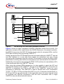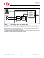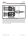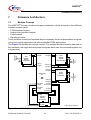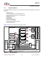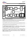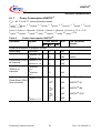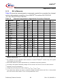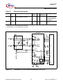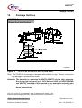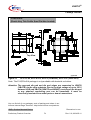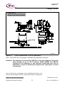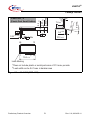
1
P r el i m i na ry P ro du ct O v er v i ew , R ev . 2.0 , M ay 2 00 4
VINETIC
®
Voice and Internet Enhanced
Telephony Interface Concept
PEB
PEB
PEB
PEB
PEB
PEB
PEB
PEB
PEB
PEB
PEB
PEB
PEB
PEB
3324
3322
3332
3320
3314
3394
3304
4264/-2
4364
4265/-2
4365
4266
4262
4268
Wireline
Communications
N e v e r
s t o p
t h i n k i n g .
ABM®, ACE®, AOP®, ARCOFI®, ASM®, ASP®, DigiTape®, DuSLIC®, EPIC®, ELIC®,
FALC®, GEMINAX®, IDEC®, INCA®, IOM®, IPAT®-2, ISAC®, ITAC®, IWE®, IWORX®,
MUSAC®, MuSLIC®, OCTAT®, OptiPort®, POTSWIRE®, QUAT®, QuadFALC®,
SCOUT®, SICAT®, SICOFI®, SIDEC®, SLICOFI®, SMINT®, SOCRATES®, VINETIC®,
10BaseV®, 10BaseVX® are registered trademarks of Infineon Technologies AG.
10BaseS™, EasyPort™, VDSLite™ are trademarks of Infineon Technologies AG.
Microsoft® is a registered trademark of Microsoft Corporation. Linux® is a registered
trademark of Linus Torvalds.
The information in this document is subject to change without notice.
Edition 2004-05-11
Published by Infineon Technologies AG,
St.-Martin-Strasse 53,
81669 München, Germany
© Infineon Technologies AG 5/14/04.
All Rights Reserved.
Attention please!
The information herein is given to describe certain components and shall not be considered as warranted
characteristics.
Terms of delivery and rights to technical change reserved.
We hereby disclaim any and all warranties, including but not limited to warranties of non-infringement, regarding
circuits, descriptions and charts stated herein.
Infineon Technologies is an approved CECC manufacturer.
Information
For further information on technology, delivery terms and conditions and prices please contact your nearest
Infineon Technologies Office in Germany or our Infineon Technologies Representatives worldwide
(www.infineon.com).
Warnings
Due to technical requirements components may contain dangerous substances. For information on the types in
question please contact your nearest Infineon Technologies Office.
Infineon Technologies Components may only be used in life-support devices or systems with the express written
approval of Infineon Technologies, if a failure of such components can reasonably be expected to cause the failure
of that life-support device or system, or to affect the safety or effectiveness of that device or system. Life support
devices or systems are intended to be implanted in the human body, or to support and/or maintain and sustain
and/or protect human life. If they fail, it is reasonable to assume that the health of the user or other persons may
be endangered.
Preliminary Product Overview
Revision History:
2004-05-11
Previous Version:
none
Page
Subjects (major changes since last revision)
VINETIC-2CPE added
Featurelist updated
Rev. 2.0
VINETIC®
Preface
This Preliminary Product Overview describes the Voice and Internet Enhanced
Telephony Interface Concept (VINETIC®) chip set family. For more VINETIC® related
documents, please see our webpage at http://www.infineon.com/vinetic.
To simplify matters, the following synonyms are used:
VINETIC®-x:
Synonym used for all codec versions VINETIC®-4VIP, VINETIC®-2VIP,
VINETIC®-2CPE, VINETIC®-4C, VINETIC®-4M, VINETIC®-4S,
VINETIC®-8S and VINETIC®-8M.
VINETIC®-4x:
Synonym used for 4-channel versions of the VINETIC® family. To
simplify matters only the 4-channel versions are depicted in this
document in most cases.
SLIC:
Synonym used for all SLIC versions SLIC-S/-S2, TSLIC-S, SLIC-E/-E2,
TSLIC-E, SLIC-P, SLIC-LCP and SLIC-DC.
Attention: The TSLIC-S (PEB 4364) and TSLIC-E (PEB 4365) chips are dual
channel versions of the SLIC-S (PEB 4264) and SLIC-E (PEB 4265) with
identical technical specifications for each channel. Therefore whenever
SLIC-S or SLIC-E are mentioned in the specification, also TSLIC-S and
TSLIC-E can be deployed.
Organization of this Document
This Preliminary Product Overview is divided into 11 chapters. It is organized as follows:
• Chapter 1, Family Overview
A general description of the chip set, the key features, and some typical applications.
• Chapter 2, VINETIC® Host Interface Description
Connection information including the different interface types.
• Chapter 3, Codec/SLIC Features (BORSCHT Functions)
The main functions of the chip set are presented with functional block diagrams.
• Chapter 6, Operating Modes
A brief description of the operating modes and the integrated test and diagnostic
functions.
• Chapter 4, Signalprocessing Capabilities of the VINETIC®
A short overview of DSP performance necessary for different algorithms.
• Chapter 5, Programming of the VINETIC®
A general description of the VINETIC®-x command structure.
• Chapter 7, Firmware Architecture
A general description of the VINETIC®-x software system
Preliminary Product Overview
4
Rev. 2.0, 2004-05-11
VINETIC®
• Chapter 8, Electrical Characteristics
Parameters, symbols, and limit values are provided for the chip set.
• Chapter 9, Application Circuits
External components are identified. Illustrations of balanced ringing, unbalanced
ringing, and protection circuits are included.
• Chapter 10, Package Outlines
Illustrations and dimensions of the package outlines.
• Chapter 11, Terminology
List of abbreviations and descriptions of symbols.
• Chapter 12, Index
Attention: This document is a pre release version of the VINETIC® product
overview.
Related Documentation
in preparation
Preliminary Product Overview
5
Rev. 2.0, 2004-05-11
VINETIC®
Table of Contents
Page
1
1.1
1.2
1.3
1.4
1.5
1.6
1.7
Family Overview . . . . . . . . . . . . . . . . . . . . . . . . . . . . . . . . . . . . . . . . . . .
Pin Diagram VINETIC®-4x . . . . . . . . . . . . . . . . . . . . . . . . . . . . . . . . . . . . .
P-LQFP-176-2 Pin Diagram . . . . . . . . . . . . . . . . . . . . . . . . . . . . . . . . . . . .
P-LBGA-176-3 Pin Diagram . . . . . . . . . . . . . . . . . . . . . . . . . . . . . . . . . . .
PG-LBGA-144 Pin Diagram (4-channel devices) . . . . . . . . . . . . . . . . . . .
PG-LBGA-144 Pin Diagram (2-channel devices) . . . . . . . . . . . . . . . . . . .
Logic Symbol VINETIC®-4x . . . . . . . . . . . . . . . . . . . . . . . . . . . . . . . . . . . .
Typical Applications . . . . . . . . . . . . . . . . . . . . . . . . . . . . . . . . . . . . . . . . . .
2
2.1
VINETIC® Host Interface Description . . . . . . . . . . . . . . . . . . . . . . . . . . . 26
VINETIC® Host Interface Configurations . . . . . . . . . . . . . . . . . . . . . . . . . . 26
3
3.1
3.2
3.2.1
3.2.2
3.2.3
Codec/SLIC Features (BORSCHT Functions) . . . . . . . . . . . . . . . . . . . .
BORSCHT functions . . . . . . . . . . . . . . . . . . . . . . . . . . . . . . . . . . . . . . . . .
Advanced Integrated Test and Diagnostic Functions (AITDF) . . . . . . . . .
Introduction . . . . . . . . . . . . . . . . . . . . . . . . . . . . . . . . . . . . . . . . . . . . . .
VINETIC® Line Testing . . . . . . . . . . . . . . . . . . . . . . . . . . . . . . . . . . . . .
Board and Production Testing . . . . . . . . . . . . . . . . . . . . . . . . . . . . . . . .
4
Signalprocessing Capabilities of the VINETIC® . . . . . . . . . . . . . . . . . . 31
5
5.1
5.2
5.3
5.4
5.4.1
5.4.2
5.5
5.6
Programming of the VINETIC® . . . . . . . . . . . . . . . . . . . . . . . . . . . . . . . .
Command/Data Structure in Downstream Direction . . . . . . . . . . . . . . . . .
Command/Data Structure in Upstream Direction . . . . . . . . . . . . . . . . . . .
First Command Word . . . . . . . . . . . . . . . . . . . . . . . . . . . . . . . . . . . . . . . . .
Second Command Word . . . . . . . . . . . . . . . . . . . . . . . . . . . . . . . . . . . . . .
Second Command Word in Case of SOP, COP and IOP . . . . . . . . . . .
Second Command Word in Case of EOP, EVT and VOP . . . . . . . . . . .
Data Words . . . . . . . . . . . . . . . . . . . . . . . . . . . . . . . . . . . . . . . . . . . . . . . .
Data Handling . . . . . . . . . . . . . . . . . . . . . . . . . . . . . . . . . . . . . . . . . . . . . .
6
6.1
6.2
Operating Modes . . . . . . . . . . . . . . . . . . . . . . . . . . . . . . . . . . . . . . . . . . . 39
Overview of all VINETIC® Operating Modes . . . . . . . . . . . . . . . . . . . . . . . 39
Automatic Modes for POTS Signaling and Power Management . . . . . . . . 41
7
7.1
7.2
7.3
7.4
7.5
7.6
Firmware Architecture . . . . . . . . . . . . . . . . . . . . . . . . . . . . . . . . . . . . . . .
Module Concept . . . . . . . . . . . . . . . . . . . . . . . . . . . . . . . . . . . . . . . . . . . . .
PCM-Interface Module . . . . . . . . . . . . . . . . . . . . . . . . . . . . . . . . . . . . . . . .
Analog-Line-Module ALM . . . . . . . . . . . . . . . . . . . . . . . . . . . . . . . . . . . . .
Signaling Module . . . . . . . . . . . . . . . . . . . . . . . . . . . . . . . . . . . . . . . . . . . .
Coder Module . . . . . . . . . . . . . . . . . . . . . . . . . . . . . . . . . . . . . . . . . . . . . .
Test Features . . . . . . . . . . . . . . . . . . . . . . . . . . . . . . . . . . . . . . . . . . . . . . .
8
8.1
Electrical Characteristics . . . . . . . . . . . . . . . . . . . . . . . . . . . . . . . . . . . . 52
Operating Range VINETIC® . . . . . . . . . . . . . . . . . . . . . . . . . . . . . . . . . . . 52
Preliminary Product Overview
6
10
17
17
18
19
20
21
22
28
28
29
29
29
30
33
33
35
36
36
36
37
37
37
42
42
44
45
46
49
51
Rev. 2.0, 2004-05-11
VINETIC®
Table of Contents
Page
8.1.1
8.1.2
8.2
8.3
8.4
8.5
8.6
8.7
8.8
Power Consumption VINETIC® . . . . . . . . . . . . . . . . . . . . . . . . . . . . . . .
Power-Up Sequence VINETIC® . . . . . . . . . . . . . . . . . . . . . . . . . . . . . .
Operating Range SLIC-S/-S2 . . . . . . . . . . . . . . . . . . . . . . . . . . . . . . . . . .
Operating Range SLIC-E/-E2 . . . . . . . . . . . . . . . . . . . . . . . . . . . . . . . . . .
Operating Range SLIC-P . . . . . . . . . . . . . . . . . . . . . . . . . . . . . . . . . . . . . .
Operating Range SLIC-DC . . . . . . . . . . . . . . . . . . . . . . . . . . . . . . . . . . . .
Operating Range SLIC-LCP . . . . . . . . . . . . . . . . . . . . . . . . . . . . . . . . . . .
AC Transmission VINETIC® . . . . . . . . . . . . . . . . . . . . . . . . . . . . . . . . . . .
DC Characteristics . . . . . . . . . . . . . . . . . . . . . . . . . . . . . . . . . . . . . . . . . . .
54
55
57
58
59
60
61
62
63
9
9.1
9.1.1
9.1.2
9.1.3
9.2
Application Circuits . . . . . . . . . . . . . . . . . . . . . . . . . . . . . . . . . . . . . . . . .
Internal Ringing (Balanced/Unbalanced) . . . . . . . . . . . . . . . . . . . . . . . . . .
Application Circuits for Internal Ringing . . . . . . . . . . . . . . . . . . . . . . . . .
Bill of Materials . . . . . . . . . . . . . . . . . . . . . . . . . . . . . . . . . . . . . . . . . . .
Application Circuits for Internal Ringing with DC/DC . . . . . . . . . . . . . . .
External Ringing . . . . . . . . . . . . . . . . . . . . . . . . . . . . . . . . . . . . . . . . . . . .
65
65
65
68
69
71
10
Package Outlines . . . . . . . . . . . . . . . . . . . . . . . . . . . . . . . . . . . . . . . . . . . 73
11
Terminology . . . . . . . . . . . . . . . . . . . . . . . . . . . . . . . . . . . . . . . . . . . . . . . 81
12
Index . . . . . . . . . . . . . . . . . . . . . . . . . . . . . . . . . . . . . . . . . . . . . . . . . . . . . 84
Preliminary Product Overview
7
Rev. 2.0, 2004-05-11
VINETIC®
List of Figures
Figure 1
Figure 2
Figure 3
Figure 4
Figure 5
Figure 6
Figure 7
Figure 8
Figure 9
Figure 10
Figure 11
Figure 12
Figure 13
Figure 14
Figure 15
Figure 16
Figure 17
Figure 18
Figure 19
Figure 20
Figure 21
Figure 22
Figure 23
Figure 24
Figure 25
Figure 26
Page
Block Diagram VINETIC®-4x . . . . . . . . . . . . . . . . . . . . . . . . . . . . . . . .
P-LQFP-176-2 Pin Diagram . . . . . . . . . . . . . . . . . . . . . . . . . . . . . . . . .
P-LBGA-176-3 Pin Diagram. . . . . . . . . . . . . . . . . . . . . . . . . . . . . . . . .
Logic Symbol VINETIC®-4x . . . . . . . . . . . . . . . . . . . . . . . . . . . . . . . . .
Residential Gateway / ATA / VoIP Router . . . . . . . . . . . . . . . . . . . . . .
IAD serving POTS and ISDN (European Version) . . . . . . . . . . . . . . . .
Cable Modem / Settop Box / SMTA / EMTA . . . . . . . . . . . . . . . . . . . .
Next Generation Access Network Linecard . . . . . . . . . . . . . . . . . . . . .
Module Concept . . . . . . . . . . . . . . . . . . . . . . . . . . . . . . . . . . . . . . . . . .
PCM-Interface Module . . . . . . . . . . . . . . . . . . . . . . . . . . . . . . . . . . . . .
Analog-Line-Module ALM . . . . . . . . . . . . . . . . . . . . . . . . . . . . . . . . . .
Signaling Module . . . . . . . . . . . . . . . . . . . . . . . . . . . . . . . . . . . . . . . . .
Coder Channel Module . . . . . . . . . . . . . . . . . . . . . . . . . . . . . . . . . . . .
Application Circuit Internal Ringing (balanced) for SLIC-E/-S . . . . . . .
Application Circuit Internal Ringing (balanced) for TSLIC-E/-S . . . . . .
Application Circuit Internal Ringing (bal. & unbal.) for SLIC-P . . . . . . .
Application Circuit Internal Ringing with DC/DC . . . . . . . . . . . . . . . . .
Application Circuit External Ringing for SLIC-LCP . . . . . . . . . . . . . . .
SLIC-S/-S2, SLIC-E/-E2, SLIC-P (PEB 426x) . . . . . . . . . . . . . . . . . . .
SLIC-S/-S2, SLIC-E/-E2, SLIC-P (PEB426x), SLIC-LCP (PEB 4262) .
TSLIC-S (PEB 4364), TSLIC-E (PEB 4365) . . . . . . . . . . . . . . . . . . . .
SLIC-DC (PEB 4268) . . . . . . . . . . . . . . . . . . . . . . . . . . . . . . . . . . . . . .
SLIC-DC (PEB 4268) . . . . . . . . . . . . . . . . . . . . . . . . . . . . . . . . . . . . . .
VINETIC®-4x (PEB33x4HL), VINETIC®-2VIP (PEB 3322HL) and
VINETIC®-0 (PEB3320HL) . . . . . . . . . . . . . . . . . . . . . . . . . . . . . . . . .
VINETIC®-4x (PEB33x4E), VINETIC®-2VIP (PEB 3322E) and
VINETIC®-0 (PEB3320E). . . . . . . . . . . . . . . . . . . . . . . . . . . . . . . . . . .
VINETIC®-2CPE (PEB 3332), VINETIC®-4M (PEB 3314),
VINETIC®-4C (PEB 3394), VINETIC®-4S(PEB 3304) . . . . . . . . . . . . .
Preliminary Product Overview
8
16
17
18
21
22
23
24
25
42
44
45
46
50
65
66
67
69
72
73
74
75
76
77
78
79
80
Rev. 2.0, 2004-05-11
VINETIC®
List of Tables
Table 1
Table 2
Table 3
Table 4
Table 5
Table 6
Table 7
Table 8
Table 9
Table 10
Table 11
Table 12
Table 13
Table 14
Table 15
Table 16
Table 17
Page
VINETIC®-x Versions. . . . . . . . . . . . . . . . . . . . . . . . . . . . . . . . . . . . . .
SLIC Versions . . . . . . . . . . . . . . . . . . . . . . . . . . . . . . . . . . . . . . . . . . .
VINETIC® Features . . . . . . . . . . . . . . . . . . . . . . . . . . . . . . . . . . . . . . .
Provided Algorithms for VINETIC® . . . . . . . . . . . . . . . . . . . . . . . . . . .
Operating Range VINETIC® . . . . . . . . . . . . . . . . . . . . . . . . . . . . . . . .
Power Consumption VINETIC® . . . . . . . . . . . . . . . . . . . . . . . . . . . . . .
Power-Up Sequence VINETIC®. . . . . . . . . . . . . . . . . . . . . . . . . . . . . .
Operating Range SLIC-S/-S2 . . . . . . . . . . . . . . . . . . . . . . . . . . . . . . .
Operating Range SLIC-E/-E2 . . . . . . . . . . . . . . . . . . . . . . . . . . . . . . .
Operating Range SLIC-P . . . . . . . . . . . . . . . . . . . . . . . . . . . . . . . . . . .
Operating Range SLIC-DC . . . . . . . . . . . . . . . . . . . . . . . . . . . . . . . . .
Operating Range SLIC-LCP . . . . . . . . . . . . . . . . . . . . . . . . . . . . . . . .
AC Transmission . . . . . . . . . . . . . . . . . . . . . . . . . . . . . . . . . . . . . . . . .
DC Characteristics . . . . . . . . . . . . . . . . . . . . . . . . . . . . . . . . . . . . . . . .
External Components in Application Circuit for 4 Channels . . . . . . . .
Components for SLIC-DC Application Circuit . . . . . . . . . . . . . . . . . . .
External Components . . . . . . . . . . . . . . . . . . . . . . . . . . . . . . . . . . . . .
Preliminary Product Overview
9
12
12
13
31
52
54
55
57
58
59
60
61
62
63
68
69
71
Rev. 2.0, 2004-05-11
VINETIC®
Family Overview
1
Family Overview
The VINETIC® is a family of devices for analog telephone line provision. VINETIC®
devices are available in different granularity (0, 2, 4 and 8 analog voice channels) and
also with different levels of DSP performance (VIP, CPE, M, C, S). The seamless
connection to a broad range of SLICs provides the most effective solution for a wide
range of applications, from high density CO/DLC/PBX linecards to low-cost CPE
applications. Significant boardspace reduction can be achieved through the integrated
DSP for voice processing and packetization.
The VINETIC® provides system solutions for the following applications:
• Access Network:
– Central Office - TDM
– Digital Loop Carrier - TDM, VoATM, VoIP
– FTTH - TDM, VoATM, VoIP
– WLL - TDM, VoIP
• PBX:
– Analog Linecard - TDM, VoIP
• Customer Premises Equipment:
– Residential Gateway / Home Gateway / Internet Telephony Gateway (ITG) - VoIP
– Integrated Access Device (IAD) - VoIP, VoATM
– Cable Modems / Media Terminal Adapter (MTA) - VoIP
– Analog Telephony Adapter (ATA) - VoIP
To cover these applications, the VINETIC® devices are pin- and software-compatible,
allowing the maximum flexibility while offering the optimized feature set per application.
Preliminary Product Overview
10
Rev. 2.0, 2004-05-11
Voice and Internet Enhanced Telephony Interface Concept
VINETIC®
Executive Summary
The VINETIC® family integrates the DSP and RAM for
voice processing into the codec/SLIC chip set, thereby
offering a unique set of features for voice over packet:
• Cost and Boardspace Reduction - codec, DSP and
RAM are integrated into one small package providing
significant cost and boardspace advantages.
• Scalability - VINETIC® supports each voice channel
with the necessary amount of DSP performance due to
the encapsulation of codec and DSP.
• Flexibility - the VINETIC® family offers 2 to 8 analog
ports and various level of DSP performance, while
remaining pin- and software-compatible.
• World-Wide-Usage - The VINETIC® can be adapted
to different country requirements without a hardware
change (AC and DC path, ringing, metering, etc. are
programmable).
• Future Proof - the integrated RAM for downloading
advanced codecs or Infineon DSP software
guarantees that for future remote updates the system
will remain state-of-the-art technology.
• Designed for Voice over Packet (VoIP, VoDSL, Cable,
VoATM)
VINETIC
P-LQFP-176-2
P-LBGA-176-3 and PG-LBA-144-1
P-LBGA-176-2
SLIC
P-DSO-20-5
P-DSO-24-1, -3
P-VQFN-48-4
P-TQFP-48-1
TSLIC
P-DSO-36-15
Type
Package
PEB 3324, PEB 3322, PEB 3332,
PEB 3320, PEB 3314, PEB 3394,
PEB 3304
P-LQFP-176-2, P-LBGA-176-3,
PG-LBGA-144
PEB
Type4364, PEB 4365
PEB
4264/-2,
<Device
1> PEB 4265/-2, PEB 4266
P-DSO-36-15
Package
P-DSO-20-5,
P-LQFP-176-2P-VQFN-48-4
PEF
PEB 4268
3324
P-DSO-24-1,
P-DSO-20-5 -3, P-TQFP-48-1
Preliminary Product Overview
11
Rev. 2.0, 2004-05-11
VINETIC®
Family Overview
Table 1
VINETIC®-x Versions
Chip Set1)
VINETIC®4VIP
VINETIC®2VIP
VINETIC®2CPE
VINETIC®0
VINETIC®4M/-8M
VINETIC®4C
VINETIC®4S/-8S
Product ID
PEB 3324
PEB 3322
PEB 3332
PEB 3320
PEB 3314/
PEB 3318
PEB 3394
PEB 3304/
PEB 3308
Analog Channels
4
2
2
0
4/8
4
4/8
Echo Cancellation (G.165,
G.168)
up to
128 ms
up to
128 ms
up to
16 ms
up to
128 ms
up to 16 ms up to 16 ms
No
ADPCM (G.726)
Yes
Yes
Yes
Yes
Yes
Yes
No
Complex Voice Codecs
(G.723, G.728, G.729)2)
Yes
Yes
Yes
Yes
No
No
No
Yes
Yes
Yes
Yes
No
No
No
Signal processing functions
Yes
Yes
Yes
Yes
Yes
Yes
No
AAL2, RTP packetization,
Jitter Buffer
Yes
Yes
RTP only
Yes
Yes
No
No
Integrated Code RAM for
Firmware Download
Yes
Yes
Yes
Yes
Yes
No6)
No´6)
Line testing AITDF4)
Yes
Yes
GR909 only Yes
Yes
Yes
Yes
World wide programmability of
analog BORSCHT5) functions
Yes
Yes
Yes
Yes
Yes
Yes
Fax Relay T.38
3)
–
1)
All 4-, 2- and 0-channel devices are pin- and software compatible, except the VINETIC-2CPE that is optimized for CPE market;
for 8-channel codecs contact local sales.
2)
Patent indemnification available.
3)
e.g. DTMF generation and detection, Caller ID (CLIP) generation (FSK), Universal Tone Detection (UTD), Answering Tone
Detection (ATD), Caller-ID detection, Universal Tone Generator (covering Japanese Tones), Call Progress Tone detector.
4)
Advanced Integrated Test and Diagnosis Functions.
5)
Battery feed, Ringing, Signaling (supervision), Coding, Hybrid for 2/4-wire conversion, Testing, Hook thresholds, Teletax
metering.
6)
Versions up to v1.4 provide also RAM for firmware download
SLIC Versions1)
Table 2
Marketing
Name
SLIC-S
TSLIC-S
SLIC-S2
SLIC-E
TSLIC-E
SLIC-E2
SLIC-P
SLIC-LCP
SLIC-DC
Product ID
PEB 4264
PEB 4364
PEB 4264
-22)
PEB 4265
PEB 4365
PEB 4265
-23)
PEB 4266
PEB 4262
PEB 4268
Channels
1
2
1
1
2
1
1
1
1
Internal
Ringing
45 Vrms
balanced
45 Vrms
balanced
45 Vrms
balanced
85 Vrms
balanced
85 Vrms
balanced
85 Vrms
balanced
85 Vrms
bal.,
50 Vrms
unbal.
external
ringing
DC/DC
generator
included
60Vrms
Longitudinal
Balance
53 dB
53 dB
60 dB
53 dB
53 dB
60 dB
53 dB
60dB with
adaption
to external
components
48 dB
Maximum
DC feeding
32 mA
32 mA
50 mA
32 mA
32 mA
50 mA
32 mA
50 mA
32 mA
Neg. Battery
Voltages
2
2
2
2
2
2
2/3
2
0
Preliminary Product Overview
12
Rev. 2.0, 2004-05-11
VINETIC®
Family Overview
SLIC Versions1) (cont’d)
Table 2
Add. positive
Voltages
1
1
1
1
1
1
0
0
1
(unreg.
12-35V)
Technology
90 V
Smart
Power
90 V
Smart
Power
90 V
Smart
Power
170 V
Smart
Power
170 V
Smart
Power
170 V
Smart
Power
170 V
Smart
Power
170 V
Smart
Power
170 V
Smart
Power
1)
For broadband SLICs for the Infineon ADSL combo solution (Integrated Voice and Data IVD - GEMINAX-S
PEB 4561 and GEMINAX-S MAX PEF 55801), please contact local sales.
2)
Chip marked as PEB 4264
3)
Chip marked as PEB 4265
VINETIC® Features
Table 3
-VIP
-2
CPE
-C
-S
-0
VINETIC® Features
4/8
4
4/8
0
Number of fully programmable codecs with enhanced signal processing capabilities1)
(
(
(
(
Pin-compatible and software compatible
(
(
(
-M
Common Features
2/4
2
(
(
(
Glueless interface to Infineon SLICs family: SLIC-S/-S2, TSLIC-S, SLIC-E/-E2, TSLIC-E
and SLIC-P, SLIC-LCP and SLIC-DC2), GEMINAX-S, GEMINAX-S MAX
Integrated DSP Features
(
Integrated DSP
– with RAM for VoIP/VoDSL/VoATM and software download capability3)
(
(
(
(
(
(
(
(
(
(
RTP packetization & jitter buffer (adaptive and fixed; 200ms)
(
(
(
(
RTCP support
(
(
(
AAL2 cell generation & jitter buffer (adaptive and fixed; 200ms)
(
(
(
Compatible with ITU-T I.366.2
(
(
–
for enhanced signal processing
(
(
(
(
Compatible with RFC 1889 specification
(
(
(
(
Compatible with Packet Cable specification
(
(
PacketOverPCM functionality
(
Integrated DTMF generator
(
(
(
(
(
(
(
(
(
(
Integrated DTMF decoder
(
(
(
(
(
Integrated Caller ID (FSK) generator, according to Bellcore 202 and V.23
(
(
(
(
(
Integrated Caller ID (FSK) detector, according to Bellcore 202 and V.23
(
(
(
(
(
Integrated fax/modem detection by Universal Tone Detection unit (UTD), In-band tone
detection
(
(
(
(
(
Integrated Universal Tone Generator (UTG) including holwer tone and japanese tone
generation
(
(
(
(
(
Call Progress Tone (CPT) Detector
(
(
(
(
(
Preliminary Product Overview
Optimized filter structure for modem transmission, enhanced modem performance for
improvement of V.90 transmission
13
Rev. 2.0, 2004-05-11
VINETIC®
Family Overview
VINETIC® Features (cont’d)
Table 3
-0
VINETIC® Features
(
Multi-party conferencing
(
3-Party conferencing via packet network
(
G.711
(
G.711 Annex I (Packet Loss Concealment), G.711 Annex II (VAD + CNG)
(
G.726 ADPCM
(
(
G.729 A, B
(
(
(
G.723.1
(
(
(
G.728, G.728 Annex I (Packet Loss Concealment)
(
(
(
G.729 E
(
(
(
iLBC4)
(
(
(
(
Voice Activity Detection (VAD)
(
(
(
(
Comfort Noise Generation (CNG)
(
(
Algorithms for Line Echo Cancellation exceeding G.165, G.168, G.168-2000, G.168-2002:
– up to 128 ms tail length
– up to 16 ms tail length
(
Voice Play Out (reordering, fixed and adaptive jitter buffer, clock synchronization)
-VIP
-2
CPE
-M
-C
(
(
(
(
(
(
(
(
(
(
(
(
(
(
(
(
(
(
-S
(
(
(
(
(
(
(
(
(
(
(
(
T.38 Fax Relay Support including all required datapump algorithms V.17, V.21, V.27ter,
V.29
(
(
(
Text phone support V.18
(
Codec/SLIC Features
(
(
(
(
(
Worldwide programmability for AC and DC parameters
(
(
(
(
(
Specification in accordance with ITU-T Recommendation Q.552 for interface Z
(
(
(
Specification in accordance with ITU-T Recommendation G.712,
and applicable LSSGR(GR-506/507 etc.), GR-57, EIA/TIA-464 and other applicable
worldwide standards.
(
(
(
Integrated balanced/unbalanced ringing capability fully software programmable up to
85 Vrms ringing voltage, Crest-factor selection between 1.2 and 1.6, frequency range
between 15 and 75Hz
(
(
(
(
External ringing support
(
(
(
(
Programmable 12/16 kHz teletax generation (metering) and integrated notch filtering
(
(
(
(
(
(
(
(
Programmable battery feeding with capability for driving longer loops
(
(
(
(
(
Ground/loop start signaling
(
(
(
Ground key detection
(
(
(
(
(
(
Polarity reversal
(
(
(
(
(
Message Waiting Indication
(
(
(
(
(
Automatic modes for POTS signaling and Power Management
(
(
(
(
(
Advanced Integrated Test and Diagnostic Functions (AITDF) for local loop monitoring
(including GR-909) and board production test capabilities.
(
(
(
(
(
On-hook transmission
Preliminary Product Overview
14
Rev. 2.0, 2004-05-11
VINETIC®
Family Overview
VINETIC® Features (cont’d)
Table 3
-VIP
-2
CPE
-M
-C
-S
(
(
(
(
(
(
(
(
(
(
(
(
(
(
-0
VINETIC® Features
Power optimized architecture with power management capability (integrated battery
switches)
(
Part of ADSL IVD and IPVD solution
Direct connection of Clare Litelink III device
Interface Features
(
(
(
(
(
(
PCM/µC interface selectable
2
1
2
2
2
2
PCM interface (number of highways)
(
(
(
(
(
(
Parallel Host interface: Intel/Motorola compatible
(
(
(
(
(
(
Serial control interface, SCI (Infineon) compatible, SPI compatible
(
(
(
(
(
(
(
(
(
(
(
JTAG interface for boundary scan
SLIC interface compatible with DuSLIC® SLICs
Available Packages5)
(
(
(
(
(
(
P-LQFP-176
(
(
(
(
(
(
P-LBGA-176
(
(6)
()6
()6
PG-LBGA-144
Additional Features
(
(
(
(
(
(
(
(
(
SW compatible between different VINETIC devices
(
(
(
(
HW compatible between different VINETIC devices
(
(
(
(
Driver and API for Linux and VxWorks
1)
8-channel devices in preparation
2)
In preparation.
3)
All VINETIC® devices up to version v1.4 include RAM for download
4)
in preparation
5)
Green Packages in preparation, contact local sales for details
6)
only available for production from v2.1 onwards
Preliminary Product Overview
15
Rev. 2.0, 2004-05-11
VINETIC®
Family Overview
BUS
ANALOGLINEMODULE
(2 channels)
128 MHz
ANALOGLINEMODULE
(2 channels)
serial /
parallel
interface
PCM
BUS
SLIC
SLIC
SLIC
SLIC
128 MHz
HOST
PLL,
Clock Control
32 MHz
Programmable Host Interface
(PHI)
VINETIC-4x
Extended DSP
(EDSP)
ROM/RAM
Vinetic_0001_Vinetic_Blockdiagram
Figure 1
Block Diagram VINETIC®-4x
Figure 1 shows the typical block diagram of a VINETIC® 4-channel device.
Preliminary Product Overview
16
Rev. 2.0, 2004-05-11
VINETIC®
Family Overview
Pin Diagram VINETIC®-4x
1.2
P-LQFP-176-2 Pin Diagram
IO1D
IO2D
IO3D
IO4D
CDCND
DCND
DCPD
CDCPD
VDD18D
GNDD
VDD33D
ITACD
VCMITD
ITD
ILD
ACND
ACPD
C2D
C1D
VCMCD
VREFCD
VDD18CD
GNDCD
VDD33CD
CREFCD
C1C
C2C
ACPC
ACNC
ILC
ITC
VCMITC
ITACC
VDD33C
GNDC
VDD18C
CDCPC
DCPC
DCNC
CDCNC
IO4C
IO3C
IO2C
IO1C
1.1
I/O D
90
95
100
105
110
115
120
125
130
Analog Channel D
Analog Channel C
85
JTAG /
TMSEL
135
I/O C
140
80
145
PCM
75
150
Host Interface
70
GPIO
155
160
60
165
55
IFSELECT
50
I/O A
40
25
20
15
10
5
1
175
35
Analog Channel B
Analog Channel A
30
170
65
45
I/O B
IO0C
VDD33
GND
MCLK
INTQ
IFC8
IFC7
VDD18P
GNDP
VDD33
GND
VDD18
IFAD15
IFAD14
IFAD13
IFAD12
IFAD11
IFAD10
IFAD9
IFAD8
VDD18
GND
VDD33
IFAD7
IFAD6
IFAD5
IFAD4
IFAD3
IFAD2
IFAD1
IFAD0
VDD18
GND
VDD33
IFC6
IFC5
IFC4
IFC3
IFC2
IFC1
IFC0
GND
VDD33
IO0B
IO1A
IO2A
IO3A
IO4A
CDCNA
DCNA
DCPA
CDCPA
VDD18A
GNDA
VDD33A
ITACA
VCMITA
ITA
ILA
ACNA
ACPA
C2A
C1A
CREFAB
VDD33AB
GNDAB
VDD18AB
VREFAB
VCMAB
C1B
C2B
ACPB
ACNB
ILB
ITB
VCMITB
ITACB
VDD33B
GNDB
VDD18B
CDCPB
DCPB
DCNB
CDCNB
IO4B
IO3B
IO2B
IO1B
IO0D
VDD33
GND
TDO/TM3
TCK/TM2
TMS/TM1
TDI/TM0
TDRS
TEST
VDD33
GND
VDD18
TC2Q
DX2
DR2
FSC
PCL
TC1Q
DX1
DR1
VDD18
GND
VDD33
GPIO0
GPIO1
GPIO2
GPIO3
GPIO4
GPIO5
GPIO6
GPIO7
VDD18
GND
VDD33
IFSEL3
IFSEL2
IFSEL1
IFSEL0
RSYNC
RESETQ
AUX
GND
VDD33
IO0A
Vinetic_0000_pinning_diagram
Figure 2
P-LQFP-176-2 Pin Diagram
Preliminary Product Overview
17
Rev. 2.0, 2004-05-11
VINETIC®
Family Overview
1.3
P-LBGA-176-3 Pin Diagram
A
B
C
D
E
F
G
H
J
K
L
M
N
P
R
VSS
IO1D
IO3D
DCPD
VDD33D
ILD
C1D
GNDCD
C1C
ITC
GNDC
DCNC
CDCNC
IO4C
IO2C
TDO/TM3
IO0D
IO2D
DCND
GNDD
ITD
C2D
VREFCD
C2C
ILC
VDD33C
DCPC
IO3C
IO1C
IO0C
TCK/TM2
VDD33
TMS/TM1
CDCND
VDD18D
VCMITD
ACPD
VDD18CD CREFCD
ACNC
ITACC
CDCPC
VSS
VDD33
MCLK
TDI/TMO
TDRS
TEST
IO4D
CDCPD
ITACD
ACND
VCMCD VDD33CD
ACPC
VCMITC
VDD18C
VDD18P
INTQ
IFC7
VDD33
VSS
VDD18
TC2Q
IFC8
VSSP
VSS
VDD33
DX2
DR2
FSC
PCL
VDD18
IFAD15
IFAD13
IFAD14
TC1Q
DX1
DR1
VDD18
IFAD12
IFAD11
IFAD9
IFAD10
VDD33
GPIO0
VSS
GPIO1
IFAD8
VDD18
VDD33
VSS
GPIO3
GPIO2
GPIO4
GPIO5
IFAD7
IFAD6
IFAD3
IFAD5
GPIO7
GPIO6
VDD18
VSS
IFAD4
IFAD2
IFAD0
IFAD1
VDD33
IFSEL3
IFSEL2
IFSEL1
VDD18
VSS
IFC6
VDD33
RSYNC
IFSEL0
RESETQ
VDD18A
VCMITA
ACPA
VDD33AB
GNDAB
ACPB
ILB
VDD33B
IO4B
IFC5
IFC4
IFC3
AUX
IO0A
IO4A
CDCPA
ITACA
ACNA
CREFAB
VCMAB
ACNB
ITACB
CDCPB
DCPB
VDD33
VSS
IFC2
VSS
IO1A
IO2A
DCNA
VDD33A
ILA
C1A
VREFAB
C1B
VCMITB
VDD18B
CDCNB
IO1B
IO0B
IFC1
VDD33
IO3A
CDCNA
DCPA
GNDA
ITA
C2A
VDD18AB
C2B
ITB
GNDB
DCNB
IO3B
IO2B
IFC0
15
14
13
12
11
10
9
8
7
6
5
4
3
2
1
Vinetic_0000a_LBGA_pinning_diagram
Figure 3
P-LBGA-176-3 Pin Diagram
Preliminary Product Overview
18
Rev. 2.0, 2004-05-11
VINETIC®
Family Overview
1.4
PG-LBGA-144 Pin Diagram (4-channel devices)
A
B
C
D
E
F
G
H
J
K
L
M
IO1D
IO2D
CDCPD
DCPD
ACND
ACPD
ACPC
ACNC
DCPC
CDCPC
IO2C
IO1C
IO4D
IO3D
CDCND
ITACD
VDD33A
C2D
VDD18A
VDD33A
ITACC
CDCNC
IO3C
IO4C
C1D
ITD
DCND
VCMITD
ILD
VREFCD
C2C
ILC
VCMITC
DCNC
ITC
C1C
TDRSQ
TDI/TM0
TMS/TM1
TEST
IO0D
VCMCD
CREFCD
IO0C
TDO/TM3
INTQ
GNDP
VDD18P
VDD33
VDD18
TC2Q
TCK/TM2
Dx2
GNDA
GNDA
IFC8
PCL
IFAD4
IFAD7
VDD33
DR1
DX1
FSC
DR2
TC1Q
GND
GND
IFC7
IFC4
IFAD6
IFAD5
VDD18
GPIO0/
SCDO
GPIO1/
SCDI
GPIO2/
SCCK
GPIO3
GPIO4
GND
GND
GPIO7
IFC0
IFAD2
IFAD3
VDD18
VDD33
VDD18
GPIO6
RSYNC
AUX
GNDA
GNDA
GPIO5
IFC2
IFAD0
IFAD1
VDD33
IFSEL2
IFSEL0
IFSEL1
RESETQ
IO0A
CREFAB
VCMAB
IO0B
IFC3
IFC1
IFC5
IFC6
C1A
ITA
DCNA
VCMITA
ILA
C2A
VREFAB
ILB
VCMITB
DCNB
ITB
C1B
IO4A
IO3A
CDCNA
ITACA
VDD33A
VDD18A
C2B
VDD33A
ITACB
CDCNB
IO3B
IO4B
IO1A
IO2A
CDCPA
DCPA
ACNA
ACPA
ACPB
ACNB
DCPB
CDCPB
IO2B
IO1B
12
11
10
9
8
7
6
5
4
3
2
1
Vinetic_0000a_HDLC_LBGA_144_pinning_diagram_21
Preliminary Product Overview
19
Rev. 2.0, 2004-05-11
VINETIC®
Family Overview
1.5
PG-LBGA-144 Pin Diagram (2-channel devices)
A
B
C
D
E
F
G
H
J
K
L
M
dnc
dnc
dnc
dnc
dnc
dnc
dnc
dnc
dnc
dnc
dnc
dnc
dnc
dnc
dnc
ITACD
VDD33A
dnc
VDD18A
VDD33A
ITACC
dnc
dnc
dnc
dnc
ITD
dnc
VCMITD
ILD
dnc
dnc
ILC
VCMITC
dnc
ITC
dnc
TEST
dnc
dnc
dnc
dnc
TDO/TM3
INTQ
GNDP
VDD18P
12
11
10
TDRSQ
TDI/TM0 TMS/TM1
VDD33
VDD18
dnc
TCK/TM2
DR1
GNDA
GNDA
IFC8
PCL
IFAD4
IFAD7
VDD33
DR1
DX1
FSC
DX1
dnc
GND
GND
IFC7
IFC4
IFAD6
IFAD5
VDD18
GPIO0
GPIO1
GPIO2
GPIO3
GPIO4
GND
GND
GPIO7
IFC0
IFAD2
IFAD3
VDD18
VDD33
VDD18
GPIO6
RSYNC
AUX
GNDA
GNDA
GPIO5
IFC2
IFAD0
IFAD1
VDD33
IFSEL2
IFSEL0
IFSEL1
RESETQ
IO0A
CREFAB
VCMAB
IO0B
IFC3
IFC1
IFC5
IFC6
C1A
ITA
DCNA
VCMITA
ILA
C2A
VREFAB
ILB
VCMITB
DCNB
ITB
C1B
IO4A
IO3A
CDCNA
ITACA
VDD33A
VDD18A
C2B
VDD33A
ITACB
CDCNB
IO3B
IO4B
IO1A
IO2A
CDCPA
DCPA
ACNA
ACPA
ACPB
ACNB
DCPB
CDCPB
IO2B
IO1B
9
8
7
6
5
4
3
2
1
Vinetic_0000a_2CPE_LBGA_144_pinning_diagram
Preliminary Product Overview
20
Rev. 2.0, 2004-05-11
VINETIC®
Family Overview
1.6
Logic Symbol VINETIC®-4x
4
Line
current
4
4
4
4
DC
loop
4
4
4
AUX
TEST
TDRSQ
ITx
ITACx
ILx
VCMITx
DCPx
DCNx
IFSEL0..3
CDCPx
CDCNx
4
4
Logic
control
4
4
4
4
4
I/O's
4
4
ACPx
ACNx
4
4
10
6
10
serial
interface
(SCI/SPI)
IFC6
IFC7
IFAD0
IFAD1
IFAD2
IFAD3
IFAD4
IFAD5
IFAD6
IFAD7
IFAD8
IFAD9
IFAD10
IFAD11
IFAD12
IFAD13
IFAD14
IFAD15
IFC0
IFC1
IFC2
IFC3
IFC4
IFC5
IFC8
IO0x
IO1x
IO2x
IO3x
IO4x
VDD33x
GNDx
VDD18x
VDD33AB
VDD33CD
VDD18AB
VDD18CD
GNDAB
GNDCD
Power
supply
PCM
interface
INTQ
C1x
C2x
CREFAB
CREFCD
4
4
MCLK
TC1Q
TC2Q
DR1
DX1
DR2
DX2
PCL
FSC
VCMAB
VCMCD
VREFAB
VREFCD
AC
loop
JTAGinterface /
testmode
select
TDI/TM0
TMS/TM1
TCK/TM2
TDO/TM3
VDD33
VDD18
GND
VDD18P
GNDP
GPIOn
x ... synonym for channel A, B, C, D
n ... synonym for 0 ... 7
Intel- /
Motorola
interface
8
RESETQ
RSYNC
Vinetic_0018_logic_symbol
Figure 4
Logic Symbol VINETIC®-4x
Preliminary Product Overview
21
Rev. 2.0, 2004-05-11
VINETIC®
Family Overview
1.7
Typical Applications
The following applications are only a small part of the numerous possibilities when using
the VINETIC® chip set:
Wireless
LAN
Mini-PCI
connection
Network
Processor
10/100bT
Ethernet
Parallel µC IF
POTS lines
t/r
SLIC
DSP
t/r
optional
SLIC
SLIC
VINETIC
-2CPE/-4VIP
VINETIC
optional
Clare
DAA
PSTN
vinetic_residential_gateway
Figure 5
Residential Gateway / ATA / VoIP Router
Figure 5 shows a residential gateway that allows to extend the home network by
introducing VoIP and a wireless data connection to it. The existing Ethernet connection
is terminated by a network processor that enables additional functionality like firewalling,
routing, and other data services as well as the voice call control. To keep the network as
optimized as possible, the VINETIC®-2CPE for two voice channels or the
VINETIC®-4VIP for four channels takes care of all the functionality that is voice related.
All jitter buffering, RTP packetization, tone generation and detection including event
handling and voice processing (compression G.72x, T.38 fax relay modem modulations,
line echo cancellation) is handled within the DSP of the VINETIC®. No external memory
or other components is needed. All the analog functionality is covered at the same time,
including ringing, feeding, line testing, and supervision. The number of POTS lines can
easily be increased by adding more VINETIC® devices if desired.
For an FXO operation to connect to the PSTN network, the VINETIC® devices allow
direct connection to DAAs and provide all necessary signal processing functionality like
Caller-ID detection.
Preliminary Product Overview
22
Rev. 2.0, 2004-05-11
VINETIC®
Family Overview
10/100bT
Ethernet
4 POTS lines
t/r
t/r
parallel
µC IF
SLIC
DSP
PCM
SLIC
t/r
SLIC
t/r
SLIC
VINETIC
-4VIP/-4M
Network
Processor
Utopia
Socrates-U
SHDSL
VINETIC
S-if
ISAC-SX
S-if
ISAC-SX
(optional)
Par. Host Interface
vinetic_IAD_POTS_ISDN
Figure 6
IAD serving POTS and ISDN (European Version)
Figure 6 shows an highly integrated G.SHDSL Integrated Access Device (IAD). The
application consists of four major blocks: the SHDSL-transceiver, the network controller,
the ISDN S-transceiver (the ISAC-SX devices are an option for european IADs), and the
POTS part including voice processing (VINETIC®).
Analog signals from the POTS telephones are terminated within the VINETIC® chip set
and then digitized. In a next step these signals are packetized and sent via tha
microprocessor interfaces to the host controller. All necessary fucntions for AAL2 or RTP
packetization including jitter buffer and compression are executed within the VINETIC®.
Additionally voice and tone processing like DTMF, CLIP and line echo cancellation (LEC)
is also performed within the VINETIC® chip set.
When using the optional ISDN transceivers it is also possible to apply the LEC and
compression features of the VINETIC® chip set to the ISDN channels. Voice from the
ISAC-SX is transferred via PCM to the DSP of the VINETIC®, where the voice
processing is performed. The VINETIC® is able to handle both voice compression
(G.723.1, G.728 or G.729) and Near End LEC for up to 4 channels simultaneously or
G.726 and LEC for up to 8 channels. In the application above all voice channels could
be operated with ADPCM compression and line echo cancellation with a single
VINETIC® chip set without external memory.
Preliminary Product Overview
23
Rev. 2.0, 2004-05-11
VINETIC®
Family Overview
Ethernet
10/100bT
Network
Processor
µC IF
Cable Modem
Transceiver
POTS lines
t/r
t/r
Cable
SLIC
SLIC
VINETIC
-2CPE
VINETIC
Figure 7
Cable Modem / Settop Box / SMTA / EMTA
The VINETIC® chip set fulfills all requirements for packetized voice over cable (see
Figure 7). The voice data is transferred in RTP packets, allowing the network processor
an easy packetization for transmitting it via VoIP over the cable network. The VINETIC®
system is conform to PacketCable specification.
Fax-relay T.38 is also supported by the VINETIC® chip set. No additional DSP for voice
processing or fax termination is needed in the system.
Preliminary Product Overview
24
Rev. 2.0, 2004-05-11
VINETIC®
Family Overview
8..xx POTS lines
t/r
t/r
t/r
t/r
t/r
t/r
t/r
t/r
SLIC
SLIC
SLIC
SLIC
parallel µC IF
VINETIC
-4x
SLIC
SLIC
SLIC
SLIC
VINETIC
-4x
VINETIC
t/r
t/r
t/r
t/r
t/r
t/r
t/r
t/r
Network
Processor
PHY
ATM / IP
(Packets)
SLIC
SLIC
SLIC
SLIC
VINETIC
-4x
SLIC
SLIC
SLIC
SLIC
VINETIC
-4x
PCM
VINETIC
vinetic_NextG_Acc
Figure 8
Next Generation Access Network Linecard
Next generation Access Networks / DLCs are using ATM or IP networks to transmit data
and voice. VINETIC® is highly scalable and allows to install as many codecs in parallel
as required by the linecard design. The integrated line testing, ring generation and small
footprint SLIC chips makes VINETIC® an optimum fit for these high density applications.
Both RTP and AAL2 are supported by VINETIC® enabling the network processor to have
either an IP or an ATM backbone.
Preliminary Product Overview
25
Rev. 2.0, 2004-05-11
VINETIC®
VINETIC® Host Interface Description
VINETIC® Host Interface Description
2
The host interface of the VINETIC® is operated by a programmable host interface
controller (PHI) which allows a flexible and easy adaption to various interface types. For
programming the VINETIC® and performing data/packet transfer from/to VINETIC® a
parallel interface or a serial microcontroller interface can be used. Additionally VINETIC®
has an interface to PCM data.
VINETIC® 8/16-Bit Parallel Interfaces
The parallel interface can be operated in Intel 8/16-bit mode (multiplexed/demultiplexed)
or in 8/16-bit Motorola mode.
Note: VINETIC®-2CPE and VINETIC® devices with PG-LBGA-144 package only
support 8-bit interfaces
VINETIC® Serial Interfaces
The VINETIC® serial microcontroller interface (µC interface = SCI) is compatible with
Motorola SPI and is electrically compatible with DuSLIC®. The PCM interface has 2 PCM
highways and can be operated together with the serial µC interface or the parallel
interface.
Note: VINETIC®-2CPE only supports one PCM interface
2.1
VINETIC® Host Interface Configurations
The VINETIC® host interface can be set into one of the following modes:
•
•
•
•
•
•
•
8-bit INTEL multiplexed mode + PCM interface (2 PCM highways)
8-bit INTEL demultiplexed mode + PCM interface (2 PCM highways)
16-bit INTEL multiplexed mode + PCM interface (2 PCM highways)
16-bit INTEL demultiplexed mode + PCM interface (2 PCM highways)
8-bit MOTOROLA mode + PCM interface (2 PCM highways)
16-bit MOTOROLA mode + PCM interface (2 PCM highways)
VINETIC® serial µC interface (compatible with Motorola SPI and DuSLIC®) + PCM
interface (2 PCM highways)
Note: VINETIC®-2CPE only supports 8-bit and serial interfaces with only one PCM
highway
Note: VINETIC® devices with PG-LBGA-144 package only support 8-bit interfaces
Data transfers to and from the VINETIC® are either performed via a mailbox system and
via the controller interface, or via PacketOverPCM.
The VINETIC® supports the widely used microcontrollers: e.g. ADM 5120, MPC850,
MPC860, MPC8260, C165UTAH, ARM and MIPS based processors, etc.
Preliminary Product Overview
26
Rev. 2.0, 2004-05-11
VINETIC®
VINETIC® Host Interface Description
All parallel and serial interfaces (host interfaces) use the same (multiplexed) pins. The
desired interface type is selected by means of pin strapping.
Preliminary Product Overview
27
Rev. 2.0, 2004-05-11
VINETIC®
Codec/SLIC Features (BORSCHT Functions)
3
Codec/SLIC Features (BORSCHT Functions)
3.1
BORSCHT functions
• Battery Feed
The DC battery feed for the subscriber equipment has to be adapted to different
applications and country specific requirements. With the VINETIC® chip set, the feed
characteristic is programmable in a wide range without any hardware change.
• Overvoltage Protection
Overvoltage protection is indispensable to prevent damage to the line circuit if the
system is exposed to high voltages that can result from power lines crossing or lightning
strikes.
The robust high voltage SLIC technology together with low cost external protection
components, form a reliable overvoltage protection solution for the SLIC against
overvoltages from the Tip and Ring lines.
• Ringing
The VINETIC® chip set integrates the ringing generator thus reducing the BOM by
obsoleting the ring relay and ring generator. VINETIC® supports unbalanced and
balanced ringing up to 85 VRMS. With balanced ringing, the ringing voltage is applied
differentially to the Tip and Ring lines. With unbalanced ringing, the ringing voltage is
applied single-ended to either the Tip or Ring line. Balanced ringing is generated by
SLIC-E/-E2 and SLIC-S, while SLIC-P can generate both balanced and unbalanced
ringing. In addition the SLIC-DC integrates a DC/DC converter and simplifies CPE
applications significantly while reducing BOM cost at the same time.
• Signaling (Supervision)
VINETIC® detects off-hook in both non-ringing (hook switch detection) and ringing
modes (ring trip detection). The thresholds for ring trip detection within VINETIC®-4x can
be programmed without changes to external components.
• Coding
VINETIC®-4x encodes an analog input signal to a digital PCM signal and decodes a
PCM signal to an analog signal. Both A-law and µ-law coding is supported and can be
selected via software.
Some members of the VINETIC® family also add ADPCM coding and low-bitrate
vocoders
• Hybrid for 2/4-wire Conversion
The subscriber equipment is connected to a 2-wire interface (Tip and Ring) where
information is transmitted bidirectionally. For digital transmission through the switching
(PSTN) network, the information must be split into separate transmit and receive paths
(4 wires). To avoid generating echoes, the hybrid function requires a balanced network
Preliminary Product Overview
28
Rev. 2.0, 2004-05-11
VINETIC®
Codec/SLIC Features (BORSCHT Functions)
matched to the line impedance. Hybrid balancing can be programmed in the VINETIC®
device without any external components.
• Testing
In conventional solutions, testing of local loop and linecard requires a remote test unit
and test relays. VINETIC®, however, internally offers the possibility of accurate line and
board testing, thus avoiding the need for external test unit and relays.
Programmability
One of the main advantages of VINETIC® is that all SLIC and codec functions are
programmable through software. The configuration software VINETICOS can be used to
program at each port indepenently the following functions:
•
•
•
•
•
•
•
•
•
DC (battery) feed characteristics
AC impedance matching
Transmit gain
Receive gain
Hybrid balance
Frequency response in transmit and receive direction
Ring frequency and amplitude, waveform (sinusoidal, trapezoidal, crest factor)
Hook thresholds
TTX modes
3.2
Advanced Integrated Test and Diagnostic Functions (AITDF)
3.2.1
Introduction
Subscriber loops are affected by a variety of failures and thus must be monitored. This
requires access to the subscriber loop as well as specific test equipment. The tests
involve measurements of resistance, capacitance, leakage, and any interfering currents
and voltages.Traditionally up to 2 relays, and a test unit was necessary to perform such
tests. VINETIC® integrates both the generation and detection of the test signals as well
as the functionality of the relays.
3.2.2
VINETIC® Line Testing
The VINETIC® chip set uses its Advanced Integrated Test and Diagnostic Functions
(AITDF) to perform all tests necessary for monitoring the local loop. The measurements
can be accomplished not only on a channel specific basis, but also concurrently on all
channels. This allows a strong reduction of the testing time compared to conventional
test methods. Thus VINETIC® helps to increase quality of service and to reduce costs.
The VINETIC® line testing supports GR-909 line testing requirements.
Preliminary Product Overview
29
Rev. 2.0, 2004-05-11
VINETIC®
Codec/SLIC Features (BORSCHT Functions)
Line Test Capabilities
The line test comprises the following functions:
• Loop resistance measurement:
The DC loop resistance can be determined by supplying a constant DC voltage
VTR,DC to the Ring- and Tip line and measuring the DC loop current via the IT pin.
• Leakage current:
– Leakage current Tip/Ring
– Leakage current Tip/GND
– Leakage current Ring/GND
• Ringer/Line capacitance:
Capacitance measurements can be performed by using the integrated ramp
generator function. Loading a capacitor CMeasure with a constant voltage ramp results
in a constant current which is proportional to CMeasure.
– Line capacitance Tip/GND
– Line capacitance Ring/GND
• Foreign voltage measurement:
Three analog input pins per voice channel can be used for direct and differential
measurement of external voltages.
– Foreign voltage measurement Tip/GND
– Foreign voltage measurement Ring/GND
– Foreign voltage measurement Tip/Ring
– Supervision of Battery voltages
• Measurement of ringing voltage
• Measurement of line feed current
• Measurement of supply voltage VDD of the VINETIC®-4x
• Measurement of transversal- and longitudinal current.
• Noise Measurement
3.2.3
Board and Production Testing
The VINETIC® chip set has a set of signal generators and features implemented to
accomplish a variety of diagnostic functions that can be used in production tests. Various
test loops and measurement features are completing this tool suite.
Preliminary Product Overview
30
Rev. 2.0, 2004-05-11
VINETIC®
Signalprocessing Capabilities of the VINETIC®
4
Signalprocessing Capabilities of the VINETIC®
The VINETIC®-VIP, -M and -C versions are equiped with an EDSP module (Enhanced
Digital Signal Processor module) to perform voice and tone processing functions.
The maximum available signal processing capability of the EDSP is limited by the
128 MCycles/s and the internal RAM.
Table 4 gives an overview on the performance demands of the different algorithms/
functions available and how many resources of them can be activated. As each FW
version offers a different subset, a document is available that lists the available
resources per firmware version. For further description of the functions refer to
Chapter 7 or the VINETIC® documentation available.
Table 4
Provided Algorithms for VINETIC®1)
Module2)
Algorithm/Function
Operating System
(Base load of internal control, Command
Mailbox handling, ..)
MCycle/s max. # of
ressources
available3)
typ. 15
1
DTMF Receiver
Signaling
1.0
4
Caller ID Transmission
Signaling
1.5
4
Universal Tone Detection (UTD) / V.18
Signaling
1.2
4
ATD 2.1 kHz, Modem Tone Detection with
Phaseshift (phase reversal, amplitude
modulation) / DIS
Signaling
1.3
4
DTMF generation4)
Signaling
1.8
4
Near End Line Echo Cancellation (LEC),
G.165/G.168 (NLP included):
– LEC 8 ms
– LEC 16 ms
PCM, ALM,
Coder
Far End Line Echo Cancellation, G.168 (NLP
incl.):
– LEC 32 ms
– LEC 64 ms
– LEC 128 ms
PCM, ALM,
Coder
G.711 (block based [5,5ms]):
G.711, G.711 Annex I (BFI), G.711 Annex II
(VAD, CNG), jitter buffer, protocol handling
G.711 (sample based)
Coder
5.05)
8
PCM
0.6
16
Preliminary Product Overview
4
4.4
5.4
31
4
11.0
17.0
29.0
Rev. 2.0, 2004-05-11
VINETIC®
Signalprocessing Capabilities of the VINETIC®
Table 4
Provided Algorithms for VINETIC®1) (cont’d)
Algorithm/Function
Module2)
MCycle/s max. # of
ressources
available3)
G.711 Annex I (BFM)
Coder
0.6
8
G.711 Annex II (VAD + CNG)
Coder
0.7
8
G.726 for Coder Module (block based [11ms]) Coder
G.726 for PCM Module (sample based)
PCM
11.45)
8
G.723.1 (packet size 30 ms)
Coder
12.45)
4
G.729 A, B (packet size 10, 20 ms)
Coder
10.75)
4
G.729 A, B, E (packet size 10, 20 ms)
Coder
20.95)
4
G.728 (packet size 5, 10, 15, 20 ms) incl.
G.728 Annex I (Packet Loss Concealment)
Coder
19.55)
4
Automatic Gain Control AGC
Coder
0.7
8
T.38
Coder
(typ. 10)
4
5.5
1)
not all algorithms/functions are supported with all devices. See Table 3 on Page 13 for details.
2)
Refer to Chapter 7 for the definition of the modules
3)
not all devices and all firmware versions support all the given number of resources. A firmware status sheet is
available showing the exact number of resources available per version.
4)
DTMF generation can be realized by using EDSP ressources or by using the integrated ALM tone generators.
Using the integrated ALM tone generators doesn’t allocate EDSP ressources.
5)
Numbers for block/packet based coder channels include Voice Play Out (reordering, jitter buffer, clock
synchronization) and Packetization (AAL2 or RTP/RTCP)
At the Coder Module different coders can be activated in receive and transmit direction.
In this case the max. # of MCycle/s of both coders has to be taken into account.
The Far End Line Echo Cancellation has shared ressources with the low-bitrate coders.
Therefore each activated Far End LEC channel will reduce the available number of coder
channels by one.
Preliminary Product Overview
32
Rev. 2.0, 2004-05-11
VINETIC®
Programming of the VINETIC®
5
Programming of the VINETIC®
This chapter gives an overview on the command/data structure of the VINETIC® chip
devices. For further information see the User Manual Software Description.
VINETIC® uses a flexible command structure which can be used with parallel and serial
interfaces.
Note: In the following chapters, downstream indicates the direction from the host
controller to the VINETIC, upstream the direction from VINETIC to the host
controller)
5.1
Command/Data Structure in Downstream Direction
Each command consists either of one single command word, or of two command words
followed by data. The first command word contains information about the read/write
status, the type of the command/mode and the VINETIC®channel addressed. The
second command word defines length and destination (or source respectively) for
control data or in case of packet data only the length information.
Four different command types can be distinguished:
1. Packets: Packets are indicated by a voice packet operation identifier (VOP) or a
packet based event transmission operation identifier (EVT) within the CMD-bits of the
first command word. The first command word contains read/write (bit 15) and channel
information also. The second command word includes the number of following data
words and the information if there is an even or odd number of bytes in the packet:
Bit
1st word
2nd word
15
14
13
R/W
=0
0
0
VOP/EVT
ODD
reserved
reserved
12
11
10
9
8
7
6
5
4
3
reserved
2
1
0
channel
length
n x data
data
2. Read/Write Commands for Register Access: There are three types of read/write
commands (depending on the HW-module to be addressed) that differ in the CMDbits of the first command word:
a. status operation (SOP) commands provide access to configuration and status
register of the Analog-Line-Modules.
b. coefficient operation (COP) commands enable the configuration of the coefficent
registers of the Analog-Line-Modules.
c. Interface operation (IOP) commands are needed to set all registers related to the
Programmable Host Interface (PHI).
The first command word contains read/write (bit 15), broadcast (bit 13) and channel
Preliminary Product Overview
33
Rev. 2.0, 2004-05-11
VINETIC®
Programming of the VINETIC®
information. The second command word includes the offset of the register address
and the number of the following data words
Bit
1st word
15
14
13
R/W
=0
0
BC
2nd word
12
11
10
9
8
7
SOP/COP/IOP
6
5
3
reserved
address offset
n x data
4
2
1
0
channel
length
data (only write commands)
3. Read/Write Commands for EDSP Operation: EDSP operations are indicated by an
EDSP operation command identifier (EOP) within the CMD-bits of the first command
word ). The first command word contains read/write (bit 15), broadcast (bit 13) and
channel information . The second command word includes information about the
SW-module which should be addressed, the command and the length of the following
data:
Bit
1st word
2nd word
15
14
13
R/W
=0
0
BC
12
11
10
9
8
7
EOP
SW-module
6
5
3
reserved
extended command
n x data
4
2
1
0
channel
length
data (only write commands)
4. Short Commands: Short commands consist of the first command. The first
command word contains read/write (bit 15), broadcast (bit 13) and channel
information also.
Bit
1st word
15
14
13
R/W
=0
1
BC
Preliminary Product Overview
12
11
10
9
8
7
6
command or operational state
34
5
4
3
2
1
0
channel
Rev. 2.0, 2004-05-11
VINETIC®
Programming of the VINETIC®
5.2
Command/Data Structure in Upstream Direction
In upstream direction four different data types can be distinguished:
1. Packets: Packets in upstream direction have the same command structure as
packets in downstream direction, but the R/W-bit of the first command word is set.
The SC-bit is always cleared, the CMD-bits indicate a voice packet operation (VOP)
or a packet based event transmission operation (EVT) and the CHAN-bits specify the
corresponding channel. The second word includes the number of following data
words and an indication whether there is an even or odd number of bytes in the
packet.
Bit
1st word
2nd word
15
14
13
R/W
=1
0
0
VOP/EVT
ODD
reserved
reserved
12
11
10
9
8
7
6
5
4
3
reserved
2
1
0
channel
length
n x data
data
2. Responses to Read Commands for Register Access: Responses to read
commands for register access starts with the copy of the corresponding read
command (first and second command word) sent by the host, followed by the
requested data.
Bit
1st word
15
14
13
R/W
=1
0
BC
2nd word
12
11
10
9
8
7
SOP/COP/IOP
6
5
4
3
reserved
address offset
2
1
0
channel
length
n x data
data
3. Responses to Read Commands for EDSP Operation: Responses to read
commands for EDSP operation (EOP) start with the copy of the corresponding read
command (first and second command word) sent by the host, followed by the
requested data:
Bit
1st word
2nd word
15
14
13
R/W
=1
0
BC
SW-module
12
11
10
9
EOP
7
6
5
4
3
reserved
extended command
n x data
Preliminary Product Overview
8
2
1
0
channel
length
data
35
Rev. 2.0, 2004-05-11
VINETIC®
Programming of the VINETIC®
4. Responses to Short Commands: Responses to short commands do not repeat the
command header, because they will be provided within a given command recovery
time. Therefore only the requested data will be returned.
5.3
First Command Word
Bit
15
14
13
R/W
SC
BC
12
11
10
9
8
CMD[4:0]
7
6
5
4
3
reserved
(SUBCMD[3:0])
2
1
0
CHAN[3:0]
R/W
Read/Write bit for defining a read or write command
SC
Short Command bit defining the short commands for a fast register
access to VINETIC® or operating mode change
BC
Broadcast bit defining a broadcast message to all channels on the
VINETIC®(only SOP, COP, EOP, and short commands)
CMD[4:0]
Command bits defining the type of command: SOP, COP, IOP, VOP,
EVT, EOP
SUBCMD[3:0]
Only valid in case of a short command (SC = 1) and directly sets the
operating mode or gives fast register accesse, e.g. the reading of the
interrupt register (IR)
CHAN[3:0]
Channel identifier.
5.4
Second Command Word
5.4.1
Second Command Word in Case of SOP, COP and IOP
Note: The second command word only exists if in the first command word bit SC = 0.
Bit
15
14
13
12
11
10
9
8
OFFSET[7:0]
OFFSET[7:0]
7
6
5
4
3
2
1
0
LENGTH[7:0]
The second command word specifies the internal offset for the
subsequent data words. It is possible to send a variable number of
data words with one command.
Preliminary Product Overview
36
Rev. 2.0, 2004-05-11
VINETIC®
Programming of the VINETIC®
LENGTH[7:0]
5.4.2
Number of following data words binary coded (in case of write
command) or number of data words to be read (in case of read
commands) respectively.
Second Command Word in Case of EOP, EVT and VOP
Note: The second command word only exists if in the first command word bit SC = 0.
For definition of the second command word in case of EOP, EVT and VOP see the
Preliminary User’s Manual - Software Description.
5.5
Data Words
Words following the first and second command words denote data.
For the data format, especially in case of packet based information (VOP and EVT), see
the Preliminary User’s Manual - Software Description.
Bit
15
14
13
12
11
10
9
8
7
6
5
4
3
2
1
0
DATA[15:0]
5.6
Data Handling
The VINETIC® includes an interface controller (Programmable Host Interface - PHI)
which handles the communication between the host and the VINETIC®-4x internal units
via a SW state machine. The VINETIC® handles packet data (VOP, EVT commands),
command data (COP-, SOP-, IOP-, EOP-commands) and short commands (SC bit of
first command word is set) as well as a direct memory access of the interrupt register
(DIA) for SW-handshake (RDYQ bit in the DIA).
In downstream direction, packet data sent by the host to the VINETIC® (or PHI
respectively) is stored in a in-buffer (packet in-box) and command data is stored in
another in-buffer (command in-box). Subsequently these data are transferred to the
EDSP of the VINETIC®.
In upstream direction packet/command data are transferred from the EDSP to internal
out-buffers (packet out-box/command out-box) and the VINETIC® notifies the host
controller via status registers and interrupt that data is ready for reading. The host can
read the packet or command out-box via short commands (rPOBX → read packet outbox, rCOBX → read command out-box).
Because of varying command recovery times, the VINETIC® supports HW- and SWhandshake for speed optimization of the data transfer. The HW-handshake is done via
the RDYQ line of the VINETIC® and the SW-handshake is done via the RDYQ bit in the
Preliminary Product Overview
37
Rev. 2.0, 2004-05-11
VINETIC®
Programming of the VINETIC®
DIA register. To enable a fast access to the DIA register, the DIA register can be
addressed directly via the DIA command. All other registers as well as the command and
packet in- and out-box can’t be addressed directly. For this the PHI handles the data
transfer by address auto-incrementation.
Short commands are treated seperately and with higher priority than packet and
command data and are not handled via the command mailbox.
To optimize the data transfer during download and/or for packet transmission the size of
the in-boxes (command/packet) can be changed with the short commands wMAXCBX
(“Maximize command in-box size” → Command in-box size = 255 / Packet in-box size =
31) and wMINCBX (“Minimize command in-box size” → Command in-box size = 31/
Packet in-box size = 255). The size of the out-boxes cannot be changed.
Before the host writes data to the VINETIC®, it has to make sure that there is enough
free memory space in the desired packet- and/or command in-box. This is done by
reading the FIBXMS (free in-box memory space) register via the short command
rFIBXMS. As long as there is enough free memory space in the in-boxes (packets/
commands) the host is allowed to send data.
Every 125 µs the VINETIC® internal EDSP will read one packet and one command from
the packet and command in-box. COP, SOP and IOP commands will be distributed to
the corresponding units (COP and SOP → Analog-Line-Module, IOP → PHI). VOP, EVT
and EOP commands will be processed by the EDSP.
In upstream direction the packet data sent from the VINETIC® to the host is stored in a
256 word out-buffer (packet out-box). The responses to read commands are stored a 32
word out-buffer (command out-box). If the EDSP wants to send data (VOP or EVT
operations) to the host, it checks the free memory space in the packet out-box before
writing the data. If there is not enough memory in the packet out-box the EDSP discards
the data and sets the box-overflow flag in the Mailbox Status Register2 (BXSR2).
The communcation between host and VINETIC® can either be done by interrupt
handling (maskable interrupt bits—one interrupt line from VINETIC® to the host) or by
polling (host polls VINETIC® interupt and status registers).
Preliminary Product Overview
38
Rev. 2.0, 2004-05-11
VINETIC®
Operating Modes
6
Operating Modes
6.1
Overview of all VINETIC® Operating Modes
VINETIC® provides full control over the analog line status by a comprehensive set of
modes that can be clustered into 7 groups:
Sleep Modes
Sleep Power Down Resistive
The VINETIC® is completely powered down. The SLIC feeds via an internal resistor
the VBATH battery voltage onto the analog line (SLIC-P offers in addition the option
of feeding the VBATR voltage).
On off-hook, an comparator in the SLIC wakes the VINETIC®. No debouncing of
spikes is performed in this case
Power Down Modes
Power Down High Impedance
The selected channel of the VINETIC® is powered down with internal clocks and
deglitching logic running, but no voice signals are processed. The SLIC is high
impedance on the analog line.
This is the preferred state for a fault condition or an inactive line.
Power Down Resistive
The selected channel of the VINETIC® is powered down with internal clocks and
deglitching logic running, but no voice signals are processed. The SLIC feeds via
an internal resistor the VBATH battery voltage (SLIC-P offers in addition the option
of feeding the VBATR voltage) onto the analog line. Off-hook detection is supported
with programmable threshold values and a debounce timer.
This is the preferred state for an on-hook telephone.
Active Modes
Active Low and Active High
In active mode the complete voice path of the VINETIC® is active and also the SLIC
is feeding the line. In active low the VBATL battery supply and in active high the
VBATH battery supply is used.
This is the preferred state for off-hook telephone conversation and for on-hook
transmission.
Active Boost
Preliminary Product Overview
39
Rev. 2.0, 2004-05-11
VINETIC®
Operating Modes
This special active mode is mainly used to drive extreme long lines. As battery
voltages for driving the line the delta between VHR minus VBATH (for SLIC-P
VBTR) is used.
Current Limitation
For above active modes the SLIC-P and the SLIC-LCP offer a selectable current
limitation. The SLIC-P can be selected for either 60 or 90 mA. The SLIC-LCP
between 75 and 110 mA.
Lower limitation is mainly used to limit the current flowing in fault cases and during
ring-trip / off-hook transitions.
Active with Metering
For above active modes all VINETIC® devices support 12 and 16 kHz metering
signals. Active with Metering switches the generation of such frequencies on.
Ringing Modes
Ringing (Active Boost)
In this state the VINETIC® generates a ringing signal according to the settings
made for frequency, voltage, DC offset and crest factor and the SLIC applies it as
balanced ringing onto tip and ring wire. Ring-trip is supported with programmable
ring-trip levels
Ringing on Ring / Tip with Tip / Ring to Ground (SLIC-P only)
The SLIC-P offers in addition to balanced ringing also integrated unbalanced
ringing. In this mode the ring voltage is only applied to either Ring or Tip wire, the
other wire is pulled to ground.
Ring Pause Modes
Ring Pause is the default state for the time between two ring bursts. Off-hook
detection is supported with programmable threshold values.
This is the preferred state for the time between two rings.
Ground Start Modes
In this mode ground start is supported.
Testing Modes
Testing modes are extensions of the active modes using various SLIC settings.
Ring or the Tip wire can be set to high impedance (all SLICs) or GND (only SLICP). Ring and Tip wire can be set both to High Impedance and (all SLICs) or in
addition to have some impedance for testing purposes (only SLIC-E v1.2 and
Preliminary Product Overview
40
Rev. 2.0, 2004-05-11
VINETIC®
Operating Modes
GEMINAX-S / -S MAX).
All these modes are intended for line testing and diagnosis functions.
6.2
Automatic Modes for POTS Signaling and Power Management
The following automatic modes1) can be switched on/off by the user (AUTOMOD
Automatic Mode Register):
1. Automatic mode “Off-hook detection (Auto Off-hook)”:
Automatic switching to Active Mode after off-hook was detected.
Power Down (PDRH, PDRR), Ringing, Ring Pause → Active
Automatic switching to the current mode set by the host (indicated by MODE-SRC
bits in register OPMOD-SRC) after on-hook was detected.
Active → host mode
2. Automatic mode “Battery Switching for Power Management (Auto-Battery)”: change
from ACTH to ACTL. A change will take place only once after off-hook was detected.
A further change will not result in a mode change.
3. Automatic mode “Power Down Over Temperature”
Automatic switching to Power Down High Impedance mode, when the SLIC detects
overtemperature.
4. Automatic Ring Cadencing2)
A ring burst is executed with a programmed cadence including the transmission of
Caller-ID.
5. Automactic Teletax (Metering)3)
The Teletax signal stops automatically after a programmable period.
1)
more automatic modes are in preparation
only availabe from v2.1 onwards
3) only available from v2.1 onwards
2)
Preliminary Product Overview
41
Rev. 2.0, 2004-05-11
VINETIC®
Firmware Architecture
7
Firmware Architecture
7.1
Module Concept
The VINETIC®-4x has a modular firmware architecture, which is based on four different
firmware module types:
•
•
•
•
PCM-Interface-module
Analog-Line-Interface-module
Coder-module
Signaling-module
These modules contain the functional blocks necessary for the implementation of typical
voice over packet applications as well as standard TDM applications.
The Figure 9 illustrates the module concept. The multiple arrows show the data path to
the hardware, the single arrows symbolize signals which can be connected together via
a signal-array.
PCM-Out
I1..5
5
.....
.....
PCM
Interface
Module
(8/16 channels)
3
ALM-Out
I1..5
5
ALM-Out 3
Any Signals
PCM-Out 15
Any Signals
COD-Out 0
Any Signals
7/
15
COD-Out
I1..5
5
.....
.....
Signal Array
(1x)
5
PCM-Out
I1..5
...
0
...
0
PCM Bus
(PHI)
PCM-Out 0
Any Signals
Coder
Module
(8 channels)
X-SIG-OutB 7
Any Signal
5
COD-Out
I1..5
...
0
COD-Out 7
Any Signals
7
Packet Mailbox
(PHI)
5
ALM-Out 0
Any Signals
.....
ALM
Interface
Module
(4 channels)
.....
Analog Line
Module
ALM-Out
I1..5
Any Signal
R-SIG-OutA 7
.....
...
X-SIG-OutB 0
Any Signal
Any Signal
R-SIG-OutA 0
I1
SIG-OutA
SIG-OutB
I2
Signaling
Module
(4 channels)
...
0
I1
SIG-OutB
Figure 9
SIG-OutA
I2
3
Vinetic_1000_FW-Architecture
Module Concept
Preliminary Product Overview
42
Rev. 2.0, 2004-05-11
VINETIC®
Firmware Architecture
Each module contains 4, 8, or 16 channels. Each channel of each module can be
connected with any channel of any module via the Signal-Array. The global signal array
contains the output values of each channel from every module. Each channel input
signal of each module can be connected with any signal in the signal array.
With the concept of the global Signal-Array the applied module functions can be adapted
very easily and flexible to the needs of different applications. Typical module
configurations will be provided by Infineon.
Note: Different firmware versions will provide subsets of the firmware modules described
in this chapter.
Note: Check Firmware Status Sheet documentation for the exact number of supported
modules and features within the modules.
Preliminary Product Overview
43
Rev. 2.0, 2004-05-11
VINETIC®
Firmware Architecture
7.2
PCM-Interface Module
The PCM-Interface-module supports up to 16 channels. Each channel can be activated
separately and supports the following features:
•
•
•
•
•
•
Decoder and encoder: G.726, G.711(without annex I and II, without CNG and VAD)
RBS/CAS filtering for enhanced modem performance 1)
Conferencing (via ADDER submodule)
Gain
DC HP (DC high-pass)
LEC (far end/near end) with NLP
Figure 10 shows one channel of the PCM-Interface-module:
PCM-Interface-Module
I1
Any 5
Signals
I3
I4
ADDER
I2
G.711 /
G.726 /
Linear
Gain 1
Signal
Array
PCM-Bus (PHI)
I5
Near End /
Far End
LEC
PCM-Out
Gain 2
-
HP
G.711 /
G.726 /
Linear
RBS
Vinetic_1001_PCM_Module
Figure 10
PCM-Interface Module
The G.711/G.726/Linear submodule performs either A/µ-Law, ADPCM coding/decoding
or can be switched to 16 bit linear data (two consecutive PCM time slots).
The LEC submodule can be used to cancel a near or far end echo. A near end echo is
generated via a local hybrid, a far end echo via a complete network .
The RBS (robbed bit signaling) submodule suppresses signaling information. It replaces
the signaling information with a V.90 friendly pattern. The RBS module modifies the
received PCM values and herefore it has to be in front of the PCM decoder.
The Gain submodules allow a gain adjustment of the transmit and receive path.
The HP submodule filters the DC part of the signal.
1)
in preparation
Preliminary Product Overview
44
Rev. 2.0, 2004-05-11
VINETIC®
Firmware Architecture
7.3
Analog-Line-Module ALM
The VINETIC®-4x contains as many ALM modules as analog ports are specified for the
corresponding device. The ALM module has a granularity of 2, as the hardware blocks
are also the same granularity.
Channel one and two are within the Analog-Line-Module 1 (HW-Module), and channel
three and four for the 4-channel devices are within the Analog-Line-Module 2 (HWModule). Data is transferred from the SLIC devices via the Analog-Line-Module to the
Signal-Array and vice versa.
Each ALM-Module channel supports the following features:
• Conferencing (ADDER Submodule)
• Gain
• LEC (far end/near end) with NLP
ALM Interface Module
I1
ADDER
I2
Gain R
I3
5
Any
Signals
I4
I5
Analog
Line
Module
Signal
Array
Near End /
Far End
LEC
-
ALM-Out
Gain X
Vinetic_1002_ALM_Module
Figure 11
Analog-Line-Module ALM
The Gain submodules allow a gain adjustment of the transmit and receive path.
Preliminary Product Overview
45
Rev. 2.0, 2004-05-11
VINETIC®
Firmware Architecture
7.4
Signaling Module
The Signaling-Module supports up to 4 channels. Each channel supports the following
features:
–
–
–
–
–
–
–
–
–
–
DTMF Receiver
2 ATD (Answering Tone and DIS Detection )
2 UTD (Universal Tone and V.18 A Detection)
DTMF/AT Generation
CPT Detector
CID Receiver
CID (Caller ID) Sender
DTMF / AT Generation
Universal Tone Generator (UTG)
Event Transmit Unit
Status
Event
CID-Receiver
AAL2 &
RTP
Event
Event
Transmit
Unit
Event
Event
Play Out
Unit
Data Manager
Status
CPT
Status
Status
CID
Sender
ATD (2x)
Event
1
Status
Status
UTG
UTD(2x)
1
Status
Signal
Array
DTMF / AT /
Tone Generator
DTMF-Receiver
I1
Signal
Array
Event
AAL2 & RTP
ADDER-1
Auto Suppression
SIG-OutB
Figure 12
2
Status
Event
ADDER-2
Any
Signals
RTP
2
Packet In-Box
Signaling Channel
Packet Out-Box
Figure 12 shows one channel of the signaling module.
SIG-OutA
Any
Signals
I2
Status
Status Information: reflected in Status Registers SRE1/ SRE2
Event
Event Transmission, (if enabled, ET = 1)
Vinetic_1004_Signal_Module
Signaling Module
Preliminary Product Overview
46
Rev. 2.0, 2004-05-11
VINETIC®
Firmware Architecture
The DTMF Receiver submodule is responsible for detection of DTMF signals. If a valid
DTMF key is detected status bits are set and an interrupt is generated. The DTMF
Receiver submodule has an early detection mode. This mode can be used to suppress
DTMF signals (auto suppression) to avoid double sending of DTMF signals in packet
networks. The DTMF Receiver submodule also provides event transmission support for
RTP and the AAL2 protocols.
The answering tone detection submodules (ATD1 and ATD2) have two different
modes: They can detect the answering tone or the signal level. The signal level detection mode is needed for implementing the holding characteristic according to the G.164
specification.
Event transmission support is available for the RTP protocol.
The universal tone detection submodules (UTD1, UTD2) supports two different
modes: They can detect a sine tone or the signal level. The signal level detection modemode is needed for implementing the holding characteristic according to the G.164
specification. Event transmission support is not available for the UTD submodule.
The DTMF/AT Generator submodule can generate DTMF signals, alert tones or any
other dual tone frequencies. The host can decide, if it wants to program both frequencies independently or to program only a short coding for the DTMF and the AT frequencies. In the latter case the generator uses predefined frequencies. The host can select
between two modes: It can control the whole timing by itself or it can use an automatic
mode. In case of an automatic mode the host only has to set the frequencies and the
generator controls the timing of the tones automatically. The generator supports event
transmission also. For event transmission the generator provides two special modes
which are optimized for the RTP and AAL2 support.
For the CID Sender submodule no event transmission support is available. The host
can use the sender to send CID information according to V.23 or Bell 202 to an analog
phone. The sender is configurable to cover all country specifications.
The CID Receiver can be used for FXO applications and detects FSK signals according to V.23 or Bell 202 standard.
The Universal Tone Generator (UTG) can generate a wide variety of tones, allowing
also modulated multitones. This is required for howler tone generation and meeting the
japanese tone specification.
The Call Progress Tone Detector (CPT) tracks in-band notification signals (busy,
hang-up,...) and notifies the host accordingly.
Event processing is completely handled by the Event Transmit and the Event Play Out
Preliminary Product Overview
47
Rev. 2.0, 2004-05-11
VINETIC®
Firmware Architecture
units:
The Event Transmit Unit receives the events from the DTMF Receiver, ATD1 and
ATD2, adds the event header and forwards the event to the packet out-box.
The Event Play Out Unit reorders the received events and synchronize them with the
play out time of the corresponding coder channel (decoder path).
The status information of all submodules are written into the status registers.
Preliminary Product Overview
48
Rev. 2.0, 2004-05-11
VINETIC®
Firmware Architecture
7.5
Coder Module
The coder module supports up to 8 channels and has two different interfaces. The
interface for the sample based side is the signal array (decoder output and encoder
input) and the packet based interface is the packet mailbox. That means for example,
that in receive direction a G.723 decoder and in transmit direction a G.729 encoder can
be activated.
Each Encoder supports a Voice Activity Detection (VAD). For the VAD either a part of
the standard solution or an Infineon proprietary solution can be used. Each decoder
supports comfort noise generation (CNG) and packet loss concealment (PLC).
Each channel supports the following features:
• G.723.1 A, G.726 (ADPCM), G.728, G.729 (A, B, E),
• G.711 + Annex I (packet loss concealment), II (VAD/CNG format) encoder and
decoder.
• VAD, CNG (for G.711, G.726 VINETIC® provides a proprietary VAD, CNG and signal
power estimation)
• Packet Loss Concealment (as described in G.711, Annex I for G.711 and G.726)
• Packetized Voice Protocol Unit, which supports the RTP/RTCP and AAL2 protocol
• Voice Play Out unit (reordering, fixed and adaptive jitter buffer, clock synchronization)
• AGC (Automatic Gain Control)
• Clock synchronization between packet sender and receiver
• Multi-party conferencing
• Gain
• DC HP
• LEC (far end) with NLP for cancelling echoes originating from the packet network
• Decoder controlling via voice packet header
• Status Output
• Fax Datapump V.17, V.19, V.27ter, V.29 for T.38 fax relay
Preliminary Product Overview
49
Rev. 2.0, 2004-05-11
VINETIC®
Firmware Architecture
Coder-Module
I1
5
I3
I4
AGC
Packetized
Voice
Protocol
Unit
G.7xx
Encoder
(VAD)
Gain 1
RTP(TCP/IP)
AAL2(ATM/DSL)
I5
Signal
Array
D ata Manager
Any
Signals
AD DER
I2
Far End
LEC
Voice Play Out Unit
Coder Output
Gain 2
Clock
Synchronization
-
HP
G.7xx /
Decoder
(CNG/BFM)
Jitter
Buffer
Depacketized
Voice
Protocol Unit
RTP(TCP/IP)
AAL2(ATM/DSL)
Vinetic_1003_Coder_Module
Figure 13
Coder Channel Module
The AGC can be used to gain and to limit the level of the input signal. The limitation
should prevent clipping of the signal especially to be used with low bitrate encoders.
The HP in the decoder direction filters the DC part of the signal.
The far end LEC can be used to cancel the echo which occurs via the packet connection.
A global timer for the coder module automatically generates the timestamps for the voice
and event packets for all coder and signaling channels.
The packetized-voice protocol unit block is responsible for adding (upstream
direction) or deleting (downstream direction) a header containing the timestamp, the
packet time (PTE) and the coder configuration to the voice data.
The Voice Play Out unit is responsible for packet reordering, to estimate the optimum
jitter buffer size, to readjust the jitter buffer size, for clock synchronization, and
determines the play out times for the received packets. A fixed and an adaptive jitter
buffer is implemented. The maximum supported jitter buffer size is 200 msec, the
granularity for packets is 5 msec.
Preliminary Product Overview
50
Rev. 2.0, 2004-05-11
VINETIC®
Firmware Architecture
7.6
Test Features
The following test features have been implemented: a peak detector, test loops, a MIPS
meter and a version register.
The peak detector can be connected with any signal from the global Signal-Array and
any memory location. It allows the search for maximum or minimum values since the last
read access from the peak value register.
The version register contains the actual hardware and firmware version.
Preliminary Product Overview
51
Rev. 2.0, 2004-05-11
VINETIC®
Electrical Characteristics
8
Electrical Characteristics
8.1
Operating Range VINETIC®
VGNDA = VGNDB = VGNDC = VGNDD = VGNDAB = VGNDCD = VGNDD = VGNDP = 0 V
Table 5
Operating Range VINETIC®
Parameter
Symbol
Limit Value
Unit
Min.
Typ.
Max.
Supply pins VDD18, VDD18i
referred to the corresp. ground
pins GND, GNDi
(i = A, AB, B, C, CD, D, P)
1.71
1.8
1.89
V
Supply pins VDD33, VDD33i
referred to the corresp. ground
pins GND, GNDi
(i = A, AB, B, C, CD, D)
3.14
3.3
3.47
V
Analog input pins
IO2x, IO3x, IO4x, ILx, ITx,
VCMITx, ITACx
referred to the corresp. ground
pins GNDx
(x = A, B, C, D)
0
–
3.3
V
Analog output pins
DCPx, DCNx
ACPx, ACNx
VREFy, VCMy
C1x, C2x
referred to the corresp. ground
pins GNDx, GNDy (x = A, B,
C, D, y = AB, CD)
Analog pins for passive
devices
CDCPx, CDCNx
CREFy
referred to the corresp. ground
pins GNDx, GNDy (x = A, B,
C, D, y = AB, CD)
Preliminary Product Overview
Test
Condition
VDD33i = 3.3 V
VDD33i = 3.3 V
0.3
0.3
1.3
0
–
–
–
2.7
2.7
1.7
3.3
V
V
V
V
RLoad > 900 Ω
RLoad > 9 kΩ
ILoad = ±4 mA
ILoad < 250 µA
VDD33i = 3.3 V
0
0.5
52
–
0.7
3.3
0.9
V
V
Rev. 2.0, 2004-05-11
VINETIC®
Electrical Characteristics
Table 5
Operating Range VINETIC® (cont’d)
Parameter
Symbol
Limit Value
Min.
Typ.
Unit
Test
Condition
V
VOUT >=VOH
Max.
Digital input/output pins (I/O pins, GPIO pins)
High-level input voltage
VIH
3.6
2.0
(min)
Low-level input voltage
VIL
– 0.3
0.8
V
VOUT <= VOL
(max)
High-level output voltage
Low-level output voltage
Input leakage current
VOH
VOL
IIL
2.4
V
0.4
V
1
µA
IOH = – 5 mA
IOL = 5 mA
VDD33 = 3.3 V
VGND = 0 V; all
other pins are
floating;
VIN = 0 V
Output leakage current
IOZ
1
µA
5
pF
Input capacitance at digital
signal pins (except IO0x,
IO1x, IO2x, IO3x, IO4x; x = A,
B, C, D)
–
Input transition rise or fall time
at digital signal pins except
IO0x, IO1x, IO2x, IO3x, IO4x;
x = A, B, C, D)
0
–
5
ns
–40
0
–
–
+85
+85
°C
°C
Ambient temperature under
bias
Preliminary Product Overview
TA
53
VDD33 = 3.3 V
VGND = 0 V;
VOUT = 0 V
VINETIC®-2CPE
Rev. 2.0, 2004-05-11
VINETIC®
Electrical Characteristics
8.1.1
Power Consumption VINETIC®
TA = –40 °C to 85 °C, unless otherwise stated.
VDD18 = VDD18A = VDD18AB = VDD18B = VDD18C = VDD18CD = VDD18D = VDD18P
= 1.8 V ± 5 %;
VDD33 = VDD33A = VDD33AB = VDD33B = VDD33C = VDD33CD = VDD33D = 3.3 V ± 5 %
VGNDA = VGNDAB = VGNDB = VGNDC = VGNDCD = VGNDD = VGNDP = 0 V
Table 6
Parameter
Power Consumption VINETIC®
Symbol
Limit Values
Min Typ
Unit
Max
Test Condition/
Remark
Power consumption in operation modes1)
PDDDSleep
Sleep all channels PDDSleep, 1.8 V
PDDSleep, 3.3 V
Power down (PDH) PDDPDH, 1.8 V
all channels
PDDPDH, 3.3 V
Power Down
PDDPDRH,
Deep Sleep
(PDRH) all
channels
60
mw
70
50
mW
mW
70
25
mW
mW
100
mW
80
mW
110
mW
VINETIC®-4S
1202)
mW
VINETIC®-4C
130 1502)
130 4002)
90
mW
VINETIC®-4M
mW
VINETIC®-4VIP
mW
all
(MCLK, PCLK =
2 MHz)
1.8 V
PDDPDRH,
3.3 V
Active one channel, PDDAct1, 1.8 V
Power Down (PDH)
other channels
PDDAct1, 3.3 V
Preliminary Product Overview
54
Rev. 2.0, 2004-05-11
VINETIC®
Electrical Characteristics
Power Consumption VINETIC® (cont’d)
Table 6
Parameter
Symbol
Limit Values
Unit
Test Condition/
Remark
120
mW
VINETIC®-4S
1302)
mW
VINETIC®-4C
140 1602)
140 4002)
120
mW
VINETIC®-4M
mW
VINETIC®-4VIP
mW
all
140
mW
VINETIC®-4S
1702)
mW
VINETIC®-4C
200 2802)
200 4002)
280
mW
VINETIC®-4M
mW
VINETIC®-4VIP
mW
all
Min Typ
Active one channel, PDDAct1, 1.8 V –
Power Down
Resistive other
channels
Active 4 channels
PDDAct1, 3.3 V
PDDAct4, 1.8 V
PDDAct4, 3.3 V
Max
1)
In Active modes the values of both supply rails 3.3 V and 1.8 V have to be added. The power values represent
the latest generation. For details on power consumption per version, refer to version specific device datasheet
2)
Depends on used EDSP load, representing the enabled features.
8.1.2
Power-Up Sequence VINETIC®
The 3.3V supply has to be applied before the 1.8V supply.
Table 7
Power-Up Sequence VINETIC®
Parameter1)
Symbol
Time between power-up of tPU
VDD33, VDD33i and
VDD18, VDD18j, VDD18P
1)
Limit Value
Min.
Typ.
Max.
Unit Test
Condition
0
–
–
ms
i, j = A, AB, B, C, CD, D
Preliminary Product Overview
55
Rev. 2.0, 2004-05-11
VINETIC®
Electrical Characteristics
Note: No voltage is to be applied to any input or output pin before the VDD33 voltages
are applied.
Preliminary Product Overview
56
Rev. 2.0, 2004-05-11
VINETIC®
Electrical Characteristics
8.2
Table 8
Operating Range SLIC-S/-S2
Operating Range SLIC-S/-S2
Parameter
Symbol
Battery voltage L
1)
Battery voltage H
1)
Auxiliary supply voltage
Total battery supply
voltage
VDD supply voltage
Ground voltage
difference BGND, AGND
VBATL
VBATH
VHR
VHR –
VBATH
VDD
–
VIT, VIL
Input range VDCP, VDCN, VACDC
VACP, VACN
Ambient temperature
Tamb
Junction temperature
TJ
Voltage at pins IT, IL
Limit Values
Unit Notes
Min.
Max.
–60
–15
V
Referred to BGND
–65
–20
V
Referred to BGND
3.1
45
V
Referred to BGND
–
902)
V
–
4.75
3.1
5.25
5.5
V
V
referred to AGND
SLIC-S V 1.1
SLIC-S V 1.2
–0.4
0.4
V
–
–0.4
VDD
V
Referred to AGND
0
3.3
V
Referred to AGND
–40
85
°C
–
–
1253)
°C
–
1)
If the battery switch is not used, pins VBATL and VBATH should be connected externally. In this case the full
voltage range of –15 V to –65 V can be used.
2)
This value is identical with the maximum rating value, therefore value must not be exceeded; supply tolerances
have to be taken into account. For impact on overvoltage protection see the Application Note Protection for
SLIC-S/-S2 PEB 4264/-2 against Over-Voltages and Over-Currents.
3)
Operation up to TJ = 150 °C possible. However, a permanent junction temperature exceeding 125 °C could
degrade device reliability.
Preliminary Product Overview
57
Rev. 2.0, 2004-05-11
VINETIC®
Electrical Characteristics
8.3
Table 9
Operating Range SLIC-E/-E2
Operating Range SLIC-E/-E2
Parameter
Symbol
Limit Values
Unit Note
Min.
Max.
VBATL
VBATH
VHR
VHR – VBATH
–80
–15
V
Referred to BGND
–85
–20
V
Referred to BGND
5
85
V
Referred to BGND
–
150
V
–
VDD supply voltage
VDD
4.75
5.25
V
Referred to AGND
Ground voltage
difference BGND, AGND
–
–0.4
0.4
V
–
–0.4
3.5
V
Referred to AGND
0
3.3
V
Referred to AGND
–40
85
°C
–
–
1252)
°C
–
Battery voltage L
1)
Battery voltage H
1)
Auxiliary supply voltage
Total battery supply
voltage
VIT, VIL
Input range VDCP, VDCN, VACDC
VACP, VACN
Ambient temperature
Tamb
Junction temperature
TJ
Voltage at pins IT, IL
1)
If the battery switch is not used, pins VBATL and VBATH should be connected externally. In this case the full
voltage range of –15 V to –85 V can be used.
2)
Operation up to TJ = 150 °C possible. However, a permanent junction temperature exceeding 125 °C could
degrade device reliability.
Preliminary Product Overview
58
Rev. 2.0, 2004-05-11
VINETIC®
Electrical Characteristics
8.4
Table 10
Operating Range SLIC-P
Operating Range SLIC-P
Parameter
Symbol
1)
Battery voltage L
Battery voltage
H1)
Battery voltage
R1)
Total battery supply
voltage
VBATL
VBATH
VBATR
VDD – VBATR
VDD supply voltage
VDD
Ground voltage
VBGND –
VAGND
difference
Voltage at pins IT, IL VIT, VIL
Input range VDCP,
VACDC
VDCN, VACP, VACN
Ambient temperature Tamb
Junction temperature TJ
Limit Values
Unit Test Condition
Min.
Max.
–140
–15
V
Referred to BGND
–145
–20
V
Referred to BGND
–150
–25
V
Referred to BGND
–
155
V
–
3.1
5.5
V
Referred to AGND
–0.4
0.4
V
–
–0.4
3.5
V
Referred to AGND
0
3.3
V
Referred to AGND
–40
85
°C
–
–
1252)
°C
–
1)
If only two battery voltages are used, pins VBATL and VBATH should be connected externally.
2)
Operation up to TJ = 150 °C possible. However, a permanent junction temperature exceeding 125 °C could
degrade device reliability.
Preliminary Product Overview
59
Rev. 2.0, 2004-05-11
VINETIC®
Electrical Characteristics
8.5
Operating Range SLIC-DC
Table 11
Operating Range SLIC-DC
Parameter
Supply voltage
Symbol
VS
Limit Values
Unit Note
Min.
Max.
9
40
V
with PMOS switch
9
20
V
with pnp switch
Generated battery voltage
VN
- 90
- 15
V
Voltage at pins IT, IL
VIT, VIL
- 0.4
3.5
V
Input range VDCP, VDCN,
VACP, VACN
VACDC
0
3.3
V
Ambient temperature
Tamb
- 40
85
°C
Junction temperature
TJ
–
1251)
°C
1)
Operation up to TJ = 150 °C possible. However, a permanent junction temperature exceeding 125 °C could
degrade device reliability.
Preliminary Product Overview
60
Rev. 2.0, 2004-05-11
VINETIC®
Electrical Characteristics
8.6
Table 12
Operating Range SLIC-LCP
Operating Range SLIC-LCP
Parameter
Symbol
Limit Values
Unit Note
Min.
Max.
1)
- 65
- 15
V
Referred to BGND
H1)
- 70
- 20
V
Referred to BGND
4.5
5.5
V
Referred to AGND
- 0.4
3.5
V
Referred to AGND
0
3.3
V
Referred to AGND
- 40
85
°C
–
–
1252)
°C
–
VBATL
Battery voltage
VBATH
VDD supply voltage
VDD
Voltage at pins IT, IL
VIT, VIL
Input range VDCP, VDCN, VACDC
VACP, VACN
Ambient temperature
Tamb
Junction temperature
TJ
Battery voltage L
1)
If the battery switch is not used, pins VBATL and VBATH should be connected externally. In this case the full
voltage range of –15 V to –70 V can be used.
2)
Operation up to TJ = 150 °C possible. However, a permanent junction temperature exceeding 125 °C could
degrade device reliability.
Preliminary Product Overview
61
Rev. 2.0, 2004-05-11
VINETIC®
Electrical Characteristics
8.7
AC Transmission VINETIC®
The AC and DC parameters in Table 13 and Table 14 are valid for a chip set of a
VINETIC®-x codec and x single-channel (x/2 dual-channel) SLIC chips.
Table 13
AC Transmission
Parameter
Symbol Conditions
Limit Values
Min.
Typ. Max.
26
–
Unit
Transmission Performance (2-wire)
Return loss
RL
200 - 3600 Hz
–
dB
Frequency Response according to ITU-T Q.552, G.712 and Telcordia TGR-57
requirements
Idle Channel Noise according to ITU-T Q.552, G.712 and Telcordia GR-57
requirements
Distortion according to ITU-T Q.552, G.712 and Telcordia GR-57 requirements
(Sinusoidal Test Method)
Longitudinal Balance according to ITU-T O.9
Longitudinal
conversion loss
Input longitudinal
interference loss
L-T
L-4
300 - 1000 Hz
SLIC-S/-E/-P1)
SLIC-S2/-E2
3400 Hz
SLIC-S/-E/-P
SLIC-S2/-E2
300 - 1000 Hz
SLIC-S/-E/-P
SLIC-S2/-E2
3400 Hz
SLIC-S/-E/-P
SLIC-S2/-E2
53
60
58
65
–
–
dB
dB
52
56
55
59
–
–
dB
dB
53
60
58
65
–
–
dB
dB
52
56
55
59
–
–
dB
dB
–
–
2.5
Vrms
TTX Signal Generation
TTX signal
VTTX
Preliminary Product Overview
at 200 Ω
62
Rev. 2.0, 2004-05-11
VINETIC®
Electrical Characteristics
Table 13
AC Transmission (cont’d)
Parameter
Symbol Conditions
Limit Values
Min.
Unit
Typ. Max.
Group Delay (please refer to Preliminary User’s Manual - System Reference)
1)
SLIC version used in the chip set (system). Also TSLIC-S and TSLIC-E possible.
8.8
DC Characteristics
TA = –40 °C to 85 °C, unless otherwise stated.
Table 14
DC Characteristics
Parameter
Symbol Conditions
Limit Values
Min.
Unit
Typ.
Max.
–
–
Vrms
–VBATR = 150 V,
85
VDC = 20 V for ring trip
(SLIC-P)
–
–
Vrms
VHR – VBATH = 85 V, 45
VDC = 15 V for ring trip
–
–
Vrms
–
–
Vrms
–VBATR = 150 V,
100
VDC = 20 V for ring trip
(SLIC-P)
–
–
Vrms
VHR – VBATH = 85 V, 52
VDC = 15 V for ring trip
–
–
Vrms
Line Termination Tip, Ring
Sinusoidal Ringing
Max. ringing voltage
VRNG0
VHR – VBATH = 150 V, 85
VDC = 20 V for ring trip
(SLIC-E/-E2)
(SLIC-S/-S2)
Trapezoidal Ringing
Max. ringing voltage
(Crest factor = 1.2)
VRNG0
VHR – VBATH = 150 V, 100
VDC = 20 V for ring trip
(SLIC-E/-E2)
(SLIC-S/-S2)
Preliminary Product Overview
63
Rev. 2.0, 2004-05-11
VINETIC®
Electrical Characteristics
Table 14
DC Characteristics (cont’d)
Parameter
Symbol Conditions
Limit Values
Min.
Output impedance
ROUT
Unit
Typ.
Max.
61
–
Ω
–
–
5
%
SLIC output buffer and –
RSTAB
Harmonic distortion
THD
–
Output current limit
|IR, max.|, SLIC-E/-E2:
|IT, max.| Active Modes
80
105
130
mA
SLIC-S/-S2:
Active Modes
75
95
115
mA
SLIC-P Version 1.2:
Active Modes, HIT,
HIR (C3 = L)1)
45
60
75
mA
SLIC-P Version 1.2:
Active Modes, ROR,
ROT (C3 = H)1)
70
90
110
mA
–
3
%
Loop current gain
accuracy
–
–
–
Loop current offset
error2)
–
–
–0.75 –
0.75 mA
Loop open resistance RTG
TIP to BGND
Power Down Mode
–
IT = 2 mA, TA = 25 °C
5
–
kΩ
Loop open resistance RBG
RING to VBAT
Power Down Mode
–
IR = 2 mA, TA = 25 °C
5
–
kΩ
Ring trip DC voltage
–
SLIC-E/-E2/-S/-S2:
SLIC-P: balanced
SLIC-P: unbalanced
0
0
–
–
–
30
30
VBATR/2 –
Vdc
Vdc
Vdc
Ring trip detection
time delay
–
Standard ring trip
–
detection DC, AC
(RTR-FAST = 0)
Fast ring trip detection –
(RTR-FAST = 1)
–
2
cycle
–
0.5
cycle
–
–
2
cycle
Ring off time delay
–
–
1)
Current limitation controlled at SLIC-P pin C3 by the VINETIC® pin IO0
2)
Can be reduced with current offset error compensation.
Preliminary Product Overview
64
Rev. 2.0, 2004-05-11
VINETIC®
Application Circuits
9
Application Circuits
9.1
Internal Ringing (Balanced/Unbalanced)
Internal balanced ringing is supported up to 85 Vrms for systems with SLIC-E/-E2/-P and
up to 45 Vrms for systems with SLIC-S. SLIC-P also allows internal unbalanced ringing
up to 50 Vrms without any additional external components.
9.1.1
Application Circuits for Internal Ringing
All application circuits show only one channel (A) for the VINETIC®/SLIC interface and
for the ring/tip lines.
VHR
C 1S
VDD
C1S
VBATH VBATL
C1S
VDD18
C 1S
C1V
BGND AGND BGND BGND
D D
D
VHR
VDD
VBATH
RSTAB
30
ACPA
ACNA
DCPA
DCNA
C1A
C2A
TIP
C ITACA
IT
SLIC-E/-E2
SLIC-S/-S2
CDCPA
RIT1A
CPRE
ITA
Ring
VCMITA
RILA
C STAB
RING
PCM
Interface
VINETIC-x
only channel A and
SLIC interface pins
connected
for this example
GPIO0 ... GPIO7
VCMAB
VCMS
PEB 4265/-2
PEB 4264/-2
BGND
AGND
Parallel or
serial Interface
ILA
IL
AGND
C1V
Channel A
R STAB
30
BGND
C 1V
ITACA
RIT2A
R PROT 20
fuseable resistor
C 1V
CDCNA
CDC
Tip
RING
C 1V
VDD33
AGND AGND AGND AGND AGND AGND AGND
C STAB
BGND
C1V
VDD33
VDD18A VDD18AB VDD18 VDD18P VDD33A VDD33AB VDD33
ACP
ACN
DCP
DCN
C1
C2
U1
C1V
VDD33
VBATL
Overvoltage Protection
RPROT 20
TIP fuseable resistor
VDD18 VDD18 VDD18
C REF
IO0A ... IO4A
VREFAB
8
5
CREFAB
GNDAB
CEXT
CEXT
AGND
AGND
PEB 33xy
GND
A
GND
GNDP
AGND
AGND
AGND
ezm14042V_ES
Figure 14
Application Circuit Internal Ringing (balanced) for SLIC-E/-S
Preliminary Product Overview
65
Rev. 2.0, 2004-05-11
VINETIC®
Application Circuits
VHRA VDDA
C1S
C 1S
VBATLA VBATH VBATLB
C 1S
C1S
VDD18 VDD18 VDD18
C 1S
C1V
BGND AGND BGND BGND BGND
D D
D
D
D
C1V
C 1V
VDD18
C 1V
VDD33 VDD33 VDD33
C1V
C1V
C1V
AGND AGND AGND AGND AGND AGND AGND
VDD18A VDD18AB VDD18 VDD18P VDD33A VDD33AB VDD33
VHRA VDDA VBATLA VBATH VBATLB
ACPA
ACNA
DCPA
DCNA
C1A
C2A
Overvoltage Protection
RSTAB
30
R PROT 20
TIPfuseable resistor
ACPA
ACNA
DCPA
DCNA
C1A
C2A
TIPA
C DC
C STAB
Tip
TSLIC-E
TSLIC-S
U1
CITACA
ITA
BGND
Ring
R PROT 20
fuseable resistor
R STAB
30
CDCNA
CDCPA
CPRE
ITA
R IT2A
Parallel or
serial Interface
VINETIC-x
VCMITA
only channel A and
SLIC interface pins
connected
for this example
R ILA
CSTAB
RING
PCM
Interface
ITACA
R IT1A
(Channel A, B)
only channel A
connected
for this example
Channel
A
RINGA
ILA
ILA
GPIO0 ... GPIO7
VCMAB
VCMSA
PEB 4365
PEB 4364
BGND
A
AGND
A
BGND
AGND
CREF
IO0A ... IO4A
8
5
VREFAB
CREFAB
PEB 33xy
GNDAB
CEXTA
C EXT
AGND
AGND
GND
A
GND
GNDP
AGND
AGND
AGND
ezm14042V_T_ES
Figure 15
Application Circuit Internal Ringing (balanced) for TSLIC-E/-S
Preliminary Product Overview
66
Rev. 2.0, 2004-05-11
VINETIC®
Application Circuits
VDD
C 1S
Diodes are shared
for 2 channels
VBATL
C1S
VBATR VBATH
C1S
C1V
C1V
VDD33
VDD18
C 1V
C 1V
VDD33 VDD33
C1V
C1V
AGND AGND AGND AGND AGND AGND AGND
VDD18A VDD18AB VDD18 VDD18P VDD33A VDD33AB VDD33
VBATL VBATR VBATH
ACP
ACN
DCP
DCN
C1
C2
Overvoltage Protection
RSTAB
30
C1V
AGND BGND BGND BGND
D
D
D
D
D
D
VDD
RPROT 20
TIP fuseable resistor
VDD18 VDD18 VDD18
C 1S
ACPA
ACNA
DCPA
DCNA
C1A
C2A
IO0A
C3
TIP
Channel
A
PCM
Interface
CDCNA
C DC
C STAB
Tip
CITACA
U1
R IT1A
SLIC-P
R IT2A
Ring
VCMITA
R ILA
CSTAB
R PROT 20
fuseable resistor
R STAB
30
Parallel or
serial Interface
only channel A and
SLIC interface pins
connected
for this example
ILA
IL
RING
VINETIC-x
CPRE
ITA
BGND
RING
CDCPA
ITACA
IT
GPIO0 ... GPIO7
VCMAB
VCMS
C REF
BGND
AGND
BGND
AGND
GNDAB
GND
A
CEXT
C EXT
AGND
AGND
5
VREFAB
CREFAB
PEB 4266
IO0A ... IO4A
8
AGND
PEB 33xy
GND
AGND
GNDP
AGND
ezm14042V_P
Figure 16
Application Circuit Internal Ringing (bal. & unbal.) for SLIC-P
As Figure 16 shows, balanced and unbalanced internal ringing use the same line circuit.
Preliminary Product Overview
67
Rev. 2.0, 2004-05-11
VINETIC®
Application Circuits
9.1.2
Bill of Materials
Table 15 shows the external passive components needed for a complete four channel
solution with protection consisting of one VINETIC®-4x and four SLIC-E/-E2/-S/
-P or two TSLIC-E/TSLIC-S devices.
Table 15
No. Symbol
External Components in Application Circuit for 4 Channels
Value
Unit Tol.
510
Ω
680
8
RIT1
RIT2
RIL
RSTAB
RPROT2)
CSTAB
4
4
4
4
4
8
8
2
4
4
20
21
12
10
4
Rating
SLIC-E/-S
Systems
TSLIC-E/-S
Systems
SLIC-P
Systems
1%
x
x
x
Ω
1%
x
x
x
1.6
kΩ
1%
x
x
x
30
Ω
20
1
%1)
Ω
1
%1)
15 (typ.)
nF
CDC
220
CITAC
CREF
CEXT
CPRE
C1S
C1V
D7)
D7)
U12)
x
x
x
3)
x
x
x
10 %
see 4)
x
x
x
nF
10 %
10 V
x
x
x
1
µF
10 %
10 V
x
x
x
68
nF
20 %
10 V
x
x
x
470
nF
20 %
10 V
x
x
x
18
nF
5%
10 V
x
x
x
typ. 1005)
nF
10 %
see 6)
x
x
x
typ. 1005)
nF
10 %
10 V
x
x
x
BAS21
–
–
–
x
BAS21
–
–
–
Overvoltage –
Element
–
–
see
x
x
x
x
x
1)
Matching tolerance dependent on longitudinal balance requirements (for details see the Application Note
“External Components”)
2)
For protection see the Application Note Protection of DuSLIC®/VINETIC® Linecard Chip Sets against
Overvoltages and Overcurrents.
3)
Exact value depends on system requirements (e.g. coordination with primary protector)
4)
According to the highest used battery voltage IVBATRI for SLIC-P and IVHRI or IVBATHI for SLIC-E/-E2/-S
5)
Depends on layout considerations
6)
Voltage rating according to the battery voltage VHR, VBATL, VBATH, VBATR
7)
only needed when VBATH and VBATL are different voltages; the diodes ensure that VBATL is more positive
than VBATH and in case of SLIC-P, VBATH is more positive than VBATR
Preliminary Product Overview
68
Rev. 2.0, 2004-05-11
VINETIC®
Application Circuits
9.1.3
Application Circuits for Internal Ringing with DC/DC
Figure 17 shows an example for a typical low-cost application of SLIC-DC in the P-DSO-24
package with a pnp-type switching transistor. By using a PMOS switch, efficiency could be slightly
improved. The DC/DC part is dimensioned to allow dynamic ring voltage tracking. In Table 16
typical values of the external components are listed.
unregulated
supply voltage
9 .. 20V
R1
D1
QSW
R2
C2
R3
L1
C5
C4
C3
R4
SENSE
VS
C1
R5
SWD
R6
CVR
VN
GND
VINETIC/
DUSLIC
DC/DC Converter
GNDA
Supply
C6
COS
C7
R7
R8
ROS
C8
SYNC
R9
EAN
C1
C2
C2
IO1
C3
DCP
DCP
DCN
DCN
ACP
ACP
ACN
ACN
PEF 4268T
SLIC-DC
CITAC
ITACA
RIT1
ITA
RL
RP
TIP
CL
CL
RING
IL
RIT2
R10
VREF
IT
ILA
C10
EAO
Line-Interface
C1
CODEC-Interface
SLIC-Interface (1 channel)
C9
RP
RL
RIL
VCMITA
Figure 17
Application Circuit Internal Ringing with DC/DC
1
Table 16
Components for SLIC-DC Application Circuit
Symbol Function
typ.
Value
Unit
Tolerance
2
RL
overcurrent limitation. stability
20
Ω
1 % (rel.)
2
CL
EMC filtering
18
nF
5 % (rel.)
2
RP
overcurrent limitation, EMC filtering
20
Ω
1 % (rel.)
1
RIT1
IT current/voltage conv. AC
510
Ω
1%
1
RIT2
IT current/voltage conv. DC
680
Ω
1%
1
RIL
IL current/voltage conv.
3.3
kΩ
1%
Preliminary Product Overview
69
Rating
100 V
Rev. 2.0, 2004-05-11
VINETIC®
Application Circuits
Table 16
Components for SLIC-DC Application Circuit (cont’d)
Symbol Function
typ.
Value
Unit
Tolerance
Rating
1
CITAC
AC separation on IT
1
µF
10 %
10 V
1
C1
internal positive supply voltage filtering
47
nF
10 %
10 V
1
C2
VS supply filtering
100
nF
10 %
100 V
1
C6
switching frequency setting
82
pF
5%
1
QSW
switching transistor (pnp)
Zetex FZT 955 or
equivalent
(1)
QSW
alternative switching transistor (PMOS)
Int. Rectifier IRF
6216 or equivalent
1
R1
current limitation
220
mΩ
5%
1
R21)
base-emitter discharging resistor
180
Ω
5%
1
R5
base current limitation
47
Ω
5%
DC base current limitation
680
Ω
5%
1)
1
R4
1
C31)
base current highpass filter
33
nF
10 %
1
R3
damping of overshoots
100
Ω
5%
1
C4
damping of overshoots
330
pF
10 %
1
L1
DC/DC inductor
33
µH
10 %
1
D1
DC/DC diode
1
C5
DC/DC capacitance
1
µF
10 %
1
R8
output voltage divider
715
kΩ
1%
1
R10
output voltage divider
18
kΩ
1%
1
R7
smoothing of VN transients
470
kΩ
5%
C8
smoothing of VN transients
22
pF
10 %
1
R6
VN filtering
20
Ω
5%
1
C7
VN filtering
1
µF
10 %
1
R9
error amplifier loop filter
470
kΩ
5%
1
C9
error amplifier loop filter
120
pF
10 %
1
C10
error amplifier loop filter
82
pF
10 %
1)
0.5W
1kΩ with PMOS
Ipeak = 2A
150V, 1A, e.g.
MURS 120
low ESR
with pnp type switch only
Preliminary Product Overview
70
Rev. 2.0, 2004-05-11
VINETIC®
Application Circuits
9.2
External Ringing
With SLIC-E/-E2/-P external ringing is supported, however for US market with external
ringing, the SLIC-LCP is the most suitable device, as it also provides an automatic
longitudinal balance adaptation. This reduces BOM cost while maintaining a very good
longitudinal balance.
Figure 18 shows a typical line interface with SLIC-LCP. An electronic switch (LCAS, e.g.
Clare CPC 75xx) serves as the ring relay. The external components are listed in
Table 17 (for details on overvoltage protection please refer to the respective Application
Note).
Note: For stability reasons, PCB must be designed with minimum parasitic capacitances
at the TIP-S and RING-S pins; values below 10 pF are recommended.
Table 17
External Components
Quant.
Symbol Function
2
RS
stability, overcurrent limitation 30
Ω
1%
2
RFB
longitudinal balance feedback 200
kΩ
5%
e.g. MELF
resistors1)
2
CL
EMC filtering
10
nF
10 %
100 V
2
RRT
Ring trip voltage divider
750
kΩ
1%
1
RSense
Rring current sense resistor
330
Ω
1%
1
RIT1
IT current/voltage conv. AC
510
Ω
1%
1
RIT2
IT current/voltage conv.
680
Ω
1%
1
RIL
IL current/voltage conv. AC
1.6
kΩ
1%
1
CEXT
Common mode output
voltage filtering
470
nF
20 %
10 V
1
CBATL,
CBATH
Supply voltage blocking
100
nF
20 %
100 V
1
CITAC
AC separation on IT
1
µF
10 %
10 V
1
CPRE
IT lowpass (only necessary
with 12/16 kHz metering)
18
nF
5%
10 V
1
CDC
DC lowpass filtering
220
nF
10 %
10 V
1
CREF
68
nF
20 %
10 V
3
D1, D2,
D3
Substrate overvoltage
protection
1
LCAS
Linecard Access Switch
(electronic ring relay)
Preliminary Product Overview
Typ.
Value
Unit Tolerance Rating
/Matching
BAS21
e.g. CPC 75xx
71
Rev. 2.0, 2004-05-11
VINETIC®
Application Circuits
Table 17
External Components
Quant.
Symbol Function
Typ.
Value
1
OVP
Overvoltage Protection
e.g. gate triggered
thyristor integrated
in LCAS)2)
2
OCP
Overcurrent Protection
e.g. LFR, fuse,
PTC1)
1)
depending on overvoltage requirements
2)
depending on overvoltage requirements
Unit Tolerance Rating
/Matching
SLIC-LCP
from
Ringgenerator
VINETIC-x
e.g. CPC75xx
TIP-T
RSYNC
ACT-T
TIP
RS
OCP
30 Ω
RFB
200 kΩ
LCAS
OVP
CL
TIP-S
10 nF
CL
RING
DCPA
DCN
DCNA
CEXT
30 Ω
CDCNA
CDC
CDCPA
AGND
10 kΩ
gm ~
1/(200 Ω)
RRT
750 kΩ 1%
RRT
750 kΩ 1%
-
RTN
RTP
CITAC
IT
RIT1A
RING, RTT
+
8 kΩ
CPRE
RD1
ILA
CRD1
VCMAB
VCMS
VREFAB
C1
RD
Logic
C1A
C2
C2A
C3
CREF
RDQ
VBATH
VBATL
VDD AGND BGND
AGND
CBATH
Figure 18
ITA
VCMITA
RILA
IL
RTT
2 kΩ
D1
ITACA
RIT2A
VRNG
VDC
CEXT
Vring
TSD
330 Ω
ACNA
DCP
RING-S
RS
OCP
R Sense
ACPA
ACN
10 nF
200 kΩ
INTEST INRINGING
ACP
ACT-TI
ACTGS
HIT-2
VBATH
RFB
RING
Vtip
TIP
D2
D3
IO1
CREFAB
GNDAB
CBATL
Application Circuit External Ringing for SLIC-LCP
Preliminary Product Overview
72
Rev. 2.0, 2004-05-11
VINETIC®
Package Outlines
10
Package Outlines
P-DSO-20-5
(Plastic Dual Small Outline)
Top View
Gps05755
Figure 19
SLIC-S/-S2, SLIC-E/-E2, SLIC-P (PEB 426x)
Note: The P-DSO-20-5 package is designed with heatsink on top. The pin counting for
this package is clockwise (top view).
Attention: The heatsink is connected to VBATH (VBATR) via the chip substrate.
Due to the high voltage of up to 150 V between VHR and VBATH (BGND
and VBATR), touching of the heatsink or any attached conducting part
can be hazardous. It must be electrically insulated from other parts or
board connections.
You can find all of our packages, sorts of packing and others in our
Infineon Internet Page “Products”: http://www.infineon.com/products.
Dimensions in mm
SMD = Surface Mounted Device
Preliminary Product Overview
73
Rev. 2.0, 2004-05-11
VINETIC®
Package Outlines
P-VQFN-48-4
(Plastic Very Thin Profile Quad Flat Non Leaded)
Top View
gvq09350
Figure 20
SLIC-S/-S2, SLIC-E/-E2, SLIC-P (PEB426x), SLIC-LCP (PEB 4262)
Note: The P-VQFN-48-4 package is only available with heatsink on bottom.
Attention: The exposed die pad and die pad edges are connected to VBATH
(VBATR) via the chip substrate. Due to the high voltage of up to 150 V
between VHR and VBATH (VBATR and BGND), touching of the die pad
or any attached conducting part can be hazardous. It must be
electrically insulated from other parts or board connections.
You can find all of our packages, sorts of packing and others in our
Infineon Internet Page “Products”: http://www.infineon.com/products.
Dimensions in mm
SMD = Surface Mounted Device
Preliminary Product Overview
74
Rev. 2.0, 2004-05-11
VINETIC®
Package Outlines
P-DSO-36-15
(Plastic Dual Small Outline)
Top View
gps09181
Figure 21
TSLIC-S (PEB 4364), TSLIC-E (PEB 4365)
Note: The P-DSO-36-15 package is available with heatsink on bottom.
Attention: The heatslug is connected to VBATH via the chip substrate. Due to the
high voltages of up to 150 V between VHRA (VHRB) and VBATH,
touching of the heatslug or any attached conducting part can be
hazardous. It must be electrically insulated from other parts or board
connections.
You can find all of our packages, sorts of packing and others in our
Infineon Internet Page “Products”: http://www.infineon.com/products.
Dimensions in mm
SMD = Surface Mounted Device
Preliminary Product Overview
75
Rev. 2.0, 2004-05-11
VINETIC®
1.27
+0.0
9
7.6 -0.2 1)
8˚ MAX.
0.35 x 45˚
0.23
2.65 MAX.
2.45 -0.2
P-DSO-24-1, -3
(Plastic Dual Small Outline)
0.2 -0.1
Package Outlines
0.4 +0.8
0.1
0.35 +0.15 2)
0.2 24x
24
1
10.3 ±0.3
13
15.6 -0.4 1)
12
Index Marking
1)
2)
Does not include plastic or metal protrusion of 0.15 max. per side
Lead width can be 0.61 max. in dambar area
Figure 22
SLIC-DC (PEB 4268)
Preliminary Product Overview
76
Rev. 2.0, 2004-05-11
VINETIC®
0.5
H
7˚ MAX.
0.125 +0.075
-0.035
0.1 ±0.05
1 +0.12
-0.05
P-TQFP-48-1
(Plastic Low Profile Quad Flat
1.27 MAX.
Package Outlines
0.6 ±0.15
C
5.5
0.22 ±0.05
0.08
0.08
M
A-B D C 48x
9
7 1)
0.2 A-B D 48x
0.2 A-B D H 4x
D
9
B
7 1)
A
48
1
Index Marking
1)
Does not include plastic or metal protrusion of 0.25 max. per side
Figure 23
SLIC-DC (PEB 4268)
Preliminary Product Overview
77
Rev. 2.0, 2004-05-11
VINETIC®
Package Outlines
P-LQFP-176-2
(Plastic Low Profile Quad Flat Package)
GPP09451
Figure 24
VINETIC®-4x (PEB33x4HL), VINETIC®-2VIP (PEB 3322HL) and
VINETIC®-0 (PEB3320HL)
You can find all of our packages, sorts of packing and others in our
Infineon Internet Page “Products”: http://www.infineon.com/products.
Dimensions in mm
SMD = Surface Mounted Device
Preliminary Product Overview
78
Rev. 2.0, 2004-05-11
VINETIC®
Package Outlines
P-LBGA-176-3
(Plastic Low Profile Pitch Ball Grid Array Package)
gpa09450
Figure 25
VINETIC®-4x (PEB33x4E), VINETIC®-2VIP (PEB 3322E) and
VINETIC®-0 (PEB3320E)
You can find all of our packages, sorts of packing and others in our
Infineon Internet Page “Products”: http://www.infineon.com/products.
Dimensions in mm
SMD = Surface Mounted Device
Preliminary Product Overview
79
Rev. 2.0, 2004-05-11
VINETIC®
Package Outlines
PG-LBGA-144
(Plastic Low Profile Pitch Ball Grid Array Package)
GPP09450
Figure 26
VINETIC®-2CPE (PEB 3332), VINETIC®-4M (PEB 3314), VINETIC®-4C
(PEB 3394), VINETIC®-4S(PEB 3304)
You can find all of our packages, sorts of packing and others in our
Infineon Internet Page “Products”: http://www.infineon.com/products.
Dimensions in mm
SMD = Surface Mounted Device
Preliminary Product Overview
80
Rev. 2.0, 2004-05-11
VINETIC®
Terminology
11
Terminology
A
A/D
Analog to digital
AAL2
ATM Adaption Layer 2
AC
Alternative Current
ADC
Analog Digital Converter
AITDF
Advanced Integrated Test and Diagnostic Functions
ATD
Answering Tone Detector
ATM
Asynchronous Transfer Mode
C
CAS
Channel Associated Signaling
CNG
Comfort Noise Generation
Codec
Coder Decoder
CPE
Customer Premises Equipment
D
DAC
Digital Analog Converter
DC
Direct Current
DSP
Digital Signal Processor
DTMF
Dual Tone Multi Frequency
E
EDSP
Enhanced Digital Signal Processor
F
FSK
Frequency Shift Keying
G
GPIO
General Purpose Input / Output
H
HW
Hardware
I
IAD
Integrated Access Device
ITU
International Telecommunication Union
IP
Internet Protocol
Preliminary Product Overview
81
Rev. 2.0, 2004-05-11
VINETIC®
Terminology
ISDN
Integrated Services Digital Network
J
JTAG
Joint Test Action Group
L
LSSGR
Local area transport access Switching System Generic
Requirements
N
NG-DLC
Next Generation Digital Loop Carrier
NT
Network Terminal
P
PBX
Private Branch eXchange
PCM
Pulse Code Modulation
POTS
Plain Old Telephone Service
R
RAM
Random Access Memory
RBS
Robbed Bit Signaling
RTCP
Real-time Transport Control Protocol
RTP
Real-time Transport Protocol
S
SLIC
Subscriber Line Interface Circuit
T
TG
Tone Generator
TS
Time Slot
TTX
Teletax
U
UTD
Universal Tone Detection
V
VAD
Voice Activity Detection
VINETIC®
Voice and Internet Enhanced Telephony Interface Concept
VINETICOS
Voice and Internet Enhanced Telephony Interface Concept
Coefficients Software
VoATM
Voice over ATM
VoDSL
Voice over DSL
Preliminary Product Overview
82
Rev. 2.0, 2004-05-11
VINETIC®
Terminology
VoIP
Voice over IP
X
xDSL
(all flavors of) Digital Subscriber Line
Preliminary Product Overview
83
Rev. 2.0, 2004-05-11
VINETIC®
Index
12
Index
I
Idle Channel Noise 62
Impedance matching 29
Integrated Access Device 23
Internal Ringing 12
ITU-T
G.728 14
A
Advanced Integrated Test and Diagnostic
Functions 29
B
Balanced ringing 65
Battery Feed 28
Broadcast bit 36
L
Line Echo Cancellation 14, 31
Line Termination Tip, Ring 63
Longitudinal Balance 62
C
Caller ID 12, 13, 31
Channel or resource number 36
Coding 28
Comfort Noise Generation 14
Command bits 36
M
Message Waiting 14
Multi-party conferencing 14
O
D
Distortion 62
DTMF 12, 31
On-hook transmission 14
Operating Modes 39
Overvoltage protection 28
E
P
EDSP 31
External ringing 14
Parallel Host Interface (PHI) 15
PCM/µC Interface 15
Polarity Reversal 14
F
R
Fax Relay Support 14
First Command Word 33, 36
Frequency response 29, 62
Read Commands
for EDSP Operation 35
for Register Access 35
Read/Write bit 36
Receive gain 29
Responses to short commands 36
Ringing 12, 28
G
G.711 31
G.723 32
G.726 32
G.728 32
Group Delay 63
S
Second Command Word 33
Serial control interface 15
Short Command bit 36
Short Commands 34
Signaling 12, 28
H
Hybrid 12, 28
Hybrid balance 29
Preliminary Product Overview
84
Rev. 2.0, 2004-05-11
VINETIC®
Index
Supervision 12, 28
T
Technology 13
Teletax Metering 12
Testing 29
Transmission Performance 62
Transmit gain 29
TTX 29
TTX Signal Generation 62
U
Universal Tone Detection 12, 13, 31
V
V.90 13
Voice Activity Detection 14
Voice Compression 12
VoIP PBX / PBX 25
Preliminary Product Overview
85
Rev. 2.0, 2004-05-11
http://www.infineon.com
Published by Infineon Technologies AG