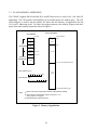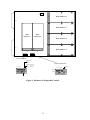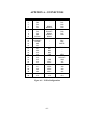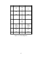
1
VX405C
M/MA Carrier
(408220-0001)
User Manual
Publication No. 11027055 Rev D
Astronics Test Systems Inc.
4 Goodyear, Irvine, CA 92618
Tel: (800) 722-2528, (949) 859-8999; Fax: (949) 859-7139
[email protected] [email protected]
[email protected] http://www.astronicstestsystems.com
Copyright 2009 by Astronics Test Systems Inc. Printed in the United States of America. All rights
reserved. This book or parts thereof may not be reproduced in any form without written permission of the
publisher.
THANK YOU FOR PURCHASING THIS
ASTRONICS TEST SYSTEMS PRODUCT
For this product, or any other Astronics Test Systems product that incorporates
software drivers, you may access our web site to verify and/or download the latest
driver versions. The web address for driver downloads is:
http://www.astronicstestsystems.com/support/downloads
If you have any questions about software driver downloads or our privacy policy, please
contact us at:
[email protected]
WARRANTY STATEMENT
All Astronics Test Systems products are designed to exacting standards and manufactured in
full compliance to our AS9100 Quality Management System processes.
This warranty does not apply to defects resulting from any modification(s) of any product or part
without Astronics Test Systems express written consent, or misuse of any product or part. The
warranty also does not apply to fuses, software, non-rechargeable batteries, damage from
battery leakage, or problems arising from normal wear, such as mechanical relay life, or failure
to follow instructions.
This warranty is in lieu of all other warranties, expressed or implied, including any implied
warranty of merchantability or fitness for a particular use. The remedies provided herein are
buyer’s sole and exclusive remedies.
For the specific terms of your standard warranty, contact Customer Support. Please have the
following information available to facilitate service.
1. Product serial number
2. Product model number
3. Your company and contact information
You may contact Customer Support by:
E-Mail:
[email protected]
Telephone:
+1 800 722 3262
(USA)
Fax:
+1 949 859 7139
(USA)
RETURN OF PRODUCT
Authorization is required from Astronics Test Systems before you send us your product or sub-assembly
for service or calibration. Call or contact Customer Support at 1-800-722-3262 or 1-949-859-8999 or via
fax at 1-949-859-7139. We can also be reached at: [email protected].
If the original packing material is unavailable, ship the product or sub-assembly in an ESD shielding bag
and use appropriate packing materials to surround and protect the product.
PROPRIETARY NOTICE
This document and the technical data herein disclosed, are proprietary to Astronics Test Systems, and
shall not, without express written permission of Astronics Test Systems, be used in whole or in part to
solicit quotations from a competitive source or used for manufacture by anyone other than Astronics Test
Systems. The information herein has been developed at private expense, and may only be used for
operation and maintenance reference purposes or for purposes of engineering evaluation and
incorporation into technical specifications and other documents which specify procurement of products
from Astronics Test Systems.
TRADEMARKS AND SERVICE MARKS
All trademarks and service marks used in this document are the property of their respective owners.
•
Racal Instruments, Talon Instruments, Trig-Tek, ActivATE, Adapt-A-Switch, N-GEN, and PAWS are
trademarks of Astronics Test Systems in the United States.
DISCLAIMER
Buyer acknowledges and agrees that it is responsible for the operation of the goods purchased and
should ensure that they are used properly and in accordance with this document and any other
instructions provided by Seller. Astronics Test Systems products are not specifically designed,
manufactured or intended to be used as parts, assemblies or components in planning, construction,
maintenance or operation of a nuclear facility, or in life support or safety critical applications in which the
failure of the Astronics Test Systems product could create a situation where personal injury or death could
occur. Should Buyer purchase Astronics Test Systems product for such unintended application, Buyer
shall indemnify and hold Astronics Test Systems, its officers, employees, subsidiaries, affiliates and
distributors harmless against all claims arising out of a claim for personal injury or death associated with
such unintended use.
FOR YOUR SAFETY
Before undertaking any troubleshooting, maintenance or exploratory procedure, read carefully
the WARNINGS and CAUTION notices.
This equipment contains voltage hazardous
to human life and safety, and is capable of
inflicting personal injury.
If this instrument is to be powered from the AC line (mains) through an
autotransformer, ensure the common connector is connected to the neutral
(earth pole) of the power supply.
Before operating the unit, ensure the conductor (green wire) is connected to the
ground (earth) conductor of the power outlet. Do not use a two-conductor
extension cord or a three-prong/two-prong adapter. This will defeat the protective
feature of the third conductor in the power cord.
Maintenance and calibration procedures sometimes call for operation of the unit
with power applied and protective covers removed. Read the procedures and
heed warnings to avoid “live” circuit points.
Before operating this instrument:
1. Ensure the proper fuse is in place for the power source to operate.
2. Ensure all other devices connected to or in proximity to this instrument are properly
grounded or connected to the protective third-wire earth ground.
If the instrument:
-
fails to operate satisfactorily
shows visible damage
has been stored under unfavorable conditions
has sustained stress
Do not operate until performance is checked by qualified personnel.
TABLE OF CONTENTS
1.
GENERAL DESCRIPTION ................................................................................................... 1
1.1
PURPOSE OF EQUIPMENT ......................................................................................... 1
1.2
SPECIFICATIONS OF EQUIPMENT ........................................................................... 1
1.2.1
1.2.2
1.2.3
1.2.4
1.2.5
1.2.6
Key Specifications..................................................................................................................................1
Electrical ................................................................................................................................................2
Mechanical .............................................................................................................................................3
Environmental ........................................................................................................................................3
Bus Compliance .....................................................................................................................................3
Applicable Documents ...........................................................................................................................3
2.
INSTALLATION .................................................................................................................... 5
2.1
UNPACKING AND INSPECTION ............................................................................... 5
2.2
HANDLING PRECAUTIONS ....................................................................................... 5
2.3
INSTALLATION OF M/MA MODULES...................................................................... 5
2.4
INSTALLATION OF VX405C CARRIER .................................................................... 7
2.5
PREPARATION FOR RESHIPMENT .......................................................................... 7
3.
FUNCTIONAL DESCRIPTION............................................................................................. 9
3.1
GENERAL ...................................................................................................................... 9
3.2
INTERFACES................................................................................................................. 9
3.3
I/O AND MEMORY ADDRESSING........................................................................... 10
3.4
Triggers ......................................................................................................................... 11
3.5
INTERRUPTS............................................................................................................... 11
3.6
HARDWARE CONFIGURATION .............................................................................. 11
3.7
INDICATORS ............................................................................................................... 13
3.8
CONNECTORS ............................................................................................................ 13
3.8.1
3.8.2
3.8.3
3.9
3.9.1
3.9.2
4.
CONFIGURATION REGISTERS ................................................................................ 14
VXI Configuration Registers................................................................................................................14
Special Function Registers ...................................................................................................................17
OPERATING INSTRUCTIONS........................................................................................... 18
4.1
GENERAL .................................................................................................................... 18
4.2
HARDWARE CONFIGURATION .............................................................................. 18
4.2.1
4.2.2
4.2.3
4.3
4.3.1
4.3.2
4.3.3
4.4
5.
Front Panel Connector..........................................................................................................................13
Rear Connectors ...................................................................................................................................13
+/-24V Auxiliary Connector ................................................................................................................13
Logical Address Selection ....................................................................................................................18
Address Space Selection ......................................................................................................................19
M/MA Module Enable .........................................................................................................................19
SOFTWARE CONFIGURATION................................................................................ 20
Required Memory Setting ....................................................................................................................20
Triggers ................................................................................................................................................21
Interrupts ..............................................................................................................................................21
M/MA Module identification ........................................................................................ 22
TROUBLE ANALYSIS ........................................................................................................ 25
5.1
BUILT IN TEST AND DIAGNOSTICS ...................................................................... 25
5.2
TROUBLE ANALYSIS GUIDE .................................................................................. 25
i
APPENDIX A - CONNECTORS ................................................................................................A-1
LIST OF FIGURES
Figure 1.
Figure 2.
Figure 3.
Figure 4.
Figure 5.
Figure 6.
Figure 7.
Figure 8.
M/MA Configuration Diagram........................................................................................ 6
Functional Block Diagram .............................................................................................. 9
Memory Organization ................................................................................................... 10
Hardware Configurable Controls .................................................................................. 12
Front Panel .................................................................................................................... 13
VXI Configuration Registers ......................................................................................... 15
Special Function Registers ............................................................................................ 17
Fuse Location and Values ............................................................................................. 26
LIST OF TABLES
Table I. Fused Level at VXI Connectors ........................................................................................ 2
Table II. Fused Level at M-Module Connectors ............................................................................. 2
Table III. VXI Register Address Map ........................................................................................... 14
Table IV. M/MA Module EEPROM IDENT Words .................................................................... 22
ii
DOCUMENT CHANGE HISTORY
Revision
Date
D
10/26/09
Description of Change
Initial Astronics Test Systems Release
iii
This page was left intentionally blank.
iv
This manual describes the operation and use of the VX405C M/MA Module Carrier (Astronics
Test Systems part number 408220-0001). The module provides electrical and mechanical
support for up to six industry standard M or MA modules (M/MAs).
Contained within this manual are the physical and electrical specifications, installation and
startup procedures, functional description, and configuration and programming guidelines to
adequately use the product.
Software drivers for an installed M/MA module may be provided by the M/MA module
manufacturer. Some drivers may require modification to operate correctly with the installed VXI
interface I/O library and the addressing methodology used by the VX405C. Contact our
Customer Support or Application Engineering department if necessary.
1. GENERAL DESCRIPTION
The VX405C is a single slot, register-based, C-size, VXIbus compatible carrier module that
provides electrical and mechanical support for up to six single M or MA modules (M/MAs).
Each installed M/MA module appears as an independent VXI instrument to the VXI resource
manager. Full VXI and MA-Module triggering and addressing is supported. For a complete list
of M-modules compatible with the VX405C carrier, visit the mezzanine section of
www.groupipc.com, www.mezzanines.org, or www.vita.com.
1.1 PURPOSE OF EQUIPMENT
This module provides a carrier function for a variety of plug-in modules that vary in functionality
from A/D converters, digital input/output, serial interfaces, to memory devices.
1.2 SPECIFICATIONS OF EQUIPMENT
1.2.1 Key Specifications
•
Supports up to six (6) ANSI/VITA 12-1996 compliant single wide M
or MA-modules, or any valid combination of 2, 3, or 4 wide modules
•
Supports extended M-Module functions (MA) such as extended 24-bit
addressing for up to 16 Mbytes of memory, 32-bit data bus, and trigger
signals for synchronization of MA-Modules
•
VXI A16, A24 and A32 addressing supported
•
D8, D16, and D32 accesses supported
•
Individual Logical Addressing of M/MA-modules
•
Isolated, filtered, and fused +5V, +12V, and -12V supplies for each M-module
•
±24V Auxiliary Power Connector (Rev. C or higher assemblies only)
•
Separate Software Programmable Interrupt Levels
1
•
MA-Module TRIGA and TRIGB can be connected to any VXI TTL
Trigger Line through software control
•
M/MA Module data access time < 800ns
•
Front panel EMI shielding
•
Interactive Mezzanine Control software available
1.2.2 Electrical
The VX405C only requires the +5V power from the VXI back plane; however, ±12V may be
required by installed M-modules and ±24V may be required if the auxiliary power connection is
used. The carrier’s peak module current (IPM) for the +5V supply is 1.2 amps. The total
available power and the fused level of each available voltage are shown in Table I. The power
available and the fused level for the M-Module positions are shown in Table II.
For electrical information on individual M/MA’s, please reference each M/MA’s documentation.
The power requirements for each M/MA installed must be added to the VX405C's requirements
for the total module’s requirements.
Table I. Fused Level at VXI Connectors
+5V
7.2A
1.2A
5.0A
8.0A
5.0A
Total Available from VXI Slot 1
Used by VX405C internal logic
-0001 fused level (up to Rev. D) 2
-0001 fused level (Rev. E or higher) 3
-0002 fused level 4
+12V
1.0A
0A
2.5A
2.5A
2.5A
-12V
1.0A
0A
2.5A
2.5A
2.5A
+24V
1.0A
0A
1A
1.5A
1A
-24V
1.0A
0A
1A
1.5A
1A
Notes:
1. The total current used by the VX405C, M-Modules, and auxiliary +/-24V connector should not
exceed these amounts.
2. Rev. D and below -0001 assemblies use power-off resettable fuse. At currents approaching the
fused level, substantial voltage drops may be experienced.
3. Rev. E and higher -0001 assemblies use standard axial PICO style fuses. Very little voltage
drop is experienced even at the fused level.
4. -0002 assemblies use power-off resettable fuses for the power from the VXI connectors.
Table II. Fused Level at M-Module Connectors
Allowed by specification per M-Module position
-0001 fused level per position (up to Rev. D) 1
-0001 fused level per position (Rev. E or higher) 2
-0002 fused level per position
+5V
1A
1.25A
1.5A
2A
+12V
0.2A
0.3A
0.5A
1A
-12V
0.2A
0.3A
0.5A
1A
Notes:
1. Rev. D and below -0001 assemblies use power-off resettable fuse. At
currents approaching the fused level, substantial voltage drops may be
experienced.
2
2. Rev. E and higher -0001 assemblies use standard axial PICO style fuses.
Very little voltage drop is experienced even at the fused level.
3. -0002 assemblies use standard axial PICO style fuses for the power from the
M-Module connector power.
1.2.3 Mechanical
The mechanical dimensions of the module are in conformance with the VXIbus specification
Rev. 1.4 for single slot 'C' size modules. The nominal dimensions are 233.35 mm (9.187 in) high
x 340 mm (13.386 in) deep.
1.2.4 Environmental
The environmental specifications of the module are:
Operating Temperature:
Storage Temperature:
Humidity:
0°C to +55°C
-40°C to +75°C
<95% without condensation
Installed M/MAs may differ in environmental specification. Refer to each individual M/MA’s
documentation for information.
1.2.5 Bus Compliance
The module complies with the VXIbus Specification Revision 1.4 for C-size register based
modules and with VMEbus Specification ANSI/IEEE STD 1014-1987, IEC 821.
Manufacturer ID:
Model Code:
VXI Access Type:
VXI Addressing:
VXI Data Transfer:
VXI Sysfail:
VXI Interrupts:
VXI Local Bus:
TTL Triggers
Memory Requirements:
M/MA-Module Compliance:
FC116 or VXI-IDENT value
FF216 or VXI-IDENT value
Register Based
A16/A24/A32
D8/D16/D32
supported
ROAK or RORA, programmable levels
not used
SYNC trigger protocol supported
M/MA dependent, up to 16Mbytes (VXI 32Mbytes)
M-Module, MA-Module, A08, A24, D08, D16, D32,
INTA, INTB, INTC, TRIGI, TRIGO, IDENT
1.2.6 Applicable Documents
ANSI/VITA 12-1996 American National Standard for The Mezzanine Concept
M-Module Specification, Approved May 20, 1997
VMEbus International Trade Association
7825 E. Gelding Dr. Suite 104 Scottsdale, AZ 85260-3415
E-mail: [email protected] URL: http:\www.vita.com
3
This page was left intentionally blank.
4
2. INSTALLATION
2.1 UNPACKING AND INSPECTION
Verify that there has been no damage to the shipping container. If damage exists, retain the
container, as it will provide evidence of carrier caused problems. Such problems should be
reported to the shipping courier immediately, as well as to Customer Support. (Contact
information is available in the front few pages of this manual.) If there is no damage to the
shipping container, carefully remove the module from its box and anti-static bag and inspect for
any signs of physical damage. If damage exists, report immediately to Customer Support.
2.2 HANDLING PRECAUTIONS
The VX405C contains components that are sensitive to electrostatic discharge. When handling
the module for any reason, do so at a static-controlled workstation, whenever possible. At a
minimum, avoid work areas that are potential static sources, such as carpeted areas. Avoid
unnecessary contact with the components on the module.
2.3 INSTALLATION OF M/MA MODULES
M/MA modules must be installed before the VX405C is installed into the VXI system. To install
modules, remove the VX405C’s top shield and front panel covers as needed. There is never a
need to remove the VX405C’s bottom shield. Install M/MAs by firmly pressing the connector
on the M/MA together with the connector on the carrier. Secure the M/MA through the holes in
the bottom shield using screws provided with the M/MA. For installing M/MA modules in
locations E or F, longer screws are provided (if necessary) to accommodate the standoffs required
on the VX405C in those locations.
WARNING: The VX405C supports MA-Modules that use three row
interface connectors.
M-Modules use only two rows
connectors and must be correctly positioned to use rows A
and B on the carrier. When using M-Modules, row C on the
VX405C is left unconnected.
There are six possible mounting locations on the carrier: A, B, C, D, E, and F. M/MA modules
may be installed into any of the six locations. Locations A, B, C, and D provide direct access to
the M/MA I/O connector through the front panel. M/MAs that do not require front panel access
(i.e., memory or processing modules) can be easily used in locations E and F. If M/MAs in
locations E and F require front panel access, location D must be left unoccupied to allow cable
routing to locations E and F. Insert the three provided connector covers on location D connector
pins to protect cabling to locations E and F. Use cable guides and tie downs provided to secure
cabling. Configuration is illustrated in Figure 1.
5
CONFIGURATION FOR FOUR (4) M/MA MODULES WITH FRONT PANEL ACCESS
ABC
1
C
B
A
1
20
20
1
M/MA Module A
P1
20
1
M/MA Module E
M/MA Module B
M/MA Module F
20
1
M/MA Module C
20
1
P2
M/MA Module D
20
ABC
CONFIGURATION FOR FIVE (5) M/MA MODULES WITH FRONT PANEL ACCESS
ABC
1
C
B
A
M/MA Module A
1
20
20
1
P1
20
1
M/MA Module E
M/MA Module B
M/MA Module F
20
1
M/MA Module C
20
P2
M/MA Module D
USE CONNECTOR COVERS HERE
ABC
Figure 1. M/MA Configuration Diagram
6
CAUTION: M/MA-Module connectors are NOT keyed. Use extra caution
to avoid misalignment. Applying power to a misaligned
module can damage the M/MA-Module and carrier.
2.4 INSTALLATION OF VX405C CARRIER
CAUTION: Read the entire User's Manual before proceeding with the
installation and application of power.
Set the module's logical address and addressing mode as described in Section 4.2.1 and 4.2.2.
Insert the module into the appropriate slot according to the desired priority. Apply power. If no
obvious problems exist, proceed to communicate with the module as outlined in Section 4.
2.5 PREPARATION FOR RESHIPMENT
If the module is to be shipped separately it should be enclosed in a suitable water and vapor proof
anti-static bag. Heat seal or tape the bag to insure a moisture-proof closure. When sealing the
bag, keep trapped air volume to a minimum.
The shipping container should be a rigid box of sufficient size and strength to protect the
equipment from damage. If the module was received separately from a system, then the original
module shipping container and packing material may be re-used if it is still in good condition.
7
This page was left intentionally blank.
8
3. FUNCTIONAL DESCRIPTION
3.1 GENERAL
The VX405C carrier provides a mechanical and electrical interface between a VXIbus system
and up to six ANSI/VITA 12-1996 standard M/MA modules. The carrier provides VXI register
configuration and access to the M/MA module’s I/O Space and Memory (if present). Each
M/MA is controlled separately and appears as a different logical address in the VXI environment.
A simplified block diagram of the module is shown in Figure 2. The VX405C has no logical
address or programmable registers associated with it, thus allowing the carrier to be completely
transparent in the VXI system.
Front
Panel
VXI I/F
I/F & VXI
Registers
M/MA
Module
E
M/MA
Module
F
I/F & VXI
Registers
I/F & VXI
Registers
I/F & VXI
Registers
I/F & VXI
Registers
I/F & VXI
Registers
M/MA
Module
A
M/MA
Module
B
M/MA
Module
C
M/MA
Module
D
Figure 2. Functional Block Diagram
3.2 INTERFACES
The six M/MA locations interface electrically and mechanically with industry standard M/MA
modules meeting the ANSI/VITA 12-1996 M-Module Specification (approved May 20, 1997).
Each M/MA has its own I/O connector and is accessible through the front panel of the VX405C
via the connector or a user provided cable.
9
3.3 I/O AND MEMORY ADDRESSING
The VX405C supports D8 (Even/Odd), D16, and D32 data access as well as A16, A24, and A32
addressing. The VXI registers of the M/MAs are accessible in the A16 address space. The VXI
Offset Register is used to map the M/MA I/O Space and MA Memory (if applicable) into the
A24 or A32 addressing space. For MA's that support memory, the memory begins at the midpoint of the total memory required as shown in Figure 3.
A24/A32 ADDRESS
A16 ADDRESS
BASE ADDRESS +
VXI ADDR
15
00
VXI
ID
VXI
REGISTERS
15
0
VXI
DEVICE TYPE
02
VXI
STAT/CNTL
04
VXI
06
0
I/O
0000
SPACE
0100
OFFSET
08 (or 20)
UNUSED
INTERRUPT
0A (or 22)
CONTROL
REGISTERS
TRIGGER
0C
UNUSED
HALF OF VXI REQ'D MEM SETTING
3F
BASE ADDRESS (A24) =
M/MA
VXI OFFSET
0
0
HEX
0
0
0
MEMORY
BASE ADDRESS (A32) =
VXI OFFSET
0
HEX
VXI REQUIRED MEM SETTING
Notes:
1) Refer to VXI Device register (02) for details on Req'd Memory Setting
2) AAA bit of the VXI STAT/CNTL register must set to a '1' to
access memory or I/O space.
3) Byte Addressing is referenced above.
Figure 3. Memory Organization
10
3.4 TRIGGERS
Each M/MA is allowed two trigger lines, TRIGA and TRIGB. Triggers may be input or output.
The VX405C Carrier provides software programmable connection to any VXI TTL Trigger line
(SYNC Protocol). Each M/MA trigger can be enabled, logically inverted, configured as input or
output, and mapped to any of the eight VXI TTL Trigger lines.
3.5 INTERRUPTS
Each M/MA can support one interrupt request as specified in the ANSI/VITA 12-1996
Specification. Each interrupt can be programmed to an individual interrupt level and is handled
separately during interrupt acknowledge cycles. A hardware priority for each interrupt
programmed to the same level, begins with M/MA slot A's interrupt being the highest priority
and M/MA slot F's Interrupt being the lowest priority. For further detail, refer to Section 4.3.3.
3.6 HARDWARE CONFIGURATION
The logical address, address space, and positions of the occupied M/MA-module locations must
be configured prior to installing the carrier into the chassis. The configuration is done using the
switches described below and shown in Figure 4.
Logical Address Each M/MA location has its own logical address based on a five position
address switch. The selected logical address establishes the address for position A. The other
positions follow in sequential or modulo-8 order, depending on the Modulo Select switch. See
Section 4.2.1 for more details.
Modulo Select This switch allows the user to set the desired numbering (sequential or modulo-8)
of the logical addresses assigned to each M/MA location on the VX405C. The switch is located
at position 7 of the logical address switch. For further details, refer to Section 4.2.1.
Address Space This switch selects either A24 or A32 addressing. The switch is located at
position 8 of the logical address switch. For A24 addressing the switch should be set in the
OPEN or '1' position.
M/MA Module Enable Six switches are provided to enable the individual M/MA locations. Each
switch corresponds to an M/MA location and must be enabled before the carrier will recognize
an M/MA present.
11
+24V
-24V
GND
D
M/MA MODULE D
C
M/MA MODULE C
B
M/MA MODULE B
A
M/MA MODULE A
P2
M/MA
MODULE F
M/MA
MODULE E
P1
F
E
LOGICAL ADDRESS
Modulo Select
Up = 1
Down = 8
M/MA ENABLE/DISABLE
128
64
32
16
8
Address Space Select
Up =
A16/A24
Down = A16/A32
Reserved
A B C D E F
OPEN
OPEN
1
DISABLE
0
1
2
3
4
5
6
7
ENABLE
8
1
2
3
Not Used
Figure 4. Hardware Configurable Controls
12
4
5
6
7
8
3.7 INDICATORS
Eight LED indicators are provided on the front panel. Their functions are:
VX405C
FAIL:
ID
ID:
FAIL
This front panel LED indicates the PASS/FAIL
(SYSFAIL) status. The LED illuminates
during reset, initialization, or if there is a
failure on the VX405C Carrier itself.
This front panel LED illuminates whenever the host
processor applies the MODID signal to the
slot the module is occupying.
A
A, B, C, D, E, F: These front panel LEDs illuminate whenever
that M/MA is properly accessed by the host
processor.
B
C
D
E
F
3.8 CONNECTORS
3.8.1 Front Panel Connector
The front panel connectors come directly from the M/MAs themselves,
therefore they are M/MA dependent. Front panel covers are provided to
close front panel openings on any unused M/MA locations. The covers
should be used to control airflow and EMI leakage when there is no M/MA
module installed.
3.8.2 Rear Connectors
M/MA CARRIER
VXI
bus
The P1 and P2 connectors are configured in accordance with the VXI
specification. (See APPENDIX A)
3.8.3 +/-24V Auxiliary Connector
The auxiliary +/-24V connector is shown in Figure 4. (1A max. on each)
Figure 5. Front Panel
13
3.9 CONFIGURATION REGISTERS
There are a variety of registers used to configure and control the VX405C module. The VXI
configuration registers provide for control and status as required by the VXIbus specification. An
address map of the registers is shown in Table III.
Table III. VXI Register Address Map
A16 Address
Base + 00
Base + 02
Base + 04
Base + 06
Base + 08 (or 20)
Base + 0A (or 22)
Register Description
VXI ID
VXI Device Type
VXI Status/Control
VXI Offset Register
Interrupt Control Register
Trigger Control Register
3.9.1 VXI Configuration Registers
The VXI configuration registers contain basic information needed to configure a VXIbus system.
The configuration information includes: manufacturer identification, product model code, device
type, memory requirements, device status, and device control. The registers are briefly described
below and are detailed in Figure 6.
VXI Identification (ID) Register (Base + 0016) This read-only register provides the manufacturer
identification, device classification (i.e., register based), and the addressing mode (i.e. A32).
VXI Device Type Register (Base + 0216) This read/write register provides the model code (see
note) identifier and allows the user to set the M/MA's required memory.
Note: The manufacturer and model code identification depends on the installed M/MA-Module’s support
of the VXI extension to the optional M-Module IDENT function. For modules that support the VXI
IDENT extension (non-standard), the manufacturer and model code of the M/MA-Module is reported
and the required memory is automatically set according to the M/MA-Module requirements. For all
other modules, C & H Technologies (FC116) is reported as the manufacturer and the VX405C (FF216)
as the model code. Additionally, the user may have to set the required memory. Refer to M/MA
Module identification for details on the VXI INDENT Extension.
VXI Status/Control Register (Base + 0416) A read of this register provides the state of the P2
MODID* line and the SYSFAIL inhibit, ready and self-test status. A write to this register allows
disabling of the SYSFAIL function and individual reset of the associated M/MA module.
VXI Offset Register (Base + 0616) This read/write register controls the offset value for addressing
the M/MA I/O space and memory. The VXI system resource manager or control module sets this
value according to the memory requirements specified for this module and the memory
requirements of the other instruments in the system.
14
VXI ID
00
Bit
Read
Only
15
14
Device
Class
13
12
11
10
9
8
7
Address
Space
6
5
4
3
2
1
0
Manufacturer ID
Device Class ⇒ Device Class (11 = Register Based)
Address Space ⇒ Address Space (00 = A16/A24, 01 = A16/A32, 10 = reserved, 11 = A16 Only)
Manuf. ID ⇒ Manufacturer Identification (see text for details)
VXI Device Type
02
Bit
Write
Read
15
14
13
12
11
10
9
8
7
6
5
4
3
2
1
Required Memory
Required Memory
Model Code
Model Code ⇒ Model code (see text for details)
Required Memory ⇒ Required memory (value depends on memory required by M/MA module
and VXI address space setting, see table below)
Mem Rq'd by M/MA
A32 Address Space
0 bytes
128 bytes
256 bytes
512 bytes
1K
2K
4K
8K
16K
32K
64K
128K
256K
512K
1M
2M
4M
8M
16M
F (64K)
F (64K)
F (64K)
F (64K)
F (64K)
F (64K)
F (64K)
F (64K)
F (64K)
F (64K)
E (128K)
D (256K)
C (512K)
B (1M)
A (2M)
9 (4M)
8 (8M)
7 (16M)
6 (32M)
A24 Address Space
Figure 6. VXI Configuration Registers
15
E (512 bytes)
E (512 bytes)
E (512 bytes)
D (1K)
C (2K)
B (4K)
A (8K)
9 (16K)
8 (32K)
7 (64K)
6 (128K)
5 (256K)
4 (512K)
3 (1M)
2 (2M)
1 (4M)
0 (8M)
-
0
VXI Status/Control
04
Bit 15
14
13
Write AAA
Read AAA MID CSE
12
11
10
9
8
7
6
5
4
3
1
1
1
1
1
1
1
1
1
1
1
1
1
1
1
1
1
1
-
2
RDY Pass
1
SI
0
0
RST
0
AAA ⇒ A24/A32 Access (0 = disabled)
MID ⇒ Module ID Status (0 = P2 MODID* line is selected)
CSE ⇒ Check Sum Error. ( 0 = error reading non-volatile memory during power-up. Reset
on read, 1 = OK)
RDY ⇒ Ready (1 = ready)
Pass ⇒ Pass/fail indicator (0 = executing or failed, 1 = passed)
SI ⇒ Sysfail Inhibit (1 = inhibit, see note)
RST ⇒ Reset (writing a '1' to this bit resets the M module; after a minimum of 100 µs a ‘0’
must be written to resume normal operation)
Note: The Sysfail Inhibit is a VXI slot inhibit; therefore setting the inhibit bit on any M/MA module will
inhibit SYSFAIL on all M/MA modules.
VXI Offset Register
06
Bit
Write
Read
15
14
13
12
11
10
9
8
7
6
5
4
3
2
Offset Value
Offset Value
Offset Value ⇒ Offset to M/MA's I/O Space and Memory (if applicable)
Figure 6. VXI Configuration Registers (continued)
16
1
0
3.9.2 Special Function Registers
Interrupt Control Register (base + 0816 or base + 2016) This read/write register sets the interrupt
level, and provides the upper byte of vector for M/MA interrupt types INTA and INTB.
Trigger Control Register (base + 0A16 or base + 2216) This read/write register selects a VXI TTL
Trigger line for the TRIGA and TRIGB functions, and sets them as input or output using the VXI
TTLTRG Synchronous (SYNC) Trigger Protocol.
Interrupt Control Register
08
Bit
Write
Read
15
14
13
12
11
10
9
8
Interrupt Vector
Interrupt Vector
7
6
5
4
3
-
-
IDC
IDC
IT
IT
IVE
IVE
2
1
0
Interrupt Level
Interrupt Level
Interrupt Vector ⇒ Upper 8 bits of the interrupt vector for type INTA and INTB interrupts. Default = 0.
IDC ⇒ Interrupt DTACK Control (0 = wait for response from M-module during IACK
cycle, 1 = ignore response from M-module during IACK cycle) Default = 0
IT ⇒ Interrupt Type (0 = follows interrupt type used by installed M-Module, 1 = ROAK
regardless of M-Module interrupt type) Default = 0
Interrupt Level ⇒ Interrupt Level for the M/MA interrupt. Level of '0' disables the interrupt.
Default = disabled.
IVE ⇒ Interrupt vector enable (0 = returns the interrupt vector programmed in this register,
1 = returns the M-module vector, if supported by the M-module). Default = 1.
Trigger Control Register
0A
Bit 15
14
13
Write BEN BDIR BINV
Read BEN BDIR BINV
12
11
-
-
10
9
8
Trig B TTL Sel
Trig B TTL Sel
7
6
5
AEN ADIR AINV
AEN ADIR AINV
4
3
-
-
2
1
0
Trig A TTL Sel
Trig A TTL Sel
AEN ⇒ Trigger enable for Trig A (1 = enable, 0= disable). Default = disable.
ADIR ⇒ Trigger direction for Trig A (0 = input (VXI to M-Module), 1 = output (M-Module
to VXI)). Default = input.
AINV ⇒ Trig A invert bit. (1 = invert logical level of input or output trigger A). Default = 0,
non-inverting.
Trig A TTL Sel ⇒ Trigger A Mapping to VXI TTL Trigger lines 0 -7. Default = 0.
BEN ⇒ Trigger enable for Trig B (1 = enable, 0= disable). Default = disable.
BDIR ⇒ Trigger direction for Trig B (0 = input (VXI to M-Module), 1 = output (M-Module
to VXI)). Default = input.
BINV ⇒ Trig B invert bit. (1 = invert logical level of input or output trigger B). Default = 0,
non-inverting.
Trig B TTL Sel ⇒ Trigger B Mapping to VXI TTL Trigger lines 0 -7. Default = 0.
Figure 7. Special Function Registers
17
4. OPERATING INSTRUCTIONS
4.1 GENERAL
The VX405C is configured through a series of hardware switches and software controlled
registers as below. The switches enable the M/MA slots and configure the logical addresses of
the M/MAs. The VX405C has software controlled registers for each module. These registers
provide configuration of interrupts, triggers, A24/A32 addressing, and required memory. All
other M/MA controls are dependent on a specific M/MA and reside on that module (in I/O and
memory space).
4.2 HARDWARE CONFIGURATION
CAUTION: All hardware configurations must be done only while the
power to the module is OFF.
4.2.1 Logical Address Selection
The logical address is set for each M/MA module by selecting the starting logical address and the
desired sequencing (sequential or multiple of 8) of addressing using the toggle switches provided
on the carrier. With sequential logical addressing (Modulo Select switch in the Up position), the
starting logical address can be selected as any multiple of 8 (i.e., 8, 16, ..., or 248). The M/MA in
location A is assigned the starting logical address and the remaining locations (enabled or
disabled) are assigned logical addresses in sequential order (i.e., 8, 9, 10, etc.). With Modulo-8
logical addressing (Modulo Select switch in the Down position), the starting logical address can
be selected as any multiple of 64 (i.e., 64, 128, or 192). The M/MA in location A is assigned the
starting logical address and the remaining locations (enable or disabled) are assigned logical
addresses in multiples of eight (i.e., 64, 72, 80, etc.). A disabled M/MA location is still counted
when determining the logical address of the enabled locations; however, the disabled location
will not respond when queried by the resource manager and the logical address can be used
elsewhere in the system.
Care should be taken to ensure that none of the modules have the same logical address as another
module in the VXI system. Position 1 on the switch is the most significant bit and has a
weighted value of 128 when the switch is in the OPEN position. Position 5 on the switch is the
least significant bit and has a weighted value of 8 when the switch is in the OPEN position. It is
important to note that if the modulo select switch is set to ‘8’ (the DOWN position), only logical
address switch settings of 64, 128, 192 are valid. The sum of the weighted values of all the
switches in the OPEN position, along with the values in the table below, give the M/MAs' logical
address.
18
Example of sequential addressing:
STARTING
LOGICAL
ADDRESS
Example of Modulo-8 addressing:
STARTING
LOGICAL
ADDRESS
MODULO
SELECT
MODULO
SELECT
NOT USED
128 64 32 16 8
OPEN
(UP=1)
128 64 32 16 8
OPEN
(DOWN=8)
1
1
0
0
1 2 3 4 5 6 7 8
1 2 3 4 5 6 7 8
With the above switch settings, the starting
logical address is 64 + 16 = 80 and the
logical addresses would be assigned as
follows:
M/MA
Location
A
B
C
D
E
F
Location
Enabled
Yes
Yes
Yes
No
No
Yes
With the above switch settings, the starting
logical address is 64 and the logical
addresses would be assigned as follows:
Assigned
Logical
Address
80
81
82
unassigned
unassigned
85
M/MA
Location
A
B
C
D
E
F
Location
Enabled
Yes
Yes
Yes
No
No
Yes
Assigned
Logical
Address
64
72
80
unassigned
unassigned
104
4.2.2 Address Space Selection
A single switch is provided that selects either VXI A16/A24 or A16/A32 addressing for the
entire carrier. This switch is located in position 8 of the logical address switch. The UP (OPEN)
position of this switch corresponds to A16/A24 and the DOWN position to A16/A32.
4.2.3 M/MA Module Enable
Six switches are provided to enable the individual M/MA locations. Each switch represents an
M/MA location and must be enabled before the carrier will recognize a module as present. These
switches are positions 1 - 6 of the M/MA switch and correspond to M/MA locations A - F
respectively. With the switch in the UP (OPEN) position, the M/MA in that location is disabled.
Conversely, with the switch is in the DOWN position, the M/MA in that location is enabled.
Switch positions 7 & 8 are reserved for test purposes and must be in the DOWN position for
normal operation.
19
4.3 SOFTWARE CONFIGURATION
4.3.1 Required Memory Setting
The amount of memory space allocated for a module by the system resource manager or control
module is specified in the Required Memory field of the VXI Device Type register (0x02). The
default Required Memory setting is the minimum amount allowed by the VXI address space
selected. A24 addressing allows a minimum of 512 bytes and A32 addressing allows a minimum
of 64Kbytes.
Note: In order to access the M/MA-Module IO Space and memory, the AAA bit in the VXI
Status/Control register (0x04) must be set high. This is usually done by the resource manager
after allocating memory.
For M-Modules that have only IO Space (256 bytes), the default Required Memory setting is
sufficient and no changes to this field are required.
For MA-Modules that have on-board memory, the Required Memory field must be changed to
cause the resource manager to allocate enough memory space for the IO Space and memory
contained on the MA-Module. Since the VX405C maps a MA-Module’s IO Space into the
lowers 256 bytes of the allocated memory space and the MA-Module’s memory into the upper
half of the allocated memory space, the VXI Required Memory must be set to twice the MAModules required memory.
For example, if an MA-Module has 512Kbytes of on-board memory, then 1Mbyte of VXI memory space
must be allocated. The modules 256 bytes of IO Space is mapped starting at the Offset + 0x000000 (A24)
and the 512Kbytes of memory begins at the Offset + 0x080000 (A24). Proper settings are given in the table
provided under the VXI Device Type register description in Figure 6.
To change the Require Memory field, simply write the new value to VXI Device Type register.
The Model Code bits are ignored. The new setting is stored in non-volatile memory and will
remain the set value until it is changed again. When the required memory bits are written, the
VX405C must be powered off and a resource manager re-ran before the change will take effect.
Due to the required memory setting being stored in non-volatile memory, a short amount of time
is required before the VXI Device Type Register can be accessed again after a write. During this
time, the VXI Ready Bit is cleared in the VXI Status/Control Register (0x04), and then set back to
'1' when access to the VXI Device Type Register is permitted.
Note: If the installed M/MA-Module supports the VXI IDENT extension (non-standard) to the
optional M-Module IDENT function, the required memory is automatically set according to the
M/MA-Module requirements. Refer to M/MA Module identification for details on the VXI
IDENT Extension.
20
4.3.2 Triggers
If the TRIGI or TRIGO functions are supported by an M/MA, any of the eight VXI TTL Trigger
lines can be connected as either an input or output to TRIGA or TRIGB of the M/MA. A
software programmable register (0x0A or 0x22) is provided for each M/MA to connect TRIGA
and TRIGB individually to a VXI TTL Trigger line. Both TRIGA and TRIGB can be
individually enabled and set as input or output as described in Figure 7. An inversion bit is also
provided to allow the user to configure the trigger for a rising or falling edge. All M/MAs on the
carrier can be connected to the same VXI TTL Trigger line to synchronize the M/MAs.
4.3.3 Interrupts
The ANSI/VITA 12-1996 M-Module Specification specifies that an M/MA module may generate
an interrupt. The VXI interrupt level is programmed by writing the desired level into the
Interrupt Level field of the Interrupt Control Register (0x08 or 0x20). Writing a zero to the
Interrupt Level field disables the interrupt for that M/MA.
M/MA modules can support Type A, B, or C interrupts. A Type A interrupter requires software
to access the module to release the interrupt request, sometimes referred to as release on register
access (RORA). A Type B interrupter releases the interrupt request during the hardware interrupt
acknowledge cycle sometimes referred to as release on acknowledge (ROAK). A Type C
interrupter is the same as a Type B interrupter, except the M/MA module also supplies an
interrupt vector during the interrupt acknowledge cycle.
Type A and B interrupters must use the software programmable Interrupt Vector field of the
Interrupt Control Register (0x08) for the upper byte of the VXI interrupt vector (VXI Status/ID)
during the interrupt acknowledge cycle. To enable this action, set the IVE bit to 0 in the Interrupt
Control Register. The lower byte of the interrupt vector is the logical address of the M/MA
module. Type C interrupters provide their own upper byte of the interrupt vector during the
interrupt acknowledge cycle.
The VXI specification recommends that VXI modules use the ROAK interrupt protocol. This
recommendation can be supported by using an M/MA module the uses Type B or Type C
interrupts or by simply setting the interrupt type (IT) bit to a 1 in the Interrupt Control register.
Setting the IT bit to 1 will cause the VX405C to release the VXI interrupt request during the
hardware acknowledge cycle, regardless of the interrupt type used by M/MA module. For Type
A interrupters, the VX405C will release the interrupt request to the VXI during the interrupt
acknowledge cycle, but the interrupt from the M/MA will still be pending until the appropriate
IO register is accessed. The IDC bit may need to be set to a 1 to ignore the response from the Mmodule during the interrupt acknowledge cycle. The VX405C will not issue another interrupt to
the VXI from that M/MA until the M/MA’s interrupt is cleared.
21
4.4 M/MA MODULE IDENTIFICATION
The ANSI/VITA 12-1996 M-Module Specification allows for an optional identification function
called IDENT. This IDENT function provides information about the M/MA module and is
stored in sixteen word deep (32 byte) serial EEPROM. Access is accomplished with read/write
operations on the last address in I/O space and the data is read one bit at a time. Access to the
IDENT is only guaranteed after a reset is performed.
The VX405C also supports the optional VXI-IDENT function introduced by Hewlett-Packard.
This optional function is not part of the approved ANSI/VITA 12-1996 standard. This extension
to the M-module IDENT function increases the size of the EEPROM to at least 64 words (128
bytes) and includes VXI compatible ID and Device Type registers. Details are shown in Table
IV. The VX405C automatically checks the M/MA-Module for support of this optional function
during power-up. If the VX405C detects support, then the VXI Manufacturer ID in the VXI ID
register and the Required Memory and Model Code in the VXI Device Type register are changed
to reflect the settings provided by the M/MA-Module.
Table IV. M/MA Module EEPROM IDENT Words
Word
0
1
2
3
4-7
8-15
16
17
18
19-31
32-63
Description
Sync Code
Module Number
Revision Number
Module Characteristics
Reserved
M-Module Specific
VXI Sync Code
VXI ID
VXI Device Type
Reserved
M-Module Specific
Value (hex)
5346
(Module Dependent)
(Module Dependent)
(Module Dependent)
(Module Dependent)
ACBA
VXI Manufacturer ID
Req’d Mem/Model Code
(Module Dependent)
Note: The VXI Device Type word contains two fields, bits 0-11 are the Model Code and bits 1215 are the Required Memory, where:
Req’d Mem ⇒ 2(23-m), where m is the value of the four bits
Model Code ⇒ manufacturer specified model number
22
This page was left intentionally blank.
23
5. TROUBLE ANALYSIS
5.1 BUILT IN TEST AND DIAGNOSTICS
During power-up initialization, a basic built-in test function is performed. If an initialization
failure is detected, the SYSFAIL lamp will light indicating a failure. Sysfail Inhibit can be used
to help isolate the cause of the failure. The Sysfail Inhibit is a VXI slot inhibit; therefore
setting the inhibit bit on any M/MA module will inhibit SYSFAIL on all M/MA modules.
5.2 TROUBLE ANALYSIS GUIDE
The following is a general guide of the most common problems that may be encountered with the
VX405C, along with a suggestion of the possible causes.
SYMPTOMS
POSSIBLE CAUSES
Bus time out on A16 Access
1. Logical address incorrectly set.
2. Card incorrectly installed.
3. M/MA enable switch not enabled.
4. Logical address Modulo Select switch not set
as expected.
5. Blown fuse (see Figure 8)
Unable to access M/MA memory/IO
space
1. Attempting to access an improper address.
2. VXI memory setting for that M/MA not set to
2 × M/MA’s required memory.
3. AAA bit in the Status/Control register not set
to allow A32/A24 addressing.
4. A24/A32 switch set improperly.
5. Offset register not set correctly.
25
F26
-24V
GND
F21
D
F22
F4
+24V
F25
F16
F3
B
F14
P1
A
E
F11
F
F12
F13
F10
F9
F8
F7
F6
F5
F15
F2
F1
F17
F18
C
F19
F20
P2
Fuse Ref
F1
F2
F3
F4
F5
F6
F7
F8
F9
F10
F11
F12
-0001
2.5A
2.5A
4A
4A
0.5A
0.5A
1.5A
0.5A
0.5A
1.5A
1.5A
0.5A
-0002
SR
SR
SR
SR
1A
1A
2A
1A
1A
2A
2A
1A
Fuse Ref
F13
F14
F15
F16
F17
F18
F19
F20
F21
F22
F25
F26
-0001
0.5A
1.5A
0.5A
0.5A
1.5A
0.5A
0.5A
1.5A
0.5A
0.5A
1.5A
1.5A
-0002
1A
2A
1A
1A
2A
1A
1A
2A
1A
1A
SR
SR
Notes:
1. Table is for -0001 Rev. E assemblies or higher and all revisions of -0002
assemblies.
2. SR = power-off self-resetting fuses
3. All non-SR fuses are miniature PICO II axial fuses rated at 125V or
higher.
Figure 8. Fuse Location and Values
26
APPENDIX A - CONNECTORS
PIN
1
2
3
4
5
6
7
8
9
10
11
12
13
14
15
16
17
18
19
20
21
22
23
24
25
26
27
28
29
30
31
32
C
D08
D09
D10
D11
D12
D13
D14
D15
GND
SYSFAIL*
SYSRESET*
LWORD*
AM5
A23
A22
A21
A20
A19
A18
A17
A16
A15
A14
A13
A12
A11
A10
A09
A08
+12 V
+5 V
B
BG0IN*
BG0OUT*
BG1IN*
BG10UT*
BG2IN*
BG20UT*
BG3IN*
BG3OUT*
AM0
AM1
AM2
AM3
GND
GND
IRQ7*
IRQ6*
IRQ5*
IRQ4*
IRQ3*
IRQ2*
IRQ1*
+5 V
A
D00
D01
D02
D03
D04
D05
D06
D07
GND
DS1*
DS0*
WRITE*
DTACK*
_
_
_
IACK*
IACKIN*
IACKOUT*
AM4
A07
A06
A05
A04
A03
A02
A01
-12 V
+5 V
Figure A-1. P1 Pin Configuration
A-1
PIN
1
2
3
4
5
6
7
8
9
10
11
12
13
14
15
16
17
18
19
20
21
22
23
24
25
26
27
28
29
30
31
32
C
GND
GND
GND
GND
GND
TTLTRG1*
TTLTRG3*
GND
TTLTRG5*
TTLTRG7*
GND
GND
-
B
+5V
GND
A24
A25
A26
A27
A28
A29
A30
A31
GND
+5V
D16
D17
D18
D19
D20
D21
D22
D23
GND
D24
D25
D26
D27
D28
D29
D30
D31
GND
+5V
A
GND
GND
GND
GND
TTLTRG0*
TTLTRG2*
+5V
TTLTRG4*
TTLTRG6*
GND
MODID
GND
-
Figure A-2. P2 Pin Configuration
A-2