1
Agilent TS-5000
Functional Test System
E6198B Switch/Load Unit
User Manual
Agilent Technologies
Notices
© Agilent Technologies, Inc. 2007-2012
Manual Part Number
No part of this manual may be reproduced
in any form or by any means (including
electronic storage and retrieval or translation into a foreign language) without prior
agreement and written consent from Agilent Technologies, Inc. as governed by
United States and international copyright
laws.
E6198-90050
This manual covers the following
Agilent equipment:
• E6198B Switch/Load Unit
• E6175A 8-Channel High Current
Load Card
• E6176A 16-Channel High Current
Load Card
• E6177A 24-Channel Medium Current
Load Card
• U1777A 24-Channel Medium
Current Load Card
• U7178A 8-Channel Heavy Duty Load
Card
• U7179A 16-Channel High Current
Load Card
• E6178B 8-Channel Heavy Duty Load
Card
• N9377A 16-Channel Dual-Load Load
Card
• N9378A 24-Channel Low Resistance
Load Card
• N9379A 48-Channel High Density
Load Card
• E8792A Pin Matrix Card
• E8793A Pin Matrix Card
• E8782A 24-Instrument,
40-Measurement Matrix Card
• E8783A 64-Pin Matrix Card
• E8794A Custom Card
Edition
9th Edition, August 2012
Printed in Malaysia
Agilent Technologies Microwave Products
(Malaysia) Sdn. Bhd.
Bayan Lepas Free Industrial Zone
11900 Penang, Malaysia
Warranty
The material contained in this document is provided “as is,” and is subject to being changed, without notice,
in future editions. Further, to the maximum extent permitted by applicable
law, Agilent disclaims all warranties,
either express or implied, with regard
to this manual and any information
contained herein, including but not
limited to the implied warranties of
merchantability and fitness for a particular purpose. Agilent shall not be
liable for errors or for incidental or
consequential damages in connection
with the furnishing, use, or performance of this document or of any
information contained herein. Should
Agilent and the user have a separate
written agreement with warranty
terms covering the material in this
document that conflict with these
terms, the warranty terms in the separate agreement shall control.
Technology Licenses
The hardware and/or software described
in this document are furnished under a
license and may be used or copied only in
accordance with the terms of such license.
Restricted Rights Legend
If software is for use in the performance of
a U.S. Government prime contract or subcontract, Software is delivered and
licensed as “Commercial computer software” as defined in DFAR 252.227-7014
(June 1995), or as a “commercial item” as
defined in FAR 2.101(a) or as “Restricted
computer software” as defined in FAR
52.227-19 (June 1987) or any equivalent
agency regulation or contract clause. Use,
duplication or disclosure of Software is
subject to Agilent Technologies’ standard
commercial license terms, and non-DOD
Departments and Agencies of the U.S.
Government will receive no greater than
Restricted Rights as defined in FAR
52.227-19(c)(1-2) (June 1987). U.S. Government users will receive no greater than
Limited Rights as defined in FAR 52.227-14
(June 1987) or DFAR 252.227-7015 (b)(2)
(November 1995), as applicable in any
technical data.
Safety Notices
CAUTION
A CAUTION notice denotes a hazard. It calls attention to an operating procedure, practice, or the like
that, if not correctly performed or
adhered to, could result in damage
to the product or loss of important
data. Do not proceed beyond a
CAUTION notice until the indicated
conditions are fully understood and
met.
WA R N I N G
A WARNING notice denotes a
hazard. It calls attention to an
operating procedure, practice, or
the like that, if not correctly performed or adhered to, could result
in personal injury or death. Do not
proceed beyond a WARNING
notice until the indicated conditions are fully understood and
met.
Contents
1
Legal Information
Legal Information 1-2
Warranty 1-2
Technology Licenses
1-2
Restricted Rights Legend 1-2
Service and Support
1-3
Agilent on the Web 1-3
Agilent By Phone
1-3
2
Safety and Regulatory Information
Declaration of Conformity
2-2
Safety Information 2-3
Safety Summary
2-3
Safety Notice
2-3
General Safety Information 2-3
Environmental Conditions 2-4
Before Applying Power
2-4
Ground the System 2-5
Fuses
2-5
Operator Safety Information 2-5
Safety Symbols and Regulatory Markings
2-6
End of Life: Waste Electrical and Electronic Equipment (WEEE) Directive
2002/96/EC 2-8
3
Switch/Load Unit and Plug-In Cards
E6198B Standalone/Integrated Switch/Load Unit Rating
Electrical 3-2
Mechanical 3-2
E6198B Standalone Switch/Load Unit Description
USB Interface 3-5
Digital I/O 3-5
Digital Input 3-5
Open Drain Digital Output 3-6
DAC Channels
3-7
+5 Vdc, +12 Vdc, –12 Vdc, Spare Power
3-7
Current Sense 3-7
Power Bus Sense 3-7
Switch/Load Unit Block Diagram 3-7
E6198B Integrated Switch/Load Unit Description
E6198B/E6218A Switch/Load Unit User Manual
3-2
3-3
3-9
iii
Backplane And Breakout Board Connectors and LEDs 3-10
Backplane Connector Name 3-12
Backplane J1, J2 and J3 Connectors
3-13
Breakout Board Connector Name (for E6198B Standalone
option)
3-14
Backplane Connectors
3-15
Backplane LEDs 3-16
J102 Pinouts 3-16
J1 Pinout 3-20
J2 Pinout 3-20
J3 Pinout 3-20
T1-T14 SLU Logic Power Supply Connector
3-21
Differentiating E6198B Standalone Option and System Integrated
Option 3-22
Fuse Ratings
3-24
DC Power Bus Connections
3-24
4
Configuring the Switch/Load Unit
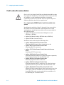
Card Location Recommendations 4-2
Load Card Types and IDS 4-4
Connecting an Additional (Spare) Power Supply
4-5
Configuring the Power Busses
4-6
Setting the UUT Power Supply Remote/Local Sense Jumpers
Configuring the Current-Sense Jumpers
4-10
4-8
Connecting E6198B to the Computer via USB Interface or Parallel
Port
4-12
Adding a Second Switch/Load Unit
Load Box Installation
5
4-13
4-14
Using Load Cards and Loads
Load Card Capabilities
Loads Overview
5-2
5-4
Using the Load Cards
5-5
Load Card Type and Configuration ID
5-5
Using the Agilent E6175A 8-Channel Load Card
5-7
Selecting a Power Supply Configuration
5-9
Selecting a Current-Sense Method
5-10
Installing a LEM Current Transducer 5-11
Selecting and Loading Flyback Protection
5-14
Protection Devices 5-16
iv
E6198B/E6218A Switch/Load Unit User Manual
Selecting a Load Fuse
5-17
Sample Load Configurations
5-17
Setting up a Bridge Configuration
5-19
Connecting Loads
5-20
Load Wiring
5-21
Current Sharing
5-22
UUT Connections
5-23
Using the Agilent E6176A 16-Channel Load Card
5-25
Selecting a Power Supply Configuration
5-27
Selecting a Current-Sense Resistor Value 5-28
Selecting a Load Fuse
5-28
Selecting and Loading Flyback Protection
5-28
Protection Devices 5-30
Connecting Loads
5-32
Load Wiring
5-32
Current Sharing
5-34
External Load Mounting Options 5-35
UUT Connections
5-36
Using the Agilent E6177A 24-Channel Load Card
5-38
Card Layout
5-40
Selecting a Power Supply Configuration 5-41
Using the Power Switches as General Purpose Relays
Connecting Loads
5-42
Load Wiring
5-44
UUT Connections
5-45
5-41
Using the Agilent U7177A 24-Channel Load Card 5-47
Selecting a Power Supply Configuration
5-49
Selecting a Current-Sense Resistor Value 5-50
Using the Power Switches as General Purpose Relays
Connecting Loads
5-51
Load Wiring
5-52
UUT Connections
5-54
5-50
Using the Agilent E6178B 8-Channel Load Card 5-55
Selecting a Power Supply Configuration
5-57
Local / Remote Sensing
5-58
Selecting a Load Fuse
5-58
Current Monitor
5-59
Selecting and Loading Flyback Protection
5-59
Protection Devices 5-60
Load and UUT Connections
5-61
Using the Agilent U7178A 8-Channel Heavy Duty Load Card
E6198B/E6218A Switch/Load Unit User Manual
5-63
v
Selecting a Power Supply Configuration
Local/Remote Sensing
5-66
Selecting a Load Fuse
5-66
Current Monitor
5-66
Selecting and loading flyback protection
Protection Devices 5-68
Load and UUT connections
5-69
5-65
5-67
Using the Agilent U7179A 16-Channel High Current Load Card
Selecting a Power Supply Configuration
5-73
Selecting a Current-Sense Resistor Value 5-74
Selecting a Load Fuse
5-74
Selecting and Loading Flyback Protection
5-74
Protection Devices 5-75
Load Wiring
5-77
External Load Mounting Options 5-79
UUT Connections
5-81
Using the Agilent N9377A 16-Channel Dual-Load Load Card
Selecting a Power Supply Configuration
5-86
Selecting a Current-Sense Resistor Value 5-86
Selecting a Load Fuse
5-86
Selecting and Loading Flyback Protection
5-87
Protection Devices 5-88
Connecting Loads
5-90
Load Wiring
5-90
Recommended Connectors 5-94
Current Sharing
5-95
External Load Mounting Options 5-95
UUT Connections
5-96
5-71
5-83
Using the Agilent N9378A 24-Channel Low Resistance Load Card
5-97
Selecting a Power Supply Configuration 5-100
Using the Power Switches as General Purpose Relays
5-100
Connecting Loads
5-101
Installing and Removing Mezzanine Cards
5-102
Wiring the Mezzanine Cards 5-103
UUT Connections
5-103
Using the Agilent N9379A 48-Channel High-Density Load Card
5-105
Card Layout
5-107
Load Circuit Details 5-109
Selecting a Power Supply Configuration
5-109
Using the Power Switches as General Purpose Relays
5-110
Connecting Loads
5-110
vi
E6198B/E6218A Switch/Load Unit User Manual
6
Using the Pin Matrix Cards
Using the 32-Pin Matrix Cards
6-2
Conceptual Overview 6-2
Features 6-2
Detailed Block Diagram Descriptions
6-3
Differences Between the Cards
6-3
Features Common to Both Cards 6-3
Relay Timer
6-7
Column Disconnect Relay Control 6-7
OAR 6-7
Reset
6-7
Protection Bypass
6-8
Reset State
6-8
User Connectors and Pinouts 6-8
J1 Connector Pinouts 6-9
J1 Instrument Connections
6-11
P2 Connector Pinouts 6-14
Installing in the Switch/Load Unit
6-15
Using the 64-Pin Matrix Cards
6-16
Conceptual Overview 6-16
Features 6-16
Detailed Block Diagram Descriptions
6-17
Differences Between the Cards
6-17
Features Common to Both Cards 6-17
OAR 6-21
Reset
6-21
Protection Bypass
6-21
Reset State
6-22
User Connectors and Pinouts 6-22
J1 Connector Pinouts 6-23
P2 Connector Pinouts 6-27
Installing in the Switch/Load Unit
6-29
7
Using the Custom Card
General-Purpose Breadboard
TS-5430 Series I Emulation
Digital I/O
7-2
7-2
7-2
Connector Breakouts
7-4
J2 Connector Breakouts 7-4
J3/J4 Connector Breakouts (DAC) 7-5
J3 or J4 Connector Breakouts (Event Detector) 7-6
J5 and J6 Connector Breakouts (32-Pin Matrix Cards)
E6198B/E6218A Switch/Load Unit User Manual
7-7
vii
E8794A Components and Schematics
A
7-8
Switch/Load Unit And Card Specifications
Agilent E6198B Switch/Load Unit Specifications
A-2
Agilent E6175A 8-Channel High-Current Load Card Specifications
Agilent E6176A 16-Channel High-Current Load Card Specifications
A-3
A-4
Agilent E6177A 24-Channel Medium-Current Load Card
Specifications A-5
Agilent U7177A 24-Channel Medium-Current Load Card
Specifications A-6
Agilent E6178B 8-Channel Heavy Duty Load Card Specifications
A-7
Agilent U7178A 8-Channel Heavy Duty Load Card Specifications
A-8
Agilent U7179A 16-Channel High Current Load Card Specifications
Agilent N9377A 16-Channel Dual-Load Load Card Specifications
A-9
A-10
Agilent N9378A 24-Channel Low-Resistance Load Card
Specifications A-11
Agilent N9379A 48-Channel High-Density Load Card Specifications
A-12
Agilent E8792A and E8793A Specifications A-13
Instrument Multiplexer (Agilent E8792A Only) A-13
General Specifications (Agilent E8792A and E8793A) A-13
Relay Characteristics (Agilent E8792A and E8793A) A-14
Agilent E8782A and E8783A Specifications A-15
Instrument Multiplexer (Agilent E8782A Only) A-15
General Specifications (Agilent E8782A and E8783A) A-15
Relay Characteristics (Agilent E8782A and E8783A) A-16
Relay Life
A-16
End-of-Life Detection
A-16
Replacement Strategy A-17
B
Register Definitions
Address Space B-2
Base Address
B-3
Switch/Load Unit Register Definitions
B-4
Card Type (R)Base + 0h B-5
Card Configuration (R) Base + 1h B-5
Status Register (R) Base + 2h B-5
Fixture ID (R) Base + 3h B-6
Digital Input (R) Base + 4h B-6
DAC1 Output MSB (W) Base + 8h B-6
viii
E6198B/E6218A Switch/Load Unit User Manual
DAC1 Output LSB (W) Base + 9h B-6
DAC Scaling B-7
Control Register (W) Base + Ah B-7
Open Collector Output (W) Base + Bh
Digital Output (W) Base + Ch B-8
DAC2 Output MSB(W) Base + Dh B-8
DAC2 Output LSB (W) Base + Eh B-9
B-8
Load Card Register Definitions
B-10
Agilent E6175A 8-Channel High-Current Load Card B-11
Agilent E6176A 16-Channel High-Current Load Card
B-15
Agilent E6177A 24-Channel Medium-Current Load Card B-19
Agilent U7177A 24-Channel Medium-Current Load Card With Current
Sense
B-23
Agilent U7178A 8-Channel 40 A Load Card B-28
Agilent U7179A 16-Channel 15 A Load Card B-29
Agilent E6178B 8-Channel 30 Amp Load Card Register
Definitions
B-32
Agilent N9377A 16-Channel Dual-Load Load Card B-34
Agilent N9378A 24-Channel Low-Resistance Load Card B-40
Agilent N9379A 48-Channel High-Density Load Card
B-50
Pin Matrix Card Register Definition B-63
Agilent E8792A and E8793A Pin Card Register Definitions
B-63
Agilent E8782A 24-Instrument, 40-Measurement Matrix Card
B-71
Agilent E8783A 64-Pin Matrix Card
B-80
Agilent E8794A Custom Card Register Definitions
B-89
C
Repair Information
Support Strategy
C-2
Locating Load Card Components C-2
Agilent E6175A 8-Channel High-Current Card
Agilent E6176A 16-Channel High-Current Card
Other Load Cards
C-5
32-Pin Matrix Modules
C-5
64-Pin Matrix Modules
C-8
A
C-2
C-4
Glossary Of Terms
E6198B/E6218A Switch/Load Unit User Manual
ix
THIS PAGE IS INTENTIONALLY LEFT BLANK.
x
E6198B/E6218A Switch/Load Unit User Manual
List of Figures
1
Legal Information
2
Safety and Regulatory Information
3
Switch/Load Unit and Plug-In Cards
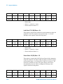
Figure 3-1. Agilent E6198B Standalone Switch/Load Unit Front View 3-4
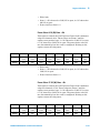
Figure 3-2. Agilent E6198B Standalone Switch/Load Unit Back View 3-4
Figure 3-3. Digital Input Example 3-6
Figure 3-4. Digital Output Example 3-6
Figure 3-5. Switch/Load Unit Block Diagram 3-8
Figure 3-6. E6198B Integrated SLU Back View 3-9
Figure 3-7. Switch/Load Unit Backplane Connectors (USB port adaptor board Not
Shown) 3-10
Figure 3-8. Switch/Load Unit Breakout Board Connectors (Standalone only) 3-11
Figure 3-9. Switch/Load Unit J102 Connector Pinouts 3-17
Figure 3-10. Cable Connector Pinouts 3-18
Figure 3-11. Switch/Load Unit Rear View (Standalone Option) 3-22
Figure 3-12. Switch/Load Unit Rear View (System Integrated Option) 3-23
4
Configuring the Switch/Load Unit
Figure 4-1. Example of Load/Matrix/Custom Cards Loading Order 4-3
Figure 4-2. Component Location/Schematic for User-Installed External Power
Supply 4-5
Figure 4-3. Spare Supply (Input) Connector on SLU rear (SLU standalone) 4-5
Figure 4-4. Power Bus Connectors J801 and J802 4-6
Figure 4-5. Example A: Three Separate Supplies on PB1 - PB4 4-7
Figure 4-6. Example B: Isolated Power Supplies 4-7
Figure 4-7. DC Power Bus Connector Of Standalone SLU 4-8
Figure 4-8. Conceptional View of Local/Remote Sensing 4-9
Figure 4-9. PB Sense Remote/Local Interface (Standalone SLU) 4-10
Figure 4-10. PB Sense Remote/Local and Frame Select Interface (Integrated SLU)
Figure 4-11. ISense Bussed/Split Interface (Standalone SLU) 4-11
Figure 4-12. ISense Bussed/Split Interface (Integrated SLU) 4-11
Figure 4-13. USB Cable Connections 4-12
Figure 4-14. Frame Select Interface (Standalone SLU) 4-13
Figure 4-15. Load Box Installed 4-14
5
4-10
Using Load Cards and Loads
Figure 5-1. Loads/Sources Conceptual Overview 5-4
Figure 5-2. Pin Assignments on the Card Configuration Jack
E6198B/E6218A Switch/Load Unit User Manual
5-5
xi
Figure 5-3. Agilent E6175A 8-Channel High-Current Load Card Block Diagram 5-8
Figure 5-4. Agilent E6175A 8-Channel Load Card Layout 5-9
Figure 5-5. LEM Current Transducer 5-11
Figure 5-6. Component Location for Installing LEM Current Transducer Module 5-12
Figure 5-7. Wiring Options of LEM Model LA25-NP Primary for Various Current
Ranges 5-13
Figure 5-8. 8-Channel Load Card Detail - Flyback Protection Circuit 5-15
Figure 5-9. Agilent E6175A Flyback Protection Polarity 5-15
Figure 5-10. Typical Agilent E6175A Load Card Flyback Protection Circuit 5-16
Figure 5-11. Agilent E6175A Load Examples 5-18
Figure 5-12. Bridge Configuration for Channels 7 and 8 on 8-Channel Load Card 5-19
Figure 5-13. Agilent E6175A Load Mounting Area and CN1/J1 Connectors 5-20
Figure 5-14. Agilent E6175A Load Wiring Schematic and CN1 Pinouts 5-21
Figure 5-15. Agilent E6175A Current Sharing Example 5-22
Figure 5-16. Agilent E6175A 8-Channel High-Current Load Card UUT Connections 5-24
Figure 5-17. Agilent E6176A 16-Channel High-Current Load Card Block Diagram 5-26
Figure 5-18. Agilent E6176A 16-Channel Load Card Layout 5-27
Figure 5-19. 16-Channel Load Card - Flyback Device Polarity Orientation 5-29
Figure 5-20. 16-Channel Load Card - Flyback Circuit Detail 5-30
Figure 5-21. Typical Agilent E6176A Load Card Flyback Protection Circuit 5-31
Figure 5-22. Agilent E6176A Connectors J1/J2 and Mating Connectors CN1/CN2 5-32
Figure 5-23. Agilent E6176A Load Wiring Schematic and CN1/CN2 Pinouts 5-33
Figure 5-24. Agilent E6176A Current Sharing Example 5-34
Figure 5-25. Example: Load Plate with Loads 5-36
Figure 5-26. Agilent E6176A CN2 Connector Pinouts 5-37
Figure 5-27. Agilent E6177A 24-Channel Medium-Current Load Card Block
Diagram 5-39
Figure 5-28. Agilent E6177A 24-Channel Load Card Layout 5-40
Figure 5-29. Using the 24-Channel Load Card Switches as GP Relays 5-42
Figure 5-30. Agilent E6177A Load Mounting Area and CN1/J1 Connectors 5-43
Figure 5-31. Agilent E6177A Load Wiring Schematic and CN1 Pinouts 5-44
Figure 5-32. Agilent E6177A 24-Channel Medium-Current Load Card UUT
Connections 5-46
Figure 5-33. Agilent U7177A 24-Channel Medium-Current Load Card Block
Diagram 5-48
Figure 5-34. The U7177A Layout 5-49
Figure 5-35. Using the 24-Channel Load Card Switches as GP Relays 5-51
Figure 5-36. Agilent U7177A Connector J1 and Mating Connector CN1 5-52
Figure 5-37. Agilent U7177A Load Wiring Schematic and CN1 Pinouts 5-53
Figure 5-38. Agilent U7177A 24-Channel Medium-Current Load Card UUT
Connections 5-54
Figure 5-39. Agilent E6178B 8-Channel Heavy Duty Load Card Block Diagram 5-56
Figure 5-40. Agilent E6178B 8-Channel Heavy Duty Load Card Layout 5-57
Figure 5-41. Typical Agilent E6178B Load Card Flyback Protection Circuit 5-60
xii
E6198B/E6218A Switch/Load Unit User Manual
Figure 5-42. Agilent E6178B Load Card Wiring 5-62
Figure 5-43. Agilent U7178A 8-Channel Heavy Duty Load Card Block Diagram 5-64
Figure 5-44. Agilent U7178A 8-Channel Heavy Duty Load Card Layout 5-65
Figure 5-45. Typical Agilent U7178A load card flyback protection circuit 5-68
Figure 5-46. Agilent U7178A load card wiring 5-70
Figure 5-47. Agilent U7179A 16-Channel High-Current Load Card Block Diagram 5-72
Figure 5-48. Agilent U7179A 16-Channel Load Card Layout 5-73
Figure 5-49. Typical Agilent U7179A Load Card Flyback Protection Circuit 5-76
Figure 5-50. Agilent U7179A Connectors J1/J2 and Mating Connectors CN1/CN2 5-77
Figure 5-51. Agilent U7179A Load Wiring Schematic and CN1/CN2 Pinouts 5-78
Figure 5-52. Agilent U7179A Current Sharing Example 5-79
Figure 5-53. Example: Load Plate with loads 5-80
Figure 5-54. Agilent U7179A CN2 Connector Pinouts 5-82
Figure 5-55. Agilent N9377A 16-Channel Dual-Load Load Card Block Diagram 5-84
Figure 5-56. N9377A 16-Channel Load Card Layout 5-85
Figure 5-57. N9377A Load Card - Flyback Locator and Polarity Orientation 5-87
Figure 5-58. N9377A Load Card - Flyback Circuit Detail 5-88
Figure 5-59. Typical Agilent N9377A Load Card Flyback Protection Circuit 5-89
Figure 5-60. Agilent N9377A Connectors J1/J2 and Mating Connectors J1/J2 5-90
Figure 5-61. N9377A Load Wiring Schematic 5-92
Figure 5-62. J1 and J2 Connector Layout 5-93
Figure 5-63. Agilent N9377A Pinout Table (160-pin option) 5-94
Figure 5-64. Agilent N9377A Current Sharing Example 5-95
Figure 5-65. Agilent N9378 24-Channel Low-Resistance Load Card Block Diagram 5-98
Figure 5-66. Agilent N9378A 24-Channel Load Card Layout 5-99
Figure 5-67. Load circuit details 5-100
Figure 5-68. Agilent N9378A Load Mounting Area and CN1/J1 Connectors 5-102
Figure 5-69. Mezzanine Card Pinouts for N9378A 24-Channel Load Card 5-103
Figure 5-70. Agilent N9378A UUT Connector 5-104
Figure 5-71. Agilent N9379A 48-Channel High-Density Load Card Block Diagram 5-106
Figure 5-72. Agilent N9379A Layout 5-108
Figure 5-73. Load Circuit Details 5-109
Figure 5-74. Agilent N9379A Mezzanine Card 5-110
6
Using the Pin Matrix Cards
Figure 6-1. Pin Matrix Cards Conceptual Overview 6-2
Figure 6-2. Agilent E8792A Detailed Block Diagram 6-5
Figure 6-3. Agilent E8793A Detailed Block Diagram 6-6
Figure 6-4. Column Disconnect and Protection Bypass Relays
Figure 6-5. J1 Pinouts--Instrument and Abus Access 6-10
Figure 6-6. J1 Example Instrument Connections 6-11
Figure 6-7. Instrument BNC Cables 6-12
Figure 6-8. J2 Pinouts--Rear Aux Access 6-13
E6198B/E6218A Switch/Load Unit User Manual
6-8
xiii
Figure 6-9. P2 Pinouts--Row, Aux, and UUT Common Main Access 6-14
Figure 6-10. Installed 32-Pin Matrix Cards 6-15
Figure 6-11. Pin Matrix Cards Conceptual Overview 6-16
Figure 6-12. Agilent E8782A Detailed Block Diagram 6-19
Figure 6-13. Agilent E8783A Detailed Block Diagram 6-20
Figure 6-14. Column Disconnect and Bypass Protection Relays 6-22
Figure 6-15. J1 Pinouts--Instrument and Abus Access 6-23
Figure 6-16. J2 Pinouts--Rear Aux Access for E8782A 6-25
Figure 6-17. J2 Pinouts--Rear Aux Access for E8783A 6-26
Figure 6-18. P2 Pinouts--Row, Aux, and UUT Common Main Access for E8782A
Figure 6-19. P2 Pinouts-Row, Aux, and UUT Common Main Access for E8783A
Figure 6-20. Installed 32-Pin Matrix Cards 6-29
7
Using the Custom Card
Figure 7-1. Custom Card Features 7-3
Figure 7-2. J2 Configuration Lines Pinouts 7-4
Figure 7-3. J3/J4 Breakouts for Agilent E1418 DAC 7-5
Figure 7-4. J3 or J4 Connector Breakouts for Agilent E6174 Event Detector
Figure 7-5. J5 and J6 Breakouts (32-Pin Matrix Cards) 7-7
Figure 7-6. E8794A Layout 7-8
Figure 7-7. E8794A Component Locator 7-9
Figure 7-8. E8794A Schematic 7-10
Figure 7-9. Status and Control Interface 7-11
A
Switch/Load Unit And Card Specifications
B
Register Definitions
Figure B-1. Relay controlled by registers Base+03h-Base+09h
Figure B-2. Mezzanine Card Layout B-42
Figure B-3. Mezzanine Card Layout B-53
C
6-27
6-28
7-6
B-35
Repair Information
Figure C-1. Agilent E6175A Component Locator (Rear View) C-3
Figure C-2. Agilent E6176A 16-Channel Load Card Component Locator (Rear View)
A
xiv
C-4
Glossary Of Terms
E6198B/E6218A Switch/Load Unit User Manual
List of Tables
1
Legal Information
Table 1-1. Agilent Sales And Support Contact Numbers
2
Safety and Regulatory Information
Table 2-1. Environment Requirements 2-4
Table 2-2. Safety Symbols and Regulatory Markings
3
1-3
2-6
Switch/Load Unit and Plug-In Cards
Table 3-1. Switch/Load Unit Rating (Electrical) 3-2
Table 3-2. Switch/Load Unit Rating (Mechanical) 3-2
Table 3-3. Backplane Connectors for E6198B 3-12
Table 3-4. Backplane Factory Default Connector Settings
Table 3-5. Breakout Board Connectors 3-14
Table 3-6. J102 signal definitions 3-19
Table 3-7. Switch/Load Unit J1 Pinout 3-20
Table 3-8. Switch/Load Unit J2 Pinout 3-20
Table 3-9. Switch/Load Unit J3 Pinout 3-20
Table 3-10. Power Supply Input for each Jumpers 3-21
Table 3-11. Fuses Ratings 3-24
4
Configuring the Switch/Load Unit
5
Using Load Cards and Loads
3-13
Table 5-1. Load Card Capabilities 5-2
Table 5-2. Components involved in LEM Module Installation
Table 5-3. CH1 to CH16 flyback protection 5-75
6
Using the Pin Matrix Cards
7
Using the Custom Card
A
Switch/Load Unit And Card Specifications
B
Register Definitions
5-13
Table B-1. Standard Registers B-2
Table B-2. Standard Registers B-2
Table B-3. Switch/Load Unit Registers B-4
Table B-4. DAC Scaling Examples B-7
Table B-5. OCoutx States B-8
Table B-6. Summary of Load Card Register Definitions
E6198B/E6218A Switch/Load Unit User Manual
B-10
xv
C
Repair Information
Table C-1. Measurement Matrix Relays C-5
Table C-2. Instrument Matrix Relays C-7
Table C-3. Bypass and Disconnect Relays C-7
Table C-4. Miscellaneous Relays C-7
Table C-5. Measurement Matrix Relays for E8782A C-8
Table C-6. Measurement Matrix Relays for E8783A C-10
Table C-7. Bypass and Disconnect Relays for E8782A and E8783A
A
xvi
C-12
Glossary Of Terms
E6198B/E6218A Switch/Load Unit User Manual
Agilent TS-5000
E6198B/E6218A Switch/Load Unit User Manual
1
Legal Information
Legal Information 1-2
Warranty 1-2
Technology Licenses 1-2
Restricted Rights Legend 1-2
Service and Support 1-3
Agilent on the Web 1-3
Agilent By Phone 1-3
Agilent Technologies
1-1
1
Legal Information
Legal Information
Warranty
The material contained in this document is provided “as is,” and
is subject to being changed, without notice, in future editions.
Further, to the maximum extent permitted by applicable law,
Agilent disclaims all warranties, either express or implied, with
regard to this manual and any information contained herein,
including but not limited to the implied warranties of
merchantability and fitness for a particular purpose. Agilent
shall not be liable for errors or for incidental or consequential
damages in connection with the furnishing, use, or performance
of this document or of any information contained herein.
Should Agilent and the user have a separate written agreement
with warranty terms covering the material in this document
that conflict with these terms, the warranty terms in the
separate agreement shall control.
Technology Licenses
The hardware and/or software described in this document are
furnished under a license and may be used or copied only in
accordance with the terms of such license.
Restricted Rights Legend
If software is for use in the performance of a U.S. Government
prime contract or subcontract, Software is delivered and
licensed as “Commercial computer software” as defined in
DFAR 252.227-7014 (June 1995), or as a “commercial item” as
defined in FAR 2.101(a) or as “Restricted computer software” as
defined in FAR 52.227-19 (June 1987) or any equivalent agency
regulation or contract clause. Use, duplication or disclosure of
Software is subject to Agilent Technologies’ standard
commercial license terms, and non-DOD Departments and
Agencies of the U.S. Government will receive no greater than
Restricted Rights as defined in FAR 52.227-19(c)(1-2)(June
1987). U.S. Government users will receive no greater than
Limited Rights as defined in FAR 52.227-14 (June 1987) or
DFAR 252.227-7015 (b)(2)(November 1995), as applicable in any
technical data.
1-2
E6198B/E6218A Switch/Load Unit User Manual
Legal Information
1
Service and Support
Any adjustment, maintenance, or repair of this product must be
performed by qualified personnel. Contact your customer
engineer through your local Agilent Technologies Service
Center.
Agilent on the Web
You can find information about technical and professional
services, product support, and equipment repair and service on
the Web: http://www.agilent.com/
Double-click the link to Test & Measurement. Select your country
from the drop-down menus. The Web page that appears next has
contact information specific for your country.
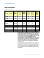
Agilent By Phone
If you do not have access to the Internet, call one of the
numbers in Table 1-1
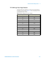
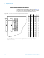
Table 1-1 Agilent Sales And Support Contact Numbers
Americas
Asia Pacific
E6198B/E6218A Switch/Load Unit User Manual
Canada
(877) 894-4414
Latin America
305 269 7500
United States
(800) 829-4444
Australia
1 800 629 485
China
800 810 0189
Hong Kong
800 938 693
India
1 800 112 929
Japan
0120 (421) 345
Korea
080 769 0800
Malaysia
1 800 888 848
Singapore
1 800 375 8100
Taiwan
0800 047 866
Thailand
1 800 226 008
1-3
1
Legal Information
Table 1-1 Agilent Sales And Support Contact Numbers (continued)
Europe & Middle East
Austria
01 36027 71571
Belgium
32 (0) 2 404 93 40
Denmark
45 70 13 15 15
Finland
358 (0) 10 855 2100
France
0825 010 700*
*0.125 €/minute
Germany
07031 464 6333**
**0.14 €/minute
Ireland
1890 924 204
Israel
972-3-9288-504/544
Italy
39 02 92 60 8484
Netherlands
31 (0) 20 547 2111
Spain
34 (91) 631 3300
Sweden
0200-88 22 55
Switzerland
0800 80 53 53
United Kingdom
44 (0) 118 9276201
Other European
Countries:
www.agilent.com/find/
contactus
Manufacturing Address
Agilent Technologies Microwave Products (Malaysia) Sdn. Bhd.
Bayan Lepas Free Industrial Zone,
11900 Penang,
Malaysia.
1-4
E6198B/E6218A Switch/Load Unit User Manual
Agilent TS-5000
E6198B/E6218A Switch/Load Unit User Manual
2
Safety and Regulatory Information
Declaration of Conformity 2-2
Safety Information 2-3
Safety Summary 2-3
Safety Notice 2-3
General Safety Information 2-3
Environmental Conditions 2-4
Before Applying Power 2-4
Ground the System 2-5
Fuses 2-5
Operator Safety Information 2-5
Safety Symbols and Regulatory Markings 2-6
End of Life: Waste Electrical and Electronic Equipment (WEEE)
Directive 2002/96/EC 2-8
Agilent Technologies
2-1
2
Safety and Regulatory Information
Declaration of Conformity
The Declaration of Conformity (DoC) for this product is
available on the Agilent Technologies website. You can search
for the DoC by its product model or description at the following
web address:
http://regulations.corporate.agilent.com/DoC/search.htm
NOTE
2-2
If you are unable to locate the DoC, please contact your local Agilent
representative.
E6198B/E6218A Switch/Load Unit User Manual
2
Safety and Regulatory Information
Safety Information
Safety Summary
The following general safety precautions must be observed
during all phases of operation of this instrument. Failure to
comply with these precautions or with specific warnings
elsewhere in this manual violates safety standards of design,
manufacture, and intended use of the instrument. Agilent
Technologies, Inc. assumes no liability for the customer's failure
to comply with these requirements.
Safety Notice
CAUTION
A CAUTION notice denotes a hazard. It calls attention to an
operating procedure, practice, or the like, that, if not correctly
performed or adhered to, could result in damage to the product or
loss of important data. Do not proceed beyond a CAUTION notice
until the indicated conditions are fully understood and met.
WA RNING
A WARNING notice denotes a hazard. It calls attention to an
operating procedure, practice, or the like that, if not correctly
performed or adhered to, could result in personal injury or death.
Do not proceed beyond a WARNING notice until the indicated
conditions are fully understood and met.
General Safety Information
This product is provided with a protective earth terminal. The
protective features of this product may be impaired if it is used
in a manner not specified in the operation instructions.
WA RNING
DO NOT OPERATE IN AN EXPLOSIVE ATMOSPHERE. Do not
operate the product in the presence of flammable gases or
flames.
E6198B/E6218A Switch/Load Unit User Manual
2-3
2
Safety and Regulatory Information
WA RNING
DO NOT REMOVE RACK PANELS OR INSTRUMENT COVERS.
Operating personnel must not remove any rack panels or
instrument covers. Component replacement and internal
adjustments must be made only by qualified service personnel.
Products that appear damaged or defective should be made
inoperative and secured against unintended operation until they
can be repaired by a qualified service personnel.
WA RNING
The protection provided by the Agilent TS-5000 system may be
impaired if the system is used in a manner not specified by
Agilent.
Environmental Conditions
The Automotive Electronics Functional Test System is designed
for indoor use only. Table 2-1 shows general environmental
requirements.
Table 2-1 Environment Requirements
CAUTION
Environment Conditions
Requirements
Maximum Altitude
2000 meters
Temperature (Operation)
5 °C to 40 °C
Maximum Relative Humidity
The test system is designed to
operate in the range from 5% to 80%
relative humidity (non-condensing).
This product is designed for use in Installation Category II and
Pollution Degree 2, per IEC 61010-1.
Before Applying Power
Verify that the product is set to match the available line voltage
and all safety precautions are taken. Note the external markings
of the instruments described in “Safety Symbols and Regulatory
Markings”.
2-4
E6198B/E6218A Switch/Load Unit User Manual
Safety and Regulatory Information
2
Ground the System
To minimize shock hazard, the instrument chassis and cover
must be connected to an electrical protective earth ground. The
instrument must be connected to the ac power mains through a
grounded power cable, with the ground wire firmly connected
to an electrical ground (safety ground) at the power outlet. Any
interruption of the protective (grounding) conductor or
disconnection of the protective earth terminal will cause a
potential shock hazard that could result in personal injury.
Fuses
Use only fuses with the required rated current, voltage, and
specified type (normal blow, time delay). Do not use repaired
fuses or short-circuited fuse holders. To do so could cause a
shock or fire hazard.
For AC inlet fuse, use only 5A/250 Vac fuse with Time-Lag and
Low Breaking capacity. For other fuse ratings, refer Table 3-11.
In order to avoid electrical hazards, all system internal fuses must
be replaced by trained and qualified personnel.
WA RNING
Operator Safety Information
Module connectors and Test Signal cables connected to them
cannot be operator accessible.
WA RNING
M
Cables and connectors are considered inaccessible if a tool (e.g.
screwdriver, wrench, socket, etc.) or a key (equipment in a
locked cabinet) is required to gain access to a conductive
surface connected to any cable conductor (High, Low or Guard).
WA RNING
Assure the equipment under test has adequate insulation
between the cable connections and any operator-accessible parts
(doors, covers, panels shields, cases, cabinets, etc.)
Verify there are multiple and sufficient protective means (rated
for the voltages you are applying) to assure the operator will
NOT come into contact with any energized conductor even if
one of the protective means fails to work as intended. For
E6198B/E6218A Switch/Load Unit User Manual
2-5
2
Safety and Regulatory Information
example, the inner side of a case, cabinet, door cover or panel
can be covered with an insulating material as well as routing the
test cables to the front panel connectors of the module through
non-conductive, flexible conduit such as that used in electrical
power distribution.
Safety Symbols and Regulatory Markings
Symbols and markings on the system, in manuals and on
instruments alert you to potential risks, provide information
about conditions, and comply with international regulations.
Table 2-2 defines the symbols and markings you may find in a
manual or on an instrument.
Table 2-2 Safety Symbols and Regulatory Markings
Symbols
Description
Safety symbols
Warning: risk of electric shock.
Caution: refer to accompanying documents.
Alternating current.
Both direct and alternating current.
Earth (ground) terminal
Protective earth (ground) terminal
Frame or chassis terminal
Terminal is at earth potential. Used for measurement and
control circuits designed to be operated with one terminal at
earth potential.
Switch setting indicator. O = Off, | = On.
2-6
E6198B/E6218A Switch/Load Unit User Manual
2
Safety and Regulatory Information
Table 2-2 Safety Symbols and Regulatory Markings (continued)
Symbols
Description
Standby (supply); units with this symbol are not completely
disconnected from ac mains when this switch is off. To
completely disconnect the unit from ac mains, either
disconnect the power cord, or have a qualified electrician
install an external switch.
Regulatory markings
This text indicates that the ISM device complies with
Canadian ICES-001.
Cet appareil ISM est conforme à la norme NMB-001 du
Canada.
The CSA mark is a registered trademark of the Canadian
Standards Association. A CSA mark with the indicators “C”
and “US” means that the product is certified for both the
U.S. and Canadian markets, to the applicable American and
Canadian standards.
The C-tick mark is a registered trademark of the Spectrum
Management Agency of Australia. This signifies compliance
with the Australia EMC Framework regulations under the
terms of the Radio Communication Act of 1992.
This instrument complies with the WEEE Directive
(2002/96/EC) marking requirement. This affixed product
label indicates that you must not discard this
electrical/electronic product in domestic household waste.
The CE mark is a registered trademark of the European
Community. This CE mark shows that the product complies
with all the relevant European Legal Directives.
E6198B/E6218A Switch/Load Unit User Manual
2-7
2
Safety and Regulatory Information
End of Life: Waste Electrical and Electronic Equipment (WEEE) Directive
2002/96/EC
This product complies with the WEEE Directive (2002/96/EC)
marking requirement. The affixed product label (see below)
indicates that you must not discard this electrical/electronic
product in domestic household waste.
Product Category:
With reference to the equipment types in the WEEE directive
Annex 1, this product is classified as a “Monitoring and Control
Instrumentation” product.
Do not dispose in domestic household waste
To return unwanted products, contact your local Agilent office,
or see:
http://www.agilent.com/environment/product
for more information.
2-8
E6198B/E6218A Switch/Load Unit User Manual
Agilent TS-5000
E6198B Switch/Load Unit User Manual
3
Switch/Load Unit and Plug-In Cards
E6198B Standalone/Integrated Switch/Load Unit Rating 3-2
E6198B Standalone Switch/Load Unit Description 3-3
E6198B Integrated Switch/Load Unit Description 3-9
Backplane And Breakout Board Connectors and LEDs 3-10
Differentiating E6198B Standalone Option and System Integrated
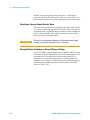
Option 3-22
This chapter gives an overview of the Agilent E6198B
(Standalone and Integrated) Switch/Load Unit (SLU), load
cards, and other associated equipment.
Agilent Technologies
3-1
3
Switch/Load Unit and Plug-In Cards
E6198B Standalone/Integrated Switch/Load Unit Rating
Electrical
Table 3-1 Switch/Load Unit Rating (Electrical)
Parameter
Value
Input Voltage
100–240 VAC nominal
Frequency
50/60 Hz
Power
325 W maximum
Mechanical
Table 3-2 Switch/Load Unit Rating (Mechanical)
3-2
Parameter
Value
Width
484.64 mm
Height
373.61 mm
Depth
520.52 mm
Weight
15.0 kg
E6198B/E6218A Switch/Load Unit User Manual
3
Switch/Load Unit and Plug-In Cards
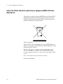
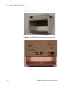
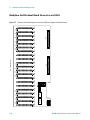
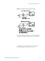
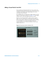
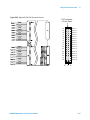
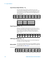
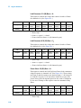
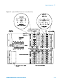
E6198B Standalone Switch/Load Unit Description
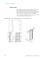
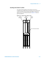
The Switch/Load Unit (Figure 3-1) consists of a standard VME
type enclosure, a custom high current backplane, and slots for
up to 21 optional Agilent plug-in cards. The following plug-in
cards are available:
• Agilent E6175A 8-channel load card
• Agilent E6176A 16-channel load card
• Agilent E6177A 24-channel load card
• Agilent U7177A 24-channel load card with current sense
• Agilent E6178B 8-channel heavy duty load card
• Agilent N9377A 16-channel dual-load load card
• Agilent N9378A 24-channel low resistance load card
• Agilent N9379A 48-channel high-density load card
• Agilent E8792A 32-pin matrix card with instrumentation
support
• Agilent E8793A 32-pin matrix card
• Agilent E8782A 40-pin matrix card with 24 instrumentation
support
• Agilent E8783A 64-pin matrix card
• Agilent E8794A custom card
• Agilent U7178A 8-channel heavy duty load card
• Agilent U7179A 16-channel high current load card
Load cards are described in detail in Chapter 5 and Appendix A
to Appendix C of this manual. The pin matrix cards are
described in Chapter 6. The E8794A custom card is discussed in
Chapter 7.
E6198B/E6218A Switch/Load Unit User Manual
3-3
3
Switch/Load Unit and Plug-In Cards
Figure 3-1 Agilent E6198B Standalone Switch/Load Unit Front View
Figure 3-2 Agilent E6198B Standalone Switch/Load Unit Back View
3-4
E6198B/E6218A Switch/Load Unit User Manual
3
Switch/Load Unit and Plug-In Cards
In addition to holding load cards, pin matrix cards, and custom
cards, the Switch/Load Unit also provides the following
capabilities:
• Built-in USB interface
• Digital I/O
• Current Sense
• Power Bus Sense
• Two DAC Channels
• +5, +12V, –12V, and Spare Power
Each of the above features is described in detail in the following
sections.
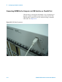
USB Interface
The Switch/Load Unit switching and data transfer is controlled
by a built-in USB interface. Figure 4-13 shows the location of
the USB interface.
Digital I/O
The Switch/Load Unit provides 8-bits of digital input, 8-bits of
digital output (Open Drain Out), and 8-bits of TTL-level digital
output (Spare Digital Out). There is no handshaking capability
in the digital I/O. Typical usage of the digital I/O includes:
• Automation control
• Digital control of circuitry on the Agilent E8794A Custom
Card
• Digital switches (for example, to indicate door open/closed)
• Actuator control
• Fixture ID
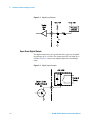
Digital Input
The digital input bits have TTL thresholds (0.55 Vdc for low,
3.0 Vdc for high) and are protected to ±24 Vdc. These includes
the Fixture IDs that also use standard TTL inputs, but are not
protected to ±24 Vdc. Figure 3-3 is a typical example showing
the usage of a digital input bit.
E6198B/E6218A Switch/Load Unit User Manual
3-5
3
Switch/Load Unit and Plug-In Cards
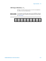
Figure 3-3 Digital Input Example
Open Drain Digital Output
The digital output bits use open drain drive circuitry designed
for pull-ups up to +24 Vdc. The output port FET can sink up to
250 mA. Figure 3-4 shows one digital output bit controlling a
relay.
Figure 3-4 Digital Output Example
3-6
E6198B/E6218A Switch/Load Unit User Manual
3
Switch/Load Unit and Plug-In Cards
DAC Channels
The two 14-bit channels of DAC provide ±16 V at 10 mA each. To
provide this voltage swing, a charge pump is used to step-up the
±12 V supply. The DAC channels are typically used for
controlling differential input, voltage-controlled power supplies.
+5 Vdc, +12 Vdc, –12 Vdc, Spare Power
+5 V, +12 V, and –12V from the Switch/Load Unit Power Supply.
The +5 V supply can deliver 7.5 A to 30 A, +12 V supply can
deliver 2.5 A to 12.5 A, and the –12 V supply can deliver 700 mA
to 1 A. You can also connect an additional (spare) power supply
to the Switch/Load Unit backplane, see “Connecting an
Additional (Spare) Power Supply for details.
NOTE
Power supplies +5 V, +12 V, and –12 V for E6198B have non-resettable
fuses. (Non-resettable fuses need to be replaced, refer to Table 3-11 for
fuse ratings.)
Spare supply has resettable fuse. If an overload occurs, the fuse(s) open.
To reset the fuse(s), remove power from the Switch/Load Unit for
approximately 20 seconds. The fuse(s) reset when power is re-applied.
Current Sense
The Isense+ and Isense– lines sense current on a selected load
card channel. They connect to the current sense bus on the SLU
backplane. Current sense lines of each channel are multiplexed.
Only one channel can connect to the current sense bus at one
time.
Power Bus Sense
Power Bus Sense lines 1-4 remotely sense power supplies
connected to power buses 1-4. This sensing compensates the
losses in the system wiring to ensure that the set voltage is
applied to the sense point.
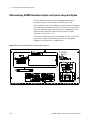
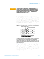
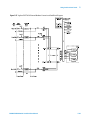
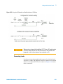
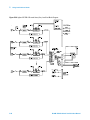
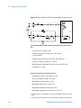
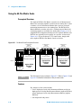
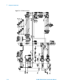
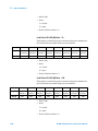
Switch/Load Unit Block Diagram
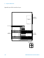
Figure 3-5 shows a block diagram of the SLU. All plug-in cards
are optional so your system will have a different mix of cards
from that shown here. The Test System Interface or Mass
Interconnect are also optional — you can also interface directly
to the Switch/Load Unit. See Chapter 4 for details.
E6198B/E6218A Switch/Load Unit User Manual
3-7
3
Switch/Load Unit and Plug-In Cards
Figure 3-5 Switch/Load Unit Block Diagram
Power
Supply #1
Load Card #1
Power
Supply #2
Pin Matrix Card #1
Power
Supply #3
Custom Card
Analog Bus
Power Bus
Digital In, Power Bus Sense ,
Isense
Switch/Load Unit
Circuitry
Digital Out, DAC, +12V, -12V
Load Card #2
Pin Matrix Card #2
Load Card #n
Test System Interface or Mass Interconnect
Agilent E6198B Switch/Load Unit
To/From
UUT
Pin Matrix Card #n
Note: All plug -in cards are optional --the mix and numbers of cards in your system will be different than shown here
3-8
.
E6198B/E6218A Switch/Load Unit User Manual
Switch/Load Unit and Plug-In Cards
3
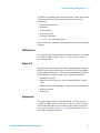
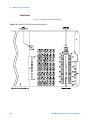
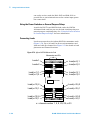
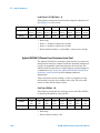
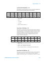
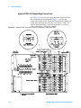
E6198B Integrated Switch/Load Unit Description
The Agilent E6198B now comes as a system integrated unit or
as a standalone unit. The features and functionality remains the
same as the previous E6198A. Differences between the two are
in the cabling and function selection panel.
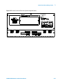
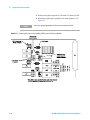
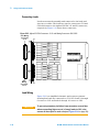
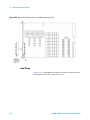
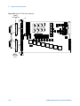
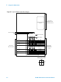
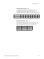
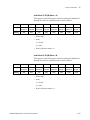
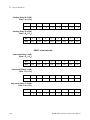
Figure 3-6 E6198B Integrated SLU Back View
Sense Bussed/Split PB Sense Remote/Local Frame Select
E6198B/E6218A Switch/Load Unit User Manual
3-9
J221
94
T8
J102
T9
T1
T5
1
3
T10
94
96
J101
T11
T2
T6
1
3
T12
2
1
2
1
2
1
J1
J3
J2
14
13
14
13
14
13
J803
T13
J801
T3
J104
J105
J111 J110
J106 J107
J802
T7
T14
J109
J108
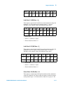
J220 J219 J218 J217 J216 J215 J214 J213 J212 J211 J210 J209 J208 J207 J206 J205 J204 J203 J202 J201
96
T4
BACKPLANE SLU
E6198B/E6218A Switch/Load Unit User Manual
3-10
Switch/Load Unit and Plug-In Cards
3
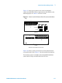
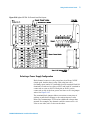
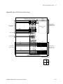
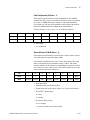
Backplane And Breakout Board Connectors and LEDs
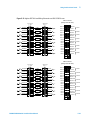
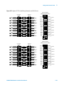
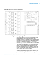
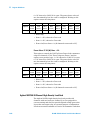
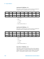
Figure 3-7 Switch/Load Unit Backplane Connectors (USB port adaptor board Not Shown)
3
Switch/Load Unit and Plug-In Cards
Figure 3-7 shows the locations of the various backplane
connectors and LEDs. These components are described on the
following pages. See Table 3-3 for more detail.
Figure 3-8 Switch/Load Unit Breakout Board Connectors (Standalone
only)
J_1
S2A-S2H
S3A-S3F
S1A-S1D
J_8
FRONT
J_5
J_6
J_7
J_3
BACK
BREAKOUT BOARD (External Board)
Figure 3-8 shows connector locations on the breakout board
(external board). Refer Table 3-5 for the detailed descriptions.
The breakout panel is available with the E6198B Standalone
option and is easily accessible from the SLU rear.
E6198B/E6218A Switch/Load Unit User Manual
3-11
3
Switch/Load Unit and Plug-In Cards
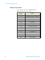
Backplane Connector Name
Table 3-3 lists the connectors on a E6198B backplane.
Table 3-3 Backplane Connectors for E6198B
E6198B Reference
Designator
3-12
Description
J2
SLU Current Sense: Bussed/Split
J3
SLU Power Bus Sense Select: Local/Remote
J1
Frame Select
T1-T14
SLU Logic Power Supply Connector
J101
To USB Controller Connector
J102
Utility Connector
J104
External Reset (reserved)
J105
+5 V Indicator (+5 V Status)
J106
+12 V Indicator (+12 V Status)
J107
–12 V Indicator (–12 V Status)
J108
READY Indicator (Control Status)
J109
+12 V Output For Fan
J110
+12 V Output For Fan
J111
+12 V Output For Fan
J201-J221
Load Card Slots Connector
J801 & J802
Power Busses PB1-PB4
J803
Sense For PB1-PB4
E6198B/E6218A Switch/Load Unit User Manual
3
Switch/Load Unit and Plug-In Cards
Backplane J1, J2 and J3 Connectors
Table 3-4 shows the factory default configuration for the
backplane connectors.
Table 3-4 Backplane Factory Default Connector Settings
Connector
Default
Setting
Description
J1
0 (Zero)
Frame Select address 0-7. When using multiple
Switch/Load Units in your test system, Connector
J1 provides a unique address for each
Switch/Load Unit. Factory default (one
Switch/Load Unit) is 0.
J2
Bussed
Switch/Load Unit Current-Sense Bus
J3
Local
Switch/Load Unit Power Bus Sense select:
Local/Remote
E6198B/E6218A Switch/Load Unit User Manual
3-13
3
Switch/Load Unit and Plug-In Cards
Breakout Board Connector Name (for E6198B Standalone option)
Breakout board extends the connection from backplane to SLU
rear. Table 3-5 lists the description of each connector.
Table 3-5 Breakout Board Connectors
Connector
NOTE
3-14
Description
J_1
Utility Connector (J102 extension connector)
J_3
Utility Connector (J102 internal connector)
J_5
Frame Select & Spare Supply (Connect to J1 of
backplane internal connector)
J_6
Power Bus Sense Local/Remote (Connect to J3 of
backplane internal connector)
J_7
Isense Bussed/Split (Connect to J2 of backplane
internal connector)
J_8
Spare Supply Connector
S1A-S1D
Toggle switches for Local/Remote
S2A-S2H
Toggle switches for Frame Select
S3A-S3F
Toggle switches for Isense Bussed/Split
The breakout board is not available with E6198B System Integrated
option. See Figure 3-6.
E6198B/E6218A Switch/Load Unit User Manual
3
Switch/Load Unit and Plug-In Cards
Backplane Connectors
The following connector descriptions are referenced to
Figure 3-9.
T1-T14 are the Switch/Load Unit power supply connectors.
The supply provides the required +5 V and ±12 V for
powering the backplane and Load Cards. These power supply
lines are protected by fuses.
J102 connects the signals that are cabled between the
Switch/Load Unit and the mass interconnect. These signals
include:
Eight-bit fixture ID pins allow the user to configure a
unique ID for each mass interconnect fixture and read it
back. Address 0 of the backplane is used for the fixture ID
and to read back the status of reset and busy state of the
backplane.
Digital In/Digital Out eight bits each (TTL level).
Open Drain Outputs eight bits each.
Four pairs of current sense busses correspond to the
current sense pairs from slots 1-5, 6-10, 11-15, and 16-21.
These busses may be connected together to form a single bus,
or split into independent current sense busses using jumpers
on SLU backplane J2 connector (Integrated) or switches
S3A-S3F on breakout board (Standalone). Factory default
connects all sense busses to a single bus. Find more
information on when should you split the busses and how in
Chapter 3.
Four remote power bus sense pins remotely sense the
power busses at the UUT. Remote or local sensing for power
bus PB1-PB4 can be set using jumpers on SLU backplane J3
connector or S1A-S1D on breakout board (Standalone).
Factory default is remote sense.
DAC 1 and DAC 2 outputs.
J201-J221 are the slot connectors for Pin Matrix Card or
Load Card, slots 1-21 respectively. The top half of each slot
connector is used to provide slot power, address, data, and
control lines. The bottom half of each connector is used to
connect the power busses to the Load Cards.
E6198B/E6218A Switch/Load Unit User Manual
3-15
3
Switch/Load Unit and Plug-In Cards
J801 and J802 provide the high power connections to power
busses PB1-PB4. Three supplies with a common connection
to PB1 or two independent supplies can be configured on the
four power busses. Bulk bypassing between power busses
may be desirable in certain applications.
J803 provides the sense connections for the four power
busses.
Backplane LEDs
Two sets of LEDs are provided on the backplane for a visual
indication that the Switch/Load Unit is functioning:
Power LEDs. The +5V, +12V and –12V LEDs indicate the status
of the corresponding voltage lines from the Switch/Load Unit
power supply and READY LED indicate the status of SLU ready
to operate. If one or more LEDs is NOT illuminated, the most
likely problem was an overcurrent situation that opened the
non-resettable fuse(s). To change fuse(s), remove power from
the Switch/Load Unit for approximately 20 seconds. The fuse(s)
will reset when power is re-applied. (Non-resettable fuses need
to be replaced rather than power off to reset, refer to Table 3-11
for fuse ratings.)
Frame LEDs. The Frame Access LED flashes to indicate a data
access has occurred to that Switch/Load Unit. The five Slot
Address LEDs indicate the slot currently being addressed.
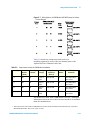
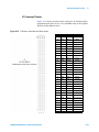
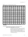
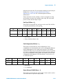
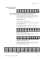
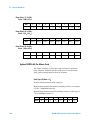
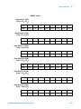
J102 Pinouts
Switch/Load Unit backplane connector J102 carries signals
such as the Digital I/O, DAC 1 and 2, and ISense (current sense)
lines. When configured as part of a standard Agilent system,
J102 of the Switch/Load Unit is connected via cable to a mass
interconnect panel. User connections to the UUT are then made
from the mass interconnect panel. Refer to the appropriate
mass interconnect wiring guide for connection details.
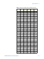
You can also make connections directly to J102 or to the
exposed end of an Agilent E3750-61607, Agilent E6170-61610,
or Agilent E6198-61625 cable connected to J102. Figure 3-9 is a
J102 connector pinout and Figure 3-10 shows the pinouts for
the exposed cable connector end. Table 3-6 defines the signals
available on J102.
3-16
E6198B/E6218A Switch/Load Unit User Manual
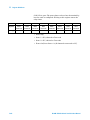
Row 10
Row 9
Row 8
Row 7
Row 6
Row 5
Row 4
Row 3
Row 2
Row 1
Spare_DigOut (3)
Spare_DigOut (1)
Digital In (7)
Digital In (5)
Digital In (3)
Digital In (1)
System Gnd
Fixture ID (7)
Fixture ID (5)
Fixture ID (3)
Fixture ID (1)
System Gnd
Power Bus Sense 2
Row 11
Row 19
Open Drain Out (1)
Power Bus Sense 4
Row 12
Row 20
Open Drain Out (3)
Spare_DigOut (5)
Row 21
Open Drain Out (5)
Row 13
Row 22
Open Drain Out (7)
ISense+ (1)
Row 23
+12 Vdc Supply
Spare_DigOut (7)
Row 24
+12 Vdc Supply
Row 14
Row 25
Spare Supply
Row 15
Row 26
System Gnd
ISense+ (2)
Row 27
System Gnd
Row 16
Row 28
No Connection
ISense+ (3)
Row 29
DAC1
ISense+ (4)
Row 30
DAC2
Row 17
Row 31
Fixture ID (0)
System Gnd
Fixture ID (4)
Fixture ID (2)
Digital In (0)
ISense- (4)
ISense- (1)
Spare_DigOut (2)
Digital In (2)
System Gnd
Fixture ID (6)
Digital In (4)
36 33 30
No Connection
System Gnd
System Gnd
System Gnd
System Gnd
-12 Vdc Supply
+12 Vdc Supply
+12 Vdc Supply
Open Drain Out (6)
Open Drain Out (4)
Open Drain Out (2)
Open Drain Out (0)
Power Bus Sense 3
Power Bus Sense 1
ISense- (3)
ISense- (2)
Spare_DigOut (6)
Spare_DigOut (4)
Spare_DigOut (0)
Digital In (6)
45 42 39
3-17
E6198B/E6218A Switch/Load Unit User Manual
Row 18
Row 32
For E6198B Standalone option, connector J102 is extended from the
backplane to the breakout board. See Figure 3-8.
NOTE
1
C
3
12
6
21 18 15
9
27 24
54 51 48
63 60 57
72 69 66
90 87 84
81 78 75
96 93
4
A
7
10
19 16 13
25 22
34 31 28
43 40 37
52 49 46
61 58 55
70 67 64
79 76 73
88 85 82
94 91
B
NC NC NC NC NC NC NC NC NC NC NC NC NC NC NC NC NC NC NC NC NC NC NC NC NC NC NC NC NC NC NC NC
3
Switch/Load Unit and Plug-In Cards
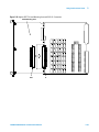
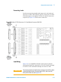
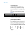
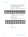
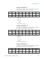
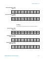
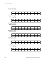
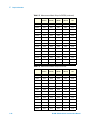
Figure 3-9 Switch/Load Unit J102 Connector Pinouts
3
Switch/Load Unit and Plug-In Cards
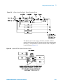
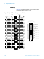
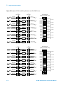
Figure 3-10 Cable Connector Pinouts
Cable Connector Endand Front View
(Center Column Not Used)
System Gnd
Row 1
Fixture ID (0)
Row 2
Fixture ID (2)
Row 3
Fixture ID (4)
Row 4
Fixture ID (6)
Row 5
System Gnd
Row 6
Digital In (0)
Row 7
Digital In (2)
Row 8
Digital In (4)
Row 9
Digital In (6)
Row 10
Spare_DigOut (0)
Row 11
Spare_DigOut (2)
Row 12
Spare_DigOut (4)
Row 13
Spare_DigOut (6)
Row 14
ISense- (1)
Row 15
ISense- (2)
Row 16
ISense- (3)
Row 17
ISense- (4)
Row 18
Row 19 Power Bus Sense 1
Row 20 Power Bus Sense 3
Row 21 Open Drain Out (0)
Row 22 Open Drain Out (2)
Row 23 Open Drain Out (4)
Row 24 Open Drain Out (6)
Row 25
+12 Vdc Supply
Row 26
+12 Vdc Supply
Row 27
-12 Vdc Supply
System Gnd
Row 28
System Gnd
Row 29
Row 30
No Connection
Row 31
System Gnd
Row 32
System Gnd
3-18
A B C
1 System Gnd
3
6
4 Fixture ID (1)
9
7 Fixture ID (3)
12
10 Fixture ID (5)
15
13 Fixture ID (7)
18
16 System Gnd
21
19 Digital In (1)
24
22 Digital In (3)
27
25 Digital In (5)
30
28 Digital In (7)
33
31 Spare_DigOut (1)
36
34 Spare_DigOut (3)
39
37 Spare_DigOut (5)
42
40 Spare_DigOut (7)
45
43 ISense+ (1)
48
46 ISense+ (2)
51
49 ISense+ (3)
53
52 ISense+ (4)
57
55 Power Bus Sense 2
60
58 Power Bus Sense 4
63
61 Open Drain Out (1)
66
64 Open Drain Out (3)
69
67 Open Drain Out (5)
72
70 Open Drain Out (7)
75
73 +12 Vdc Supply
78
76 +12 Vdc Supply
81
79 Spare Supply
84
82 System Gnd
87
85 System Gnd
90
88 No Connection
93
91 DAC1
96
94 DAC2
E6198B/E6218A Switch/Load Unit User Manual
3
Switch/Load Unit and Plug-In Cards
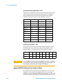
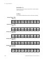
Table 3-6 J102 signal definitions
+12Vdc, –12Vdc
Supply
+12V and –12V from the Switch/Load Unit Power Supply. The +12V supply can deliver
12.5A, the –12V supply can deliver 2.1A.
Spare Supply
Connection for a user installed power supply not included in the standard system. Refer
to “Connecting an Additional (Spare) Power Supply" for details.
DAC1
DAC2
The Switch/Load Unit provides two 14-bit channels of DAC which supply ±16 V at 10 mA
each.
Digital In 0 - 7
Open Drain Out 0 - 7
Spare_DigOut
The Switch/Load Unit provides 8-bits of digital input, 8-bits of open drain digital output,
and 8-bits of TTL-level digital output (Spare_DigOut). There is no handshaking
capability.
Fixture ID (0 - 7)
The Fixture ID lets you configure a unique ID for each mass interconnect fixture and
read it back. ID sent as TTL level bits.
Isense+ (1 - 4)
Isense– (1 - 4)
These lines connect to the current sense bus on the Switch/Load Unit backplane. These
lines are used for sensing current on a selected load card channel. The 8-channel and
16-channel load cards are designed to connect to the current sense bus. Each load card
channel’s current sense lines are multiplexed so that on each card only one channel at a
time can be connected to the current sense bus. The current sense lines and the slots
they connect to are:
Isense lines (1) connect to Switch/Load Unit slots 1 - 5.
Isense lines (2) connect to Switch/Load Unit slots 6 - 10.
Isense lines (3) connect to Switch/Load Unit slots 11 - 15.
Isense lines (4) connect to Switch/Load Unit slots 16 - 21.
Two or more sets of the above lines can be bussed together select from toggle switches.
Refer to page 12 for details.
Power Bus Sense 1 - 4
The remote sense lines for the power supplies connected to power buses 1 - 4.
Gnd
Chassis ground of the Switch/Load Unit.
E6198B/E6218A Switch/Load Unit User Manual
3-19
3
Switch/Load Unit and Plug-In Cards
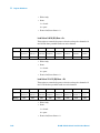
J1 Pinout
Table 3-7 shows pinout of J1 Frame Select & Spare Supply (SS).
Frame 0 is selected if FS0 and FRAME are both are connected;
Frame 1 is selected if FS1 and FRAME are both are connected,
and so on. Default setting is frame 0 (zero). More detail about SS
(Spare Supply), please refer “Connecting an Additional (Spare)
Power Supply" .
Table 3-7 Switch/Load Unit J1 Pinout
FS1
FS3
FS5
FS7
NC
GND
SS
FS0
FS2
FS4
FS6
FRAME
GND
SS
J2 Pinout
Table 3-8 show pinouts of J2 ISENSE Bussed/Split. Default
setting for J2 is ISENSE Bussed.
Table 3-8 Switch/Load Unit J2 Pinout
IS(-2)
IS(+2)
IS(-3)
IS(+3)
IS(-4)
IS(+4)
NC
IS(-1)
IS(+1)
IS(-2)
IS(+2)
IS(-3)
IS(+3)
NC
J3 Pinout
Table 3-9 shows pinouts of Power Bus Sense Local/Remote.
Local 1 is selected if LOC_S1 is connected with PB1; Remote 1 is
selected if REM_S1 is connected with PB1, and so on. Default
setting for J3 is Local.
Table 3-9 Switch/Load Unit J3 Pinout
3-20
LOC_S1
PB2
REM_S2
LOC_S3
PB4
REM_S4
LOC_S1
PB1
REM_S1
LOC_S2
PB3
REM_S3
LOC_S4
PB1
E6198B/E6218A Switch/Load Unit User Manual
Switch/Load Unit and Plug-In Cards
3
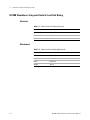
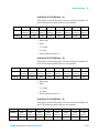
T1-T14 SLU Logic Power Supply Connector
T1-T14 provides the required +5 V and ±12 V for powering the
backplane and Load Cards. Table 3-10 lists each jumper and its
corresponding input voltage.
Table 3-10 Power Supply Input for each Jumpers
Jumper
E6198B/E6218A Switch/Load Unit User Manual
Input Voltage
T1
+5 V
T2
+5 V
T3
+5 V
T4
–12 V
T5
+12 V
T6
+12 V
T7
+12 V
T8
GND
T9
GND
T10
GND
T11
GND
T12
GND
T13
GND
T14
GND
3-21
3
Switch/Load Unit and Plug-In Cards
Differentiating E6198B Standalone Option and System Integrated Option
The key differences between the standalone and system
integrated option can be found at the SLU rear cover.
On a standalone unit, the backplane connectors are extended to
the breakout board attached to the SLU rear cover. At the SLU
rear, you will find toggle switches for SLU configuration, and
power and sense buses connectors protected by a cable
enclosure. (See Figure 3-11.)
On a system integrated unit, you will find cut-outs on the SLU
rear cover to allow cable routing from the SLU backplane.
Jumpers are used for SLU configuration.
Figure 3-11 Switch/Load Unit Rear View (Standalone Option)
3-22
E6198B/E6218A Switch/Load Unit User Manual
Switch/Load Unit and Plug-In Cards
3
Figure 3-12 Switch/Load Unit Rear View (System Integrated Option)
E6198B/E6218A Switch/Load Unit User Manual
3-23
3
Switch/Load Unit and Plug-In Cards
Fuse Ratings
Fuses are incorporated inside E6198B Switch/Load Unit. There
are 10 fuses and 7 fuses for Standalone SLU and Integrated SLU
respectively. Please refer Table 3-11 for more detail.
Table 3-11 Fuses Ratings
Standalone
Integrated
Description
Fuse1
Fuse1
1 A, –12 V
Fuse2
Fuse2
6 A, +12 V_1
Fuse3
Fuse3
6 A, +12 V_2
Fuse4
Fuse4
Not Used
Fuse5
Fuse5
15 A, +5 V_1
Fuse6
Fuse6
15 A, +5 V_2
Fuse7
Fuse7
Not Used
Fuse8
-
30 A, PB2
Fuse9
-
30 A, PB3
Fuse10
-
30 A, PB4
DC Power Bus Connections
PB1 to PB4 are the DC power bus connections as seen in
Figure 3-11 for the standalone unit. Notice the protective cable
enclosure covering both the power bus cabling and power sense
cabling for better protection.
For the integrated unit, there is no protective cable enclosure,
and you will need to configure the cabling directly onto the
backplane, behind the SLU backcover.
3-24
E6198B/E6218A Switch/Load Unit User Manual
Agilent TS-5000
E6198B Switch/Load Unit User Manual
4
Configuring the Switch/Load Unit
Card Location Recommendations 4-2
Connecting an Additional (Spare) Power Supply 4-5
Configuring the Power Busses 4-6
Connecting E6198B to the Computer via USB Interface or Parallel
Port 4-12
Adding a Second Switch/Load Unit 4-13
Load Box Installation 4-14
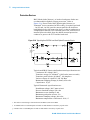
This chapter shows you how to configure the Switch/Load Unit.
WA RNING
SHOCK HAZARD. Only service-trained personnel who are aware
of the hazards involved should install, remove, or configure the
Switch/Load Unit or plug-in cards. Before you remove any
installed card, disconnect AC power from the mainframe and from
other cards that may be connected to the cards.
CAUTION
STATIC ELECTRICITY
Static electricity is a major cause of component failure. To prevent
damage to electrical components, observe anti-static techniques
whenever installing or removing a card in the Switch/Load Unit or
whenever working on a card.
Agilent Technologies
4-1
4
Configuring the Switch/Load Unit
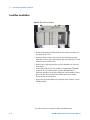
Card Location Recommendations
Slot 1 to 21 of a Switch/Load Unit are identical and able to take
any supported Pin Matrix or Load Cards. This sections provides
an example on card installation guideline to maintain
consistency between test systems. Your test system may use a
different guideline that fits your application.
For a single Agilent E6198B Switch/Load Unit installed in the
system
Install matrix cards first. Slots 15 through 21 are reserved for
the matrix and custom modules. Starting from slot 21 and
working down, install matrix modules and custom modules in
the following order:
• Agilent Pin Matrix and Instrument Multiplexer Card
(E8792A or E8782A)
• Agilent Pin Matrix Card(s) (E8793A and/or E8783A)
• Agilent E8794A Custom Card(s)
Install the load cards using the following rules:
• Agilent N9379A 48-Channel Load Cards
Install any N9379A cards first, starting at slot #1.
• Agilent E6177A 24-Channel Load Cards
Install any E6177A cards next.
• Agilent U7177A 24-Channel Load Cards with Current
Sense
Install any U7177A cards next.
• Agilent N9378A 24-Channel Load Cards
Install any N9378A cards next. To allow for future expansion,
leave an open slot after the last N9378A card.
• Agilent E6176A 16-Channel Load Cards
Install any Agilent E6176A cards next.
• Agilent N9377A 16-Channel Load Cards
Install any Agilent N9377A cards next. To allow for future
expansion, leave an open slot after the last N9377A card.
• Agilent E6178B 8-Channel Heavy Duty Load Cards
Agilent E6178B 8 channel Heavy Duty cards require two slots
each. These cards are installed in even slot locations only.
Install E6178B cards starting with the first available even
slot following the 16 channel cards.
4-2
E6198B/E6218A Switch/Load Unit User Manual
4
Configuring the Switch/Load Unit
• Agilent E6175A 8-Channel Load Cards
Agilent E6175A 8 channel cards require two slots each.
These cards are installed in even slot locations only. Install
E6175A cards in first available even slot following the
E6178B 8-Channel Heavy Duty cards.
Please close the gap for rear side of the connector if using own
fabricated cable with connector.
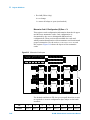
CAUTION
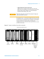
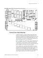
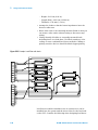
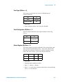
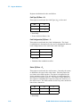
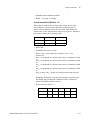
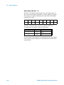
For example, Figure 4-1 shows the standard locations for matrix
and load cards for a system which contains three matrix cards,
a custom card, two 24 channel, four 16 channel, one 8 channel,
and one 8 channel heavy duty load card. If using this
configuration, be sure to leave the slots open between the cards,
as shown in the figure.
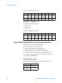
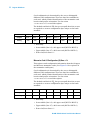
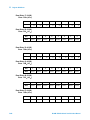
Figure 4-1 Example of Load/Matrix/Custom Cards Loading Order
Switch/Load Unit Slot Front View
N9379A
48-Channel
6
7
8
E6177A
24-Channel
9
N9378A
24-Channel
E6198B/E6218A Switch/Load Unit User Manual
10 11 12 13 14 15 16 17 18 19 20 21
Agilent E6176A N9378A
16-Channel
24-Channel
Load Cards
Empty
5
Empty
4
Empty
3
Empty
2
Empty
1
Empty
Slot:
E6175A
8-Channel
Agilent E8794A
Custom Card
E8792A 32-Pin
Matrix and
Instrument
Multiplexer
Card
4-3
4
Configuring the Switch/Load Unit
Load Card Types and IDS
Each card is assigned a different type and has a 10-pin
connector that lets you assign a unique binary code ID number
to each card. See“Load Card Type and Configuration ID" for
more information.
4-4
E6198B/E6218A Switch/Load Unit User Manual
Configuring the Switch/Load Unit
4
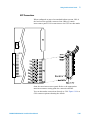
Connecting an Additional (Spare) Power Supply
The Spare Supply pinout located at SLU backplane connector J1
(Integrated) allows you to add an additional power supply such
as a +24 V power supply for powering higher voltage relays. It is
necessary to remove the SLU rear cover to access this
connector. Figure 4-2 shows the placement and orientation on
the backplane for the power supply components. Both
Connector J1 and Capacitor C507 are loaded at the factory.
Capacitor C507 is to minimize high-frequency noise on the
supply line. The auxiliary supply output (Spare Supply) appears
on Switch/Load Unit connector J102 pin 79.
Figure 4-2 Component Location/Schematic for User-Installed External Power Supply
RT505
700m
HP 0837-0440
J1
2
14
1
13
V+24V
To J102
J1
SS ( +ve Polarity)
Raytheon P/N
SMD100 or
equivalent
C507
100uF
50V
HP 0180-3334
+
For SLU Standalone option, you can connect to the Spare
Supply Input directly from SLU rear. See Figure 4-3.
Figure 4-3 Spare Supply (Input) Connector on SLU rear (SLU standalone)
E6198B/E6218A Switch/Load Unit User Manual
4-5
4
Configuring the Switch/Load Unit
Configuring the Power Busses
The UUT power supplies are connected to the power busses
PB1-PB4. Figure 4-4 shows the power bus connectors J801 and
J802 located on the Switch/Load Unit backplane for integrated
option. These connectors use screw terminations for high
current. The J801 connectors are shorted on board, providing a
common connection for up to three supplies. Example A and B
below show the two most common ways of configuring the
power busses.
Figure 4-4 Power Bus Connectors J801 and J802
PC Board Traces
PB1
J801
PB2
PB3
PB4
J802
The following examples A and B show the two most common
ways of configuring the power busses.
Example A shows three separate supplies attached to the
busses, with all three sharing a common ground on Power Bus 1
(PB1). This is the factory default configuration. The grounds for
all three supplies are connected together on connector J801.
4-6
E6198B/E6218A Switch/Load Unit User Manual
Configuring the Switch/Load Unit
4
Figure 4-5 Example A: Three Separate Supplies on PB1 - PB4
PB1
PB2
PB3
PB4
+12V
-12V
+5V
Example B (available only as a special configuration) shows two
isolated power supplies with separate grounds connected to the
power bus. This configuration can be used if, for example, one
supply requires local sensing, while the other requires remote
sensing at the UUT.
Figure 4-6 Example B: Isolated Power Supplies
PB1
PB2
VBATT
PB3
VUUT
PB4
For the standalone SLU, users can directly connect to the
external connector “DC Power Bus Connection”. (See
Figure 4-7.)
E6198B/E6218A Switch/Load Unit User Manual
4-7
4
Configuring the Switch/Load Unit
Figure 4-7 DC Power Bus Connector Of Standalone SLU
Power Bus 1
Power Bus 2
Power Bus 3
Power Bus 4
PB Sense 1
PB Sense 3
PB Sense 2
PB Sense 4
Setting the UUT Power Supply Remote/Local Sense Jumpers
The UUT power supplies can be configured for either remote
sense or local sense. In local sense, the voltage across the load
equals the power supply voltage less the voltage drop across the
cables between the load and power supply. In remote sense, the
voltage across the load equals the selected power supply
voltage. In this configuration, the power supply automatically
increases the voltage output to compensate for the voltage drop
across the cables. A conceptional view of both types of sensing
is shown in Figure 4-8.
4-8
E6198B/E6218A Switch/Load Unit User Manual
4
Configuring the Switch/Load Unit
Figure 4-8 Conceptional View of Local/Remote Sensing
Set the power supply sense jumpers in the LOCAL position for
sensing the power supply outputs at the PB1 - PB4 terminals.
For Standalone, toggle PB Sense Remote/Local switches to
select either Remote or Local mode. See Figure 4-9.
E6198B/E6218A Switch/Load Unit User Manual
4-9
4
Configuring the Switch/Load Unit
Figure 4-9 PB Sense Remote/Local Interface (Standalone SLU)
For Integrated, use Jumper to select the mode on PB Sense
Remote/Local. See Figure 4-10.
Figure 4-10 PB Sense Remote/Local and Frame Select Interface
(Integrated SLU)
Configuring the Current-Sense Jumpers
The Switch/Load Unit is shipped from the factory with the
current-sense jumpers J2 installed in the BUSSED position
forming one continuous current-sense bus along the
Switch/Load Unit backplane. These three jumpers have been
included so that, if necessary, the existing single current-sense
bus can be split up into as many as four independent
current-sense busses by changing the jumper location to SPLIT.
Each independent current-sense bus provides one reading, so
up to four simultaneous current-sense readings can be made at
a time.
The hardware allows each card to perform current-sense
measurements on only one channel at a time. However, it is
possible to command two cards sharing a common
current-sense bus to attempt simultaneous current-sense
readings. This can lead to a power bus to power bus short,
causing confused and incorrect readings.
4-10
E6198B/E6218A Switch/Load Unit User Manual
4
Configuring the Switch/Load Unit
Figure 4-11 shows the ISense Bussed/Split interface for
Standalone SLU. Toggle the switch to choose either Bussed or
Split mode.
Figure 4-11 ISense Bussed/Split Interface (Standalone SLU)
For system integrated SLU, jumpers are used to select between
Bussed/Split, see Figure 4-12.
Figure 4-12 ISense Bussed/Split Interface (Integrated SLU)
NOTE
Ensure Load Cards that will be accessed simultaneously for current-sense
readings are located in slots that do not share a common current-sense
bus.
E6198B/E6218A Switch/Load Unit User Manual
4-11
4
Configuring the Switch/Load Unit
Connecting E6198B to the Computer via USB Interface or Parallel Port
USB interface is introduced in E6198B, on top of parallel port
interface which is available on the older version on SLU. The
USB interface connects to the PC controller using a standard
USB cable. See Figure 4-13.
Figure 4-13 USB Cable Connections
4-12
E6198B/E6218A Switch/Load Unit User Manual
4
Configuring the Switch/Load Unit
Adding a Second Switch/Load Unit
You can add a second Switch/Load Unit to the system as the
load and switching requirements increase. Connection to the PC
controller can be made to any existing USB port or via an
externally powered USB hub.
For Standalone SLU, the Frame Select toggle switches, sets the
address of each Switch/Load Unit (see Figure 4-14). The toggle
switches can be set for any address from zero to seven.
However, for the Integrated SLU, jumpers must be used for
frame select. For each system, no two Switch/Load Units can
have the same address. The factory default position is Address
0. As an example, you can leave the address of the first
Switch/Load Unit set to 0 and set the address of the second
Switch/Load Unit to 1.
Figure 4-14 Frame Select Interface (Standalone SLU)
E6198B/E6218A Switch/Load Unit User Manual
4-13
4
Configuring the Switch/Load Unit
Load Box Installation
Figure 4-15 Load Box Installed
• Install 4 tinnermans (0590-0804) at the proper locations on
the back of the rack.
• From the back of the rack, position the load box onto the
rails and secure to the rack using 4 spacers (0380-0317*) and
4 dress screws (0570-1272).
• Spacers are only required for the first loadbox (to clear the
door latch).
• Check the build list for the number of load boxes (E6198B)
required. If a second load box (Option E6198B-FG) is
required, another set of rails will need to be installed. Allow
space for the first load box and 1 EIA space for venting
between the two load boxes.
• Secure the second loadbox (if required) with 4 dress screws
(E9900-06001).
* This is the standard spacer. For E8972 (TS-5400), use 0380-4697 spacers.
4-14
E6198B/E6218A Switch/Load Unit User Manual
Agilent TS-5000
E6198B Switch/Load Unit User Manual
5
Using Load Cards and Loads
Load Card Capabilities 5-2
Loads Overview 5-4
Using the Load Cards 5-5
Using the Agilent E6175A 8-Channel Load Card 5-7
Using the Agilent E6176A 16-Channel Load Card 5-25
Using the Agilent E6177A 24-Channel Load Card 5-38
Using the Agilent U7177A 24-Channel Load Card 5-47
Using the Agilent E6178B 8-Channel Load Card 5-55
Using the Agilent U7178A 8-Channel Heavy Duty Load Card 5-63
Using the Agilent U7179A 16-Channel High Current Load Card 5-71
Using the Agilent N9377A 16-Channel Dual-Load Load Card 5-83
Using the Agilent N9378A 24-Channel Low Resistance Load Card 5-97
Using the Agilent N9379A 48-Channel High-Density Load Card 5-105
This chapter discusses how to configure load cards and how to
use loads with the various load cards.
Agilent Technologies
5-1
5
Using Load Cards and Loads
Load Card Capabilities
Table 5-1 Load Card Capabilities
Function
Slot Size
No. of
Channels
(Max.)
No. of
Channels Unshared
Relays
Maximum
Current per
Channel
Current
Measuring
with Sense
Resistor
Current
Measuring
with Current
Transducer
Flyback
Protection
Available
(User
Installed)
E6175A
2
8
4
7.5 A
(15 A peak)
Yes
Yes
Yes
E6176A
1
16
16
7.5 A
(15 A peak)
Yes
No
Yes
E6177A
1
24
24
2A
No
No
No
E6178B
2
8
8
30 A
No
Yes
Yes
N9377A
1
16 dual load
16
7.5 A
(15 A peak)
Yes
No
Yes
N9378A
1
24 dual load
24
2A
No
No
No
N9379A
1
48 dual load
48
2A
No
No
No
U7177A
1
24
24
2A
Yes
No
No
U7178A
2
8
8
40 A
No
Yes
Yes
U7179A
2
16
16
15 A
Yes
No
Yes
• The Agilent E6175A 8-Channel High Current Load Card, with
integral current sensing, is intended to be used with loads
mounted on the card. A 9-inch by 4-inch area of sheet metal
is open on the front of the card for mounting loads. The card
is two slots wide to allow mounting of larger loads.
• The Agilent E6176A 16-Channel High Current Load Card is a
single-slot design, requiring externally mounted loads. This
load card offers high load density for high current loads
where current transducers and bridge drive configuration
are not required.
• The Agilent E6177A 24-Channel Medium Current Load Card
(for non-inductive loads) is intended to be used with loads
mounted on the card. A 9-inch by 4-inch area of sheet metal
is open on the front of the card for mounting small loads.
This card is one slot wide and capable of up to 2A continuous
carry current.
5-2
E6198B/E6218A Switch/Load Unit User Manual
Using Load Cards and Loads
5
• The Agilent U7177A 24-Channel Medium Current Load Card
(for non-inductive loads), with integral current sensing, is
intended to be used with externally mounted loads. This card
is one slot wide and capable of up to 2A continuous carry
current.
• The Agilent E6178B 8-Channel Heavy Duty Load Card is
designed for very high current applications of up to 30A per
channel.
• The N937xA load cards support multiple loads per channel,
either dual loads (two loads per channel) or quad loads (four
loads per channel).
• The Agilent U7178A 8-Channel Heavy Duty Load Card is
designed for very high current applications of up to 40 A per
channel.
• The Agilent U7179A 16-Channel High Current Load Card is
designed for high current applications, requiring externally
mounted loads. This card is capable of up to 15 A continuous
carry current.
E6198B/E6218A Switch/Load Unit User Manual
5-3
5
Using Load Cards and Loads
Loads Overview
Figure 5-1 shows a conceptual block diagram of a typical load
application having these four main areas:
• Power Supply
• Load Card
• Loads
• Unit Under Test (UUT)
Figure 5-1 Loads/Sources Conceptual Overview
Simplified Load Card
NO
Unit Under Test
V+
Power Bus 2
Power Bus 1
+
Power
Supply
Nc
NO
Nc
GND
NO
Nc
External Loads and Shorts
5-4
E6198B/E6218A Switch/Load Unit User Manual
5
Using Load Cards and Loads
Using the Load Cards
This section describes how to configure and use the load cards.
Load Card Type and Configuration ID
Each load card type is assigned a card type number as follows:
Agilent E6175A 8-Channel: Card Type is 1
Agilent E6176A 16-Channel: Card Type is 2
Agilent E6177A 24-Channel: Card Type is 3
Agilent U7177A 24-Channel: Card Type is 24
Agilent E6178B 8-Channel Heavy Duty: Card Type is 4
Agilent N9378A 24-Channel Low Resistance: Card Type is 5
Agilent N9379A 48-Channel High Density: Card Type is 6
Agilent N9377A 16-Channel Dual Load: Card Type is 7
Agilent U7178A 8-Channel Heavy Duty: Card Type is 25
Agilent U7179A 16-Channel High Current: Card Type is 32
Except for the N9378A and N9379A, each load card is equipped
with a 10-pin connector to allow assignment of a unique binary
code ID number to each card. This is useful for verifying a
particular configuration of the cards in the SLU. Refer to
Figure 5-2.
Figure 5-2 Pin Assignments on the Card Configuration Jack
• Pin 1 is used for bit 8 on the N9377A card only
• Pins 2-5 correspond to bits 0-3, respectively
• Pins 7-10 correspond to bits 4-7, respectively
E6198B/E6218A Switch/Load Unit User Manual
5-5
5
Using Load Cards and Loads
• See “Connecting Loads" for more information on addressing
loads on the N9378A load card.
• See “Connecting Loads" for more information on addressing
loads on the N9379A load card.
The configuration pins are normally high with a 10 KΩ pull-up
resistor resident on the load card, producing a value of FFh.
Grounding selected pins creates binary codes which can be read
back through the interface using the loadCardGetInfo action. See
the TS-5000 System Software User’s Guide for more
information.
5-6
E6198B/E6218A Switch/Load Unit User Manual
5
Using Load Cards and Loads
Using the Agilent E6175A 8-Channel Load Card
The Agilent E6175A 8-channel high-current load card, with
current sensing, is intended to be used with loads mounted
inside the Switch/Load Unit. This card provides great flexibility,
low series resistance, and high current-carrying capability.
Figure 5-3 shows a block diagram of the Agilent E6175A
8-Channel Load Card. The card layout is shown in Figure 5-4.
• The card is two slots wide (4 cm./1.6 inches) to allow
mounting of larger loads. Due to its high current capability, it
is recommended that you mount it on the left side (slots 1-4)
of the Agilent E6198B Switch/Load Unit enclosure, closest to
the incoming power buses. “Card Location
Recommendations"
• The card type is 01h. “Load Card Type and Configuration ID".
• The factory default is to load a 0.05Ω, 0.1% Isense resistor in
each channel. If you prefer to use a current transducer, you
must remove the Isense resistor and add the current
transducer described in “Selecting a Current-Sense Method".
• A nine-inch by four-inch area of sheet metal is left open on
the front of the card for mounting loads. You provide the load
mounting hardware, drilling holes in the sheet metal as
needed. “Connecting Loads".
• Each channel is capable of up to 7.5 amperes continuous
carry current or up to 15 amperes with a two percent duty
cycle.
• There is a slow blow fuse on each channel to protect the card
traces against extended high current operation.
E6198B/E6218A Switch/Load Unit User Manual
5-7
5
Using Load Cards and Loads
Figure 5-3 Agilent E6175A 8-Channel High-Current Load Card Block Diagram
5-8
E6198B/E6218A Switch/Load Unit User Manual
Using Load Cards and Loads
5
Figure 5-4 Agilent E6175A 8-Channel Load Card Layout
Selecting a Power Supply Configuration
Each channel pair connects to the power bus via a Form C SPDT
(single-pole, double-throw) relay. This relay has an NO
(normally-open) and an NC (normally-closed) terminal. Each
NO terminal is connected to a pin on J3, and each NC terminal
is connected to a pin on J4. Each pin on J3 or J4 can be
connected to any of the four power bus lines on J5 via jumper
wires. This arrangement allows convenient pull-up or pull-down
of the various inputs. It also allows for terminating a UUT load
at a different voltage than ground.
E6198B/E6218A Switch/Load Unit User Manual
5-9
5
Using Load Cards and Loads
The factory default is to provide two jumper combs, one that
ties all the pins on J3 together and one that ties all the pins on
J4 together. The NO pins are jumpered to power bus 2, and the
NC pins are jumpered to power bus 1. The jumper combs for J3
and J4 can be easily cut to provide bus or pin isolation between
the various input/power bus connections. For example, if you
use one of the channel pairs in a bridge configuration, you
would probably disconnect that channel from the J4 jumper
comb to eliminate possible power bus interaction.
Selecting a Current-Sense Method
There are two ways to measure current on the Agilent E6175A
8-Channel Load Card; using a sense resistor, or using a LA
25-NP current transducer from LEM Inc.* Figure 5-5 shows the
relationship between the sense resistor (Rs) and the LEM
module current transducer (only one or the other is used, never
both).
Sense Resistors
The card comes factory loaded with a 3-watt, 0.05 Ω, 0.1% sense
resistor already installed. This is the lowest value sense resistor
that can safely be installed. If lower value currents are being
measured, requiring a larger resistance value to make the sense
voltage readable, then this sense resistor can be replaced by a
four-wire resistor of higher value. The sense resistor should
suffice for most measurements except those that require that
the measurement be isolated from high common-mode voltage
transients.
Current Transducers
The load card is designed to accept a LEM current transducer
(LEM module) to be inserted in the circuit in place of the
current-sense resistor.
* This module was tested with a LEM Model LA25-NP Current Transducer from LEM USA, Inc. 6643 West
Mill Road, Milwaukee, WI, 53218. (414) 353-0711
5-10
E6198B/E6218A Switch/Load Unit User Manual
5
Using Load Cards and Loads
Figure 5-5 LEM Current Transducer
Installing a LEM Current Transducer
Figure 5-6 shows the component location of the current-sense
section of the first two channels on the load card. The location
of the components listed in Table 5-2 are silk-screened on the
load card's printed circuit board. Installing a current transducer
involves both elements of a channel pair. For example, if the
LEM module were to be installed across channels 1-2:
1 Remove the 0.05Ω current-sense resistor (R1).
CAUTION
The current-sense resistor must be removed from the
Agilent E6175A PC board.
2 Install the LEM module.
3 Install the measuring resistor, R2 (preferably a 100Ω, 0.1%
resistor).
4 Install the shorting jumper from R2 to ground, TP41 to
TP42.
E6198B/E6218A Switch/Load Unit User Manual
5-11
5
Using Load Cards and Loads
5 Install two bypass capacitors, C41 and C42, both 0.01 μF.
6 Install the appropriate primary-coil range jumpers. See
Figure 5-7.
NOTE
Use a wire gauge appropriate for the current through the load.
Figure 5-6 Component Location for Installing LEM Current Transducer Module
5-12
E6198B/E6218A Switch/Load Unit User Manual
5
Using Load Cards and Loads
Figure 5-7 Wiring Options of LEM Model LA25-NP Primary for Various
Current Ranges
Table 5-2 details the components that need to be
installed/replaced for each of the two channel pairs of the
Agilent E6175A 8-Channel Load Card.
Table 5-2
Components involved in LEM Module Installation
Channel(s)
Isense
Resistor
(Rmvd)
Measuring
Resistor
Shorting
Jumper
Bypass
Capacitors
(0.01 μf)
LEM
Module
LEM Tap
Connection
1, 2
R1
R2
TP41 to
TP42
C41 and C42
U1
See LEM module
Spec. Sheet
3, 4
R3
R4
TP43 to
TP44
C43 and C44
U2
See LEM module
Spec. Sheet
5, 6
R5
R6
TP45 to
TP46
C45 and C46
U3
See LEM module
Spec. Sheet
7, 8
R7
R8
TP47 to
TP48
C47 and C48
U4
See LEM module
Spec. Sheet
The board was tested with a LEM Model LA25-NP*. Additional
information about the use of this current transducer is available
from the manufacturer.
* This load card was tested with a LEM Model LA25-NP Current Transducer from LEM USA, Inc. 6643 West
Mill Road, Milwaukee, WI, 53218. (414) 353-0711
E6198B/E6218A Switch/Load Unit User Manual
5-13
5
Using Load Cards and Loads
Selecting and Loading Flyback Protection
Coils used as loads may have large flyback voltages which have
the potential to damage other electronic components. Generally,
the UUTs are equipped with flyback protection, so flyback
protection on the load cards is redundant but provides
additional back-up protection in case a defective UUT is tested.
The system integrator is responsible for ensuring flyback
protection devices are installed on the load cards.
CAUTION
The load cards are designed to handle a maximum of 500
Vpeak flyback voltage. Operating the load cards without
flyback protection installed on the appropriate channels, or
with flyback voltages in excess of 500 Vpeak, may results in
damage to the load card or SLU.
The Agilent E6175A 8-Channel Load Card comes with
provisions for user-installed flyback voltage protection.
Figure 5-9 is a detail of the first channel pair, channels 1 and 2,
on the component locator diagram of the 8-Channel Load Card.
It shows the location and polarity orientation for channel 1's
(RT1 and RT2) and channel 2's (RT3 and RT4) flyback
protection devices. This pattern is repeated for the other three
channel pairs.
As an example, in Figure 5-8 Chan1 has two potential input
lines connected to the input Form C switch K11. RT1 connects
input line J4 and RT2 connects alternate input line J3, to the
output of Load1. When a voltage spike occurs on the UUT that
exceeds the rating on the flyback device, the device clamps the
surge voltage to the device’s predetermined value.
5-14
E6198B/E6218A Switch/Load Unit User Manual
Using Load Cards and Loads
5
Figure 5-8 8-Channel Load Card Detail - Flyback Protection Circuit
The flyback protection devices should be installed with the
positive side towards the UUT. On each of the four channel pairs
the high (+) side should be located as shown in the component
locator diagram, Figure 5-9.
Figure 5-9 Agilent E6175A Flyback Protection Polarity
E6198B/E6218A Switch/Load Unit User Manual
5-15
5
Using Load Cards and Loads
Protection Devices
MOV (Metal Oxide Varistor), or back-to-back zener diodes are
recommended for flyback voltage protection.* Refer to
Figure 5-10. Zener Diode, MOV (Metal-Oxide Varistor) or
Transzorb® devices mounted at RTx or RTy (2 required per load
- 1 at NC and 1 at NO) provide current path for the inductive
load flyback. Select the protection device so that it conducts at a
voltage higher than the UUT's internal protection. If the device's
internal protection fails, then the added external protection
conducts to protect the UUT and the load card.
Figure 5-10 Typical Agilent E6175A Load Card Flyback Protection Circuit
+
16V
-
Typical small MOV (3mm) axial lead mounted specifications are:
Continuous DC voltage: 220 V
Transient energy (10/1000mS)†: 0.90 Joules (watt-seconds)
Transient peak current (8/20mS)‡: 100 Amperes
Varistor voltage @ 1.0mA DC: 300 Vdc Max
Maximum Clamping Voltage (8/20mS): 450 volts
Capacitance: 17 pF
Typical Transzorb® specifications are:
Breakdown voltage: 300 V max at 1mA
Reverse Standoff voltage: 250 volts
Maximum reverse leakage: 5 mA
Maximum peak pulse current: 5 A
Maximum Clamping voltage: 400 volts
Maximum temperature coefficient: 0.110%/°C
* The card was tested using a General Electric GE MOV II, MA series MOV.
† 10/1000mS refers to a standard pulse of 10mS rise and 1000mS to 50% decay of peak value.
‡ 8/20mS refers to a standard pulse of 8mS rise and 20mS to 50% decay of peak value.
5-16
E6198B/E6218A Switch/Load Unit User Manual
5
Using Load Cards and Loads
Selecting a Load Fuse
The load fuses used are IEC 5x20 mm, 5-ampere slow-blow.
These fuses may be replaced by larger fuses if required by your
equipment, but not to exceed 8 amperes. In any event, the
maximum fuse rating must not exceed an I2T value of 102-126.*
Sample Load Configurations
Four sets of tandem loads, each set sharing a current-sense
resistor, may be mounted on the Agilent E6175A Load Card. You
may need to drill holes in the sheet metal to attach the loads. On
the eight-channel load card, the pairs are labeled 1 through 4 on
the PC board silkscreen. For example, the load card could be
configured to supply a power source and power ground to a
module and measure the total current consumed by the module.
Figure 5-3 shows four other examples of how loads could be
configured.
In the NPN Pull-up example #1 (Figure 5-11, top), power switch
one (PwrSw1), in its normally-closed state, supplies power to
the first load. When the load switch connected to the NPN
transistor output driver is closed, the current can be sensed at
the external DMM when the corresponding Isense MUX relays
are closed. The ground return in this example is assumed to be
switched through another load card or connected directly to the
UUT.
In the multiplex load example #2 (Figure 5-11, middle), a single
load is shared by three load switches and may be configured as
either a pull-up or pull-down through jumpers to J3 or J4 to J5.
The solder-in jumpers are installed by the system integrator to
allow the sharing of a load. The multiplexed load switches may
be closed individually or in tandem as required to perform the
test.
In the PNP pull-down example #3 (Figure 5-11, middle), power
switch three (PwrSw3), in its normally closed state, supplies a
switched ground to the PNP transistor. The positive source to
the transistor is assumed to be switched through another load
card to the UUT.
In bridge load example #4 (Figure 5-11, bottom), both load
switches and power switch four (PwrSw4) through the bridge
configuration jumper J7, provide a sensed current path for
pin-to-pin loads on the UUT. Each channel pair (1-4) is shown
* The I2T figure is an industry standard term. If, for example, a fuse with a rating of I2T = 100 experiences a
current surge of 10A, it can maintain that current for 1 second before its capacity is exceeded. (10A * 10A *
1 Second = 100)
E6198B/E6218A Switch/Load Unit User Manual
5-17
5
Using Load Cards and Loads
by J6-1, J6-2, J7-3 and J7-4. Both the power source and return
are assumed to be switched through another load card to the
UUT.
Figure 5-11 Agilent E6175A Load Examples
*1 are connected together
*2 are also connected together
UUT
Loads
P2
Loading
Example
Load
Switches
Sheet
Metal
Mounted
Loads
ISense+ *2
ISense- *1
Load
RS
Mother Board
Configuration
J2
Interface
Connector
Current Sense
Control
Relay Timer
Address
Relay Slot
Decode Logic
NO
Data
PwrSw1
Load
NC
Power
+5, ±12V
J6-1
NPN Pull-up
Example #1
Flyback Protection
ISense+ *2
ISense- *1
P1
PwrSw2
Load
RS
Load
NO
NC
J6-2
Flyback Protection
GPIB
NO
J3
Multiple
Loads
Example #4
PB1
Solder-In
Jumpers
PS #1
PB2
PB3
PS #2
PB4
J5
NC
J4
+VCC
ISense- *1
Load
PS #3
ISense+ *2
RS
NO
PwrSw3
Load
PNP Pull-down
Example #3
NC
J7-3
Flyback Protection
ISense+ *2
ISense- *1
Load
RS
Load
NO
PwrSw4
NC
J7-4
Bridge Load
Example #4
Flyback Protection
J1 even # rows
5-18
J1 odd # rows
E6198B/E6218A Switch/Load Unit User Manual
Using Load Cards and Loads
5
Setting up a Bridge Configuration
In the bridge configuration the power bus power supplies are
not used. The power for the bridge is supplied by the module;
the connection to the UUT power supply is effectively bypassed.
See Figure 5-12.
Figure 5-12 Bridge Configuration for Channels 7 and 8 on 8-Channel Load Card
Use the following table to determine the appropriate pins on J6
and J7 to jumper to create a bridge circuit on the indicated
channels.
E6198B/E6218A Switch/Load Unit User Manual
5-19
5
Using Load Cards and Loads
Bridge Circuit on:
Jumper Pins:
Channels 1 and 2
J6, 1 and 2
Channels 3 and 4
J6, 3 and 4
Channels 5 and 6
J7, 1 and 2
Channels 7 and 8
J7, 3 and 4
Bridge load flyback protection may be installed to power busses
as a normal load if jumpered, or channel to channel by installing
protection devices across the bridged channels.
Connecting Loads
Loads are mounted on the Agilent E6175A’s sheet-metal
mounting area. The loads are wired to connector CN1 which
mates to the Agilent E6175A’s J1 connector. Figure 5-13 shows
the Agilent E6175A’s load mounting area and connectors J1 and
CN1.
Figure 5-13 Agilent E6175A Load Mounting Area and CN1/J1 Connectors
Load Mounting Area
P1
5-20
J1
E6198B/E6218A Switch/Load Unit User Manual
Using Load Cards and Loads
5
Load Wiring
Figure 5-14 is a simplified schematic and CN1 connector pinout
showing how loads are connected to CN1. Load 1 connects to
Channel 1 (CN1 row 16) and Power 1 (CN1 row 15); Load 2
connects to Channel 2 (CN1 row 14) and Power 2 (CN1 row 13),
and so on.
CAUTION
To prevent premature pin failure from excessive current flow, when
connecting high-current (>3 amp) loads to CN1, wire across all
three pins in each row (see Figure 5-15 on page 22).
Figure 5-14 Agilent E6175A Load Wiring Schematic and CN1 Pinouts
Even # Rows
J1 CN1
Odd # Rows
CN1 J1
16 A
Channel 1
16 C
16 E
Load 1
14 A
Channel 2
14 C
14 E
12 A
Channel 3
12 C
12 E
Load 2
Load 3
10 A
Channel 4
Channel 5
10 C
10 E
8A
Load 4
8C
Load 5
8E
Channel 6
6A
6C
6E
4A
Channel 7
Channel 8
4C
4E
2A
2C
2E
CN1 Connector
(Wiring Terminal View)
Load 6
Load 7
Load 8
15 A
15 C
Power 1
15 E
13 A
13 C
13 E
11 A
11 C
Power 2
Power 3
11 E
9A
9C
9E
7A
7C
Power 4
Power 5
7E
5A
5C
5E
3A
3C
Power 6
Power 7
3E
1A
1C
1E
Power 8
Row 16
Channel 1
Row 15
Power 1
Row 14
Channel 2
Row 13
Power 2
Row 12
Channel 3
Row 11
Power 3
Row 10
Channel 4
Row 9
Power 4
Row 8
Channel 5
Row 7
Power 5
Row 6
Channel 6
Row 5
Power 6
Row 4
Channel 7
Row 3
Power 7
Row 2
Channel 8
Row 1
Power 8
A
E6198B/E6218A Switch/Load Unit User Manual
C
Load 1
Load 2
Load 3
Load 4
Load 5
Load 6
Load 7
Load 8
E
5-21
5
Using Load Cards and Loads
Current Sharing
Notice in the wiring schematic (Figure 5-14) that pins A, C and
E in each row of J1 are connected together on the PC board.
When connecting high-current (>3 amp) loads, wire across all
three pins in each row of CN1 (see Figure 5-15). This ensures
current sharing across all pins and prevents premature pin
failure from excessive current flow.
Figure 5-15 Agilent E6175A Current Sharing Example
CN1 Connector
(Wiring Terminal View)
Load 1
Row 16
Load 2
Load 7
Row 1
A
5-22
Load 8
C
E
E6198B/E6218A Switch/Load Unit User Manual
5
Using Load Cards and Loads
UUT Connections
When configured as part of a standard Agilent system, CN2 of
the load card is typically connected via cables to a mass
interconnect panel. User connections to the UUT are then made
from the mass interconnect panel. Refer to the appropriate
mass interconnect wiring guide for connection details.
You can also make connections directly to CN2. Figure 5-16 is a
CN2 connector pinout showing the details. Each even-numbered
row of CN2 represents a single load card channel. The three
pins in each row are connected together on the PC board for
current sharing. When making UUT connections, wire across all
three pins in each even-numbered row. This ensures current
sharing across all pins and prevents premature pin failure from
excessive current flow.
CAUTION
Connecting high-current (>4 amp) loads without wiring across all
three pins in the row can cause premature pin failure.
E6198B/E6218A Switch/Load Unit User Manual
5-23
5
Using Load Cards and Loads
Figure 5-16 Agilent E6175A 8-Channel High-Current Load Card UUT Connections
P2 Connector
(Front View)
Channel 1
E1
NC
Channel 2
E3
NC
Channel 3
E5
NC
Channel 4
E7
NC
Channel 5
E9
NC
Channel 6
E11
NC
Channel 7
E13
NC
Channel 8
E15
NC
*NC = No Connection.
5-24
E
C
A
E6198B/E6218A Switch/Load Unit User Manual
5
Using Load Cards and Loads
Using the Agilent E6176A 16-Channel Load Card
A block diagram of the Agilent E6176A 16-Channel
High-Current Load Card is shown in Figure 5-17. The load card
layout is shown in Figure 5-18. The single-slot design offers high
load density for high-current loads where current transducers
and bridge drive configurations are not required.
• The card is one slot wide. “Card Location Recommendations"
• The card type is 02h. “Load Card Type and Configuration ID"
• The factory default configuration is explained in “Selecting a
Power Supply Configuration".
• The factory default is to load a 0.05Ω, 0.1% Isense resistor in
each channel. “Selecting a Current-Sense Resistor Value"
• The flyback protection is connected from both the normally
open (NO) and normally closed (NC) power switch
connections. “Selecting and Loading Flyback Protection"
• Loads are mounted externally and interface to the card using
two load connectors, J1 and J2. “Connecting Loads"
E6198B/E6218A Switch/Load Unit User Manual
5-25
5
Using Load Cards and Loads
Figure 5-17 Agilent E6176A 16-Channel High-Current Load Card Block Diagram
5-26
E6198B/E6218A Switch/Load Unit User Manual
5
Using Load Cards and Loads
Figure 5-18 Agilent E6176A 16-Channel Load Card Layout
Selecting a Power Supply Configuration
Each channel connects to the power bus via a Form C SPDT
(single pole, double throw) relay. This relay has a NO
(normally-open) and a NC (normally-closed) terminal. Each NO
terminal is connected to a pin on J4-J7, and each NC terminal is
connected to a pin on J8-J11. Each pin on J8-J11 can be
connected to any of the four power bus lines on J12 via jumper
wires. See Figure 5-27.
The terminal block jumper allows convenient connection of
pull-up or pull-down voltages to the various inputs. It also
allows for terminating a UUT load at a different voltage than
ground. For example, the channel could be connected to +12
volts on one side, and +5 volts on the other.
E6198B/E6218A Switch/Load Unit User Manual
5-27
5
Using Load Cards and Loads
The factory default is to provide two jumper combs, one that
ties all the pins on J4-J7 (NO) together and one that ties all the
pins on J8-J11 (NC) together. The NO pins are jumpered to
power bus 2, and the NC pins are jumpered to power bus 1. The
jumper combs for J4-Jll can be easily cut to provide bus or pin
isolation between the various input/power bus connections.
Selecting a Current-Sense Resistor Value
The card comes factory loaded with a three watt, 0.05Ω, 0.1%
sense resistor already installed. This is the lowest value sense
resistor that can be installed safely. If lower value currents are
being measured, requiring a larger resistance value to make the
sense voltage readable, then replace the sense resistor with a
four wire resistor of higher value.
Selecting a Load Fuse
The load fuses used are IEC 5x20 millimeter, 5-amp slow-blow.
These fuses may be replaced by fuses with a higher value, but
not to exceed 8 amps.
CAUTION
The maximum fuse rating must not exceed an I2T value of
102-126.1
1 The I2T figure is an industry standard term. For example, if a fuse with a rating of I2T =
100 experiences a current surge of 10A, it can maintain that current for 1 second before its
capacity is exceeded. (10A * 10A * 1 Second = 100)
Selecting and Loading Flyback Protection
Coils used as loads may have large flyback voltages which have
the potential to damage other electronic components. Generally
the UUTs are equipped with flyback protection, so flyback
protection on the load cards is redundant but provides backup
protection in case a defective UUT is tested. The system
integrator is responsible for ensuring the flyback protection
devices are installed on the load cards.
5-28
E6198B/E6218A Switch/Load Unit User Manual
5
Using Load Cards and Loads
CAUTION
The load cards are designed for a maximum of 500 Vpeak
flyback voltage. Operating the load cards without flyback
protection installed on the appropriate channels, or with
flyback voltages in excess of 500 Vpeak, may results in
damage to the load card or SLU.
The Agilent E6176A Load Card comes with provisions for
user-installed flyback voltage protection. Figure 5-40 is a detail
of the first two channels on the component locator diagram of
the load card. It shows the location and polarity orientation for
channel 1's (RT1 and RT2) and channel 2's (RT3 and RT4)
flyback protection devices when they are installed. This pattern
is repeated for the other fourteen channels.
Figure 5-19 16-Channel Load Card - Flyback Device Polarity Orientation
The flyback protection devices function exactly the same as for
the 8-Channel Load Card; one flyback protection from the
output to the normally open side of the power switch, and one
flyback protection from the output to the normally closed side
of the power switch.
In Figure 5-41, Channel 1 has two input lines connected to the
input Form C switch. RT1 connects input line J4-J7, and RT2
connects alternate input line J8-J11, to the output of Load1.
When a voltage spike occurs on the UUT that exceeds the rating
on the flyback device, the device clamps the surge voltage to the
devices predetermined value. The flyback protection is installed
similarly on each input line.
E6198B/E6218A Switch/Load Unit User Manual
5-29
5
Using Load Cards and Loads
Figure 5-20 16-Channel Load Card - Flyback Circuit Detail
l
The flyback protection devices should be installed with the
positive side towards the UUT. On each of the 16 channels the
high (+) side should be located as shown in the component
locator diagram, Figure 5-41. MOV (Metal Oxide Varistor), or
back-to-back zener diodes are recommended for flyback voltage
protection.*
Protection Devices
Zener Diodes, MOVs (Metal-Oxide Varistor) or Transzorbs®
devices mounted at RTx or RTy (2 required per load - 1 at NC
and 1 at NO) provide current path for the inductive load
flyback. Select the protection device so that it conducts at a
voltage higher than the UUT's internal protection. If the device's
internal protection fails, then the added external protection
conducts to protect the UUT and the load card.
* The card was tested using a General Electric GE MOV II, MA series MOV
5-30
E6198B/E6218A Switch/Load Unit User Manual
5
Using Load Cards and Loads
Figure 5-21 Typical Agilent E6176A Load Card Flyback Protection Circuit
+
16V
-
Typical small MOV (3mm) axial lead mounted specifications are:
Continuous DC voltage: 220 V
Transient energy (10/1000mS*): 0.90 Joules (watt-seconds)
Transient peak current (8/20mS†): 100 Amperes
Varistor voltage @ 1.0mA DC: 300 Vdc Max
Maximum Clamping Voltage (8/20mS): 450 volts
Capacitance: 17 pF
Typical Transzorb® specifications are:
Breakdown voltage: 300V max at 1mA
Reverse Standoff voltage: 250 volts
Maximum reverse leakage: 5mA
Maximum peak pulse current: 5A
Maximum Clamping voltage: 400 volts
Maximum temperature coefficient: 0.110%/°C
* 10/1000mS refers to a standard pulse of 10mS rise and 1000mS to 50% decay of peak value.
† 8/20mS refers to a standard pulse of 8mS rise and 20mS to 50% decay of peak value.
E6198B/E6218A Switch/Load Unit User Manual
5-31
5
Using Load Cards and Loads
Connecting Loads
Loads are mounted externally and connected to the load card
via wires or cables. The loads are wired to connectors CN1 and
CN2 which mate to the Agilent E6176A’s J1 and J2 connectors,
respectively. Figure 5-13 shows these connectors.
Figure 5-22 Agilent E6176A Connectors J1/J2 and Mating Connectors CN1/CN2
CN1, Mating
Connector
for J1
CN2,
Mating
Connector
for J2
J1
J2
Load Wiring
Figure 5-23 is a simplified schematic and connector pinouts
showing how loads are connected to CN1/CN2. Loads 1 through
8 connect to CN1 and loads 9 through 16 connect to CN2.
CAUTION
5-32
To prevent premature pin failure from excessive current flow,
when connecting high-current (>3 amp) loads to CN1, wire
across all three pins in each row (see Figure 5-24 on page 34).
E6198B/E6218A Switch/Load Unit User Manual
5
Using Load Cards and Loads
Figure 5-23 Agilent E6176A Load Wiring Schematic and CN1/CN2 Pinouts
Even # Rows
J1 CN1
Channel 1
16 A
16 C
16 E
Channel 2
14 C
Channel 5
12 C
10 C
10 E
8A
8C
6C
Load 5
Load 6
4A
4C
4E
Channel 8
Load 4
6A
6E
Channel 7
Load 3
10 A
8E
Channel 6
Load 2
12 A
12 E
Channel 4
Load 1
14 A
14 E
Channel 3
Odd # Rows
CN1 J1
Load 7
2A
2C
2E
15 A
15 C
Power 1
15 E
13 A
13 C
Power 2
13 E
11 A
11 C
Power 3
11 E
9A
9C
Power 4
9E
7A
7C
Power 5
7E
5A
5C
Power 6
5E
3A
3C
Power 7
3E
1A
Load 8
1C
Power 8
1E
CN1 Connector
(Wiring Terminal View )
Row 16
Channel 1
Row 15
Power 1
Row 14
Row 13
Channel 2
Power 2
Row 12
Channel 3
Row 11
Power 3
Row 10
Channel 4
Row 9
Power 4
Row 8
Channel 5
Row 7
Power 5
Row 6
Channel 6
Row 5
Power 6
Row 4
Channel 7
Row 3
Power 7
Row 2
Channel 8
Row 1
Power 8
A
Even # Rows
J1 CN2
Channel 9
16 A
16 C
16 E
Channel 10
14 A
14 C
14 E
Channel 11
12 A
12 C
12 E
Channel 12
10 A
10 C
10 E
Channel 13
8A
8C
8E
Channel 14
Channel 15
6A
6C
6E
4A
4C
4E
Channel 16
Odd # Rows
CN2 J1
2A
2C
2E
Load 9
Load
10
Load
11
Load
12
Load
13
Load
14
Load
15
Load
16
15 A
15 C
Power 9
15 E
13 A
13 C
Power 10
13 E
11 A
11 C
Power 11
11 E
9A
9C
Power 12
9E
7A
7C
Power 13
7E
5A
5C
5E
3A
3C
Power 14
Power 15
3E
1A
1C
1E
Power 16
Load 2
Load 3
Load 4
Load 5
Load 6
Load 7
Load 8
E
CN2 Connector
(Wiring Terminal View )
Row 16
Channel 9
Row 15
Power 9
Row 14
Row 13
Channel 10
Power 10
Row 12
Channel 11
Row 11
Power 11
Row 10
Channel 12
Row 9
Power 12
Row 8
Channel 13
Row 7
Power 13
Row 6
Channel 14
Row 5
Power 14
Row 4
Channel 15
Row 3
Power 15
Row 2
Channel 16
Row 1
Power 16
A
E6198B/E6218A Switch/Load Unit User Manual
C
Load 1
C
Load 9
Load 10
Load 11
Load 12
Load 13
Load 14
Load 15
Load 16
E
5-33
5
Using Load Cards and Loads
Current Sharing
Notice in the wiring schematic (Figure 5-23) that pins A, C and
E in each row of J1/J2 are connected together on the PC board.
When connecting high-current (>3 amp) loads, wire across all
three pins in each row of CN1/CN2 (see Figure 5-24). This
ensures current sharing across all pins and prevents premature
pin failure from excessive current flow.
CAUTION
Connecting high-current (>4 amp) loads without wiring across all
three pins in the row can cause premature pin failure.
Figure 5-24 Agilent E6176A Current Sharing Example
CN2 Connector
(Wiring Terminal View)
CN1 Connector
(Wiring Terminal View)
Load 1
Load 9
Row
16
Row
16
Load 2
Load 10
Load 7
Row 1
Row 1
A
5-34
Load 15
Load 8
C
E
A
Load 16
C
E
E6198B/E6218A Switch/Load Unit User Manual
5
Using Load Cards and Loads
External Load Mounting Options
Loads typically consist of “real” devices (injectors, actuators,
etc.) that cannot be mounted on the load card. If cable
resistance is a significant factor (such as for low form-factor or
low-value resistive loads), one solution is to mount the loads on
a metal plate that fits into the SLU slots adjacent to the load
card (Figure 5-25). Follow these guidelines if you choose to
mount the loads externally:
• Mount the loads as close to the load card as possible.
• The dimensions of the load plate for the 16-channel card are:
Height- 23.32 cm (9.18 in.)
Length (Max)- 34.00 cm (13.386 in.)
Thickness- 1.59 mm (1/16 in.).
• Arrange the loads so that the lowest impedances have the
shortest cable runs.
• Route cable runs to the externally mounted loads so that you
can remove other cards without having to disconnect any
wiring.
• Clearly identify all cables to externally mounted loads,
including those on a load plate. Use labels, numbers, color
coding, or some combination of these methods. Cabling to
polarity sensitive devices should be labeled appropriately.
E6198B/E6218A Switch/Load Unit User Manual
5-35
5
Using Load Cards and Loads
Figure 5-25 Example: Load Plate with Loads
UUT Connections
When configured as part of a standard Agilent system, CN2 of
the load card is typically connected via cables to a mass
interconnect panel. User connections to the UUT are then made
from the mass interconnect panel. Refer to the appropriate
mass interconnect wiring guide for connection details.
You can also make connections directly to CN2. Figure 5-26 is a
simplified load card schematic and CN2 connector pinout
showing the details. Each row of CN2 represents a single load
card channel. The three pins in each row are connected together
on the PC board for current sharing. When making UUT
connections, wire across all three pins in each row. This ensures
current sharing across all pins and prevents premature pin
failure from excessive current flow.
5-36
E6198B/E6218A Switch/Load Unit User Manual
Using Load Cards and Loads
5
Figure 5-26 Agilent E6176A CN2 Connector Pinouts
P2 Connector
(Front View)
E1
Channel 1
E2
Channel 2
E3
Channel 3
E4
Channel 4
E5
Channel 5
E6
Channel 6
E7
Channel 7
E8
Channel 8
E9
Channel 9
E10
Channel 10
E11
Channel 11
E12
Channel 12
E13
Channel 13
E14
Channel 14
E15
Channel 15
E16
Channel 16
E
E6198B/E6218A Switch/Load Unit User Manual
C
A
5-37
5
Using Load Cards and Loads
Using the Agilent E6177A 24-Channel Load Card
The Agilent E6177A 24-channel medium-current load card is
intended to be used with loads mounted inside the Switch/Load
Unit. Figure 5-27 shows a block diagram of the E6177A.
• The card is one slot wide. “Card Location Recommendations"
• The card type is 03h. “Load Card Type and Configuration ID"
• The factory default configuration is explained in “Selecting a
Power Supply Configuration" on page 41.
• The Common line (PwrX where X is the channel number) on
the input is brought back out to the input, allowing each
channel to operate in a general-purpose (GP) configuration.
This lets you switch in a special external power supply while
bypassing the power bus of the SLU, for example. “Using the
Power Switches as General Purpose Relays"
• A nine-inch by four-inch area of sheet metal is left open on
the front of the card to allow room for mounting small loads.
“Connecting Loads"
• Each channel is capable of up to 2A continuous carry
current.
• The card is not equipped for current sensing
• There is not any flyback voltage protection
5-38
E6198B/E6218A Switch/Load Unit User Manual
Using Load Cards and Loads
5
Figure 5-27 Agilent E6177A 24-Channel Medium-Current Load Card Block Diagram
E6198B/E6218A Switch/Load Unit User Manual
5-39
5
Using Load Cards and Loads
Card Layout
Figure 5-28 shows the E6177A layout.
Figure 5-28 Agilent E6177A 24-Channel Load Card Layout
5-40
E6198B/E6218A Switch/Load Unit User Manual
Using Load Cards and Loads
5
Selecting a Power Supply Configuration
Each channel connects to the power bus via a Form C SPDT
(single-pole, double-throw) relay. This relay has a NO
(normally-open) and a NC (normally-closed) terminal. Each NO
terminal is connected to a pin on J3– J8, and each NC terminal
is connected to a pin on J10–J15. Each pin on J3–J15 can be
connected to any of the four power busses on J9 via jumper
wires. The terminal block jumpering allows convenient pull-up
or pull-down of the various inputs. It also allows for terminating
a UUT load at a different voltage than ground.
The factory default is to provide two jumper combs, one that
ties all the pins on J3–J8 together and one that ties all the pins
on J10–J15 together. The NO pins are jumpered to power bus 2,
and the NC pins are jumpered to power bus 1. The jumper
combs for J3–J8 and J10–Jl5 can be easily cut to provide bus or
pin isolation between the various input/power bus connections.
Using the Power Switches as General Purpose Relays
The E6177A has a special feature that is not available on the
other E617x load cards. It has both the high and low side of the
load brought out to the front panel. This allows the load
switching relay to be alternatively used as a general-purpose
switching relay. For instance, to use channel 1 of the load card
as a general-purpose switching relay, jumper across the LOAD 1
pins on the load card.
CAUTION
When using a channel of the Agilent E6177A as a GP switch make
sure that neither the NO nor NC connectors for that channel are
jumpered to the load card power bus terminals on J9.
E6198B/E6218A Switch/Load Unit User Manual
5-41
5
Using Load Cards and Loads
Figure 5-29 Using the 24-Channel Load Card Switches as GP Relays
Connecting Loads
Loads are mounted on the Agilent E6177A’s sheet-metal
mounting area. The loads are wired to connector CN1 which
mates to the Agilent E6177A’s J1 connector. Figure 5-30 shows
the Agilent E6177A’s load mounting area and connectors J1 and
CN1.
5-42
E6198B/E6218A Switch/Load Unit User Manual
Using Load Cards and Loads
5
Figure 5-30 Agilent E6177A Load Mounting Area and CN1/J1 Connectors
Load Mounting Area
CN1
E6198B/E6218A Switch/Load Unit User Manual
J1
5-43
5
Using Load Cards and Loads
Load Wiring
Figure 5-31 is a simplified schematic and CN1 connector pinout
showing how loads are connected to CN1.
Figure 5-31 Agilent E6177A Load Wiring Schematic and CN1 Pinouts
Even # Rows
J1 CN1
Channel 1
16 A
Load 1
15 A
Power 1
Channel 2
16 C
Load 2
15 C
Power 2
Channel 3
16 E
Load 3
15 E
Power 3
Channel 4
14 A
Load 4
13 A
Power 4
Channel 5
14 C
Load 5
13 C
Power 5
Channel 6
14 E
Load 6
13 E
Power 6
Channel 7
12 A
Load 7
11 A
Power 7
CN1 Connector
(Wiring Terminal View )
Row 16
Channel
Row 15
Power
Row 14
Channel
Row 13
Power
Row 12
Channel
Row 11
Power
Channel
Channel 8
12 C
Load 8
11 C
Power 8
Channel 9
12 E
Load 9
11 E
Power 9
Channel 10
10 A
Load 10
9A
Power 10
Channel 11
10 C
Load 11
9C
Power 11
Row 10
Power 12
Row 9
Power
Row 8
Channel
Row 7
Power
Row 6
Channel
Row 5
Power
Row 4
Channel
Row 3
Power
Row 2
Channel
Row 1
Power
Channel 12
5-44
Odd # Rows
CN1 J1
10 E
Load 12
9E
Power 13
Channel 13
8A
Load 13
7A
Channel 14
8C
Load 14
7C
Power 14
Channel 15
8E
Load 15
7E
Power 15
Channel 16
6A
Channel 17
Load 16
5A
Power 16
6C
Load 17
5C
Power 17
Channel 18
6E
Load 18
5E
Power 18
Channel 19
4A
Load 19
3A
Power 19
Channel 20
4C
Load 20
3C
Power 20
Channel 21
4E
Load 21
3E
Power 21
Channel 22
2A
Load 22
1A
Power 22
Channel 23
2C
Load 23
1C
Power 23
Channel 24
2E
Load 24
1E
Power 24
A
C
Load 1, 2,
3
Load 4, 5,
6
Load 7, 8,
9
Load 10, 11, 12
Load 13, 14, 15
Load 16, 17, 18
Load 19, 20, 21
Load 22, 23, 24
E
E6198B/E6218A Switch/Load Unit User Manual
Using Load Cards and Loads
5
UUT Connections
10
J2
6
When configured as part of a standard Agilent system, CN2 of
the load card is typically connected via cables to a mass
interconnect panel. User connections to the UUT are then made
J1
E16
E1
from the mass interconnect panel. Refer to the appropriate
mass interconnect wiring guide for connection details.
You can also make connections directly to CN2. Figure 5-32 is a
CN2 connector pinout showing the details.
E6198B/E6218A Switch/Load Unit User Manual
5-45
5
Using Load Cards and Loads
Figure 5-32 Agilent E6177A 24-Channel Medium-Current Load Card UUT Connections
5-46
E6198B/E6218A Switch/Load Unit User Manual
5
Using Load Cards and Loads
Using the Agilent U7177A 24-Channel Load Card
The Agilent U7177A 24-channel medium-current load card is
intended to be used with loads mounted external to the
Switch/Load Unit. Figure 5-33 shows a block diagram of the
U7177A.
• The card is one slot wide. See “Card Location
Recommendations".
• The card type is 18h. See “Load Card Type and Configuration
ID".
• The factory default configuration is explained in “Selecting a
Power Supply Configuration".
• The factory default is to load a 0.05 Ω, 0.1% sense resistor in
each channel. See “Selecting a Current-Sense Resistor Value".
• The Common line (PwrX where X is the channel number) on
the input is brought back out to the input, allowing each
channel to operate in a general-purpose (GP) configuration.
This lets you switch in a special external power supply while
bypassing the power bus of the SLU, for example. See “Using
the Power Switches as General Purpose Relays".
• Each channel is capable of up to 2 A continuous carry
current.
• The card is equipped for current sensing.
• There is no flyback voltage protection.
E6198B/E6218A Switch/Load Unit User Manual
5-47
5
Using Load Cards and Loads
Figure 5-33 Agilent U7177A 24-Channel Medium-Current Load Card Block Diagram
Mother Board
J2 Configuration
Interface
Connector
180 Ω
UUT
Loads
P2
Load
Switches
External Mount Loads
iSense +
Load 1
Chan1
iSense -
Rs
Load 1
Relay Timer
Relay Slot
Decode Logic
NO1
PwrSw1
PB1
Address
Dat
a
NC1
Common
iSense +
Load2
Chan2
Current Sense
Control
180 Ω
iSense Rs
Load 2
Power
P1
+.5, ±12V
NO2
PB 2
PwrSw2
NC1
Common
J3-J8
GPI
B
NO
PB1
PS #1
PB2
1
2
24
PB3
PS #2
PB4
J9
J10 -J15
iSense +
Load 24
Chan24
Load 24
PS # 3
NC
iSense Rs
PB 2
NO24
PwrSw24
NC24
Common
J1
5-48
E6198B/E6218A Switch/Load Unit User Manual
Using Load Cards and Loads
5
Card Layout
Figure 5-34 The U7177A Layout
Selecting a Power Supply Configuration
Each channel connects to the power bus via a Form C SPDT
(single-pole, double-throw) relay. This relay has a NO
(normally-open) and a NC (normally-closed) terminal. Each NO
terminal is connected to a pin on J3-J8, and each NC terminal is
connected to a pin on J10-J15. Each pin on J3-J15 can be
connected to any of the four power busses on J9 via jumper
wires. See Figure 5-33. The terminal block jumper allows
convenient pull-up or pull-down of the various inputs. It also
allows for terminating a UUT load at a different voltage than
ground.
The factory default is to provide two jumper combs, one that
ties all the pins on J3-J8 together and one that ties all the pins
on J10-J15 together. The NO pins are jumpered to power bus 2,
E6198B/E6218A Switch/Load Unit User Manual
5-49
5
Using Load Cards and Loads
and the NC pins are jumpered to power bus 1. The jumper
combs for J3-J8 and J10-Jl5 can be easily cut to provide bus or
pin isolation between the various input/power bus connections.
Selecting a Current-Sense Resistor Value
The card comes with a factory loaded with a three watt, 0.05 Ω,
0.1% sense resistor already installed. If lower value currents are
being measured, requiring a larger resistance value to make the
sense voltage readable, then replace the sense resistor with a
four-wire resistor of higher value.
CAUTION
Be sure to size the power dissipation of the sense resistor large
enough to handle the expected current of the load.
Using the Power Switches as General Purpose Relays
The U7177A has a special feature that is similar to E6177A load
card. It has both the high and low side of the load brought out to
the front panel. This allows the load switching relay to be
alternatively used as a general-purpose switching relay. For
instance, to use channel 1 of the load card as a general-purpose
switching relay, jumper across the LOAD 1 pins on the load
card. See Figure 5-35.
5-50
E6198B/E6218A Switch/Load Unit User Manual
Using Load Cards and Loads
5
Figure 5-35 Using the 24-Channel Load Card Switches as GP Relays
CAUTION
When using a channel of the Agilent U7177A as a GP switch make
sure that neither the NO nor NC connectors for that channel are
jumpered to the load card power bus terminals on J9.
Connecting Loads
Loads are mounted externally and connected to the load card
via wires or cables. The loads are wired to connector CN1 which
mates to the Agilent U7177A's J1 connector. Figure 5-36 shows
these connectors.
E6198B/E6218A Switch/Load Unit User Manual
5-51
5
Using Load Cards and Loads
Figure 5-36 Agilent U7177A Connector J1 and Mating Connector CN1
Load Wiring
Figure 5-37 is a simplified schematic and CN1 connector pinout
showing how loads are connected to CN1.
5-52
E6198B/E6218A Switch/Load Unit User Manual
Using Load Cards and Loads
5
Figure 5-37 Agilent U7177A Load Wiring Schematic and CN1 Pinouts
Even # Rows
J1 CN1
Channel 1
16 A
16 C
16 E
Channel 2
14 C
Channel 5
12 C
10 C
10 E
8A
8C
6C
Load 5
Load 6
4A
4C
4E
Channel 8
Load 4
6A
6E
Channel 7
Load 3
10 A
8E
Channel 6
Load 2
12 A
12 E
Channel 4
Load 1
14 A
14 E
Channel 3
Odd # Rows
CN1 J1
Load 7
2A
2C
2E
15 A
15 C
Power 1
15 E
13 A
13 C
Power 2
13 E
11 A
11 C
Power 3
11 E
9A
9C
Power 4
9E
7A
7C
Power 5
7E
5A
5C
Power 6
5E
3A
3C
Power 7
3E
1A
Load 8
1C
Power 8
1E
CN1 Connector
(Wiring Terminal View )
Row 16
Channel 1
Row 15
Power 1
Row 14
Row 13
Channel 2
Power 2
Row 12
Channel 3
Row 11
Power 3
Row 10
Channel 4
Row 9
Power 4
Row 8
Channel 5
Row 7
Power 5
Row 6
Channel 6
Row 5
Power 6
Row 4
Channel 7
Row 3
Power 7
Row 2
Channel 8
Row 1
Power 8
A
Even # Rows
J1 CN2
Channel 9
16 A
16 C
16 E
Channel 10
14 A
14 C
14 E
Channel 11
12 A
12 C
12 E
Channel 12
10 A
10 C
10 E
Channel 13
8A
8C
8E
Channel 14
Channel 15
6A
6C
6E
4A
4C
4E
Channel 16
Odd # Rows
CN2 J1
2A
2C
2E
Load 9
Load
10
Load
11
Load
12
Load
13
Load
14
Load
15
Load
16
15 A
15 C
Power 9
15 E
13 A
13 C
Power 10
13 E
11 A
11 C
Power 11
11 E
9A
9C
Power 12
9E
7A
7C
Power 13
7E
5A
5C
5E
3A
3C
Power 14
Power 15
3E
1A
1C
1E
Power 16
Load 2
Load 3
Load 4
Load 5
Load 6
Load 7
Load 8
E
CN2 Connector
(Wiring Terminal View )
Row 16
Channel 9
Row 15
Power 9
Row 14
Row 13
Channel 10
Power 10
Row 12
Channel 11
Row 11
Power 11
Row 10
Channel 12
Row 9
Power 12
Row 8
Channel 13
Row 7
Power 13
Row 6
Channel 14
Row 5
Power 14
Row 4
Channel 15
Row 3
Power 15
Row 2
Channel 16
Row 1
Power 16
A
E6198B/E6218A Switch/Load Unit User Manual
C
Load 1
C
Load 9
Load 10
Load 11
Load 12
Load 13
Load 14
Load 15
Load 16
E
5-53
5
Using Load Cards and Loads
UUT Connections
When configured as part of a standard Agilent system, CN2 of
the load card is typically connected via cables to a mass
interconnect panel. User connections to the UUT are then made
from the mass interconnect panel. Refer to the appropriate
mass interconnect wiring guide for connection details.
You can also make connections directly to CN2. Figure 5-38 is a
CN2 connector pinout showing the details.
Figure 5-38 Agilent U7177A 24-Channel Medium-Current Load Card UUT Connections
5-54
E6198B/E6218A Switch/Load Unit User Manual
5
Using Load Cards and Loads
Using the Agilent E6178B 8-Channel Load Card
The Agilent E6178B 8-channel heavy duty load card with
current sensing is intended to be used with high power loads
mounted outside the Switch/Load Unit. Figure 5-39 shows a
block diagram of the Agilent E6178B. Figure 5-40 shows the
layout of the E6178B card.
• The card occupies two slots in the Switch/Load Unit. “Card
Location Recommendations"
• The card type is 04h. “Load Card Type and Configuration ID"
• Power supply connections are made directly from the
external power supplies to the load card - not through the
Agilent E6198B Switch/Load Unit Power Supply Buses. Each
channel is capable of up to 30 Amps continuous carry into a
resistive load. “Selecting a Power Supply Configuration"
CAUTION
It is possible to close more than one channel at a time. The power
supply connections to the load card and individual channels are
rated for 30 amps maximum continuous. Do not exceed these
specifications.
E6198B/E6218A Switch/Load Unit User Manual
5-55
5
Using Load Cards and Loads
Figure 5-39 Agilent E6178B 8-Channel Heavy Duty Load Card Block Diagram
5-56
E6198B/E6218A Switch/Load Unit User Manual
5
Using Load Cards and Loads
Figure 5-40 Agilent E6178B 8-Channel Heavy Duty Load Card Layout
CH1
F1
CH1
J31
CH2
J32
CH3
J33
CH4
J34
NC
J300
NC
J102
CH5
J35
CH6
J36
CH7
J37
F7
CH8
J38
F8
CH2
U1
F2
U2
CH3
U3
F3
CH4
U4
F4
P1
CH5
F5
CH6
U5
CH7
U6
F6
U7
CH8
U8
PWR1
PWR2
P3
CH1
J11
CH2
J12
CH3
J13
CH4
J14
NC
J100
NC
J301
CH5
J15
CH6
J16
CH7
J17
CH8
J18
RV1
RV2
RV3
RV4
RV5
RV6
RV7
SW1
RV8
K1
K2
K3
K4
P100
PWR1 .
P200
PWR2 .
P21
CH1 .
P22
CH2 .
P23
CH3 .
P2
K5
K6
K7
K8
P24
CH4
P25
CH5
P26
CH6
P27
CH7
P28
CH8
Selecting a Power Supply Configuration
As shown in Figure 5-39, power supply connections for the
loads are through P100 and P200 to PWR1 and PWR2 (J41)
respectively. You must wire the power supply connectors to the
individual channel connectors CH1 through CH8 (J101, J103,
J105, and J107). Use at least a 14 AWG Teflon® insulated or 12
AWG vinyl insulated wire to carry 30 Amperes.
Figure 5-39 shows one possible power supply configuration. In
this configuration, Channel 1 is configured for a single load
connected to V+. Load 8 would be a short to provide a path
return. Channels 2 and 3 are connected as a bridge load; a load
that is “floating” with respect to the power system.
Other configurations are possible. For example, the negative
terminals of two external power supplies could be connected
together at the UUT and the positive terminals could be
connected to P100 and P200 (respectively) and distributed to
the individual channels. This would provide two simultaneous
power supply connections to the UUT or multiple UUTs.
E6198B/E6218A Switch/Load Unit User Manual
5-57
5
Using Load Cards and Loads
Note that the main power bus as well as each individual channel
bus is rated for 30 Amps continuous. Thus you can run 30 Amps
per channel for all 8 channels only if they are wired in a bridge
configuration or the current through the power supply bus
(PSbus) does not exceed 30Amps.
CAUTION
It is possible to close more than one channel at a time. The power
supply connections to the load card are rated for 30 Amps
maximum continuous and individual channels are rated at 30 Amps
continuous. Do not exceed these specifications.
Local / Remote Sensing
Switch S1 allows the external power supply remote sensing to
be either local (P100/P200) or remote (through CN2 to UUT).
Refer to Figure 5-39.
Selecting a Load Fuse
The factory installed load fuses are ¼” x 1¼”, 30-amp slow-blow.
These fuses may be replaced by fuses with a lower value
depending on your load requirements. The Agilent E6178 was
qualified with a Bussman™ MDL-30 fuse. This fuse is unique for
its low power dissipation and very high I2T rating which is
required to meet the Agilent E6178 surge current specifications.
Refer to the module specifications for more information.
CAUTION
5-58
To maintain Agilent E6178 safety and reliability, replace fuse with
Bussman type MDL-30 fuse only.
E6198B/E6218A Switch/Load Unit User Manual
5
Using Load Cards and Loads
Current Monitor
Each channel on the Agilent E6178 uses a LEM* model LA 55-TP
Current Transducers with a 75 Ω 0.01%, 0.3W low TC (±2.5
ppm/°C) resistor for sensing the current through each channel.
The sense relays are switched independently from the channel
load relays.
The LEM current transducer module has a current gain of
1000:1 (primary to secondary, i.e., for a 1 amp primary current
the secondary current is 1mA). The secondary of the LEM
current transducer is connected across a precision 75Ω resistor,
see Figure 5-39. The primary current is calculated by making a
voltage measurement across this precision resistor and is
determined by the equation:
V Isense
I ch = ---------------0.075
The current monitor specification is with respect to the channel
primary current which is being measured:
Gain Error:±1.0% Maximum over the temperature range
Offset Error:±0.3 Amps Typical over the temperature range
±0.7 Amps Maximum over the temperature range
The error due to the offset component can be reduced by
measuring the zero current offset voltage (channel relay open)
after the test system has warmed up and using this offset to
correct for all subsequent measurements. This should be done
for each channel individually. Using this technique, the errors
due to offset may be reduced to:
Offset Error:±0.1 Amps over the temperature range
Selecting and Loading Flyback Protection
Coils used as loads may have large flyback voltages which have
the potential to damage other electronic components. Generally
the UUTs are equipped with flyback protection, so flyback
protection on the load cards is redundant but provides backup
protection in case a defective UUT is tested. The system
integrator is responsible for ensuring the flyback protection
devices are installed on the load cards.
* LEM USA, Inc. 6643 West Mill Road, Milwaukee, WI, 53218. (414) 353-0711
E6198B/E6218A Switch/Load Unit User Manual
5-59
5
Using Load Cards and Loads
CAUTION
The load cards are designed for a maximum of 500 Vpeak flyback
voltage. Operating the load cards without flyback protection
installed on the appropriate channels, or with flyback voltages in
excess of 500 Vpeak, may results in damage to the load card or SLU.
The Agilent E6178 Load Card comes with provisions for
user-installed flyback voltage protection. Figure 5-40 shows the
location for the flyback protection devices RV1 to RV8.
The flyback protection devices should be installed with the
positive side towards the UUT. On each of the 8 channels the
high (+) side should be located as shown in the component
locator diagram, Figure 5-40. MOV (Metal Oxide Varistor), or
back-to-back zener diodes are recommended for flyback voltage
protection.
Protection Devices
Refer to Figure 5-41. Zener Diodes, MOVs (Metal-Oxide Varistor)
or Transzorbs® devices mounted at RV1 to RV8 provide current
path for the inductive load flyback. Select the protection device
so that it conducts at a voltage higher than the UUT's internal
protection. If the device's internal protection fails, then the
added external protection conducts to protect the UUT and the
load card.
Figure 5-41 Typical Agilent E6178B Load Card Flyback Protection Circuit
Typical MOV (3mm) axial lead mounted specifications are:
Continuous DC voltage: 220 V
Transient energy* (10/1000mS): 0.90 Joules (watt-seconds)
Transient peak current† (8/20mS): 100 Amperes
* 10/1000mS refers to a standard pulse of 10mS rise and 1000mS to 50% decay of peak value.
† 8/20mS refers to a standard pulse of 8mS rise and 20mS to 50% decay of peak value.
5-60
E6198B/E6218A Switch/Load Unit User Manual
5
Using Load Cards and Loads
Varistor voltage @ 1.0mA DC: 300 Vdc Max
Maximum Clamping Voltage (8/20mS): 450 volts
Capacitance: 17 pF
Typical Transzorb® specifications are:
Breakdown voltage: 300V max at 1mA
Reverse Standoff voltage: 250 volts
Maximum reverse leakage: 5mA
Maximum peak pulse current: 5A
Maximum Clamping voltage: 400 volts
Maximum temperature coefficient: 0.110%/°C
Load and UUT Connections
Figure 5-42 shows how the Agilent E6178B Load Card is wired.
Connect loads between J11-J18 and J31-J38. Loads are external
to the load card and connected to the load card via cables.
Connectors J11 and J31 connect to Channel 1, connectors J12
and J32 connect to Channel 2, etc.
When configured as part of a standard Agilent system, CN2 of
the load card is typically connected via cables to a mass
interconnect panel. User connections to the UUT are then made
from the mass interconnect panel. Refer to the appropriate
mass interconnect wiring guide for connection details.
You can also make UUT and power supply connections directly
to CN2 as shown in Figure 5-42.
E6198B/E6218A Switch/Load Unit User Manual
5-61
5
Using Load Cards and Loads
Figure 5-42 Agilent E6178B Load Card Wiring
5-62
E6198B/E6218A Switch/Load Unit User Manual
5
Using Load Cards and Loads
Using the Agilent U7178A 8-Channel Heavy Duty Load Card
The Agilent U7178A 8-channel heavy duty load card with
current sensing is intended to be used with high power loads
mounted outside the switch/load unit. Figure 5-43 shows a
block diagram of the Agilent U7178A. Figure 5-44 shows the
layout of the U7178A card.
• The card occupies two slots in the switch/load unit. “Card
Location Recommendations"
• The card type is 19h. “Load Card Type and Configuration ID"
• The factory default is to load a 100 Ω, x% Isense resistor in
each channel. “Selecting a Current-Sense Resistor Value"
• Power supply connections are made directly from the
external power supplies to the load card - not through the
Agilent E6198B Switch/Load Unit Power Supply Buses. Each
channel is capable of up to 40 A continuous carry into a
resistive load. “Selecting a Power Supply Configuration"
• Loads are mounted externally and interface to the card using
two load connectors, J1 and J2. “Connecting Loads"
CAUTION
It is possible to close more than one channel at a time. The power
supply connections to the load card and individual channels are
rated for 40 A maximum continuous. Do not exceed these
specifications.
E6198B/E6218A Switch/Load Unit User Manual
5-63
5
Using Load Cards and Loads
Figure 5-43 Agilent U7178A 8-Channel Heavy Duty Load Card Block Diagram
UUT
Loads
P2
Load
Switches
Backplane
Interface
External
Mount
Loads
Current Sense
iSense +
LOAD _IN (1)
J1
LEM Current
Transducer
Address
Decode Logic
100Ω
LOAD _OUT (1)
J3
Load 1
Chan1
Relay Timer
iSense -
Dat
a
P1
PWR_CH1 bus
Power
+.5, ±12 V
Flyback Protection
iSense +
iSense 100Ω
LOAD _IN (2)
J1
Chan2
LOAD _OUT (2)
J3
Load 2
LEM Current
Transducer
PWR_CH2 bus
Flyback Protection
iSense +
Bridge Load
Example
iSense Bridge Load
Jumper
100Ω
LOAD _IN (3)
J1
LOAD _OUT (3)
J3
LEM Current PWR_CH3 bus
Transducer
Load 3
Chan3
10AWG Teflon
Insultated Wires
GPIB
Flyback Protection
PWR1
+
-
Power
Supply
PWR2
J4,J5,J6,J7
iSense -
iSense +
To Optional
Remote Sense
Connection of
UUT
100Ω
LOAD _IN (8)
J1
Chan 8
LOAD _OUT (8)
J3
Load 8
LEM Current
Transducer
PWR_CH8 bus
Flyback Protection
5-64
E6198B/E6218A Switch/Load Unit User Manual
5
Using Load Cards and Loads
Figure 5-44 Agilent U7178A 8-Channel Heavy Duty Load Card Layout
J3
R39
XF 1
R1 9
C27
C28
C29
C20
C1
8
C8
U20
U19
R3
0
R2 5
C7
U14
RP 9
U13
C1
6
U34
D2
U33
C1 0
C1
5
U32
RP 4
U36
U35
C30
C6
C26
U18
C25
RP8
C24
R2
6
R2
9
U10
C3
1
C1
4
C9
RP 9
C1
3
C2 1
C1 2
C23
C19
+
U29
+
J8
K16
K15
K14
K13
K12
K11
K9
K8
K10
K7
K6
K5
K4
K3
K2
K1
RP7
J7
+
XF 8
R28
D1
+
XF 7
J38
J6
+
C22
U45
U46
U47
J37
U48
XF 6
J36
P1
J3
C5
+
J5
+
XF 5
U11
C4
U30
C1 1
U31
R4
1
U12
C3
R1
8
+
XF 4
J35
J2
U6
+
C1 7
U41
J34
U42
XF 3
J33
U43
U44
J32
J4
XF 2
J31
R40
+
1
R31
RV1
RV2
R32
R33
RV3
R34
R35
RV4
R36
RV5
R37
R38
RV6
RV7
2
S1
RV8
J11
J11
J12
J13
J12
K21
J1
J15
J13
K22
K23
MP2
J16
J17
J14
K24
P2
J14
K25
J15
K26
J18
J16
K27
J17
K28
J18
Selecting a Power Supply Configuration
As shown in Figure 5-44, power supply connections for the
loads are through P100 and P200 to PWR1 and PWR2 (J8)
respectively. You must wire the power supply connectors to the
individual channel connectors CH1 through CH8 (J4, J5, J6, and
J7). Use at least a 10 AWG PTFE insulated or 8 AWG vinyl
insulated wire to carry 40 A.
Figure 5-43 shows one possible power supply configuration. In
this configuration, Channel 1 is configured for a single load
connected to V+. Load 8 would be a short to provide a path
return. Channels 2 and 3 are connected as a bridge load; a load
that is “floating” with respect to the power system.
Other configurations are possible. For example, the negative
terminals of two external power supplies could be connected
together at the UUT and the positive terminals could be
E6198B/E6218A Switch/Load Unit User Manual
5-65
5
Using Load Cards and Loads
connected to P100 and P200 (respectively) and distributed to
the individual channels. This would provide two simultaneous
power supply connections to the UUT or multiple UUTs.
Note that the main power bus as well as each individual channel
bus is rated for 40 A continuous. Thus you can run 40 A per
channel for all 8 channels only if they are wired in a bridge
configuration or the current through the power supply bus
(PSbus) does not exceed 40 A.
CAUTION
It is possible to close more than one channel at a time. The power
supply connections to the load card are rated for 40 A maximum
continuous and individual channels are rated at 40 A continuous.
Do not exceed these specifications.
Local/Remote Sensing
Switch S1 allows the external power supply remote sensing to
be either local (P100/P200) or remote (through CN2 to UUT).
Refer to Figure 5-43.
Selecting a Load Fuse
The factory installed load fuses are 40 A fuses. These fuses may
be replaced by fuses with a lower value depending on your load
requirements. The Agilent U7178A was qualified with an ATO
Blade Fuse. Refer to the module specifications for more
information.
CAUTION
To maintain Agilent U7178A safety and reliability, replace fuse with
ATO Blade 40 A Fuse only.
Current Monitor
Each channel on the Agilent U7178A uses a LEM model LAH
50-P Current Transducers with a 100 Ω resistor for sensing the
current through each channel. The sense relays are switched
independently from the channel load relays.
The LEM current transducer module has a current gain of
2000:1 (primary to secondary, i.e., for a 2 A primary current the
secondary current is 1 mA). The secondary of the LEM current
transducer is connected across a precision 100 Ω resistor, see
Figure 5-44. The primary current is calculated by making a
voltage measurement across this precision resistor and is
5-66
E6198B/E6218A Switch/Load Unit User Manual
5
Using Load Cards and Loads
determined by the equation:
I ch = V Isense × 20
The current monitor specification is with respect to the channel
primary current which is being measured:
Gain Error: ±1.0% maximum over the temperature range
Offset Error: ±0.2 A typical over the temperature range,
±0.6 A maximum over the temperature range
The error due to the offset component can be reduced by
measuring the zero current offset voltage (channel relay open)
after the test system has warmed up and using this offset to
correct for all subsequent measurements. This should be done
for each channel individually. Using this technique, the errors
due to offset may be reduced to:
Offset Error: ±0.1 A over the temperature range
Selecting and loading flyback protection
Coils used as loads may have large flyback voltages which have
the potential to damage other electronic components. Generally
the UUTs are equipped with flyback protection, so flyback
protection on the load cards is redundant but provides backup
protection in case a defective UUT is tested. The system
integrator is responsible for ensuring the flyback protection
devices are installed on the load cards.
CAUTION
The load cards are designed for a maximum of 500 Vpeak flyback
voltage. Operating the load cards without flyback protection
installed on the appropriate channels, or with flyback voltages in
excess of 500 Vpeak, may results in damage to the load card or SLU.
The Agilent U7178A Load Card comes with provisions for
user-installed flyback voltage protection. Figure 5-45 shows the
location for the flyback protection devices RV1 to RV8. The
flyback protection devices should be installed with the positive
side towards the UUT. On each of the 8 channels the high (+)
side should be located as shown in the component locator
diagram, Figure 5-45. MOV (Metal Oxide Varistor), or
back-to-back zener diodes are recommended for flyback voltage
protection.
E6198B/E6218A Switch/Load Unit User Manual
5-67
5
Using Load Cards and Loads
Protection Devices
Refer to Figure 5-45. Zener Diodes, MOVs (Metal-Oxide Varistor)
or Transzorbs® devices mounted at RV1 to RV8 provide current
path for the inductive load flyback. Select the protection device
so that it conducts at a voltage higher than the UUT's internal
protection. If the device's internal protection fails, then the
added external protection conducts to protect the UUT and the
load card.
Figure 5-45 Typical Agilent U7178A load card flyback protection circuit
Typical MOV (3mm) axial lead mounted specifications are:
Continuous DC voltage: 220 V
Transient energy* (10/1000mS): 0.90 Joules
(watt-seconds)
Transient peak current† (8/20mS): 100 Amperes
Varistor voltage @ 1.0mA DC: 300 Vdc
Max Maximum Clamping Voltage (8/20mS): 450 volts
Capacitance: 17 pF
Typical Transzorb® specifications are:
Breakdown voltage: 300V max at 1mA
Reverse Standoff voltage: 250 volts
Maximum reverse leakage: 5mA
Maximum peak pulse current: 5A
Maximum Clamping voltage: 400 volts
Maximum temperature coefficient: 0.110%/°C
* 10/1000 mS refers to a standard pulse of 10 mS rise and 1000 mS to 50% decay of peak
value.
† 8/20 mS refers to a standard pulse of 8 mS rise and 20 mS to 50% decay of peak value.
5-68
E6198B/E6218A Switch/Load Unit User Manual
5
Using Load Cards and Loads
Load and UUT connections
Figure 5-46 shows how the Agilent U7178A Load Card is wired.
Connect loads between J11-J18 and J31-J38. Loads are external
to the load card and connected to the load card via cables.
Connectors J11 and J31 connect to Channel 1, connectors J12
and J32 connect to Channel 2, etc.
When configured as part of a standard Agilent system, CN2 of
the load card is typically connected via cables to a mass
interconnect panel. User connections to the UUT are then made
from the mass interconnect panel. Refer to the appropriate
mass interconnect wiring guide for connection details.
You can also make UUT and power supply connections directly
to CN2 as shown in Figure 5-46.
E6198B/E6218A Switch/Load Unit User Manual
5-69
5
Using Load Cards and Loads
Figure 5-46 Agilent U7178A load card wiring
Mating
Connector for
J3
J3
R39
XF1
R40
C18
R26
R2 9
C3 1
C14
C9
U10
U11
C4
U30
C1 1
C1
7
U31
R4
1
C3
U12
U6
R1
8
D2
U19
C1
6
U13
U34
U33
U32
RP4
U36
U35
C10
C1
5
R3 0
R2 5
C7
U14
RP9
C5
C8
U20
RP9
C1
3
C21
C27
C28
C29
C30
C6
C26
U18
C25
RP 8
C1
2
C24
C20
C19
+
J8
K16
+
U29
K15
K14
K13
K12
K11
K9
K8
K10
K7
K6
K5
K4
K3
K2
K1
RP7
J7
+
C23
J2
D1
+
XF8
P1
+
XF7
R28
J6
Load 1
+
XF6
C22
J38
+
XF5
J5
CH8
J4
J37
+
U45
CH7
U41
J36
+
XF4
U46
CH6
U42
CH5
J35
XF3
U47
J34
U43
J33
CH4
U48
J32
CH3
U44
CH2
XF2
J3
J31
R1 9
+
CH1
1
R31
RV1
RV2
R32
R33
RV3
R34
R35
RV4
R36
RV5
R37
R38
RV6
RV7
2
S1
RV8
J11
CH2
J12
CH3
J13
CH4
J14
J12
CH5
J15
CH6
J16
CH7
J17
CH8
J18
J13
K21
J14
K22
K23
MP2
P2
J11
J1
Load 8
Mating
Connector
for J1
5-70
CH1
K24
J15
K25
J16
K26
J17
K27
K28
J18
J1
E6198B/E6218A Switch/Load Unit User Manual
5
Using Load Cards and Loads
Using the Agilent U7179A 16-Channel High Current Load Card
A block diagram of the Agilent U7179A 16-Channel
High-Current Load Card is shown in Figure 5-47. The load card
layout is shown in Figure 5-48.
• The card is two slots wide. “Card Location
Recommendations"
• The card type is 20h. “Load Card Type and Configuration ID"
• The factory default configuration is explained in “Selecting a
Power Supply Configuration"
• The factory default is to load a 0.005 Ω, 1% Isense resistor in
each channel. “Selecting a Current-Sense Resistor Value"
• The flyback protection is connected from both the normally
open (NO) and normally closed (NC) power switch
connections. “Selecting and Loading Flyback Protection"
• Loads are mounted externally and interface to the card using
two load connectors, J1 and J2. “Connecting Loads"
E6198B/E6218A Switch/Load Unit User Manual
5-71
5
Using Load Cards and Loads
Figure 5-47 Agilent U7179A 16-Channel High-Current Load Card Block Diagram
5-72
E6198B/E6218A Switch/Load Unit User Manual
5
Using Load Cards and Loads
Figure 5-48 Agilent U7179A 16-Channel Load Card Layout
Selecting a Power Supply Configuration
Each channel connects to the power bus via a Form C SPDT
(single pole, double throw) relay. This relay has a NO
(normally-open) and a NC (normally-closed) terminal. Each NO
terminal is connected to a pin on J4-J7, and each NC terminal is
connected to a pin on J8-J11. Each pin on J8-J11 can be
connected to any of the four power bus lines on J12 via jumper
wires. See Figure 5-47.
The terminal block jumper allows convenient connection of
pull-up or pull-down voltages to the various inputs. It also
allows for terminating a UUT load at a different voltage than
ground. For example, the channel could be connected to +12
volts on one side, and +5 volts on the other.
The factory default is to provide two jumper combs, one that
ties all the pins on J4-J7 (NO) together and one that ties all the
pins on J8-J11 (NC) together. The NO pins are jumpered to
E6198B/E6218A Switch/Load Unit User Manual
5-73
5
Using Load Cards and Loads
power bus 2, and the NC pins are jumpered to power bus 1. The
jumper combs for J4-Jll can be easily cut to provide bus or pin
isolation between the various input/power bus connections.
Selecting a Current-Sense Resistor Value
The card comes factory loaded with a 1.5 watt, 0.005 Ω, 1% sense
resistor already installed for every channel. This is the lowest
value sense resistor that can be installed safely. If lower value
currents are being measured, requiring a larger resistance value
to make the sense voltage readable, then replace the sense
resistor with a four wire resistor of higher value.
Selecting a Load Fuse
The load fuses used are Littelfuse 0218015MXP, 5x20
millimeter, 15-amp. These fuses may be replaced with other
fuses but the fuse value must not be higher than 15-amps.
CAUTION
The maximum fuse rating must not exceed an I2T value of 1405.1
1 The I2T figure is an industry standard term. For example, if a fuse with a rating of I2T = 100 experiences a current
surge of 10 A, it can maintain that current for 1 second before its capacity is exceeded. (10 A * 10 A * 1 Second = 100)
Selecting and Loading Flyback Protection
Coils used as loads may have large flyback voltages which have
the potential to damage other electronic components. Generally
the UUTs are equipped with flyback protection, so flyback
protection on the load cards is redundant but provides backup
protection in case a defective UUT is tested. The system
integrator is responsible for ensuring the flyback protection
devices are installed on the load cards.
CAUTION
The load cards are designed for a maximum of 500 Vpeak flyback
voltage. Operating the load cards without flyback protection
installed on the appropriate channels, or with flyback voltages in
excess of 500 Vpeak, may results in damage to the load card or SLU.
The Agilent U7179A load card provides location for user to
install through-hole flyback protection components.
5-74
E6198B/E6218A Switch/Load Unit User Manual
5
Using Load Cards and Loads
Flyback protection component can be place between load and
NC or between load and NO. Factory does not provide flyback
protection component. Example flyback protection component
are diodes and MOV (metal oxide varistor).Flyback protection
component is installed mostly in application where inductive
load is used with the load card. Table 1 shows the reference
designator for each of the flyback protection component and
their respective channel.
Table 5-3 CH1 to CH16 flyback protection
Channel
Load to NO
Load to NC
CH1
RV33
RV34
CH2
RV35
RV36
CH3
RV37
RV38
CH4
RV39
RV40
CH5
RV41
RV42
CH6
RV43
RV44
CH7
RV45
RV46
CH8
RV47
RV48
CH9
RV49
RV50
CH10
RV51
RV52
CH11
RV53
RV54
CH12
RV55
RV56
CH13
RV57
RV58
CH14
RV59
RV60
CH15
RV61
RV62
CH16
RV63
RV64
Protection Devices
Zener Diodes, MOVs (Metal-Oxide Varistor) or Transzorbs®
devices mounted at RTx or RTy (2 required per load - 1 at NC
and 1 at NO) provide current path for the inductive load
flyback. Select the protection device so that it conducts at a
voltage higher than the UUT's internal protection. If the device's
internal protection fails, then the added external protection
conducts to protect the UUT and the load card.
E6198B/E6218A Switch/Load Unit User Manual
5-75
5
Using Load Cards and Loads
Figure 5-49 Typical Agilent U7179A Load Card Flyback Protection Circuit
+
16V
-
Typical small MOV (3mm) axial lead mounted specifications
are:
Continuous DC voltage: 220 V
Transient energy (10/1000 mS*): 0.90 Joules
(watt-seconds)
Transient peak current (8/20 mS†): 100 Amperes
Varistor voltage @ 1.0mA DC: 300 Vdc
Max Maximum Clamping Voltage (8/20 mS): 450 volts
Capacitance: 17 pF
Typical Transzorb® specifications are:
Breakdown voltage: 300V max at 1 mA
Reverse Standoff voltage: 250 volts
Maximum reverse leakage: 5 mA
Maximum peak pulse current: 5 A
Maximum Clamping voltage: 400 volts
Maximum temperature coefficient: 0.110%/°C
* 10/1000 mS refers to a standard pulse of 10 mS rise and 1000 mS to 50% decay of peak
value.
† 8/20 mS refers to a standard pulse of 8 mS rise and 20 mS to 50% decay of peak value.
5-76
E6198B/E6218A Switch/Load Unit User Manual
Using Load Cards and Loads
5
Connecting Loads
Loads are mounted externally and connected to the load card
via wires or cables. The loads are wired to connectors CN1 and
CN2 which mate to the Agilent U7179A's J1 and J2 connectors,
respectively. Figure 5-50 shows these connectors.
Figure 5-50 Agilent U7179A Connectors J1/J2 and Mating Connectors CN1/CN2
Load Wiring
Figure 5-51 is a simplified schematic and connector pinouts
showing how loads are connected to CN1/CN2. Loads 1 through
8 connect to CN1 and loads 9 through 16 connect to CN2.
CAUTION
To prevent premature pin failure from excessive current flow, when
connecting high-current (>5 amp) loads to CN1, wire across all
three pins in each row (see Figure 5-52).
E6198B/E6218A Switch/Load Unit User Manual
5-77
5
Using Load Cards and Loads
Figure 5-51 Agilent U7179A Load Wiring Schematic and CN1/CN2 Pinouts
J1
Even # Rows
J1
Odd # Rows
A
A
Channel 1
Channel 2
Channel 3
C
Load 1
E
A
A
C
C
Load 2
E
E
A
A
C
C
Load 3
Channel 6
C
A
A
Load 5
E
A
A
Load 6
C
A
A
Load 10
Load 11
A
C
C
Load 13
Load 14
Power 12
Power 13
C
Power 14
E
A
Load 15
C
Power 15
E
E
Channel 3
Row 11
Power 3
Row 10
Channel 4
Row 9
Power 4
Row 8
Channel 5
Row 7
Power 5
Row 6
Channel 6
Row 5
Power 6
Row 4
Channel 7
Row 3
Power 7
Row 2
Channel 8
Row 1
Power 8
Load 3
Load 4
Load 5
Load 6
Load 7
Load 8
C
E
Row 16
Channel 9
Row 15
Power 9
Row 14
Channel 10
Row 13
Power 10
Row 12
Channel 11
Row 11
Power 11
Row 10
Channel 12
Row 9
Power 12
Row 8
Channel 13
Row 7
Power 13
Row 6
Channel 14
Row 5
Power 14
Row 4
Channel 15
Row 3
Power 15
Row 2
Channel 16
Row 1
Power 16
Load 9
Load 10
Load 11
Load 12
Load 13
Load 14
Load 15
Load 16
A
A
E
Power 11
A
A
C
Power 10
E
E
5-78
C
A
A
Channel 16
C
E
C
Row 12
Load 2
Power 9
A
Load 12
E
Channel 15
C
E
C
Power 2
P2 Connector
(Wiring Terminal View)
E
A
Channel 14
Channel 2
Row 13
A
A
E
C
Row 14
Load 1
Power 8
E
A
Channel 13
C
E
C
Power 1
A
Load 9
E
Channel 12
C
E
C
Power 7
J2
Odd # Rows
A
Channel 11
C
Channel 1
Row 15
E
J2
Even # Rows
Channel 10
Power 6
Row 16
A
Load 8
E
C
Power 5
E
A
Channel 9
C
Power 4
A
Load 7
E
C
Power 3
E
A
Channel 8
C
E
E
Channel 7
C
E
C
Power 2
A
Load 4
E
C
Power 1
E
A
Channel 5
C
E
E
Channel 4
P1 Connector
(Wiring Terminal View)
Load 16
C
E
Power 16
A
C
E
E6198B/E6218A Switch/Load Unit User Manual
5
Using Load Cards and Loads
Current Sharing
Notice in the wiring schematic (Figure 5-52) that pins A, C and
E in each row of J1/J2 are connected together on the PC board.
When connecting high-current (>5 amp) loads, wire across all
three pins in each row of CN1/CN2 (see Figure 5-24). This
ensures current sharing across all pins and prevents premature
pin failure from excessive current flow.
CAUTION
Connecting high-current (>5 amp) loads without wiring across all
three pins in the row can cause premature pin failure.
Figure 5-52 Agilent U7179A Current Sharing Example
P2 Connector
(Wiring Terminal View)
P1 Connector
(Wiring Terminal View)
Load 1
Load 9
Row
16
Row
16
Load 2
Load 10
Load 7
Row 1
Load 15
Row 1
Load 16
Load 8
A
C
E
A
C
E
External Load Mounting Options
In industrial applications, there will be a large variety of
loading. Some loads are large and cannot be mounted directly
onto the load card. For such a situation, there are two possible
solutions. One would be to mount the load on a load plate,
which fits into the SLU slots adjacent to the load card. The
second solution would be to have a load box, with all the loads
fitted neatly inside and have wires from the load box to the
mating connector on the load card.
To use load plates, SLU slots have to be reserved for them. There
are guidelines to follow when mounting the loads on load plates:
• Mount the loads as close to the load card as possible.
• The dimensions of the load plate for the 16-channel card are:
E6198B/E6218A Switch/Load Unit User Manual
5-79
5
Using Load Cards and Loads
• Height- 23.32 cm (9.18 in.)
• Length (Max)- 34.00 cm (13.386 in.)
• Thickness- 1.59 mm (1/16 in.).
• Arrange the loads so that the lowest impedances have the
shortest cable runs.
• Route cable runs to the externally mounted loads so that you
can remove other cards without having to disconnect any
wiring.
• Clearly identify all cables to externally mounted loads,
including those on a load plate. Use labels, numbers, color
coding, or some combination of these methods. Cabling to
polarity sensitive devices should be labeled appropriately.
Figure 5-53 Example: Load Plate with loads
Load boxes would be suitable for use in systems as it can be
installed into the system and the wires routed to the load card
on the SLU. Consider the following when designing load boxes:
5-80
E6198B/E6218A Switch/Load Unit User Manual
5
Using Load Cards and Loads
• Make sure there is enough heat dissipation by using heat
sinks and fans to prevent overheating
• Label clearly the wires coming from the load box to the load
cards to avoid wrong connections
• If load impedances are very small, try not to have the load
box too far away from the load card
UUT Connections
When configured as part of a standard Agilent system, CN2 of
the load card is typically connected via cables to a mass
interconnect panel. User connections to the UUT are then made
from the mass interconnect panel. Refer to the appropriate
mass interconnect wiring guide for connection details.
You can also make connections directly to CN2. Figure 5-54 is a
simplified load card schematic and CN2 connector pinout
showing the details. Each row of CN2 represents a single load
card channel. The three pins in each row are connected together
on the PC board for current sharing. When making UUT
connections, wire across all three pins in each row. This ensures
current sharing across all pins and prevents premature pin
failure from excessive current flow.
E6198B/E6218A Switch/Load Unit User Manual
5-81
5
Using Load Cards and Loads
Figure 5-54 Agilent U7179A CN2 Connector Pinouts
P2 Connector
(Front View)
E1
Channel 1
E2
Channel 2
E3
Channel 3
E4
Channel 4
E5
Channel 5
E6
Channel 6
E7
Channel 7
E8
Channel 8
E9
Channel 9
E10
Channel 10
E11
Channel 11
E12
Channel 12
E13
Channel 13
E14
Channel 14
E15
Channel 15
E16
Channel 16
E
5-82
C
A
E6198B/E6218A Switch/Load Unit User Manual
5
Using Load Cards and Loads
Using the Agilent N9377A 16-Channel Dual-Load Load Card
The Agilent N9377A 16-channel dual-load load card with
current sensing is intended to be used with high power loads
mounted outside the Switch/Load Unit. The dual-load feature
permits testing for some common test scenarios:
• An engine control unit smart driver may need to check for
shorts to ground and Vbatt.
• Some tests require one load (such as a pure resistance) for
part of the test and a second load (such as a real inductive
load) for another part of the same test.
Figure 5-55 shows a block diagram of the N9377A. Figure 5-56
shows the load card layout. Other features include:
• The card is one slot wide. “Card Location Recommendations"
• The card type is 07h. “Load Card Type and Configuration ID"
• Each channel is capable of up to 7.5 amp continuous carry
into a resistive load, 15 amp peak. The factory default
configuration is explained in “Selecting a Power Supply
Configuration".
• The factory default is to load a 0.05Ω, 0.1% Isense resistor in
each channel. “Selecting a Current-Sense Resistor Value"
• The flyback protection is connected from both the normally
open (NO) and normally closed (NC) power switch
connections. “Selecting and Loading Flyback Protection"
• Loads are mounted externally and interface to the card using
two load connectors, J1 and J2. “Connecting Loads"
CAUTION
It is possible to close more than one channel at a time. The power
supply connections to the load card and individual channels are
rated for 7.5 amps maximum continuous. Do not exceed these
specifications.
E6198B/E6218A Switch/Load Unit User Manual
5-83
5
Using Load Cards and Loads
Figure 5-55 Agilent N9377A 16-Channel Dual-Load Load Card Block Diagram
+
UUT
Loads
P2
Load
Switches
External
Mount
Loads
ISense-
Current Sense Bus
ISense-
ISense+
180Ω
Protection
PB1
Load 1.1
1Pwr
Chan1
Load 1.2
Mother Board
Interface
J3 Configuration
Connector
180Ω
RS
LdSense-1
Load1
ISense+
NO1
PwrSw1
NC1
LdSense+1
Address
Relay Timer
Data
Relay Slot
Decode Logic
Power
Flyback Protection
P1
Flyback Protection
+.5, ±12V
GPIB
NO
J4-J7
2
16
PB1
User-installed
jumpers
1
1
J8-J11
ISenseLoad 16.1
16Pwr
Chan16
Load 16.2
Load 16
LdSense-1
2
16
PS #1
PB2
PB3
PS #2
PB4
J12
PS #3
NC
ISense+
NO1
RS
NC1
LdSense+1
Flyback Protection
Flyback Protection
5-84
E6198B/E6218A Switch/Load Unit User Manual
J2
J3
J1
K610
K613
K616
K622
K623
K614
K617
K620
K623
K523
K523
K611
K522
K520
K607
K516
K517
K608
K513
K514
K604
K510
K511
K605
K507
K508
K601
K504
K505
K602
K501
K623
K624
K618
K615
K612
K609
K606
K603
K523
K524
K518
K515
K512
K509
K506
K503
K325
K324
K327
K326
K328
K329
K331
K330
K317
K316
K318
K319
K321
K320
K322
K323
K309
K308
K311
K310
K312
K313
K315
K314
K525
K301
K302
K303
K305
K304
K307
K306
U311
Reed relays (Isense +/-)
J8
J4
U203
Relays
K502
Fuses
J9
J5
U201
U200
J10
J6
J7
J11
C230
R28
R29
U401
Relays
NO
NC
C22 9
K201
K 200
U404
U300
U411
U408
U309
U307
U308
U310
U312
U406
U407
U303
U305
U410
U306
U312
U400
U405
U404
U302
U304
U401
U409
U413
J12
E6198B/E6218A Switch/Load Unit User Manual
U412
Sense elements
(flyback clamps)
P2
P1
Using Load Cards and Loads
5
Figure 5-56 N9377A 16-Channel Load Card Layout
5-85
5
Using Load Cards and Loads
Selecting a Power Supply Configuration
Each channel connects to the power bus via a Form C SPDT
(single pole, double throw) relay. This relay has a NO
(normally-open) and a NC (normally-closed) terminal. Each NO
terminal is connected to a pin on J4-J7, and each NC terminal is
connected to a pin on J8-J11. Each pin on J4-J11 can be
connected to any of the four power bus lines on J12 via jumper
wires. See Figure 5-55.
The terminal block jumper lets you conveniently connect
pull-up or pull-down voltages to the various inputs. You can also
terminate a UUT load at a different voltage than ground. For
example, you can connect the channel to +12 volts on one side,
and +5 volts on the other.
The factory default is to provide two jumper combs, one that
ties all the pins on J4-J7 (NO) together and one that ties all the
pins on J8-J11 (NC) together. The NO pins are jumpered to
power bus 2, and the NC pins are jumpered to power bus 1. The
jumper combs for J4-Jll can be easily cut to provide bus or pin
isolation between the various input/power bus connections.
Selecting a Current-Sense Resistor Value
The card comes factory loaded with a three watt, 0.05Ω, 0.1%
sense resistor already installed. If lower value currents are
being measured, requiring a larger resistance value to make the
sense voltage readable, then replace the sense resistor with a
four-wire resistor of higher value. The N9377A provides a
footprint for another current sense element so that you can
replace the factory provided resistor with one selected for your
specific UUT.
CAUTION
Be sure to size the power dissipation of the sense resistor large
enough to handle the expected current of the load.
Selecting a Load Fuse
The load fuses used are IEC 5x20 millimeter, 5-amp slow-blow.
These fuses may be replaced by fuses with a higher value, but
not to exceed 8 amps.
CAUTION
5-86
The maximum fuse rating must not exceed an I2T value of 102-126.1
E6198B/E6218A Switch/Load Unit User Manual
Using Load Cards and Loads
5
1 The I2T figure is an industry standard term. For example, if a fuse with a rating of I2T =
100 experiences a current surge of 10A, it can maintain that current for 1 second before its
capacity is exceeded. (10A * 10A * 1 Second = 100)
Selecting and Loading Flyback Protection
Coils used as loads may have large flyback voltages, which have
the potential to damage other electronic components. Generally
the UUTs are equipped with flyback protection, so flyback
protection on the load cards is redundant except to provide
backup protection in case you test a defective UUT. If flyback
protection devices are required, you are responsible for
installing them on the load cards.
CAUTION
The load cards are designed for a maximum of 500 Vpeak flyback
voltage. Operating the load cards without flyback protection
installed on the appropriate channels, or with flyback voltages in
excess of 500 Vpeak, may results in damage to the load card or SLU.
The N9377A load card comes with provisions for user-installed
flyback voltage protection. Figure 5-57 shows a detail of the
first two channels on the component locator diagram of the load
card. It shows the location and polarity orientation for the
channel 1 (RT501 and RT502) and channel 2 (RT503 and RT504)
flyback protection devices when they are installed. This pattern
is repeated for the other fourteen channels.
Figure 5-57 N9377A Load Card - Flyback Locator and Polarity Orientation
RT501
K502
RT502
R501
F501
K501
R141
K505
F503
R506
RT503
R141
K504
RT503
The flyback protection devices have one flyback protection from
the output to the normally open side of the power switch, and
one flyback protection from the output to the normally closed
side of the power switch.
E6198B/E6218A Switch/Load Unit User Manual
5-87
5
Using Load Cards and Loads
In Figure 5-58, Channel 1 has two input lines connected to the
input Form C switch. RT502 connects input line J4-J7, and
RT501 connects alternate input line J8-J11, to the output of
Load1. When a voltage spike occurs on the UUT that exceeds the
rating on the flyback device, the device clamps the surge voltage
to the device’s predetermined value. The flyback protection is
installed similarly on each input line.
Figure 5-58 N9377A Load Card - Flyback Circuit Detail
UUT
loads
P2
External
mount
loads
Load
switch
ISense
-
PB1
Load1.1
RS
1Pwr
Chan1
Load1.2
Load1
ISense
+
LdSense-1
NO1
PwrSw1
NC1
LdSense+1
RT502
RT501
J4-J7
1
2
J8-J11
Install the flyback protection devices with the positive or
negative side towards the UUT as appropriate for your
application. On each of the 16 channels, note the location of the
polarization dot as shown in the flyback component locator
diagram, Figure 5-57. MOV (Metal Oxide Varistor), or
back-to-back zener diodes are recommended for flyback voltage
protection.
Protection Devices
Zener Diodes, MOVs (Metal-Oxide Varistor) or Transzorbs®
devices mounted at RTx or RTy (2 required per load - 1 at NC
and 1 at NO) provide current path for the inductive load
flyback. Select the protection device so that it conducts at a
voltage higher than the UUT's internal protection. If the device's
internal protection fails, then the added external protection
conducts to protect the UUT and the load card.
5-88
E6198B/E6218A Switch/Load Unit User Manual
5
Using Load Cards and Loads
Figure 5-59 Typical Agilent N9377A Load Card Flyback Protection Circuit
+
16V
-
Typical small MOV (3mm) axial lead mounted specifications are:
Continuous DC voltage: 220 V
Transient energy (10/1000mS*): 0.90 Joules (watt-seconds)
Transient peak current (8/20mS†): 100 Amperes
Varistor voltage @ 1.0mA DC: 300 Vdc Max
Maximum Clamping Voltage (8/20mS): 450 volts
Capacitance: 17 pF
Typical Transzorb® specifications are:
Breakdown voltage: 300V max at 1mA
Reverse Standoff voltage: 250 volts
Maximum reverse leakage: 5mA
Maximum peak pulse current: 5A
Maximum Clamping voltage: 400 volts
Maximum temperature coefficient: 0.110%/°C
* 10/1000mS refers to a standard pulse of 10mS rise and 1000mS to 50% decay of peak value.
† 8/20mS refers to a standard pulse of 8mS rise and 20mS to 50% decay of peak value.
E6198B/E6218A Switch/Load Unit User Manual
5-89
5
Using Load Cards and Loads
Connecting Loads
Loads are mounted externally and connected to the load card
via wires or cables. The loads are wired to connectors which
mate to the Agilent N9377A’s J1 and J2 connectors,
respectively. Figure 5-60 shows these connectors.
Figure 5-60 Agilent N9377A Connectors J1/J2 and Mating Connectors J1/J2
J1
Mating
Connector
for J1
P1
K317
K316
K318
K319
K321
K320
K322
K323
Mating
Connector
for J2
K325
K324
K327
K326
K328
K329
K331
K330
P2
J2
Load Wiring
Loads 1 through 8 connect to the J1 connector and loads 9
through 16 connect to the J2 connector. Each pin is rated for 2A
continuous. The following figures show details to help you
correctly wire loads to the connectors.
• Figure 5-61 shows a load wiring schematic.
• Figure 5-62 shows the connector pin layout.
• Figure 5-63 shows the connector pinouts for J1 and J2.
5-90
E6198B/E6218A Switch/Load Unit User Manual
Using Load Cards and Loads
CAUTION
5
Connecting high-current loads (>2 amp per pin) can cause
premature pin failure. Be sure to read “Current Sharing" of this
manual before wiring high-current loads.
E6198B/E6218A Switch/Load Unit User Manual
5-91
5
Using Load Cards and Loads
Figure 5-61 N9377A Load Wiring Schematic
J1
J1
A
Row 32
A
B
B
C
Chan1
C
Load 1.1
D
D
E
E
A
A
B
B
C
Load 1.2
D
Row 31
A
Row 4
Row 2
B
C
Load 8.1
D
D
E
E
A
A
B
B
E
8Pwr
C
Load 8.2
D
Row 3
J2
E
Row 1
A
Row 30
J2
A
Row 32
B
B
C
Load 9.1
C
D
D
E
E
A
A
B
B
C
Load 9.2
E
9Pwr
C
D
D
E
Row 31
J2
Row 29
J2
A
Row 4
C
A
Load 16.1
C
D
D
E
E
A
A
B
B
C
Load 16.2
D
E
Row 2
B
B
5-92
A
C
C
Chan16
Row 29
B
D
Chan9
E
J1
J1
Chan8
1Pwr
C
D
E
Row 30
16Pwr
C
D
Row 3
E
Row 1
E6198B/E6218A Switch/Load Unit User Manual
5
Using Load Cards and Loads
Figure 5-62 J1 and J2 Connector Layout
J1 Connector
(Wiring Terminal View)
1Load.1
1Load.2
1Pwr
1Pwr
2Load.1
2Load.2
2Pwr
2Pwr
3Load.1
3Load.2
3Pwr
3Pwr
4Load.1
4Load.2
4Pwr
4Pwr
5Load.1
5Load.2
5Pwr
5Pwr
6Load.1
6Load.2
6Pwr
6Pwr
7Load.1
7Load.2
7Pwr
7Pwr
8Load.1
8Load.2
8Pwr
8Pwr
Row 32
Row 31
Row 30
Row 29
Row 28
Row 27
Row 26
Row 25
Row 24
Row 23
Row 22
Row 21
Row 20
Row 19
Row 18
Row 17
Row 16
Row 15
Row 14
Row 13
Row 12
Row 11
Row 10
Row 9
Row 8
Row 7
Row 6
Row 5
Row 4
Row 3
Row 2
Row 1
Columns:
E D C B A
E6198B/E6218A Switch/Load Unit User Manual
J2 Connector
(Wiring Terminal View)
9Load.1
9Load.2
9Pwr
9Pwr
10Load.1
10Load.2
10Pwr
10Pwr
11Load.1
11Load.2
11Pwr
11Pwr
12Load.1
12Load.2
12Pwr
12Pwr
13Load.1
13Load.2
13Pwr
13Pwr
14Load.1
14Load.2
14Pwr
14Pwr
15Load.1
15Load.2
15Pwr
15Pwr
16Load.1
16Load.2
16Pwr
16Pwr
Row 32
Chan1
Row 31
Row 30
Row 29
Row 28
Chan2
Row 27
Row 26
Row 25
Row 24
Chan3
Row 23
Row 22
Row 21
Row 20
Chan4
Row 19
Row 18
Row 17
Row 16
Chan5
Row 15
Row 14
Row 13
Row 12
Chan6
Row 11
Row 10
Row 9
Row 8
Chan7
Row 7
Row 6
Row 5
Row 4
Chan8
Row 3
Row 2
Row 1
Chan9
Chan10
Chan11
Chan12
Chan13
Chan14
Chan15
Chan16
E D C B A
5-93
5
Using Load Cards and Loads
Figure 5-63 Agilent N9377A Pinout Table (160-pin option)
J1
32
31
30
29
28
27
26
25
24
23
22
21
20
19
18
17
16
15
14
13
12
11
10
9
8
7
6
5
4
3
2
1
J2
1Load.1
1Load.1
1Load.1
1Load.1
1Load.1
1Load.2
1Load.2
1Load.2
1Load.2
1Load.2
1Pw r
1Pw r
1Pw r
1Pw r
1Pw r
1Pw r
1Pw r
1Pw r
1Pw r
1Pw r
2Load.1
2Load.1
2Load.1
2Load.1
2Load.1
2Load.2
2Load.2
2Load.2
2Load.2
2Load.2
2Pw r
2Pw r
2Pw r
2Pw r
2Pw r
2Pw r
2Pw r
2Pw r
2Pw r
2Pw r
3Load.1
3Load.1
3Load.1
3Load.1
3Load.1
3Load.2
3Load.2
3Load.2
3Load.2
3Load.2
3Pw r
3Pw r
3Pw r
3Pw r
3Pw r
3Pw r
3Pw r
3Pw r
3Pw r
3Pw r
4Load.1
4Load.1
4Load.1
4Load.1
4Load.1
4Load.2
4Load.2
4Load.2
4Load.2
4Load.2
4Pw r
4Pw r
4Pw r
4Pw r
4Pw r
4Pw r
4Pw r
4Pw r
4Pw r
4Pw r
5Load.1
5Load.1
5Load.1
5Load.1
5Load.1
5Load.2
5Load.2
5Load.2
5Load.2
5Load.2
5Pw r
5Pw r
5Pw r
5Pw r
5Pw r
5Pw r
5Pw r
5Pw r
5Pw r
5Pw r
6Load.1
6Load.1
6Load.1
6Load.1
6Load.1
6Load.2
6Load.2
6Load.2
6Load.2
6Load.2
6Pw r
6Pw r
6Pw r
6Pw r
6Pw r
6Pw r
6Pw r
6Pw r
6Pw r
6Pw r
7Load.1
7Load.1
7Load.1
7Load.1
7Load.1
7Load.2
7Load.2
7Load.2
7Load.2
7Load.2
7Pw r
7Pw r
7Pw r
7Pw r
7Pw r
7Pw r
7Pw r
7Pw r
7Pw r
7Pw r
8Load.1
8Load.1
8Load.1
8Load.1
8Load.1
8Load.2
8Load.2
8Load.2
8Load.2
8Load.2
8Pw r
8Pw r
8Pw r
8Pw r
8Pw r
8Pw r
8Pw r
8Pw r
8Pw r
8Pw r
32
31
30
29
28
27
26
25
24
23
22
21
20
19
18
17
16
15
14
13
12
11
10
9
8
7
6
5
4
3
2
1
9Load.1
9Load.1
9Load.1
9Load.1
9Load.1
9Load.2
9Load.2
9Load.2
9Load.2
9Load.2
9Pw r
9Pw r
9Pw r
9Pw r
9Pw r
9Pw r
9Pw r
9Pw r
9Pw r
9Pw r
10Load.1
10Load.1
10Load.1
10Load.1
10Load.1
10Load.2
10Load.2
10Load.2
10Load.2
10Load.2
10Pw r
10Pw r
10Pw r
10Pw r
10Pw r
10Pw r
10Pw r
10Pw r
10Pw r
10Pw r
11Load.1
11Load.1
11Load.1
11Load.1
11Load.1
11Load.2
11Load.2
11Load.2
11Load.2
11Load.2
11Pw r
11Pw r
11Pw r
11Pw r
11Pw r
11Pw r
11Pw r
11Pw r
11Pw r
11Pw r
12Load.1
12Load.1
12Load.1
12Load.1
12Load.1
12Load.2
12Load.2
12Load.2
12Load.2
12Load.2
12Pw r
12Pw r
12Pw r
12Pw r
12Pw r
12Pw r
12Pw r
12Pw r
12Pw r
12Pw r
13Load.1
13Load.1
13Load.1
13Load.1
13Load.1
13Load.2
13Load.2
13Load.2
13Load.2
13Load.2
13Pw r
13Pw r
13Pw r
13Pw r
13Pw r
13Pw r
13Pw r
13Pw r
13Pw r
13Pw r
14Load.1
14Load.1
14Load.1
14Load.1
14Load.1
14Load.2
14Load.2
14Load.2
14Load.2
14Load.2
14Pw r
14Pw r
14Pw r
14Pw r
14Pw r
14Pw r
14Pw r
14Pw r
14Pw r
14Pw r
15Load.1
15Load.1
15Load.1
15Load.1
15Load.1
15Load.2
15Load.2
15Load.2
15Load.2
15Load.2
15Pw r
15Pw r
15Pw r
15Pw r
15Pw r
15Pw r
15Pw r
15Pw r
15Pw r
15Pw r
16Load.1
16Load.1
16Load.1
16Load.1
16Load.1
16Load.2
16Load.2
16Load.2
16Load.2
16Load.2
16Pw r
16Pw r
16Pw r
16Pw r
16Pw r
16Pw r
16Pw r
16Pw r
16Pw r
16Pw r
Recommended Connectors
Agilent recommends using the following:
• ERNI female connector (part number 024070) as the mating
connector for J1 and J2
• ERNI crimp contact (part number 014728) as the contact for
the connector.
5-94
E6198B/E6218A Switch/Load Unit User Manual
5
Using Load Cards and Loads
Current Sharing
Each pin in the J1 and J2 connectors is rated for 2 amps, but the
N9377A load card is rated for 7.5 amps. You can accommodate
higher amperage loads by sharing pins on the connector. (Notice
in the wiring schematic, Figure 5-61 that pins A-E in each row of
J1 and J2 are connected together on the PC board.) When
connecting high-current (>2 amp) loads, wire across all five pins
in each row of the connectors (see Figure 5-64). This ensures
current sharing across all pins and prevents premature pin
failure from the excessive current flow.
CAUTION
Connecting high-current (>2 amp) loads without wiring across all
five pins in the row can cause premature pin failure.
Figure 5-64 Agilent N9377A Current Sharing Example
J1 Connector
(Wiring Terminal View)
Row 32
Load 1.1
Load 1.2
External Load Mounting Options
As with the E6176A 16-channel load card, you can mount the
loads externally on a metal plate that fits into the SLU slots
adjacent to the load card. For guidelines on mounting loads
externally, see “External Load Mounting Options".
E6198B/E6218A Switch/Load Unit User Manual
5-95
5
Using Load Cards and Loads
UUT Connections
When configured as part of a standard Agilent system, CN2 of
the load card is typically connected via cables to a mass
interconnect panel. User connections to the UUT are then made
from the mass interconnect panel. Refer to the appropriate
mass interconnect wiring guide for connection details. You can
also make connections directly to CN2. The pinouts are the
same as for the E6176A 16-channel load card. See “UUT
Connections" for details.
5-96
E6198B/E6218A Switch/Load Unit User Manual
5
Using Load Cards and Loads
Using the Agilent N9378A 24-Channel Low Resistance Load Card
The Agilent N9378A 24-channel high-density load card is
designed to work with loads mounted on mezzanine cards
inside the Switch/Load Unit with up to eight quadruple loads
per card. Figure 5-65 shows a block diagram of the Agilent
N9378A.
• The card is one slot wide. “Card Location Recommendations"
• The card type is 05h. “Load Card Type and Configuration ID"
• The factory default configuration is explained in “Selecting a
Power Supply Configuration".
• The Common line (PwrX where X is the channel number) on
the input is brought back out to the input, allowing each
channel to operate in a general-purpose (GP) configuration.
This lets you switch in an external power supply while
bypassing the power bus of the SLU, for example. “Using the
Power Switches as General Purpose Relays"
• The card is not equipped for current sensing.
• The card does not provide flyback voltage protection.
• Loads are mounted onboard on a series of mezzanine cards
that plug into the load card. You can attach as many as four
loads per channel. “Connecting Loads"
• Each channel is capable of up to 2A continuous carry into a
resistive load.
CAUTION
It is possible to close more than one channel at a time. The power
supply connections to the load card and individual channels are
rated for a maximum of 2 A continuous. Do not exceed these
specifications.
E6198B/E6218A Switch/Load Unit User Manual
5-97
5
Using Load Cards and Loads
Figure 5-65 Agilent N9378 24-Channel Low-Resistance Load Card Block Diagram
Mother
Board
Interface
UUT
Loads
P2
Chan1
Load
Switches
External Mount Loads
J3
Current
Sense &
Control
Relay Timer
Pwr1
Address
Relay Slot
Decode Logic
NO1
Load1.1
Load1.2
Load1.3
Data
NC1
Power: +.5, ± 12V
Load1.4
P1
Pwr1
1
2
J802-J807
1
NO24
Load24.1
Load24.2
2
GPIB
NO
24
PB1
User-instal led
jumpers
J808 -J813
Chan24
Configuration
Connector
PB2
NC
PB 3
PS #1
PS # 2
PB 4
PS #3
J9
24
5A
fuses
NC24
Load24.3
Load24.4
Pwr24
Pwr24
5-98
E6198B/E6218A Switch/Load Unit User Manual
24
E6198B/E6218A Switch/Load
Unit User Manual
J808
11
14
15
18
19
20
22
23
K805
K802
13
K803
12
K801
K811
K809
K810
K812
K813
K818
K814
K817
K823
K820
K819
K823
K821
K822
U803
K816
K815
U802
K808
K807
9
Load8.1
Load7.1
(Ch3)
K609
K610
K611
K612
Load20.1
Load20.2
Load20.3
Load20.4
Load14.4
Load14.3
Mezzanine Card #1 Lower
Load19.1
Load19.2
Load19.3
Load19.4
Load13.4
(Ch13)
(Ch19)
Load13.3
K504
Load14.2
K613
K614
K615
K616
(Ch20)
(Ch14)
K508
K507
U401
U202
U301
K701
K702
K703
K704
Load22.1
Load22.2
Load 22.3
Mezzanine Card #2 Lower
Load 21.1
Load21.2
Load21.3
Load22.4
(Ch15)
Load21.4
Load16.4
Load15.4
(Ch21)
Load16.3
Load16.2
Load15.2
Load15.3
Load16.1
Load10.1
Load15.1
Load9.1
Load10.2
Load10.3
Load9.3
Load9.2
Load10.4
Load 9.4
Load4.3
Load3.3
Load4.4
Load4.2
Load3.2
Load3.4
Load4.1
Load3.1
K512
K511
K510
Load13.2
K506
K503
K502
K509
K505
K501
K401
K402
K403
K404
K313
K314
K315
K316
(Ch9)
K212
(Ch8)
U701
U502
U302
K705
K706
K707
K708
K709
K710
K711
K712
(Ch23)
(Ch17)
(Ch16)
(Ch22)
K604
K603
K602
K601
K409
K410
K411
K412
K516
K515
K514
K513
K405
K406
K407
K408
(Ch11)
(Ch5)
(Ch10)
K304
K303
K302
K301
K216
U908
U907
U906
(Ch4)
K215
K214
K213
U402
U601
U702
Mezzanine Card #2 Uppper
K208
K211
K210
K209
U602
U501
U201
(Ch2)
K207
K206
K205
NO
J801
K309
K310
Load14.1
Load 8.2
Load7.2
K311
Load13.1
Load8.3
Load7.3
K312
Load8.4
Load7.4
(Ch7)
Load2.3
Load1.3
Load2.4
Load2.2
Load1.2
Load1.4
Load2.1
Load1.1
(Ch1)
K204
K203
K202
J807
PB4
PB3
PB2
PB1
Mezzanine Card #1 Uppper
8
K201
5
K806
4
K804
J813
1
U801
10
J806
7
J805
J812
6
J804
J811
3
J803
J810
2
J802
J809
NC
13.386"
Load24.1
Load24.2
Load24.3
Load24.4
Load18.4
Load18.3
Load18.2
Mezzanine Card #3 Lower
Load 23.1
Load23.2
Load23.3
Load23.4
Load17.4
Load17.3
Load17.2
Load18.1
Load12.1
Load11.1
Load17.1
Load12.2
Load12.3
Load12.4
Load6.4
Load6.3
Load6.2
Load6.1
Load11.2
Load11.3
Load11.4
Load5.4
Load5.3
Load5.2
Load5.1
Mezzanine Card #3 Uppper
RP603
RP601
RP602
K713
K714
K715
K716
(Ch24)
(Ch18)
K608
K607
K606
K605
K413
K414
K415
K416
(Ch12)
(Ch6)
K308
K307
K306
K305
Using Load Cards and Loads
5
Figure 5-66 Agilent N9378A 24-Channel Load Card Layout
16
17
21
5-99
5
Using Load Cards and Loads
Selecting a Power Supply Configuration
Each channel connects to the power bus via a Form C SPDT
(single-pole, double-throw) relay. This relay has a NO
(normally-open) and a NC (normally-closed) terminal. Each NO
terminal is connected to a pin on
J808–J813, and each NC terminal is connected to a pin on
J802–J807. Each pin on J802–J813 can be connected to any of
the four power busses on J801 via jumper wires (Figure 5-66).
The terminal block jumpering allows convenient pull-up or
pull-down of the various inputs. It also lets you terminate a UUT
load at a different voltage than ground.
The factory default is to provide two jumper combs, one that
ties all the pins on J802–J807 together and one that ties all the
pins on J808–J813 together. The NO pins are also jumpered to
power bus 2, and the NC pins are jumpered to power bus 1. You
can easily cut the combs for J802–J807 and J808–J813 to
provide bus or pin isolation between the various input/power
bus connections.
Using the Power Switches as General Purpose Relays
As with the E6177A and N9379A load cards, the N9378A
24-channel load card lets you use the load switching relay as a
general-purpose switching relay. The Common line (PwrX
where X is the channel number) on the input is brought back
out to the input, allowing each channel to operate in a
general-purpose (GP) configuration. This lets you, for example,
switch in an external power supply while bypassing the power
bus of the SLU. Figure 5-67 shows details of the load
configuration circuit.
Figure 5-67 Load circuit details
Node names: Loadx.y, where y = 1-4
Node name: Pwrx
NC
NO
Node name: Chanx
Node name: NCx
Node name: NOx
Node name: Pwrx
Node names: Comx.y, where y = 1-4
"Phantom" switch for switchpath editor (bus load)
x = Channel number
5-100
E6198B/E6218A Switch/Load Unit User Manual
Using Load Cards and Loads
5
Connecting Loads
Loads are mounted on the Agilent N9378A’s mezzanine cards
(Figure 5-68). Up to four loads per channel can fit on each
mezzanine card.
• The mezzanine cards plug into the 1-3 upper and 1-3 lower
positions on the load card. The channel number depends on
the placement of the mezzanine card. See Figure 5-66 for
details of card placement and channel locations. You can also
read the channel assignments from the printing on the front
or back of the load card. (You may need to hold the load card
at an angle to see the printing from the front when the
mezzanine cards are installed.)
• The Mezzanine ID pins are located in pairs numbered 1-4 at
the top of the card. This lets you identify each mezzanine
card using a four-digit binary number (least-significant digit
on the left at ID 1) that you can read back through the
interface using the loadCardGetInfo action. (See the
TS-5000 System Software User’s Guide for more
information.) All four bits are pulled to a high state on the
load card PCA, so the default readback value is 0xFh. The left
pin of each pair is the digital input, and the right pin is
ground. Shorting a wire across the pair pulls the bit to the
low binary state.
E6198B/E6218A Switch/Load Unit User Manual
5-101
5
Using Load Cards and Loads
Figure 5-68 Agilent N9378A Load Mounting Area and CN1/J1 Connectors
Mezzanine card IDs
Loadx.1
1
2
3
4
Loadx.2
MEZZ ID
Load(x+1).1
Load(x+1).2
J12
J11
J14
J13
Loadx.3
Loadx.4
Load(x+1).3
Load(x+1).4
TOP
AGILENT
Load(x+6).4
Load(x+7).4
Load(x+6).3
Load(x+7).3
J15
J16
J17
J18
Load(x+7).2
Load(x+7).1
Load(x+6).2
Load(x+6).1
x = channel numbers 1, 3, 5, 13, 15, or 17
Installing and Removing Mezzanine Cards
The mezzanine cards are held to the load card by the friction of
the connector at the top and bottom. When installing a
mezzanine card, apply even pressure to both top and bottom
connectors to ensure good contact.
When removing a load card, you may need an appropriate
prying tool to loosen the card from the connectors, especially
when multiple cards are installed. Use the indentations on the
sides of the card to loosen the card with the prying tool, then
grasp the card and gently rock it back and forth until it is free of
the connectors.
5-102
E6198B/E6218A Switch/Load Unit User Manual
Using Load Cards and Loads
5
Wiring the Mezzanine Cards
Figure 5-69 shows a detailed view of the top half of a mezzanine
card. The physical layout of the mezzanine card is identical for
the N9378A (24-channel) and the N9379A (48-channel) load
cards. However, the internal wiring of the N9378A card uses the
mezzanine pin arrangements differently.
Figure 5-69 Mezzanine Card Pinouts for N9378A 24-Channel Load Card
Mezzanine card IDs
1
2
Connections
to load card
3
MEZZ ID
4
Com(x+1)
Comx
Loadx.1
Load(x+1).1
Loadx.2
Load(x+1).2
Chanx
Chan(x+1)
Pwrx
J12
J14
J11
J15
Loadx.3
Pwr(x+1)
Load(x+1).3
Chanx
Chan(x+1)
Loadx.4
Comx
Load(x+1).4
Com(x+1)
x = channel number 1, 3, 5, 13, 15, or 17
UUT Connections
When configured as part of a standard Agilent system, CN2 of
the load card is typically connected via cables to a mass
interconnect panel. User connections to the UUT are then made
from the mass interconnect panel. Refer to the appropriate
mass interconnect wiring guide for connection details.
You can also make connections directly to CN2. Figure 5-70 is a
CN2 connector pinout showing the details.
E6198B/E6218A Switch/Load Unit User Manual
5-103
5
Using Load Cards and Loads
Figure 5-70 Agilent N9378A UUT Connector
5-104
E6198B/E6218A Switch/Load Unit User Manual
Using Load Cards and Loads
5
Using the Agilent N9379A 48-Channel High-Density Load Card
The Agilent N9379A 48-channel high-density load card is
designed to work with loads mounted on mezzanine cards
inside the Switch/Load Unit with up to eight dual loads per
card. Figure 5-71 shows a block diagram of the Agilent N9379A.
• The card is one slot wide. “Card Location Recommendations"
• The card type is 06h. “Load Card Type and Configuration ID"
• The factory default configuration is explained in “Selecting a
Power Supply Configuration".
• The Common line (PwrX where X is the channel number) on
the input is brought back out to the input, allowing each
channel to operate in a general-purpose (GP) configuration.
This lets you switch in an external power supply while
bypassing the power bus of the SLU, for example. “Using the
Power Switches as General Purpose Relays"
• The card is not equipped for current sensing.
• The card does not provide flyback voltage protection.
• Loads are mounted onboard on a series of mezzanine cards
that plug into the load card. You can attach as many as two
loads per channel. “Connecting Loads"
• Each channel is capable of up to 2A continuous carry into a
resistive load.
CAUTION
It is possible to close more than one channel at a time. The power
supply connections to the load card and individual channels are
rated for a maximum of 2 A continuous. Do not exceed these
specifications.
E6198B/E6218A Switch/Load Unit User Manual
5-105
5
Using Load Cards and Loads
Figure 5-71 Agilent N9379A 48-Channel High-Density Load Card Block Diagram
Load
Switches
Mezzanine Card
Loads
Mother Board
Interface
Com1
Relay Timer
Load1.1
Chan1
J3
Pwr1,2
Load1.2
NO1
Configuration
Connector
Relay Slot
Current Sense
& Control
Decode
Logic
Address
User-installed
jumpers
Data
NC1
Chan2
Power +.5, ±12V
Load2.1
P1
Load2.2
J808-J813
Com2
2
24
PB1
User-installed
jumpers
1
GPI
B
NO
Com47
J802-J807
NC
PS #1
PB2
PB3
PS #2
PB4
J801
PS #3
Load47.1
Chan47
1
Load47.2
User-installed
jumpers
NO2
4
2
24
5A
fuses
NC24
Chan48
Load48.1
Load48.2
Pwr47,48
Com48
"Phantom" switch for switchpath editor (busload)
5-106
E6198B/E6218A Switch/Load Unit User Manual
Using Load Cards and Loads
5
Card Layout
Figure 5-72 shows the Agilent N9379A layout.
E6198B/E6218A Switch/Load Unit User Manual
5-107
5-108
J807
14
15
16
18
19
22
23
24
K809
K812
K819
K822
K609
(Ch38)
(Ch37)
Load39.1
Mezzanine Card #1 Lower
Load37.1
K613
K614
K701
K702
K703
K615
Load43.2
Load41.2
(Ch41)
Mezzanine Card #2 Lower
Load43.1
Load44.1
Load42.1
Load41.1
Load44.2
Load42.2
K705
K709
K710
K711
K707
K706
K712
K708
K604
K516
(Ch46)
K610
(Ch40)
K820
Load39.2
Load37.2
(Ch42)
K821
(Ch26)
(Ch44)
K611
(Ch28)
Load48.2
Load48.1
Load47.2
Load46.2
Load46.1
Load45.2
(Ch45)
Mezzanine Card #3 Lower
Load47.1
Load36.2
Load34.2
Load45.1
Load36.1
Load 35.2
Load33.2
Load34.1
Load 35.1
Load33.1
(Ch48)
K823
Load40.1
Load38.1
(Ch30)
K704
Load32.2
Load30.2
K603
K515
(Ch34)
K616
Load32.1
Load30.1
K602
K514
K601
K513
(Ch36)
K823
Load40.2
Load38.2
K512
K508
Load 31.2
Load29.2
(Ch32)
K612
(Ch25)
Load28.2
(Ch27)
Load28.1
(Ch29)
Load26.2
K511
K507
(Ch31)
K504
K510
K506
K409
K405
(Ch33)
Load26.1
Load27.2
Load 25.2
Load 31.1
Load29.1
K410
K406
Load23.1
Load21.1
Load24.1
Load22.1
Load23.2
Load24.2
Load22.2
Load21.2
Load12.2
Load10.2
(Ch35)
U803
K818
K817
K503
K502
(Ch13)
K813
(Ch15)
K816
K509
K505
(Ch17)
K814
K401
K313
(Ch19)
Load27.1
K402
K314
Load19.1
Load 17.1
K411
K412
K407
K408
(Ch21)
Load 25.1
Load15.1
K403
K315
Load19.2
Load20.1
K304
Load12.1
Load10.1
Load11.2
Load9.2
(Ch23)
K815
K501
K309
K310
(Ch14)
Load13.1
(Ch16)
Load15.2
(Ch18)
Load 17.2
Load 18.1
(Ch20)
Load13.2
K404
K316
Load20.2
Load 18.2
K216
K303
K215
Load11.1
Load9.1
Mezzanine Card #3 Uppper
(Ch22)
K311
Load16.1
Load8.2
Load6.2
K302
K214
K301
(Ch24)
U802
K811
(Ch2)
Load14.1
(Ch4)
K810
K312
(Ch6)
Load16.2
K212
Load8.1
Load6.1
Load7.2
(Ch8)
Load14.2
K208
K211
K207
Load5.2
Load7.1
K213
(Ch10)
K808
(Ch1)
Load4.2
(Ch3)
Load2.2
K210
K206
Load5.1
Mezzanine Card #2 Uppper
(Ch5)
Load4.1
Load3.2
Load1.2
K209
(Ch7)
Load2.1
Load3.1
Load1.1
K205
(Ch12)
K807
NO
J807
(Ch9)
K204
K203
9
K202
J808
PB4
PB3
PB2
PB1
(Ch11)
U801
K805
13
K802
12
K803
11
K801
8
Mezzanine Card #1 Uppper
5
K201
4
K806
J802
0
K804
10
J809
7
J810
J803
6
J811
J804
3
J812
J805
2
J813
J806
NC
13.386"
K713
K714
K715
K716
K608
K607
K606
K605
K413
K414
K415
K416
K308
K307
K306
K305
5
Using Load Cards and Loads
Figure 5-72 Agilent N9379A Layout
(Ch47)
(Ch43)
(Ch39)
17
20
21
E6198B/E6218A Switch/Load Unit User Manual
Using Load Cards and Loads
5
Load Circuit Details
Figure 5-73 shows the details of the load configuration circuit.
Note that each power node is shared by two channels. (See
“Connecting Loads" for details on connecting power to loads on
the mezzanine cards.)
Figure 5-73 Load Circuit Details
C om x
U ser-installed jum per
C hanx
N ode N am e :
Loadx .y, w here y= 1 or 2
N ode N am e :
C om x.y, w here y= 1 or 2
N ode nam e: N O x, x+ 1
P w rx, x+ 1
N ode N am es:
Loadx + 1.y, w here y=1 or 2
N ode N am e :
C om x+ 1.y, w here y= 1 or 2
N ode nam e : N C x, x+ 1
C hanx +1
U ser-installed jum per
C om x+ 1
"P hantom " sw itch for sw itchpath editor (busload )
x = channel num ber
Selecting a Power Supply Configuration
Each channel connects to the power bus via a Form C SPDT
(single-pole, double-throw) relay. This relay has a NO
(normally-open) and a NC (normally-closed) terminal. Each NO
terminal is connected to a pin on
J808–J813, and each NC terminal is connected to a pin on
J802–J807. Each pin on J802–J813 can be connected to any of
the four power busses on J801 via jumper wires (Figure 5-66).
The terminal block jumpering allows convenient pull-up or
pull-down of the various inputs. It also lets you terminate a UUT
load at a different voltage than ground.
The factory default is to provide two jumper combs, one that
ties all the pins on J802–J807 together and one that ties all the
pins on J808–J813 together. The NO pins are also jumpered to
power bus 2, and the NC pins are jumpered to power bus 1. You
E6198B/E6218A Switch/Load Unit User Manual
5-109
5
Using Load Cards and Loads
can easily cut the combs for J802–J807 and J808–J813 to
provide bus or pin isolation between the various input/power
bus connections.
Using the Power Switches as General Purpose Relays
As with the E6177A and N9378A load cards, the N9379A
48-channel load card lets you use the load switching relay as a
general-purpose switching relay. See “Using the Power Switches
as General Purpose Relays" for more information.
Connecting Loads
Loads are mounted on the Agilent N9379A’s mezzanine cards
(Figure 5-74). Up to 16 loads can fit on each mezzanine card
with two loads per channel. See Figure 5-72 for details of card
placement and channel locations.
Figure 5-74 Agilent N9379A Mezzanine Card
Mezzanine card IDs
Loadx.1
1
2
3
4
Load(x+2).1
Load(x+2).2
Loadx.2
J12
J11
MEZZ ID
J14
J13
Load(x+1).1
Load(x+1).2
Load(x+3).1
Load(x+3).2
TOP
AGILENT
Load(x+13).2
Load(x+15).2
Load(x+13).1
Load(x+15).1
J15
J16
Load(x+12).2
Load(x+12).1
J17
J18
Load(x+14).2
Load(x+14).1
x = channel number 1, 5, 9, 25, 29, or 33
5-110
E6198B/E6218A Switch/Load Unit User Manual
Using Load Cards and Loads
5
• The mezzanine cards plug into the 1-3 upper and 1-3 lower
positions on the load card. The channel number depends on
the placement of the mezzanine card. You can also read the
channel assignments from the printing on the front or back
of the load card. (You may need to hold the load card at an
angle to see the printing from the front when the mezzanine
cards are installed.)
• The Mezzanine ID pins are located in pairs numbered 1-4 at
the top of the card. This lets you identify each mezzanine
card using a four-digit binary number (least-significant digit
on the left at ID 1) that you can read back through the
interface using the loadCardGetInfo action. (See the TS-5000
System Software User’s Guide for more information.) All
four bits are pulled to a high state on the load card PCA, so
the default readback value is 0xFh. The left pin of each pair is
the digital input, and the right pin is ground. Shorting a wire
across the pair pulls the bit to the low binary state.
E6198B/E6218A Switch/Load Unit User Manual
5-111
5
Using Load Cards and Loads
THIS PAGE IS INTENTIONALLY LEFT BLANK.
5-112
E6198B/E6218A Switch/Load Unit User Manual
Agilent TS-5000
E6198B Switch/Load Unit User Manual
6
Using the Pin Matrix Cards
Using the 32-Pin Matrix Cards 6-2
Using the 64-Pin Matrix Cards 6-16
This chapter describes how to configure and use the Agilent Pin
Matrix Cards which slots into the Switch/Load unit.
Register descriptions for these cards are located in Appendix B
of this manual.
NOTE
This chapter describes using the Agilent 8792A or 8782A as the
Instrument Matrix. In some systems, the Agilent E6171B measurement
Control Module may be used as the Instrument Matrix. Refer to the
Agilent E6171B User's Manuals for more information.
Agilent Technologies
6-1
6
Using the Pin Matrix Cards
Using the 32-Pin Matrix Cards
Conceptual Overview
Both the Agilent E8792A and E8793A 32-Pin Matrix Modules
contain a 32 x 4 Measurement Matrix for switching signals to
and from the Analog Bus. The Agilent E8792A also contains a 16
x 5 Instrument Matrix that connects external measuring
instruments to the Analog Bus. Figure 6-1 is a simplified block
diagram showing how the Agilent E8792A and E8793A are
typically used together in a system. As shown in Figure 6-1, if
you need more UUT connections, simply add more Agilent
E8793A 32-Pin Matrix Cards to the bus.
Figure 6-1 Pin Matrix Cards Conceptual Overview
16 Measurement Channels
To/From UUT
32 Measurement Channels
To/From UUT
Analog
Bus
32 x 4
Measurement
Matrix
16 Instrument
Channels
16 x 5
Instrument
Matrix
NOTE
32 Measurement Channels
To/From UUT
Analog
Bus
32 x 4
Measurement
Matrix
32 x 4
Measurement
Matrix
Agilent E8793
Pin Matrix Card #1
Agilent E8793
Pin Matrix Card #n
Agilent E8792
Pin Matrix Card
The AUX channels are not shown in Figure 6-1. Refer to Figure 6-3 for
detailed schematics of the 32-pin matrix cards.
Features
Key features of the cards include:
• 16 x 5 high-speed reed relay Instrument Matrix (Agilent
E8793A only),
• 32 x 4 high-speed reed relay Measurement Matrix,
• An integrated relay timer,
6-2
E6198B/E6218A Switch/Load Unit User Manual
Using the Pin Matrix Cards
6
• Automatic disconnecting of column relays for minimal
loading of the Analog Bus,
• A single control bit can open all relays (OAR),
• Auxiliary or direct row access relays on each row,
• Independently switchable series resistance protection on
each column.
Detailed Block Diagram Descriptions
Figure 6-2 is a detailed block diagram of the Agilent E8792A
32-Pin Matrix Card and Figure 6-3 is a detailed block diagram of
the Agilent E8793A 32-Pin Matrix Card.
Differences Between the Cards
The primary difference between the two cards is that the
Agilent E8792A contains a 16 x 5 Instrument Matrix. The
Instrument Matrix is used to connect measurement or source
instruments to the Analog Bus. Also notice in Figure 6-2 the
DAC1 or DAC2 inputs to the Instrument Matrix. These lines
come from the Switch/Load Units DACs and can be switched
into the Instrument Matrix. The Agilent E8793A also contains
two additional sets of Analog Bus access on connector J1. Other
than these differences, the two cards are electrically and
functionally identical. The following discussion applies to both
cards.
Features Common to Both Cards
The 32-Pin Matrix Modules contain a 32 x 4 matrix of relays,
additional relays to connect/disconnect signals on the buses,
programmable registers to control the relays (described in
Appendix B), and various other features. All relays are of the
high-speed, dry reed type for fast switching.
As shown in Figure 6-2 and Figure 6-3, the Measurement Matrix
is arranged in 32 rows that can be connected to any of four
columns on the common Analog Bus. Closing a matrix relay
connects a row to a column on the card. The columns are
connected to the Analog Bus which carries the signal between
the UUT (unit under test) and instruments connected to the
Analog Bus through the Agilent E8792A. This 32 x 4 structure
lets you connect any system resource to any pin on the UUT.
This matrix along with the unswitched UUT Common allows as
many as four system resources to be connected simultaneously.
E6198B/E6218A Switch/Load Unit User Manual
6-3
6
Using the Pin Matrix Cards
Disconnect Relays automatically disconnect unused columns to
minimize capacitive loading effects from the Analog Bus. This
makes it possible to expand the system without degrading the
accuracy of measurements.
Besides the 32 x 4 matrix of relays, there are switched auxiliary
I/O lines (AUX1 through AUX32) connected to each of the 32
rows. These ports are for digital I/O operations or other
user-defined applications. For example, you can close any of
these auxiliary relays to connect a digital sensing source (or
other low-impedance system resource) such an event detector
or digital input card, to a pin on the UUT. Because these
auxiliary inputs are available on any of the 32 rows, and on
32-Pin Matrix Card connectors J2 and P2, many inputs can be
connected at once.
Additional features include an integrated relay timer, the ability
to open all relays with a single bit, and series protection
resistors that can be bypassed programmatically. These features
are individually described the following paragraphs starting on
page 6-7.
6-4
E6198B/E6218A Switch/Load Unit User Manual
Using the Pin Matrix Cards
6
Figure 6-2 Agilent E8792A Detailed Block Diagram
16 x 5 Instrument Matrix
96-Pin DIN C
To Instruments
J1
Inst1
Inst2
Inst3
Inst4
Inst5
Inst6
Inst7
Inst8
Inst9
Inst10
Inst11
Inst12
Inst13
Inst14
Inst15
Inst16
DAC1
DAC2
DACCOM
Decoding and Driver
Circuits
P1
96-Pin DIN C
Backplane Access
To Switch/Load Unit
Abus Access #1
Abus Access #2
Abus Connector
J3
Abus2
Abus4
Abus1
Abus3
Disconnect Relays
Bypass Relays
Aux1
Row1
Aux2
Row2
Aux1
Aux2
Aux3
Aux3
Row3
Aux4
Row4
Aux4
96-Pin DIN C
Rear Aux Access
P2
J2
96-Pin DIN C
Row, Aux
& UUT Common
To UUT
Aux30
Row30
Aux31
Row31
Aux32
Row32
UUT Common
Aux30
Aux31
Aux32
32 x 4 Measurement Matrix
Matrix Relay Detail:
Column
Row
E6198B/E6218A Switch/Load Unit User Manual
6-5
6
Using the Pin Matrix Cards
Figure 6-3 Agilent E8793A Detailed Block Diagram
P1
Decoding and Driver
Circuits
Abus Connector
J3
96-Pin DIN C
Backplane Access
To Switch/Load Unit
Abus2
Abus4
Abus1
Abus3
Disconnect Relays
Bypass Relays
Aux1
Aux1
Row1
Aux2
Row2
Aux2
Aux3
Aux3
Row3
Aux4
Row4
Aux4
96-Pin DIN C
Rear Aux Access
P2
J2
96-Pin DIN C
Row, Aux
& UUT Common
To UUT
Aux30
Row30
Aux31
Row31
Aux32
Row32
UUT Common
Aux30
Aux31
Aux32
32 x 4 Measurement Matrix
Matrix Relay Detail:
Column
Row
6-6
E6198B/E6218A Switch/Load Unit User Manual
6
Using the Pin Matrix Cards
Relay Timer
The Relay Timer indicates whether or not the last change to a
relay's state (opening or closing the relay) is complete. The
timer starts or restarts when a command to change a relay's
state is received. The timer stops when it times out after an
interval sufficiently long for a relay to change state.
If the relay timer's status is “busy,” as reported by bit 7 of the
Status Register (see Appendix B), relays may not yet be in the
desired state. If the status is “not busy,” then the relays have
reached their newly programmed state. The nominal time-out
value of the relay counter is 500 μs.
Column Disconnect Relay Control
Each of the four columns has a disconnect relay between it and
the Analog Bus. Depending on the state of bit 6 in the Control
Register (described in Appendix B), the disconnect relays are
either under manual or automatic control.
When in automatic mode, when you close a matrix relay, the
disconnect relay associated with that column also closes. When
in manual mode, the four column disconnect relays are
controlled by bits 3-0 in the Column Control & Protection
Bypass Register (described in Appendix B). Because manual
mode is used only when doing diagnostic checks, the default
control mode is automatic.
OAR
Bit 5 in the Control Register controls the OAR (“open all relays”)
feature, which immediately opens all relays on the card.
Because the bit is self-clearing, it does not require resetting.
OAR also clears bits 3-0 of the Column Control & Protection
Bypass Register. When executed, OAR re-triggers the relay
timer.
Reset
Bit 0 in the Control Register programmatically resets the card.
Resetting the card clears all internal registers, which resets all
board functionality to its default, power-up state. Resetting also
clears all relay registers, sets column disconnect relay control to
automatic mode, and starts the relay timer.
E6198B/E6218A Switch/Load Unit User Manual
6-7
6
Using the Pin Matrix Cards
Protection Bypass
Each of the four columns has a 200 ohm protection resistor
connected in series which protects the relays by limiting the
maximum current through the column. Some measurements
(such as 2-wire resistance) may require bypassing (shorting
across) the protection resistor to remove its effects. The default
state is to have the protection bypass relays open, which means
the series protection resistors are in circuit.
Bits 7-4 in the ABus Control & Protection Bypass Register
(described in Appendix B) control the relays used to bypass the
series protection resistors. You can bypass the protection on a
column-by-column basis.
CAUTION
To prevent damage to card, bypass the protection resistors
only when absolutely necessary.
Figure 6-4 Column Disconnect and Protection Bypass Relays
Bypass
Relay
Column (n)
Abus (n)
Disconnect
Relay
200 Ω
Reset State
The card resets to its default state whenever:
• Operating power is first applied,
• Operating power is removed and then reapplied,
• Bit 0 in the Control register (described in Appendix B) is
asserted.
When the card is reset, all relay registers are cleared, column
disconnect relay control is set to automatic mode, and the relay
timer is started.
User Connectors and Pinouts
The figures and tables on the following pages show the pinouts
for the Agilent E8792A and E8793A user connectors.
6-8
E6198B/E6218A Switch/Load Unit User Manual
6
Using the Pin Matrix Cards
WA RNING
SHOCK HAZARD. Only service-trained personnel who are
aware of the hazards involved should install, remove, or
configure the Switch/Load Unit or plug-in cards. Before you
remove any installed card, disconnect AC power from the
mainframe and from other cards that may be connected to
the cards.
CAUTION
STATIC ELECTRICITY. Static electricity is a major cause of
component failure. To prevent damage to electrical
components, observe anti-static techniques whenever
removing a card from the Switch/Load Unit or whenever
working on a card.
J1 Connector Pinouts
Figure 6-5 shows the pinouts for connector J1 which provides
instrument and Abus access. J1 is available only on the Agilent
E8792A 32-Pin Matrix Card.
E6198B/E6218A Switch/Load Unit User Manual
6-9
6
Using the Pin Matrix Cards
Figure 6-5 J1 Pinouts--Instrument and Abus Access
32
!
J1
96 Pin DIN C
Instrument and Abus Access
1
a
6-10
b
Row
a
b
c
32
Gnd
INST1
INST2
31
Gnd
INST2
INST3
30
Gnd
INST3
INST4
29
Gnd
INST4
INST5
28
Gnd
INST5
INST6
27
Gnd
INST6
INST7
26
Gnd
INST7
INST8
25
Gnd
INST8
INST9
24
Gnd
INST9
INST10
23
Gnd
INST10
INST11
22
Gnd
INST11
INST12
21
Gnd
INST12
INST13
20
Gnd
INST13
INST14
19
Gnd
INST14
INST15
18
Gnd
INST15
INST16
17
Gnd
INST16
N/C
16
N/C
N/C
N/C
15
N/C
N/C
N/C
14
N/C
N/C
N/C
13
Gnd
Abus1
UUT Common
12
Gnd
Abus2
UUT Common
11
Gnd
Abus3
UUT Common
10
Gnd
Abus4
UUT Common
9
Gnd
N/C
N/C
8
Gnd
N/C
N/C
7
Gnd
N/C
N/C
6
Gnd
N/C
N/C
5
Gnd
N/C
N/C
4
Gnd
Abus1
UUT Common
3
Gnd
Abus2
UUT Common
2
Gnd
Abus3
UUT Common
1
Gnd
Abus4
UUT Common
c
E6198B/E6218A Switch/Load Unit User Manual
Using the Pin Matrix Cards
6
J1 Instrument Connections
Figure 6-6 shows where instrument connections can be made on
the J1 Connector. Notice, for example, that the INST2
connection is located in Row 32, Column C and is also
connected to Row 31, Column B. This arrangement lets you
make either floating or earth-referenced connections as shown
in Figure 6-6.
Figure 6-6 J1 Example Instrument Connections
J1 INST Connections
INST1
J1 Floating Connections
INST1 = +, INST2 = −
(use filler plugs on each side of cable)
J1 Earth-Referenced Connections
(no filler plugs needed)
INST1
INST1
32
INST2
31
INST3
30
INST4
29
INST5
28
INST6
27
INST7
26
INST8
25
INST9
24
INST10
23
INST11
22
INST12
21
INST13
20
INST14
19
INST15
18
INST16
Cable
INST2
Filler
INST3
INST4
Agilent E3750-61604 /E6170-61614/U8970-61701
"Single Ended Instruments"
No
Connection
Drain
17
E6198B/E6218A Switch/Load Unit User Manual
Cable
INST2
Cable
INST3
Cable
INST4
Agilent E3750-61621/E6170-61612/U8970-61700/U8970-61702
"Floating Instruments"
No
Connection
Low
Signal
Signal
Agilent 1252-4353 Filler Plug
6-11
6
Using the Pin Matrix Cards
Figure 6-7 shows two typical BNC cables used for instrument
connetions to J1 J2 Connector Pinouts.
Figure 6-7 Instrument BNC Cables
6-12
E6198B/E6218A Switch/Load Unit User Manual
6
Using the Pin Matrix Cards
Figure 6-8 shows the pinouts for connector J2 which provides
rear Aux line access.
Figure 6-8 J2 Pinouts--Rear Aux Access
UUT Common
Aux
32
J2
96 Pin DIN C
Rear Aux Access
1
a
b
Row
a
b
c
32
UUT Common
System Ground
Aux32
31
UUT Common
System Ground
Aux31
30
UUT Common
System Ground
Aux30
29
UUT Common
System Ground
Aux29
28
UUT Common
System Ground
Aux28
27
UUT Common
System Ground
Aux27
26
UUT Common
System Ground
Aux26
25
UUT Common
System Ground
Aux25
24
UUT Common
System Ground
Aux24
23
UUT Common
System Ground
Aux23
22
UUT Common
System Ground
Aux22
21
UUT Common
System Ground
Aux21
20
UUT Common
System Ground
Aux20
19
UUT Common
System Ground
Aux19
18
UUT Common
System Ground
Aux18
17
UUT Common
System Ground
Aux17
16
UUT Common
System Ground
Aux16
15
UUT Common
System Ground
Aux15
14
UUT Common
System Ground
Aux14
13
UUT Common
System Ground
Aux13
12
UUT Common
System Ground
Aux12
11
UUT Common
System Ground
Aux11
10
UUT Common
System Ground
Aux10
9
UUT Common
System Ground
Aux9
8
UUT Common
System Ground
Aux8
7
UUT Common
System Ground
Aux7
6
UUT Common
System Ground
Aux6
5
UUT Common
System Ground
Aux5
4
UUT Common
System Ground
Aux4
3
UUT Common
System Ground
Aux3
2
UUT Common
System Ground
Aux2
1
UUT Common
System Ground
Aux1
c
E6198B/E6218A Switch/Load Unit User Manual
6-13
6
Using the Pin Matrix Cards
P2 Connector Pinouts
Figure 6-9 shows the pinouts for connector P2 which provides
Row, Aux and UUT Common access.
Figure 6-9 P2 Pinouts--Row, Aux, and UUT Common Main Access
Aux
UUT Common
Row
1
P2
96 Pin DIN C
Row, Aux & UUT Common
Main Access
32
c
6-14
b
Row
c
b
a
1
UUT Common
Aux1
Row1
2
UUT Common
Aux2
Row2
3
UUT Common
Aux3
Row3
4
UUT Common
Aux4
Row4
5
UUT Common
Aux5
Row5
6
UUT Common
Aux6
Row6
7
UUT Common
Aux7
Row7
8
UUT Common
Aux8
Row8
9
UUT Common
Aux9
Row9
10
UUT Common
Aux10
Row10
11
UUT Common
Aux11
Row11
12
UUT Common
Aux12
Row12
13
UUT Common
Aux13
Row13
14
UUT Common
Aux14
Row14
15
UUT Common
Aux15
Row15
16
UUT Common
Aux16
Row16
17
UUT Common
Aux17
Row17
18
UUT Common
Aux18
Row18
19
UUT Common
Aux19
Row19
20
UUT Common
Aux20
Row20
21
UUT Common
Aux21
Row21
22
UUT Common
Aux22
Row22
23
UUT Common
Aux23
Row23
24
UUT Common
Aux24
Row24
25
UUT Common
Aux25
Row25
26
UUT Common
Aux26
Row26
27
UUT Common
Aux27
Row27
28
UUT Common
Aux28
Row28
29
UUT Common
Aux29
Row29
30
UUT Common
Aux30
Row30
31
UUT Common
Aux31
Row31
32
UUT Common
Aux32
Row32
a
E6198B/E6218A Switch/Load Unit User Manual
Using the Pin Matrix Cards
6
Installing in the Switch/Load Unit
The Agilent E8792A/E8793A 32-Pin Matrix Card can be
installed in any available Switch/Load Unit slot. The Analog Bus
connection cables require that all 32-Pin Matrix Cards be in
adjacent slots (so the cables will reach). Figure 6-10 shows a
typical installation.
Figure 6-10 Installed 32-Pin Matrix Cards
Agilent
E8793A #2
Agilent
E8793A #1
Agilent
E8792A
J1
Abus Connection Cables
J2
E6198B/E6218A Switch/Load Unit User Manual
J2
J2
6-15
6
Using the Pin Matrix Cards
Using the 64-Pin Matrix Cards
Conceptual Overview
The Agilent E8782A Pin Matrix contains 40 x 4 Measurement
Matrix for switching signals to and from the Analog Bus. It also
contains a 24 x 5 Instrument Matrix that connects external
measuring instruments to the Analog Bus. The E8783A Pin
Matrix Modules contain only a 64 x 4 Measurement Matrix for
switching signals to and from the Analog Bus. Figure 6-11 is a
simplified block diagram showing how the Agilent E8782A and
E8783A are typically used together in a system. As shown in
Figure 6-11, if you need more UUT connections, simply add
more Agilent E8783A Pin Matrix Cards to the bus.
Figure 6-11
Pin Matrix Cards Conceptual Overview
40 Measurement
Channels
To/From UUT
64 Measurement
Channels
To/From UUT
Analog
Bus
Analog
Bus
40 x4
Measurement Matrix
Channels
24 x 5
Instrument
matrix
Agilent E8782
Pin Matrix
Card
NOTE
64 Measurement
Channels
To/From UUT
64 x4
Measurement Matrix
Agilent E8783
Pin Matrix
Card #1
64 x4
Measurement Matrix
Agilent E8783
Pin Matrix
Card #n
The AUX channels are not shown in Figure 6-11. Refer to Figure 6-12 and
Figure 6-13 for detailed schematics of the pin matrix cards.
Features
Key features of the cards include:
• 24 x 5 high-speed reed relay Instrument Matrix and 40 x 4
high-speed reed relay Measurement Matrix (Agilent E8782A)
64 x 4 high-speed reed relay Measurement Matrix (Agilent
E8783A)
• An integrated relay timer
6-16
E6198B/E6218A Switch/Load Unit User Manual
6
Using the Pin Matrix Cards
• Automatic disconnecting of column relays for minimal
loading of the Analog Bus
• A single control bit can open all relays (OAR)
• Auxiliary or direct row access relays on each row
• Independently switchable series resistance protection on
each column.
Detailed Block Diagram Descriptions
Figure 6-12 is a detailed block diagram of the Agilent E8782A
Pin Matrix Card and Figure 6-13 is a detailed block diagram of
the Agilent E8783A Pin Matrix Card.
Differences Between the Cards
The Agilent E8782A contains a 24 x 5 Instrument Matrix and 40
x 4 Measurement Matrix. The Instrument Matrix is used to
connect measurement or source instruments to the Analog Bus.
Also notice in Figure 6-12 the DAC1 or DAC2 inputs to the
Instrument Matrix. These lines come from the Switch/Load
Units DACs and can be switched into the Instrument Matrix. It
also contains two additional sets of Analog Bus access on
connector J1. The Agilent E8783A contains 64 x 4 Measurement
Matrix only.
Features Common to Both Cards
The Pin Matrix Modules contain a 40 x 4 matrix of relays (for
E8782A) or 64 x 4 matrix of relays (for E8783A), additional
relays to connect/disconnect signals on the buses,
programmable registers to control the relays (described in
Appendix B), and various other features. All relays are of the
high-speed, dry reed type for fast switching.
As shown in Figure 6-12 and Figure 6-13, the Measurement
Matrix is arranged in 64 rows that can be connected to any of
four columns on the common Analog Bus. Closing a matrix relay
connects a row to a column on the card. The columns are
connected to the Analog Bus which carries the signal between
the UUT (unit under test) and instruments connected to the
Analog Bus through the Agilent E8782A. This structure lets you
connect any system resource to any pin on the UUT. This matrix
along with the unswitched UUT Common allows as many as four
system resources to be connected simultaneously.
E6198B/E6218A Switch/Load Unit User Manual
6-17
6
Using the Pin Matrix Cards
Disconnect Relays automatically disconnect unused columns to
minimize capacitive loading effects from the Analog Bus. This
makes it possible to expand the system without degrading the
accuracy of measurements.
Besides the matrix of relays, there are switched auxiliary I/O
lines (AUX) connected to each of the rows. These ports are for
digital I/O operations or other user-defined applications. For
example, you can close any of these auxiliary relays to connect a
digital sensing source (or other low-impedance system
resource) such an event detector or digital input card, to a pin
on the UUT. Because these auxiliary inputs are available on any
of the rows, and on Pin Matrix Card connectors J2 and P2, many
inputs can be connected at once.
Additional features include an integrated relay timer, the ability
to open all relays with a single bit, and series protection
resistors that can be bypassed programmatically. These features
are individually described in the following paragraphs starting
on page 6-21.
6-18
E6198B/E6218A Switch/Load Unit User Manual
6
Using the Pin Matrix Cards
Figure 6-12 Agilent E8782A Detailed Block Diagram
24X5 Instrument Matrix
DAC1
Inst1
DAC2
DACCOM
Inst2
Inst3
96-Pin DIN C To
Instrument
P1
J1
96-Pin DIN C
Backplane Access
To Switch/Load Unit
Decoding and Driver
Circuits
Inst22
Inst23
Inst24
Abus Access
Abus Connector
J3
Abus1
Abus4
Abus2
Abus3
Aux1
Aux1
Aux2
Aux2
Aux3
Aux3
Row1
Row2
Row3
160-Pin DIN C
Rear Aux Access
P2
J2
Aux38
Aux38
Aux39
Aux39
Aux40
Aux40
160-Pin DIN C
Row, Aux & UUT
Common To UUT
Row38
Row39
Row40
UUT Common
40 x 4 Measurement Matrix
Matrix Relay Detail:
Column
Row
E6198B/E6218A Switch/Load Unit User Manual
6-19
6
Using the Pin Matrix Cards
Figure 6-13 Agilent E8783A Detailed Block Diagram
P1
96-Pin DIN C
Backplane Access
To Switch/Load Unit
Decoding and Driver
Circuits
Abus Connector
J3
Abus2
Abus1
Abus4
Abus3
Aux1
Aux1
Aux2
Aux2
Aux3
Aux3
Row1
Row2
Row3
160-Pin DIN C
Rear Aux Access
160-Pin DIN C
Row, Aux & UUT
P2 Common To UUT
J2
Aux62
Aux62
Aux63
Aux63
Aux64
Aux64
Row62
Row63
Row64
UUT Common
64 x 4 Measurement Matrix
Matrix Relay Detail:
Column
Row
6-20
E6198B/E6218A Switch/Load Unit User Manual
Using the Pin Matrix Cards
6
Relay Timer
The Relay Timer indicates whether or not the last change to a
relay's state (opening or closing the relay) is complete. The
timer starts or restarts when a command to change a relay's
state is received. The timer stops when it times out after an
interval sufficiently long for a relay to change state. If the relay
timer's status is "busy," as reported by bit 7 of the Status
Register (see Appendix B), relays may not yet be in the desired
state. If the status is "not busy," then the relays have reached
their newly programmed state. The nominal time-out value of
the relay counter is 500 us.
OAR
Bit 5 in the Control Register controls the OAR ("open all relays")
feature, which immediately opens all relays on the card.
Because the bit is self-clearing, it does not require resetting.
OAR also clears bits 3-0 of the Column Control & Protection
Bypass Register. When executed, OAR re-triggers the relay
timer.
Reset
Bit 0 in the Control Register programmatically resets the card.
Resetting the card clears all internal registers, which resets all
board functionality to its default, power-up state. Resetting also
clears all relay registers and starts the relay timer.
Protection Bypass
Each of the four columns has a 200 ohm protection resistor
connected in series which protects the relays by limiting the
maximum current through the column. Some measurements
(such as 2-wire resistance) may require bypassing (shorting
across) the protection resistor to remove its effects. The default
state is to have the protection bypass relays open, which means
the series protection resistors are in circuit. Bits 3-0 in the
ABUS Control & Protection Bypass Register (described in
Appendix B) control the relays used to bypass the series
protection resistors. You can bypass the protection on a
column-by-column basis.
CAUTION
To prevent damage to card, bypas the protection resistors only
when absolutely necessary.
E6198B/E6218A Switch/Load Unit User Manual
6-21
6
Using the Pin Matrix Cards
Figure 6-14 Column Disconnect and Bypass Protection Relays
Reset State
The card resets to its default state whenever:
• Operating power is first applied
• Operating power is removed and then reapplied
• Bit 0 in the Control register (described in Appendix B) is
asserted
When the card is reset, all relay registers are cleared, column
disconnect relay control is set to automatic mode, and the relay
timer is started.
User Connectors and Pinouts
The figures and tables on the following pages shows the pinouts
for the Agilent E8782A and E8783A user connectors.
6-22
WA RNING
SHOCK HAZARD. Only service-trained personnel who are aware
of the hazards involved should install, remove, or configure the
Switch/Load Unit or plug-in cards. Before you remove any
installed card, disconnect AC power from the mainframe and from
other cards that may be connected to the cards
CAUTION
STATIC ELECTRICITY. Static electricity is a major cause of
component failure. To prevent damage to electrical components,
observe anti-static techniques whenever removing a card from the
Switch/Load Unit or whenever working on a card.
E6198B/E6218A Switch/Load Unit User Manual
Using the Pin Matrix Cards
6
J1 Connector Pinouts
Figure 6-15 shows the pinouts for connector J1 which provides
instrument and Abus access. J1 is available only on the Agilent
E8782A 64-Pin Matrix Card.
Figure 6-15 J1 Pinouts--Instrument and Abus Access
E6198B/E6218A Switch/Load Unit User Manual
Row
a
b
c
32
Gnd
INST1
INST2
31
Gnd
INST2
INST3
30
Gnd
INST3
INST4
29
Gnd
INST4
INST5
28
Gnd
INST5
INST6
27
Gnd
INST6
INST7
26
Gnd
INST7
INST8
25
Gnd
INST8
INST9
24
Gnd
INST9
INST10
23
Gnd
INST10
INST11
22
Gnd
INST11
INST12
21
Gnd
INST12
INST13
20
Gnd
INST13
INST14
19
Gnd
INST14
INST15
18
Gnd
INST15
INST16
17
Gnd
INST16
INST17
16
Gnd
INST17
INST18
15
Gnd
INST18
INST19
14
Gnd
INST19
INST20
13
Gnd
INST20
INST21
12
Gnd
INST21
INST22
11
Gnd
INST22
INST23
10
Gnd
INST23
INST24
9
Gnd
INST24
NC
8
Gnd
Abus1
UUT Common
7
Gnd
Abus2
UUT Common
6
Gnd
Abus3
UUT Common
5
Gnd
Abus4
UUT Common
4
Gnd
Abus1
UUT Common
3
Gnd
Abus2
UUT Common
2
Gnd
Abus3
UUT Common
1
Gnd
Abus4
UUT Common
6-23
6
Using the Pin Matrix Cards
J1 Instrument Connections
The instrument connection on J1 connector is illustrated in
Figure 6-6. For E8782A, the instrument number extends to
instrument 24.
The typical BNC cables used for instrument connections to J1,
J2 Connector Pinouts are shown in Figure 6-7.
Figure 6-16 shows the pinouts for connector J2 which provides
rear Aux line access for E8782A.
Figure 6-17 shows the pinouts for connector J2 which provides
rear Aux line access for E8783A.
6-24
E6198B/E6218A Switch/Load Unit User Manual
Using the Pin Matrix Cards
6
Figure 6-16 J2 Pinouts--Rear Aux Access for E8782A
Row
a
b
c
d
e
32
Aux1
UUT Common
System Ground
UUT Common
AUX 33
31
Aux2
UUT Common
System Ground
UUT Common
AUX 34
30
Aux3
UUT Common
System Ground
UUT Common
AUX 35
29
Aux4
UUT Common
System Ground
UUT Common
AUX 36
28
Aux5
UUT Common
System Ground
UUT Common
AUX 37
27
Aux6
UUT Common
System Ground
UUT Common
AUX 38
26
Aux7
UUT Common
System Ground
UUT Common
AUX 39
25
Aux8
UUT Common
System Ground
UUT Common
AUX 40
24
Aux9
UUT Common
System Ground
NC
NC
23
Aux10
UUT Common
System Ground
NC
NC
22
Aux11
UUT Common
System Ground
NC
NC
21
Aux12
UUT Common
System Ground
NC
NC
20
Aux13
UUT Common
System Ground
NC
NC
19
Aux14
UUT Common
System Ground
NC
NC
18
Aux15
UUT Common
System Ground
NC
NC
17
Aux16
UUT Common
System Ground
NC
NC
16
Aux17
UUT Common
System Ground
NC
NC
15
Aux18
UUT Common
System Ground
NC
NC
14
Aux19
UUT Common
System Ground
NC
NC
13
Aux20
UUT Common
System Ground
NC
NC
12
Aux21
UUT Common
System Ground
NC
NC
11
Aux22
UUT Common
System Ground
NC
NC
10
Aux23
UUT Common
System Ground
NC
NC
9
Aux24
UUT Common
System Ground
NC
NC
8
Aux25
UUT Common
System Ground
NC
NC
7
Aux26
UUT Common
System Ground
NC
NC
6
Aux27
UUT Common
System Ground
NC
NC
5
Aux28
UUT Common
System Ground
NC
NC
4
Aux29
UUT Common
System Ground
NC
NC
3
Aux30
UUT Common
System Ground
NC
NC
2
Aux31
UUT Common
System Ground
NC
NC
1
Aux32
UUT Common
System Ground
NC
NC
E6198B/E6218A Switch/Load Unit User Manual
6-25
6
Using the Pin Matrix Cards
Figure 6-17 J2 Pinouts--Rear Aux Access for E8783A
Row
a
b
c
d
e
32
Aux1
UUT Common
System Ground
UUT Common
AUX 33
31
Aux2
UUT Common
System Ground
UUT Common
AUX 34
30
Aux3
UUT Common
System Ground
UUT Common
AUX 35
29
Aux4
UUT Common
System Ground
UUT Common
AUX 36
28
Aux5
UUT Common
System Ground
UUT Common
AUX 37
27
Aux6
UUT Common
System Ground
UUT Common
AUX 38
26
Aux7
UUT Common
System Ground
UUT Common
AUX 39
25
Aux8
UUT Common
System Ground
UUT Common
AUX 40
24
Aux9
UUT Common
System Ground
UUT Common
AUX 41
23
Aux10
UUT Common
System Ground
UUT Common
AUX 42
22
Aux11
UUT Common
System Ground
UUT Common
AUX 43
21
Aux12
UUT Common
System Ground
UUT Common
AUX 44
20
Aux13
UUT Common
System Ground
UUT Common
AUX 45
19
Aux14
UUT Common
System Ground
UUT Common
AUX 46
18
Aux15
UUT Common
System Ground
UUT Common
AUX 47
17
Aux16
UUT Common
System Ground
UUT Common
AUX 48
16
Aux17
UUT Common
System Ground
UUT Common
AUX 49
15
Aux18
UUT Common
System Ground
UUT Common
AUX 50
14
Aux19
UUT Common
System Ground
UUT Common
AUX 51
13
Aux20
UUT Common
System Ground
UUT Common
AUX 52
12
Aux21
UUT Common
System Ground
UUT Common
AUX 53
11
Aux22
UUT Common
System Ground
UUT Common
AUX 54
10
Aux23
UUT Common
System Ground
UUT Common
AUX 55
9
Aux24
UUT Common
System Ground
UUT Common
AUX 56
8
Aux25
UUT Common
System Ground
UUT Common
AUX 57
7
Aux26
UUT Common
System Ground
UUT Common
AUX 58
6
Aux27
UUT Common
System Ground
UUT Common
AUX 59
5
Aux28
UUT Common
System Ground
UUT Common
AUX 60
4
Aux29
UUT Common
System Ground
UUT Common
AUX 61
3
Aux30
UUT Common
System Ground
UUT Common
AUX 62
2
Aux31
UUT Common
System Ground
UUT Common
AUX 63
1
Aux32
UUT Common
System Ground
UUT Common
AUX 64
J2 160 Pin DIN Rear
Aux Access
6-26
E6198B/E6218A Switch/Load Unit User Manual
Using the Pin Matrix Cards
6
P2 Connector Pinouts
Figure 6-18 shows the pinouts for connector P2 which provides
Row, Aux and UUT Common access.
Figure 6-18 P2 Pinouts--Row, Aux, and UUT Common Main Access for E8782A
Row
e
d
c
b
a
1
Row 1
Row 33
Aux1
Aux33
UUT Common
2
Row 2
Row 34
Aux2
Aux34
UUT Common
3
Row 3
Row 35
Aux3
Aux35
UUT Common
4
Row 4
Row 36
Aux4
Aux36
UUT Common
5
Row 5
Row 37
Aux5
Aux37
UUT Common
6
Row 6
Row 38
Aux6
Aux38
UUT Common
7
Row 7
Row 39
Aux7
Aux39
UUT Common
8
Row 8
Row 40
Aux8
Aux40
UUT Common
9
Row 9
NC
Aux9
NC
UUT Common
10
Row 10
NC
Aux10
NC
UUT Common
11
Row 11
NC
Aux11
NC
UUT Common
12
Row 12
NC
Aux12
NC
UUT Common
13
Row 13
NC
Aux13
NC
UUT Common
14
Row 14
NC
Aux14
NC
UUT Common
15
Row 15
NC
Aux15
NC
UUT Common
16
Row 16
NC
Aux16
NC
UUT Common
17
Row 17
NC
Aux17
NC
UUT Common
18
Row 18
NC
Aux18
NC
UUT Common
19
Row 19
NC
Aux19
NC
UUT Common
20
Row 20
NC
Aux20
NC
UUT Common
21
Row 21
NC
Aux21
NC
UUT Common
22
Row 22
NC
Aux22
NC
UUT Common
23
Row 23
NC
Aux23
NC
UUT Common
24
Row 24
NC
Aux24
NC
UUT Common
25
Row 25
NC
Aux25
NC
UUT Common
26
Row 26
NC
Aux26
NC
UUT Common
27
Row 27
NC
Aux27
NC
UUT Common
28
Row 28
NC
Aux28
NC
UUT Common
29
Row 29
NC
Aux29
NC
UUT Common
30
Row 30
NC
Aux30
NC
UUT Common
31
Row 31
NC
Aux31
NC
UUT Common
32
Row 32
NC
Aux32
NC
UUT Common
E6198B/E6218A Switch/Load Unit User Manual
6-27
6
Using the Pin Matrix Cards
Figure 6-19 P2 Pinouts-Row, Aux, and UUT Common Main Access for
E8783A
Row
e
d
c
b
a
1
Row 1
Row 33
Aux1
Aux33
UUT Common
2
Row 2
Row 34
Aux2
Aux34
UUT Common
3
Row 3
Row 35
Aux3
Aux35
UUT Common
4
Row 4
Row 36
Aux4
Aux36
UUT Common
5
Row 5
Row 37
Aux5
Aux37
UUT Common
6
Row 6
Row 38
Aux6
Aux38
UUT Common
7
Row 7
Row 39
Aux7
Aux39
UUT Common
8
Row 8
Row 40
Aux8
Aux40
UUT Common
9
Row 9
Row 41
Aux9
Aux41
UUT Common
10
Row 10
Row 42
Aux10
Aux42
UUT Common
11
Row 11
Row 43
Aux11
Aux43
UUT Common
12
Row 12
Row 44
Aux12
Aux44
UUT Common
13
Row 13
Row 45
Aux13
Aux45
UUT Common
14
Row 14
Row 46
Aux14
Aux46
UUT Common
15
Row 15
Row 47
Aux15
Aux47
UUT Common
16
Row 16
Row 48
Aux16
Aux48
UUT Common
17
Row 17
Row 49
Aux17
Aux49
UUT Common
18
Row 18
Row 50
Aux18
Aux50
UUT Common
19
Row 19
Row 51
Aux19
Aux51
UUT Common
20
Row 20
Row 52
Aux20
Aux52
UUT Common
21
Row 21
Row 53
Aux21
Aux53
UUT Common
22
Row 22
Row 54
Aux22
Aux54
UUT Common
23
Row 23
Row 55
Aux23
Aux55
UUT Common
24
Row 24
Row 56
Aux24
Aux56
UUT Common
25
Row 25
Row 57
Aux25
Aux57
UUT Common
26
Row 26
Row 58
Aux26
Aux58
UUT Common
27
Row 27
Row 59
Aux27
Aux59
UUT Common
28
Row 28
Row 60
Aux28
Aux60
UUT Common
29
Row 29
Row 61
Aux29
Aux61
UUT Common
30
Row 30
Row 62
Aux30
Aux62
UUT Common
31
Row 31
Row 63
Aux31
Aux63
UUT Common
32
Row 32
Row 64
Aux32
Aux64
UUT Common
P2 160 Pin DIN
Row, Aux & UUT
Common To UUT
6-28
E6198B/E6218A Switch/Load Unit User Manual
Using the Pin Matrix Cards
6
Installing in the Switch/Load Unit
The Agilent E8782A/E8783A 64-Pin Matrix Card can be
installed in any available Switch/Load Unit slot. The Analog Bus
connection cables require that all 64-Pin Matrix Cards be in
adjacent slots (so the cables will be able to reach each slot).
Figure 6-20 shows a typical installation.
Figure 6-20 Installed 32-Pin Matrix Cards
Agilent
E8783A #2
E6198B/E6218A Switch/Load Unit User Manual
Agilent
E8783A #1
Agilent
E8782A
6-29
6
Using the Pin Matrix Cards
THIS PAGE IS INTENTIONALLY LEFT BLANK.
6-30
E6198B/E6218A Switch/Load Unit User Manual
Agilent TS-5000
E6198B Switch/Load Unit User Manual
7
Using the Custom Card
General-Purpose Breadboard 7-2
TS-5430 Series I Emulation 7-2
Connector Breakouts 7-4
E8794A Components and Schematics
7-8
The Agilent E8794A Custom Card provides a general-purpose
breadboard card for system integrators to add custom circuitry.
The card can also emulate the Agilent TS-5430 Series I. This
chapter describes how to configure and use the E8794A.
Register descriptions for the custom card are located in
Appendix B of this manual.
Agilent Technologies
7-1
7
Using the Custom Card
General-Purpose Breadboard
The custom card contains a breadboard area of through-holes
on 0.1" centers for soldering custom circuitry (see Figure 7-1).
TS-5430 Series I Emulation
The E8794A may be used to provide routing and breadboard
support similar to that found on the Agilent TS-5430
“Personality Board”. Digital I/O, matrix, Aux channels, routing
area and ICA interface connections that were found on the
TS-5430 “Personality Board” are also found on the E8794A.
• 64 Aux Channels (from up to two 32-Pin Matrix Cards),
• 8 system DAC channels,
• 32 event detector channels.
In addition, 32 configuration lines are brought from the custom
card to the TC connectors on the Test System Interface.
Figure 7-1 shows the J2 - J6 connectors used to route channels
and signals to/from the custom card. Each of these connectors
is routed to a breakout area on the custom card. You can make
connections from these breakout areas to your custom circuitry.
Digital I/O
A full 16 bits of digital I/O is required to emulate the TS-5430
Series I. The Switch/Load Unit provides 8 channels of digital I/O
and the custom card provides 8 channels of digital I/O. The
custom card digital I/O is the same type of 8-bit digital input
and 8-bit digital output (Open Drain) provided by the
Switch/Load Unit (refer to “Digital I/O" for details). The custom
card digital I/O is available in breakout area J50 (see
Figure 7-1).
7-2
E6198B/E6218A Switch/Load Unit User Manual
E6198B/E6218A Switch/Load Unit User Manual
J6
J5
J55 J56
DAC or Event Detector (if present)
J5 and J6 route Aux
channels from 32-Pin
Matrix #1 and #2
or general purpuse
breakout input
J4
J3
J53 J54
J3 and J4 route DAC
and/or Event Detector lines
Wire-wrap breakout area.
Breadboard Area
DI, DO & +/- 12 Volts
J50
Register Decoding Circuitry
J52
J2
J1
96-Pin DIN C connector
Routes Config Lines to
Test System Interface
96-Pin DIN C connector
(to backplane)
Brings +/-12 V, Data Address
and Control Lines onto the
Custom Card
Using the Custom Card
7
Figure 7-1 Custom Card Features
32 Configuration lines
2 x 32 Aux channels
7-3
7
Using the Custom Card
Connector Breakouts
The figures and tables on the following pages show the
breakouts for connectors J2 through J6. See Figure 7-8 for
details on the J50 (Digital I/O) breakouts.
WA RNING
!
STATIC ELECTRICITY. Static electricity is a major cause of
component failure. To prevent damage to electrical
components, observe anti-static techniques whenever
removing a card from the Switch/Load Unit or whenever
working on a card.
J2 Connector Breakouts
Figure 7-2 shows the J2 connector breakouts when cable part
number E6170-61604 is used to connect J2 to the Test System
Interface
Figure 7-2 J2 Configuration Lines Pinouts
CCard Com
No Connect
CCard Pin 1
c
b
a
1
32 Configuration lines
c
b
a
J2
To Test System Interface
32
CCard Pin 32
No Connection
CCard Com
Note: Pinout shown is valid when using cable p/n E6170-61604
7-4
E6198B/E6218A Switch/Load Unit User Manual
Using the Custom Card
7
J3/J4 Connector Breakouts (DAC)
Figure 7-3 shows the J3/J4 connector breakouts when cable
part number E6170-61615 is used to connect J3/J4 to the
Agilent E1418 16-Channel DAC. The DAC’s top connector is
cabled to J3, the DAC’s bottom connector is cabled to J4.
Figure 7-3 J3/J4 Breakouts for Agilent E1418 DAC
Signal
CH12 LS
CH12 LO
CH12 HI
CH12 HS
CH11 LS
CH11 LO
CH11 HI
CH11 HS
CH10 LS
CH10 LO
CH10 HI
CH10 HS
CH9 LS
CH9 LO
CH9 HI
CH9 HS
CH4 LS
CH4 LO
CH4 HI
CH4 HS
CH3 LS
CH3 LO
CH3 HI
CH3 HS
CH2 LS
CH2 LO
CH2 HI
CH2 HS
CH1 LS
CH1 LO
CH1 HI
CH1 HS
Pin
Number
Signal
Pin
Number
64
62
60
58
56
54
52
50
48
46
44
42
40
38
36
34
32
30
28
26
24
22
20
18
16
14
12
10
8
6
4
2
Gnd
Gnd
Gnd
Gnd
Gnd
Gnd
Gnd
Gnd
Gnd
Gnd
Gnd
Gnd
Gnd
Gnd
Gnd
Gnd
Gnd
Gnd
Gnd
Gnd
Gnd
Gnd
Gnd
Gnd
Gnd
Gnd
Gnd
Gnd
Gnd
Gnd
Gnd
Gnd
63
61
59
57
55
53
51
49
47
45
43
41
39
37
35
33
31
29
27
25
23
21
19
17
15
13
11
9
7
5
3
1
64
Signal
CH16 LS
CH16 LO
CH16 HI
CH16 HS
CH15 LS
CH15 LO
CH15 HI
CH15 HS
CH14 LS
CH14 LO
CH14 HI
CH14 HS
CH13 LS
CH13 LO
CH13 HI
CH13 HS
CH8 LS
CH8 LO
CH8 HI
CH8 HS
CH7 LS
CH7 LO
CH7 HI
CH7 HS
CH6 LS
CH6 LO
CH6 HI
CH6 HS
CH5 LS
CH5 LO
CH5 HI
CH5 HS
Pin
Number
Signal
64
62
60
58
56
54
52
50
48
46
44
42
40
38
36
34
32
30
28
26
24
22
20
18
16
14
12
10
8
6
4
2
Gnd
Gnd
Gnd
Gnd
Gnd
Gnd
Gnd
Gnd
Gnd
Gnd
Gnd
Gnd
Gnd
Gnd
Gnd
Gnd
Gnd
Gnd
Gnd
Gnd
Gnd
Gnd
Gnd
Gnd
Gnd
Gnd
Gnd
Gnd
Gnd
Gnd
Gnd
Gnd
Pin
Number
63
61
59
57
55
53
51
49
47
45
43
41
39
37
35
33
31
29
27
25
23
21
19
17
15
13
11
9
7
5
3
1
64
J3 Breakouts
J3
J4
J4 Breakouts
2
1
2
1
Note: DAC channel break-out is valid when using cable part number E6170-61615
(DAC top connector to J3, bottom connector to J4).
E6198B/E6218A Switch/Load Unit User Manual
7-5
7
Using the Custom Card
J3 or J4 Connector Breakouts (Event Detector)
The Event Detector can be cabled to either J3 or J4. Figure 7-4
shows the J3 or J4 connector breakouts. Connections are made
to either J3 or J4 to the Agilent E6174 Event Detector.
Figure 7-4 J3 or J4 Connector Breakouts for Agilent E6174 Event Detector
Signal
64
64
J3 Breakouts
J3
J4
J4 Breakouts
2
1
2
1
Gnd
Gnd
Gnd
Gnd
Gnd
Gnd
Gnd
Gnd
Gnd
Gnd
Gnd
Gnd
Gnd
Gnd
Gnd
Gnd
Gnd
Gnd
Gnd
Gnd
Gnd
Gnd
Gnd
Gnd
Gnd
Gnd
Gnd
Gnd
Gnd
Gnd
Gnd
Gnd
Pin
Number
64
62
60
58
56
54
52
50
48
46
44
42
40
38
36
34
32
30
28
26
24
22
20
18
16
14
12
10
8
6
4
2
Signal
CH31
CH30
CH29
CH28
CH27
CH26
CH25
CH24
CH23
CH22
CH21
CH20
CH19
CH18
CH17
CH16
CH15
CH14
CH13
CH12
CH11
CH10
CH9
CH8
CH7
CH6
CH5
CH4
CH3
CH2
CH1
CH0
Pin
Number
63
61
59
57
55
53
51
49
47
45
43
41
39
37
35
33
31
29
27
25
23
21
19
17
15
13
11
9
7
5
3
1
Note: Event Detector can be connected to J3 (left breakout connections) or J4 (right
breakout connections.
7-6
E6198B/E6218A Switch/Load Unit User Manual
7
Using the Custom Card
J5 and J6 Connector Breakouts (32-Pin Matrix Cards)
32-Pin Matrix Card #1 can be cabled to J5 and 32-Pin Matrix
Card #2 can be cabled to J6. Figure 7-4 shows the J5 and J6
connector breakouts when cable part number E3751-61601 is
used to connect the 32-Pin Matrix Card(s) to J5 and J6.
Figure 7-5 J5 and J6 Breakouts (32-Pin Matrix Cards)
To Pin Matrix #1
Aux1 (J5)
To Pin Matrix #2
UUTCom (J5)
Aux1 (J6)
UUTCom (J6)
64
64
J5 Breakouts
J5
J6
J6 Breakouts
2
1
2
1
UUTCommon (J6)
Aux32 (J6)
UUTCommon (J5)
Aux32 (J5)
Note: Pinout for Aux and UUT Common connections is valid when
cable p/n E3751-61601 is used to connect to pin matrix cards.
E6198B/E6218A Switch/Load Unit User Manual
7-7
7
Using the Custom Card
E8794A Components and Schematics
Figure 7-6 shows the E8794 layout. Figure 7-7 shows a more
detailed view for locating components. Figure 7-9 shows a
schematic view of the E8794A custom card. Figure 7-9 shows a
schematic for the status and control interface.
Figure 7-6 E8794A Layout
7-8
E6198B/E6218A Switch/Load Unit User Manual
Using the Custom Card
7
Figure 7-7 E8794A Component Locator
E6198B/E6218A Switch/Load Unit User Manual
7-9
7
Using the Custom Card
Figure 7-8 E8794A Schematic
7-10
E6198B/E6218A Switch/Load Unit User Manual
Using the Custom Card
7
Figure 7-9 Status and Control Interface
E6198B/E6218A Switch/Load Unit User Manual
7-11
7
Using the Custom Card
THIS PAGE IS INTENTIONALLY LEFT BLANK.
7-12
E6198B/E6218A Switch/Load Unit User Manual
Agilent TS-5000
E6198B Switch/Load Unit User Manual
A
Switch/Load Unit And Card
Specifications
Agilent E6198B Switch/Load Unit Specifications A-2
Agilent E6175A 8-Channel High-Current Load Card Specifications A-3
Agilent E6176A 16-Channel High-Current Load Card Specifications A-4
Agilent E6177A 24-Channel Medium-Current Load Card
Specifications A-5
Agilent U7177A 24-Channel Medium-Current Load Card
Specifications A-6
Agilent E6178B 8-Channel Heavy Duty Load Card Specifications A-7
Agilent U7178A 8-Channel Heavy Duty Load Card Specifications A-8
Agilent U7179A 16-Channel High Current Load Card Specifications A-9
Agilent N9377A 16-Channel Dual-Load Load Card Specifications A-10
Agilent N9378A 24-Channel Low-Resistance Load Card
Specifications A-11
Agilent N9379A 48-Channel High-Density Load Card Specifications A-12
Agilent E8792A and E8793A Specifications A-13
Agilent E8782A and E8783A Specifications A-15
Agilent Technologies
A-1
A
Switch/Load Unit And Card Specifications
Agilent E6198B Switch/Load Unit Specifications
Parameter
Specification
Power Bus Resistance
0.02 Ω maximum
Power Bus Current
30 A maximum continuous
Peak Power Bus Current
40 A maximum (<0.1 second, duty cycle <10%)
Peak Power Bus Voltage
60 V maximum
Combined Power Bus Current (all buses)
60 A maximum continuous
Switch/Load Unit to Power Supply Cable
Resistance (per bus)
0.03 Ω (standard supplied Agilent cable with connectors
included)
Switch/Load Unit to Load Card Connection
Resistance
0.03 Ω maximum
Average Load Power for all loads mounted in
Switch/Load Unit
250 Watts average
500 Watts maximum
Maximum Current Consumption
30 A at 5 V
12.5 A at +12 V
1 A at -12 V
DAC Channels
Vout: -16 V to +16 V
Iout: 10 mA
Resolution: 14 bit
Gain Error: .3% typical
Offset Error: 20 mV typical
A-2
E6198B/E6218A Switch/Load Unit User Manual
Switch/Load Unit And Card Specifications
A
Agilent E6175A 8-Channel High-Current Load Card Specifications
Parameter
Specification
Path resistance from power bus to load card
connect
0.25 Ω maximum
(Exclusive of load, with standard 0.05 Ω sense resistor
and 10 A slo-blo fuse installed. (5 Ω for load currents
<1A.)
Load path relay operate/release time
10/8 msec typical, 16/10 msec maximum, 30 cps
maximum
Peak voltage to Earth
60 V continuous
500 V maximum transient, non-switching (delays to
<60V in 200 mS)
Load carry/switching current
7.5 A maximum non-switching, continuous
Load carry peak current
15 A maximum, non-switching (<100 msec, <2% duty
cycle)
Load switching power
150 Watts maximum, resistive load
Load switching voltage
60 V maximum
Average power for loads mounted on load card
40 Watts maximum total, per card
Minimum permissible load
1 mA, 1V
Basic current sense accuracy with standard 0.05W 0.1 % maximum
sense resistor
Maximum Current Consumption
E6198B/E6218A Switch/Load Unit User Manual
0.4 A at 5 V
0.3 A at 12 V
A-3
A
Switch/Load Unit And Card Specifications
Agilent E6176A 16-Channel High-Current Load Card Specifications
Parameter
Specification
Path resistance from power bus to load card
connect
0.4 Ω maximum
Exclusive of load, with standard 0.05 Ω sense resistor
and 10 A slo-blo fuse installed. (5 Ω for load currents <
1 A.)
Load path relay operate/release time
10/8 msec typical, 16/10 msec maximum, 30 cps max
Peak voltage to Earth
60 V continuous
500 V maximum transient, non-switching (delays to
<60V in 200 mS)
Load carry/switching current
7.5 A maximum non-switching, continuous
Load carry peak current
15 A max., non-switching (<100 msec, <2% duty cycle)
Load switching power
150 Watts maximum, resistive load
Load switching voltage
60 V maximum
Minimum permissible load
1 mA, 1V
Basic current sense accuracy with standard
0.05Ω sense resistor
0.1 % maximum
Maximum Current Consumption
0.6 A at 5 V
0.7 A at 12 V
A-4
E6198B/E6218A Switch/Load Unit User Manual
Switch/Load Unit And Card Specifications
A
Agilent E6177A 24-Channel Medium-Current Load Card Specifications
Parameter
Specification
Path resistance from power bus to load card
connect
0.5 Ω maximum
Exclusive of load, with standard 0.05 Ω sense resistor
and 10 A slo-blo fuse installed. (5 Ω for load currents
<0.1 A.)
Load path relay operate/release time
3.3/2.4 msec typical, 8/8 msec max, 10 cps maximum
Peak voltage to Earth
60 V continuous
500 V maximum transient, non-switching (delays to
<60V in 200 mS)
Load carry/switching current
2 A maximum
Relay switching voltage
60 Vdc maximum
Minimum permissible load
10 uA, 10 mV DC
Maximum Current Consumption
2.2 A at 5 V
E6198B/E6218A Switch/Load Unit User Manual
A-5
A
Switch/Load Unit And Card Specifications
Agilent U7177A 24-Channel Medium-Current Load Card Specifications
Parameter
Specification
Path resistance from power bus to load card
connect
0.5 Ω maximum1
Load path relay operate/release time
3.3/2.4 msec typical
8/8 msec max,
10 cps maximum
Peak Voltage to Earth
60 V continuous
500 V maximum transient, non-switching (delays to
<60V in 200 mS)
Load carry/switching current
2 A maximum
Relay switching voltage
60 Vdc maximum
Minimum permisissible load
10 μΑ
10 mV DC
Basic current sense accuracy with standard 0.05 Ω 0.1% maximum
sense resistor
1 Exclusive of load, with standard 0.05Ω sense resistor and 10A slo-blo fuse installed. (5Ω for load currents <0.1A.)
A-6
E6198B/E6218A Switch/Load Unit User Manual
A
Switch/Load Unit And Card Specifications
Agilent E6178B 8-Channel Heavy Duty Load Card Specifications
Parameter
Specification
Path resistance from power bus to load card
connect
0.030 Ω typical, 0.075 Ω maximum
Load path relay operate/release time
15/10 msec typical, 20 cps max w/o load, 6 cpm max
w/rated load
Peak Voltage to Earth
60 V continuous
500 V maximum transient, non-switching (delays to
<60V in 200mS)
Load Carry Current (continuous)
30 A maximum
Load Transient Peak Current (non-switched)
200 A maximum, <100 mS, <2% duty cycle
(Exclusive of load with factory installed fuse.)
(Exclusive of load with factory installed fuse.)
Load Transient Peak Current (switched)
120 A maximum, <10 mS, 14 Vdc (resistive)
Power Bus Carry Current (continuous)
30 A maximum
Load Switching Power
500 W max @ 25Vdc max. resistive load;
100 W max @ 40Vdc max. resistive load
Load Switching Voltage
40 V max, V*I not to exceed Load Switching Power
Current Sense Accuracy
Gain + Linearity accuracy: 1.2% maximum
Zero Current Offset:
0.1 A typical, when zero offset is adjusted per user
manual.
0.3 A typical, no zero offset adjustment.
Cycle Lifetime (Relay) Mechanical
107 Cycles minimum
Cycle Lifetime (Relay) at rated power
105 Cycles minimum
Switched @ 40 A, 14 Vdc resistive load
Auxiliary Relay Drive Requirements (via P3)
Channel Relays:
150 mA max. Requires low side driver @ +12 Vdc
Current Monitor Relays:
15 mA max. Requires low side driver @ +12 Vdc
Factory Installed Fuse
Bussman MDL-30, DO NOT SUBSTITUTE
Maximum Current Consumption
0.3 A at 5 V
1.5 A at 12 V
E6198B/E6218A Switch/Load Unit User Manual
(Exclusive of load with factory installed fuse.)
A-7
A
Switch/Load Unit And Card Specifications
Agilent U7178A 8-Channel Heavy Duty Load Card Specifications
Parameter
Specification
Path resistance from power bus to load card
connect
0.030 Ω typical, 0.075 Ω maximum1
Load path relay operate/release time
7/2 ms typical
Peak voltage to earth
60 V continuous
500 V maximum transient, non-switching (delays to
<60 V in 200 mS)
Load carry current (continuous)
40 A maximum
Power bus carry current (continuous)
40 A maximum
Load switching power
800 W max @ 30 Vdc max. resistive load
500 W max @ 35 Vdc max. resistive load
200 W max @ 40 Vdc max. resistive load
100 W max @ 60 Vdc max. resistive load
Load switching voltage
60 V max. V*I not to exceed Load Switching Power
Current sense accuracy
Gain + Linearity accuracy: 1% maximum
Zero Current Offset:
• 0. 1 A typical, when zero offset is adjusted as indicated
in the User’s Guide
• 0.2 A typical, when there is no zero offset adjustment.\
• 0.3 A maximum at 25 °C
• 0.6 A maximum over the system operating temperature
range
Cycle lifetime (relay) mechanical
107 cycles minimum
Cycle lifetime (relay) mechanical at rated power
2 × 10⁵ cycles minimum
Switched @ 50 A, 13.5 V
Factory installed fuse
Littelfuse 0257040.PXPV (40 A ATO Blade Fuse)
Maximum current consumption
0.3 A at 5 V
1.8 A at 12 V
1 Exclusive of load with factory installed fuse.
A-8
E6198B/E6218A Switch/Load Unit User Manual
Switch/Load Unit And Card Specifications
A
Agilent U7179A 16-Channel High Current Load Card Specifications
Parameter
Specification
Path resistance from power bus to load card
connect
0.5 Ω maximum1
Load path relay operate/release time
7/3 ms typical, 15/6 ms maximum
Peak voltage to earth
60 V continuous
500 V maximum transient, non-switching (delays to
<60 V in 200 mS)
Load carry/Switching current
15 A maximum
Relay switching voltage
60 Vdc maximum
Load switching power
400 W max @ 25 Vdc max. resistive load
200 W max @ 30 Vdc max. resistive load
80 W max @ 40 Vdc max. resistive load
40 W max @ 60 Vdc max. resistive load
Load switching voltage
60 V max. V*I not to exceed Load Switching Power
Basic current sense accuracy
with standard 0.005 Ω sense resistor
1% maximum
Factory installed fuse
Littelfuse 0218015MXP (15 A Fuse)
Maximum current consumption
0.3 A at 5 V
1.5 A at 12 V
1 Exclusive of load, with standard 0.005 Ω sense resistor and 15 A factory installed fuse.
E6198B/E6218A Switch/Load Unit User Manual
A-9
A
Switch/Load Unit And Card Specifications
Agilent N9377A 16-Channel Dual-Load Load Card Specifications
Parameter
Specification
Switch topology
16 channels with 2 loads per channel, off-board loads
Path resistance from power bus to load card
connect
0.4 Ω maximum
Exclusive of load, with standard 0.05 Ω sense resistor
and 10 A slo-blo fuse installed. (5 Ω for load currents
<1A).
Load path relay operate/release time
10/5 msec maximum, 30 cps max
Peak voltage to Earth
60 V continuous
500 V maximum transient, non-switching (decays to
<60V in 200mS)
Load carry/switching current:
7.5 A maximum non-switching, continuous
Load carry peak current
15 A max., non-switching (<100 msec, <2% duty cycle)
Load switching power
150 Watts maximum, resistive load
Load switching voltage
60 V maximum
Minimum permissible load
10 mA, 5 V
Basic current sense accuracy with standard 0.05W 0.1% maximum
sense resistor
Basic current sense accuracy with differential
amplifier engaged (Vcm=0V)
0.2% + 30mA
Basic current sense accuracy with differential
amplifier engaged (Vcm=16V)
0.2% + 100mA
Isense differential amplifier 3 dB bandwidth
500 kHz typical
Isense differential amplifier slew rate
40 A/uS typical
Maximum Current Consumption
0.5 A at 5 V
1 A at 12 V
A-10
E6198B/E6218A Switch/Load Unit User Manual
Switch/Load Unit And Card Specifications
A
Agilent N9378A 24-Channel Low-Resistance Load Card Specifications
Parameter
Specification
Switch topology
24 channels with 4 loads per channel with common,
on-board loads
Path resistance channel to common
0.130 Ω maximum
(Exclusive of load.)
Path resistance from power bus to load card
connect
0.5 Ω maximum
(Exclusive of load.)
Load path relay operate/release time
4/4 msec max, 10 cps maximum
Peak voltage to Earth
60 V continuous
500 V maximum transient, non-switching (decays to
<60V in 200mS)
Load carry current
2 A maximum
Load switching current
1 A maximum
Power dissipation, individual load mounted on load 2 Watt maximum, each load
card
Average power for loads mounted on load card
20 Watts maximum total, per card
Relay switching voltage
30 V DC maximum
Minimum permissible load
10 uA, 10 mV DC
Maximum Current Consumption
0.3 A at 5 V
1.4 A at 12 V
E6198B/E6218A Switch/Load Unit User Manual
A-11
A
Switch/Load Unit And Card Specifications
Agilent N9379A 48-Channel High-Density Load Card Specifications
Parameter
Specification
Switch topology
48 channels with 2 loads per channel with common,
on-board loads
Path resistance channel to common
0.300 Ω maximum
(Exclusive of load)
Path resistance from power bus to load card
connect
0.5 Ω maximum
(Exclusive of load)
Load path relay operate/release time
4/4 msec max, 10 cps maximum
Peak voltage to Earth
60 V continuous
200 V maximum transient, non-switching (decays to
<60V in 200mS)
Load carry current
2 A maximum
Load switching current
1 A maximum
Power dissipation, individual load mounted on load 2 Watt maximum, each load
card
Average power for loads mounted on load card
20 Watts maximum total, per card
Relay switching voltage
30 V DC maximum
Minimum permissible load
10 uA, 10 mV DC
Maximum Current Consumption
0.3 A at 5 V
1.4 A at 12 V
A-12
E6198B/E6218A Switch/Load Unit User Manual
Switch/Load Unit And Card Specifications
A
Agilent E8792A and E8793A Specifications
Instrument Multiplexer (Agilent E8792A Only)
Parameter
Specification
Number of Analog Instrument Channels
16
Analog Channel
Voltage (Max.): 200 volts
Resistance: <1 Ω
Unbalanced Bandwidth: 10 MHz (Minimum)
Balanced Pair Bandwidth: 5 MHz (Minimum)
General Specifications (Agilent E8792A and E8793A)
Parameter
Specification
Power Requirements
Voltage:+5 Vdc
Capacitance - DUT pin to UUT Common
Open channel:100 pF
Closed channel:300 pF
Resistance
DUT pin to auxiliary input:1 Ω (Max.)
DUT pin to analog bus connector:1 Ω* (Max.)
* with 200 Ω protection resistor bypassed.
Pin channel voltage
200 volts
No. of concurrent analog channels
4
Operating temperature
0 to 40°C
Operating humidity
80% Relative Humidity, 0 to 40°C
Maximum Current Consumption
2.9 A at 5 V for E8792A
2 A at 5 V for E8793A
E6198B/E6218A Switch/Load Unit User Manual
A-13
A
Switch/Load Unit And Card Specifications
Relay Characteristics (Agilent E8792A and E8793A)
Parameter
Specification
Type
Dry reed
Switching Speed
Close: 500 ms
Open: 400 ms
Switching Characteristics
1.0 A carry
0.5 A while switching
7.5 Volt-Amps max. instantaneous switching
Other Relay Parameters
300 VDC Standoff voltage
200 VDC Switching voltage
A-14
E6198B/E6218A Switch/Load Unit User Manual
Switch/Load Unit And Card Specifications
A
Agilent E8782A and E8783A Specifications
Instrument Multiplexer (Agilent E8782A Only)
Parameter
Specification
Number of Analog Instrument Channels
24
Analog Channel
Voltage (Max.):200 volts
Resistance:< 1Ω
Unbalanced Pair Bandwidth:10MHz (Minimum)
Balanced Pair Bandwidth:5MHz (Minimum)
General Specifications (Agilent E8782A and E8783A)
Parameter
Specification
Power Requirements
Voltage:+5 Vdc
Capacitance – DUT pin to UUT Common
Open channel:100 pF
Closed channel:300 pF
Resistance
DUT pin to auxiliary input:1 Ω (Max.)
DUT pin to analog bus connector: 1Ω* (Max.)
* with 200 Ω protection resistor bypassed.
Pin channel voltage
200 volts
No. of concurrent analog channels
4
Operating temperature
0 to 40oC
Operating humidity
80% Relative Humidity, 0 to 40oC
Maximum Current Consumption
3 A at 5 V
E6198B/E6218A Switch/Load Unit User Manual
A-15
A
Switch/Load Unit And Card Specifications
Relay Characteristics (Agilent E8782A and E8783A)
Parameter
Specification
Type
Dry reed
Switching Speed
Close: 500 µs
Open: 300 µs
Switching Characteristics
1.0A carry
0.5A while switching
200VDC Switching voltage
Life Time
@ No load: 1x10⁸ operations
@ Full load: 1x10⁵ operations
Relay Life
Electromechanical relays are subject to normal wear-out. Relay
life depends on several factors including loading and switching
frequency.
Relay Load. Higher power switching, capacitive/inductive
loads, and high inrush currents (e.g. turning on a lamp or
starting a motor) reduces relay life. Exceeding specified
maximum inputs can cause catastrophic failures.
Switching Frequency. Relay contacts heat when switched. As
switching frequency increases, the contacts have less time to
dissipate heat. The resulting increase in contact temperature
reduces relay life.
End-of-Life Detection
Use preventative maintenance routine to reduce problems
caused by relay failure. Use the methods below to determine
when a relay may be near failure. The best method (or
combination of methods) and the failure criteria depend on the
application in which the relay is used.
Contact Resistance. As relays wear out, contact resistance
increases. For the E8792A 32-Pin Matrix Card, the total
resistance measured through an external instrument connector
to an analog bus connector is less than 1Ω, mostly trace
resistance. An increase of 1-2Ωs indicates relay deterioration.
Stability of Contact Resistance. The stability of contact
resistance decreases with age. Measure the contact resistance
several (5 - 10) times and note the variance. Increased variance
indicates deteriorating performance.
A-16
E6198B/E6218A Switch/Load Unit User Manual
Switch/Load Unit And Card Specifications
A
Number of Operations. If you know the applied load and life
specifications for a load, you can replace relays after a
predetermined number of contact closures. The expected life of
the relays range from 1x10⁵ operations at full load to 1x10⁸
operations for mechanical end-of-life (no load).
Replacement Strategy
The best strategy depends on your application. Replace
individual relays if they are used more often or at higher loads
than others. If all the relays see similar loads and switching
frequencies, the entire circuit board can be replaced as end of
relay life approaches. Weigh the sensitivity of the application
against the cost of replacing relays with some useful life
remaining.
NOTE
Relays that wear out normally or fail due to misuse should not be
considered defective and are not covered by the product’s warranty.
E6198B/E6218A Switch/Load Unit User Manual
A-17
A
Switch/Load Unit And Card Specifications
THIS PAGE IS INTENTIONALLY LEFT BLANK.
A-18
E6198B/E6218A Switch/Load Unit User Manual
Agilent TS-5000
E6198B Switch/Load Unit User Manual
B
Register Definitions
Address Space B-2
Switch/Load Unit Register Definitions B-4
Load Card Register Definitions B-10
Pin Matrix Card Register Definition B-63
This appendix provides register-based programming
information for the Agilent E6198B Switch/Load Unit
backplane, the individual load cards, the pin cards, and the
custom card. This information can help you with
troubleshooting components of the load cards or Switch/Load
Unit.
CAUTION
Agilent strongly recommends that you address the registers and
relays through drivers that track the state of all the Switch/Load
Unit relays from the moment of start-up. Failure of the software to
maintain state awareness could result in shorting the power bus
across one or more relays, thereby damaging or destroying them.
Agilent Technologies
B-1
B
Register Definitions
Address Space
The Switch/Load Unit address space is divided as follows:
FFFSSSSSRRRRRRRR2
where:
F = Frame select 0-7
S = Slot number 0-21 (E6918A)
R = Register offset 0-255
Use slot number 0 for Switch/Load Unit backplane access. For
Switch/Load Unit Pin Matrix, Load or Custom cards, slot
numbers are depending on the slot availability; 1-21 for E6198B.
For ease of configuration and for software auto detection, all of
the Switch/Load Unit cards (and backplane) conform to an
address map structure that begins with the three registers as
show in Table B-1.
Table B-1 Standard Registers
Register Offset
Register Name
Description
00h
Card type
See Table B-2.
01h
Card configuration
Defaults to FFh unless changed by user.
02h
Status/Control
Card specific controls.
Table B-2 shows the values returned from each card’s Card
Type register.
Table B-2 Standard Registers
B-2
Model Number
Card Type Value
Description
Agilent E6175A
0110 (01h)
8-Channel Load Card
Agilent E6176A
0210 (02h)
16-Channel Load Card
Agilent E6177A
0310 (03h)
24-Channel Load Card
Agilent U7177A
2410 (18h)
24-Channel Load Card
Agilent U7178A
2510 (19h)
8-Channel 40 A Load Card
Agilent U7179A
3210 (20h)
16-Channel 15 A Load Card
Agilent E6178B
0410 (04h)
8-Channel Heavy Duty Load Card (30 A)
Agilent N9378A
0510 (05h)
24-Channel Low Res Load Card
E6198B/E6218A Switch/Load Unit User Manual
B
Register Definitions
Table B-2 Standard Registers (continued)
Model Number
Card Type Value
Description
Agilent N9379A
0610 (06h)
48-Channel Load Card
Agilent N9377A
0710 (07h)
16-Dual Channel Load Card
Agilent E8792A
1010 (0Ah)
Fully loaded pin card (includes
instrumentation multiplexer)
Agilent E8793A
1110 (0Bh)
Partially loaded pin card (w/out
instrumentation multiplexer).
Agilent E8782A
6710 (43h)
Fully loaded pin card (includes
instrumentation multiplexer and with
AUX pin)
Agilent E8783A
7110 (47h)
Fully loaded pin card (includes AUX pin
but w/out instrumentation multiplexer)
Agilent E8794A
2010 (14h)
Custom Card
Agilent E6198B
5010 (32h)
Backplane Rev. A
Base Address
All register address definitions are with respect to a base
address as follows:
• The Switch/Load Unit base address is defined as the slot
base address for slot 0: Base = FFF00000 000000002
• The Base address for the cards within the Switch/Load Unit
is defined as: Base = FFFSSSSS 000000002
Where SSSSS is any binary value from slot numbers.
For example: The base address for a load card inserted in slot
20 of the first Switch/Load Unit would be:
Frame 1:0012
Slot 20:101002
Register 0:000000002
Base Address: 00110100000000002 or 3400h
E6198B/E6218A Switch/Load Unit User Manual
B-3
B
Register Definitions
Switch/Load Unit Register Definitions
The Switch/Load Unit registers are defined in the following
tables. Each register has a (W) or (R) following the section title.
This indicates whether the register is a: (R) read only, or (W)
write only register. The following registers are with respect to a
Switch/Load Unit base address corresponding to
FFF00000000000002 on the Switch/Load Unit selected.
Table B-3 summarizes the Switch/Load Unit registers.
Table B-3 Switch/Load Unit Registers
Register Offset
B-4
Definitions
Type
Base + 0h
Card Type
Read Only
Base + 1h
Card Configuration
Read Only
Base + 2h
Status Register
Read Only
Base + 3h
Fixture ID
Read Only
Base + 4h
Digital Input
Read Only
Base + 5h - 7h
Not Used
Base + 8h
DAC1 Output MSB
Write Only
Base + 9h
DAC1 Output LSB
Write Only
Base + Ah
Control Register
Write Only
Base + Bh
Open Drain Output
Write Only
Base + Ch
Digital Output
Write Only
Base + Dh
DAC2 Output MSB
Write Only
Base + Eh
DAC2 Output LSB
Write Only
Base + Fh
Not Used
E6198B/E6218A Switch/Load Unit User Manual
Register Definitions
B
Card Type (R)Base + 0h
This register reads back 32h (5010) for E6198B for the
Switch/Load Unit.
Bits
7-0
Read
Card Type
Setting (E6198B)
32h
• Read Only
• Power On/Reset State = 32h (5010) for E6198B.
Card Configuration (R) Base + 1h
For the Switch/Load Unit, this register always returns FFh
(25510).
Bits
7-0
Read
Card
Configuration
Setting
FFh
Status Register (R) Base + 2h
The status register provides readback of the current Reset and
Busy status of the backplane. Busy~ is an open collector line
that any slot can drive to indicate its status, typically a relay
timer. The state of Busy~ upon reset may be transient.
Bits
7-2
1
0
Read
Undefined
Reset~
Busy~
All 1s
state
state
Setting
• Read Only
• Undefined bits readback as all 1s
• Busy~: 0 = Busy, 1 = Ready.
• Reset~: 0 = reset active (Switch/Load Unit is currently being
reset), 1 = reset inactive
E6198B/E6218A Switch/Load Unit User Manual
B-5
B
Register Definitions
Fixture ID (R) Base + 3h
The Fixture ID register contains the frame address setting of the
Frame Select Jumper (JP4). When using multiple Switch/Load
Units in your test system, Jumper JP4 provides a unique
address (0-7) for each Switch/Load Unit. Factory default (one
Switch/Load Unit) is 0.
Bits
7-0
Read
Fixture ID
• Default State = 255h
• Read Only
Digital Input (R) Base + 4h
Digital Input is a direct read-back of the logic state present on
lines Spare_DigIn[0]- Spare_DigIn[7] of the system resource
access connector J104.
Bits
7
6
5
4
3
2
1
0
Read
Din7
Din6
Din5
Din4
Din3
Din2
Din1
Din0
DAC1 Output MSB (W) Base + 8h
Writing to the DAC1 Output register sets the Most Significant
Bit (MSB) of the DAC1 digital input.
NOTE
To set the value of the DAC output, always write the MSB first, followed
by the LSB (register offset 9h). The output of the DAC will not update until
the LSB is written. See “DAC Scaling".
Bits
7
Write
x
6
x
5
4
3
2
1
0
DAC113
DAC112
DAC111
DAC110
DAC19
DAC8
DAC1 Output LSB (W) Base + 9h
Writing to the DAC1 Output register sets the Least Significant
Bit (LSB) of the DAC1 digital input.
B-6
E6198B/E6218A Switch/Load Unit User Manual
Register Definitions
B
To set the value of the DAC output, always write the MSB first, followed
by the LSB (register offset 9h). The output of the DAC will not update until
the LSB is written. See “DAC Scaling".
NOTE
Bits
7
6
5
4
3
2
1
0
Write
DAC17
DAC16
DAC15
DAC14
DAC13
DAC12
DAC11
DAC10
DAC Scaling
The DAC output voltage is determined by the following:
Vout = (N/16,384 • 32) - 16
where N = Decimal value of DAC code programmed; MSB, LSB.
Table B-4 shows some example values of N, and the
corresponding MSBs, LSBs, and DAC voltage outputs.
Table B-4 DAC Scaling Examples
N
Hex
MSB
LSB
DAC Vout
1638310
3FFFh
11111111
11111111
+16V
1228810
3000h
00110000
00000000
+8V
819210
2000h
00100000
00000000
0V
409610
1000h
00010000
00000000
-8V
010
0000h
00000000
00000000
-16V
Control Register (W) Base + Ah
To reset the Switch/Load Unit including DACs, Open Drain
outputs and all Load and Pin Cards, write a 1 to this register,
wait 5 mS and then write a 0 to this register. DACs will reset to
0 Vout.
Bits
7
6
5
4
3
2
1
0
Write
x
x
x
x
x
x
x
Reset
E6198B/E6218A Switch/Load Unit User Manual
B-7
B
Register Definitions
Open Collector Output (W) Base + Bh
The Open Drain Output register controls the state of the
Switch/Load Unit backplane mounted open drain drivers. The
open drain drivers can sink up to 200 mA individual, 150 mA
with all drivers on at once. The drivers have a light pull-up to
Vcc (100 k ohm).
Bits
7
6
5
4
3
2
1
0
Write
OCout7
OCout6
OCout5
OCout4
OCout3
Ocout2
OCout1
OCout0
Table B-5 OCoutx States
Register State
Driver State
Nominal Output value
0
off
Float to +5 V
1
on
Pulled to ground.
Digital Output (W) Base + Ch
Writing to the Digital Output register sets the output value of
the Spare_DigOut[0]-Spare_DigOut[7] signals present on back
plane connector J104. Spare_DigOut[0]- Spare_DigOut[7]
outputs will directly reflect the contents of this register (1 =
high, 0 = low).
Bits
7
6
5
4
3
2
1
0
Write
Dout7
Dout6
Dout5
Dout4
Dout3
Dout2
Dout1
Dout0
DAC2 Output MSB(W) Base + Dh
Writing to the DAC2 Output register sets the Most Significant
Bit (MSB) of the DAC2 digital input.
To set the value of the DAC output, always write the MSB first, followed
by the LSB (register offset Eh). The output of the DAC will not update until
the LSB is written. See “DAC Scaling".
NOTE
B-8
Bits
7
Write
x
6
x
5
4
3
2
1
0
DAC213
DAC212
DAC211
DAC210
DAC29
DAC28
E6198B/E6218A Switch/Load Unit User Manual
B
Register Definitions
DAC2 Output LSB (W) Base + Eh
Writing to the DAC2 Output register sets the Least Significant
Bit (LSB) of the DAC2 digital input.
To set the value of the DAC output, always write the MSB first, followed
by the LSB. The output of the DAC will not update until the LSB is written.
See “DAC Scaling".
NOTE
Bits
7
6
5
4
3
2
1
0
Write
DAC27
DAC26
DAC25
DAC24
DAC23
DAC22
DAC21
DAC20
E6198B/E6218A Switch/Load Unit User Manual
B-9
B
Register Definitions
Load Card Register Definitions
Registers for the various load cards are defined in the following
tables. Each register is designated as W (Write-only) or R
(Read-only). The h subscipt indicates a hexadecimal number.
Table B-6 summarizes the register mapping for all load cards.
Table B-6 Summary of Load Card Register Definitions
Register
Offset
E6175A
8-Ch.
E6176A
16-Ch.
E6177A
24-Ch.
U7177A
24-Ch.
U7178A
8-Ch.
U7179A
16-Ch.
E6178B
8-Ch.
N9377A
16-Ch.
N9378A
24-Ch.
N9379A
48-Ch.
Base+0h Card type Card type Card type Card type Card type Card type Card type Card type Card type Card type
Base+1h
Card
config.
Card
config.
Card
config.
Card
config.
Card
config.
Card
config.
Card
config.
Status
register
Status
Card
config.
Card
config.
Status &
card
Status &
config. bit control
8
Card
config.
Base+2h
Status
Status
Status
Status
Status
register
Base+3h
Current
select
Current
select
Load
select 1-8
Current
Sense
Current
sense
select
Current
sense
select
Current
select
Current
select
Mezzanin Mezzanin
e card #1 e card #1
config.
config.
Load
select
9-16
Load
select 1-8
Load
select
Load
select 1-8
Load
select
Load
select
Mezzanin Mezzanin
e card #2 e card #2
config.
config.
N/A
Load
select
9-16
N/A
Load
select
Mezzanin Mezzanin
e card #3 e card #3
config.
config.
N/A
Power
select 1-8
N/A
Power
select
Load
select
Load
select
Base+4h
Load
Load
select 1-8 select 1-8
Power
Base+5h
select 1-8
Load
select
9-16
Load
select
17-24
Power
Power
select 1-8 select 1-8
Load
select
9-16
Load
select
17-24
Status &
control
Base+6h
N/A
Base+7h
N/A
Power
select
9-16
Power
select
9-16
Power
select 1-8
N/A
Power
select
9-16
N/A
Power
select
Load
select
Load
select
Base+8h
N/A
N/A
Power
select
17-24
Load
select 1-8
N/A
N/A
N/A
Power
select
Load
select
Load
select
Base+9h
N/A
N/A
N/A
N/A
N/A
N/A
Power
select
Load
select
Load
select
B-10
Power
select
9-16
E6198B/E6218A Switch/Load Unit User Manual
B
Register Definitions
Table B-6 Summary of Load Card Register Definitions (continued)
Register
Offset
E6175A
8-Ch.
E6176A
16-Ch.
E6177A
24-Ch.
U7177A
24-Ch.
U7178A
8-Ch.
U7179A
16-Ch.
E6178B
8-Ch.
N9377A
16-Ch.
N9378A
24-Ch.
N9379A
48-Ch.
Base+Ah
N/A
N/A
N/A
Power
select
17-24
N/A
N/A
N/A
N/A
Load
select
Load
select
Base+Bh
N/A
N/A
N/A
N/A
N/A
N/A
N/A
N/A
Load
select
Load
select
Base+Ch
N/A
N/A
N/A
N/A
N/A
N/A
N/A
N/A
Load
select
Load
select
Base+Dh
N/A
N/A
N/A
N/A
N/A
N/A
N/A
N/A
Load
select
Load
select
Base+Eh
N/A
N/A
N/A
N/A
N/A
N/A
N/A
N/A
Load
select
Load
select
Base+Fh
N/A
N/A
N/A
N/A
N/A
N/A
N/A
N/A
Load
select
Load
select
Base+10h
N/A
N/A
N/A
N/A
N/A
N/A
N/A
N/A
Load
select
Load
select
Base+11h
N/A
N/A
N/A
N/A
N/A
N/A
N/A
N/A
Load
select
Load
select
Base+12h
N/A
N/A
N/A
N/A
N/A
N/A
N/A
N/A
Power
select
Load
select
Base+13h
N/A
N/A
N/A
N/A
N/A
N/A
N/A
N/A
Power
select
Power
select
Base+14h
N/A
N/A
N/A
N/A
N/A
N/A
N/A
N/A
Power
select
Power
select
NOTE
N/A indicates the card does not have a register at that offset address.
Agilent E6175A 8-Channel High-Current Load Card
The Agilent E6175A Load Card is a highly flexible load card for
high-current loads mounted directly on a sheet metal panel
attached to the load card. The card provides current sense (both
resistive and transducer type), pull-up/down, flyback
protection, and bridge load capabilities. The card also provides
Card Type, Card Configuration, and Status readback of the built
in relay timers. See “Using the Agilent E6175A 8-Channel Load
Card" for more information.
E6198B/E6218A Switch/Load Unit User Manual
B-11
B
Register Definitions
Registers definitions for the card follow:
Card Type (R) Base + 0h
This register reads back the Card Type (01h) of the card.
Bits
7-0
Purpose
Card Type
Setting
01h
• Read Only
• Power On/Reset State = 01h
Card Configuration (R) Base + 1h
This register reads back the Card Configuration. The Card
Configuration is determined by the user to distinguish different
load configurations of the same load card Card Type.
Bits
7-0
Purpose
Card Configuration
Setting
state
• Read Only
• Undefined bits readback as all 1s
Status (R) Base + 2h
This register reads back the card's status. Currently the status
is defined as the state of the relay timer. The relay timer has
two timers wire-OR'd together. One timer is designed for the
slower armature relays (>16 ms) and the second designed for
the faster reed relays (>500 μs). The timers restart whenever
the registers controlling the respective relays are written to or
the card is reset. The card remains in the busy state until both
timers have timed out.
Bit
7-1
0
Purpose
Undefined
BUSY~
Setting
all 1s
state
• Read Only
B-12
E6198B/E6218A Switch/Load Unit User Manual
B
Register Definitions
• Undefined bits readback as all 1s
• BUSY~: 0 = Busy, 1 = Ready
Current Sense Select (W) Base + 3h
This register controls the current sense relays of the card.
Since only one current sense channel at a time per slot is
allowed, these channel selects are encoded. This allows for
either none or one current sense relay to be selected. Writing to
this register starts the reed relay timer.
Bit
7-3
2-0
Purpose
Undefined
I Sense Select
Setting
X
Channel #'s
• Write Only
• Undefined bits are not used.
• Select: 0012 - 1002 valid selects, 0002 or 1012 - 1112
unselected
0012 - corresponds to current sense select on channels 1 and
2.
0102 - corresponds to current sense select on channels 3 and
4.
0112 - corresponds to current sense select on channels 5 and
6.
1002 - corresponds to current sense select on channels 7 and
8.
0002 or nnn2>1002 - means no current sense relay selected
(Example: Setting the current sense register to 1002 selects
the fourth pair of channels, channels 7 and 8. Therefore
relays K7 and K8 would be closed.)
• Power On/Reset State = 0
E6198B/E6218A Switch/Load Unit User Manual
Select Value
0,5-7
1 (001)
2 (010)
3 (011)
4 (100)
Relays
none
K1, K2
K3, K4
K5, K6
K7, K8
Channels
None
1, 2
3, 4
5, 6
7, 8
B-13
B
Register Definitions
Load Select (W) Base + 4h
This register controls the Load Select switch armature relays of
the card, one per channel. The register uses positive logic: 1 =
closed. Writing to this register starts the armature relay timer.
Bit
7
6
5
4
3
2
1
0
Purpose
K43
CH 8
K42
CH 7
K33
CH 6
K32
CH 5
K23
CH 4
K22
CH 3
K13
CH 2
K12
CH 1
Setting
state
state
state
state
state
state
state
state
• Write Only
• State: 1 = closed, 0 = open
• Power On/Reset State = 0
Power Select (W) Base + 5h
This register controls the Pull Up/Down Power Select armature
relays of the card, one per channel pair. These relays are Form
C (double-pole, single-throw) and the register uses positive
logic: 1 = Normally open (NO) shorted to COM, normally closed
(NC) is open; 0 = NC shorted to COM, NO is open. The power
buses selected depend on how the card is configured by the
user. Writing to this register starts the armature relay timer.
Bit
7-4
3 (011)
2 (010)
1 (001)
0 (000)
Purpose
Undefined
K41
CH 8/7
K31
CH 6/5
K21
CH 4/3
K11
CH 2/1
Setting
X
state
state
state
state
• Write Only
• State: 1 = NO shorted to COM, NC is open; 0 = NC shorted to
COM, NO is open
• Power On/Reset State = 0
B-14
E6198B/E6218A Switch/Load Unit User Manual
Register Definitions
B
Agilent E6176A 16-Channel High-Current Load Card
The Agilent E6176A Load Card is designed for high-current
loads mounted outside the load card. The card provides current
sense, pull-up/down, and flyback protection. The card also
provides Card Type, Card Configuration, and Status readback of
the built in relay timers. See “Using the Agilent E6176A
16-Channel Load Card" for more information.
Register definitions for the card follow:
Card Type (R) Base + 0h
This register reads back the Card Type (02h) of the card.
Bit
7-0
Purpose
Card Type
Setting
02h
• Read Only
• Power On/Reset State = 02h
Card Configuration (R) Base + 1h
This register reads back the Card Configuration. The Card
Configuration is determined by the user to distinguish different
load configurations of the same load card type.
Bit
7-0
Purpose
Card Configuration
Setting
state
• Read Only
• Undefined bits readback as all 1s
Status (R) Base + 2h
This register reads back the card's status. Currently the status is
defined as the state of the relay timer. The relay timer has two
timers wire-OR'd together. One timer is designed for the slower
armature relays (>16 ms) and the second designed for the faster
reed relays (>500 μs). The timers restart whenever the registers
E6198B/E6218A Switch/Load Unit User Manual
B-15
B
Register Definitions
controlling the respective relays are written to or the card is
reset. The card remains in the busy state until both timers have
timed out.
Bit
7-1
0
Purpose
Undefined
BUSY~
Setting
all 1s
state
• Read Only
• Undefined bits readback as all 1s
• BUSY~: 0 = Busy, 1 = Ready
Current Sense Select (W) Base + 3h
This register controls the current sense relays of the card. Since
only one current sense channel at a time per slot is allowed,
these channel selects are encoded. This allows for none or one
current sense relay to be selected. Writing to this register starts
the reed relay timer.
Bit
7-5
4-0
Purpose
Undefined
I Sense Select
Setting
X
Select No.
• Write Only
• Undefined bits are not used
Valid current sense selection values are: 000012 - 100002.
Selecting values 000002 or 100012 - 111112 will NOT select
current sensing for any channel.
000012 - corresponds to current sense select on channel 1.
000102 - corresponds to current sense select on channel 2.
011012 - corresponds to current sense select on channel 13.
100002 - corresponds to current sense select on channel 16.
000002 or nnnnn2>100002 - no current sense relays selected.
(Example: Setting the current sense register to 001102 selects
channel six. Therefore relays K11 and K12 would be closed.)
• Power On/Reset State = 0
B-16
Select
0,17-31
1
2
3
4
5
6
7
8
Relays
none
K1,
K2
K3,
K4
K5,
K6
K7,
K8
K9,
K10
K11,
K12
K13,
K14
K15,
K16
E6198B/E6218A Switch/Load Unit User Manual
B
Register Definitions
Select
9
10
11
12
13
14
15
16
Relays
K17,
K18
K19,
K20
K21,
K22
K23,
K24
K25,
K26
K27,
K28
K29,
K30
K31,
K32
Load Select 1-8 (W) Base + 4h
This register controls the Load Select switch armature relays for
channels 1- 8. The register uses positive logic: 1 = closed.
Writing to this register starts the armature relay timer.
Bit
7
6
5
4
3
2
1
0
Purpose
K56
CH 8
K54
CH 7
K52
CH 6
K50
CH 5
K48
CH 4
K46
CH 3
K44
CH 2
K42
CH 1
Setting
state
state
state
state
state
state
state
state
• Write Only
• State: 1 = closed, 0 = open
• Power On/Reset State = 0
Load Select 9-16 (W) Base + 5h
This register controls the Load Select switch armature relays for
channels 9-16. The register uses positive logic: 1 = closed.
Writing to this register starts the armature relay timer.
Bit
7
6
5
4
3
2
1
0
Purpose
K72
CH 16
K70
CH 15
K68
CH 14
K66
CH 13
K64
CH 12
K62
CH 11
K60
CH 10
K58
CH 9
Setting
state
state
state
state
state
state
state
state
• Write Only
• State: 1 = closed, 0 = open
• Power On/Reset State = 0
Power Select 1-8 (W) Base + 6h
This register controls the Pull Up/Down Power Select armature
relays for channels 1-8. These relays are Form C and the register
uses positive logic: 1 = NO shorted to COM, NC is open; 0 = NC
E6198B/E6218A Switch/Load Unit User Manual
B-17
B
Register Definitions
shorted to COM, NO is open. The power buses selected depend
upon how the card is configured by the user. Writing to this
register starts the armature relay timer.
Bit
7
6
5
4
3
2
1
0
Purpose
K55
CH 8
K53
CH 7
K51
CH 6
K49
CH 5
K47
CH 4
K45
CH 3
K43
CH 2
K41
CH 1
Setting
state
state
state
state
state
state
state
state
• Write Only
• State: 1 = NO shorted to COM, NC open; 0 = NC shorted to
COM, NO open
• Power On/Reset State = 0
Power Select 9-16 (W) Base + 7h
This register controls the Pull Up/Down Power Select armature
relays for channels 9-16. These relays are Form C and the
register uses positive logic: 1 = NO shorted to COM, NC is open;
0 = NC shorted to COM, NO is open. The power buses selected
depend upon how the card is configured by the user. Writing to
this register starts the armature relay timer.
Bit
7
6
5
4
3
2
1
0
Purpose
K71
CH 16
K69
CH 15
K67
CH 14
K65
CH 13
K63
CH 12
K61
CH 11
K59
CH 10
K57
CH 9
Setting
state
state
state
state
state
state
state
state
• Write Only
• State: 1 = NO shorted to COM, NC open; 0 = NC shorted to
COM, NO open
• Power On/Reset State = 0
B-18
E6198B/E6218A Switch/Load Unit User Manual
Register Definitions
B
Agilent E6177A 24-Channel Medium-Current Load Card
The Agilent E6177A Load Card is a load card for moderate
current loads mounted on a sheet-metal panel attached to the
load card. The card provides pull-up/down selection, Card Type,
Card Configuration, and Status readback of the built-in relay
timers. See “Using the Agilent E6177A 24-Channel Load Card"
for more information.
Register definitions for the card follow:
Card Type (R) Base + 0h
This register reads back the Card Type (03h) of the card.
Bit
7-0
Purpose
Card Type
Setting
03h
• Read Only
• Power On/Reset State = 03h
Card Configuration (R) Base + 1h
This register reads back the Card Configuration. The Card
Configuration is determined by the user to distinguish different
load configurations of the same load card Card Type.
Bit
7-0
Purpose
Card Configuration
Setting
state
• Read Only
• Undefined bits readback as all 1s
Status (R) Base + 2h
This register reads back the card's status. Currently the status is
defined as the state of the relay timer. The relay timer is
designed for the armature relays (>4ms). The timer restarts
E6198B/E6218A Switch/Load Unit User Manual
B-19
B
Register Definitions
whenever the registers controlling the respective relays are
written to or the card is reset. The card remains in the busy
state until the timer has timed out.
Bit
7-1
0
Purpose
Undefined
BUSY~
Setting
all 1s
state
• Read Only
• Undefined bits readback as all 1s
• BUSY~: 0 = Busy, 1 = Ready
Load Select 1-8 (W) Base + 3h
This register controls the Load Select switch armature relays for
channels 1-8. The register uses positive logic: 1 = closed. Writing
to this register starts the relay timer.
Bit
7
6
5
4
3
2
1
0
Purpose
K16
CH 8
K14
CH 7
K12
CH 6
K10
CH 5
K8
CH 4
K6
CH 3
K4
CH 2
K2
CH 1
Setting
state
state
state
state
state
state
state
state
• Write Only
• State: 1 = closed, 0 = open
• Power On/Reset State = 0
Load Select 9-16 (W) Base + 4h
This register controls the Load Select switch armature relays for
channels 9-16. The register uses positive logic: 1 = closed.
Writing to this register starts the relay timer.
Bit
7
6
5
4
3
2
1
0
Purpose
K32
CH 16
K30
CH 15
K28
CH 14
K26
CH 13
K24
CH 12
K22
CH 11
K20
CH 10
K18
CH 9
Setting
state
state
stat
state
state
state
state
state
• Write Only
B-20
E6198B/E6218A Switch/Load Unit User Manual
B
Register Definitions
• State: 1 = closed, 0 = open
• Power On/Reset State = 0
Load Select 17-24 (W) Base + 5h
This register controls the Load Select switch armature relays for
channels 17-24. The register uses positive logic: 1 = closed.
Writing to this register starts the relay timer.
Bit
7
6
5
4
3
2
1
0
Purpose
K48
CH 24
K46
CH 23
K44
CH 22
K42
CH 21
K40
CH 20
K38
CH 19
K36
CH 18
K34
CH 17
Setting
state
state
state
state
state
state
state
state
• Write Only
• State: 1 = closed, 0 = open
• Power On/Reset State = 0
Power Select 1-8 (W) Base + 6h
This register controls the Pull Up/Down Power Select armature
relays for channels 1-8. These relays are Form C and the register
uses positive logic: 1 = NO shorted to COM, NC is open; 0 = NC
shorted to COM, NO is open. The power buses selected are
determined by how the card is configured. Writing to this
register starts the relay timer.
Bit
7
6
5
4
3
2
1
0
Purpose
K15
CH 8
K13
CH 7
K11
CH 6
K9
CH 5
K7
CH 4
K5
CH 3
K3
CH 2
K1
CH 1
Setting
state
state
state
state
state
state
state
state
• Write Only
• State: 1 = NO shorted to COM, NC is open; 0 = NC shorted to
COM, NO is open
• Power On/Reset State = 0
E6198B/E6218A Switch/Load Unit User Manual
B-21
B
Register Definitions
Power Select 9-16 (W) Base + 7h
This register controls the Pull Up/Down Power Select armature
relays for channels 9-16. These relays are Form C and the
register uses positive logic: 1 = NO shorted to COM, NC is open;
0 = NC shorted to COM, NO is open. The power buses selected
are determined by how the card is configured. Writing to this
register starts the relay timer.
Bit
7
6
5
4
3
2
1
0
Purpose
K31
CH 16
K29
CH 15
K27
CH 14
K25
CH 13
K23
CH 12
K21
CH 11
K19
CH 10
K17
CH 9
Setting
state
state
state
state
state
state
state
state
• Write Only
• State: 1 = NO shorted to COM, NC is open; 0 = NC shorted to
COM, NO is open
• Power On/Reset State = 0
Power Select 17-24 (W) Base + 8h
This register controls the Pull Up/Down Power Select armature
relays for channels 17-24. These relays are Form C and the
register uses positive logic: 1 = NO shorted to COM, NC is open;
0 = NC shorted to COM, NO is open. The power buses selected
are determined by how the card is configured. Writing to this
register starts the relay timer.
Bit
7
6
5
4
3
2
1
0
Purpose
K47
CH 24
K45
CH 23
K43
CH 22
K41
CH 21
K39
CH 20
K37
CH 19
K35
CH 18
K33
CH 17
Setting
state
state
state
state
state
state
state
state
• Write Only
• State: 1 = NO shorted to COM, NC is open; 0 = NC shorted to
COM, NO is open
• Power On/Reset State = 0
B-22
E6198B/E6218A Switch/Load Unit User Manual
Register Definitions
B
Agilent U7177A 24-Channel Medium-Current Load Card With Current
Sense
The Agilent U7177A Load Card is designed for moderate
current loads mounted outside the load card. The card provides
current sense, pull-up/down selection, Card Type, Card
Configuration, and Status readback of the built in relay timers.
See “Using the Agilent U7177A 24-Channel Load Card" for more
information.
Register definitions for the card are as follows:
Card Type (R) Base + 0h
This register reads back the Card Type (18h) of the card.
Bit
7-0
Purpose
Card Type
Setting
18h
• Read Only
• Power On/Reset State = 18h
Card Configuration (R) Base + 1h
This register reads back the Card Configuration. The Card
Configuration is determined by the user to distinguish different
load configurations of the same load card Card Type.
Bit
7-0
Purpose
Card Configuration
Setting
state
• Read Only
• Undefined bits readback as all 1s
Status (R) Base + 2h
This register reads back the card's status. Currently the status is
defined as the state of the relay timer. The relay timer has two
timers wire-OR'd together. One timer is designed for the slower
armature relays (>8 ms) and the second designed for the faster
reed relays (>500 μs). The timers restart whenever the registers
E6198B/E6218A Switch/Load Unit User Manual
B-23
B
Register Definitions
controlling the respective relays are written to or the card is
reset. The card remains in the busy state until both timers have
timed out.
Bit
7-1
0
Purpose
Undefined
BUSY~
Setting
all is 1s
state
• Read Only
• Undefined bits readback as all 1s
• BUSY~: 0 = Busy, 1 = Ready
Current Sense Select (W) Base + 3h
This register controls the current sense relays of the card. Since
only one current sense channel at a time per slot is allowed,
these channel selects are encoded. This allows for none or one
current sense relay to be selected. Writing to this register starts
the reed relay timer.
Bit
7-6
5-0
Purpose
Undefined
Sense Select
Setting
X
Select No.
• Write Only
• Undefined bits are not used
• Valid current sense selection values are: 0000012 - 0110002.
Selecting values 0000002 or 0110012 - 1111112 will NOT
select current sensing for any channel.
0000012 - corresponds to current sense select on channel 1.
0000102 - corresponds to current sense select on channel 2.
0011012 - corresponds to current sense select on channel 13.
0100002 - corresponds to current sense select on channel 16.
0000002 or nnnnnn2> 0110002 - no current sense relays
selected.
B-24
E6198B/E6218A Switch/Load Unit User Manual
B
Register Definitions
(Example: Setting the current sense register to 0001102
selects channel six. Therefore relays K59 and K60 would be
closed.)
• Power On/Reset State = 0
Select
0,
25-63
1
2
3
4
5
6
7
8
9
10
11
12
Relays
None
K49,
K50
K51,
K52
K53,
K54
K55,
K56
K57,
K58
K59,
K60
K61,
K62
K63,
K64
K65,
K66
K67,
K68
K69,
K70
K71,
K72
Select
13
14
15
16
17
18
19
20
21
22
23
24
Relays
K73,
K74
K75,
K76
K77,
K78
K79,
K80
K81,
K82
K83,
K84
K85,
K86
K87,
K88
K89,
K90
K91,
K92
K93,
K94
K95,
K96
Load Select 1-8 (W) Base + 4h
This register controls the Load Select switch armature relays for
channels 1- 8. The register uses positive logic: 1 = closed.
Writing to this register starts the armature relay timer.
Bit
7
6
5
4
3
2
1
0
Purpose
K32
CH8
K31
CH7
K30
CH6
K29
CH5
K28
CH4
K27
CH3
K26
CH2
K25
CH1
Setting
state
state
state
state
state
state
state
state
• Write Only
• State: 1 = closed, 0 = open
• Power On/Reset State = 0
Load Select 9-16 (W) Base + 5h
This register controls the Load Select switch armature relays for
channels 9-16. The register uses positive logic: 1 = closed.
Writing to this register starts the relay timer.
E6198B/E6218A Switch/Load Unit User Manual
B-25
B
Register Definitions
Bit
7
6
5
4
3
2
1
0
Purpose
K40
CH16
K39
CH15
K38
CH14
K37
CH13
K36
CH12
K35
CH11
K34
CH10
K33
CH9
Setting
state
state
state
state
state
state
state
state
• Write Only
• State: 1 = closed, 0 = open
• Power On/Reset State = 0
Load Select 17-24 (W) Base + 6h
This register controls the Load Select switch armature relays for
channels 17-24. The register uses positive logic: 1 = closed.
Writing to this register starts the relay timer.
Bit
7
6
5
4
3
2
1
0
Purpose
K48
CH24
K47
CH23
K46
CH22
K45
CH21
K44
CH20
K43
CH19
K42
CH18
K41
CH17
Setting
state
state
state
state
state
state
state
state
• Write Only
• State: 1 = closed, 0 = open
• Power On/Reset State = 0
Power Select 1-8 (W) Base + 7h
This register controls the Pull Up/Down Power Select armature
relays for channels 1-8. These relays are Form C and the register
uses positive logic: 1 = NO shorted to COM, NC is open; 0 = NC
shorted to COM, NO is open. The power buses selected are
determined by how the card is configured. Writing to this
register starts the relay timer.
Bit
7
6
5
4
3
2
1
0
Purpose
K8
CH8
K7
CH7
K6
CH6
K5
CH5
K4
CH4
K3
CH3
K2
CH2
K1
CH1
Setting
state
state
state
state
state
state
state
state
B-26
E6198B/E6218A Switch/Load Unit User Manual
B
Register Definitions
• Write Only
• State: 1 = NO shorted to COM, NC is open; 0 = NC shorted to
OM, NO is open
• Power On/Reset State = 0
Power Select 9-16 (W) Base + 8h
This register controls the Pull Up/Down Power Select armature
relays for channels 9-16. These relays are Form C and the
register uses positive logic: 1 = NO shorted to COM, NC is open;
0 = NC shorted to COM, NO is open. The power buses selected
are determined by how the card is configured. Writing to this
register starts the relay timer.
Bit
7
6
5
4
3
2
1
0
Purpose
K16
CH16
K15
CH15
K14
CH14
K13
CH13
K12
CH12
K11
CH11
K10
CH10
K9
CH9
Setting
state
state
state
state
state
state
state
state
• Write Only
• State: 1 = NO shorted to COM, NC is open; 0 = NC shorted to
COM, NO is open
• Power On/Reset State = 0
Power Select 17-24 (W) Base + 9h
This register controls the Pull Up/Down Power Select armature
relays for channels 17-24. These relays are Form C and the
register uses positive logic: 1 = NO shorted to COM, NC is open;
0 = NC shorted to COM, NO is open. The power buses selected
are determined by how the card is configured. Writing to this
register starts the relay timer.
Bit
7
6
5
4
3
2
1
0
Purpose
K24
CH24
K23
CH23
K22
CH22
K21
CH21
K20
CH20
K19
CH19
K18
CH18
K17
CH17
Setting
state
state
state
state
state
state
state
state
E6198B/E6218A Switch/Load Unit User Manual
B-27
B
Register Definitions
• Write Only
• State: 1 = NO shorted to COM, NC is open; 0 = NC shorted to
COM, NO is open
• Power On/Reset State = 0
Agilent U7178A 8-Channel 40 A Load Card
The Agilent U7178A Load Card is a 8-Channel Heavy Duty Load
Card. The card provides current sense and it is fuse protected at
40 A. Flyback protection can be added for each load. See “Using
the Agilent U7178A 8-Channel Heavy Duty Load Card" for more
information.
Register definitions for the card are as follows:
Card Type ID (R) Base + 0h
Value = 19h
Card Configuration (R) Base + 1h
The value is determined by the user by configuring connector
J2. When unused, a read of this register will be FFh.
Bit
7
6
5
4
3
2
1
0
Card
Config
J2-10
J2-9
J2-8
J2-7
J2-5
J2-4
J2-3
J2-2
Status Register (R) Base + 2h
Contains BUSY~ bit (bit 0) which reflects the state of all relay
timers.
• BUSY~ returns 0 = busy
• BUSY~ returns 1 = ready
Bit
7-1
0
Status Value
1111111
BUSY~
Current Sense Select (W) Base + 3h
Only one current sense channel can be selected at any one time.
At reset no channel is selected.
B-28
E6198B/E6218A Switch/Load Unit User Manual
B
Register Definitions
Select
Bit 7-5
Bit 4-0
Relays
No Channel
N/A
00000
None
Channel 1
N/A
00001
K1, K2
Channel 2
N/A
00010
K3, K4
Channel 3
N/A
00011
K5, K6
Channel 4
N/A
00100
K7, K8
Channel 5
N/A
00101
K9, K10
Channel 6
N/A
00110
K11, K12
Channel 7
N/A
00111
K13, K14
Channel 8
N/A
01000
K15, K16
No Channel
N/A
01001-01111
None
Load Select (W) Base + 4h
The register uses positive logic.
1 = Relay Close
0 = Relay Open
At reset no channel is selected.
Bit
7
6
5
4
3
2
1
0
Purpose
K28
CH8
K27
CH7
K26
CH6
K25
CH5
K24
CH4
K23
CH3
K22
CH2
K21
CH1
Setting
State
State
State
State
State
State
State
State
Agilent U7179A 16-Channel 15 A Load Card
The Agilent U7179A Load Card is designed for high-current
loads mounted outside the load card. The card provides current
sense, pull-up/down, and flyback protection. The card also
provides Card Type, Card Configuration, and Status readback of
the built in relay timers. See “Using the Agilent U7177A
24-Channel Load Card" for more information.
Register definitions for the card are as follows:
Card Type ID (R) Base + 0h
Value = 20h
E6198B/E6218A Switch/Load Unit User Manual
B-29
B
Register Definitions
Card Configuration (R) Base + 1h
The value is determined by the user by configuring connector
J2. When unused, a read of this register will be FFh.
Bit
7
6
5
4
3
2
1
0
Card
Config
J2-10
J2-9
J2-8
J2-7
J2-5
J2-4
J2-3
J2-2
Status Register (R) Base + 2h
Contains BUSY~ bit (bit 0) which reflects the state of all relay
timers.
• BUSY~ returns 0 = busy
• BUSY~ returns 1 = ready
Bit
7-1
0
Status Value
1111111
BUSY~
Current Sense Select (W) Base + 3h
Only one current sense channel (lsense+ and lsense– pair) can be
selected at any one time. At reset no channel is selected.
B-30
Select
Bit 7-5
Bit 4-0
Relays
No Channel
N/A
00000
None
Channel 1
N/A
00001
K1, K2
Channel 2
N/A
00010
K3, K4
Channel 3
N/A
00011
K5, K6
Channel 4
N/A
00100
K7, K8
Channel 5
N/A
00101
K9, K10
Channel 6
N/A
00110
K11, K12
Channel 7
N/A
00111
K13, K14
Channel 8
N/A
01000
K15, K16
Channel 9
N/A
01001
K17, K18
Channel 10
N/A
01010
K19, K20
Channel 11
N/A
01011
K21, K22
Channel 12
N/A
01100
K23, K24
E6198B/E6218A Switch/Load Unit User Manual
B
Register Definitions
Select
Bit 7-5
Bit 4-0
Relays
Channel 13
N/A
01101
K25, K26
Channel 14
N/A
01110
K27, K28
Channel 15
N/A
01111
K29, K30
Channel 16
N/A
10000
K31, K32
No Channel
N/A
10001-11111
None
Load Select 1-8 (W) Base + 4h
The register uses positive logic.
1 = Relay Close
0 = Relay Open
At reset no channel is selected.
Bit
7
6
5
4
3
2
1
0
Purpose
K48
CH8
K46
CH7
K44
CH6
K42
CH5
K40
CH4
K38
CH3
K36
CH2
K34
CH1
Setting
State
State
State
State
State
State
State
State
Load Select 9-16 (W) Base + 4h
The register uses positive logic.
1 = Relay Close
0 = Relay Open
At reset no channel is selected.
Bit
7
6
5
4
3
2
1
0
Purpose
K64
CH16
K62
CH15
K60
CH14
K58
CH13
K56
CH12
K54
CH11
K52
CH10
K50
CH9
Setting
State
State
State
State
State
State
State
State
Power Select 1-8 (W) Base + 4h
The register uses positive logic.
1 = Relay Close
0 = Relay Open
E6198B/E6218A Switch/Load Unit User Manual
B-31
B
Register Definitions
At reset no channel is selected.
Bit
7
6
5
4
3
2
1
0
Purpose
K47
CH8
K45
CH7
K43
CH6
K41
CH5
K39
CH4
K37
CH3
K35
CH2
K33
CH1
Setting
State
State
State
State
State
State
State
State
Load Select 9-16 (W) Base + 4h
The register uses positive logic.
1 = Relay Close
0 = Relay Open
At reset no channel is selected.
Bit
7
6
5
4
3
2
1
0
Purpose
K63
CH16
K61
CH15
K59
CH14
K57
CH13
K55
CH12
K53
CH11
K51
CH10
K49
CH9
Setting
State
State
State
State
State
State
State
State
Agilent E6178B 8-Channel 30 Amp Load Card Register Definitions
The Agilent E6178B following Features:
• Fuse protected at 30A (slow blow),
• 8 loads with individual current sensing,
• Flyback protection can be added for each load,
• 30 Amp continuous current on one channel at a time.
See “Using the Agilent N9377A 16-Channel Dual-Load Load
Card" for more information.
Card Type (R) (Base + 00h)
This register reads back the Card Type (04h) of the card.
B-32
Bit
7-0
Purpose
Card Type
Setting
04h
E6198B/E6218A Switch/Load Unit User Manual
B
Register Definitions
Card Configuration (R) (Base + 01h)
This register reads back the Card Configuration. The Card
Configuration is determined by the user (using J2) to
distinguish different load configurations of the same load board
Card Type. When unused, a read of this register will be FFh.
Bit
Bit 7
Bit 6
Bit 5
Bit 4
Bit 3
Bit 2
Bit 1
Bit 0
Card Configure (R)
J2-10
J2-9
J2-8
J2-7
J2-5
J2-4
J2-3
J2-2
Status Register (R) (Base + 02h)
This register contains the BUSY~ bit (bit 0). The BUSY~ bit
reflects the state of all relay timers. A zero means the card is
busy setting a relay and a one means it is ready or done.
Bit
7-1
0
Purpose
Undefined
BUSY~
Setting
all 1s
state
E6198B/E6218A Switch/Load Unit User Manual
B-33
B
Register Definitions
Current Sense Select (W) (Base + 03h)
This register controls the current sense relays of the card. Since
only one current sense channel at a time per slot is allowed,
these channel selects are encoded. This allows for a single
channel to be selected. At reset no channel is selected.
SELECT
BITS 7-4
BITS 3-0
RELAYS
No Channel
N/A
0000
None
Channel 1
N/A
0001
K11-G, K11-H
Channel 2
N/A
0010
K11-D, K11-A
Channel 3
N/A
0011
K11-E, K11-F
Channel 4
N/A
0100
K11-B, K11-C
Channel 5
N/A
0101
K12-G, K12-H
Channel 6
N/A
0110
K12-A, K12-B
Channel 7
N/A
0111
K12-E, K12-F
Channel 8
N/A
1000
K12-C, K12-D
No Channel
N/A
1001-1111
None
Load Select (W) (Base + 04h)
The register controls the Load Select switch armature relays
(K1-K8) of the card, one bit per channel. The register uses
positive logic, i.e. 1=closed. At reset no channel is selected.
CAUTION
BIT
7
6
5
4
3
2
1
0
PURPOSE
CH 8
CH 7
CH 6
CH 5
CH 4
CH 3
CH 2
CH 1
SETTING
State
State
State
State
State
State
State
State
It is possible to close more than one channel at a time. Since the
trace from P2 to J41 can only carry 30 Amps, the total current of all
the channel must be less than or equal to 30 Amps.
Agilent N9377A 16-Channel Dual-Load Load Card
The Agilent N9377A dual-load load card lets you use the same
channel to test of shorts to ground and Vbatt or tests that
require two types of load for different parts of the test. The card
provides current sense, pull-up/down, and flyback protection.
B-34
E6198B/E6218A Switch/Load Unit User Manual
B
Register Definitions
The card also provides Card Type, Card Configuration, and
Status readback of the built in relay timers. See “Using the
Agilent N9377A 16-Channel Dual-Load Load Card" for more
information.
Unless otherwise noted, writing a 1 closes (energizes) a relay,
and writing a 0 opens (de-energizes) the relay. The reset and
power-on state for all relays is open.
The block diagram in Figure B-1 shows the location of the
various registers.
Figure B-1 Relay controlled by registers Base+03h-Base+09h
AD629-based diff. amp
(one per board, shared)
Current Sense Select,
DAS (0+3h, bit 7)
Current Sense Select
(0+3h, bits 0-4)
Load
disconnect
(0+4h, 0+5h)
+
ISense-
Load select
(0+8h, 0+9h)
ISense
-
Chanx
ISense
+
ISense+
Power Select (0+6h, 0+7h)
NOx
PB1
UserPB2
installed
PB3
NCx jumpers
PB4
Load x.1
Loadx
50m Ohm
0.1%
Load x.2
To
power
bus
Flyback Protection
Flyback Protection
Card Type (R) Base + 0h
This register reads back the card type of the card. The N9377A
is uniquely identified by card type 07h.
Bit
7
6
5
4
3
2
1
0
Purpose
Card
Type
Card
Type
Card
Type
Card
Type
Card
Type
Card
Type
Card
Type
Card
Type
Setting
0
0
0
0
0
1
1
1
• Read Only
• Power On/Reset State = 07h
E6198B/E6218A Switch/Load Unit User Manual
B-35
B
Register Definitions
Card Configuration (R) Base + 1h
This register reads back the card configuration. Card
configuration is determined by the user to distinguish different
load configurations on the same load card type. The default
read back is FFh, but you can pull down bits to zero as required
to create a configuration byte unique to the loads installed.
Use the actions loadCardGetInfo and GetLoadCardID to read this
register.
Note also that the N9377A load card supports a CC8 bit for
offset register base+2h. (See “Status & Card Configuration, Bit 8
(R) Base + 2h")
Bit
7
6
5
4
3
2
1
0
Purpose
CC7
CC6
CC5
CC4
CC3
CC2
CC1
CC0
Setting
state
state
state
state
state
state
state
state
• Read Only
• Undefined bits read back as all 1s (FF h)
Status & Card Configuration, Bit 8 (R) Base + 2h
This register reads back the card's status and contains bit 8 of
the card configuration port. The status is defined as the state of
the relay timer. The relay timer has two timers wire-OR'd
together. One timer is designed for the slower armature relays
(>16 ms) and the second designed for the faster reed relays
(>500 μs). The timers restart whenever the registers controlling
the respective relays are written to or the card is reset. The card
remains in the busy state until both timers have timed out.
Bit
CC8
7-1
0
Purpose
CC8
Undefined
BUSY~
Setting
state
all 1s
state
• Read Only
• Undefined bits read back as all 1s
• BUSY~: 0 = Busy, 1 = Ready
B-36
E6198B/E6218A Switch/Load Unit User Manual
B
Register Definitions
Current Sense Select (W) Base + 3h
This register controls the current sense (Isense) relays of the
card and enables the differential amplifier. (See Figure B-1.)
Since only one current sense channel at a time per slot is
allowed, these channel selects are encoded. This allows
selection of zero or only one current sense relay at a time.
Writing to this register starts the reed relay timer.
Bit
7
6-5
4
3
2
1
0
Purpose
DSS
Undefined
CSS4
CSS3
CSS2
CSS1
CSS0
Setting
Select No.
all 1s
Select No.
Select No.
Select No.
Select No.
Select No.
DSS
0
1
State
Without Diff Amp
With Diff Amp
Relay
K200, K201
CSS
0, 17-31
1
2
3
4
5
6
7
8
Relay
None
K301,
K525
K303,
K302
K304,
K305
K306,
K307
K308,
K309
K310,
K311
K312,
K313
K314,
K315
CSS
9
10
11
12
13
14
15
16
Relay
K316,
K317
K318,
K319
K320,
K321
K322,
K323
K324,
K325
K326,
K327
K328,
K329
K330,
K331
• Write Only
• Undefined bits read back as all 1s
• DSS: Differential amplifier select. Set to 1 to place diff amp
into Isense path.
• CSS: current sense select (Isense). Bits 0-4 select the channel
to connect to the Isense bus.
• Valid CSS values are: 01-102h. For example,
01h selects ch1
02h selects ch2
etc.
0Fh selects ch15
10h selects ch16
• Power on/Reset state is no current sense channels selected
and differential amp disconnected from the Isense bus.
E6198B/E6218A Switch/Load Unit User Manual
B-37
B
Register Definitions
Load Disconnect 1-8 (W) Base + 4h
This register controls the relays that connect Loadx to Chanx
for channels 1-8. (See Figure B-1.)
Bit
7
6
5
4
3
2
1
0
Purpose
K524
Chan8
K521
Chan7
K518
Chan6
K515
Chan5
K512
Chan4
K509
Chan3
K506
Chan2
K503
Chan1
Setting
State
State
State
State
State
State
State
State
• Write Only
• State: 0 = open, 1 = closed
• Power On/Reset State = 0 (all channels open)
Load Disconnect 9-16 (W) Base + 5h
This register controls the relays that connect Loadx to Chanx
for channels 9-16. (See Figure B-1.)
Bit
7
6
5
4
3
2
1
0
Purpose
K624
Chan16
K621
Chan15
K618
Chan14
K615
Chan13
K612
Chan12
K609
Chan11
K606
Chan10
K603
Chan9
Setting
State
State
State
State
State
State
State
State
• Write Only
• State: 0 = open, 1 = closed
• Power On/Reset State = 0 (all channels open)
Power Select 1-8 (W) Base + 6h
This register controls the Pull Up/Down Power Select armature
relays for power to channels 1-8. (See Figure B-1.) These relays
are Form C and the register uses positive logic: 1 = NO shorted
to COM, NC is open; 0 = NC shorted to COM, NO is open. The
power buses selected depend upon how the card is configured
by the user. Writing to this register starts the armature relay
timer.
Bit
7
6
5
4
3
2
1
0
Purpose
K522
Chan8
K519
Chan7
K516
Chan6
K513
Chan5
K510
Chan4
K507
Chan3
K504
Chan2
K501
Chan1
Setting
State
State
State
State
State
State
State
State
• Write Only
B-38
E6198B/E6218A Switch/Load Unit User Manual
B
Register Definitions
• State: 1 = NO, shorted to Pwr node
• State: 0 = NC, shorted to Pwr node
• Power On/Reset State = 0 (all channels connected to NC)
Power Select 9-16 (W) Base + 7h
This register controls the Pull Up/Down Power Select armature
relays for power to channels 9-16. (See Figure B-1.) These relays
are Form C and the register uses positive logic: 1 = NO shorted
to COM, NC is open; 0 = NC shorted to COM, NO is open. The
power buses selected depend upon how the card is configured
by the user. Writing to this register starts the armature relay
timer.
Bit
7
6
5
4
3
2
1
0
Purpose
K622
Chan16
K619
Chan15
K616
Chan14
K613
Chan13
K610
Chan12
K607
Chan11
K604
Chan10
K601
Chan9
Setting
State
State
State
State
State
State
State
State
• Write Only
• State: 1 = NO, shorted to Pwr node
• State: 0 = NC, shorted to Pwr node
• Power On/Reset State = 0 (all channels connected to NC)
Load Select 1-8 (W) Base + 8h
This register controls the load selection relays for channels 1-8,
letting you switch between two different loads for that channel.
(See Figure B-1.) For x=1-8:.
Bit
7
6
5
4
3
2
1
0
Purpose
K523
Chan8
K520
Chan7
K517
Chan6
K514
Chan5
K511
Chan4
K508
Chan3
K505
Chan2
K502
Chan1
Setting
State
State
State
State
State
State
State
State
• Write Only
• State: 1 = Loadx.2 connected to Loadx
• State: 0 = Loadx.1 connected to Loadx
• Power On/Reset State = 0 (all Loadx.1 connected to Loadx)
E6198B/E6218A Switch/Load Unit User Manual
B-39
B
Register Definitions
Load Select 9-16 (W) Base + 9h
This register controls the load selection relays for channels 9-16.
(See Figure B-1.) For x=9-16:.
Bit
7
6
5
4
3
2
1
0
Purpose
K623
Chan16
K620
Chan15
K617
Chan14
K614
Chan13
K611
Chan12
K608
Chan11
K605
Chan10
K602
Chan9
Setting
State
State
State
State
State
State
State
State
• Write Only
• State: 1 = Loadx.2 connected to Loadx
• State: 0 = Loadx.1 connected to Loadx
• Power On/Reset State = 0 (all Loadx.1 connected to Loadx)
Agilent N9378A 24-Channel Low-Resistance Load Card
The Agilent N9378A low-resistance load card lets you attach as
many as four loads per channel. Loads are mounted onboard on
a series of mezzanine cards that plug into the load card. The
N9378A card also provides an output relay in a general-purpose
configuration. See “Using the Agilent N9378A 24-Channel Low
Resistance Load Card" for a block diagram and more
information.
Unless otherwise noted, writing a 1 closes (energizes) a relay,
and writing a 0 opens (de-energizes) the relay. The reset and
power-on state for all relays is open.
Card Type (R)Base + 0h
This register reads back the card type of the card. The N9378A
is uniquely identified by card type 05h.
Bit
7
6
5
4
3
2
1
0
Purpose
Card
Type
Card
Type
Card
Type
Card
Type
Card
Type
Card
Type
Card
Type
Card
Type
Setting
0
0
0
0
0
1
0
1
• Read Only
• Power On/Reset State = 05h
B-40
E6198B/E6218A Switch/Load Unit User Manual
B
Register Definitions
Card Configuration (R) Base + 1h
This register reads back the card configuration. The default
read back is FFh, but you can pull down bits to zero as required
to create a configuration byte unique to the loads installed.
(Note that you can use the mezzanine card registers described
below for additional load configuration information.)
Use the actions loadCardGetInfo to read this register.
Bit
7
6
5
4
3
2
1
0
Purpose
undefined
undefined
undefined
undefined
undefined
undefined
CC1
CC0
Setting
x
x
x
x
x
x
state
state
• Read Only
• x = undefined
Status & Control (R & W) Base + 2h
This register reads back the card's status. It also can be used to
reset the board or open all relays (OAR).
Card status is defined as the state of the relay timer. The relay
timer is designed for the armature relays (>4ms). The timer
restarts whenever the registers controlling the respective relays
are written to or the card is reset. The card remains in the busy
state until the timer has timed out.
Bit
7
6
5
4
3
2
1
0
Read
1
1
1
1
1
1
1
Busy~
Write
not used
not used
OAR
not used
not used
not used
not used
Reset
• Read and Write
• Undefined bits read back as all 1s
• Unused bits for write can be either 0 or 1 (does not matter)
• For BUSY~ (Read Only):
0 = Busy
1 = Ready
• For Reset (Write Only):
0 = no change
1 = causes board reset (non-latched)
E6198B/E6218A Switch/Load Unit User Manual
B-41
B
Register Definitions
• For OAR (Write Only):
0 = no change
1 = causes all relays to open (non-latched)
Mezzanine Card #1 Configuration (R) Base + 3h
This register reads configuration information from the #1 upper
and #1 lower mezzanine cards. Card configuration is
determined by the user to distinguish different load
configurations. There are four bits available for each card,
which permits identification of the mezzanine card location and
proper orientation. Use the action loadCardGetInfo to read
this register. Figure B-2 shows the layout of the mezzanine
cards.
Figure B-2 Mezzanine Card Layout
#1
Uppper
#2
Uppper
#3
Uppper
#1
Lower
#2
Lower
#3
Lower
The default read back is FFh, but you can pull down bits to zero
as required to create a configuration byte unique to the loads
installed.
B-42
Bit
7
6
5
4
3
2
1
0
Purpose
MC1L.3
MC1L.2
MC1L.1
MC1L.0
MC1U.3
MC1U.2
MC1U.1
MC1U.0
E6198B/E6218A Switch/Load Unit User Manual
B
Register Definitions
Bit
7
6
5
4
3
2
1
0
Setting
state
state
state
state
state
state
state
state
• Read Only
• Lower nibble (bits 0-3) = #1 upper card (MC1U.0-MC1U.3)
• Upper nibble (bits 4-7) = #1 lower card (MC1L.0-MC1L.3)
• Power On/Reset State = 1
Mezzanine Card #2 Configuration (R) Base + 4h
This register reads configuration information from the #2 upper
and #2 lower mezzanine cards. (See Figure B-2 for a picture of
the mezzanine card layout.)
Card configuration is determined by the user to distinguish
different load configurations. There are four bits available for
each card, which permits identification of the mezzanine card
location and proper orientation. Use the action
loadCardGetInfo to read this register.
The default read back is FFh, but you can pull down bits to zero
as required to create a configuration byte unique to the loads
installed.
Bit
7
6
5
4
3
2
1
0
Purpose
MC2L.3
MC2L.2
MC2L.1
MC2L.0
MC2U.3
MC2U.2
MC2U.1
MC2U.0
Setting
state
state
state
state
state
state
state
state
• Read Only
• Lower nibble (bits 0-3) = #1 upper card (MC2U.0-MC2U.3)
• Upper nibble (bits 4-7) = #1 lower card (MC2L.0-MC2L.3)
• Power On/Reset State = 1
Mezzanine Card #3 Configuration (R) Base + 5h
This register reads configuration information from the #3 upper
and #3 lower mezzanine cards.
E6198B/E6218A Switch/Load Unit User Manual
B-43
B
Register Definitions
Card configuration is determined by the user to distinguish
different load configurations. There are four bits available for
each card, which permits identification of the mezzanine card
location and proper orientation. Use the action
loadCardGetInfo to read this register.
The default read back is FFh, but you can pull down bits to zero
as required to create a configuration byte unique to the loads
installed.
Bit
7
6
5
4
3
2
1
0
Purpose
MC3L.3
MC3L.2
MC3L.1
MC3L.0
MC3U.3
MC3U.2
MC3U.1
MC3U.0
Setting
state
state
state
state
state
state
state
state
• Read Only
• Lower nibble (bits 0-3) = #1 upper card (MC3U.0-MC3U.3)
• Upper nibble (bits 4-7) = #1 lower card (MC3L.0-MC3L.3)
• Power On/Reset State = 1
Load Select 1 & 2 (W) Base + 6h
This register controls the power selection relays for channels 1
and 2 with four possible loads on each channel.
Bit
7
6
5
4
3
2
1
0
Purpose
K208
Chan2.4
K207
Chan2.3
K206
Chan2.2
K205
Chan2.1
K204
Chan1.4
K203
Chan1.3
K202
Chan1.2
K201
Chan1.1
Setting
state
state
state
state
state
state
state
state
• Write Only
• State:
1 = closed
0 = open
• Power On/Reset State = 0
B-44
E6198B/E6218A Switch/Load Unit User Manual
B
Register Definitions
Load Select 3 & 4 (W) Base + 7h
This register controls the power selection relays for channels 3
and 4 with four possible loads on each channel.
Bit
7
6
5
4
3
2
1
0
Purpose
K216
Chan4.4
K215
Chan4.3
K214
Chan4.2
K213
Chan4.1
K212
Chan3.4
K211
Chan3.3
K210
Chan3.2
K209
Chan3.1
Setting
state
state
state
state
state
state
state
state
• Write Only
• State:
1 = closed
0 = open
• Power On/Reset State = 0
Load Select 5 & 6 (W) Base + 8h
This register controls the power selection relays for channels 5
and 6 with four possible loads on each channel.
Bit
7
6
5
4
3
2
1
0
Purpose
K308
Chan6.4
K307
Chan6.3
K306
Chan6.2
K305
Chan6.1
K304
Chan5.4
K303
Chan5.3
K302
Chan5.2
K301
Chan5.1
Setting
state
state
state
state
state
state
state
state
• Write Only
• State:
1 = closed
0 = open
• Power On/Reset State = 0
Load Select 7 & 8 (W) Base + 9h
This register controls the power selection relays for channels 7
and 8 with four possible loads on each channel.
Bit
7
6
5
4
3
2
1
0
Purpose
K316
Chan8.4
K315
Chan8.3
K314
Chan8.2
K313
Chan8.1
K312
Chan7.4
K311
Chan7.3
K310
Chan7.2
K309
Chan7.1
Setting
state
state
state
state
state
state
state
state
E6198B/E6218A Switch/Load Unit User Manual
B-45
B
Register Definitions
• Write Only
• State:
1 = closed
0 = open
• Power On/Reset State = 0
Load Select 9 & 10 (W) Base + Ah
This register controls the power selection relays for channels 10
and 9 with four possible loads on each channel.
Bit
7
6
5
4
3
2
1
0
Purpose
K408
Chan10.4
K407
Chan10.3
K406
Chan10.2
K405
Chan10.1
K404
Chan9.4
K403
Chan9.3
K402
Chan9.2
K401
Chan9.1
Setting
state
state
state
state
state
state
state
state
• Write Only
• State:
1 = closed
0 = open
• Power On/Reset State = 0
Load Select 11 & 12 (W) Base + Bh
This register controls the power selection relays for channels 12
and 11 with four possible loads on each channel.
Bit
7
6
5
4
3
2
1
0
Purpose
K416
Chan12.4
K415
Chan12.3
K414
Chan12.2
K413
Chan12.1
K412
Chan11.4
K411
Chan11.3
K410
Chan11.2
K409Cha
n11.1
Setting
state
state
state
state
state
state
state
state
• Write Only
• State:
1 = closed
0 = open
• Power On/Reset State = 0
B-46
E6198B/E6218A Switch/Load Unit User Manual
B
Register Definitions
Load Select 13 & 14 (W) Base + Ch
This register controls the power selection relays for channels 14
and 13 with four possible loads on each channel.
Bit
7
6
5
4
3
2
1
0
Purpose
K508
Chan14.4
K507
Chan14.3
K506
Chan14.2
K505
Chan14.1
K504
Chan13.4
K503
Chan13.3
K502
Chan13.2
K501
Chan13.1
Setting
state
state
state
state
state
state
state
state
• Write Only
• State:
1 = closed
0 = open
• Power On/Reset State = 0
Load Select 15 & 16 (W) Base + Dh
This register controls the power selection relays for channels 16
and 15 with four possible loads on each channel.
Bit
7
6
5
4
3
2
1
0
Purpose
K516
Chan16.4
K515
Chan16.3
K514
Chan16.2
K513
Chan16.1
K512
Chan15.4
K511
Chan15.3
K510
Chan15.2
K509
Chan15.1
Setting
state
state
state
state
state
state
state
state
• Write Only
• State:
1 = closed
0 = open
• Power On/Reset State = 0
Load Select 17 & 18 (W) Base + Eh
This register controls the power selection relays for channels 18
and 17 with four possible loads on each channel.
Bit
7
6
5
4
3
2
1
0
Purpose
K608
Chan18.4
K607
Chan18.3
K606
Chan18.2
K605
Chan18.1
K604
Chan17.4
K603
Chan17.3
K602
Chan17.2
K601
Chan17.1
Setting
state
state
state
state
state
state
state
state
E6198B/E6218A Switch/Load Unit User Manual
B-47
B
Register Definitions
• Write Only
• State:
1 = closed
0 = open
• Power On/Reset State = 0
Load Select 19 & 20 (W) Base + Fh
This register controls the power selection relays for channels 20
and 19 with four possible loads on each channel.
Bit
7
6
5
4
3
2
1
0
Purpose
K616
Chan20.4
K615
Chan20.3
K614
Chan20.2
K613
Chan20.1
K612
Chan19.4
K611
Chan19.3
K610
Chan19.2
K609
Chan19.1
Setting
state
state
state
state
state
state
state
state
• Write Only
• State:
1 = closed
0 = open
• Power On/Reset State = 0
Load Select 21 & 22 (W) Base + 10h
This register controls the power selection relays for channels 22
and 21 with four possible loads on each channel.
Bit
7
6
5
4
3
2
1
0
Purpose
K708
Chan22.4
K707
Chan22.3
K706
Chan22.2
K705
Chan22.1
K704
Chan21.4
K703
Chan21.3
K702
Chan21.2
K701
Chan21.1
Setting
state
state
state
state
state
state
state
state
• Write Only
• State:
1 = closed
0 = open
• Power On/Reset State = 0
B-48
E6198B/E6218A Switch/Load Unit User Manual
B
Register Definitions
Load Select 23 & 24 (W) Base + 11h
This register controls the power selection relays for channels 22
and 21 with four possible loads on each channel.
Bit
7
6
5
4
3
2
1
0
Purpose
K716
Chan24.4
K715
Chan24.3
K714
Chan24.2
K713
Chan24.1
K712
Chan23.4
K711
Chan23.3
K710
Chan23.2
K709
Chan23.1
Setting
state
state
state
state
state
state
state
state
• Write Only
• State:
1 = closed
0 = open
• Power On/Reset State = 0
Power Select 1-8 (W) Base + 12h
This register controls the Pull Up/Down Power Select armature
relays for channels 1-8. These relays are Form C and the register
uses positive logic: 1 = NO shorted to COM, NC is open; 0 = NC
shorted to COM, NO is open. The power buses selected are
determined by how the card is configured. Writing to this
register starts the relay timer.
Bit
7
6
5
4
3
2
1
0
Purpose
K808
Pwr8
K807
Pwr7
K806
Pwr6
K805
Pwr5
K804
Pwr4
K803
Pwr3
K802
Pwr2
K801
Pwr1
Setting
state
state
state
state
state
state
state
state
• Write Only
• State: 1 = NO, shorted to Pwr node
• State: 0 = NC, shorted to Pwr node
• Power On/Reset State = 0 (all channels connected to NC)
Power Select 9-16 (W) Base + 13h
This register controls the Pull Up/Down Power Select armature
relays for channels 9-16. These relays are Form C and the
register uses positive logic: 1 = NO shorted to COM, NC is open;
E6198B/E6218A Switch/Load Unit User Manual
B-49
B
Register Definitions
0 = NC shorted to COM, NO is open. The power buses selected
are determined by how the card is configured. Writing to this
register starts the relay timer.
Bit
7
6
5
4
3
2
1
0
Purpose
K816
Pwr16
K815
Pwr15
K814
Pwr14
K813
Pwr13
K812
Pwr12
K811
Pwr11
K810
Pwr10
K809
Pwr9
Setting
state
state
state
state
state
state
state
state
• Write Only
• State: 1 = NO, shorted to Pwr node
• State: 0 = NC, shorted to Pwr node
• Power On/Reset State = 0 (all channels connected to NC)
Power Select 17-24 (W) Base + 14h
This register controls the Pull Up/Down Power Select armature
relays for channels 17-24. These relays are Form C and the
register uses positive logic: 1 = NO shorted to COM, NC is open;
0 = NC shorted to COM, NO is open. The power buses selected
are determined by how the card is configured. Writing to this
register starts the relay timer.
Bit
7
6
5
4
3
2
1
0
Purpose
K824
Pwr24
K823
Pwr23
K822
Pwr22
K821
Pwr21
K820
Pwr20
K819
Pwr19
K818
Pwr18
K817
Pwr17
Setting
state
state
state
state
state
state
state
state
• Write Only
• State: 1 = NO, shorted to Pwr node
• State: 0 = NC, shorted to Pwr node
• Power On/Reset State = 0 (all channels connected to NC)
Agilent N9379A 48-Channel High-Density Load Card
The Agilent N9379A high-density load card provides 48
channels with two loads per channel. It is not equipped for
current sensing and does not provide flyback voltage protection.
It provides an output relay in a general-purpose configuration.
Loads are mounted onboard on a series of mezzanine cards that
B-50
E6198B/E6218A Switch/Load Unit User Manual
B
Register Definitions
plug into the load card. You can attach as many as two loads per
channel. See “Using the Agilent N9379A 48-Channel
High-Density Load Card" for a block diagram and more
information.
Unless otherwise noted, writing a 1 closes (energizes) a relay,
and writing a 0 opens (de-energizes) the relay. The reset and
power-on state for all relays is open.
Card Type (R) Base + 0h
This register reads back the card type of the card. The N9379A
is uniquely identified by card type 06h.
Bit
7
6
5
4
3
2
1
0
Purpose
Card
Type
Card
Type
Card
Type
Card
Type
Card
Type
Card
Type
Card
Type
Card
Type
Setting
0
0
0
0
0
1
1
0
• Read Only
• Power On/Reset State = 06h
Card Configuration (R) Base + 1h
This register reads back the card configuration. Card
configuration is determined by the user to distinguish different
load configurations on the same load card type. The default
read back is FFh, but you can pull down bits to zero as required
to create a configuration byte unique to the card. (Note that you
can use the mezzanine card registers described below for load
configuration information.) Use the actions loadCardGetInfo
to read this register.
Bit
7
6
5
4
3
2
1
0
Purpose
undefined
undefined
undefined
undefined
undefined
undefined
CC1
CC0
Setting
x
x
x
x
x
x
state
state
• Read Only
• x = undefined
Status & Control (R & W) Base + 2h
This register reads back the card's status. It also can be used to
reset the board or open all relays (OAR).
E6198B/E6218A Switch/Load Unit User Manual
B-51
B
Register Definitions
Card status is defined as the state of the relay timer. The relay
timer is designed for the armature relays (>4ms). The timer
restarts whenever the registers controlling the respective relays
are written to or the card is reset. The card remains in the busy
state until the timer has timed out.
Bit
7
6
5
4
3
2
1
0
Read
1
1
1
1
1
1
1
Busy~
Write
not used
not used
OAR
not used
not used
not used
not used
Reset
• Read and Write
• Undefined bits read back as all 1s
• Unused bits for write can be either 0 or 1 (does not matter)
• For BUSY~ (Read Only):
0 = Busy
1 = Ready
• For Reset (Write Only):
0 = no change
1 = causes board reset (non-latched)
• For OAR (Write Only):
0 = no change
1 = causes all relays to open (non-latched)
Mezzanine Card #1 Configuration (R) Base + 3h
This register reads configuration information from the #1 upper
and #1 lower mezzanine cards. Card configuration is
determined by the user to distinguish different load
configurations. There are four bits available for each card,
which permits identification of the mezzanine card location and
proper orientation. Use the action loadCardGetInfo to read
this register. Figure B-3 shows the layout of the mezzanine
cards.
B-52
E6198B/E6218A Switch/Load Unit User Manual
B
Register Definitions
Figure B-3 Mezzanine Card Layout
#1
Uppper
#2
Uppper
#3
Uppper
#1
Lower
#2
Lower
#3
Lower
The default read back is FFh, but you can pull down bits to zero
as required to create a configuration byte unique to the loads
installed.
Bit
7
6
5
4
3
2
1
0
Purpose
MC1L.3
MC1L.2
MC1L.1
MC1L.0
MC1U.3
MC1U.2
MC1U.1
MC1U.0
Setting
state
state
state
state
state
state
state
state
• Read Only
• Lower nibble (bits 0-3) = #1 upper card (MC1U.0-MC1U.3)
• Upper nibble (bits 4-7) = #1 lower card (MC1L.0-MC1L.3)
• Power On/Reset State = 1
Mezzanine Card #2 Configuration (R) Base + 4h
This register reads configuration information from the #2 upper
and #2 lower mezzanine cards. (See Figure B-3 for a picture of
the mezzanine card layout.)
E6198B/E6218A Switch/Load Unit User Manual
B-53
B
Register Definitions
Card configuration is determined by the user to distinguish
different load configurations. There are four bits available for
each card, which permits identification of the mezzanine card
location and proper orientation. Use the action
loadCardGetInfo to read this register.
The default read back is FFh, but you can pull down bits to zero
as required to create a configuration byte unique to the loads
installed.
Bit
7
6
5
4
3
2
1
0
Purpose
MC2L.3
MC2L.2
MC2L.1
MC2L.0
MC2U.3
MC2U.2
MC2U.1
MC2U.0
Setting
state
state
state
state
state
state
state
state
• Read Only
• Lower nibble (bits 0-3) = #1 upper card (MC2U.0-MC2U.3)
• Upper nibble (bits 4-7) = #1 lower card (MC2L.0-MC2L.3)
• Power On/Reset State = 1
Mezzanine Card #3 Configuration (R) Base + 5h
This register reads configuration information from the #3 upper
and #3 lower mezzanine cards. (See Figure B-3 for a picture of
the mezzanine card layout.)
Card configuration is determined by the user to distinguish
different load configurations. There are four bits available for
each card, which permits identification of the mezzanine card
location and proper orientation. Use the action
loadCardGetInfo to read this register.
The default read back is FFh, but you can pull down bits to zero
as required to create a configuration byte unique to the loads
installed.
Bit
7
6
5
4
3
2
1
0
Purpose
MC3L.3
MC3L.2
MC3L.1
MC3L.0
MC3U.3
MC3U.2
MC3U.1
MC3U.0
Setting
state
state
state
state
state
state
state
state
• Read Only
• Lower nibble (bits 0-3) = #1 upper card (MC3U.0-MC3U.3)
• Upper nibble (bits 4-7) = #1 lower card (MC3L.0-MC3L.3)
• Power On/Reset State = 1
B-54
E6198B/E6218A Switch/Load Unit User Manual
B
Register Definitions
Load Select 1-4 (W) Base + 6h
This register controls the power selection relays for channels 1
through 4 with two possible loads on each channel.
Bit
7
6
5
4
3
2
1
0
Purpose
K208
Chan4.2
K207
Chan4.1
K206
Chan3.2
K205
Chan3.1
K204
Chan2.2
K203
Chan2.1
K202
Chan1.2
K201
Chan1.1
Setting
state
state
state
state
state
state
state
state
• Write Only
• State:
1 = closed
0 = open
• Power On/Reset State = 0
Load Select 5-8 (W) Base + 7h
This register controls the power selection relays for channels 5
through 8 with two possible loads on each channel.
Bit
7
6
5
4
3
2
1
0
Purpose
K216
Chan8.4
K215
Chan8.3
K214
Chan7.2
K213
Chan7.1
K212
Chan6.2
K211
Chan6.1
K210
Chan5.2
K209
Chan5.1
Setting
state
state
state
state
state
state
state
state
• Write Only
• State:
1 = closed
0 = open
• Power On/Reset State = 0
E6198B/E6218A Switch/Load Unit User Manual
B-55
B
Register Definitions
Load Select 9-12 (W) Base + 8h
This register controls the power selection relays for channels 9
through 12 with two possible loads on each channel.
Bit
7
6
5
4
3
2
1
0
Purpose
K308
Chan12.2
K307
Chan12.1
K306
Chan11.2
K305
Chan11.1
K304
Chan10.2
K303
Chan10.1
K302
Chan9.2
K301
Chan9.1
Setting
state
state
state
state
state
state
state
state
• Write Only
• State:
1 = closed
0 = open
• Power On/Reset State = 0
Load Select 13-16 (W) Base + 9h
This register controls the power selection relays for channels 13
through 16 with two possible loads on each channel.
Bit
7
6
5
4
3
2
1
0
Purpose
K316
Chan16.2
K315
Chan16.1
K314
Chan15.2
K313
Chan15.1
K312
Chan14.2
K311
Chan14.1
K310
Chan13.2
K309
Chan13.1
Setting
state
state
state
state
state
state
state
state
• Write Only
• State:
1 = closed
0 = open
• Power On/Reset State = 0
B-56
E6198B/E6218A Switch/Load Unit User Manual
B
Register Definitions
Load Select 17-20 (W) Base + Ah
This register controls the power selection relays for channels 17
through 20 with two possible loads on each channel.
Bit
7
6
5
4
3
2
1
0
Purpose
K408
Chan21.2
K407
Chan20.1
K406
Chan19.2
K405
Chan19.1
K404
Chan18.2
K403
Chan18.1
K402
Chan17.2
K401
Chan17.1
Setting
state
state
state
state
state
state
state
state
• Write Only
• State:
1 = closed
0 = open
• Power On/Reset State = 0
Load Select 21-24 (W) Base + Bh
This register controls the power selection relays for channels 21
through 24 with two possible loads on each channel.
Bit
7
6
5
4
3
2
1
0
Purpose
K416
Chan24.2
K415
Chan24.1
K414
Chan23.2
K413
Chan23.1
K412
Chan22.2
K411
Chan22.1
K410
Chan21.2
K409
Chan21.1
Setting
state
state
state
state
state
state
state
state
• Write Only
• State:
1 = closed
0 = open
• Power On/Reset State = 0
E6198B/E6218A Switch/Load Unit User Manual
B-57
B
Register Definitions
Load Select 25-28 (W) Base + Ch
This register controls the power selection relays for channels 25
through 28 with two possible loads on each channel.
Bit
7
6
5
4
3
2
1
0
Purpose
K508
Chan28.2
K507
Chan28.1
K506
Chan27.2
K505
Chan27.1
K504
Chan26.2
K503
Chan26.1
K502
Chan25.2
K501
Chan25.1
Setting
state
state
state
state
state
state
state
state
• Write Only
• State:
1 = closed
0 = open
• Power On/Reset State = 0
Load Select 29-32 (W) Base + Dh
This register controls the power selection relays for channels 29
through 32 with two possible loads on each channel.
Bit
7
6
5
4
3
2
1
0
Purpose
K516
Chan32.2
K515
Chan32.1
K514
Chan31.2
K513
Chan31.1
K512
Chan30.2
K511
Chan30.1
K510
Chan29.2
K509
Chan29.1
Setting
state
state
state
state
state
state
state
state
• Write Only
• State:
1 = closed
0 = open
• Power On/Reset State = 0
B-58
E6198B/E6218A Switch/Load Unit User Manual
B
Register Definitions
Load Select 33-36 (W) Base + Eh
This register controls the power selection relays for channels 33
through 36 with two possible loads on each channel.
Bit
7
6
5
4
3
2
1
0
Purpose
K608
Chan36.2
K607
Chan36.1
K606
Chan35.2
K605
Chan35.1
K604
Chan34.2
K603
Chan34.1
K602
Chan33.2
K601
Chan33.1
Setting
state
state
state
state
state
state
state
state
• Write Only
• State:
1 = closed
0 = open
• Power On/Reset State = 0
Load Select 37-40 (W) Base + Fh
This register controls the power selection relays for channels 37
through 40 with two possible loads on each channel.
Bit
7
6
5
4
3
2
1
0
Purpose
K616
Chan40.2
K615
Chan40.1
K614
Chan39.2
K613
Chan39.1
K612
Chan38.2
K611
Chan38.1
K610
Chan37.2
K609
Chan37.1
Setting
state
state
state
state
state
state
state
state
• Write Only
• State:
1 = closed
0 = open
• Power On/Reset State = 0
E6198B/E6218A Switch/Load Unit User Manual
B-59
B
Register Definitions
Load Select 41-44 (W) Base + 10h
This register controls the power selection relays for channels 41
through 44 with two possible loads on each channel.
Bit
7
6
5
4
3
2
1
0
Purpose
K708
Chan44.2
K707
Chan44.1
K706
Chan43.2
K705
Chan43.1
K704
Chan42.2
K703
Chan42.1
K702
Chan41.2
K701
Chan41.1
Setting
state
state
state
state
state
state
state
state
• Write Only
• State:
1 = closed
0 = open
• Power On/Reset State = 0
Load Select 44-48 (W) Base + 11h
This register controls the power selection relays for channels 45
through 48 with two possible loads on each channel.
Bit
7
6
5
4
3
2
1
0
Purpose
K716
Chan48.2
K715
Chan48.1
K714
Chan47.2
K713
Chan47.1
K712
Chan46.2
K711
Chan46.1
K710
Chan45.2
K709
Chan45.1
Setting
state
state
state
state
state
state
state
state
• Write Only
• State:
1 = closed
0 = open
• Power On/Reset State = 0
Power Select 1-16 (W) Base + 12h
This register controls the Pull Up/Down Power Select armature
relays for channels 1-16. Each bit controls power shared by two
channels. These relays are Form C and the register uses positive
logic: 1 = NO shorted to COM, NC is open; 0 = NC shorted to
B-60
E6198B/E6218A Switch/Load Unit User Manual
B
Register Definitions
COM, NO is open. The power buses selected are determined by
how the card is configured. Writing to this register starts the
relay timer.
Bit
7
6
5
4
3
2
1
0
Purpose
K808
Pwr15-16
K807
Pwr13-14
K806
Pwr11-12
K805
Pwr9-10
K804
Pwr7-8
K803
Pwr5-6
K802
Pwr3-4
K801
Pwr1-2
Setting
state
state
state
state
state
state
state
state
• Write Only
• State: 1 = NO, shorted to Pwr node
• State: 0 = NC, shorted to Pwr node
• Power On/Reset State = 0 (all channels connected to NC)
Power Select 17-32 (W) Base + 13h
This register controls the Pull Up/Down Power Select armature
relays for channels 17-32. Each bit controls power shared by two
channels. These relays are Form C and the register uses positive
logic: 1 = NO shorted to COM, NC is open; 0 = NC shorted to
COM, NO is open. The power buses selected are determined by
how the card is configured. Writing to this register starts the
relay timer.
Bit
7
6
5
4
3
2
1
0
Purpose
K816
Pwr31-32
K815
Pwr29-30
K814
Pwr27-28
K813
Pwr25-26
K812
Pwr23-24
K811
Pwr21-22
K810
Pwr19-20
K809
Pwr17-18
Setting
state
state
state
state
state
state
state
state
• Write Only
• State: 1 = NO, shorted to Pwr node
• State: 0 = NC, shorted to Pwr node
• Power On/Reset State = 0 (all channels connected to NC)
Power Select 33-48 (W) Base + 14h
This register controls the Pull Up/Down Power Select armature
relays for channels 33-48. Each bit controls power shared by two
channels. These relays are Form C and the register uses positive
logic: 1 = NO shorted to COM, NC is open; 0 = NC shorted to
E6198B/E6218A Switch/Load Unit User Manual
B-61
B
Register Definitions
COM, NO is open. The power buses selected are determined by
how the card is configured. Writing to this register starts the
relay timer.
Bit
7
6
5
4
3
2
1
0
Purpose
K824
Pwr47-48
K823
Pwr45-46
K822
Pwr43-44
K821
Pwr41-42
K820
Pwr39-40
K819
Pwr37-38
K818
Pwr35-36
K817
Pwr33-34
Setting
state
state
state
state
state
state
state
state
• Write Only
• State: 1 = NO, shorted to Pwr node
• State: 0 = NC, shorted to Pwr node
• Power On/Reset State = 0 (all channels connected to NC)
B-62
E6198B/E6218A Switch/Load Unit User Manual
B
Register Definitions
Pin Matrix Card Register Definition
Registers for the various load cards are defined in the following
tables. Each register is designated a W (Write-only) or R
(Read-only). The h subscript indicates a hexadecimal number.
Agilent E8792A and E8793A Pin Card Register Definitions
For relays, writing a 1 closes the relay, writing a 0 opens the
relay. Register read back for the relay states is not provided.
Thus, state tracking must be done in software.
Card Type (R)Base + 0h
Returns the pin card type:
• Agilent E8792A returns a card type of 1010: (dddd = 1010).
• Agilent E8793A returns card type of 1110: (dddd = 1011).
Bits
7
6
5
4
3
2
1
0
Read
0
0
0
0
d
d
d
d
Card Configuration (R) Base + 1h
Pin card configuration register and firmware revision (FWR)
register. Initial firmware revision = 0h.
Bits
7
6
5
4
3
2
1
0
Read
FWR3
FWR2
FWR1
FWR0
1
1
1
1
Status and Control (Read/Write) Base + 2h
Status and Control Register provides applicable features from
the Agilent E6172 VXI card; register offset 4h:
Bits
7
6
5
4
3
2
1
0
Read
Busy~
Manual
OAR
IsensRly
DAC2Rly
DAC1Rly
GndRly
Reset
Write
x
Manual
OAR
IsensRly
DAC2Rly
DAC1Rly
GndRly
Reset
Read Only:
• Busy~: 0 indicates busy, 1 indicates not busy.
Write and Read Bits:
• Manual: 0 to set column relay control to automatic, 1 to
set column relay control to manual.
E6198B/E6218A Switch/Load Unit User Manual
B-63
B
Register Definitions
NOTE
See description for Register offset 4h.
• Reset: 0 causes no change, 1 causes board reset and
triggers the relay timer. Clears itself afterward.
NOTE
Reset causes Inst16 to be connected to the Inst MUX and Isense relay is
disconnected
NOTE
Since the card level reset bit is “OR’d” with the back plane reset, the
state of the Reset bit during read also indicates the state of the back
plane reset line.
• GndRly: 0 opens relay from Inst2 (DMM Lo) to System
Gnd (default), 1 closes relay from Inst2 (DMM Lo) to
System Gnd
• DAC1Rly: 0 opens relay from Inst1 (DMM Hi) to DAC1
(default), 1 closes relay from Inst1 (DMM Hi) to DAC1
• DAC2Rly: 0 opens relay from Inst1 (DMM Hi) to DAC2
(default), 1 closes relay from Inst1 (DMM Hi) to DAC2
NOTE
The above values are valid for the Agilent E8792A only.
When measuring DAC1 or DAC2, system ground must be
connected to low side of DMM.
• ISensRly: 0 opens relay from Inst16 (Spare16) to ISense
(default), 1 closes relay from Inst16 (Spare16) to Isense.
NOTE
The above value is currently not implemented.
Writing a 1 to IsensRly disconnects INST16 from the instrument matrix.
Writing a 0 to IsenseRly connects INST16 to the instrument matrix.
• OAR: 0 causes no change, 1 causes all relays to open.
B-64
E6198B/E6218A Switch/Load Unit User Manual
B
Register Definitions
NOTE
The only difference between OAR and Reset is OAR leaves the state of
“Manual” the same. “Reset” clears the "Manual" setting.
Not Used Base + 3h
NOTE
Register offset 3h used only for a placeholder to make software
addressing simpler.
Abus control and protection bypass relay (W) Base + 4h
Pin card Abus and protection bypass relay control register. All
relay control registers are positive-true logic: writing 0 opens
the relay and writing 1 closes the relay.
Bits
7
6
5
4
3
2
1
0
Write
PB4
PB3
PB2
PB1
AB4
AB3
AB2
AB1
• Writing to PB4-PB1 sets state of protection bypass relays.
• Writing to AB4-AB1, when the Status/Control register
manual bit is set to 1, sets state of Abus disconnect relays.
• Writing to AB4-AB1, when Status/Control register manual bit
is set to 0, does not change the state of the disconnect relays.
NOTE
When the manual bit is set to 0, writing to this register puts new relay
settings into a “on board” latch. These settings have no impact on the
state of the disconnect relays as long as the “manual” bit is set to 0.
However if the manual bit is set back to 1, the disconnect relay state
written to this register will immediately be invoked, resulting in a
immediate change in the state of the disconnect relays.
Not Used Base + 5h
NOTE
Register offset 5h used only for a placeholder to make software
addressing simpler.
E6198B/E6218A Switch/Load Unit User Manual
B-65
B
Register Definitions
Aux Relays
Auxiliary Relay 1-8 (W)
Base + 6h
Bits
7
6
5
4
3
2
1
0
Write
Aux8
Aux7
Aux6
Aux5
Aux4
Aux3
Aux2
Aux1
Auxiliary Relay 9-16 (W)
Base + 7h
Bits
7
6
5
4
3
2
1
0
Write
Aux16
Aux15
Aux14
Aux13
Aux12
Aux1
Aux10
Aux9
Bits
7
6
5
4
3
2
1
0
Write
Aux24
Aux23
Aux22
Aux21
Aux20
Aux19
Aux18
Aux17
Bits
7
6
5
4
3
2
1
0
Write
Aux32
Aux31
Aux30
Aux29
Aux28
Aux27
Aux26
Aux25
Auxiliary Relay 17-24 (W)
Base + 8h
Auxiliary Relay 25-32 (W)
Base + 9h
Abus1 to Row
Row Relay 1-8 (W)
Base + Ah (1010)
Bits
7
6
5
4
3
2
1
0
Write
Row8
Row7
Row6
Row5
Row4
Row3
Row2
Row1
Row Relay 9-16 (W)
Base + Bh (1110)
B-66
Bits
7
6
5
4
3
2
1
0
Write
Row16
Row15
Row14
Row13
Row12
Row11
Row10
Row9
E6198B/E6218A Switch/Load Unit User Manual
B
Register Definitions
Row Relay 17-24 (W)
Base + Ch (1210)
Bits
7
6
5
4
3
2
1
0
Write
Row24
Row23
Row22
Row21
Row20
Row19
Row18
Row17
Bits
7
6
5
4
3
2
1
0
Write
Row32
Row31
Row30
Row29
Row28
Row27
Row26
Row25
Row Relay 25-32 (W)
Base + Dh (1310)
Abus2 to Row
Row Relay 1-8 (W)
Base + Eh (1410)
Bits
7
6
5
4
3
2
1
0
Write
Row8
Row7
Row6
Row5
Row4
Row3
Row2
Row1
Row Relay 9-16 (W)
Base + Fh (1510):
Bits
7
6
5
4
3
2
1
0
Write
Row16
Row15
Row14
Row13
Row12
Row11
Row10
Row9
Row Relay 17-24 (W)
Base + 10h (1610):
Bits
7
6
5
4
3
2
1
0
Write
Row24
Row23
Row22
Row21
Row20
Row19
Row18
Row17
Bits
7
6
5
4
3
2
1
0
Write
Row32
Row31
Row30
Row29
Row28
Row27
Row26
Row25
Row Relay 25-32 (W)
Base + 11h (1710):
E6198B/E6218A Switch/Load Unit User Manual
B-67
B
Register Definitions
Abus3 to Row
Row Relay 1-8 (W)
Base + 12h (1810):
Bits
7
6
5
4
3
2
1
0
Write
Row8
Row7
Row6
Row5
Row4
Row3
Row2
Row1
Row Relay 9-16 (W)
Base + 13h (1910):
Bits
7
6
5
4
3
2
1
0
Write
Row16
Row15
Row14
Row13
Row12
Row11
Row10
Row9
Row Relay 17-24 (W)
Base + 14h (2010):
Bits
7
6
5
4
3
2
1
0
Write
Row24
Row23
Row22
Row21
Row20
Row19
Row18
Row17
Bits
7
6
5
4
3
2
1
0
Write
Row32
Row31
Row30
Row29
Row28
Row27
Row26
Row25
Row Relay 25-32 (W)
Base + 15h (2110):
Abus4 to Row
Row Relay 1-8 (W)
Base + 16h (2210):
Bits
7
6
5
4
3
2
1
0
Write
Row8
Row7
Row6
Row5
Row4
Row3
Row2
Row1
Row Relay 9-16 (W)
Base + 17h (2310):
B-68
Bits
7
6
5
4
3
2
1
0
Write
Row16
Row15
Row14
Row13
Row12
Row11
Row10
Row9
E6198B/E6218A Switch/Load Unit User Manual
B
Register Definitions
Row Relay 17-24 (W)
Base + 18h (2410):
Bits
7
6
5
4
3
2
1
0
Write
Row24
Row23
Row22
Row21
Row20
Row19
Row18
Row17
Bits
7
6
5
4
3
2
1
0
Write
Row32
Row31
Row30
Row29
Row28
Row27
Row26
Row25
Row Relay 25-32 (W)
Base + 19h (2510):
UUT Common to Instrument Bus
The following values are valid for the Agilent E8792A only.
Instrument Relay 1-8 (W)
Base + 1Ah (2610):
Bits
7
6
5
4
3
2
1
0
Write
Inst8
Inst7
Inst6
Inst5
Inst4
Inst3
Inst2
Inst1
Bits
7
6
5
4
3
2
1
0
Write
Inst16
Inst15
Inst14
Inst13
Inst12
Inst1
Inst10
Inst9
Instrument Relay 9-16 (W)
Base + 1Bh (2710):
Abus1 to Instrument Bus
Instrument Relay 1-8 (W)
Base + 1Ch (2810):
Bits
7
6
5
4
3
2
1
0
Write
Inst8
Inst7
Inst6
Inst5
Inst4
Inst3
Inst2
Inst1
E6198B/E6218A Switch/Load Unit User Manual
B-69
B
Register Definitions
Instrument Relay 9-16 (W)
Base + 1Dh (2910):
Bits
7
6
5
4
3
2
1
0
Write
Inst16
Inst15
Inst14
Inst13
Inst12
Inst1
Inst10
Inst9
Abus2 to Instrument Bus
Instrument Relay 1-8 (W)
Base + 1Eh (3010):
Bits
7
6
5
4
3
2
1
0
Write
Inst8
Inst7
Inst6
Inst5
Inst4
Inst3
Inst2
Inst1
Bits
7
6
5
4
3
2
1
0
Write
Inst16
Inst15
Inst14
Inst13
Inst12
Inst1
Inst10
Inst9
Instrument Relay 9-16 (W)
Base + 1Fh (3110):
Abus3 to Instrument Bus
Instrument Relay 1-8 (W)
Base + 20h (3210):
Bits
7
6
5
4
3
2
1
0
Write
Inst8
Inst7
Inst6
Inst5
Inst4
Inst3
Inst2
Inst1
Bits
7
6
5
4
3
2
1
0
Write
Inst16
Inst15
Inst14
Inst13
Inst12
Inst1
Inst10
Inst9
Instrument Relay 9-16 (W)
Base + 21h (3310):
Abus4 to Instrument Bus
Instrument Relay 1-8 (W)
Base + 22h (3410):
B-70
Bits
7
6
5
4
3
2
1
0
Write
Inst8
Inst7
Inst6
Inst5
Inst4
Inst3
Inst2
Inst1
E6198B/E6218A Switch/Load Unit User Manual
B
Register Definitions
Instrument Relay 9-16 (W)
Base + 23h (3510):
Bits
7
6
5
4
3
2
1
0
Write
Inst16
Inst15
Inst14
Inst13
Inst12
Inst1
Inst10
Inst9
Agilent E8782A 24-Instrument, 40-Measurement Matrix Card
For relays, writing a 1 closes the relay, writing a 0 opens the
relay. Register read back for the relay states is not provided.
Thus, state tracking must be done in software.
Card Type (R) Base + 0h
Returns Instrument matrix card type:
Instrument matrix card without auxiliary returns a card type of
6610 :(ddddddd=1000010)
Instrument matrix card with auxiliary returns a card type of
6710 :(ddddddd=1000011)
Bits
7
6
5
4
3
2
1
0
Read
0
d
d
d
d
d
d
d
Card Configuration (R) Base + 1h
Instrument matrix card configuration and firmware revision
(FWR) register. Initial firmware revision = 0h
Bits
7
6
5
4
3
2
1
0
Read
FWR3
FWR2
FWR1
0
0
0
0
0
Status and Control (R/W) Base + 2h
This register reads back the card's status. It can set the state of
DAC1Rly, DAC2Rly and GndRly relays. I can also be used to
Reset and Open All Relays (OAR).
Bits
7
6
5
4
3
2
1
0
Read
Busy~
0
OAR
0
DA2Rly
DAC1Rly
GndRly
Reset
Write
X
X
OAE
X
DAC2Rly
DAC1Rly
GndRly
Reset
Read Only:
E6198B/E6218A Switch/Load Unit User Manual
B-71
B
Register Definitions
• Busy~: 0 indicates busy, 1 indicates not busy.
Write and Read Bits:
• OAR: 0 causes no change, 1 causes all relays to open
• GndRly: 0 opens relay from Inst2 to System Gnd (default), 1
closes relay from Inst2 to System Gnd
• DAC1Rly: 0 opens relay from Inst1 to DAC1 (default), 1
closes relay from Inst1 to DAC1
• DAC2Rly: 0 opens relay from Inst1 to DAC2 (default), 1
closes relay from Inst1 to DAC2
• Reset: 0 causes no change, 1 causes board reset and triggers
the relay timer. Clears itself afterward.
Not Used Base + 3h
Register offset 3h used only for placeholder to make software
addressing simpler.
Abus control and protection bypass relay (W) Base + 4h
Instrument matrix card Abus and protection bypass relay
control register. All relay control registers are positive-true
logic: writing 0 opens the relay and writing 1 closes the relay.
Bits
7
6
5
4
3
2
1
0
Write
AB4
AB3
AB2
AB1
PB4
PB3
PB2
PB1
• Writing to PB4-PB1 sets state of protection bypass relays.
• Writing to AB4-AB1 sets state of Abus disconnect relays.
Not Used Base + 5h
Register offser 5h used only for placeholder to make software
addressing simpler.
UUT Common to Instrument Bus
Instrument Relay 1-8 (W)
Base + 6h
B-72
Bits
7
6
5
4
3
2
1
0
Write
Inst8
Inst7
Inst6
Inst5
Inst4
Inst3
Inst2
Inst1
E6198B/E6218A Switch/Load Unit User Manual
B
Register Definitions
Instrument Relay 9-16 (W)
Base + 7h
Bits
7
6
5
4
3
2
1
0
Write
Inst16
Inst15
Inst14
Inst13
Inst12
Inst11
Inst10
Inst9
Instrument Relay 17-24 (W)
Base + 8h
Bits
7
6
5
4
3
2
1
0
Write
Inst24
Inst23
Inst22
Inst21
Inst20
Inst19
Inst18
Inst17
Aux Relays
Not available for Instrument matrix card without auxiliary.
Auxilary Relay 1-8 (W)
Base + 9h
Bits
7
6
5
4
3
2
1
0
Write
Aux8
Aux7
Aux6
Aux5
Aux4
Aux3
Aux2
Aux1
Auxilary Relay 9-16 (W)
Base + Ah (1010)
Bits
7
6
5
4
3
2
1
0
Write
Aux16
Aux15
Aux14
Aux13
Aux12
Aux11
Aux10
Aux9
Auxilary Relay 17-24 (W)
Base + Bh (1110)
Bits
7
6
5
4
3
2
1
0
Write
Aux24
Aux23
Aux22
Aux21
Aux20
Aux19
Aux18
Aux17
E6198B/E6218A Switch/Load Unit User Manual
B-73
B
Register Definitions
Auxilary Relay 25-32 (W)
Base + Ch (1210)
Bits
7
6
5
4
3
2
1
0
Write
Aux32
Aux31
Aux30
Aux29
Aux28
Aux27
Aux26
Aux25
Auxilary Relay 33-40 (W)
Base + Dh (1310)
Bits
7
6
5
4
3
2
1
0
Write
Aux40
Aux39
Aux38
Aux37
Aux36
Aux35
Aux34
Aux33
ABUS1 to Instrument Bus
Instrument Relay 1-8 (W)
Base + Eh (1410)
Bits
7
6
5
4
3
2
1
0
Write
Inst8
Inst7
Inst6
Inst5
Inst4
Inst3
Inst2
Inst1
Instrument Relay 9-16 (W)
Base + Fh (1510)
Bits
7
6
5
4
3
2
1
0
Write
Inst16
Inst15
Inst14
Inst13
Inst12
Inst11
Inst10
Inst9
Instrument Relay 17-24 (W)
Base + 10h (1610)
B-74
Bits
7
6
5
4
3
2
1
0
Write
Inst24
Inst23
Inst22
Inst21
Inst20
Inst19
Inst18
Inst17
E6198B/E6218A Switch/Load Unit User Manual
B
Register Definitions
ABUS1 to Row
Row Relay 1-8 (W)
Base + 11h (1710)
Bits
7
6
5
4
3
2
1
0
Write
Row8
Row7
Row6
Row5
Row4
Row3
Row2
Row1
Row Relay 9-16 (W)
Base + 12h (1810)
Bits
7
6
5
4
3
2
1
0
Write
Row16
Row15
Row14
Row13
Row12
Row11
Row10
Row9
Row Relay 17-24 (W)
Base + 13h (1910)
Bits
7
6
5
4
3
2
1
0
Write
Row24
Row23
Row22
Row21
Row20
Row19
Row18
Row17
Row Relay 25-32 (W)
Base + 14h (2010)
Bits
7
6
5
4
3
2
1
0
Write
Row32
Row31
Row30
Row29
Row28
Row27
Row26
Row25
Row Relay 33-40 (W)
Base + 15h (2110)
Bits
7
6
5
4
3
2
1
0
Write
Row40
Row39
Row38
Row37
Row36
Row35
Row34
Row33
E6198B/E6218A Switch/Load Unit User Manual
B-75
B
Register Definitions
ABUS2 to Instrument Bus
Instrument Relay 1-8 (W)
Base + 16h (2210)
Bits
7
6
5
4
3
2
1
0
Write
Inst8
Inst7
Inst6
Inst5
Inst4
Inst3
Inst2
Inst1
Instrument Relay 9-16 (W)
Base + 17h (2310)
Bits
7
6
5
4
3
2
1
0
Write
Inst16
Inst15
Inst14
Inst13
Inst12
Inst11
Inst10
Inst9
Instrument Relay 17-24 (W)
Base + 18h (2410)
Bits
7
6
5
4
3
2
1
0
Write
Inst24
Inst23
Inst22
Inst21
Inst20
Inst19
Inst18
Inst17
ABUS2 to Row
Row Relay 1-8 (W)
Base + 19h (2510)
Bits
7
6
5
4
3
2
1
0
Write
Row8
Row7
Row6
Row5
Row4
Row3
Row2
Row1
Row Relay 9-16 (W)
Base + 1Ah (2610)
B-76
Bits
7
6
5
4
3
2
1
0
Write
Row16
Row15
Row14
Row13
Row12
Row11
Row10
Row9
E6198B/E6218A Switch/Load Unit User Manual
B
Register Definitions
Row Relay 17-24 (W)
Base + 1Bh (2710)
Bits
7
6
5
4
3
2
1
0
Write
Row24
Row23
Row22
Row21
Row20
Row19
Row18
Row17
Row Relay 25-32 (W)
Base + 1Ch (2810)
Bits
7
6
5
4
3
2
1
0
Write
Row32
Row31
Row30
Row29
Row28
Row27
Row26
Row25
Row Relay 33-40 (W)
Base + 1Dh (2910)
Bits
7
6
5
4
3
2
1
0
Write
Row40
Row39
Row38
Row37
Row36
Row35
Row34
Row33
ABUS3 to Instrument Bus
Instrument Relay 1-8 (W)
Base + 1Eh (3010)
Bits
7
6
5
4
3
2
1
0
Write
Inst8
Inst7
Inst6
Inst5
Inst4
Inst3
Inst2
Inst1
Instrument Relay 9-16 (W)
Base + 1Fh (3110)
Bits
7
6
5
4
3
2
1
0
Write
Inst16
Inst15
Inst14
Inst13
Inst12
Inst11
Inst10
Inst9
E6198B/E6218A Switch/Load Unit User Manual
B-77
B
Register Definitions
Instrument Relay 17-24 (W)
Base + 20h (3210)
Bits
7
6
5
4
3
2
1
0
Write
Inst24
Inst23
Inst22
Inst21
Inst20
Inst19
Inst18
Inst17
ABUS3 to Row
Row Relay 1-8 (W)
Base + 21h (3310)
Bits
7
6
5
4
3
2
1
0
Write
Row8
Row7
Row6
Row5
Row4
Row3
Row2
Row1
Row Relay 9-16 (W)
Base + 22h (3410)
Bits
7
6
5
4
3
2
1
0
Write
Row16
Row15
Row14
Row13
Row12
Row11
Row10
Row9
Row Relay 17-24 (W)
Base + 23h (3510)
Bits
7
6
5
4
3
2
1
0
Write
Row24
Row23
Row22
Row21
Row20
Row19
Row18
Row17
Row Relay 25-32 (W)
Base + 24h (3610)
Bits
7
6
5
4
3
2
1
0
Write
Row32
Row31
Row30
Row29
Row28
Row28
Row26
Row25
Row Relay 33-40 (W)
Base + 25h (3710)
B-78
Bits
7
6
5
4
3
2
1
0
Write
Row40
Row39
Row38
Row37
Row36
Row35
Row34
Row33
E6198B/E6218A Switch/Load Unit User Manual
B
Register Definitions
ABUS4 to Instrument Bus
Instrument Relay 1-8 (W)
Base + 26h (3810)
Bits
7
6
5
4
3
2
1
0
Write
Inst8
Inst7
Inst6
Inst5
Inst4
Inst3
Inst2
Inst1
Instrument Relay 9-16 (W)
Base + 27h (3910)
Bits
7
6
5
4
3
2
1
0
Write
Inst16
Inst15
Inst14
Inst13
Inst12
Inst11
Inst10
Inst9
Instrument Relay 17-24 (W)
Base + 28h (4010)
Bits
7
6
5
4
3
2
1
0
Write
Inst24
Inst23
Inst22
Inst21
Inst20
Inst19
Inst18
Inst17
ABUS4 to Row
Row Relay 1-8 (W)
Base + 29h (4110)
Bits
7
6
5
4
3
2
1
0
Write
Row8
Row7
Row6
Row5
Row4
Row3
Row2
Row1
Row Relay 9-16 (W)
Base + 2Ah (4210)
Bits
7
6
5
4
3
2
1
0
Write
Row16
Row15
Row14
Row13
Row12
Row11
Row10
Row9
E6198B/E6218A Switch/Load Unit User Manual
B-79
B
Register Definitions
Row Relay 17-24 (W)
Base + 2Bh (4310)
Bits
7
6
5
4
3
2
1
0
Write
Row24
Row23
Row22
Row21
Row20
Row19
Row18
Row17
Row Relay 25-32 (W)
Base + 2Ch (4410)
Bits
7
6
5
4
3
2
1
0
Write
Row32
Row31
Row30
Row29
Row28
Row27
Row26
Row25
Row Relay 33-40 (W)
Base + 2Dh (4510)
Bits
7
6
5
4
3
2
1
0
Write
Row40
Row39
Row38
Row37
Row36
Row35
Row34
Row33
Agilent E8783A 64-Pin Matrix Card
For relays, writing a 1 closes the relay, writing a 0 opens the
relay. Register read back for the relay states is not provided.
Thus, state tracking must be done in software.
Card Type (R) Base + 0h
Returns measurement matrix card type:
Measurement matrix card without auxiliary returns a card type
of 7010 : (ddddddd=1000110)
Measurement matrix card with auxiliary returns a card type of
7110 : (ddddddd=1000111)
B-80
Bits
7
6
5
4
3
2
1
0
Read
d
d
d
d
d
d
d
d
E6198B/E6218A Switch/Load Unit User Manual
B
Register Definitions
Card Configuration (R) Base + 1h
Measurement matrix card configuration and firmware revision
(FWR) register. Initial firmware revision = 0h
Bits
7
6
5
4
3
2
1
0
Read
FWR3
FWR2
FWR1
0
0
0
0
0
Status and Control (R/W) Base + 2h
This register reads back the card's status. It can also be used to
Reset and Open All Relays (OAR).
Bits
7
6
5
4
3
2
1
0
Read
Busy~
0
OAR
0
X
X
X
Reset
Read Only:
• Busy~: 0 indicates busy, 1 indicates not busy.
Write and Read Bits:
• OAR: 0 causes no change, 1 causes all relays to open.
• Reset: 0 causes no change, 1 causes board reset and triggers
the relay timer. Clears itself afterward.
Not Used Base + 3h
Register offset 3h used only for placeholder to make software
addressing simpler.
Abus control and protection bypass relay (W) Base + 4h
Measurement matrix card Abus and protection bypass relay
control register. All relay control registers are positive-true
logic: writing 0 opens the relay and writing 1 closes the relay.
Bits
7
6
5
4
3
2
1
0
Write
AB4
AB3
AB2
AB1
PB4
PB3
PB2
PB1
• Writing to PB4-PB1 sets state of protection bypass relays.
• Writing to AB4-AB1, sets state of Abus disconnect relays.
E6198B/E6218A Switch/Load Unit User Manual
B-81
B
Register Definitions
Not Used Base + 5h
Register offser 5h used only for placeholder to make software
addressing simpler.
Aux Relays
Not available for Measurement matrix card without auxiliary
Auxilary Relay 1-8 (W)
Base + 6h
Bits
7
6
5
4
3
2
1
0
Write
Aux8
Aux7
Aux6
Aux5
Aux4
Aux3
Aux2
Aux1
Auxilary Relay 9-16 (W)
Base + 7h
Bits
7
6
5
4
3
2
1
0
Write
Aux16
Aux15
Aux14
Aux13
Aux12
Aux11
Aux10
Aux9
Auxilary Relay 17-24 (W)
Base + 8h
Bits
7
6
5
4
3
2
1
0
Write
Aux24
Aux23
Aux22
Aux21
Aux20
Aux19
Aux18
Aux17
Auxilary Relay 25-32 (W)
Base + 9h
Bits
7
6
5
4
3
2
1
0
Write
Aux32
Aux31
Aux30
Aux29
Aux28
Aux27
Aux26
Aux25
Auxilary Relay 33-40 (W)
Base + Ah (1010)
B-82
Bits
7
6
5
4
3
2
1
0
Write
Aux40
Aux39
Aux38
Aux37
Aux36
Aux35
Aux34
Aux33
E6198B/E6218A Switch/Load Unit User Manual
B
Register Definitions
Auxilary Relay 41-48 (W)
Base + Bh (1110)
Bits
7
6
5
4
3
2
1
0
Write
Aux48
Aux47
Aux46
Aux45
Aux44
Aux43
Aux42
Aux41
Auxilary Relay 49-56 (W)
Base + Ch (1210)
Bits
7
6
5
4
3
2
1
0
Write
Aux56
Aux55
Aux54
Aux53
Aux52
Aux51
Aux50
Aux49
Auxilary Relay 57-64 (W)
Base + Dh (1310)
Bits
7
6
5
4
3
2
1
0
Write
Aux64
Aux63
Aux62
Aux61
Aux60
Aux59
Aux58
Aux57
ABUS1 to Row
Row Relay 1-8 (W)
Base + Eh (1410)
Bits
7
6
5
4
3
2
1
0
Write
Row8
Row7
Row6
Row5
Row4
Row3
Row2
Row1
Row Relay 9-16 (W)
Base + Fh (1510)
Bits
7
6
5
4
3
2
1
0
Write
Row16
Row15
Row14
Row13
Row12
Row11
Row10
Row9
E6198B/E6218A Switch/Load Unit User Manual
B-83
B
Register Definitions
Row Relay 17-24 (W)
Base + 10h (1610)
Bits
7
6
5
4
3
2
1
0
Write
Row24
Row23
Row22
Row21
Row20
Row19
Row18
Row17
Row Relay 25-32 (W)
Base + 11h (1710)
Bits
7
6
5
4
3
2
1
0
Write
Row32
Row31
Row30
Row29
Row28
Row27
Row26
Row25
Row Relay 33-40 (W)
Base + 12h (1810)
Bits
7
6
5
4
3
2
1
0
Write
Row40
Row39
Row38
Row37
Row36
Row35
Row34
Row33
Row Relay 41-48 (W)
Base + 13h (1910)
Bits
7
6
5
4
3
2
1
0
Write
Row48
Row47
Row46
Row45
Row44
Row43
Row42
Row41
Row Relay 49-56 (W)
Base + 14h (2010)
Bits
7
6
5
4
3
2
1
0
Write
Row56
Row55
Row54
Row53
Row52
Row51
Row50
Row49
Row Relay 57-64 (W)
Base + 15h (2110)
B-84
Bits
7
6
5
4
3
2
1
0
Write
Row64
Row63
Row62
Row61
Row60
Row59
Row58
Row57
E6198B/E6218A Switch/Load Unit User Manual
B
Register Definitions
ABUS2 to Row
Row Relay 1-8 (W)
Base + 16h (2210)
Bits
7
6
5
4
3
2
1
0
Write
Row8
Row7
Row6
Row5
Row4
Row3
Row2
Row1
Row Relay 9-16 (W)
Base + 17h (2310)
Bits
7
6
5
4
3
2
1
0
Write
Row16
Row15
Row14
Row13
Row12
Row11
Row10
Row9
Row Relay 17-24 (W)
Base + 18h (2410)
Bits
7
6
5
4
3
2
1
0
Write
Row24
Row23
Row22
Row21
Row20
Row19
Row18
Row17
Row Relay 25-32 (W)
Base + 19h (2510)
Bits
7
6
5
4
3
2
1
0
Write
Row32
Row31
Row30
Row29
Row28
Row27
Row26
Row25
Row Relay 33-40 (W)
Base + 1Ah (2610)
Bits
7
6
5
4
3
2
1
0
Write
Row40
Row39
Row38
Row37
Row36
Row35
Row34
Row33
Row Relay 41-48 (W)
Base + 1Bh (2710)
Bits
7
6
5
4
3
2
1
0
Write
Row48
Row47
Row46
Row45
Row44
Row43
Row42
Row41
E6198B/E6218A Switch/Load Unit User Manual
B-85
B
Register Definitions
Row Relay 49-56 (W)
Base + 1Ch (2810)
Bits
7
6
5
4
3
2
1
0
Write
Row56
Row55
Row54
Row53
Row52
Row51
Row50
Row49
Row Relay 57-64 (W)
Base + 1Dh (2910)
Bits
7
6
5
4
3
2
1
0
Write
Row64
Row63
Row62
Row61
Row60
Row59
Row58
Row57
ABUS3 to Row
Row Relay 1-8 (W)
Base + 1Eh (3010)
Bits
7
6
5
4
3
2
1
0
Write
Row8
Row7
Row6
Row5
Row4
Row3
Row2
Row1
Row Relay 9-16 (W)
Base + 1Fh (3110)
Bits
7
6
5
4
3
2
1
0
Write
Row16
Row15
Row14
Row13
Row12
Row11
Row10
Row9
Row Relay 17-24 (W)
Base + 20h (3210)
Bits
7
6
5
4
3
2
1
0
Write
Row24
Row23
Row22
Row21
Row20
Row19
Row18
Row17
Row Relay 25-32 (W)
Base + 21h (3310)
B-86
Bits
7
6
5
4
3
2
1
0
Write
Row32
Row31
Row30
Row29
Row28
Row27
Row26
Row25
E6198B/E6218A Switch/Load Unit User Manual
B
Register Definitions
Row Relay 33-40 (W)
Base + 22h (3410)
Bits
7
6
5
4
3
2
1
0
Write
Row40
Row39
Row38
Row37
Row36
Row35
Row34
Row33
Row Relay 41-48 (W)
Base + 23h (3510)
Bits
7
6
5
4
3
2
1
0
Write
Row48
Row47
Row46
Row45
Row44
Row43
Row42
Row41
Row Relay 49-56 (W)
Base + 24h (3610)
Bits
7
6
5
4
3
2
1
0
Write
Row56
Row55
Row54
Row53
Row52
Row51
Row50
Row49
Row Relay 57-64 (W)
Base + 25h (3710)
Bits
7
6
5
4
3
2
1
0
Write
Row64
Row63
Row62
Row61
Row60
Row59
Row58
Row57
ABUS4 to Row
Row Relay 1-8 (W)
Base + 26h (3810)
Bits
7
6
5
4
3
2
1
0
Write
Row8
Row7
Row6
Row5
Row4
Row3
Row2
Row1
Row Relay 9-16 (W)
Base + 27h (3910)
Bits
7
6
5
4
3
2
1
0
Write
Row16
Row15
Row14
Row13
Row12
Row11
Row10
Row9
E6198B/E6218A Switch/Load Unit User Manual
B-87
B
Register Definitions
Row Relay 17-24 (W)
Base + 28h (4010)
Bits
7
6
5
4
3
2
1
0
Write
Row24
Row23
Row22
Row21
Row20
Row19
Row18
Row17
Row Relay 25-32 (W)
Base + 29h (4110)
Bits
7
6
5
4
3
2
1
0
Write
Row32
Row31
Row30
Row29
Row28
Row27
Row26
Row25
Row Relay 33-40 (W)
Base + 2Ah (4210)
Bits
7
6
5
4
3
2
1
0
Write
Row40
Row39
Row38
Row37
Row36
Row35
Row34
Row33
Row Relay 41-48 (W)
Base + 2Bh (4310)
Bits
7
6
5
4
3
2
1
0
Write
Row48
Row47
Row46
Row45
Row44
Row43
Row42
Row41
Row Relay 49-56 (W)
Base + 2Ch (4410)
Bits
7
6
5
4
3
2
1
0
Write
Row56
Row55
Row54
Row53
Row52
Row51
Row50
Row49
Row Relay 57-64 (W)
Base + 2Dh (4510)
B-88
Bits
7
6
5
4
3
2
1
0
Write
Row64
Row63
Row62
Row61
Row60
Row59
Row58
Row57
E6198B/E6218A Switch/Load Unit User Manual
B
Register Definitions
Agilent E8794A Custom Card Register Definitions
Card Type (R) Base + 0h
The Custom Card always returns a card type of 2010 (14h).
Bits
7
6
5
4
3
2
1
0
Read
0
0
0
1
0
1
0
0
Configuration (R) Base + 1h
Configuration registers are programmable by the user and may
be used to identify what version of custom card is installed.
Default is pull high (return FFh). Use switch S201 to set value
configuration.
Bits
7
6
5
4
3
2
1
0
Read
C7
C6
C5
C4
C3
C2
C1
C0
Control register (W) Base + 2h
Writing a 1 to bit seven generates a reset pulse (duration ~ 250
nS) which you can use to reset on-board circuitry. The reset
pulse is self-clearing.
Bits
7
6
5
4
3
2
1
0
Write
Reset
Not Used
Not Used
Not Used
Not Used
Not Used
Not Used
Not Used
Digital Input (R) Base + 3h
Digital Input is a direct read-back of the logic state present on
custom card input lines ccSpare_DigIn[0]- ccSpare_DigIn[7].
Bits
7
6
5
4
3
2
1
0
Read
Din7
Din6
Din5
Din4
Din3
Din2
Din1
Din0
E6198B/E6218A Switch/Load Unit User Manual
B-89
B
Register Definitions
Digital Output (W) Base + 4h
Writing to the Digital Output register sets the output value of
the custom card ccSpare_DigOut[0]- ccSpare_DigOut[7] signals.
The outputs of ccSpare_DigOut[x] are open drain with a light
pull-up (100 k ohm).
Bits
7
6
5
4
3
2
1
0
Write
Dout7
Dout6
Dout5
Dout4
Dout3
Dout2
Dout1
Dout0
Writing a 1 sets the output of a open collector driver on
(meaning that the output voltage is pulled low):
ccSpare_DigOut[x]
Driver state
Nominal output value
1
on
0 volts
0
off
+5 Volts or pull up value
The reset state of this register is 0h (all outputs off). This output
can be used for general-purpose relay, lamp and solenoid drive
requirements.
B-90
E6198B/E6218A Switch/Load Unit User Manual
Agilent TS-5000
E6198B Switch/Load Unit User Manual
C
Repair Information
Support Strategy C-2
Locating Load Card Components C-2
Agilent Technologies
C-1
C
Repair Information
Support Strategy
Rebuilt exchange assemblies are available for many Agilent VXI
modules. However, there are no exchange assemblies available
for the load cards. If a load card fails, you have two choices:
purchase a new load card or troubleshoot the problem and
repair it. If the problem is a relay and you can determine which
relay is defective, you can repair the module. The relays are
through-hole technology and easy to replace.
Locating Load Card Components
Agilent E6175A 8-Channel High-Current Card
See the block diagram in Figure 5-3 to locate the relays and
fuses for the E6175A. The component locator diagram in shows
the non-component side, back of the Agilent E3750-66503
through-hole PC board.This cards uses the 0490-1517 Form C
relay, as shown in Figure C-1. Two Agilent 0490-1839 relays,
switched in parallel, are used to connect the Isense+ and Isensesignals.
C-2
E6198B/E6218A Switch/Load Unit User Manual
Repair Information
C
Figure C-1 Agilent E6175A Component Locator (Rear View)
E6198B/E6218A Switch/Load Unit User Manual
C-3
C
Repair Information
Agilent E6176A 16-Channel High-Current Card
See Figure 5-17 to locate the relays and fuses for the E6176A.
The component locator diagram (Figure C-1) shows the
solder-side or back of the Agilent E3750-66504 through-hole PC
board. This load card uses the 0490-1517 Form C relay. Two
Agilent 0490-1839 relays, switched in parallel, are used to
connect the Isense+ and Isense- signals.
Figure C-2 Agilent E6176A 16-Channel Load Card Component Locator (Rear View)
C-4
E6198B/E6218A Switch/Load Unit User Manual
C
Repair Information
Other Load Cards
Consult the relevant section for each load card in Chapter 5 for
diagrams and components on other load cards. For more
information see:
• “Using the Agilent E6177A 24-Channel Load Card"
• “Using the Agilent U7177A 24-Channel Load Card"
• “Using the Agilent N9377A 16-Channel Dual-Load Load
Card"
• “Using the Agilent N9377A 16-Channel Dual-Load Load
Card"
• “Using the Agilent N9378A 24-Channel Low Resistance
Load Card"
• “Using the Agilent N9379A 48-Channel High-Density Load
Card"
32-Pin Matrix Modules
Figure 6-2 shows the relay groupings for the Agilent E8792A.
(The Agilent E8793A is identical but does not have the
instrumentation relays.) Individual relays can be replaced on
the Agilent E8792A and E8793A 32-pin matrix modules. All
relays are 5V, 1A reed relays. The Agilent part number for an
8-pack of relays is 0490-1838.
The tables on the following pages list the component number for
each possible relay. The tables for the Measurement and
Instrument Matrices are listed in a row/column format. For
example, in Table C-1, the relay that connects Measurement
Matrix Row5 to Column3 (Abus3) is K305. Relay component
numbers are silk-screened on the back of the PC board.
Table C-1 Measurement Matrix Relays
Column1
(Abus1)
Column2
(Abus2)
Column3
(Abus3)
Column4
(Abus4)
Row to
Aux
Row1
K101
K201
K301
K401
K501
Row2
K102
K202
K302
K402
K502
Row3
K103
K203
K303
K403
K503
Row4
K104
K204
K304
K404
K504
Row5
K105
K205
K305
K405
K505
Row6
K106
K206
K306
K406
K506
Row7
K107
K207
K307
K407
K507
E6198B/E6218A Switch/Load Unit User Manual
C-5
C
Repair Information
Table C-1 Measurement Matrix Relays (continued)
C-6
Column1
(Abus1)
Column2
(Abus2)
Column3
(Abus3)
Column4
(Abus4)
Row to
Aux
Row8
K108
K208
K308
K408
K508
Row9
K109
K209
K309
K409
K509
Row10
K110
K210
K310
K410
K510
Row11
K111
K211
K311
K411
K511
Row12
K112
K212
K312
K412
K512
Row13
K113
K213
K313
K413
K513
Row14
K114
K214
K314
K414
K514
Row15
K115
K215
K315
K415
K515
Row16
K116
K216
K316
K416
K516
Row17
K117
K217
K317
K417
K517
Row18
K118
K218
K318
K418
K518
Row19
K119
K219
K319
K419
K519
Row20
K120
K220
K320
K420
K520
Row21
K121
K221
K321
K421
K521
Row22
K122
K222
K322
K422
K522
Row23
K123
K223
K323
K423
K523
Row24
K124
K224
K324
K424
K524
Row25
K125
K225
K325
K425
K525
Row26
K126
K226
K326
K426
K526
Row27
K127
K227
K327
K427
K527
Row28
K128
K228
K328
K428
K528
Row29
K129
K229
K329
K429
K529
Row30
K130
K230
K330
K430
K530
Row31
K131
K231
K331
K431
K531
Row32
K132
K232
K332
K432
K532
E6198B/E6218A Switch/Load Unit User Manual
Repair Information
C
Table C-2 Instrument Matrix Relays
Abus1
Abus2
Abus3
Abus4
UUT
Common
Inst1
K1101
K1201
K1301
K1401
K1001
Inst2
K1102
K1202
K1302
K1402
K1002
Inst3
K1103
K1203
K1303
K1403
K1003
Inst4
K1104
K1204
K1304
K1404
K1004
Inst5
K1105
K1205
K1305
K1405
K1005
Inst6
K1106
K1206
K1306
K1406
K1006
Inst7
K1107
K1207
K1307
K1407
K1007
Inst8
K1108
K1208
K1308
K1408
K1008
Inst9
K1109
K1209
K1309
K1409
K1009
Inst10
K1110
K1210
K1310
K1410
K1010
Inst11
K1111
K1211
K1311
K1411
K1011
Inst12
K1112
K1212
K1312
K1412
K1012
Inst13
K1113
K1213
K1313
K1413
K1013
Inst14
K1114
K1214
K1314
K1414
K1014
Inst15
K1115
K1215
K1315
K1415
K1015
Inst16
K1116
K1216
K1316
K1416
K1016
Table C-3 Bypass and Disconnect Relays
Abus1
Abus2
Abus3
Abus4
Bypass Relays
K2
K4
K6
K8
Disconnect Relays
K1
K3
K5
K7
Table C-4 Miscellaneous Relays
Inst2 to System Ground Relay
K502
DAC1 to Inst1
K503
DAC2 to Inst1
K504
E6198B/E6218A Switch/Load Unit User Manual
C-7
C
Repair Information
64-Pin Matrix Modules
Figure 6-11 shows the relay groupings for the Agilent E8782A.
(The Agilent E8783A is identical but does not have the
instrumentation relays.) Individual relays can be replaced on
the Agilent E8782A and E8783A 32-pin matrix modules. All
relays are 5V, 1A reed relays. The Agilent part number for an
8-pack of relays is 0490-2063. The tables on the following pages
list the component number for each possible relay. The tables
for the Measurement and Instrument Matrices are listed in a
row/column format. For example, in Table C-6, the relay that
connects Measurement Matrix Row5 to Column3 (Abus3) is
K305. Relay component numbers are silk-screened on the back
of the PC board.
Note that E8782A with ID 6610 and E8783A with ID 7010 do not
have Row to Aux relays.
Table C-5 Measurement Matrix Relays for E8782A
C-8
Column1
(Abus1)
Column2
(Abus2)
Column3
(Abus3)
Column4
(Abus4)
Row to
Aux
Inst1
K101
K201
K301
K401
K901
Inst2
K102
K202
K302
K402
K902
Inst3
K103
K203
K303
K403
K903
Inst4
K104
K204
K304
K404
K904
Inst5
K105
K205
K305
K405
K905
Inst6
K106
K206
K306
K406
K906
Inst7
K107
K207
K307
K407
K907
Inst8
K108
K208
K308
K408
K908
Inst9
K109
K209
K309
K409
K909
Inst10
K110
K210
K310
K410
K910
Inst11
K111
K211
K311
K411
K911
Inst12
K112
K212
K312
K412
K912
Inst13
K113
K213
K313
K413
K913
Inst14
K114
K214
K314
K414
K914
Inst15
K115
K215
K315
K415
K915
Inst16
K116
K216
K316
K416
K916
Inst17
K117
K217
K317
K417
K917
Inst18
K118
K218
K318
K418
K918
E6198B/E6218A Switch/Load Unit User Manual
Repair Information
C
Table C-5 Measurement Matrix Relays for E8782A (continued)
Column1
(Abus1)
Column2
(Abus2)
Column3
(Abus3)
Column4
(Abus4)
Row to
Aux
Inst19
K119
K219
K319
K419
K919
Inst20
K120
K220
K320
K420
K920
Inst21
K121
K221
K321
K421
K921
Inst22
K122
K222
K322
K422
K922
Ins23
K123
K223
K323
K423
K923
Inst24
K124
K224
K324
K424
K924
Row1
K125
K225
K325
K425
K925
Row2
K126
K226
K326
K426
K926
Row3
K127
K227
K327
K427
K927
Row4
K128
K228
K328
K428
K928
Row5
K129
K229
K329
K429
K929
Row6
K130
K230
K330
K430
K930
Row7
K131
K231
K331
K431
K931
Row8
K132
K232
K332
K432
K932
Row9
K133
K233
K333
K433
K933
Row10
K134
K234
K334
K434
K934
Row11
K135
K235
K335
K435
K935
Row12
K136
K236
K336
K436
K936
Row13
K137
K237
K337
K437
K937
Row14
K138
K238
K338
K438
K938
Row15
K139
K239
K339
K439
K939
Row16
K140
K240
K340
K40
K940
Row17
K141
K241
K341
K441
K941
Row18
K142
K242
K342
K442
K942
Row19
K143
K243
K343
K443
K943
Row20
K144
K244
K344
K544
K944
Row21
K145
K245
K345
K445
K945
Row22
K146
K246
K346
K446
K946
Row23
K147
K247
K347
K447
K947
Row24
K148
K248
K348
K448
K948
Row25
K149
K249
K349
K449
K949
E6198B/E6218A Switch/Load Unit User Manual
C-9
C
Repair Information
Table C-5 Measurement Matrix Relays for E8782A (continued)
Column1
(Abus1)
Column2
(Abus2)
Column3
(Abus3)
Column4
(Abus4)
Row to
Aux
Row26
K150
K250
K350
K450
K950
Row27
K151
K251
K351
K452
K951
Row28
K152
K252
K352
K442
K952
Row29
K153
K253
K353
K453
K953
Row30
K154
K254
K354
K454
K954
Row31
K155
K255
K355
K455
K955
Row32
K156
K256
K356
K456
K956
Row33
K157
K257
K357
K457
K957
Row34
K158
K258
K358
K458
K958
Row35
K159
K259
K359
K459
K959
Row36
K160
K260
K360
K460
K960
Row37
K161
K261
K361
K461
K961
Row38
K162
K262
K362
K462
K962
Row39
K163
K263
K363
K463
K963
Row40
K164
K264
K364
K464
K964
Table C-6 Measurement Matrix Relays for E8783A
C-10
Column1
(Abus1)
Column2
(Abus2)
Column3
(Abus3)
Column4
(Abus4)
Row to
Aux
Row1
K101
K201
K301
K401
K901
Row2
K102
K202
K302
K402
K902
Row3
K103
K203
K303
K403
K903
Row4
K104
K204
K304
K404
K904
Row5
K105
K205
K305
K405
K905
Row6
K106
K206
K306
K406
K906
Row7
K107
K207
K307
K407
K907
Row8
K108
K208
K308
K408
K908
Row9
K109
K209
K309
K409
K909
Row10
K110
K210
K310
K410
K910
Row11
K111
K211
K311
K411
K911
Row12
K112
K212
K312
K412
K912
Row13
K113
K213
K313
K413
K913
E6198B/E6218A Switch/Load Unit User Manual
Repair Information
C
Table C-6 Measurement Matrix Relays for E8783A (continued)
Column1
(Abus1)
Column2
(Abus2)
Column3
(Abus3)
Column4
(Abus4)
Row to
Aux
Row14
K114
K214
K314
K414
K914
Row15
K115
K215
K315
K415
K915
Row16
K116
K216
K316
K416
K916
Row17
K117
K217
K317
K417
K917
Row18
K118
K218
K318
K418
K918
Row19
K119
K219
K319
K419
K919
Row20
K120
K220
K320
K420
K920
Row21
K121
K221
K321
K421
K921
Row22
K122
K222
K322
K422
K922
Row23
K123
K223
K323
K423
K923
Row24
K124
K224
K324
K424
K924
Row25
K125
K225
K325
K425
K925
Row26
K126
K226
K326
K426
K926
Row27
K127
K227
K327
K427
K927
Row28
K128
K228
K328
K428
K928
Row29
K129
K229
K329
K429
K929
Row30
K130
K230
K330
K430
K930
Row31
K131
K231
K331
K431
K931
Row32
K132
K232
K332
K432
K932
Row33
K133
K233
K333
K433
K933
Row34
K134
K234
K334
K434
K934
Row35
K135
K235
K335
K435
K935
Row36
K136
K236
K336
K436
K936
Row37
K137
K237
K337
K437
K937
Row38
K138
K238
K338
K438
K938
Row39
K139
K239
K339
K439
K939
Row40
K140
K240
K340
K40
K940
Row41
K141
K241
K341
K441
K941
Row42
K142
K242
K342
K442
K942
Row43
K143
K243
K343
K443
K943
Row44
K144
K244
K344
K544
K944
E6198B/E6218A Switch/Load Unit User Manual
C-11
C
Repair Information
Table C-6 Measurement Matrix Relays for E8783A (continued)
Column1
(Abus1)
Column2
(Abus2)
Column3
(Abus3)
Column4
(Abus4)
Row to
Aux
Row45
K145
K245
K345
K445
K945
Row46
K146
K246
K346
K446
K946
Row47
K147
K247
K347
K447
K947
Row48
K148
K248
K348
K448
K948
Row49
K149
K249
K349
K449
K949
Row50
K150
K250
K350
K450
K950
Row51
K151
K251
K351
K452
K951
Row52
K152
K252
K352
K442
K952
Row53
K153
K253
K353
K453
K953
Row54
K154
K254
K354
K454
K954
Row55
K155
K255
K355
K455
K955
Row56
K156
K256
K356
K456
K956
Row57
K157
K257
K357
K457
K957
Row58
K158
K258
K358
K458
K958
Row59
K159
K259
K359
K459
K959
Row60
K160
K260
K360
K460
K960
Row61
K161
K261
K361
K461
K961
Row62
K162
K262
K362
K462
K962
Row63
K163
K263
K363
K463
K963
Row64
K164
K264
K364
K464
K964
Table C-7
C-12
Bypass and Disconnect Relays for E8782A and E8783A
Abus1
Abus2
Abus3
Abus4
Bypass Relays
K1
K3
K5
K7
Disconnect Relays
K2
K4
K6
K8
E6198B/E6218A Switch/Load Unit User Manual
Agilent TS-5000
E6198B Switch/Load Unit User Manual
Glossary Of Terms
Agilent Technologies
A-1
A
Glossary Of Terms
• Adjustment
An adjustment is an action performed in the field to modify
an instrument's response to some input. It can usually be
performed by the user on-site.
• Calibration
A standardized maintenance procedure designed to ensure
system accuracy. In this manual it refers to removing those
items that require calibration - the DVM and the Frequency
Counter - and shipping them to an Agilent bench site for
calibration.
• Card
Plug-in devices that are installed into either the Switch/Load
Unit or a VXI mainframe.
• Common Line
This refers to the power bus side of a load on the 24-Channel
Load Card. A line is run back up to the UUT load side of the
card, and jumpering a channel's internal load terminals
allows the user to utilize the load switch as a GP relay.
• Current Sensing
Determining the current through a fixed, known-value
resistor, using the four-wire measurement method and
deriving the current in amperes via the equation: I=E/R.
• Duty Cycle
That portion of a cycle when components are actually being
used. For example: A component that can carry 10A with a
10% duty cycle, and with a cycle equal to 1 second, could
carry 10A for 100ms, then 0A for 900ms.
• Flyback Protection Device
Any device that controls the magnitude of positive or
negative-going voltage spikes on a channel.
• Flyback Voltage
The voltage surge experienced when current flow through a
coil is abruptly stopped or started.
• Form C Relay
Standard terminology for Single-Pole, Double Throw (SPDT)
relay contacts.
A-2
E6198B/E6218A Switch/Load Unit User Manual
A
Glossary Of Terms
• Glitch
An unexpected or unplanned event or occurrence. Abrupt
termination of tests is usually due to a software glitch.
• GP
Acronym for General Purpose. The relays on the E6177A
24-Channel Medium Current Load card can be configured as
GP relays.
• Hardware Configuration
The physical and functional arrangement of the system
components with respect to each other. Refers to the relative
placement of modules load cards in the E6185A Switch/Load
Unit.
• Isense + and Isense The Switch/Load Unit has a two-line current sense bus along
the Switch/Load Unit backplane. This Current sense bus can
be broken into as many as four discrete buses by removing
jumper plugs on JP1, JP2, and JP3. Current sensing is
performed on any load card channel across a four-terminal
current sense resistor. Two load cards are designed to
connect to the current sense bus in the Switch/Load Unit:
The 8-Channel, and 16-Channel High Current Load Cards.
Each channel's current sense lines are multiplexed so that on
each card only one channel at a time can be connected to the
Switch/Load Unit current sense bus.
• Isolated Inputs
Inputs that have the common connected to system ground.
• ISrcHi and ISrcLo
The signal between the E1411B DMM “Current Source”
Channel and J3 row 3 of the Measurement Control module.
• LADDR
Logical Address - The address set on a VXlbus module that is
unique to that system. This usually corresponds to its slot
number.
• LEM Module
A current transducer with multiple primary coil taps that
allows it to be set for five different current levels.
E6198B/E6218A Switch/Load Unit User Manual
A-3
A
Glossary Of Terms
• Load Card
A C-sized card designed to fit in the Switch/Load Unit that
provides switching for the various loads, and provisions for
either internal load mounting, or connections for external
load mounting. Load cards provide a two level card ID; card
type, and load configuration ID.
• Load Switching
A load that can be switched in or out of a power supply
circuit on command.
• Module
As used in this manual, specifically refers to a
VXlbus-compatible module instrument.
• MOV
Metal Oxide Varistor - An electronic component whose
characteristic resistance changes dramatically at a certain
predetermined voltage.
• NC
Normally Closed switch contacts. A Form C (Single-Pole,
Double-Throw) switch has two possible states. The default or
un-powered, state is its “normal” state. The two terminals on
the switch are therefore called “normally open,” or “normally
closed.”
• NO
Normally Open switch contacts. See NC.
• Open All Relays (OAR)
A command that immediately opens all the relays, both
columns and rows, on a module.
• Optical Isolator
A digital device that electronically isolates a signal from its
source by converting the input signal to a light source,
usually laser or LED, and reconverts the signal to an
electronic signal using a photoelectric device.
• Remote Sensing
Monitoring the voltage output of a power supply can be done
either at the inputs of the Switch/Load Unit (locally) or at
the inputs of the UUT (remotely). Remote sensing guarantees
the voltage value set will be applied at the sense point, and
losses in the system will be compensated for.
A-4
E6198B/E6218A Switch/Load Unit User Manual
A
Glossary Of Terms
For example: If the UUT requires precisely 12 Vdc applied to
it, and there is a 0.5 Vdc drop between the power supply and
the UUT due to system and cable losses, setting the voltage
sense to remote and thereby monitoring the power supply
output at the UUT will compensate for the voltage drops
between the power supply and the UUT.
• Rs
Source resistance.
• Safety Shroud
A cover for the Switch/Load Unit that protects personnel
from possible contact with dangerous voltages on the
exposed PC board.
• Self-test
A test executed by an instrument or system on itself to verify
the functionality of the instrument or system.
• Sense
See: Current sensing.
• Slot Decode Logic
The circuitry that interprets the data that represents the
physical slot a load card occupies in a Switch/Load Unit.
• SLU
Switch/Load Unit.
• Stand Off Voltage
The maximum voltage differential an open relay can tolerate
without arcing across the contacts.
• Switching Voltage
The nominal voltage differential across a relay's contacts at
which it can be switched. The switching voltage is typically
much less than the standoff voltage.
• Unit Under Test (UUT)
The automotive module or printed circuit board being tested.
• VME
Computer backplane architecture standard.
• VXI
Computer backplane architecture standard that incorporates
both the VMEbus and GPIB communications features.
E6198B/E6218A Switch/Load Unit User Manual
A-5
A
Glossary Of Terms
THIS PAGE IS INTENTIONALLY LEFT BLANK.
A-6
E6198B/E6218A Switch/Load Unit User Manual