1
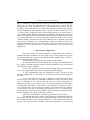
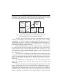
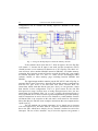
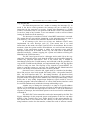
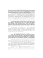
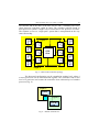
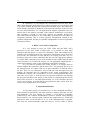
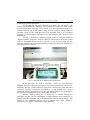
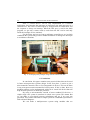
BULETINUL INSTITUTULUI POLITEHNIC DIN IAŞI
Publicat de
Universitatea Tehnică „Gheorghe Asachi” din Iaşi
Tomul LV (LIX), Fasc. 2, 2009
SecŃia
AUTOMATICĂ şi CALCULATOARE
MODERN MICROCONTROLLERS AS VIRTUAL DEVICES
FOR OLD MICROPROCESSOR SYSTEMS
BY
VLAD VASILIU and *ALEODOR DANIEL IOAN
Abstract. The main idea behind this work is to find a way to simplify the
microprocessor based systems. Our solution is to replace all input/output chips (like serial,
parallel, timers, etc.) with a single microcontroller that can have more interconnectivity
capabilities. We can imagine a new kind of virtual I/O devices implemented in
microcontroller by software. This combination of modern microcontroller technology
with old standard microprocessor systems can be effective and powerful for many low
cost industrial control systems. The proposed configuration can offer a new perspective
over the actual research in microprocessor systems which are oriented to industrial control
applications.
Key words: Microcontroller, embedded systems, multi I/O controller, interrupts,
virtual devices.
2000 Mathematics Subject Classification: 68M01, 94C12.
1. Introduction
Very simple microprocessor based systems have a memory block, an
I/O block, a logic part for memory & I/O selection and of course a
microprocessor [1]. The problem to solve is to reduce the complexity, because if
we want a system with serous interconnectivity capabilities we must add some
I/O controllers. That means problems in routing, some problems in
programming, and some problems linked to the dimension of the board. So we
must adopt a new configuration in order to obtain what we want. The main idea
is to remove all I/O hardware controllers, and replacing them with a
microcontroller.
The research started with a simple application for this configuration.
The application is in fact Z80 based micro system [2] with 64Ko+32Ko SRAM
and for I/O part we used a PIC16F877 [3] because this microcontroller is very
40
Vlad Vasiliu and Aleodor Daniel Ioan
easy to connect to a data bus. Even if Z80 is at least 30 years old, it has a very
smart way to solve the interrupts and ZILOG has new versions for this
microprocessor, with capabilities that can be compared with newer devices.
Initially it was intended just to use all on-chip interfaces that PC16F877 had to
replace all hardware I/O controllers (SIO = Serial I/O, PIO = Parallel I/O, CTC
= Counter/Timer Controller) from a classical Z80 system [1], in order to have a
very compact board. When the hardware configuration was defined, it was clear
that the PIC microcontroller can do much more. Because the microprocessor has
a powerful instruction set with sophisticated addressing modes for the large
external memory and because the microcontroller has an internal processing
unit with less capability, but a comprehensive range of peripheral circuits, the
resulted combination can be very useful and effective in a low cost system. All
capabilities will be discussed later, but some hardware issues must be first
understood.
2. Hardware Configuration
The goal beyond the chosen hardware configuration was to build a
modular electronic schematic. So, the whole project was divided in two parts:
the Z80 microprocessor with its own SRAM memory module and a “multi I/O”
interface based on PIC16F877.
The Z80 module contains the following three sub-blocks:
a) The main memory block with the first 32 Kbytes FLASH shadowed
by 32 Kbytes SRAM and the second 32 Kbytes SRAM that can be switched
with another 32 Kbytes SRAM;
b) The logic part that consists in small J-K flip-flops based automaton
with a very simple state machine used for memory blocks paging;
c) The combinational part for decoding I/O ports, because in this
present configuration we can connect a LCD and a tweeter without using the
PIC part.
Even if the Z80 can access only a window of 64 Kbytes at the same
moment [2], we can improvise a method to add more memory. The whole effort
can be explained if we consider that the Z80 has special instructions to
manipulate memory areas. Just because it is an old microprocessor, the number
of instructions that interact with memory is not limited (if we want to create a
very rapid processor we must limit the number of instructions that use memory
or I/O) and, for the Z80 in particular, the instruction set is very powerful [6].
For this project, the solution was to shadow the FLASH memory and to add two
blocks of memory that can be switched by software.
After the system RESET, the memory map looks like in the Fig. 1.
The method that can be used to switch memory configurations after the
next instruction was fetched form the old memory map is very well known by
the old Z80 specialists [2]: the refresh address is a 7 bit value from R (Refresh)
register. This register has 8 bit width so, what about the last bit 7 ? This bit can
Bul. Inst. Polit. Iaşi, t. LV (LIX), f. 2, 2009
41
(and will) be used for memory switching, because the content of the R register
will appear on the address bus only at the end of the fetch memory cycle, after
the next instruction was already extracted from the old configuration.
32Kbytes
FLASH
or
EPROM
0000H
32Kbytes
SRAM0
1st block
0FFFH
32Kbytes
SRAM0
1st block
a
32Kbytes
SRAM1
2nd block
32Kbytes
SRAM2
3rd block
FFFFH
b
Fig. 1 – Memory map after RESET (a) and after the whole program
from FLASH was moved to first block of SRAM (b).
The logic that selects memory blocks was implemented using old style
methods (JK flip-flops and decoders). This logic part can be further
implemented in CPLD (Complex Programmable Logic Devices) but for
“educational” reasons we wanted to be with standard ports and flip-flops [4].
The logic part works like a very small finite automaton with a “state machine”
which tells what memory block is selected.
After system RESET (Fig. 2), the first flip-flop (U2A) is cleared using
the CLR input. Because its QA output also controls the CLR input from the
second flip-flop (U2B), in this way both flip-flops will be cleared to “00”. This
is the initial state, when a EPROM/FLASH memory circuit is selected in the
lower half of memory map and a SRAM0 memory circuit is selected in the
higher half (Fig. 1).
A refresh cycle is initiated when the MREQ (Memory REQuest) signal
becomes low, but only after the RFSH (ReFreSH) signal was already asserted
low [2]. In this moment, the content of the R register will appear on the lower
half of the address bus and the last bit 7 from R will be visible on the A7
address line.
The deactivation of both signals at the end of the refresh cycle will
trigger the flip-flops clock input to allow extra time for address bus
stabilization.
The “00” initial state will remain unchanged how long the A7 bit is still
logical “0” during all refresh cycles. When the A7 bit is changed to logical “1”,
both flip-flops will be set to “11” state, which selects a new memory
configuration: the SRAM0 window will become visible at the lower addresses
and another SRAM1 block will be selected in the higher half of memory map,
instead of SRAM0. The EPROM/FLASH memory cannot be addressed in this
42
Vlad Vasiliu and Aleodor Daniel Ioan
configuration, but its content was already copied to SRAM0 in the initial
configuration.
Fig. 2 – Using two JK flip-flops to control the memory decoder.
If the software then clears the bit 7 from R register, the first flip-flop
will remain “1” because the K input is not used, but the second one will be
cleared because it was connected to function as a “D” flip-flop. The third “10”
state will now select another SRAM2 instead of SRAM1, for further memory
expansion. How long the system will not be reseted, the initial “00” state cannot
be reached anymore. The “10” and “11” states can be interchanged under
software control, to allow memory page switching between SRAM2 and
SRAM1.
The input/output module contains just the PIC16F877 and a flip flop, to
generate WAIT states if necessary, when the Z80 module wants to communicate
with the I/O part. Even if we add some wait states, because there are
instructions which send data blocks (not just a byte), we can generate a burst
data transfer in this configuration. This is a good reason for the old Z80
microprocessor usage, because most of today microprocessors have just two
instructions for I/O transfer (like “in” or “out”). Usually, the microprocessor is
more rapid than the I/O and, to obtain a good computational speed, the memory
and I/O instructions in newer devices were limited to a small number. But the
old known Z80 is an exception to this rule and is well suited for I/O transfer.
More than that, the Z80 has some complex instructions that can compensate the
speed issue [6].
The I/O module can generate interrupts. It is a simple way to interact
with a microprocessor, but more than an “expected” construction can be used
due to the Z80, which has a simpler (let say “unusual”) method to resolve the
interrupts. The use of this “unusual” way to solve the requests can generate a
Bul. Inst. Polit. Iaşi, t. LV (LIX), f. 2, 2009
43
very flexible unit.
The Z80 microprocessor has 3 modes to manage the interrupts [2]. In
mode 0, the device which generates the interrupt can put on data bus any
instruction for the processor to execute. Usually this instruction is a JUMP
(relative or absolute). But we can generate with the PIC 16F877 any instruction
(it can be a jump to any location, or we can transmit a code to execute without
storing the instruction in the memory).
The interrupt is considered “solved” when IRET instruction is executed.
This means that we can send the instruction, or the microprocessor can read it
from memory. Two small issues should be discussed in the following.
In an interrupt cycle, there are at least two hardware WAIT states
implemented for each interrupt cycle [6]. That means that if we send
instructions in this mode, the whole system will be slowed down. But in some
moments, when the system could be slowed down, we can load some interrupts
routines. If the application permits, a whole new interrupt vector with all
interrupts routines can be loaded. In this way, the code will be dynamically
allocated on-the-fly, without stopping the system and without rewriting the
EPROM or the FLASH memory.
The PIC based system can be a debugger and a multi I/O at the very
same time. Practically all the code from the memory can be modified remotely,
without any physical intervention. This is the reason why a method to
interchange between the FLASH memory and a SRAM, with the possibility to
copy all the FLASH into the SRAM, was implemented using a J-K flip-flop that
can be set only one time. The flip-flop is first cleared at system RESET. So,
when we start the system, we can copy the FLASH into the SRAM and after
that we can modify all functions that were written by default.
One more issue is that the M1 signal must be considered at decoding.
Most Z80 projects were built around Z80 family (PIO – the parallel interface,
SIO – the serial interface and CTC – the timing interface). All interfaces from
this family internally decode the M1 signal by construction [7]. The content of
program counter will appear on the address bus at interrupt acknowledge, which
means that if only IORQ (Input/Output ReQuest) signal would be used at
decoding (together with some addresses, of course) then another interface could
be selected simultaneously within the interrupt acknowledge cycle.
Another way to manage the interrupts is to jump to a specific address
(mode 1). The technique isn’t so good to use when we have more I/O devices. A
specific way to solve the interrupt requests is the mode 2. This is the Z80 native
response to interrupts, but in this dual system it can be used well in combination
with mode 0.
The PIC16F877 microcontroller can be also interrupted by the Z80. The
biggest advantage of this proposed system configuration is that we can make
benefit of the “parallel slave port” (PSP) facility of this microcontroller [5].
This means that we can connect the PIC directly to the main processor bus,
using hardware strobes for data transfer, without the need of software control.
44
Vlad Vasiliu and Aleodor Daniel Ioan
For this feature we must sacrifice two ports: PORTD and PORTE. The PORTD
contains all the eight data bits required for the transfer and the PORTE contains
RD (ReaD), WR (WRite) and CS (Chip Select) hardware strobes [8].
Every time when the main processor reads or writes data from or to this
PSP port, an interrupt is automatically generated to the microcontroller central
processing unit. So, it is very easy to interface one of these microcontrollers to a
system with main Z80 microprocessor. Well programmed this device can be
used like a timer, serial port, parallel port, I2C port, SPI port, or we can make
use of the 10 bit integrated ADC or other peripherals that are in this particular
PIC microcontroller (like the EEPROM nonvolatile memory block) [9]. It
should be noted that the Z80 family of peripherals does not contain I2C or
newer standards!
Is obvious that is simpler to interface only one I/O chip instead of three
or four old chips, and more than that, we can set a specific ISR (Interrupt
Service Routine) for each virtual software device. The PIC can transmit any
instruction to the Z80 using mode 0 interrupt response and a newer ISR routine
could be loaded at any time. Using PIC generated instructions, we can change
the position of such routines in the memory and we can make live updates for
them.
The interrupt mode 1 or 2 can be also used. In this case, any ISR could
be loaded with a little help from a boot-loader or an operating system. More
than that, we can create “virtual devices”, because the input and output is in fact
a software function which is called by an ISR when an event appears. In this
way some calculation can be done in parallel.
3. Practical New Multi-Controller Topology
Usually, when we think about a multiprocessor system, most of the time
we have in mind a processor matrix. But we are used to solve problems in a
“divide et impera” algorithm. This kind of algorithm is hard to implement on a
processor matrix and even if implemented, it cannot use all the computational
power. Sometimes, maybe is a better solution to have another structure instead
of connecting some processors to the same bus and try to make it work together.
The main idea behind this “multi-controller” topology is to use the same
functional module connected to a single main master processor which manages
all functions that are implemented in all such functional modules (Fig. 3).
From the hardware point of view, any function or sub-function has the
same structure. That means that behind each block, only one microcontroller
exists and this is linked to another microcontroller with an independent bus.
Only the main processor bus is shared.
When the problem is separated in sub-problems using a “divide at
impera” algorithm, a specific topology will be generated. So, the very same
problem can have two or more specific hardware solutions. In this way, some
production costs can be avoided. Because one microcontroller implements only
Bul. Inst. Polit. Iaşi, t. LV (LIX), f. 2, 2009
45
one function and in the most of the time will be “idle”, something like crosscheck between controllers could be built. The common problem found in
microprocessor systems is higher rate of failure due to the presence of busses.
The solution is to use a “single-pack” system that is encapsulated on the very
same silicon chip.
Sub
function
Sub
function
Sub
function
Function
6
Sub
function
Function
5
CPU
Core
Sub
function
Function
4
Memory
Function
3
Sub
function
Function
2
Sub
function
Function
1
Sub
function
Layer 1
Layer 2
Fig. 3 – Basic multi-controller topology.
The discussed configuration can be extended to another level, where 4
or more processors can be interconnected together. The controllers from a near
level of a processor can become the controllers from a distant layer of another
processor (Fig. 4).
Layer 2
CPU
Cor
Device Layer 2
CPU
Cor
Fig. 4 – Shared virtual device.
46
Vlad Vasiliu and Aleodor Daniel Ioan
In conclusion, we can imagine any construction based on these basic
ideas. More than that, such structures are easy to program, are very intuitive and
very object oriented. Because the construction has more layers, this reduces the
traffic and the possibility of deadlock on the main bus. Because on the CPU bus
we have microcontrollers, we can implement an adaptive algorithm to be sure
that the bus is free when it is needed. If the software architecture is well done,
after releasing a version we can easily improve any module, because the
interaction between modules is very weak and a good interface can reduce all
integration problems. This is a more practical configuration instead of any
parallel configuration, because in a parallel configuration we have a big number
of shared resources.
4. RISC Versus CISC Competition
It is very unusual to have one CISC (Z80) and one RISC (PIC)
processor on the same board. Further more, it is possible to want more
interfaces and that means 2 or more I/O controllers. Then, what should we do
with the time available between two consecutive data frames sent to the ports?
In this time, the controllers are idle and they are waiting new data. So, it is
possible to have one or more controllers that just wait. The appropriate question
is: can the RISC controller process some operations more rapidly than the main
CISC processor? If we know the answer, we can implement something like a
coprocessor and move some of the calculations to the RISC controller.
It is very hard to estimate the results, because it is possible that we
cannot compare the controllers and the main CPU. The proposed idea is to let
the main processor to compete with one or more controllers, to find out who is
the best. This is a very competitive way to find out if the microprocessor can
manage all functions that are integrated in the actual configuration. The
mechanism is simple: call a virtual device to solve a certain problem and in the
same time try to solve it. If the device wins, the microcontroller can interrupt
the processor and deliver the results. If the results are computed quicker by the
main CISC processor, it can mask that interrupt, so, if the controller does not
receive any response, it means that the microprocessor had a result. Next, the
results can be compared for a cross-check.
5. Experimental Results
To test some aspects of virtual devices, we have designed and built a
PCB (Printed Circuit Board), with main processor, memory and only one PIC
microcontroller. The first attempt to emulate a serial RS232 compatible
connection by PIC software and hardware resources, without using interrupt
driven transfer, was well successful. Without any complication, we could send
and receive data via the PIC16F877 to see if the communication is possible.
This first test worked smoothly and after that we tried to make a similar
Bul. Inst. Polit. Iaşi, t. LV (LIX), f. 2, 2009
47
connection, but interrupt driven.
The second test was more difficult to be done. The PIC16F877 was
initially programmed in C language, but a compiled C code is too slow for the
tested configuration (interrupt vector placed in an interrupt acknowledge cycle
without inserting any WAIT states). Only after the function which sends the
interrupt vector to the main processor was rewritten from C to assembler
language, we succeeded to send and receive data using the PIC “virtual” serial
RS232 port.
The Fig. 5 shows how a small text typed on the PC using the Windows
“HyperTerminal” program is sent over RS232 connection to the tested system
and it is displayed exactly on the LCD after it was received using the PIC
internal USART (Universal Synchronous/Asynchronous Receiver/Transmitter)
virtualized by PIC software.
Fig. 5 – Interrupt driven RS232 serial comunication.
In the third test, we tried to virtualize a timer too. We chose the
TIMER1 from PIC: the main processor sends a time constant knowing the PIC
frequency and the virtual controller sends back an interrupt when the timer
overflows. The Fig. 6 shows the waveform of a sound generated by a beeper
connected directly as classic bit I/O to the Z80 main processor. Every change in
the waveform was dictated by the virtual timer overflow.
Another small problem was in witch way we should manage the
interrupts? So, the first test implements a simple software daisy chain but we
realized that any algorithm can be implemented to manage the interrupts. This
feature is very important because we can imagine new, more “adaptive”
algorithms, very hard to implement in other situations.
48
Vlad Vasiliu and Aleodor Daniel Ioan
Now, a “virtual device” can be easy implemented as a software
application. Any function that generates an interrupt to the main processor is a
virtual device. We chose to send request by using normal IO instructions, but
the response is always an interrupt. When the PSP port is read in the main
program, we get only a status word (a result from the PIC can be read only
inside the interrupt service routines).
For the future projects we want to add more controllers to see in which
conditions the system can get into a deadlock and how to manage the interrupts
to avoid these situations.
Fig. 6 – Sound played by a beeper using software timers from PIC.
6. Conclusions
In conclusion, this paper contains some practical ideas that can be used
in future microprocessor systems design. In the first place, is easier to put a
microcontroller instead of four or five integrated I/O devices. This can be done
in any microprocessor/microcontroller based system. If this is done, then very
modular software can be implemented, with a lot of virtual I/O devices that can
help the main processor to finish his job faster.
By using a microcontroller instead of more standard I/O devices, a
simple single core system is transform in a dual core system. This means that
we can make a cross-check between calculations and see if an error was
generated. This feature transforms a simple system in a redundant system that is
able to himself diagnose.
We can make a multiprocessor system using modules that are
Bul. Inst. Polit. Iaşi, t. LV (LIX), f. 2, 2009
49
equivalent from the hardware point of view, but every module can have a
distinctive task to do. For a relative small number of controllers, we can create a
layered structure that can make the integration of all modules in a project much
easier. In this way, we can save time and cost in developing new products.
In the final, a very important aspect must be highlight: the Z80
microprocessor was only a testing choice and any other processor can be used.
Received: February 6, 2009
Continental AG Jassy,
Software Chassis and Safety Department
e-mail: [email protected]
and
*“Gheorghe Asachi” Technical University of Iaşi,
Automatic Control and Applied
Informatics Department
e-mail: [email protected]
REFERENCES
1. Ball S.R., Embedded Microprocessor systems: real world design, 2nd Ed.,
Butterworth-Heinemann, Woburn, 2000.
2. Gaonkar R.M., Z-80 microprocessor: architecture, interfacing, programming, and
design, 3rd edition, Prentice Hall, New Jersey, 2000.
3. Bates M.P., Interfacing PIC Microcontrollers: Embedded Design by Interactive
Simulation, Newnes Elsevier, Oxford, 2006.
4. Mano M. M., Kime C. R., Logic and Computer Design Fundamentals, 3rd Ed.,
Prentice Hall, New Jersey, 2004.
5. Di Jasio L., Wilmshurst T., Ibrahim D., Morton J., Bates M.P., Smith J., Smith D.W.,
Hellebuyck C., PIC Microcontrollers: Know it All, Newnes Elsevier,
Burlington, 2008.
*
6. * * Z80 Family CPU User Manual. User Manual, Zilog Inc.,
www.zilog.com/docs/z80/, 2004.
*
7. * * Z80 Family CPU Peripherals. User Manual, Zilog Inc.,
www.zilog.com/docs/z80/, 2001.
8. *** PICmicro Mid-Range MCU Family, Reference Manual, Microchip Technology
Inc., www.microchip.com, 1997.
9. *** PIC 16F87XA 28/40/44-Pin Enhanced Flash Microcontrollers, Data Sheet,
Microchip Technology Inc., www.microchip.com, 2003.
MICROCONTROLERE MODERNE UTILIZATE CA DISPOZITIVE VIRTUALE
PENTRU VECHILE SISTEME CU MICROPROCESOR
(Rezumat)
Ideea acestei lucrări este găsirea unei metode de simplificare a sistemelor cu
microprocesor. SoluŃia prezentată ar fi înlocuirea tuturor circuitelor de intrare/ieşire
dintr-un sistem clasic cu microprocesor printr-un singur microcontroler modern, care
50
Vlad Vasiliu and Aleodor Daniel Ioan
include deja pe cip o serie întreagă de circuite periferice. Prin implementarea pe
microcontroler a unui software de acces extern la resursele hardware interne, acesta
devine de fapt un circuit virtual de intrare/ieşire pe care microprocesorul principal poate
să-l acceseze în mod transparent, ca şi cum ar fi un set întreg de circuite periferice
hardware văzute printr-un singur port. Un sistem cu microprocesor astfel construit va
avea o structură considerabil simplificată: mai rămân de conectat doar memoriile
principlale şi circuitele de selecŃie ale acestora. Deoarece microprocesorul are un set
puternic de instrucŃiuni cu moduri de adresare sofisticate ale memoriei externe de mari
dimensiuni iar microcontrolerul are o unitate internă de procesare cu capabilităŃi mai
reduse dar o gamă performantă de circuite periferice, combinaŃia rezultată poate fi
foarte utilă şi eficientă în cadrul unor sisteme cu costuri reduse. Ideea lucrării merge mai
departe, considerându-se conectarea mai multor microcontrolere la acelaşi
microprocesor, fiecare implementând o anumită funcŃie de intrare/ieşire sau chiar de
calcul. Mergând în continuare pe această cale, se poate crea chiar un nou tip de
dispozitiv (un dispozitiv virtual), care să fie modelat de o funcŃie dată: se pot diviza şi
împărŃi sarcinile între procesorul principal şi microcontrolere, sistemul căpătând astfel
serioase proprietăŃi de paralelism. ConfiguraŃia hardware propusă poate oferi o
perspectivă nouă asupra cercetărilor legate de sistemele cu microprocesoare orientate cu
precădere spre operaŃii de supervizare şi control industrial.