1
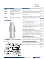
PCI-1712
PCI-1712L
1MS/s, 12-bit High-speed
Multifunction Card
1MS/s, 12-bit High-speed
Multifunction Card w/o AO function
Features
§ PCI-bus mastering for data transfer
§ 16 single-ended, 8 differential or a combination of analog inputs
§ 12-bit A/D converter, with up to 1 MHz sampling rate
§ Pre-, post-, about- and delay-trigger data acquisition modes for analog input
channels
§ Programmable gain for each analog input channel
§ Automatic channel/SD*/BU* scanning
§ Onboard FIFO buffer storing up to 1K samples for A/D and 32K samples for
D/A
§ Two 12-bit analog output channels with continuous waveform output function
§ Auto calibration of analog input and output channels
§ 16 digital input and output channels
§ Three 16-bit programmable multifunction counter/timers on 10 MHz
PCLD-8712
PCI-17112/1712L
Introduction
The PCI-1712/1712L is a powerful high-speed multifunction card for the PCI bus. It features a 1 MHz 12-bit A/D converter, an onboard FIFO buffer (storing up to 1 K samples for A/D,
and up to 32 K samples for D/A conversion). The PCI-1712 provides a total of up to 16 single-ended or 8 differential A/D input channels or a mixed combination, two 12-bit D/A output
c c functions for different user requirements:
Specifications
Analog Output
Analog Input
Channels
Resolution
16 Single-Ended or 8 Differential or Combination
FIFO Size
12-bit
1 K samples
Multi-channel, single gain: 1 MS/s
Multi-channel, multi gain: 600 KS/s
Multi-channel, multi gain, unipolar/bipolar: 400 KS/s
Common mode
±11 V max.
500 ns
voltage
(operational)
Max. Sampling
Rate
Conversion Time
Gain
Input range and
Gain List
1
2
4
Small Signal
Bandwidth for PGA
Max. Input voltage
Input Impedance
N/A
0 ~ 10
0~5
0 ~ 2.5 0 ~ 1.25
±10
±5
±2.5
±1.25
±0.625
0.5
1
2
4
8
±80
±30
±30
±30
±30
±30
±30
±30
±30
±30
0.5
1
2
4
8
4.0 MHz 4.0 MHz 2.0 MHz 1.5 MHz 0.65 MHz
Input Protect
30 Vp-p
100W 10pF (Off); 100W 100pF (On)
Software, On-board Programmable Pacer or External,
Pre-trigger, Post-trigger, Delay-trigger, About-trigger
DNLE: ±1LSB; INLE: ±1LSB; Offset error < 1LSB
Gain
0.5
1
2
4
8
Gain Error:
0.15
0.03
0.03
0.05
0.1
(% FSR)
SNR: 68 dB; ENOB: 11 bits; THD: -75 dB typical
Trigger Mode
DC
AC
Digital Input /Output
Input
Channels
Input
Voltage
Note:
5-14
16
Low
Low
0.8 V max.
0.5 V max. @+24
mA (sink)
Number of
ports
High
High
2 (8-ch/port)
2.0V min.
2.4 V min. @ -15 mA
(source)
The sampling rate depends on the computer hardware architecture and software
environment. The rates may vary due to programming language, code efficiency,
CPU utilization and more.
Plug-in DA&C Cards
Output Range
(Internal & External
Reference)
Accuracy
8
Unipolar
Bipolar
Gain
Zero (µV/° C)
Gain (ppm/° C)
Gain
Bandwidth
±20 V
Drift
Accuracy
0.5
Channels
Resolution
Operation mode
Offset
Drift
Max. Transfer Rate
Output Impedance
settling Time
2
12-bit
32 K samples
FIFO Size
Single output, continuous output, waveform output
Using Internal
0 ~ +5 V, 0 ~ +10 V, -5 ~ +5 V, -10 ~ +10 V
Reference
0 ~ +x V @ +x V (-10 ≤ x ≤ 10)
Using External
Reference
-x ~ +x V @ +x V (-10 ≤ x ≤ 10)
Relative
±1 LSB
Differential
±1 LSB (monotonic)
Non-linearity
<1 LSB
20 V/µs
Slew Rate
Driving Capability
10 ppm/° C
±10 mA
Single Channel: 1 MS/s max. for FSR
Dual Channel: 500 KS/s max. for FSR
0.1 Ω max.
5 MHz
Max. Digital Update Rate
2 µs (to ±1/2 LSB of FSB)
Counter/Timer
Channels
TTL level
Compatibility
BASE Clock
Clock Input
Gate Input
Counter
Low
Low
Low
3
Resolution
Max. Input Frequency
10 MHz, 1 MHz, 100 KHz, 10 KHz
0.8 V max.
0.8 V max.
0.5 V max. @ +24 mA
High
High
High
16-bit
10 MHz
2.0 V min.
2.0 V min.
2.0 V min. @ -15 mA
General
I/O Connector Type
68-pin SCSI-II female
Dimensions
175 mm x 100 mm (6.9” x 3.9”)
Power Consumption
Temperature
Typical
+5 V @ 850 mA; +12 V @ 600 mA
Max.
+5 V @ 1 A; +12 V @ 700 mA
Operation
0 ~ +60° C (32 ~ 140° F)
(refer to IEC 68-2-1, 2)
Storage
-20 ~ +85° C (-4 ~ 185° F)
Relative Humidity
5 ~ 95 % RH non-condensing (refer to IEC 68-2-3)
Certification
CE certified
PCI-1712
PCI-1712L
Ordering Information
§ PCI-1712
§ PCI-1712L
§ PCLD-8712
§ PCL-10168
§ ADAM-3968
Feature Details
1MS/s, 12-bit High-speed Multifunction Card, user’s
manual and driver CD-ROM. (cable not included)
1MS/s, 12-bit High-speed Multifunction Card w/o
AO, user’s manual and driver CD-ROM. (cable not
included)
Industrial Wiring Terminal Board for DIN-rail mounting.
(cable not included)
68-pin SCSI-II cable with male connectors on both
ends and special shielding for noise reduction, 1 and 2
m
68-pin SCSI-II Wiring Terminal Board for DIN-rail
Mounting
Pin Assignment
PCI-bus Mastering Data Transfer
1
2
3
4
5
6
7
8
9
10
11
12
13
14
15
16
IPPC & AWS
The PCI-1712/1712L supports PCI-Bus mastering DMA for high-speed data transfer and
gap-free analog input and analog output. By setting aside a block of memory in the PC, TPC
the PCI-1712/1712L performs bus-mastering data transfers without CPU intervention,
setting the CPU free to perform other more urgent tasks such as data analysis and graphic
manipulation. The function allows users to run all I/O functions simultaneously at full
FPM
speed without losing data.
Plug-and-play Function
The PCI-1712/1712L is a Plug-and-Play device, which fully complies with the PCI ATM
Specification Rev 2.2. During card installation, you have no need to set any jumpers
or DIP switches. Instead, all bus-related configurations such as base I/O address and
interrupt are automatically done by the Plug-and-Play function.
On-board FIFO Memory
DA&C
The PCI-1712/1712L provides an on-board FIFO (First In First Out) memory buffer, storing
up to 1K samples for A/D and 32K for D/A conversion (PCI-1712 only).
cPCI
Automatic Channel/Gain/SD*/BU* Scanning
PCI-1712/1712L features an automatic channel/Gain/SD/BU scanning circuit. This circuit
controls multiplexer switching during sampling in a way that is much more efficient than ADAM-3000
software implementation. Onboard SRAM stores different gain, SD and BU values for
each channel. This combination lets users perform multi-channel high-speed sampling
with different gain, SD and BU values for each channel.
eConnectivity
SD: Single-Ended/Differential; BU: Bipolar/Unipolar
Flexible Triggering and Clocking Capabilities
ICOM
The PCI-1712/1712L provides flexibility in triggering action, both in the available trigger
modes and trigger events for analog input. You can acquire data using post-trigger,
pre-trigger, delay-trigger and about-trigger modes. The trigger source could be either an
Software
analog or digital signal. The analog trigger could originate from a dedicated input pin.
In fact, you can designate any of the analog input channels as the analog trigger input.
You can set the analog trigger level within a voltage range from zero to A/D FSR. With
the trigger signal being digital, you can pace A/D and D/A conversion using software UNO-2000/3000
interrupt, internal or external clock.
Continuous Analog Output (PCI-1712 only)
VBOX
The PCI-1712 provides two analog output channels. Both of them can perform continuous
waveform output. The analog output can be up to 500 kS/s for each analog output channel.
Or you can load a cyclic waveform into an onboard FIFO, which will continuously output
the cyclic waveform. The onboard FIFO of the PCI-1712 can store 2 to 32K samples of ADAM-4000
the waveform.
Block Diagram
On-board Programmable Multifunction Counter/Timer
ADAM-5000
The PCI-1712/1712L is equipped with 3 programmable multifunction counter/timers,
which can serve as a pacer trigger for A/D conversion. The counter chip is an 82C54
or equivalent, which incorporates three 16-bit channels on a 10 MHz clock. And then
we enhance the gate and clock input function for more applications, of event counting, ADAM-6000
pulse generation, duty cycle frequency generation, one shot, frequency measurement
and pulse width measurement.
ADAM-8000
Online Download www.interwld.com
5-15