1
Heurikon HK681M120
User's Manual
HElRIK9N
Microcomputers For Industry
Heurikon HK68/M120 - User's Manual
Heurikon Corporation
Madison, WI
INTRODUCTION •••••••••••••••••••••••••••••••••••••••••••••••••••••
1.1
Disclaimer •••••••••••••••••••••••••••••••••••••••••••••••••
1
2.
HK68/M120 FEATURE SUMMARy ••••••••••••••••••••••••••••••••••••••••
2
3.
BLOCK DIAGRAM ••••••••••••••••••••••••••••••••••••••••••••••••••••
4
4.
GETTING GOING ••••••••••••••••••••••••••••••••••••••••••••••••••••
Installation Steps •••••••••••••••••••••••••••••••••••••••••
4.1
Troubleshooting and Service Information ••••••••••••••••••••
4.2
Monitor Summary ••••••••••••••••••••••••••••••••••••••••••••
4.3
5
5
6
7
5.
MPU SUMMARY INFORMATION.eeeee....................................
MPU Interrupts.............................................
5.1
MPU Exception Vectors......................................
5.2
Status LEDs................................................
5.3
5.4
8
8
12
1.
6.
DMAC
6.1
1
8
SUPPORT..................................................... 13
DMA Software Implementation Example........................
14
7.
FLOATING POINT CO-PROCESSOR (FPP) ••••••••••••••••••••••••••••••••
7.1
FPP Feature Summary ••••••••••••••••••••••••••••••••••••••••
7.2
FPP Bypass •••••••••••••••••••••••••••••••••••••••••••••••••
17
17
17
8.
MEMORY MANAGEMENT CO-PROCESSOR (PMMU) ••••••••••••••••••••••••••••
Function Code Definitions ••••••••••••••••••••••••••••••••••
8.1
PMMU Address Line Block Diagram ••••••••••••••••••••••••••••
8.2
PMMU Bypass ••••••••••••••••••••••••••••••••••••••••••••••••
8.3
Alternate Capabilities - MMB •••••••••••••••••••••••••••••••
8.4
18
18
19
20
20
9.
SYSTEM ERROR HANDLING ••••••••••••••••••••••••••••••••••••••••••••
Error Conditions •••••••••••••••••••••••••••••••••••••••••••
9.1
21
21
10.
ON-CARD MEMORY CONFIGURATION •••••••••••••••••••••••••••••••••••••
23
23
10.1
ROM ••••••••••••••••••••••••••••••••••••••••••••••••••••••••
10.1.1 8-bit Data Path 23
10.1.2 32-bit Data Path 24
10.2 On-Card RAM ••••••••••••••••••••••••••••••••••••••••••••••••
10.3 On-card Memory Sizing ••••••••••••••••••••••••••••••••••••••
10.4 Bus Memory •••••••••••••••••••••••••••••••••••••••••••••••••
10.5 Physical Memory Map ••••••••••••••••••••••••••••••••••••••••
10.6 Memory Timing ••••••••••••••••••••••••••••••••••••••••••••••
10.7 Non-Volatile RAM •••••••••••••••••••••••••••••••••••••••••••
i
26
27
27
29
30
32
MULTIBUS CONTROL •••••••••••••••••••••••••••••••••••••••••••••••••
11.1 Bus Control Signals ••••••••••••••••••••••••••••••••••••••••
11.1.1 PI, Primary System Bus 33
11.1.2 P2, Expansion Bus 35
11.2 On-card going off (TO the Multibus) ••••••••••••••••••••••••
11.3 Off-card coming on (FROM the bus) ••••••••••••••••••••••••••
11.4 Bus Map (Slave Mode} •••••••••••••••••••••••••••••••••••••••
11.5 Bus Interrupts •••••••••••••••••••••••••••••••••••••••••••••
11.6 Bus Data Conventions •••••••••••••••••••••••••••••••••••••••
11.7 Watchdog Timer •••••••••••••••••••••••••••••••••••••••••••••
11.8 Mailbox ••••••••••••••••••••••••••••••••••••••••••••••••••••
11.9 Relevant Jumpers - Bus Control •••••••••••••••••••••••••••••
42
12.
MISCELLANEOUS DEVICES ••••••••••••••••••••••••••••••••••••••••••••
12.1 User Jumper Input Port •••••••••••••••••••••••••••••••••••••
12.2 User LEDs ••••••••••••••••••••••••••••••••••••••••••••••••••
46
46
46
13.
CIO USAGE ••••••••••••••••••••••••••••••••••••••••••••••••••••••••
13.1 Port A Bit Definition ••••••••••••••••••••••••••••••••••••••
13.2 Port B Bit Definition ••••••••••••••••••••••••••••••••••••••
13.3 Port C Bit Definition ••••••••••••••••••••••••••••••••••••••
13.4 Counter/Timers •••••••••••••••••••••••••••••••••••••••••••••
13.5 Register Address Summary (CIO} •••••••••••••••••••••••••••••
13.6 CIO Initialization •••••••••••••••••••••••••••••••••••••••••
13.7 CIO Programming Hints ••••••••••••••••••••••••••••••••••••••
47
47
47
11.
33
33
36
37
38
38
39
40
40
48
48
48
49
51
14.
SERIAL I/O •••••••••••••••••••••••••••••••••••••••••••••••••••••••
14.1 RS-232 Pinouts •••••••••••••••••••••••••••••••••••••••••••••
14.2 Signal Naming Conventions (RS-232) •••••••••••••••••••••••••
14.3 Connector Conventions ••••••••••••••••••••••••••••••••••••••
14.4 Port Address Summary •••••••••••••••••••••••••••••••••••••••
14.5 RS-422 Operation •••••••••••••••••••••••••••••••••••••••••••
14.6 Relevant Jumpers (Serial I/O) ••••••••••••••••••••••••••••••
14.7 Serial I/O Cable Drawing •••••••••••••••••••••••••••••••••••
52
52
53
55
56
57
57
58
15.
SCSI PORT ••••••••••••••••••••••••••••••••••••••••••••••••••••••••
15.1 SCSI Implementation Notes ••••••••••••••••••••••••••••••••••
15.2 Register Address Summary (SCSI} ••••••••••••••••••••••••••••
15.3 SCSI Port Pinouts ••••••••••••••••••••••••••••••••••••••••••
59
59
60
60
16.
CENTRONICS PORT ••••••••••••••••••••••••••••••••••••••••••••••••••
16.1 Centronics Port Configuration ••••••••••••••••••••••••••••••
16.2 Control Port Addresses - Centronics ••••••••••••••••••••••••
16.3 Centronics Printer Interface Cable •••••••••••••••••••••••••
61
61
62
64
17.
SBX EXPANSION I/O INTERFACE ••••••••••••••••••••••••••••••••••••••
17.1 SBX Connector Pin Assignments ••••••••••••••••••••••••••••••
17.2 Device Address Summary (SBX) •••••••••••••••••••••••••••••••
17.3 SBX Module ID Codes ••••••••••••••••••••••••••••••••••••••••
65
65
65
67
18.
REAL-TIME CLOCK (RTC) - Optional Feature •••••••••••••••••••••••••
68
- ii -
19.
MULTIBUS INTERFACE •••••••••••••••••••••••••••••••••••••••••••••••
19.1 PI (Multibus) Pin Assignments ••••••••••••••••••••••••••••••
19.2 P2 (iLBX) Pin Assignments ••••••••••••••••••••••••••••••••••
19.3 Multibus Compliance Levels •••••••••••••••••••••••••••••••••
19.4 Power Requirements •••••••••••••••••••••••••••••••••••••••••
19.5 Mechanical Specifications ••••••••••••••••••••••••••••••••••
20.
SUID1ARY INFORMATION ••••••••••••••••••••••••••••••••••••••••••••••
74
Software Initialization Summary ••••••••••••••••••••••••••••
On-Card I/O Addresses ••••••••••••••••••••••••••••••••••••••
Hardware Configuration Jumpers •••••••••••••••••••••••••••••
74
76
21.
READER COMMENT FORM ••••••••••••••••••••••••••••••••••••••••••••••
79
22.
APPENDICES •••••••••••••••••••••••••••••••••••••••••••••••••••••••
22.1 Additional Technical Literature ••••••••••••••••••••••••••••
22.2 HK68 Family - Feature Summary ••••••••••••••••••••••••••••••
80
80
80
23.
INDEX ••••••••••••••••••••••••••••••••••••••••••••••••••••••••••••
81
20.1
20.2
20.3
- iii -
71
71
72
73
73
73
75
LIST OF FIGURES
Figure 1.
HK68/M120 Block Diagram...................................
4
Figure 2.
DMA Software Implementation Example {Part 1)..............
14
Figure 3.
DMA Software Implementation Example {Part 2)..............
15
Figure 4.
DMA
3)..............
16
Figure 5.
MPU Accesses to Memory or Bus.............................
19
Figure 6.
HK68/M120 Physical Memory Map.............................
29
Figure 7.
Memory Accesses from Multibus.............................
37
Figure 8.
Sample Mailbox Interrupt Service Routine..................
42
Figure 9.
Bus Data Interface - Logic Diagram........................
45
Figure 10.
CIO Program Example {C Portion) •••••••••••••••••••••••••••
50
Figure 11.
CIO Program Example (Assembly Code Portion) •••••••••••••••
50
Figure 12.
Serial I/O Cable Drawing ••••••••••••••••••••••••••••••••••
58
Figure 13.
Centronics Interface - Block Diagram ••••••••••••••••••••••
63
Figure 14.
Centronics Printer Interface Cable ••••••••••••••••••••••••
64
Figure 15.
Real-Time Clock, Example Software •••••••••••••••••••••••••
69
Figure 16.
Jumper Locations •••••••••••••••••••••••••••••••••••••••••
77
Software Implementation Example {Part
- iv -
LIST OF TABLES
Table 1.
MPU Interrupt Levels.......................................
8
Table 2.
MPU Exception Vectors......................................
9
Table 3.
Suggested Interrupt Vectors ••••••••••••••••••••••••••••••••
10
Table 4.
Device Interrupt Vector Values (Suggested) •••••••••••••••••
11
Table 5.
Status LEDs (P5) •••••••••••••••••••••••••••••••••••••••••••
12
Table 6.
Control Panel Interface (P5) •••••••••••••••••••••••••••••••
12
Table 7.
68020 Coprocessor 10 Codes •••••••••••••••••••••••••••••••••
12
Table 8.
Pseudo-DMAC Capabilities •••••••••••••••••••••••••••••••••••
13
Table 9.
Function Code Assignments ••••••••••••••••••• ~~~~~~~~~~~~~~~
18
Table 10.
PMMU Bypass Connections ••••••••••••••••••••••••••••••••••••
20
Table 11.
MMB Registers ••••••••••••••••••••••••••••••••••••••••••••••
20
Table 12.
ROM Jumpers, 8-bit Data Path •••••••••••••••••••••••••••••••
23
Table 13.
ROM Address Translation, 8-bit Data Path •••••••••••••••••••
24
Table 14.
ROM Chip Positions (32-bit Data Path) ••••••••••••••••••••••
24
Table 15.
ROM Capacity and Jumper Positions (32-bit Data Path) •••••••
25
Table 16.
Memory Control Word Bit definitions ••••••••••••••••••••••••
26
Table 17.
On-card RAM Size Selection •••••••••••••••••••••••••••••••••
26
Table 18.
On-card RAM Capacity •••••••••••••••••••••••••••••••••••••••
27
Table 19.
Bus Selection Control Bit definitions ••••••••••••••••••••••
28
Table 20.
On-card Memory Cycle Timing (RAM) ••••••••••••••••••••••••••
30
Table 21.
Relative MPU/RAM Performance Figures •••••••••••••••••••••••
31
Table 22.
Non-Volatile RAM Addresses •••••••••••••••••••••••••••••••••
32
Table 23.
NV-RAM Contents (partial) ••••••••••••••••••••••••••••••••••
32
- v -
Table 24.
Bus Control Bits •••••••••••••••••••••••••••••••••••••••••••
36
Table 25.
Bus Control Bit Addresses ••••••••••••••••••••••••••••••••••
36
Table 26.
Bus Map - Off-card Coming
On •••••••••••••••••••••••••••••••
38
Table 27.
Multibus Byte Ordering Conventions •••••••••••••••••••••••••
39
Table 28.
Bus Mapping PLE (M120-MAP-oO) ••••••••••••••••••••••••••••••
41
Table 29.
Mailbox PLE (U80 Pin Allocations •••••••••••••••••••••••••••
41
Table 30.
Bus Control Jumpers ••••••••••••••••••••••••••••••••••••••••
42
Table 31.
Multibus Convention Logic
Key for Table 32 •••••••••••••••
43
Table 32.
Multibus Convention Logic - Detail •••••••••••••••••••••••••
45
Table 33.
User Jumpers
Bit Definitions •••••••••••••••••••••••••••••
46
Table 34.
User Jumpers - Input States ••••••••••••••••••••••••••••••••
46
Table 35.
User LEDs - Addresses ••••••••••••••••••••••••••••••••••••••
46
Table 36.
CIO Port A Bit Definitions •••••••••••••••••••••••••••••••••
47
Table 37.
CIO Port B Bit Definitions •••••••••••••••••••••••••••••••••
47
Table 38.
CIO Port C Bit Definitions •••••••••••••••••••••••••••••••••
48
Table 39.
CIO Register Addresses •••••••••••••••••••••••••••••••••••••
48
Table 40.
Serial Port A Pinouts ••••••••••••••••••••••••••••••••••••••
52
Table 41.
Serial Port B Pinouts ••••••••••••••••••••••••••••••••••••••
53
Table 42.
Signal Naming Conventions ••••••••••••••••••••••••••••••••••
54
Table 43.
RS-232 Cable Reversal ••••••••••••••••••••••••••••••••••••••
54
Table 44.
DUSCC Register Addresses •••••••••••••••••••••••••••••••••••
56
Table 45.
RS-422 Header Wiring •••••••••••••••••••••••••••••••••••••••
57
Table 46.
Relevant Jumpers - Serial I/O •••••••••••••••••••••••••••••
57
Table 47.
SCSI Register Address Summary ••••••••••••••••••••••••••••••
60
Table 48.
SCSI Pinouts •••••••••••••••••••••••••••••••••••••••••••••••
60
Table 49.
Centronics Pinout (Connector P3) •••••••••••••••••••••••••••
61
vi
Table 50.
Centronics Control Addresses •••••••••••••••••••••••••••••••
62
Table 51.
Centronics Data/Status Addresses •••••••••••••••••••••••••••
62
Table 52.
SBX Connector Pinout (P7) ••••••••••••••••••••••••••••••••••
65
Table 53.
SBX Address Summary
8-bit Modules ••••••••••••••••••••••••
66
Table 54.
SBX Address Summary - 16-bit Modules •••••••••••••••••••••••
66
Table 55.
Heurikon SBX Module ID Codes •••••••••••••••••••••••••••••••
67
Table 56.
RTC module, physical effects •••••••••••••••••••••••••••••••
68
Table 57.
PI (Multibus) Connector Pinout •••••••••••••••••••••••••••••
72
Table 58.
P2 (iLBX) Pin Assignments ••••••••••••••••••••••••••••••••••
73
Table 59.
Power Requirements •••••••••••••••••••••••••••••••••••••••••
73
Table 60.
Mechanical Specifications ••••••••••••••••••••••••••••••••••
73
Table 61.
.Address
J •• • •• • • • ••• • • • • • • • • • • • • •• • ••••••••••••••••••
75
Table 62.
Jumper Summary •••••••••••••••••••••••••••••••••••••••••••••
76
Table 63.
Additional Technical Literature ••••••••••••••••••••••••••••
80
Table 64.
HK68 Family Feature Summary ••••••••••••••••••••••••••••••••
80
C""Ift't.ft'ln.-TP
U\.A.I.U.lUQ..&..
vii
Heurikon HK68/M120 - User's Manual
INTRODUCTION
1
1.
1
INTRODUCTION
The purpose of this manual is to document the features of the Heurikon
HK68/M120 (tm) microcomputer board.
This manual covers the unique features of the HK68/M120 board. Although
general information, such as MPU, MMU, SCSI, CIO, and DUSCC programming is
discussed, more detailed information is available directly from the chip
manufacturers.
Feel free to contact Heurikon Corporation (Customer Support Department) if
questions arise. We are prepared to answer general questions as well as
help with specific applications.
1.1
Disclaimer
The information in this manual has been checked and is believed to be
accurate and reliable. HOWEVER, NO RESPONSIBILITY IS ASSUMED BY HEURIKON
FOR ITS USE OR FOR ANY INACCURACIES. Specifications are subject to change
without notice. HEURIKON DOES NOT ASSUME ANY LIABILITY ARISING OUT OF USE
OR OTHER APPLICATION OF ANY PRODUCT, CIRCUIT OR PROGRAM DESCRIBED HEREIN.
This document does not convey any license under Heurikon's patents or the
rights of others.
1 HK68, HK68/M120 and Hbug-Ml20 are trademarks of Heurikon Corporation.
2 This document was prepared using the UNIX nroff facility and the
PWB/mm macros.
3 UNIX is a trademark of AT&T Bell Laboratories.
Copyright 1987
Heurikon Corporation
Madison, WI
Heurikon HK68/M120 - User's Manual
HK68/M120 FEATURE SUMMARY
2
2.
2
HK68/M120 FEATURE SUMMARY
MPU
Motorola 68020 microprocessor chip; 12.5 Mhz; 16.67, 20 and
25 Mhz option; 32-bit internal architecture, 32-bit address
and data paths; 32 address lines; 4 gigabyte addressing
range; 256-byte Instruction Cache. (Ref: section 5)
FPP
68881 Floating Point Co-processor.
P754 Binary Floating Point Standard.
PMMU
Motorola 68851 chip (or equiv).
Provides logical to
physical address translation. Demand Paged Virtual Memory
operation.
(Ref:
section 8)
(Not present on the
HK68/M12F.)
RAM
256K to 4 megabyte capacity; One parity bit per byte; Uses
64K, 256K or 1024K x 9 DRAMs.
Hardware refresh. (Ref:
section 10)
EPROM
Four ROM sockets; 256 Kbyte total. capacity.
data path. (Ref: section 10)
Multibus
24-bit addressing (16 megabyte range); 16-bit data bus,
compatible with 8-bit boards; Eight bus interrupts, bidirectional (via CIO); Master/Slave modes; On-card byte
swap buffer. (Ref: section 11)
iLBX bus
High speed local memory expansion up to 16 Mbytes; Supports
a secondary bus master. (Ref: section 11)
Serial I/O
Two serial I/O ports (Signetics 68562 Serial Communication
Controller - DUSCC); Separate baud rate generators for each
port;
Asynchronous
and
synchronous
modes;
RS-232C
interface, RS-422 option. (Ref: section 14)
SCSI
ANSI X3T9.2 compatible SCSI controller; supports up to 8
disk drive controllers or other devices; (Ref: section 15)
Centronics
Control I/F and eight-bit output port for Centronics-type
printer. (Ref: section 16)
LEDs
Four user LEDs under software control; Four MPU/BUS status
LEDs (Ref: section 12)
User Jumpers
Eight user definable jumpers.
(Ref: section 12)
SBX
One 16-bit SBX connector;
expansion. (Ref: section 17)
provides
CIO
Zilog Z8536 Counter/Timer and Parallel I/O Unit; three 16bit counter/timers; three parallel ports for on-card
Copyright 1987
Heurikon Corporation
Implements the IEEE(Ref: section 7)
I/O
8 or 32 bit
or
feature
Madison, WI
3
Heurikon HK68/M120 - User's Manual
HK68/M120 FEATURE SUMMARY
control functions.
3
(Ref: section 13)
NV-RAM
Nonvolatile Static RAM; 256 x 4 configuration; Internal
EEpROM; 100 year retention; 10,000 store cycle lifetime;
For user definable functions. (Ref: section 10.7)
Mailbox
Allows remote interrupt of the HK68/M120
Multibus addresses. (Ref: section 11.8)
RTC
Optional
Real-Time
Clock
module
for
time-of-day
maintenance. With battery backup. (Ref: section 18)
Copyright 1987
Heurikon Corporation
via
specified
Madison, WI
Heurikon HK68/M120 - User's Manual
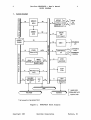
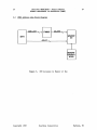
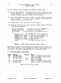
BLOCK DIAGRAM
4
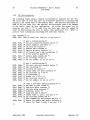
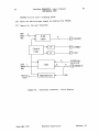
3.
4
BLOCK DIAGRAM
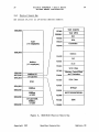
--....,,,
po--
r--('of
M
~
68020
32
,.
..
MPU
co
..
32
~
r
"..
68562
(2 porb)
a
Baud R.1Iteo
r
(J)
(J)
Geoneor' ator's
RS
232
Ilf
w
HJ
H
SERIAL
1/0
PORTS
a:::
0
0
-<
-.J
-<
68881
C)
32
r'"'"
FPP
~
r
'
....
8
Z8536
_....
cia
r
0
(3 T1 mers)
V
68851 *
.
32
r
I"
PMMU
..
....
I
.
16
.
SBX 1
J
='
m
II
('of
M
i
18
-.....,
..
r
I;;
i
EPROM
256K BYTES
8/32
-<
-<
w'-
~
0
('of
("CNTRn .. , ,("e-
~ ~A;~"WV
~ CENTRON ICS
~:J CONTROL
CENTRONICS
Ilf
8
t-
U)
EXPANS.ION
110
--
r
(J)
='
m
U)
U)
22
DRAM
CONTROLLER
w
a:::
0
0
DRAM
4 MBVTES
.",
A
USER
JUMPERS
8
PARITY LOGIC
-<
...J
-<
~
4
(/)
>:x:
8
0..
r
24 . .
NON-VOLATILE
RAM
MAILBOX
MUL TlBUS
Ilf
~.
..
Lo
16 ..
..
iI
r
I/F
'-
8
'---
I
ILBX
)
MULTIBUS
USER
LED~
r
ILBX
'"
~
y
4
,
SCSI
CONTROLLER
'w'D33C93
"
.,.
SCSI BUS
)
~
HARD DISK
STREAMER TAPE
flOPPY DISK
* Not present on the HK68/M 12f
Figure 1.
Copyright 1987
HK68/M120 Block Diagram
Heurikon Corporation
Madison. WI
Heurikon HK68/M120 - User's Manual
GETTING GOING
5
4.
5
GETTING GOING
Here is what you need to get the Heurikon HK68/M120 "on-the-air 1f :
• Heurikon HK68/M120 Microcomputer board
• Card cage and power supply
• Serial I/F cable (RS-232)
• CRT Terminal
~
4.1
Heurikon Hbug-M120 monitor and bootstrap EPROM
Installation Steps
• CAUTION: All semiconductors should be handled with care.
Static
discharges can easily damage the components on the HK68/M120. Keep
the board in an anti-static bag whenever it is out of the system
chassis and do not handle the board unless absolutely necessary.
Ground your body before touching the HK68/M120 board.
High operating temperatures will cause unpredictable
• CAUTION:
operatione Because of the high chip density, fan cooling is required
for most configurations, even when cards are placed on extenders.
All products are fully tested before they are shipped from the factory.
When you receive your HK68/MI20, follow these steps to assure yourself
that the system is operational:
[1]
Visually inspect the board(s) for loose components which could be
the result of shipping vibrations. Visually inspect the chassis and
all cables. Be sure all boards are seated properly in the card cage.
Be sure all cables are securely in place.
[2]
Connect a CRT terminal to Serial Port B, via connector P6. If you
are making your own cables, refer to section 14. Set the terminal
as follows:
• 9600 baud, full duplex.
• Eight data bits (no parity).
• Two stop bits for transmit data.
• One stop bit for receive data.
• If your terminal does not have separate controls for transmit
and receive stop bits, select one stop bit for both transmit
and receive.
Copyright 1987
Heurikon Corporation
Madison, WI
Heurikon HK68/M120 - User's Manual
GETTING GOING
6
6
[3]
Connect AC power and turn the system on.
[4]
Push the system RESET button. A sign-on message and prompt from the
monitor should appear on the screen.
If not, check your power
supply voltages and CRT cabling.
[5]
Now is the time to read the monitor manual and the operating system
literature. Short course: To boot the operating system, insert a
diskette and enter 'bf' (for boot floppy) or 'bw' (to boot from
Winchester.)
[6]
Reconfigure the jumpers, etc, as necessary for your application.
See Section 20 for a summary of I/O device addresses and
configuration jumpers.
4.2
Troubleshooting and Service Information
In case of difficulty, use this checklist:
[1]
Be sure the system is not overheating.
[2]
Inspect the power cables and connectors. If the HK68/M120 board has
power, one of the four status LEDs (near P4) should be on.
[3]
If the Hbug-Ml20 monitor program is executing, run the diagnostics,
via command 'uc' or 'um'.
[4]
Check your power supply for proper DC voltages. If possible, look
for excessive power supply ripple or noise using an oscilloscope.
[5]
Check the chips to be sure they are firmly in place. Look for chips
with bent or broken pins. In particular, check the EPROMs.
[6]
Check your terminal switches and cables. Be sure the P6 connector
is on properly. The cable stripe (wire #1) should be toward the
center of the HK68/M120 board and the cable should flow toward the
rear. The port B portion of the cable is on the pin #34 side. If
you have made your own cables, pay particular attention to the cable
drawings in section 14.
[7]
Check the jumpers to be sure your board is configured properly. All
jumpers should be in the "standard configuration" positions shown in
section 20.3.
[8]
Mter you have checked all of the above items, call us at (608)271-8700 and ask our Customer Service Department for help. Please
have the following information handy:
~
The state of the Status LEDs (near P4).
Copyright 1987
Heurikon Corporation
Madison, WI
Heurikon HK68/M120 - User's Manual
GETTING GOING
7
7
~
The monitor program revision level (part of sign=on message).
~
The HK68/M120 p.c.b. serial number (scribed along card edge).
~
The complete HK68/M120 model number, including option codes.
~
The serial number of the Operating System.
If you plan to return the board to Heurikon for service, contact our
Customer Service Department to obtain a Return Merchandise
Authorization (RMA)-number. Be prepared to provide the items listed
above, plus your Purchase Order number and billing information if
your h~68/M120 is out of warranty. If you return the board, be sure
to enclose it in the anti-static bag, such as the one in which it
was originally shipped. Send it prepaid to:
Heurikon Corporation
Factory Service Department
3201 Latham Drive
Madison, WI 53713
Please put the RMA number on the
problem most efficiently.
4.3
package so we can handle your
Monitor Summary
The HK68/M120 monitor and bootstrap program, Hbug-MI20, is contained in
one EPROM. It is intended to provide a fundamental ability to check the
memory and I/O devices, to manually enter a program and to down-line load
or bootstrap a larger program into memory.
Advanced features and
utilities may be loaded from media or via an operating system.
Refer to the Hbug-M120 manual for details on the commands and command
formats.
Copyright 1987
Heurikon Corporation
Madison, WI
Heurikon HK68/M120 - User's Manual
MPU SUMMARY INFORMATION
8
5.
8
MPU SUMMARY INFORMATION
This section details some of the important features of the 68020 MPU chip
and, in particular, those items which are specific to the implementation
on the Heurikon HK68/M120.
5.1
MPU Interrupts
The MPU can internally set an interrupt priority level in such a way that
interrupts of a lower priority will not be honored.
Interrupt level
seven, however, cannot be masked off.
Level
7
6
5
4
3
2
1
o
Interrupt
Parity error, highest priority, non-maskable
CIO Interrupt (sub-priority: timer 3, port A,
timer 2, port B, timer 1)
DUSCC Interrupt
SCSI Interrupt (autovectored)
Not assigned
Not assigned
Not assigned
Idle, no interrupt
Table 1.
MPU Interrupt Levels
When an interrupt is recognized by the MPU, the current instruction is
completed and an interrupt acknowledge sequence is initiated, whose
purpose is to acquire an interrupt vector from the interrupting device.
The vector number is used to select one of 256 exception vectors located
in reserved locations in lower memory (see section 5.2 for a listing.)
The exception vector specifies the address of the interrupt service
routine.
The DUSCC and CIO devices on the HK68/M120 are capable of generating more
than one vector, depending on the particular condition which caused the
interrupt. This significantly reduces the time required to service the
interrupt because the program does not have to rigorously test for the
interrupt cause.
Section 11.5 has more information on the HK68/M120
interrupt logic.
5.2
MPU Exception Vectors
Exception vectors are memory locations from which the MPU fetches the
address of a routine to handle an exception (interrupt). All exception
vectors are two words long (four bytes), except for the reset vector which
is four words. The listing below shows the vector space as it appears to
the Heurikon HK68/M120 MPU. It varies slightly from the Motorola MPU
manual listing due to particular implementations on the HK68/M120 board.
Refer to the MPU documentation for more details.
The vector table
normally occupies the first 1024 bytes of memory, but may be moved to
other locations under software control. Unused vector positions may be
Copyright 1987
Heurikon Corporation
Madison, WI
Heurikon HK68/M120 - User's Manual
MPU SUMMARY INFORMATION
9
9
used for other purposes (e.g., code or data) or point to an error routine.
Vector
o
1
Offset
000
004
Assignment
Reset: Initial SSP (Supervisor Stack Pointer)
Reset: Initial PC (Supr Program Counter)
008
OOC
010
014
018
01C
020
024
Bus Error (Watchdog Timer, MMU Fault)
Address Error
Illegal Instruction
Divide by Zero
CHK Instruction (register bounds)
TRAP V Instruction (overflow)
Privilege Violation (STOP, RESET, RTE, etc)
Trace (Program development tool)
15
028
02C
030
034
038
03C
Instruction Group 1010 Emulator
FPP or MMU Coprocessor not present
(reserved)
FPP or MMU Coprocessor Protocol Violation
Format Error
Uninitialized Interrupt
24
25
26
27
28
29
30
31
060
064
068
06C
070
074
078
07C
Spurious Interrupt,
Levell autovector,
Level 2 autovector,
Level 3 autovector,
Level 4 autovector,
Level 5 autovector,
Level 6 autovector,
Level 7 autovector,
32-47
48-54
55-63
080-0BF
OCO-ODB
ODC-OFF
TRAP Instruction Vectors (16)
FPP Exceptions (8)
(reserved-8 )
64-255
lOO-3FF
User Interrupt Vectors (192)
2
3
4
5
6
7
8
9
10
11
12
13
14
Table 2.
not used
not used
not used
not used
SCSI Interrupt
not used
not used
parity error
MPU Exception Vectors
Autovectoring is used for parity error and SCSI.
Interrupts from all
other devices can be programmed to provide a vector number (which would
likely point into the "User Interrupt Vector" area, above).
The table on the following page gives suggested interrupt vectors for each
of the possible device interrupts which could occur.
Note that the
listing is in order of interrupt priority, highest priority first (except
for DUSCC internal priorities, which are adjustable).
Copyright 1987
Heurikon Corporation
Madison, WI
10
Heurikon HK68/M120 - User's Manual
MPU SUMMARY INFORMATION
Level
7
6
Vector
31
96
79
Device
Memory
Condition
Parity error autovectored interrupt
CIO
CIO
Timer 3
External Interrupt (P5-11)
SBX module interrupt INT 0
SCSI Data Request
Centronics Acknowledge
Mailbox Interrupt
SBX module interrupt INT 1
SBX Data Request
(SBX module present)
Timer 2
INTO Multibus Interrupt 0
INTI Multibus interrupt 1
INT2 Multibus interrupt 2
INT3 Multibus interrupt 3
INT4 Multibus interrupt 4
INT5 Multibus interrupt 5
I~~6 Multibus interrupt 6
INT7 Multibus interrupt 7
Timer 1
Timer, error
77
75
73
71
69
67
65
98
78
76
74
72
70
68
66
64
100
102
10
CIa
CIO
CIa
CIa
5
80
81
82
83
84
85
86
87
DUSCC
Port
Port
Port
Port
Port
Port
Port
Port
4
28
SCSI
SCSI autovectored interrupt
Table 3.
A,
A,
A,
A,
B,
B,
B,
B,
Receive character available
Transmit buffer empty
Rcv/Tx Status
External/Status change
Receive character available
Rcv/Tx Status
Transmit buffer empty
External/Status change
Suggested Interrupt Vectors
The suggested interrupt vectors for the CIO and DUSCC devices take into
account that some of the bits of the vectors are shared, e.g., all CIO
Port A vectors have five bits which are the same for all interrupt causes.
Each on-card device contains interrupt enable and control bits which allow
the actual interrupt priority levels to be modified under program control
by temporarily disabling certain devices. The internal DUSCC priorities
are programmable •
Of course, fewer vectors may be used if the devices are programmed not to
use modified vectors or if interrupts from some devices are not enabled.
Copyright 1987
Heurikon Corporation
Madison, WI
Heurikon HK68/M120 - User's Manual
MPU SL~Y INFOP~~TION
11
11
If you want to use the suggested vector numbers in the above table, the
proper values to load into the device vector registers are:
Device
DUSCC (Ports A & B):
Hex
Value
Ox50
Decimal
Value
80
CIO, Port A:
CIO, Port B:
CIO, CIT vector:
Ox41
Ox40
Ox60
64
96
Table 4.
65
Device Interrupt Vector Values (Suggested)
Making your way through the Zilog CIO manual in search of details on the
interrupt logic is quite an experience. We suggest you start with these
recommended readings from the CIO technical manual:
Device
CIO
Copyright 1987
Item
Z8536
Technical Manual
Vector register: section 2.10.1
Bit priorities: section 3.3.2
Heurikon Corporation
Madison, WI
Heurikon HK68/M120 - User's Manual
MPU SUMMARY INFORMATION
12
5.3
12
Status LEDs
There are four status LEDs which give a visual indication of the MPU and
bus status.
These LEDs continuously show the state of the board as
follows :
P5 Pin
P5- 2
P5- 4
P5- 6
P5-10
LED
S
U
B
Name
Supr
User
nlc
Bus
P5- 8
H
Halt
P5-odd
Meanin~
The MPU is in the supervisor state.
The MPU is in the user state.
Another Multibus master has control of the
local bus.
The MPU has halted. (Double bus fault, odd stack
address or the system reset line is active).
Vcc
Table 5.
Status LEDs (P5)
The output signals are low when true. Each is suitable for connection to
a LED cathode. An external resistor must be provided for each output to
limit current to 15 milliamps.
Two input signals are also provided on P5 for interrupt and reset.
P5 pin
P5-11
Name
INTR*
P5-12
P5-13
Gnd
RESET*
P5-14
Gnd
Table 6.
Function
Connected to CIO bit A7, and pull-up
(Refer to section 13.1)
When low, causes a local reset
(Same as on-card RESET button)
Control Panel Interface (P5)
A recommended mating connector for P5 is Molex pIN 15-29-8148.
5.4
Co-Processors
The HK68/M120 supports the PMMU and FPP coprocessors.
in more detail in the following sections.
Co-Proc
ID
o
1
Device
68851
68881
Function
Paged Memory Management Unit (PMMU)
Floating Point Coprocessor (FPP)
Table 7.
Copyright 1987
Both are described
Reference
Section
8
7
68020 Coprocessor 10 Codes
Heurikon Corporation
Madison, loll
Heurikon HK68/M120 - User's Manual
DMAC SUPPORT
13
6.
D~tAC
13
SUPPORT
DMA support on the HK68/M120 is provided by the MPU in conjunction with
special on-card synchronizing logic. The high speed interfaces (SCSI and
SBX) have a data ready signal which can be polled or can generate an
interrupt (under software control).
In addition, the MPU wait signal
(DTACK) can be controlled by the data ready signals so the MPU does not
need to poll between transfer cycles. These capabilities are referred to
as a "pseudo-DMA".
Because of the 68020 internal instruction cache and the HK68/M12Q highspeed system bus, the MPU-based pseudo-DMA performs as well as
conventional DMA logic for most transfer operations.
The following DMAC facilities are available:
Device
SBX
DUSCC
SCSI
Interrupt Capability
MPU interrupt 6, via CIO
MPU interrupt 5
MPU interrupt 4
Table 8.
-------Polled Capability-------Auto Wait
No Wait
Special Map
Register Poll
DUSCC Register Poll
Special Map
SCSI Register Poll
Pseudo-DMAC Capabilities
Refer to the particular device section of this manual for more information
on the pseudo-DMA interface for each device.
Copyright 1987
Heurikon Corporation
Madison, WI
14
Heurikon HK68/M120 - User's Manual
DMAC SUPPORT
14
6.1
DMA Software Implementation Example
There are three parts to this example. The first two parts are the 'c'
potion of the pseudo-DMA; the third section is the machine code portion.
Not all of the SCSI initialization logic is shown, since that is
application dependent.
This example is extracted from our SCSI UNIX
device driver.
'include <sys/wd33C92.h> /* describes wd structure, scsidev */
linclude <sys/cio.h>
/* describes CI */
linclude <setjmp.h>
Idefine CIO
«struct cdevice *)OxOOfe9000)
Idefine CIO APM
Ox27
/* Port A pattern Mask Register */
'define CIO MCC PAE
Ox04
/* Port A enable */
unsigned
unsigned
unsigned
int
char rwflag;
char *addr;
char *aOsave;
*SDMA_jb;
/* read or write flag, for pseudo dma */
/* DMA data address */
copy of aO at bus error time */
1*
wd_cmd(adrs)
char *adrs;
{
/* send params to WD chip */
/* control register
I Ox08; /* dma data transfer, save successful */
/* ••• completion intr until target disc */
ctrl_op(CIO_APM, Ox20, OR); /* turn on DRQ int */
wd->asr = OxOl;
wd->port = Ox80
rwflag
aOsave
rw;
++adrs;
wd->asr = Ox18;
wd->port = Ox09;
return;
i* save transfer direction */
/* DMA transfer adrs, do postincr as if */
/* ••• we had a buserr */
/* command register */
Select without ATN, start transfer */
/* will get MPU intr 4 when SCSI done */
1*
}
/*
* We get here via interrupt vector 75, CIO bit AS, SCSI Data Request.
* That interrupt will be the first DRQ; hardware synchronizes the rest.
* A machine code program (not shown) saves and restores the registers
*/
scsi drq()
{
-
register struct scsidev *wd
jmp_buf jb;
= «struct scsidev *)OxOOfe8000);
ctrl op(CIO_APM, -Ox20, AND); /* turn off DRQ int via cio mask */
Figure 2.
Copyright 1987
DMA Software Implementation Example (Part 1)
Heurikon Corporation
Madison, WI
Heurikon HK68/M120 - User's Manual
DMAC SUPPORT
15
CIO->ctrl
CIO-)ctr1
Ox08;
Ox20;
i*
15
clear CIO int pending
*i
SDMA jb = jb;
/* save for 10ngjmp in buserr */
if (!setjmp(jb» {
/* save state for later 10ngjmp */
/* we come here on the normal setjmp() return to do DMA */
if (rwf1ag == Read) {
/* here comes the DMA ••• */
SD~1A in(aOsave-l);
/* does not return */
} else {
SDMA_out(aOsave-l); /* also does not return */
}
} else {
1* we end up here after the buserr longjmpj at end of transfer */
ctrl_op(CIO_APM, Ox20, OR); /* re-enab1e DRQ interrupt */
}
/* done with DRQ intr, expecting level 4 autovector from SCSI */
}
/*
* This routine allows a pattern mask register bit to be changed
* without generating a spurious interrupt
*/
ctrl op(reg , bits , op)
register unsigned bits;
i* op = OR(==O) or op
AND(!=O)
{
short
s;
register unsigned char *CIOCTRL
register unsigned char temp;
s
= sp17();
(unsigned char *)&CIO-)ctr1;
/* turn MPU interrupts off */
/* disable port A••• */
*CIOCTRL
CIO MCC; temp = *CIOCTRL;
*CIOCTRL = CIO MCC; *CIOCTRL = temp & -(CIO_MCC_PAE);
/* fiddle with specifed CIO register ••• */
*CIOCTRL = reg;
(*CIOCTRL & bits);
temp = (op == OR) ? (*CIOCTRL I bits)
/* put the new value back */
*CIOCTRL = reg; *CIOCTRL = temp;
/* re-enable port A••• */
*CIOCTRL = CIO MCC; temp = *CIOCTRL;
*CIOCTRL = CIO MCC; *CIOCTRL = temp
sp1x(s);
CIO_MCC_PAE;
/* restore previous MPU intr level */
}
Figure 3.
Copyright 1987
DMA Software Implementation Example (Part 2)
Heurikon Corporation
Madison, WI
Heurikon HK68/M120 - User's Manual
DMAC SUPPORT
16
16
# This funny looking code matches UniSoft UNIX System V.2 assembler input.
global wdrxfer, wdwxfer, aOsave, SDMA jb, longjmp
buserr: # From vector 2. Not shown: stack cleanup and register saving
cmp.l
(Ox14.w,%sp),&OxOOfe7000 I test access (fault) address
bne
otherfault
I fault not related to pseudo DMA
I Else, we were waiting for SCSI DRQ
H and got a SCSI Intr or watchdog.
mov.l
%aO,aOsave
# data adrs (plus one) where transfer stopped
# The MPU did the postincr even though the mov.b failed
mov.l
&l,-(%sp)
mov.l
SDMA jb,-(%sp)
bsr
longjmp
# same as: longjmp(SDMA jb,l);
# we don't return from a longjmp
# Machine code is used to implement the pseudo DMA to assure that we know
H which MPU register is used for the data adrs. Buserr needs to know.
SDMA out:mov.l &OxOOfe7000,%al
I Transfer from mem to SCSI
mov.l
(4.w,%sp),%aO
, get memory adrs
# Multiple moves are used
to increase efficiency.
After the first pass, all
instructions are read from
the 68020 internal cache.
Thus, the bra.b doesn't
# consume bus time.
wloop%: mov.b
mov.b
mov.b
mov.b
mov.b
mov.b
mov.b
mov.b
bra.b
(%aO)+,(%al)
(%aO)+,(%al)
(%aO)+, (%al)
(%aO)+,(%al)
(%aO)+,(%al)
(%aO)+,(%al)
( %a 0) + , ( %a 1 )
wloop%
I
,
,
I
#
SDMA in:mov.l
mov.l
&OxOOfe7000,%al
(4.w,%sp),%aO
I Transfer from SCSI to mem
# get memory adrs
rloop%: mov.b
mov.b
mov .. b
mov.b
mov.b
mov.b
mov.b
mov.b
bra.b
(%a1),(%aO)+
(%al),(%aO)+
(%a1),(%aO)+
(%al),(%aO)+
(%al),(%aO)+
(%al),(%aO)+
(%al),(%aO)+
(%a1),(%aO)+
rloop%
H We will leave these loops
# only on buserr, which will
, occur when the SCSI Interrupt
# line comes on (indicating end
# of transfer or error) or if
H the watchdog timer expires
# (indicating a transfer pause,
# due to an inter-record gap
I or invalid address).
(%aO)+, (%a1)
Figure 4.
Copyright 1987
DMA Software Implementation Example (Part 3)
Heurikon Corporation
Madison, WI
17
Heurikon HK68/M120 - User's Manual
FLOATING POINT CO-PROCESSOR (FPP)
17
FLOATING
7~
POI~7
CO-PROCESSOR (FPP)
The HK68/M120 uses the MC68881 floating point processor chip. It runs as
a coprocessor with the 68020. Heurikon can provide software support for
the 68881, please contact the factory.
7.1
FPP Feature Summary
1ft
Allows fully
processor.
concurrent
~
Eight general-purpose floating-point data registers, each supporting
a full 80-bit extended-precision real data format (a 64-bit mantissa
plus a sign bit, and a IS-bit biased exponent).
~
A 67-bit ALU to allow very fast calculations, with
precision greater than the extended-precision format.
~
A 67-bit barrel shifter
normalizing, etc.)
1ft
46 instruction types, including 3S arithmetic operations.
~
Fully conforms to the IEEE P754 standard, including all requirements
and suggestions.
Also Supports functions not defined by the IEEE
standard, including a full set of trigonometric and logarithmic
functions.
~
Supports seven data types: byte, word, and long integers; single,
double, and extended-precision real numbers; and packed binary coded
decimal string real numbers.
~
Efficient mechanisms
interrupt handling.
for
instruction
for
execution
high-speed
procedure
with
shifting
calls,
context
the
main
intermediate
operations
switches,
(for
and
FPP programming details are available in the 68881 technical manual.
7.2
FPP Bypass
The HK68/M120 will operate without the FPP chip. Simply unplug the FPP if
it is not required. No wires or jumpers are needed.
If the Watchdog Timer is enabled (via the Memory Control Word), the
software can determine if the FPP chip is installed. An attempt to access
a non-existent FPP will result in a Watchdog timeout and a Bus Error,
forcing a Line 1111 MPU Exception, vector number 11.
Copyright 1987
Heurikon Corporation
Madison, WI
Heurikon HK68/M120 - User's Manual
MEMORY MANAGEMENT CO-PROCESSOR (PMMU)
18
8.
18
MEMORY MANAGEMENT CO-PROCESSOR (PMMU)
(Not present on the HK68/M12F.)
This section explains some of the relevant features of the
chip. Refer to the PMMU technical manual for more details.
68851 PMMU
The PMMU operates as a coprocessor with the MPU.
The PMMU automatically enters a "transparent" mode following a system
reset. Thus, all logical addresses and physical address will be the same.
The PMMU must be programmed and enabled before any address translations
will begin.
8.1
Function Code Definitions
The table below shows the MPU and FPP function codes which are generated
for each memory reference. They indicate to the PMMU the particular type
of reference being made, and are used to index into the PMMU Address Space
Table (AST).
Ultimately, the function codes determine the logical to
physical mapping and the protection levels for the operation (e.g., write
protect, user/supervisor space).
FCI
-0-
FC2
Hex
FC3
0
0-
0-
0
0
0
0
0
1
1
1
0
1
2
3
4
5
6
0
0
0
0
0
7
0
8-F
1
0
1
1
0
(reserved)
User DATA
User PROGRAM
(reserved)
(reserved)
Supervisor, DATA
Supervisor, PROGRAM
1
1
1
CPU Space (FPP, PMMU)
x
x
x
Not used
1
1
Table 9.
Copyright 1987
FCO
-01
0
1
0
Function Code Assignments
Heurikon Corporation
Madison, WI
Heurikon HK68/M120 - User's Manual
MEMORY MANAGEMENT CO-PROCESSOR (PMMU)
19
8.2
19
PMMU Address Line Block Diagram
•
MPU
I
LA8-LA31
'\;
I
I
I PMMU
" ·1
Ao-A7 '"
I
AfrA25,
•
'"
1MEMORY
J
"'
.
110
..
..
MEMORY
CONTROL
\¥ORO
Figure 5.
Copyright 1987
MPU Accesses to Memory or Bus
Heurikon Corporation
Madison, WI
Heurikon HK68/M120 - User's Manual
MEMORY MANAGEMENT CO-PROCESSOR (PMMU)
20
8.3
20
PMMU Bypass
The HK68/M120 will operate without an PMMU chip. If the PMMU is removed
from the board, the following jumpers must be installed in its place. (A
pre-wired bypass header is available from Heurikon.)
Signal
LA30
LA28
LA26
LA24
Connect Pins
M2 and A3
L4 and B4
N2 and B3
L5 and D4
Al
D3
Bl
E3
LA22
LA20
LA18
LAl6
N4
L6
N6
N8
LA15
LAl3
M8 and Dl
N9 and F3
LA14
LA12
L..o\ll
va
TAl
LA9
NIl and HI
LA8
L8 and E1
NIO and F2
L9 and Gl
NI2 and H2
LBRI-o
LBGI-O
A7 and AS
A6 and C6
LAS
PBR-PBG
A4 and B5
B9 and A9
LA3l
LA29
LA27
LA25
Connect Pins
L3 and C5
M3 and A2
M4 and C4
N3 and B2
LA23
LA2l
LA19
LA17
M5
N5
M6
N7
Si~nal
..... J
and
and
and
and
... n~
Q,L&''''''
'C'1
L" ...
Table 10.
n
u£1LV
and
and
and
and
C2
D2
Cl
E2
PMMU Bypass Connections
If the Watchdog timer is enabled, the software can determine if the PMMU
chip is installed. Any attempt to access a non-existent PMMU will result
in a Watchdog timeout and thus a Bus Error, forcing a Line 1111 MPU
exception, vector number 11.
8.4
Alternate Capabilities - MMB
In some applications, the MMB daughter board may be used instead of the
68851 PMMU. If you are using the MMB, it is addressed as follows:
Address
(CPU Space)
0008,0000
0008,'0004
MMB Register (read/write)
Root Pointer (RP)
Translation Control Register (TC)
Table 11.
MMB Registers
The MMB registers are in the CPU address space. Both registers are 32
bits. Refer to the MMB manual for programming details.
Since the MMB is a piggy-back board, one or two extra card slots are
required in a standard rack.
Copyright 1987
Heurikon Corporation
Madison, WI
Heurikon HK68/M120 - User's Manual
SYSTEM ERROR HANDLING
21
9.
SYSTEM ERROR HANDLING
There are numerous events which could cause an error to
responses to these events are carefully controlled.
9.1
21
occur.
The
Error Conditions
The following error conditions may arise during
cycles:
Condition
Meaning
RAM Parity
Incorrect parity was detected during a read cycle
from on-card RA~ memory. This may be due to a true
parity error (RAM data changed,) or because the
memory location was not initialized prior to the
read and contained garbage.
Parity errors generate a level 7 autovector
interrupt. A pointer to the parity error handling
routine should be loaded at location 00007C.
Parity checking cannot be disabled.
Watchdog Timeout
During an access,
usually to
the bus, no
acknowledge was received within a fixed time
interval defined by a hardware timer.
(1.67
milliseconds.) This is usually the result of no
device being assigned to the specified address. A
timeout could also occur if an access from the bus
is not terminated by the bus master or if a
pseudo-DMA port is accessed and the respective
device does not present a data request.
For an access to the bus, the memory cycle is
terminated, the BERR (Bus Error) exception is taken
by the MPU and execution resumes at the location
specified by the exception vector.
If an access from the bus was in progress, no BERR
exception occurs.
Double Bus Fault
Another bus error occurred during the processing of
a previous bus error, address error or reset
exception. This error is the result of a major
software bug or a hardware malfunction. A typical
software bug which could cause this error would be
an improperly initialized stack pointer, which
points to an invalid address.
A double bus fault forces the MPU to enter the HALT
state. Processing stops. The HALT status LED will
come on. The only way out of this condition is to
Copyright 1987
Heurikon Corporation
Madison, WI
22
Heurikon HK68/M120 - User's Manual
SYSTEM ERROR HANDLING
22
issue a hardware reset.
HMU Fault
The HMU has detected a write violation or an
undefined segment address.
The memory cycle is
terminated and the bus error exception is taken.
Divide by Zero
The value of the divisor for a divide instruction
is zero. The instruction is aborted and vector 5 is
used to transfer to an error routine.
Privileged Violation
A program executing in the user state attempted to
execute a privileged instruction. The instruction
is not executed. Exception vector 8 is used to
transfer control.
Address Error
odd address
has been specified for an
instruction. The bus cycle is aborted and vector 3
is used to transfer control.
Illegal Instruction
The bit pattern for the fetched instruction is not
legal or is unimplemented. The instruction is not
executed. Exception vector ~, lQ ££ 11 is used to
transfer control.
Format Error
The format of the stack frame is not correct for an
RTE instruction.
The instruction is aborted and
exception vector 14 is used to transfer control.
Line 1111 Emulator
The FPP or PHMU Coprocessor is not present and a
coprocessor
instruction
was
fetched.
The
instruction is not executed. Exception vector !.!.
will be taken.
FPP Exceptions
The FPP Coprocessor has detected a data processing
error, such as an overflow or a divide by zero.
The FPP causes the MPU to take one of eight
exceptions in the range of 48 to 54.
An
As the above list indicates, there are two causes for a bus error
exception. In order to determine the cause of a bus error exception, test
the fault status bits in the HMU. If the HMU indicates no fault then the
bus error was caused by the watchdog timer.
Copyright 1987
Heurikon Corporation
Madison, WI
23
Heurikon HK68/M120 - User's Manual
ON-CARD MEMORY CONFIGURATION
23
ON-CARD MEMORY CONFIGuJRATION
iO~
The Heurikon HK68/M120 microcomputer will accommodate a variety of RAM and
ROM configurations. There are four ROM sockets for pROM, page addressable
ROM or EEpROM, four SIP RAM positions, and a nonvolatile RAM. Off-card
memory may be accessed via the Multibus or the iLBX.
1 (\
1
.1V • .1
ROM
At power-up or after a system reset, ROM is mirrored throughout the entire
MPU address space. The MPU fetches the reset vector from location zero,
which specifies the starting program counter and stack address values.
F~~ will be turned on 7 and the normal memory map will be activated, on the
first access above address OOFA,OOOO. Thus, the reset vector may point
directly to ROM (at base address OOFA,OOOO).
After RAM has been activated, the ROM base address is OOFA,OOOO.
Jumper J7
Two data path widths, eight and 32 bits, are supported.
In
the
eight-bit
mode
(J7
installed),
determines which width is used.
only one 27512 ROM is required (or allowed); otherwise (J7 removed), four
ROMs must be used and they must be of the same type. ,ROM access time must
be 250 nsec or less.
10.1.1
8-bit Data Path
Eight-bit mode is selected by setting J7, J8 and J9 as follows:
Jumper
J7
J9
J8
Table 12.
Position
Installed
J9-C
J8-C
ROM Jumpers, 8-bit Data Path
One 27512-type ROM must be in U23. The other ROM sockets, U24, U32 and
U33, are not used. The MPU will automatically do multiple accesses to
fetch instruction words and data. Logically consecutive bytes, however,
do not occupy physically consecutive locations in the ROM.
This is
because the least significant two physical address lines, Al and AO, are
run to the most significant address inputs on the ROM (A15 and AI4); a
design dictated by the need to support the 32-bit width mode and still
have only a few jumpers. The ROM is divided into four 16K segments. Each
segment contains only those bytes associated with a particular value of Al
and AO. For example:
Copyright 1987
Heurikon Corporation
Madison, WI
Heurikon HK68/M120 - User's Manual
ON-CARD MEMORY CONFIGURATION
24
Table 13.
ROM addr
Physical Address
OOFA,OOOO
OOFA,OOOI
OOFA,0002
OOFA,0003
ROM Address
OxOOOO
Ox4000
Ox8000
OxCOOO
OOFA,0004
OOFA,OOOS
OOFA,0006
OOFA,0007
OxOOOl
Ox4001
Ox800l
OxCOOl
OOFA,0008
OOFA,0009
(etc)
Ox0002
Ox4002
(etc)
24
ROM Address Translation, 8-bit Data Path
PHYSICAL.addr & OxFFFC
------------------------
+
«PHYSICAL.addr & 3)
*
16384 )
4
Equation 1.
10.1.2
ROM Addresses, 8-bit Data Width Mode
32-bit Data Path
In the 32-bit configuration, all four ROM sockets are used.
D31-D24
U23
Table 14.
D23-Dl6
U24
D1S-D8
U32
ROM Chip Positions (32-bit Data Path)
To select the 32-bit width mode, remove J7.
to the ROM type, as follows:
Copyright 1987
D7-DO
U33
J8 and J9 are set according
Heurikon Corporation
Madison, WI
Heurikon HK68/M120 - User's Manual
ON-CARD MEMORY CONFIGURATION
25
25
EPROM Type
2764
ROM
Capacity
8 Kbytes
Total Board
Capacity
32 Kbytes
27128
16 Kbytes
64 Kbytes
J9-B
J8-B
27256
32 Kbytes
128 Kbytes
J9-A
J8-B
27512
64 Kbytes
256 Kbytes
J9-A
J8-A
27513
Paged
64 Kbytes
256 Kbytes
J9-D
J8-A
2864 R/W
EEpROM
8 Kbytes
32 Kbytes
J9-D
J8-open
Table 15.
Jumpers
J9-B
J8-B
ROM Capacity and Jumper Positions (32-bit Data Path)
Electrically Erasable or paged pROMs may be· used.
An EEpROM allows
specific addresses to be changed by writing to the ROM. When writing to
the EEpROM, a delay must be provided Ex. the software between write
operations. For the 2864, this delay is 10 milliseconds.
Paged ROMs allow future growth of ROM capacity.
A single device can
contain multiple 16K byte pages. A specific page is selected by writing
the page value to the ROM. For example, to select page three of a 27513,
write Ox03 to address OOFA,OOOO.
Copyright 1987
Heurikon Corporation
Madison, WI
Heurikon HK68/M120 - User's Manual
ON-CARD MEMORY CONFIGURATION
26
10.2
26
On-Card RAM
EPROM must be turned off following power-up, as described in the previous
section. After EPROM has been turned off, on-card memory may be turned on
by setting the Memory Control Word. The following table describes the
memory control word (located at FE6006, write only). Attention Hbug
users: do not use the 'sw' command; use 'fw'.
Bit
DIS
D14
D13
012
Name
BMAP3
BMAP2
BMAPI
BMAPO
Function (FE6006, write-only)
Bus Map bit 3 (Slave mode, see
Bus Map bit 2 (Slave mode, see
Bus Map bit 1 (Slave mode, see
Bus Map bit 0 (Slave mode, see
011
010
09
08
LBXE
OOGO
MEMO
iLBX enable (See section 10.4)
Watchdog Timer Disable (See section 11.7)
On-card memory size select bit 1
On-card memory size select bit 0
M/L7
M/L6
MILS
M/L4
M/L3
M/L2
MILl
MILO
Multibus
Multibus
Multibus
Multibus
Multibus
Multibus
Multibus
Multibus
D7
06
05
D4
03
02
01
DO
MEMl
Table 16.
or
or
or
or
or
or
or
or
fLBX
iLBX
iLBX
iLBX
iLBX
iLBX
iLBX
iLBX
bus
bus
bus
bus
bus
bus
bus
bus
select
select
select
select
select
select
select
select
section
section
section
section
('U';..,.hf-h
' ......... 6~~ ... &&
11.4)
11.4)
11.4)
11.4)
Mh .... f-o\
& .. uJ ........ ,
(Seventh Mbyte)
(Sixth Mbyte)
(Fifth Mbyte)
(Fourth Mbyte)
(Third Mbyte)
(Second Mbyte)
(First Mbyte)
Memory Control Word Bit definitions
The control word is set to zero at power-on or by a system reset. It is a
write-only register. The bits HEMI and MEMO set RAM size according to the
table below. The remaining bits will not affect on-card memory, however,
they are set any time the memory control word is accessed. Bits M/L7
through MILO are described in the Bus Memory section, below.
MEMI
MEMO
-0-
-0-
o
1
1
1
1
o
Table 17.
Size Selected
off
256 Kbytes
1 Mbyte
4 Mbytes
On-card RAM Size Selection
On-card memory always occupies
physical address 000000.
the
block size
selected,
starting at
Of course, it is normally desirable to set the memory size according to
the amount of memory on-card. See the section on memory sizing below.
Copyright 1987
Heurikon Corporation
Madison, WI
Heurikon HK68/M120 - User's Manual
ON-CARD MEMORY CONFIGURATION
27
27
The HK68/M120 can accommodate up to four 1 Megabit x 9 SIP RA1t1 packages
for a total of four megabytes of on-card memory. Two card slots are
required for the four megabyte version. The following RAM configurations
are possible:
RAM tl~e
64K x 9 SIP
256K x 9 SIP
IMeg x 9 SIP
Table 18.
10.3
guantitl
4
I
q
4
Ca~acitl
256 Kbytes
J.VL.,+ Kbytes
4096 Kbytes
.. /'\<'\
I~
On-card RAM Capacity
On=card Memory Sizing
The following algorithm can be used to determine the amount of on-card
memory installed. This procedure takes advantage of "mirrors" which exist
in higher addresses when the on-card physical memory size is less than the
logical memory space. This information is normally used to set the memory
size bits (MEMl and MEMO) after power-up.
[1]
Write 0300 (hex) to the Memory Control Word.
megabytes of memory.
[2]
Clear four megabytes of memory starting at location 000000.
[3]
Restore MPU exception vector 31 (points to the parity handler).
[4]
Write 5555 (hex) to location 000000.
[5]
Read a word from 040000. If the value read is 5555 the board has
256 Kbytes of memory installed. If the value is zero, continue.
[6]
Read a word from 100000. If the value read is 5555 the board has
one megabyte of memory installed. If the value is zero, the board
has 4 megabytes of memory.
10.4
This will turn on four
Bus Memory
All physical addresses from the end of on-card RAM to the beginning of the
EPROM at FAOOOO are assumed to be off-card. Off-card accesses may be
directed at either Multibus or iLBX bus depending on the setting of the
Memory Control Word. Bits MILO through M/L7 select Multibus or iLBX bus
as follows:
Copyright 1987
Heurikon Corporation
Madison, WI
Heurikon HK68/M120 - User's Manual
ON-CARD MEMORY CONFIGURATION
28
28
Bit
M/L7
Setting
0
1
Function
700000 - 7FFFFF accesses the Multibus
700000 - 7FFFFF accesses the iLBX bus
M/L6
0
1
600000 - 6FFFFF accesses the Multibus
600000 - 6FFFFF accesses the iLBX bus
M/LS
0
1
500000 - 5FFFFF accesses the Multibus
500000 - 5FFFFF accesses the iLBX bus
M/L4
0
1
400000 - 4FFFFF accesses the Multibus
400000 - 4FFFFF accesses the iLBX bus
M/L3
a
1
300000 - 3FFFFF accesses the Multibus
300000 - 3FFFFF accesses the iLBX bus
M/L2
0
1
200000 - 2FFFFF accesses the Multibus
200000 - 2FFFFF accesses the iLBX bus
.. , I ...
0
1
iOOOOO - iFFFFF accesses the Multibus
100000 - IFFFFF accesses the iLBX bus
0
1
RAM top - OFFFFF accesses the Multibus
RAM top - OFFFFF accesses the iLBX bus
1
MILL
M/LO
Table 19.
Bus Selection Control Bit definitions
Multibus and iLBX memory may be mixed as desired. But, before iLBX memory
can be used, it must be enabled by setting bit Dl1 of the the Memory
Control Word. For-eiample, to set up one megabyte on-card, the second and
fourth megabyte on iLBX, and the remaining memory on the Multibus, write a
OAOA (hex) to the Memory Control Word. If iLBX is disabled (default), the
HK68/M120 is effectively disconnected from the iLBX bus. The HK68/M120
operates only in "master" mode on the iLBX bus.
Note: The Hbug-Ml20 program will automatically enable iLBX memory, if iLBX
memory is present, and set the Memory Control Word. Refer to the HbugM120 manual for details.
There are two areas in the memory map where the Multibus and iLBX are
accessible. The region between on-card RAM and FAOOOO (discussed above)
allows bus memory to be contiguous with on-card RAM. In addition, the
entire Multibus and iLBX regions are accessible starting at 0100,0000 and
0200,0000, respectively. Section 11 describes the bus interface.
In systems using multiple HK68/M120 processors, each board can map its
on-card RAM into different Multibus address spaces by use of the bus
mapping PLE logic. This will allow all boards access to each other's RAM.
Bus I/O is mapped at address FFOOOO; see section 11.2 for more detail.
Copyright 1987
Heurikon Corporation
Madison, WI
10.5
29
Heurikon HK68/M120 - User's Manual
ON-CARD MEMORY CONFIGURATION.
29
Physical Memory Map
See section 20.2 for an I/O device address summary.
0300..0000
I
I
fEFOOO
fEEOO8-E
fEE006
ILBX
(16 megabytes)
I
User Jumpers
I
I
User LED's
I
BC1
I
I
BCO
FEECMI
Convention
FEE002
I
0200,0000
DUSCC
fEAOOO
CIO
Multibus
FE9000
SCSi
(16 megabytes)
FESOOO
SCSI DMA
FE7000
0100,0000
OOFF,OOOO
Multibus 110
On-CardllO
OOFE,OOOO
ROM
MemOry Con1rol Word
and Centronics
FESOOO
iSBX DMA
fESOOO
fE4000
OOFA.,OOOO
NVRAM
Multibus
0080,0000
FE3000
Multibus
CX' ILBX.
0.040, 0000
On-Card RAM,
0000,0000
Multibus,
or ILBX
Figure 6.
Copyright 1987
NVSTORElNVRECALL
fE2000
iSBX
FE1000
FEOOOO
HK68/M120 Physical Memory
Heurikon Corporation
Map
Madison, WI
Heurikon HK68/M120 - User's Manual
ON-CARD MEMORY CONFIGURATION
30
10.6
30
Memory Timing
The HK68/M120 memory logic has been carefully tuned to give optimum memory
cycle times under a variety of conditions. Considerations have been given
to these factors:
[1]
The HMU, if present, delays the generation of
addresses on MPU accesses. (Translation Time.)
stable
physical
[2]
Typical access times for ROMs are 100 to 200 nanoseconds longer than
RAM.
Since most programs will be in RAM (or could at least be
copied to RAM for execution), ROM timing need not be optimized.
[3]
Dynamic memory refreshing must be fast enough that a lengthy (or
infinite) bus access cycle will not cause loss of the RAM contents.
If a long access from the bus to on-card RAM occurs, which would be
terminated by the Watchdog Timer, refreshing must resume and a
complete refresh cycle must be done before the maximum refresh time
allowed by the RAMs expires. Refreshing operates normally during
accesses from the Multibus which are redirected to the iLBX, and all
accesses tQ the bus. The HK68/M120 uses a hardware refresh.
Depending on the RAM speed, extra clock cycles are inserted in memory
references to synchronize the MPU with the HMU and memory. The number of
extra clock cycles required (in addition to the cycles built into the
instruction timing charts) for a (RAM) memory read are shown below.
Condition (120 nsec. RAM speed)
MPU on-card RAM access, no HMU
MPU on-card RAM access, with MHU
pseudo-DMA on-card RAM access
Table 20.
Extra Cycles
(at 16.67 MHz)
1
2
1
Total Cycles
(at 16.67 MHz)
4
5
4
On-card Memory Cycle Timing (RAM)
As faster DRAMs become available, the number of wait states
reduced, according to the following chart (assumes no MMU).
MPU Speed
20.0 MHz
16.67 MHz
12.5 MHz
---------------Required
Zero
Zero Wai ts (!jw)
60
75
80 nsec.
100
will
be
DRAM Speeds for--------------Waits (read)
One Wait (read)
110 nsec. (est)
nsec. (est)
nsec. (est)
135 nsec.
180 nsec.
nsec.
The following chart can be used to estimate relative MPU/RAM performance
based on the MPU speed, RAM access time and percentage of cache hits. The
first column of figures is the performance value if there are no memory
accesses, i.e. , the cache is hit 100% of the time.
The remaining
columns show the performance figures for various RAM speeds. The "100%
Cache Hits" column shows the maximum performance; the other columns show
the minimum performance. The actual value depends on the actual cache hit
Copyright 1987
Heurikon Corporation
Madison, WI
Heurikon HK68/M120 - User's Manual
ON-CARD MEMORY CO~7IGURATION
31
31
ratio; your mileage may vary. The chart takes into account the number of
wait states required to access the RAM.
Assumptions:
No MMU installed. With an MMU, there will
be an additional wait state for each RAM access.
All RAM cycles are reads; in some cases, there is
an additional wait state for a write.
Computations:
Performance Value
Cycles.per.access
MPU S,Eeed
25 MHz
20 MHz
16 MHz
12.5 MHz
100%
Cache Hits
8.33
6.67
5.33
4.17
Table 21.
= MPU.Clock.Rate / Cycles.per.access
= 3 + wait.cycles.per.access
-----RAM
60 nsec.
6.25
6.67
5.33
(4.17)
SPEED--(no cache hits)--------100 nsee.
120 nsec.
150 nsec.
(5.00)
4.17
5.00
(5.00)
5.00
4.00
(4.00)
4.00
3.20
4.17
(3.13)
3.13
Relative MPU/RAM Performance Figures
Since the performance figures are anchored at zero, the performance of a
system with a value of eight will be twice that of a system with a value
of four. The numbers in parenthesis e.g, U( 5.00)", represent a cell in
the chart which is better implemented (less costly) by using the next
slower RAM speed.
The user must weigh the tradeoffs between performance and the costs of
faster MPU or memory.
The HK68/M120 uses hardware logic to control refreshing of the dynamic
memory. The refresh clock runs at is 76,800 Hz. Thus, one row of the RAM
array is refreshed every 13 microseconds. Worst case conditions result in
a speed penalty of about 1.5% to accommodate the refresh cycles.
Memory timing is controlled by jumpers J13 and J14 which select the proper
delays for DRAM address multiplexing, RAS/CAS timing and DTACK response.
These jumpers are factory set; please don't fiddle with them.
Copyright 1987
Heurikon Corporation
Madison, WI
Heurikon HK68/M120 - User's Manual
ON-CARD MEMORY CONFIGURATION
32
10.7
32
Non-Volatile RAM
A unique feature of the HK68/M120 is its non-volatile RAM (NV-RAM), which
allows precious data or system configuration information to be stored and
recovered across power cycles. The RAM is configured as 256, four-bit
words (low half of a byte). When the MPU reads a byte of data from the
NV-RAM, the upper four bits of the value it receives are indeterminate.
The NV-RAM is accessible as shown below.
Address
00FE,3Oxx
00FE,2000
Mode
R/W
Read
00FE,2000
Write
Function
Read/Write RAM contents (4 bits).
contents
Recall
RAM
from
Nonvolatile memory.
Store RAM contents in Non-volatile
memory. The 68020 "tas" (test and
set) instruction must be used for
this operation.
Table 22.
Non-Volatile
~~~
Addresses
Physically, the NV-RAM (a Xicor X2212 or equivalent) consists of a static
RAM overlaid bit-for-bit with a non-volatile EEpROM. The store operation
takes 10 milliseconds to complete.
Recall time is approximately one
microsecond. Allowances for those delays should be made in software,
since the memory hardware does not stop the MPU during the store or recall
cycles. The chip is rated for 10,000 store cycles, minimum. During a
store operation, only those bits which have been changed are "cycled".
The use of a "tas" instruction helps prevent an unintentional store
operation by an errant program or a power failure glitch.
Do a recall
At power-up, the shadow RAM contents are indeterminate.
operation before accessing the NV-RAM for the first time. Recall cycles
do not affect the device lifetime.
The HK68/M120 monitor (Hbug-MI20) and certain system programs use the NVRAM. The exact amount reserved for Heurikon usage depends on the system.
A major portion of the RAM, however, is available for customer use.
Heurikon usage is summarized below (details are available separately).
Function
Magic Number
Checksum
Accumulated number of writes
Board type, serial number and revision level
Hardware configuration information
Software configuration information
System configuration information
Table 23.
Copyright 1987
NV-RAM Contents (partial)
Heurikon Corporation
Madison, WI
Heurikon HK68/MI20 - User's Manual
MULTIBUS CONTROL
33
11.
33
MULTIBUS CONTROL
The control logic for the Multibus (IEEE-796) allows numerous bus masters
to share the resources on the bus. The control logic for the Multibus is
divided into the following sections:
[1]
On-card going off (access TO the bus)
[2]
Off-card coming on (access FROM the bus)
[3]
Bus Interrupts
[4]
Data Convention control (relative byte locations)
11.1
Bus Control Signals
The following signals on connector PI and P2 are used for the Multibus
interface.
For a complete listing of the PI and P2 pin descriptions,
refer to section 19.
11.1.1
PI, Primary System Bus
Pl=13
BCLKI
Bus Clock. A 10 MHz clock generat:ea oy the highest
priority master board on the bus. This signal is used
to synchronize all bus requests and arbitration.
PI-I5
BPRN/
Bus Priority In. A low level indicates that no higher
priority master needs the bus.
PI-I6
BPRO/
Bus Priority Out. A low level means that neither this
board nor any higher priority board needs the bus.
BPRN/ and BPRO/ form a daisy chain for priority resolution.
BPRO/ of each processor board is connected to the BPRN/ pin
on the next lowest priority processor.
BPRN/ of the
highest priority board should be tied low by installing
jumper JI8 on that board.
PI-I7
BUSY/
Bus Busy.
PI-I8
BREQ/
Bus Request. A low level indicates that this board
needs the bus. This signal may be used to implement a
parallel priority arbitration scheme instead of a
daisy chain.
BREQ/ for each slot on the bus is
independent of all other BREQ/ lines; i.e., this
signal is not bussed.
PI-25
LOCK/
Bus Lock. This signal is used to prevent the target
board from releasing the facilities between a pair of
bus accesses. This is necessary to implement "test
Copyright 1987
A low level means that the bus is in use.
Heurikon Corporation
Madison, WI
34
Heurikon HK68/M120 - User's Manual
MULTIBUS CONTROL
34
and set" types of instructions which use read/
modify/write cycles. If true (low) during an access
FROM the bus, the HK68/M120 board will not release the
on-card bus to the MPU between bus cycles, unless the
Watchdog timer expires • During an access TO the bus,
LOCK will be true whenever the MPU Address Strobe (AS)
signal is on.
Not all Multibus compatible boards
support this function.
Pl-29
CBRQ/
Common Bus Reques t. This signal is common for all
processors in a system. A low level indicates that
there is a bus request pending from a processor which
is not already using the bus, regardless of priority.
This signal allows a processor to maintain control of
the bus, whether actively using the bus or not, until
such time as there is another processor needing the
bus. This method reduces the bus arbitration time in
the absence of multiple bus requests, since the
processor last using the bus can "keep" it until
another board actually needs it.
Pl-31
CCLK/
Constant Clock.
The highest priority bus master
provides this signal to tbe bus.
The HK68/M120
provides a 9.83 Mhz clock signal.
Pl-27
BHEN/
Byte High Enable. This signal, when true, indicates
that a
16-bit bus operation is
in progress.
Otherwise, bus data transfers are 8-bit bytes, on the
lower eight bits.
PI-23
XACKi
Transfer Acknowledge.
At the completion of a bus
operation, the target board (slave) generates this
signal to indicate that the operation has been
completed.
Data is valid for a read or has been
written for a write. XACK synchronizes all transfers
over the bus and allows devices of various speeds to
use the bus.
Pl-14
INIT/
Initialize. This is the hardware reset line. It may
be either an input or an output, as determined by the
setting of jumper J17. When used as an output, the
MPU can activate this signal by executing a .... reset'
instruction.
Pl-19
MRDC/
Memory Read Command.
Pl-20
MWTC/
Memory Write Command.
These two signals control
memory reads and writes. They indicate that the bus
address is valid and, for writes, that the data bus is
valid.
The master processor waits for XACK/ before
terminating the command.
Copyright 1987
Heurikon Corporation
Madison, WI
Heurikon HK68/M120 - User's Manual
MULTIBUS CONTROL
35
35
Pi-2i
rORe;
110 Read Command.
PI-22
10WC/
I/O Write Command. The 64K of physical address space
from OOFF, 0000 through OOFF, FFFF maps into bus I/O
commands. Reading a byte (or word) generates 10RC/;
writing data generates 10WC/.
These signals are
outputs only on the HK68/MI20.
PI-35 to PI-42
Bus Interrupt lines INTO/ to INT7/. (8 lines) The bus
supports eight interrupts. The HK68/MI20 uses port B
of the CIa to monitor these lines and interrupt the
MPU when one is active. They may also be used as a
general purpose parallel I/O port, if desired.
PI-33
Interrupt Acknowledge.
INTA/
Not used.
PI-43 to PI-58
Bus Address lines ADRO/ to ADRF/.
(16 lines)
PI-28, 30, 32, 34
Bus Address lines ADRIO/ to ADRI3/.
(4 lines)
P2-55 to P2-58
Bus Address lines ADRI4/ to ADRI7/.
(4 lines)
PI-59 to PI-74
Bus Data lines DATO/ to DATF/. (16 lines) Note: DATF/
is the most significant data bit, as it should be, to
allow communication with 16 bit I/O devices.
11.1.2
P2, Expansion Bus
P2-1 to P2-17
iLBX Bus Data lines DBO to DBI5. (16 lines)
P2-19 to P2-44
iLBX Address lines ADO to AD23. (24 lines)
P2-46 iLBX ACK/
Acknowledge. At the completion of a ·.bus operation,
the target board (slave) generates this signal to
indicate that the operation has been completed. Data
is valid for a read or has been written for a write.
ACK synchronizes all transfers over the iLBX and
allows devices of various speeds to be used.
P2-47 iLBX BHEN
Byte High Enable.
A high level indicates that an
access is being done on the high half of the iLBX bus.
The value of ADO determines whether or not the
operation is an upper byte or a full word access.
P2-48 iLBX R/W
Read/Write Control.
A low level indicates that
write operation is being done onto the iLBX bus.
P2-49 iLBX ASTB/
Address Strobe. A low level indicates that the iLBX
address is stable.
Copyright 1987
Heurikon Corporation
a
Madison, WI
36
36
Heurikon HK68/M120 - User's Manual
MULTIBUS CONTROL
P2-50 iLBX DSTB/
Data Strobe. A low level indicates that the iLBX Data
is stable (write) or that the slave device should
place data on the data bus (read).
P2-51 iLBX SMRQ/
Secondary Master Request. This input signal indicates
that the other bus master wants control of the iLBX
bus.
P2-52 iLBX SMACK/
Secondary Master Acknowledge.
This output signal
indicates that the HK68/M120 has relinquished the iLBX
bus and the other master board may use it.
P2-53 iLBX LOCK/
Bus Lock. This signal is not used by the HK68/MI20.
It will always be high.
P2-60 iLBX TPAR/
Parity bit. This signal is not used by the HK68/MI20.
It will always be high.
11.2
On-card going off (TO the Multibus)
This section applies to Multibus memory only (PI); not iLBX (P2).
section 10.4 for information on the iLBX bus.
See
When the MPU or DMAC makes a request for Multibus facilities, the
arbitration logic takes over. If necessary, the requesting board enters a
wait state until the bus is available (but only for the maximum time
allowed by the Watchdog timer).
When the requested operation is
completed, the bus will be released according to the state of the two
control signals, BCl and BCO. These signals are under software control.
BCI
o
o
BCQ
01
1
o
1
I
Bus release status
Release bus after every operation.
Release bus if any other board has a request
for the bus. (Uses CBRQ/)
Release the bus only if a higher priority board
has a request for the bus. (Uses BPRN/)
Never release the bus, once acquired. This
state can be used to capture the bus.
Table 24.
Bus Control Bits
The bus control bits are set (or reset) by writing a one (or zero) to
following locations: (The default state at power-on is zero.)
Address (write-only)
FEE006
FEE004
Bit
BCI
BCO
Table 25.
Copyright 1987
Bus Control Bit Addresses
Heurikon Corporation
Madison, WI
Heurikon HK68/M120 - User's Manual
MULTIBUS CONTROL
37
37
Logical addresses aimed at the bus are mapped by the MMU in the same
Section 10.4 describes the bus memory
manner as on-card memory.
configuration.
Although I/O requests from the bus are ignored, it is possible to generate
an I/O command to the bus. The 64K physical addresses from OOFF, 0000
through OOFF,FFFF-are mapped to the bus as I/O commands. For example, to
do an "OUTPUT" to a bus device with an I/O address of 48 (hex), do a 'move
byte' instruction specifying a physical destination of FF0048. Since a
64K-byte space is reserved for this function, eight or 16-bit device
addressing is supported. If you want to· guarantee that all bytes are
transferred over the lower eight data lines, use byte mode instructions.
11.3
Off-card coming on (FROM the bus)
The conventional method of board assignment in the Multibus address space
is to utilize a group of DIP switches or jumpers to specify a base address
for each board. The Heurikon HK68/M120 uses a bus mapping PLE which
monitors the Multibus for particular combinations of the upper eight
Multibus address lines.
The PLE may be programmed with up to eight
different address space areas. Since the upper eight address lines are
used, the board may be mapped into any 64K address block. By ignoring the
state of some of the lower address lines ~ the size of the address space
may be enlarged (up to eight megabytes). Refer to the "Bus Map" section,
below.
Once a valid bus request has been detected, an on-card bus request is
generated to the MPU. When the current cycle is completed, the MPU will
release the on-card bus. The Multibus address and data are then gated on.
The bus address lines are utilized as follows:
CONTROL
LATCHES
MULTIBUS
BMAP3BMAP0
A16-A23
ADRISADR23
LOCAL
MEMORY
A0-A15
Figure 7.
Copyright 1987
BUS
MAPPING
- PLE
Memory Accesses from Multibus
Heurikon Corporation
Madison, WI
Heurikon HK68/M120 - User's Manual
MULTIBUS CONTROL
38
38
Note that it is possible for another master to come on-card (from PI) and
access memory on the iLBX bus (P2). iLBX memory is treated exactly like
local memory. The HK68/M120 operates only as a "master" on the iLBX bus.
I/O commands FROM the bus are ignored.
IORC/ or IOWC/.
The HK68/M120 does not monitor
Lengthy memory cycles (hundreds of microseconds), originating from the
bus, should be avoided. RAM refreshing is suspended during an access by
the bus. When XACK is received from the HK68/MI20 board, the master
processor must terminate the bus request.
If the Watchdog Timer is
enabled (DIO of the Memory Control Word equals zero), any long access from
the bus will automatically be aborted.
11.4
Bus Map (Slave Mode)
The MPU selects the address space by setting the four Bus Map Control
lines, in the Memory Control word. The Memory Control word is defined in
Memory Configuration, section 10.2. The bus mapping bits are defined in
the following table:
BMAP3
2
0-
x
1
1
1
1
0
0
0
1
1
1
1
1
1
1
1
a
1
x
a
Standard Configuration
(Future)
x
SEace
0-7
1
0
1
0
1
8
9
10
11
1
4
4
1
0
0
1
1
0
1
0
1
12
13
14
15
1 Mbyte of memory at 500000
1 Mbyte of memory at 400000
1 Mbyte of memory at 300000
Accesses disallowed from the bus
0
a
1
Table 26.
Mbyte of memory at 000000
Mbytes of memory at 000000
Mbytes of memory at 300000
Mbyte of memory at 600000
Bus Map - Off-card Coming On.
Note that the actual configuration may be changed by custom programming
the bus mapping PLE (U80).
The smallest block size which may be
programmed is 64 Kbytes and the memory blocks must start on 64K
boundaries. The PLE allows flexible control in that one PLE entry can
specify multiple memory blocks at multiple addresses. See section 11.8
for more information.
11.5
Bus InterruEts
The eight Multibus interrupts are monitored and controlled by the CIO
chip. By programming the CIO, certain combinations of the bus interrupt
lines may be monitored, and a vectored interrupt to' the MPU can be
generated when the desired state is realized.
Also, by selectively
programming the CIO lines as outputs, bus interrupts may be generated
Copyright 1987
Heurikon Corporation
Madison, WI
Heurikon HK68/M120 - User's Manual
MULTIBUS CONTROL
39
39
under software controla
See "CIO USAGE," section 13, for details.
11.6
Bus Data Conventions
The Motorola
are stored
convention.
16-bit words
data convention specifies that higher order bytes of a word
in lower address cells.
This is opposite to the Intel
The following tables show how the two methods would store two
(1234 5678):
Address
000000
000001
Motorola
DlS-D8
D7-DO
12
34
000002
000003
Table 27.
Intel
DIS-DB
D7-DO
34
12
56
78
78
56
Mu1tibus Byte Ordering Conventions
This can create some problems in systems using both types of processors.
The Heurikon HK68/M120 has a bus convention control bit (at device address
FEE002) which may be used to deal with these problemse
Address
FEE002
Function (write-only)
Set/Clear CONVENTION bit
o (false) = Normal
1 (true) = Swap
If CONVENTION is false (default), memory devices on the bus appear to
store bytes in Motorola style. If CONVENTION is true, Intel style is used
for byte transfers. This s"igna1 also controls the translation of bus
address bit ADRO into Upper and Lower Data Strobes (UDS, LDS) during a
byte access FROM the bus. If zero, a byte access from the bus with ADRO
true operates on the lower half of a word (Motorola convention). The
CONVENTION bit affects only byte mode Mu1tibus operations and is used to
simply invert the sense of bus signal ADRO.
There are side effects from using either convention:
• Using Normal convention (Motorola style) will sometimes require
software byte reordering when reading from Intel processors. This
usually shows up when using an I/O device which deals with character
streams. Character pairs read in word mode (two characters at a
time) will appear swapped, however 16-bit numeric values read in byte
mode will be okay. Many intelligent peripherals provide hardware or
software byte reordering. However, if you are using one which does
not, the program mus t exchange all of the even and odd bytes of a
stream read in word mode. Heurikon uses the Normal convention for
all of its system software.
Copyright 1987
Heurikon Corporation
Madison, WI
Heurikon HK68/M120 - User's Manual
MULTIBUS CONTROL
40
~
40
Using Swap convention (Intel style) precludes running 68020 programs
that use Multibus memory. Although character streams will be correct
in either word or byte mode, the MPU will get confused after writing
a word numeric value to memory and trying to read one byte of that
word. It will always read the wrong byte. For example, the MPU will
read the LSB when the software expects the MSB. Intel style should
only be used when it is necessary to communicate with an Intel-based
intelligent device and no Multibus memory is required for the program
running on the HK68/M120.
The charts on at the end of this section can be used to determine how
various system configurations will operate. Don't spend too much time
trying to understand the bus data conventions unless you have a specific
need; it is definitely headache material.
All MPU generated Multibus byte operations are conducted on the lower
eight Multibus data lines, with DAT7/ being the most significant bit. For
word transfers, DATF / .!!. the ~ significant bit, as per the Multibus
specification. Caution: Some Multibus I vendors always put the MSB on
DAT7/, even for 16=bit transfers!
11.7
Watchdog Timer
The HK68/M120 has a timer which monitors board activity. If the timer is
enabled and if the on-card physical address strobe stays on for
approximately one millisecond, the timer will expire. This will cause the
current memory cycle to be terminated. The timer is disabled by setting
DID of the Memory Control Word to one.
See section 9.1 for more details on the watchdog timer.
11.8
Mailbox
The HK68/M120 mailbox logic generates a MPU interrupt if a Multibus access
is detected within a certain address range.
The address range is
specified by the contents of the bus map PLE (U80). The interrupt is
generated by the CIO. Jumper J19 is used to enable/disable the mailbox
logic (install to enable).
The bus map PLE sets the base and size of the mailbox address range.
Usually, the mailbox size is only 64K bytes, which is the smallest range
possible. One general purpose PLE, part number M120-MAP-DO, is detailed
below. Other variations may be available; please consult the factory.
Copyright 1987
Heurikon Corporation
Madison, WI
Heurikon HK68/M120 - User's Manual
MULTIBUS CONTROL
41
41
Entry
0-7
Window
Bus Base
(future)
Window
Size
Mailbox
Bus Base
(future)
Mailbox
Size
8
9
10
11
OxOOOOOO
OxOOOOOO
Ox300000
Ox600000
1Meg
4Meg
4Meg
1Meg
Ox700000
Ox700000
Ox7DOOOO
Ox710000
64K
64K
64K
64K
12
13
14
15
Ox500000
Ox400000
Ox300000
IMeg
IMeg
1Meg
n/a
Ox750000
Ox790000
Ox7DOOOO
64K
64K
64K
n/a
(off)
Table 28.
(off)
Bus Mapping PLE (M120-MAP-oO)
The on-card base address for all windows and the mailbox regions is
OxOOOOOO. The "window" region is an area defined for a standard Multibus
slave access. For example, entry 12 specifies that the HK68/M120 is a
Multibus slave in the region Ox600000 through Ox6fffff. Also, entry 12
defines the mailbox to be at Multibus addresses Ox740000 through Ox74ffff.
A Multibus read or a write in that range will generate a mailbox
interrupt. The HK68/M120 responds as a normal bus slave in the mailbox
region (as long as J19 is installed).
The PLE has 12 inputs and 8 outputs. Four of the inputs are bus map
selection bits.
The others are the eight most-significant Multibus
address lines. The input pin assignments can be found on the HK68/M120
schematic diagram.
Of the PLE outputs, one indicates when an address match has occurred for
the mailbox, another signals an address match for a general slave access
of the HK68/M120, and the remaining six specify the on-card memory base
address for the access. Output pin allocations are detailed below.
Pin
15
14
17
16
13
11
10
9
Table 29.
Function
slave access
mailbox area
on-card A21
on-card A20
on-card A19
on-card A18
on-card A17
on-card A16
Polarit~
Positive
Negative
Negative
Negative
Negative
Negative
Negative
Negative
true
true
true
true
true
true
true
true
Mailbox PLE (U80 Pin Allocations
The mailbox interrupt signal is connected to CIa port A3.
(Refer to
section 13). The mailbox interrupt signal is a short pulse, so the CIa
input must be programmed as a "ones-catcher".
Copyright 1987
Heurikon Corporation
Madison, WI
Heurikon HK68/MI20 - User's Manual
MULTIBUS CONTROL
42
42
Use this checklist when programming the HK68/MI20 mailbox logic:
[1]
During initialization, CIO registers Ox24, Ox25 and Ox27 must have
bit D3 (Ox08) set on. This specifies the proper polarity for the
mailbox interrupt signal and enables the ones catcher.
[2]
Set a MPU exception vector to point to your mailbox interrupt
service routine. If the CIO vectors suggested in this manual are
used, that will be vector number 71.
[3]
Include code to save and restore the MPU registers.
[4]
Reset the CIO interrupt in your interrupt service routine using the
following code sequence:
'include Itsys/mIO.hlt
/* defines (struct cio *)CIOADDR */
linclude Itsys/cio.hlt
/* defines cio structure */
mailboxintr()
/* from vector 71, after register save */
{
static int zero = 0; i* avoids the clr.b instruction *i
CIOADDR-)adata z zero; /* clear port A data register */
CIOADDR-)ctrl = Ox08;
/* port A control register
*/
CIOADDR-)ctrl = Ox20;
/* reset CIO interrupt */
/* process the interrupt request here */
return;
/* restore regs and do rte */
}
Figure 8.
Sample Mailbox Interrupt Service Routine
When used with UNIX, certain precautions are needed to assure correct CIO
ones catcher operation. Avoid changing the CIO mask register when using a
ones catcher, otherwise the mailbox interrupt pulse may be missed.
11.9
Relevant Jumpers - Bus Control
Jumper
JI5
JI6
JI7
Function
Bus BCLK Enable
Bus CCLK Enable
Bus INIT/ Select
J18
J19
Bus BPRN Enable
Mailbox Enable
Position
JI7-A
JI7-B
Table 30.
Copyright 1987
Notes
Install on highest priority board
Install on highest priority board
INIT/ is an Input
INIT/ is an Output
Install on highest priority board
Install to enable the mailbox logic
Bus Control Jumpers
Heurikon Corporation
Madison, WI
Heurikon HK68/M120 - User's Manual
MULTIBUS CONTROL
43
43
Item
HK68/M120 Master
Intel Master
Target
Description
When the HK68/M120 is the master board.
When an Intel-type board is the master.
Slave board type and configuration.
Word
Byte
CONy
CONY
16-bit transfers
8-bit transfers
HK68iM120 CONv~NIION bit is raIse (0).
HK68/M120 CONVENTION bit is true (1).
Mode
Mode
false
true
[00,02,04, ••• ]
The sequence of address values applied to
the bus as the Master cycles through what
it thinks are consecutive addresses.
upper
lower
even
odd
The higher order byte of a word.
The lower order byte of a word.
The LSB address bit on the associated
master, bus or target is false.
The LSB address bit is true.
MASTER=upper,even
What the Master board thinks it is doing.
BUS=odd address
BUS= ••• ,BHEN
What the Multibus sees.
Byte High Enable is on, else BHEN is off.
SLAVE=upper ,odd
What the target board does.
[BYTES SWAPPED]
Upper and lower bytes of 16-bit numeric
values appear swapped when read using a
different mode (byte or word) than that
used to write the values.
Upper and lower bytes of 16-bit numeric
values appear as the MPU expects.
Character pairs appear to be swapped when
read using a different mode (byte or
word) than that used to write the
characters.
Characters always appear in the proper
order, regardless of mode.
Character pairs and upper and lower bytes
of 16-bit numeric values written in one
mode appear swapped when accessed using a
different mode.
Character pairs and bytes of 16-bit
numeric values appear as the MPU expects.
[BYTES OKAY]
[CHARS SWAPPED]
[CHARS OKAY]
[ALL SWAPPED]
[OKAY]
Table 31.
Copyright 1987
Multibus Convention Logic - Key for Table 32
Heurikon Corporation
Madison, WI
44
44
Heurikon HK68/M120 - User's Manual
MULTIBUS CONTROL
HK68/M120 Master
Word Mode
[00,02,04, ••• ]
Target
HK68/M120 Master
Byte Mode
CONV false
[01,00,03,02, ••• ]
HK68/M120 Master
Byte Mode
CONV true
[00,01,02,03, ••• ]
Intel
Memory
MASTER=upper,even
MASTER=lower,odd
BUS=even adrs,BHEN
SLAVE=upper,odd
SLAVE=lower,even
[BYTES OKAY]
[CHARS SWAPPED]
MASTER=upper,even
BUS=odd address
SLAVE=upper,odd
[BYTES OKAY]
[CHARS SWAPPED]
MASTER=upper,even
BUS=even address
SLAVE=lower,even
[BYTES SWAPPED]
[ CHARS OKAY]
HK68
CONV false
MASTER=upper,even
MASTER=lower,odd
BUS=even adrs,BHEN
SLAVE=upper,even
SLAVE=lower ,odd
[OKAY]
MASTER=upper,even
BUS=odd address
SLAVE=upper,even
[OKAY]
MASTER=upper,even
BUS=even address
SLAVE=lower ,odd
[ALL SWAPPED]
HK68
CONV true
same as above
[OKAY]
MASTER=upper,even
BUS=odd address
SLAVE=lower,odd
[ALL SWAPPED]
MASTER=upper,even
BUS=even address
SLAVE=upper,even
[OKAY]
Intel Master
Word Mode
[00,02,04, ••• ]
Intel Master
Byte Mode
[00,01,02,03, ••• ]
Intel
Memory
MASTER=lower,even
MASTER=upper,odd
BUS=even adrs,BHEN
SLAVE=lower,even
SLAVE=upper ,odd
[OKAY]
MASTER=lower,even
BUS=even address
SLAVE=lower,even
[OKAY]
HK68
CONV false
MASTER=lower,even
MASTER=upper,odd
BUS=even adrs,BHEN
SLAVE=lower ,odd
SLAVE=upper,even
[BYTES OKAY]
[CHARS SWAPPED]
MASTER=lower,even
BUS=even address
SLAVE=lower,odd
[BYTES OKAY]
[CHARS SWAPPED]
HK68
CONV true
same as above
[BYTES OKAY]
[CHARS SWAPPED]
MASTER=lower,even
BUS=even address
SLAVE=upper,even
[BYTES SWAPPED]
[ CHARS OKAY]
Target
Table 32.
Copyright 1987
Multibus Convention Logic - Detail
Heurikon Corporation
Madison, WI
45
Heurikon HK68/M120 - User's Manual·
MULTIBUS CONTROL
45
HK68
ON-CARO
RAM
68020
EVEN
UPPER
000
LOWER
AS
A BUS
MASTER
MUlTl8US
MPU
00'
UOS·LOS
OATa - OATf'
UOS·i:Di
01
OATf- OAT7
LOS
02
SHEN I: UOS - LOS·
AOR' a UOS - LOS -CONV
+ U'i)'S • LOS· CONV
~
HK68
NORMAL
SWAPPED
AS A BUS SLAVE
MULTI BUS
ON-CARD
SHEM
DAT8 - OATF
68020
RAM
MPU
00
AORr' .CQ'NV
iiiEH . AORf • CONY
EVEN
UPPER
000
LOWER
AORi/J:C'ONV
OATfJ-OAT7
SHEN-CONV
CONY
0" -07
AORC5·
TYPICAL "INTEL"
RAM
MASTER/SLAVE
CPU
00
MULTIBUS
08-01~
EVEN
UPPER
000
LOWER
DAT8- DATF
01
Of-07
OATf)- OAT7
02
Figure 9.
Copyright 1987
Bus Data Interface - Logic Diagram
Heurikon Corporation
Madison, WI
Heurikon HK68/M120 - User's Manual
MISCELLANEOUS DEVICES
46
12.
12.1
46
MISCELLANEOUS DEVICES
User Jumper Input Port
Jumpers J12-1 through J12-8 may be read by the MPU.
They have no
predefined function. Reading from location FEF003 will give the jumper
settings as follows:
Jumper
J12-1
J12-2
J12-3
J12-4
J12-5
J12-6
J12-7
J12-8
Table 33.
User Jumpers - Bit Definitions
Jumper State
open
installed
Table 34.
12.2
Bit
D7
D6
D5
D4
D3
D2
Dl
DO
Input Value
zero (0)
one (1)
User Jumpers - Input States
User LEDs
There are four LEOs located near the P6 connector whose meanings may be
defined by the program.
LED Number
4
3
2
1
Table 35.
Address
FEEOOE
FEEOOC
FEEOOA
FEE008
(write-onl~)
User LEDs - Addresses
Writing a zero turns the chosen LED on; writing a one will turn it off.
At power-on or after a system reset, the LEDs will be ON.
Copyright 1987
Heurikon Corporation
Madison, WI
Heurikon HK68/M120 - User's Manual
CIa USAGE
47
13.
47
CIO USAGE
In addition to
The on-card CIO device performs a variety of functions.
the three 16-bit timers which may be used to generate interrupts or count
events, the CIO has numerous parallel I/O bits.
13.1
Port A Bit Definition
Port A controls the SBX interface and handles various interrupt signals.
The function and polarity of the bits are described below. All bits
should be programmed as inputs.
Bit
D7
D6
D5
D4
D3
D2
D1
DO
Function
External Interrupt
SBX INTO
SCSI Data Ready
Centronics Interrupt
Mailbox Interrupt
SBX INTI
SBX Data Ready
SBX MPS/
Table 36.
13.2
Polarity
Negative
Positive
Negative
Positive
Negative
Positive
Positive
Negative
True
True
True
True
True
True
True
True
Interface
P5-11
P7-14
(P3-10)
P7-12
P7-34
P7- 8
Reference
5.3
17
15
16
11.8
17
17
17
CIO Port A Bit Definitions
Port B Bit Definition
The eight Mu1tibus interrupts are monitored and controlled by port B of
the CIO chip. By programming the CIO, certain combinations of the bus
interrupt lines may be monitored, and a vectored interrupt to the MPU can
be generated when the desired state occurs.
Also, by selectively
programming the CIO lines as outputs, bus interrupts may be generated
under software control.
Bit
D7
D6
D5
D4
D3
D2
D1
DO
Function
Multibus
Multibus
Multibus
Multibus
Multibus
Multibus
Multibus
Multibus
interrupt
interrupt
interrupt
interrupt
interrupt
interrupt
interrupt
interrupt
Table 37.
0
1
2
3
4
5
6
7
PolaritI
Negative
Negative
Negative
Negative
Negative
Negative
Negative
Negative
True
True
True
True
True
True
True
True
Interface
Pl-41
Pl-42
Pl-39
P1-40
Pl-37
P1-38
P1-35
P1-36
CIO Port B Bit Definitions
Port B bits may also be programmed as external I/O lines for counter/timer
channels 1 and 2. This feature could be used to count rapid external
events or indicate count completion.
Internal priorities of the CIO place D7 as highest (DO as lowest) for
simultaneous interrupts from either port.
Copyright 1987
Heurikon Corporation
Madison, WI
Heurikon HK68/M120 - User's Manual
CIO USAGE
48
13.3
Port C Bit Definition
Port C on the CIO chip is not used by the HK68/M120.
available for custom situations.
Bit
1)3
D2
DI
DO
Table 38.
13.4
48
These lines are
Function
Uncommitted
Uncommitted
Uncommitted
Uncommitted
CIO Port C Bit Definitions
Counter/Timers
There are three independent, 16-bit counter/timers in the CIO. Each may
be used as a counter in conjunction with the port B lines, which are
connected to the Multibus interrupt lines; or as timers to implement
real-time clocks for programmed delays. For long delays; timers 1 and 2
may be internally linked together to form it 32-bit counter chain. wnen
programmed as timers, the following equation may be used to determine the
time constant value for a particular interrupt rate.
TC
= 2,457,600 / interrupt rate (in HZ)
Equation 2.
CIO Timer constant
When the timer is clocked internally, the count rate is 2.4576 MHz. The
HK68/M120 board uses a 19.6608 MHz clock oscillator as the system time
base. The frequency tolerance specification is +/ - 0.01 i.. If you are
using the 19.6608 MHz clock as the CIO time base, the maximum accumulative
timing error will be about 9 seconds per day, although the typical error
is less than one second per day.
Better long-term accuracy may be
achieved via a power line (60 Hz) interrupt, using a bus interrupt or the
Real-Time Clock (RTC) option (see section 18).
13.5
Register Address Summary (CIO)
Register
Port C, Data
Port B, Data
Port A, Data
Control Regs
Address
FE9001
FE9003
FE9005
FE9007
Table 39.
Copyright 1987
Function
Unused
Multibus Interrupts
SBX Control, Mailbox
CIO Configuration & Control
CIO Register Addresses
Heurikon Corporation
Madison, WI
Heurikon HK68/M120 - User's Manual
CIa USAGE
49
13.6
49
eIG Initialization
The following figure shows a typical initialization sequence for the CIO.
The first byte of each data pair in "ciotable" specifies an internal CIO
register; the second byte is the control data. The specific directions of
some of the PIO lines (e.g. SBX options) and interrupts need to be changed
in the table, based on your application. An active low signal can be
inverted (so that a "1" is read from the data port when the signal is
true) by initializing the port to invert that particular bit. Refer to
section 5 for information concerning CIO interrupt vectors.
char ciotable[] = {
OxOO~
OxOl~
OxOO,I*
reset~
set chip ptr to reg zero */
/* port A initialization */
Ox06, 1* bit port, priority encoded vector *1
Oxa9, /* invert negative true bits */
Oxff, 1* all bits are inputs */
Ox08 1* mailbox one's catcher */
Oxc2, 1* pattern polarity register */
OxOO, 1* all levels (can't use transitions */
/* in "or priority mode") */
Ox27, OxcO, 1* pattern mask, enable two */
Ox02, Ox4i, i* set interrupt vector *i
Ox08, OxcO, /* set int enable, no int on err */
Ox20,
Ox22,
Ox23,
Ox24,
Ox25,
Ox26,
1*
Ox28,
Ox2a,
Ox2b,
Ox2c,
Ox2d,
Ox2e,
Ox2f,
Ox03,
Ox09,
Ox06,
Oxff,
Oxff,
OxOO,
Oxff,
OxOO,
Ox74,
Ox40,
OxcO,
Oxle,
Oxla,
Oxlb,
Ox04,
Ox08,
OxO!,
OxOc,
Ox80,
OxaO,
OxOO,
Ox60,
Ox20,
Ox94 ,
Oxc6,
OxOO, Oxge
port B initialization */
/* bit port, priority encoded vector */
/* bits inverting */
/* all bits are inputs */
/* normal input (no ones catchers) */
/* bit interrupt on a one */
1* no transition */
/* enable Int 5,3,2,1 */
/* set interrupt vector */
/* set int enable, no int on err */
/* timer 3 and other CIO initialization */
/* set mode to auto reload */
1* high byte delay constant */
/* low byte delay constant */
1*
1*
/*
/*
1*
/*
/*
interrupt vector *1
clear any port A ints */
enable timer 3, port a and port b */
set interrupt enable and */
gate command bit and trigger cmd bit */
master int enable and vector includes */
status for timer 3, port A and port B */
};
Copyright 1987
Heurikon Corporation
Madison, WI
Heurikon HK68/Ml20 - User's Manual
CIO USAGE
50
struct cdevice {
char dummyO;
char dummyl;
char dummy2;
char dummy3;
50
/* CIO register structure */
char
char
char
char
cdata;
/* port C */
bdata;
/* port B */
adata;
/* port A */
ctrl; /* control port */
};
#define CIO «struct cdevice *)Oxfe9000)
cioinit()
{
int i, t3intr();
/* Don't forget to set all CIO interrupt vectors. For example ••• */
*(int(*»(Ox60*4) = (int)t3intr; /* Timer 3 interrupt */
i = CIO-)ctrl;
/* assure register sync */
CIO-)ctrl = ciotable[O]; /* avoid a clr instruction */
i = CIO-)ctrl;
/* assure register sync */
for (i = 0; i < sizeof(ciotable); i++)
CIO-)ctrl = ciotable[i); /* send ciotable to CIO chip */
}
Aintr()
{
/* clear Port A interrupt */ /* one of 8 routines */
/* process port A interrupts here */
CIO-)ctrl
=
Ox08; CIO-)ctrl
=
Ox20;
}
Bintr()
/* clear Port B interrupt */ /* one of 8 routines */
{
/* process port B interrupts here */
CIO-)ctrl = Ox09; CIO-)ctrl = Ox20;
}
timer3() /* clear Timer 3 interrupt, get here via t3intr */
{ /* process timer interrupt here */
CIO-)ctrl = OxOc; CIO-)ctrl = Ox24;
}
Figure 10.
CIO Program Example (C Portion)
.globl
t3intr%, timer3
II the vector at Ox60*4 points to this routine
t3intr%: movm.l &OxFFFF,-(%sp) # save registers
timer3
# to C portion
jsr
movm.l (iosp)+,&OxFFFF 'restore registers
rte
Figure 11.
Copyright 1987
CIO Program Example (Assembly Code Portion)
Heurikon Corporation
Madison, WI
Heurikon HK68/M120 - User's Manual
CIa USAGE
51
13.7
[1]
51
CIO Programming Hints
To maintain compatibility with 68010 programs, do not use the 68020
"clr.b" instruction to set a CIO register to zero. On the 68000 and
68010, that instruction does a "phantom" read of the port before it
does the zero write. The read operation will upset the CIO internal
regis ter selection sequencer. Similarly, when using a high level
language, do not set a CIO register value to the constant iiOii
because the compiler may use a "clr.b". Use a variable which is set
to zero, or output the values from a lookup table. For example:
zero = 0;
*CIOcntrl
*CIOcntrl
Ox20;
zero;
[2]
The ones catchers in a CIO port will be cleared whenever any bits
are changed in the pattern mask register. Avoid changing the mask
register if you are using a ones catcher. If this is not possible,
a program that writes to the pattern mask register should first OR
the CIO data register into a memory variable. Later, that memory
value can be ORed with the CIO data register to find out what the
data register would have been if the CIO had not cleared it.
Routines which respond to a ones catcher interrupt must clear the
corresponding bits in the memory value and the CIO data register.
There will still be a critical period where a fast input pulse could
be missed, even when using this scheme.
[3]
If you get an unexpected interrupt from bit DO of a CIO port, it may
be because another enabled CIO input signal went false before the
MPU initiated the interrupt acknowledge cycle. The use of a ones
catcher may be appropriate to latch the input line.
[4]
If you turn on a bit in the pattern mask register, that bit will
generate an interrupt (if the port is enabled) even if the input
signal is false. To prevent this, disable the port while adjusting
the pattern mask register.
[5]
The CIO may glitch the parallel port lines
done, even if all lines are programmed as
problem in multi-processor systems because
spurious Multibus interrupts on other
prevent this effect, disable the port (via
a board reset.
when a hardware reset is
inputs. This may cause a
the glitches will produce
(operating) boards.
To
software) prior to doing
Refer to the Z8536 technical manual for more details on programming the
CIO. Some people find the CIO technical manual difficult to understand.
We encourage you to read all of it twice, before you pass judgement.
Section 5.2 has a list of suggested readings from the CIO manual. Contact
us (or Zilog) to obtain application notes.
Copyright 1987
Heurikon Corporation
Madison, WI
52
14.
Heurikon HK68/M120 - User's Manual
SERIAL I/O
52
SERIAL I/O
There are two RS-232C serial I/O ports on the HK68/M120 board. Each port
may optionally be configured for RS-422 operation with a special interface
cable, as detailed in section 14.5 Each port has a separate baud rate
generator and can operate in asynchronous or synchronous modes.
14.1
RS-232 Pinouts
Data transmission conventions are with respect to the device.
The
HK68/M120 board is wired as a "Data Set.". The connector pinouts are as
follows :
Pin
x
P6- 1
P6- 2
P6- 3
P6- 4
P6- 5
P6- 6
P6- 8
P6- 9
P6-10
P6-11
P6-12
P6-13
P6-14
P6-15
P6-16
P6-17
x
x
liD" Pin
1
14
2
15
3
1&'
LV
4
5
18
6
19
7
20
8
21
9
22
10-13
23-25
RS-232 Function
Protective ground
x
Tx
Data
Tx Clock
Rcv Data
(from device)
(from device)
(to device)
x
*Request To Send
Clear To Send
(from device)
(to device)
x
Data Set Ready
(to device)
x
Signal Ground
*Data Terminal Ready
Data Carrier Detect (Jl)
(from device)
(from device)
x
x
Ring Indicator (J1)
(from device)
x
x
Table 40.
Copyright 1987
Direction
n/c on HK68/M120
Serial Port A Pinouts
Heurikon Corporation
Madison, WI
Heurikon HK68/M120 - User's Manual
SERIAL I/O
53
Pin
"n" Pin
x
1
P6-18
P6-19
P6-20
P6-21
P6-22
P6-23
P6-25
P6-26
P6-27
P6-28
P6-29
P6-30
P6-31
P6-32
P6-33
P6-34
14
2
15
x
x
3
16
4
RS-232 Function
Protective ground
Tx Data
Tx Clock
Rcv Data
6
x
7
Signal Ground
*Data Terminal Ready
Data Carrier Detect (J2)
(+12 via J3)
(-12 via J5)
Ring Indicator (J2)
20
8
21
9
22
10-13
23-25
(from device)
(from device)
(to device)
x
19
18
Direction
nlc on HK68/M120
x
*Request To Send
Clear To Send
(+5 via J4)
Data Set Ready
5
53
(from device)
(to device)
(to device)
(from device)
(from device)
(from device)
x
x
Table 41.
Serial Port B Pinouts
Note that the interconnect cable from P6 is split in such a manner that
the "0" connector pinouts are correct for RS-232C conventions. Not all
pins on the "0" connectors are used. Recommended mating connectors are
Ansley pIN 609-3401CE and Molex pIN 15729-8348.
Signals indicated with "*" have a default pullup resistor, controlled by
J6. NOTE: The serial ports may appear to be inoperative if J6 is set to
default 1fFALSE" and if the device connected to the port does not drive the
OTR and RTS pins TRUE.
The Hbug-M120 monitor software, for example,
initializes the OUSCC channels to respect the state of OTR and RTS. The
OCO and RI signals are routed to the CENT Status port by J1 and J2. See
section 16.
14.2
Signal Naming Conventions (RS-232)
Since the RS-232 ports are configured as "data sets,1f the naming
convention for the interface signals may be confusing. The interface
signal names are with respect to the terminal device attached to the port
while the DUSCC pins are with respect to the OUSCC as if it, too, is a
terminal device.
Thus all signal pairs, e.g. , "RTS" & "CTS, "
get
switched between the IIF connector and the OUSCC chip.
For example,
"Transmit Data," P6-2, is the data transmitted from the device to the
HK68/M120 board; the data appears at the DUSCC receiver as "Received
Oata." For the same reason, the "OTR" and "RTS" interface signals appear
as the "CTS" and "DSR" bits in the DUSCC, respectively. If you weren't
confused before, any normal person should be by now.
Study the chart
below and see if that helps.
Copyright 1987
Heurikon Corporation
Madison, WI
Heurikon HK68/M120 - User's Manual
SERIAL I/O
54
DUSCC Signal
I/F Signal
Rcv Data
Tx Data
Direction
to device
from device
Tx Clock
Rcv Clock
Rcv Clock
Tx Clock
from device
from device
RTS
CTS
DSR
DTR
to device
from device
DTR
DCD
CTS
RTS
to device
from device
DCD
Ring Ind.
from device
from device
Tx Data
Rcv Data
Table 42.
54
Signal Naming Conventions
The DUSCC was designed to look like a "data terminal" device. Using it as
a ~'data set'f creates this nomenclature problem. Of course, if you connect
the HK68/M120 board to a modem ("data set"), then the DUSCC signal names
are correct, however, a cable adapter is needed to properly connect to the
modem. (Three pairs of signals must be reversed.)
"D" Pin II
at HK68/M120
DUSCC
Sillnal
x
P6
Pin Is
x
Rcv Data
Tx Data
2 (or 19)
4 (or 21)
DCD
RTS
"D" Pin /I
at modem
1
RS-232
Signal
Prot Gnd
2
3
3
2
Tx Data
6 (or 23)
10 (or 27)
4
6
6
4
DSR
RTS
DTR
CTS
8 (or 25)
13 (or 30)
5
20
20
5
DTR
CTS
(Ring Ind)
(Sig Gnd)
14 (or 31)
17 (or 34)
12 (or 29)
8
22
7
8
22
7
DCD
Ring Ind
Sig Gnd
1
Table 43.
Rcv Data
RS-232 Cable Reversal
Summary: The HK68/M120 may be directly connected to a data tlterminal"
device. A cable reversal is required for a connection to a modem.
Copyright 1987
Heurikon Corporation
Madison, WI
Heurikon HK68/M120 - User's Manual
SERIAL I/O
55
14.3
55
Connector Conventions
Paragraph 3.1 of the EIA RS-232-C standard says the following concerning
the mechanical interface between data communications equipment:
"The female
connector shall be associated with ••• the data
communications equipment...
An extension cable with a male
connector shall be provided with the data terminal equipment •••
When additional functions are provided in a separate unit inserted
between the data terminal equipment and the data communications
equipment, the female connector ••• shall be associated with the side
of this unit which interfaces with the data terminal equipment while
the extension cable with the male connector shall be provided on the
side which interfaces with the data communications equipment."
Substituting "modem" for "data communications equipment" and "terminal"
for "data terminal equipment" leaves us with the impression that the modem
should have a female connector and the terminal should have a male. The
Heurikon HK68/M120 microcomputer interface cables are designed with female
"D" connectors, because the serial I/O ports are configured as data sets
(modems). Terminal manufacturers typically have a female connector also,
despite the fact that they are terminals, not modems. Thus, the extension
cable used to run between a terminal and the HK68/M120 (or a modem) will
have male connectors at both ends.
If you do any work with RS-232 communications, you will end up with many
types of cable adapters. Double males, double females, double males and
females with reversal, cables with males and females at both ends, you
name it! We will be happy to help make special cables to fit your needs.
Copyright 1987
Heurikon Corporation
Madison, WI
Heurikon HK68/M120 - User . . s Manual
SERIAL I/O
56
14.4
56
Port Address Summary
Name
CMRI
CMR2
SIR
S2R
TPR
TTR
RPR
RTR
CTPRH
CTPRL
CTCR
OMR
crn
CTL
PCR
CCR
TXFIFO
RXFIFO
RSR
TRSR
ICTSR
GSR
IER
IVR
IVRM
ICR
Register
Channel Mode 1
Channel Mode 2
SYN/Sec Adrs 1
SYN/Sec Adrs 2
Transmitter Param
Transmitter Timing
Receiver Param
Receiver Timing
Counter/Timer Preset
Counter/Timer Preset
Counter/Timer Control
Output and Misc
Counter/Timer High (R)
Counter/Timer Low (R)
Pin Configuration
Channel Command
Transmitter FIFO (W)
Receiver FIFO (R)
Receiver Status
TX and Rcv Status
Input and CIT S~atus
General Status
Interrupt Enable
Interrupt Vector (R/W)
Interrupt Vector (R)
Interrupt Control
Table 44.
Port A
FEAOOI
FEAOO3
FEAOO5
FEAOO7
FEAOO9
FEAOOB
FEAOOD
FEAOOF
FEAOll
FEA013
FEA015
FEA017
FEA019
FEAOIB
FEAOIn
T.'T.lAn,,.,.
r: £lt1.V.L J:'
FEA021
FEA029
FEA031
FEA033
FEA035
FEA037
FEA039
FEA03D
FEA03D
FEA03F
Port B
FEA041
FEA043
FEA045
FEA047
FEA049
FEA04B
FEA04D
FEA04F
FEA051
FEA053
FEA055
FEA057
FEA059
FEA05B
FEA05D
FEA05F
FEA061
FEA069
FEA071
FEA043
FEA045
FEA077
FEA079
FEA07D
FEA07D
FEA07F
DUSCC Register Addresses
All ports are eight hi ts • The RS-232 RI (Ring Indicator) or DCD (Data
Carrier Detect) signals are read using the Centronics Status port at
FE6000; refer to section 16.2.
Copyright 1987
Heurikon Corporation
Madison, WI
57
Heurikon HK68/M120 - User's Manual
SERIAL I/O
57
14.5
RS-422 Operation
As an option, one or both of the serial ports on the HK68/M120 may be
configured for RS-422 operation. To accomplish this, the on-card RS-232
interface chips are removed, and a special cable is used which includes
the RS-422 interface logic. This option does not affect "D" pins 4 (RTS),
8 (DCD) or 22 (RI), which remain as RS-232 inputs.
To install the RS-422 option kit, follow these steps:
[1]
Remove the RS-232 interface chips for the affected ports.
Ul and U2 (for port A) and U3 and U4 (for port B).
[2]
Install the special headers in the RS-232 interface positions.
headers are wired as follows:
75188
Outputs (U2, U3)
2 to 3
4 and 5 to 6
8 to 9 and 10
11 to 12 and 13
Table 45.
[3]
14.6
These are
The
75189
Inputs (Ul, U4)
1 to 3
4 to 6
8 to 10
11 to 13
RS-422 Header Wiring
Install jumper shunt J4.
This supplies power
interface chips which are located on the cable.
to
the
RS-422
Relevant Jumpers (Serial I/O)
Jumper
J1
Function
Port A: RI, DCD Select
J2
Port B: RI, DCD Select
J3
J4
J5
+12 power to P6
+5 power to P6
-12 power to P6
J6
RS-232 Status Default
Table 46.
Copyright 1987
Position
J1-A RI to Centronics Status, D6
J1-B DCD to Centronics Status, D6
J2-A RI to Centronics Status, D5
J2-B DCD to Centronics Status, D5
J6-A (True)
J6-B (False)
Relevant Jumpers - Serial I/O
Heurikon Corporation
Madison, WI
Heurikon HK68/M120 - User's Manual
SERIAL I/O
58
14.7
58
Serial I/O Cable Drawing
1:'"
~•
Ii.
"~41;
~~~1."'1~ ~
Di:
...-
<.r~~g':i
O~Z: z· ~
,jI
% ~
S<J<g
~
4!"<S~~v
-'!
"
:0
p
~
ii
~,;: 8899108811111\~
lilii
~
l:
~
I&J
6
0-
~
r~
~
o
..
'.h
%
2"
~~
X
&:
...--;
,. ...
0
~
j(
-1"/1
Z Z
LIS:
Llr
!~
".1
"'~
v~
~.(I
tI~
f=
~
{I
~
g
()
9
t.
I
~
;z ~
a~ ~
1
o;l~
8
!!!
d..
~z
3
Ol~
~p ""'"
1IIII"I"lpt';
S::g~
Figure 12.
Copyright 1987
~
t
~~ ~ ~~3
"-
~~~
Serial I/O Cable Drawing
Heurikon Corporation
Madison, WI
15.
59
Heurikon HK68/M120 - User's Manual
SCSI PORT
59
SCSI PORT
The HK68/M120 uses the Wester Digital WD33C93 chip to implement a Small
Computer System Interface (SCSI) port. (Commonly called "Scuzzy".)
The SCSI port may be used to connect to a variety of peripheral devices.
Most common are Winchester disks, floppy diskettes, and streamer tape
drives.
This port is pseudo-DMA driven, transferring up to 1.5 megabytes per
second.
Actual rates depend on the characteristics of the attached
controller and device being used.
Supported features and modes include:
initiator role
target role
arbitration
disconnect
reconnect
pseudo-DMA interface
15.1
SCSI Implementation Notes
The interrupt from the SCSI chip generates a level 4 autovector. See MPU
Exception Vectors, section 5.2 for details. Data transfer functions can
be handled in a polled I/O mode or by using the pseudo-DMA functions
provided by on-card logic and the MPU.
The pseudo-DMA allows the SCSI data request signal to either interrupt the
MPU (via the CIO) or to synchronize the MPU wait signal (DTACK) to the
availability of data. The synchronization logic is enabled by accessing
the SCSI data register in a special memory mapped area (at FE,7000). By
so doing, the MPU will enter a wait state until data becomes available.
This feature allows a block transfer of data to or from the SCSI interface
to be initiated by an interrupt (when the first byte is ready) and
continued through MPU control with minimal overhead.
The MPU will be released from
expires (indicating that there
could happen between sectors)
(indicating the end of transfer
the wait state when either the watchdog
has been a pause in the data transfer as
or when the WD33C93 interrupts the MPU
or an error).
Refer to section 6 for a software example of this mode of operation.
Copyright 1987
Heurikon Corporation
Madison, WI
Heurikon HK68/M120 - User's Manual
SCSI PORT
60
15.2
Register Address Summary (SCSI)
Address
00FE,8000
00FE,8000
00FE,8001
00FE,7000
R/W
W
R
R/W
R/W
Size
-88
8
8
Table 47.
15.3
60
Function
Set Controller Address Register
Read Auxiliary Register
SCSI Controller Registers
SCSI Data Register (pseudo-DMA)
SCSI Register Address Summary
SCSI Port Pinouts
Pin number
Odd pins
P4- 2
P4- 4
P4- 6
P4- 8
P4-10
P4-12
P4-l4
P4-l6
P4-18
P4-32
P4-34
P4-36
P4-38
P4-40
P4-42
P4-44
P4-46
P4-48
P4-50
Name
DBO/
DBl/
DB2/
DB3/
DB4/
n"Q~
I
JJUJ/
DB6/
DB7/
DBP/
ATN/
Spare
BSY/
ACK/
RST/
MSG/
SEL/
C/D/
REQ/
1/0/
Table 48.
Function
Ground
Data bit 0
Data bit 1
Data bit 2
Data bit 3
Data bit 4
..
Data
Data bit 6
Data bit 7
Data parity bit
l...~
U..L.IL..
~
J
Attention
SCSI Bus busy
Transfer acknowledge
Reset
Message
Select
Control/Data
Transfer request
Data movement direction
SCSI Pinouts
Recommended mating connectors are Ansley PiN 609-5001CE and Mo1ex PiN
15-29-8508.
The terminating resistors, RN14 RN15 and RN16 should be used only if the
HK68/M120 is located at an end of the SCSI interface cable.
Copyright 1987
Heurikon Corporation
Madison, WI
Heurikon HK68/M120 - User's Manual
CENTRONICS PORT
61
16.
61
CENTRONICS PORT
This 8-bit parallel port is designed for direct connection to a
Centronics compatible (printer) device. Since the handshake lines (STROBE
and INIT) are under software control, this interface can be used as a
general purpose output port.
16.1
Centronics Port Configuration
P3 Pin
P3- 9
P3- 8
P3- 7
P3- 6
P3- 5
P3- 4
P3- 3
P3- 2
Direction
Output
Output
Output
Output
Output
Output
Output
Output
P3- 1
P3-IO
P3-II
P3-I2
F3-i3
P3-31
P3-32
Output
Input
Input
Input
Input
Output
Input
Si~nal
DATA8 (D7)
DATA 7
DATA 6
DATA 5
DATA4
DATA 3
DATA 2
DATAl (DO)
STROBEl
ACK/
BUSY
PE
SELECT
INIT/
ERROR/
P3-I4
P3-16
P3-(19-30)
Gnd
Gnd
Gnd
P3-I7
P3-I8
P3-33
P3-34
n/e
nlc
nle
nle
Table 49.
Centronics Pinout (Connector P3)
The falling edge of ACK/ is used to turn on the Centronics interrupt
signal going to CIO bit A4. To clear the interrupt signal, read from the
interrupt reset location, FE6006.
Copyright 1987
Heurikon Corporation
Madison, WI
62
16.2
Heurikon HK68/M120 - User's Manual
CENTRONICS PORT
62
Control Port Addresses - Centronics
The Centronics interface logic uses the
addresses for data and control functions:
Bit
D7
D6
D5
D4
D3
D2
D1
DO
following
Address
FE6000
FE6000
Dir
W
R
FE6002
FE6002
W
R
Turn STROBE on
Turn STROBE off
FE6004
FE6004
W
R
Turn INIT on
Turn INIT off
FE6006
R
Reset ACK Interrupt
Table 50.
Centronics Control Addresses
FE6000 (Write)
Data Latch
DATA8
DATA 7
DATA6
DATA 5
DATA4
DATA3
DATA 2
DATAl
Table 51.
physical
memory
Function
Data Latch (see below)
Status Port (see below)
FE6000 (read)
Status Port
x
RI/DCD A (see section 14)
RI/DCD B (see section 14)
ERROR/
SELECT
PE
BUSY
ACK/ (Negative true pulse)
Centronics Data/Status Addresses
After power-on, the state of the Data Latch is indeterminate; STROBE and
The Data Latch is not changed by a board reset;
INIT will be false.
however, STROBE and INIT will go false.
Follow this procedure when using this port for a Centronics printer:
[1]
Wait for the printer BUSY signal to go false.
[2]
Write the character to port FE6000.
[3]
Turn STROBE on (write to FE6002).
[4]
Turn STROBE off (read from FE6002).
one microsecond.
[5]
Wait for ACK (poll CIO bit A4, or wait for an interrupt via the
CIO).
The ACK signal at the Centronics status port (bit DO of
Copyright 1987
STROBE must be on for at least
Heurikon Corporation
Madison, WI
63
Heurikon HK68/M120 - User's Manual
CENTRONICS PORT
63
FE6000) will be just a fleeting
plllse~
[6]
Reset the ACK interrupt signal by reading from FE6006.
[7]
Repeat for the next character.
MPU
8
Data
,
\.
Bus
~
8-bit
Latch
8
'>.
"
~DATAOUT
STROBEl
Control
LogIc
INITI
te---~--- RI/DCD from
_1"\1.
I U-V
7
Qat~ ..-~-..---~
Gate
Bus
Interrupt
Edge Detector 19----~ ACKI
to CIO ..------I"--_ _ _ _ _ _- J
Figure 13.
Copyright 1987
Centronics Interface - Block Diagram
Heurikon Corporation
Madison, WI
16.3
64
Heurikon HK68/M120 - User's Manual
CENTRONICS PORT
64
Centronics Printer Interface Cable
:.
~
I,
........ \J
~~
ftt
~
~~
,!a
~
..
:ii
")~
~~
~
~~
(t
'3 .....
\'")~
:J
!
2 .
~
~
8
,:
ZloOll~
~ ~ ~
o
I:
0
Ix
~
IIII
J!I~
III
• -.... ~
z
~~i~
.. oX
rn±m~Im
I
,I
~
j
... xoC'O
-<e..,e:
~ ... 2:~
coo"
~f:;8
~1!~o
~
~
~
....-!
"t-
"'l
~
"I
""~
~~~
~~\J
<::)~
~q:~
\"lG<l
\J
Figure 14.
Copyright 1987
Centronics Printer Interface Cable
Heurikon Corporation
Madison, WI
'!!'
17.
65
Heurikon HK68/M120 - User's Manual
SBX EXPANSION I/O INTEP~ACE
65
SBX EXPANSION I/O INTERFACE
The HK68/M120 board has provisions for one 8/16-Bit SBX module.
This
modules allows users to expand the I/O capabilities of the board by adding
appropriate modules.
17.1
SBX Connector Pin Assignments
Pin
1
3
5
7
9
11
13
15
17
19
21
23
25
27
29
31
33
35
37
39
41
43
Function
+12
Gnd
RESET
A3 (MPU)
A2 (MPU)
Al (MPU)
WR/
RD/
Gnd
Pin
-2
Function
-12
Vec
CLK
MPS/
n/c
INTI
INTO
WAIT/
Vcc
CEll
4
6
8
10
12
14
16
18
20
22
07
D6
D5
D4
D3
D2
Dl
DO
Gnd
CEOI
n/c
n/c
Opt 1
OptO
OACK/
ORQT
Vcc
24
26
28
30
32
34
36
D14
D12
D10
D8
10 MHz
(to CIa)
(to CIa)
(to CIO)
(see below)
(see below)
to post JIO
to post Jll
to CIa port A, Dl
DIS
DI3
Dl1
D9
38
40
42
44
Table 52.
Notes (even pins)
SBX Connector Pinout (P7)
The MPS (module present status) bit allows a program to determine if a
module is installed.
However, because MPS connects to the CIa, it is
possible to use the MPS line as an interrupt or a general purpose pin,
although such usage would not match the SBX specification.
Recommended mating connectors for SBX use are Viking P/Ns VSPOI VH18AOI
(8-bit) and VSPOIVH22A01 (16-bit).
17.2
Device Address Summary (SBX)
The functions assigned to each port
particular module attached to the port.
16-bit and 8-bit modules are
indicated by the tables below.
Copyright 1987
accessed
address
using
Heurikon Corporation
are
determined
different
by
addresses
the
as
Madison, WI
66
Heurikon HK68/M120 - User's Manual
SBX EXPANSION I/O INTERFACE
66
SBX Pins
7
9
o
o
o
o
11
-0-
o
1
o
I
1
o
1
I
1
1
o
o
1
o
1
1
1
o
I
Table 53.
9
-0-
o
o
o
o
o
J.
o
o
1
1
1
1
1
FE0006
-0-
1
1
1
o
Standard Address
CEO and CE1
FEOOOO
FE0002
FE0004
11
1
Table 54.
Address
CE1
FE1001
FEI003
FEI005
FEI007
FE1009
FEIOOB
FE100D
FEIOOF
Pseudo-DMA Address
CEO
CEI
FE4001
-FE-5~0~0-1
FE4003
FE5003
FE4005
FE5005
FE4007
FE5007
FE4009
FE5009
FE400B
FE500B
FE400D
FE500D
FE400F
FE500F
SBX Address Summary - 8-bit Modules
SBX Pins
7
Standard
CEO
FEOOOI
FE0003
FE0005
FE0007
FE0009
FEOOOB
FEOOOD
FEOOOF
I
o
1
o
I
FE0008
FEOOOA
FEOOOC
FEOOOE
Pseudo-DMA Address
CEO and CEI
FE4000
FE4002
FE4004
FE4006
FE4008
FE400A
FE400C
FE400E
SBX Address Summary - 16-bit Modules
Before accessing an SBX module, the program should test the module present
bit (MPS) via CIO port A to be sure a module is plugged in. See section
13 for details.
The "Pseudo-DMA" addresses are used to synchronize the MPU to the SBX DRQT
line. Accessing one of these addresses will cause the MPU to wait until
the DRQT line is active before the data will be read or written. DACK
will be issued when the data transfer occurs.
Copyright 1987
Heurikon Corporation
Madison, WI
Heurikon HK68/M120 - User's Manual
SBX EXPANSION 1/0 INTERFACE
67
17.3
67
SBX Module ID Codes
SBX modules made by Heurikon have a five-bit device ID code. This value
can be read in byte mode from address FEOOOF. Only the lower five bits
are significant.
ID
OxOI
Ox02
Ox03
OxOF
OxlO
Table 55.
Copyright 1987
Module
FD1793 Floppy Controller
Quad Serial, Z8530 Module
68881 FPP Module
Rockwell MPCC (Serial)
NCR 5380 SCSI Module
Heurikon SBX Module ID Codes
Heurikon Corporation
Madison, WI
Heurikon HK68/M120 - User's Manual
REAL-TIME CLOCK (RTC) - Optional Feature
68
18.
68
REAL-TIME CLOCK (RTC) - Optional Feature
an option, one pROM can be fitted with a special socket which has a
built-in CMOS watch circuit and a lithium battery (Dallas Semiconductor,
part number DS1216E).
As
The module socket is installed in the first HK68/M120 pROM position (U23).
It can be plugged into the existing socket (in which case the board
profile is wider) or it may replace the standard pROM socket.
The
following table lists resulting board thickness values, depending on the
installation method. The values include a standard pROM thickness.
Configuration
RTC module plugged
into existing pROM socket:
RTC module soldered
into HK68/M120 board:
Table 56.
Component Height
Above Board
Minimum
Board Spacing
.75 in.
.85 in.
(2 slots)
• 55 in.
.65 in •
(2 slots)
RTC module, physical effects
Only one card slot is required if the board is in the end slot. The RTC
logic does not generate interrupts; a CIO timer channel is still used for
that purpose. The RTC contents, however, may be used to check for longterm drift of the HK68/M120 system clock, and as an absolute time and date
reference after a power failure~
Leap year accounting is includede
Heurikon can provide complete operating system software support for the
RTC module.
The RTC module time resolution is 10 milliseconds.
The RTC internal
oscillator is accurate to one minute per month, at 25 degrees C.
The clock contents are set or read using a special sequence of ROM read
commands, as detailed in the program example, below.
The RTC module
"monitors" ROM accesses and, if a certain sequence of 64 ROM addresses
occur, takes temporary control of the ROM space, allowing data to be read
from or written to the module. Writing is done by twiddling an address
line, which the module uses as a data input bit. There are never any MPU
write cycles directed to the pROM space.
Do not execute the module access instructions out of ROM. The instruction
fetch cycles will interfere with the module access sequence.
Copyright 1987
Heurikon Corporation
Madison, WI
Heurikon HK68/M120 - User's Manual
REAL-TIME CLOCK (RTC) - Optional Feature
69
#define
#define
Hdefine
#define
WATCHBASE
WRO WATCH
WRI WATCH
RD WATCH
(unsigned
(unsigned
(unsigned
(unsigned
char
char
char
char
69
*)OxFAOOOO
/* ROM, 8-bit mode */
*)(WATCHBASE+Ox8000) /* write 0 */
*)(WATCHBASE+OxCOOO) /* write I */
*)(WATCHBASE+I) /* read */
D3 D2 Dl DO
struct rtc data {
/* D7 D6 D5 D4
range */
unsigned char dotsec;/* --0.1 sec---0.01 sec00-99 */
unsigned char sec;
i* -iO sec--- --seconds- uu-:>~ */
unsigned char min;
/* -10 min--- --minutes- 00-59 */
-hours-00-23 */
unsigned char hour; /* A 0 B Hr
unsigned char day;
--day-----01-07 */
/* 0 0 0 1
-date--01-31 */
unsigned char date; /* -10 dateOl~12 */
~-month-unsigned char month; /* ~lO monthunsigned char year; /* -10 year--year--00-99 */
} ; /* "A"
"0" for 00-23 hour mode, "I" for 01-12 hour mode */
MSB of the 10 hours value (if 00-23 hour mode) else
/* "Bn
"0" for PM or "1" for AM (if 01-12 hour mode) */
rtc_wr(data)
/* set the real-time clock */
register unsigned char *data; /* rtc data pointer */
{
register int i, bit;
static unsigned char key[] = { /* the unlock pattern */
oxes, Ox3A, ~AA3, OxSC, OxCS, Ox3A, OxA3, OxSC };
if ( data ) {
rtc wr(O);
/* send key pattern */
} else T /* this is the unlock function */
i = *RD_WATCH; /* reset */
data = key;
}
fore i=O; i<8; data++, i++ )
fore bit = 1; bit & Oxff; bit «= 1 )
*WRO WATCH
( *data & bit ) ? *WRI WATCH
}
rtc rd(data)
/* read the real-time clock */
register unsigned char *dataj /* rtc data pointer */
{
register int i, bit;
rtc wr(O); /* send key pattern */
forT i=O; i<8; data++, i++ ) {
*data = 0;
fore bit = 1; bit & Oxff; bit «= 1 )
*data 1= (*RD_WATCH & 1) ? bit : 0
}
}
Figure 15.
Copyright 1987
Real-Time Clock, Example Software
Heurikon Corporation
Madison, WI
70
Heurikon HK68/M120 - User's Manual
REAL-TIME CLOCK (RTC) - Optional Feature
70
This page has been intentionally left blank.
Copyright 1987
Heurikon Corporation
Madison, WI
Heurikon HK68/M120 - User's Manual
MULTIBUS INTERFACE
71
19.
Wu~TIBUS
71
INTERFACE
(See also "Memory Configuration," section 10, and "Mu1tibus
section 11.)
Control,"
The Mu1tibus (and iLBX interface) consists of PI and P2 address, data, and
control signals. The following tables indicate which signals are used on
o~,.'h
'\;;Q.""'I.I.
19.1
nn ...
t-~ ............. ~
yv
........
-Lv .. .&. V.L
t-'h.o
'-1. ... 1IIi;;
h...,u.o.
.. ""
PI (Mu1tibus) Pin Assignments
PI Pin
1
3
5
7
9
11
PI Pin
2
4
6
8
10
12
Signal
Gnd
Vee
Vee
+12
(reserved)
Gnd
14
16
17
BCLK/
BPRN/
BUSY/
18
INIT!
BPRO/
BREQ/
i9
21
23
25
MRDC!
lORe/
XACK/
LOCK/
20
MwTCj
22
24
26
IOWC/
(reserved)
(reserved)
27
29
31
33
BHEN/
CBRQ/
CCLK/
(reserved)
28
30
32
34
ADRIO/
ADRII/
ADRI2/
ADR13/
35
37
39
41
INT6/
INT4/
INT2/
INTO/
36
38
40
42
INT7/
INT5/
INT3/
INTI/
43
45
47
49
ADRE/
ADRC/
57
ADR8/
ADR6/
ADR4/
ADR2/
ADRO/
44
46
48
50
52
54
56
58
ADRF/
ADRD/
ADRB/
ADR9/
ADR7/
ADR5/
ADR3/
ADRI/
59
61
63
65
DATE/
DATC/
DATA/
DAT8/
60
62
64
66
DATF/
DATD/
DATB/
DAT9/
13
15
51
53
55
Copyright 1987
Signal
Gnd
Vcc
Vcc
+12
( reserved)
Gnd
ADRA/
Heurikon Corporation
Madison, WI
72
Heurikon HK68/MI20 - User's Manual
MULTIBUS INTERFACE
PI Pin
67
69
71
73
Signal
DAT6/
OAT4/
OAT2/
DATO/
Cnd
(reserved)
-12
Vee
Vee
Cnd
75
77
79
81
83
85
Table 57.
PI Pin
68
70
72
74
76
78
80
82
84
86
Signal
OAT7/
DAT5/
OAT3/
DATI/
Cnd
(reserved)
-12
Vee
Vee
Gnd
PI (Multibus) Connector Pinout
The upper four address lines are located on the P2 connector.
section 11 for signal descriptions.
19.2
72
Refer to
P2 (iLBX) Pin Assignments
Copyright 1987
P2 Pin
1
3
5
7
9
11
13
15
17
Signal
DBO
DB2
DB4
OB6
Cnd
DB9
DBII
OB13
DB15
P2 Pin
2
4
6
8
10
12
14
16
18
Signal
OBI
DB3
DB5
DB7
DB8
DB10
DB12
DB14
Gnd
19
21
23
25
27
29
31
33
35
37
39
41
43
45
47
49
51
53
ADO
AD2
AD4
AD6
Gnd
AD9
ADll
AD13
AD15
ADI6
AD18
AD20
AD22
Cnd
BlIEN
ASTB/
SMRQ/
LOCK/
20
22
24
26
28
30
32
34
36
38
40
42
44
46
48
50
52
54
ADI
AD3
AD5
AD7
AD8
ADlO
AD12
AD14
Cnd
ADI7
AD19
AD2l
AD23
ACK/
R/W
DSTB/
SMACK/
Gnd
55
ADRI6/
56
ADR17/
Heurikon Corporation
Madison, WI
Heurikon HK68/MI20 - User's Manual
MULTIBUS INTERFACE
73
P2 Pin
57
59
Si~na1
AORI4/
(n/c)
Table 58.
P2 Pin
58
60
73
Signal
AORI5/
TPAR/
P2 (iLBX) Pin Assignments
ADRI4/ through ADRI7/ are part of the Mu1tibus interface (carryover from
PI). Refer to section 11 for signal descriptions.
19.3
Mu1tibus Compliance Levels
Master: DI6 M24 116 VO L
Slave: DI6 M24
VO L
19.4
Power Requirements
Vo1ta~e
+5
+12
-12
Current
6.5A, max
1.OA, max
0.5A, max
Table 59.
Usage
All logic
SBX, Reset Timing, RS-232 IfF
SBX, RS-232 IfF
Power Requirements
NOTICE: Power dissipation is about 30 watts. The CIO, OUSCC, RS-232 IfF
and some bus logic runs warm to hot. Fan cooling is required if the
HK68/M120 board is placed in an enclosure or card rack. Fan cooling is
also recommended when using an extender board for more than a few minutes.
19.5
Mechanical Specifications
Length
12.00 in.
12.00 in.
Width
6.75 in.
6.75 in.
Table 60.
Height (above board)
.490 (Normal)
.810 (with SBX module or 4Meg RAM)
Mechanical Specifications
Standard board spacing is 0.6 inches.
Copyright 1987
The HK68fM120 is a 10 layer board.
Heurikon Corporation
Madison, WI
74
20.
20.1
Heurikon HK68/M120 - User's Manual
SUMMARY INFORMATION
74
SUMMARY INFORMATION
Software Initialization Summary
This section outlines the steps for initializing the facilities on the
HK68/M120 board.
Certain steps must be performed in sequence, while
others may be rearranged or omitted entirely, depending on your
application.
[I]
The MPU automatically fetches the reset vector following a system
reset and loads the supervisor stack pointer and program counter.
The reset vector is in the first 8 bytes of ROM.
[2]
Turn off the low ROM mirrors and enable RAM by jumping to the ROM
(at base address FAOOOO). (Reference: section 10.1)
[3]
Recall the NV-RAM contents.
[4]
Determine RAM configuration.
[5]
Initialize the Memory Control Word to enable on-card RAM.
(Reference: section 10.2) This step also sets the Bus Map Bits.
(Reference: section 11.4)
[6]
Set the Bus Control Bits as desired. (Reference: section 11.2)
[7]
Clear on-card RAM to prevent parity errors due
memory reads. (Reference: section 9.1)
[8]
Load the 68020 Vector Base Register
exception vector table (usually 0).
[9]
Initialize the exception vector table in RAM (at the selected base
address.) This step links the various exception and interrupt
sources with the appropriate service routines. (Reference: section
5.2)
(Reference: section 10.7)
(Reference: section 10.3)
with
the
to uninitialized
location of
your
[10]
Initialize the HMU.
(Reference: section 8)
[11]
Initialize the CIO.
(Reference: section 13.6)
[12]
Initialize the serial ports.
[13]
Initialize the SCSI port.
[14]
Initialize the Centronics port.
[15]
Initialize the User LED port.
[16]
Read the SBX module ID code (Heurikon only), and initialize the
module, as required. (Reference: section 17)
Copyright 1987
(Reference: section 14.4)
(Reference: section 15)
(Reference: section 16)
(Reference: section 12.2)
Heurikon Corporation
Madison, WI
75
Heurikon HK68/M120 - User's Manual
SUMMARY INFORMATION
75
[17]
Initialize off-card memory and I/O devices, as necessary.
[18]
Read the User Jumpers, if desired.
[19]
Enable system interrupts, as desired. (Reference: section 5.1)
20.2
On-Card I/O Addresses
(Reference: section 12.1)
This section is a summary of the on-card port addresses. It is intended
as a general reference for finding additional information about a
particular device. Refer to section 10.5 for a pictorial description of
the system memory map. All ports are on the physical address bus.
Hex
Address
02xx,xxxx
0lxx,xxxx
Type
R/W
R/W
Device
iLBX
Multibus
Reference
Section
10.4
10.4
OOFF,xxxx
R/W
Bus I/O
11.2
User Jumpers
User LEDs
Bel
BCO
CONVENTION
12.1
12.2
11.2
11.6
00FE,F003
00FE,E008-E
R
W
.-,----
W
W
-_
OOH'R Ron;.
...
00FE,E004
OOFE,E002
W
11.,2
OOFE,AOOx
OOFE,900x
R/W
R/W
DUSCC A,B
CIO
14.5
13.4
00FE,800x
OOFE,7000
R/W
R/W
SCSI (normal)
SCSI (pseudo-DMA)
15
15, 6
00FE,6006
W
Memory Control Word
10.2, 11.4
00FE,600x
R/W
Centronics
16
OOFE,30xx
00FE,2000
OOFE,2000
R/W
R
W
NV-RAM Data
NV-RAM Recall
NV-RAM Store (tas)
10.7
10.7
10.7
00FE,50Ox
00FE,400x
00FE,100x
OOFE,OOOx
R/W
R/W
R/W
R/W
SBX-P7
SBX-P7
SBX-P7
SBX-P7
17.2, 6
17.2, 6
17.2
17.2
OOFA,xxxx
R
pROM
Table 61.
Copyright 1987
(pseudo-DMA)
(pseudo-DMA)
(normal)
(normal)
10.1
Address Summary
Heurikon Corporation
Madison, WI
Heurikon HK68/M120 - User's Manual
SUMMARY INFORMATION
76
20.3
76
Hardware Configuration Jumpers
Jumper settings are detai"led in the manual section pertaining to the
associated device.
This section can be used as a cross reference for
finding additional information about the jumpers.
JumEer
J1
J2
Function
Serial Port A RI, DCD Select
Serial Port B RI, DCD Select
Reference
Section
14.6
14.6
Standard
Confisuration
J1-A (RI)
J2-A (RI)
J3
J4
J5
P6 +12
P6 +5
P6 -12
14.8
14.8
14.8
removed
removed
removed
J6
RS-232 Defaults
14.6
J6-A (True)
J7
J8
J9
ROM width
ROM type
ROM type
10.1
10.1
10.1
Installed (S-bit)
J8-C (27512)
J9-C (27512)
JI0
J11
SBX Option 1
SBX Option 0
17.1
17.1
Open
Open
J12
User Jumpers
12.1
removed
J13
J14
Memory Timing
Memory Timing
10.6
10.6
(Factory Set)
(Factory Set)
J15
J16
J17
J18
B Clock (BCLK)
C Clock (CCLK)
INIT Control
BPRN
11.9
11.9
11.9
11.9
Installed
Installed
J17-A (Input)
Installed
J19
Mailbox Enable
11.S
Removed (disabled)
Table 62.
Jumper Summary
The HK68/M120 has been designed to have a minimum number of configuration
jumpers. As many options as possible are under software control. The
NV-RAM can be used to store board and system configuration information.
Copyright 1987
Heurikon Corporation
Madison, WI
J6
RS-232 HANDSHAKING
DEFAULT VALUES
8A
~---~---.-----
r
10001
IX"
N~N
OChO
Xr
~J>o~
,...
Ch;o;U>
J3
J4
J5
P6 +12 VOLT
POWER CONTROL
P6 +5 VOLT
POWER CONTROL
P6 -12 VOLT
POWER CONTROL
ro-oJ
l221
~~
1"1)
~
I
+"0
+-0
~~
I
~~
I
TRU(
L--
",
\
RINGB SIGNAL S E L E C T '
I
J6
B
OEFAULT VALUE
FALSE
I
J
/
'.
I
"
~z~
-0:0-0
""
~:;:"
"
BA
""" "" \"\
f--6- -
-
-
I
"
-~
JI J2
\
P4
~
/
c:'zc:'
t
.t>J>o .....
SBXIOPTI
1--
@jP7-2.
SB~~PT0
/
V/
JJ2
o ~~o
~
H:
o
U32
//
V
/
................. ,
-
'
7J/9 \. . . . . . . -. . . . . .
..........
/
8
JI9
MAILBOX ENABLE
f01
lQJ
INSTALL TO ENABLE
MAILBOX INTERUPT
I
J
I 2:',4
~O
If
U33
I;;r:;n;:ii" """
\
\
9000012
0000
Ln4L1(i
V -- ---
~~I
JlJ
JI4
5001)08
__ r
t'-..
" " "",
FACTORY'· RESET
DO NOT J~LTER
JI4
RAM TIMING
{Dol2
30 (l~
__
'-..
lh \. . . .
I
U24
SBX
~~:~-: ____ _
JI8
/
I
P7_ _ _ _-'I
L _____
-- -- -- -- -- ___
' ,
.....,
...........
.......... ,
PI'
" ......
........... _
t~~16
7L2J
~-----
----
--
. . . . . . . . -. . . . .
~--
--- - -
I
P2
---- --'--------------'
" . " "....,:!. . . !Io.--_--,'
.
-.........~
. . . . ___--_---_--r-_. ~
. . . ___--,
\ . . . . . . . . . . . . . . . . . . . . .........
6
o 7
o
I
~
//
@jP7-30
USER JUMPERS
PULLGHO UP
--il
fit
I
JI3
RAM TIMING
~I----~
I
--- -
REMOVED
I
~
ROMS
JIO .--_ _ _ _ _ _ _----,
_
A
P3
I
-0-
JIO
A
D
D
~ ~'--U-23----'1 f
CONTROL
PANEL
-0:0"0
!!.
2~3
..
.
..
..
.
I
/
rfi;8
/
Jl .14..0 .J5
275!2
8
/
~
'''wJaLk
A
/CENTROMCS
SCSI
Ul..l.!£J
\
INSTALLED
REMOVED
/
,...\_Sf_RI_AL_----. /
t'--"
/
J7
C
8
B
8
/
/
I
B
J8
27128
27256
2864
/
\
"'-
JI
RINGA SIGNAL SELECT
10001
\
-1\)(01.
/
/
' \
'
0000
/
/
J9
C
EPROM
8 BIT- 27512
3l BIT- 2764
I:;;:;;:;;:;;
A
I
A8
10001
A8
I
JOY]
~~
O~
·i
'\
\
I
II
Ch
IL..-_5---..--IJI -~--r'J Li-J'
------------~,
\
\
J2
f
~
...z
INDICATOR LEOS
LI
L2
J7
J6
J9
I
<0<
r
J7.J8.J9
ROM JUMPERS
JI8
BUS PRIORITY IN
JI7
INITIALIZE
SOURCE CONTROL
~RE's.rT
fOlBPRN
I£IGNO
INSTALL JUMPER ON
HIGHEST PRIORITY BOARD
-- __
B 0 .NIT
A 0
SQURCE
hiBiFiT
JI6
CONSTANT CLOCK
SOURCE CONTROL
fOliO MHZ
.
JI7
"'ULTIBUS
A
RESET
B
1£1 CClK
JI5
BUS CLOCK
SOURCE CONTROL
fOlIO MHZ
1£1 BC[K
INSTALL JUMPER ON
INSTALL JUMPER ON
HIGHEST PRIORITY BOARD HIGHEST PRIORITY BOARO
-------...--..
HElRIK8N
.--...---.---~
~----------4--t---~--~----~---------------------------------;
~____________-t-_t-__-r---1------~________~__~M~.~NY*::~~~~~~~~-.~----~~~
OWN; KES
ICKO:
I TOl: ~'" . - - : : . : '
DAn: 1128181 ISCAL£: N.T. S.
I~ ~ '"
~s
fIIEV IIEV.B'
DATE
1-
CKDlDATE TI11.E:
IHFORMAnoH CON1AIIIEO .. THIS DRAWING
IS pROPRIET Atty. IT IS fAOVlD£D FOR
CUSTOMER USE ONL ,. tINY REPftOOUCTIOH
OF COf"YAIOHT MATBI.t.L IS PROHIBITED.
MI20 JUMPER LOCATIONS
SHEEl': I
.. ,
I COPYRIGHT: 1987
Iowa. NO: 5210002
Heurikon HK68/M120 - User's Manual
79
21.
79
READER COMMENT FORM
We would appreciate any comments you have concerning this guide. Please
let us know if you have found any errors or feel that certain sections
should be expanded. Thank you.
-----------------------------------------------------------------------.
Name:
Ti tIe:
--------------------------------------------------------Company:
---------------------------------- Date:--------------------Address:
----------------------------------City:
-------------------------------- State:-------- ZIP: ---------Telephone: (
Section
I
)-
----
Comments
Mail to: Heurikon Corporation
3201 Latham Drive
Madison, WI 53713
'-----------------------------------------------------------------------,
HK68/M120 Rev 0
Copyright 1987
Heurikon Corporation
Madison, WI
Heurikon HK68/M120 - User's Manual
APPENDICES
80
22.
22.1
80
APPENDICES
Additional Technical Literature
Additional information is available on the HK68/M120 peripheral chips,
either from Heurikon sales or directly from the chip manufacturers.
Device
MPU
FPP
PMMU
CIO
DUSCC
SCSI
RTC
Number
68020
68881
68851
Z8536
SCN68562
WD33C93
DS1216E
Document
Motorola 68020 Spec
Motorola MC68881 Spec
Motorola MC68851 Spec
Zilog CIO Technical Manual
Signetics DUSCC Technical Manual
WD33C93 Technical Spec
Dallas Semiconductor Clock Module
Table 63.
22.2
Reference
Section
5
7
8
13
14
15
18
Additional Technical Literature
HK68 Family - Feature Summary
Feature
System Bus
Expansion
MPU (68xxx)
Speed, MHz
MMU/PMMU
FPP
DMAC (68xxx)
ROM
skts
width
EEpROM
On-card RAM
Parity
HK68
HK68
M120
MB-I
iLBX
68020
16.6
68851
68881
VE
VME
VME
68010
10/12.5
68451/no
68881
450/440
128-KB
2 Skts
16 bits
68000
12.5
1 Meg
yes
4 Meg
yes
5380/(SBX)
CIO
4/2 (SCC)
yes
16/36 bits
option
5380/opt
CIO
2 (SCC)
(SCSI)
(SBX)
CIO
2 (SCC)
MFP
1 (HFP)
std
std
std
Messages
1
1
option
option
option
3
4
2
(SBX)
68440
256-KB
4 Skts
16 bits
yes
4 Meg
yes
128-KB
2 Skts
8 bits
yes
4 Meg
yes
1-Kbit
1
option
option
option
4
5
8
4
4
1
5 (ext)
5 (ext)
7 (4ext)
8
8
Table 64.
Copyright 1987
HK68
M220/M22F
MB-II
iLBX-II/no
68020
16.6
68851/no
68881
4 Chnl/opt
256-KB
4 skts
8 or 32
yes
4 Meg
yes
l-Kbit
33C93/opt
CIO
2 (SCC)
(SCSI)
HK68
V10/VF
NV-RA"f
SCSI
Control
Serial ports
Streamer I/O
Parallel I/O
Mailbox
SBX
TOD Clock
User LEDs
Status LEDs
User Jumpers
HK68
V20/V2F
VME
VSB
68020
12.5
68851/no
68881
HK68
M10/ME
MB-I
iLBX
010/000
10/12.5
68451/no
(SBX)
450/440
128-KB
2 Skts
16 bits
256-KB
4 skts
8 or 32
yes
4 Meg
yes
1-Kbit
33C93
CIO
2 (DUSCC)
(SCSI)
8 bits
std
4
4
8
HK68 Family Feature Summary
Heurikon Corporation
Madison, WI
I-I
I-I
Heurikon HK68 - User's Manual
INDEX
A
access diagram (PMMU)
address error
addresses, summary
autovectors
19
22
75
error, timer frequency
errors, system response
exception vectors
exceptions, FPP
48
21
8
22
9
F
B
BCO, BC1, bus control
block diagram
BMAP bits
bus clock
bus control
bus control bits
bus data (MSB, LSB)
bus error (MPU)
bus interrupts
bus I/O
bus lock
bus map
bus memory
bus priorities
bypass, FPP
bypass~ PMMU
byte ordering, bus
36
4
38
33,34
33
36
40
21
35,38,47
37
33
37,38
27
33
17
20
39
C
cable, Centronics I/F
cable, serial I/O
caution, static discharge
Centronics port
CIO usage
clock, bus
clock, CIO
clr instruction, caution
compliance, Multibus
configuration jumpers
configuration, memory
CONVENTION bit
conventions, bus data
counter/timers (CIO)
CRT terminal, setup
Customer Service Department
64
58
5
61
47
33,34
48
51
73
76
23
39
39
47,48
5
6
39
22
13
21
E
EEpROM
Copyright 1987
2
17
22
18
H
HALT state
Hbug-M120 monitor
12,21
7
I
iLBX memory
iLBX pinout (P2)
iLBX signal descriptions
illegal instruction error
indicators, status LEDs
initialization, CIa
initialization, software
installation
Intel data convention
interrupt levels, MPU
interrupt, mailbox
interrupts, bus
I/O, bus
28
72
35
22
12
49
74
5
39
8
40,47
35,47
37
J
jumper summary
jumpers, bus control
jumpers, RAM
jumpers, ROM type
jumpers, serial I/O
jumpers, user
76
42
27
24
57
46
L
LEDs, status
LEDs, user
lock, bus
12
46
33
M
D
data conventions, bus
divide by zero error
DMAC
double bus fault error
feature summary
floating point processor (FPP)
FPP exceptions
function codes, MPU/PMMU
23
mailbox interrupt
mechanical specifications
memory, bus
memory configuration
memory control word
memory, iLBX
memory map
Heurikon Corporation
40,47
73
27
23
26
28
29
Madison, WI
1-2
Heurikon HK68 - User's Manual
INDEX
memory refreshing
memory sizing
memory timing
MMU
MMU fault error
monitor summary, Hbug-MI20
Motorola data convention
MPU summary
Multibus control
Multibus pinout
31
27
30
18
22
7
39
8
33
71
N
non-volatile RAM
32
P
PI pinout (Multibus)
71
PI signal descriptions
33
P2 pinout (iLBX)
72
P2 signal descriptions
35
P3 pinout (CENTRONICS)
61
P4 pinout (SCSI)
60
P5 pinout (status LEDs)
12
P6 pinout (serial)
52
P7 pinout (SBX)
65
paged ROMs
25
parallel I/O port (P3)
61
parity, RAM
8,21,27
physical memory map
29
PLE, bus map
37
PMMU
18
port addresses, Centronics
62
port addresses, CIO
48
port addresses, DUSCC
56
port addresses, SBX
65
port addresses, SCSI
60
port addresses, summary
75
power requirements
73
power-up memory configuration
23
privileged violation error
22
ROM
RS-232 conventions
RS-232 pinouts
RS-422 operation
1-2
23
53
52
57
S
SBX interface
SCSI port
serial I/O
service information
setup, CRT terminal
sizing memory
software initialization
static discharge
status LEDs
status, MPU
summary, features
system errors
65
59
52
6
5
27
74
5
12
12
2,75
21
T
timers (CIO)
timing, memory
troubleshooting guide
48
30
6
U
user jumpers
user LEDs
46
46
V
vectors, exception
8
W
watchdog timer
watchdog, vector
21,38,40
9
R
RAM, bus
RAM, non-volatile
RAM, on-card
RAM parity
real time clock
refresh, DRAM
register summary
reset button
reset vector
returning boards
Copyright 1987
27
32
26
27
68
31
75
12
9,74
7
Heurikon Corporation
Madison, WI
Heurikon Corporation
3201 Latham Drive
Madison, WI 53713
(608) 271-8700