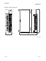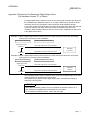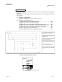
1
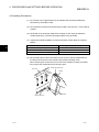
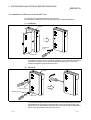
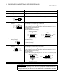
Analog Input/Output Module Type A1S66ADA
,
User s Manual
MODEL
A1S66ADA-U-E
MODEL
CODE
13JL41
Analog Input/Output Module Type A1S66ADA
,
User s Manual
IB(NA)-66819-F(0410)MEE
HEAD OFFICE : 1-8-12, OFFICE TOWER Z 14F HARUMI CHUO-KU 104-6212,JAPAN
NAGOYA WORKS : 1-14 , YADA-MINAMI 5-CHOME , HIGASHI-KU, NAGOYA , JAPAN
When exported from Japan, this manual does not require application to the
Ministry of Economy, Trade and Industry for service transaction permission.
Specifications subject to change without notice.
Mitsubishi Programmable Logic Controller
• SAFETY PRECAUTIONS •
(Always read these instructions before using this equipment.)
Before using this product, please read this manual and the relevant manuals introduced in this manual
carefully and pay full attention to safety to handle the product correctly.
The instructions given in this manual are concerned with this product. For the safety instructions of the
programmable controller system, please read the CPU module user's manual.
In this manual, the safety instructions are ranked as "DANGER" and "CAUTION".
DANGER
Indicates that incorrect handling may cause hazardous conditions,
resulting in death or severe injury.
! CAUTION
Indicates that incorrect handling may cause hazardous conditions,
resulting in medium or slight personal injury or physical damage.
!
Note that the ! CAUTION level may lead to a serious consequence according to the circumstances.
Always follow the instructions of both levels because they are important to personal safety.
Please save this manual to make it accessible when required and always forward it to the end user.
[DESIGN PRECAUTIONS]
!
DANGER
• In case of the external power supply failure or the programmable controller ( PLC ) failure, set up
a safety circuit outside the PLC so that the entire system can operate safely. The mis-output
and malfunction may cause an accident.
!
CAUTION
• Use the PLC in an environment that meets the general specifications contained in this manual.
Using this PLC in an environment outside the range of the general specifications could result in
electric shock, fires, malfunctions, and damage to or deterioration of the product.
• Do not bunch the control wires with the main circuit or power wires, or install them close to each
other. They should be installed 100 mm (3.94 inch) or more from each other. Failure to do so
may result in noise that would cause malfunctions.
• At power ON/OFF, voltage or current may instantaneously be output from the output terminal of
this module.
In such case, wait until the analog output becomes stable to start controlling the external device.
[INSTALLATION PRECAUTIONS]
!
CAUTION
• Insert the tabs at the bottom of the module into the mounting holes in the base unit. If the
module is not properly installed, it may result in malfunctions, failure, or fallout.
• Do not directory touch the module's conductive parts. Doing so could cause malfunctions or
failure in the module.
A-1
A-1
[WIRING PRECAUTIONS]
!
CAUTION
• Ground the AG and FG terminals to the protected grounding conductor when there are a lot of
noise. Failure to ground these terminals may cause malfunctions.
• When wiring PLC, check the rated voltage and terminal layout of the wiring, and make sure the
wiring is done correctly. Connecting a power supply that differs from the rated voltage or wiring
it incorrectly may cause fires or failure.
• Tighten the terminal screws within the range of specified torque.
If the terminal screws are loose, it may result in short circuits or malfunctions.
Tightening the screws too far may cause damage to the screw, resulting in short circuits, or
malfunctions.
• Be sure there are no foreign substances such as sawdust or wiring debris inside the module.
Such debris could cause fires, failure, malfunctions.
[STARTING AND MAINTENANCE PRECAUTIONS]
!
CAUTION
• Do not touch the connector while the power is on. Doing so could cause malfunctions.
• Be sure to shut off all phases of the external power supply used by the system before cleaning
or retightening the terminal screws. If you do not switch off the external power supply, it will
cause failure or malfunctions of the module.
• Do not disassemble or modify the modules. Doing so could cause failure, malfunctions, injury, or
fires.
• Be sure to shut off all phases of the external power supply used by the system before mounting
or dismounting the module. If you do not switch off the external power supply, it will cause failure
or malfunctions of the module.
• Before handling the module, always touch grounded metal, etc. to discharge static electricity
from the human body.
Failure to do so can cause the module to fail or malfunction.
[OPERATING PRECAUTIONS]
!
DANGER
• Do not output (turn ON) the "usage disable" signal as an output signal to special modules from
the PLC CPU.
Outputting the "usage disable" signal may cause PLC system malfunctions.
[DISPOSAL PRECAUTIONS]
!
CAUTION
• When disposing of this product, treat it as industrial waste.
A-2
A-2
REVISIONS
The manual number is given on the bottom left of the back cover.
Print Date
Jan., 1998
Feb., 1998
Manual Number
IB(NA)-66819-A
IB(NA)-66819-B
Revision
First printing
Correction
Section 4.4
Apr., 2001
IB(NA)-66819-C
Addition
WARRANTY
Correction
SAFETY PRECAUTIONS, Chapter2, Section3.1, 3.2, 3.3.3, 3.4.3, 4.2,
4.5.2, 5.3
Mar., 2003
IB(NA)-66819-D
Correction
SAFETY PRECAUTIONS, Section3.1, 3.2, 5.3, Appendix1
July, 2003
IB(NA)-66819-E
Correction
Section5.3
Addition
Appendix3
Oct., 2004
IB(NA)-66819-F
Correction
SAFETY PRECAUTIONS, Section 4.5.2
June, 2005
IB(NA)-66819-G
Addition
Conformation to the EMC Directive and Low Voltage Instruction
Correction
SAFETY PRECAUTIONS, Chapter 5
Japanese Manual Version SH-3642-H
This manual confers no industrial property rights or any rights of any other kind, nor does it confer any patent
licenses. Mitsubishi Electric Corporation cannot be held responsible for any problems involving industrial property
rights which may occur as a result of using the contents noted in this manual.
© 1998 MITSUBISHI ELECTRIC CORPORATION
A-3
A-3
INTRODUCTION
Thank you for purchasing the Mitsubishi Graphic Operation Terminal.
Before using the equipment, please read this manual carefully to develop full familiarity with the functions
and performance of the graphic operation terminal you have purchased, so as to ensure correct use.
Please forward a copy of this manual to the end user.
CONTENTS
1 OVERVIEW
1 - 1 to 1 - 3
1.1 Features ................................................................................................................................................. 1 - 2
1.2 Comparison with A1S63ADA................................................................................................................. 1 - 3
2 SYSTEM CONFIGURATION
2 - 1 to 2- 2
3 SPECIFICATION
3 - 1 to 3 -13
3.1 General Specification............................................................................................................................. 3 - 1
3.2 Performance Specifications ................................................................................................................... 3 - 2
3.3 D/A Conversion I/O Characteristics....................................................................................................... 3 - 4
3.3.1 Voltage output characteristic........................................................................................................... 3 - 5
3.3.2 Current output characteristic........................................................................................................... 3 - 6
3.3.3 Overall accuracy.............................................................................................................................. 3 - 7
3.4 A/D Conversion I/O Characteristic......................................................................................................... 3 - 8
3.4.1 Voltage input characteristic............................................................................................................. 3 - 9
3.4.2 Current input characteristic ............................................................................................................ 3 - 10
3.4.3 Overall accuracy............................................................................................................................. 3 - 11
3.5 I/O Signals Against the PLC CPU ........................................................................................................ 3 - 12
3.5.1 List of I/O signals ............................................................................................................................ 3 - 12
3.5.2 I/O signal functions......................................................................................................................... 3 - 13
4 PROCEDURES AND SETTINGS BEFORE OPERATION
4 - 1 to 4 -12
4.1 Procedures before Operation ................................................................................................................ 4 - 1
4.2 Handling Precautions............................................................................................................................. 4 - 2
4.3 Installation and Removal of the Shield Cover ....................................................................................... 4 - 3
4.4 Part Identification and Settings .............................................................................................................. 4 - 4
4.5 Wiring...................................................................................................................................................... 4 - 7
4.5.1 Precautions when wiring ................................................................................................................. 4 - 7
4.5.2 Wiring between the A1S66ADA and the external devices ............................................................ 4 - 8
4.6 Fine Adjustment of the Offset /Gain Values......................................................................................... 4 - 10
4.6.1 Fine adjustment methods of the offset/gain values....................................................................... 4 - 10
4.7 Maintenance and Inspection................................................................................................................. 4 - 12
A-4
A-4
5 PROGRAMMING
5 - 1 to 5 - 4
5.1 Program Creation Procedures............................................................................................................... 5 5.1.1 Outputting digital values as voltage/current (D/A conversion)....................................................... 5 5.1.2 Receiving voltage/current as digital values (A/D conversion)........................................................ 5 5.2 Basic Read and Write Programs ........................................................................................................... 5 5.3 Program Example .................................................................................................................................. 5 6 TROUBLESHOOTING
APPENDIX
1
1
1
2
3
6 - 1 to 6- 2
App - 1 to App - 5
Appendix 1 Comparison with the Conventional Analog I/O Module (A1S63ADA) ................................App - 1
Appendix 2 External Dimensions.............................................................................................................App - 3
Appendix 3 Precautions For Reading A Digital Output Value (For Hardware Version "C" or Earlier) ...App - 4
A-5
A-5
Conformance to the EMC Directive/Low Voltage Directive
When incorporating the Mitsubishi PLC into other machinery or equipment and keeping compliance with
the EMC and low voltage directives, refer to Chapter 3, "EMC Directives and Low Voltage Directives" of
the User's Manual (Hardware) included with the CPU module or base unit used.
The CE logo is printed on the rating plate on the main body of the PLC that conforms to the EMC directive
and low voltage instruction.
By making this product conform to the EMC directive and low voltage instruction, it is not necessary to
make those steps individually.
A-6
A-6
1 OVERVIEW
MELSEC-A
1 OVERVIEW
1
This user's manual describes the handling, specifications and programing method of
the A1S66ADA type Analog I/O Module (hereafter referred to as A1S66ADA), which is
utilized in combination with the MELSEC-A series CPU module (hereafter referred to
as PLC CPU).The A1S66ADA is a special module with a four-channel analog input
and two-channel analog output.
(Hereinafter, D/A conversion shall mean digital to analog conversion and A/D
conversion shall mean analog to digital conversion.)
(1) D/A conversion
Digital values are converted to analog values such as voltage and current, and
output externally.
(V)
+
100
300
200
-100
400
-300
500
200
Digital values
Analog values
t
0
–
(2) A/D Conversion
Analog values such as voltage and current are converted to digital values so they
can be imported into the PLC CPU.
(V)
+
(V)
+
Analog values
0
–
Digital values
t
0
t
–
The voltage, current and digital values that the A1S66ADA may input or output
are ranged as follows:
Voltage I/O range······0 to 10 V, 1 to 5 V, -10 to 10 V, 0 to 20 mA (switched by
range)
Current I/O range······0 to 20 mA, 4 to 20 mA (switched by range)
Digital output value····0 to 4095 (12 bit binary value)
Digital input value······0 to 4000 (12 bit binary value)
1-1
1-1
1 OVERVIEW
MELSEC-A
1.1 Features
1
(1) High-speed D/A conversion and A/D conversion are possible.
The A1S66ADA can perform conversion at high speeds, as shown below:
240 μs/2 CH or below (for D/A conversion)
400 μs/4 CH or below (for A/D conversion)
(2) High-speed sequence scan is possible
Because the reading and writing of digital and analog values is performed using
I/O signals (X/Y) instead of the buffer memory, which conventionally has been
used, the A1S66DA can reduce the sequence scan time.
Buffer memory method
TO
H0
D0
K5
K1
FROM
H0
K1
D1
K1
Processing time
Item
Command
The digital value
to undergo D/A
conversion is written.
The digital value that
has been undergone
A/D conversion is read.
A2USHCPU
Q2ASHCPU
TO
212.1 μs
162.0 μs
FROM
183.5 μs
160.0 μs
395.6 μs
322.0 μs
Total
I/O signal (X/Y) format
MOV
(D/A conversion)
MOV
(A/D conversion)
Total
D0
K3Y0
MOV
K3X0
D100
The digital value
to undergo D/A
conversion is written.
The digital value that
has been undergone
A/D conversion is read.
Processing time
Item
Command
MOV
A2USHCPU
Q2ASHCPU
0.55 μs
0.30 μs
0.55 μs
0.30 μs
1.10 μs
0.60 μs
(3) D/A conversion and A/D conversion may be performed with one
module.
An A1S66ADA module can perform D/A conversion at two channels and A/D
conversion at four channels.
1-2
1-2
1 OVERVIEW
MELSEC-A
1.2 Comparison with A1S63ADA
The following is a comparison with the conventional analog I/O module (A1S63ADA).
1. Number of channels
A1S66ADA
A1S63ADA
Number of
Type
Output
2 channels
1 channel
channels
Input
4 channels
2 channels
Type
A1S66ADA
A1S63ADA
D/A
conversion
Conversion speed
A/D
conversion
240 µs/2 channels or below
(Resolution 1/4000)
400 µs/4 channels or below
(Resolution 1/4000)
2. Maximum conversion speed
1 µs/CH (Resolution 1/4000)
2 µs/CH (Resolution 1/8000)
3 µs/CH (Resolution 1/12000)
3. D/A conversion
Type
A1S66ADA
Voltage output
Current output
Digital input
0 to 4000 (12 - bit binary value)
Analog output
Voltage: -10 to 10 V DC
(External load resistance 2 kΩ to 1 MΩ)
Current: 0 to 20 mA DC
(External load resistance 0 Ω to 600 Ω)
A1S63ADA
Voltage output
Current output
0 to 4000
-4000 to 4000
(Resolution 1/4000)
(Resolution 1/4000)
0 to 8000
-8000 to 8000
(Resolution 1/8000)
(Resolution 1/8000)
0 to 12000
-12000 to 12000
(Resolution 1/12000)
(Resolution 1/12000)
Voltage: -10 to 0 to 10 V DC
(External load resistance 2 kΩ to 1 MΩ)
Current: -20 to 20 mA DC
(External load resistance 0 Ω to 600 Ω)
4. A/D conversion
Type
A1S66ADA
A1S63ADA
Analog input
Voltage: -10 to 0 to 10 V DC
(Input resistance 1 MΩ)
Current: 0 to 20 mA DC
(Input resistance 250 Ω)
Voltage: -10 to 0 to 10 V DC (Input resistance 1 MΩ)
Current: -20 to 20 mA DC (Input resistance 250 Ω)
Digital output
0 to 4095 (12 - bit binary value)
-4096 to 4095 (Resolution 1/4000)
-8192 to 8191 (Resolution 1/8000)
-12288 to 12287 (Resolution 1/12000)
5. Accuracy
Type
Accuracy
1-3
A1S66ADA
A1S63ADA
Within ± 1 %
1-3
2 SYSTEM CONFIGURATION
MELSEC-A
2 SYSTEM CONFIGURATION
(1) Applicable CPU
· A1SCPU(S1)
· A1SJCPU(S3)
· A2ASCPU(S1/S30) · A2SCPU(S1)
· A1SJHCPU(S8) · A1SHCPU
· A2SHCPU(S1)
· A2USHCPU-S1
· Q2ASCPU(S1) · Q2ASHCPU(S1) · A1SCPU24-R2
2
· A52GCPU(T21B)
(2) Number of modules loaded
As long as the number of I/O points for the applicable CPU is not exceeded,
there is no limit in the number of modules used.
(3) Slots for loading
The module may be loaded into any of the base module slots, expect the
following:
If the module is loaded in a slot on an extension base module that is not
equipped with a power supply module (A1S52B, A1S55B or A1S58B), the power
capacity may be insufficient to cover all the modules.
When loading to an A1S66ADA extension base module without a power supply
module, select a proper power supply module, basic base module, extension
base module and extension cable by taking the following points into
consideration:
1) Current capacity of the power supply module on the basic base module
2) Voltage drops of the basic base module
3) Voltage drops of the extension base module
4) Voltage drops in the extension cable
(4) Data link system
In a data link system, the module may be loaded to the master station, local
station or remote I/O station. Refer to the MELSECNET or MELSECNET/B Data
Link System Reference Manual for program examples for remote I/O stations.
Remark
Refer to the respective manual listed below for calculation methods for the range of
I/O points and voltage drops. This shows the system configuration when using the
graphics software to create monitor screens.
• A1SJCPU(S3) User's Manual·····························································IB(NA)-66446
• A1S/A1SC24-R2/A2SCPU(S1) User's Manual··································IB(NA)-66320
• A2ASCPU(S1/S30) User's Manual·····················································IB(NA)-66455
• A2USHCPU-S1 User's Manual···························································IB(NA)-66789
• A1SJH(S8)/A1SH/A2SHCPU(S1) User's Manual······························IB(NA)-66779
• Q2AS(H)CPU(S1) User's Manual·······················································SH(NA)-3599
2-1
2-1
2 SYSTEM CONFIGURATION
MELSEC-A
MEMO
2
2-2
2-2
3 SPECIFICATION
MELSEC-A
3 SPECIFICATION
This section explains the A1S66ADA the general specifications, performance
specifications and I/O signals.
3.1 General Specification
This section explains the A1SJ71PB92D general specifications.
Table 3.1 General specification
3
Item
Specifications
Operating ambient
0 to 55 °C
temperature
Storage ambient
-20 to 75 °C
temperature
Operating ambient
10 to 90 % RH, No condensation
humidity
Storage ambient
10 to 90 % RH, No condensation
humidity
Frequency
Conforming
Vibration
to JIS B
resistance
3502, IEC
61131-2
When there is
intermittent
vibration
When there is
continuous
vibration
Shock resistance
Acceleration
10 to 57 Hz
—
(0.003 in.)
2
57 to 150 Hz
9.8 m/s
10 to 57 Hz
—
57 to 150 Hz
Sweep Count
—
10 times
each in X, Y
0.035 mm
and Z axis
(0.001 in.)
(80 minutes)
2
4.9 m/s
—
2
Conforming to JIS B3502, IEC 61131-2 (147 m/s , 3 times each in 3 directions)
Operating
No corrosive gas present
environment
Operating height
2000 m(6562 ft) or less
Installation area
On the control board
Over-voltage
category 1
Pollution rate
Amplitude
0.075 mm
II or less
2
2 or less
1: Indicates the distribution area where the device is assumed to be connected, from the public power distribution network
to the local machine device.
Category II is applied to the devices to which the power is supplied from a fixed equipment.
The surge resistance voltage of a rated 300 V device is 2500 V.
2: This is an index which indicates the occurrence rate of the conductive object in the environment where the device is
used.
Pollution rate II indicates that only non-conductive pollution may occur with a possibility of generating temporary
conductivity due to accidental condensation.
3: Do not use or store the PLC under pressure higher than the atmospheric pressure of altitude 0m.
Doing so can cause a malfunction.
When using the PLC under pressure, please contact your sales representative.
3-1
3-1
3 SPECIFICATION
MELSEC-A
3.2 Performance Specifications
The Table 3.2 describes the performance specifications of the A1S66ADA.
Table 3.2 Performance specification of the A1S66ADA
Item
Performance specifications
—
Voltage output
Digital input
Current output
0 to 4000 (12-bit binary value)
-10 to 10 V DC
(External load resistance : 2 kΩ to 1 MΩ)
Analog output
0 to 20 mA DC
(External load resistance : 0 Ω to 600 Ω)
Analog output
I/O characteristics
1
D/A conversion
0 to 10 V
range
0 to 5 V
range
1 to 5 V
range
-10 to 10 V
range
Digital input
0 to 20 mA
range
4 to 20 mA
range
0
1000
2000
3000
4000
0V
2.5 V
5V
7.5 V
10 V
0V
1.25 V
2.5 V
3.75 V
5V
1V
2V
3V
4V
5V
-10 V
-5 V
0V
5V
10 V
0
1000
2000
3000
4000
0 mA
5 mA
10 mA
15 mA
20 mA
4 mA
8 mA
12 mA
16 mA
20 mA
1.25 mV
1.0 mV
5.0 mV
5 μA
4 μA
Maximum resolution
Conversion speed
2.5 mV
2
240 μs/2 channels or less (Sampling : 80 μs/1 channel)
Absolute maximum
output
Output short protection
Voltage : ±12 V
2 channels
Adjust the two channels simultaneously with the control knob on the front side of the module.
The adjustment should be done on-line.
Offset/gain adjustment
Voltage : -10 to 0 to 10 V DC (Input resistance: 1 MΩ)
Current: 0 to 20 mA DC (Input resistance: 250 Ω)
Analog input
Digital output
Analog input (voltage)
0 to 10 V
range
3
D/A conversion
Maximum resolution
Conversion speed
4
Absolute maximum
input
Analog input points
Offset/gain adjustment
3-2
Current : +28 mA
Present
Analog output points
I/O characteristics
Analog output
Digital input
0 to 4095 (12-bit binary value)
Analog input (current)
-10 to10 V
range
0 to 20 mA
range
4 to 20 mA
range
Digital output
1V
2V
3V
4V
5V
-10 V
-5 V
0V
5V
10 V
0 mA
5 mA
10 mA
15 mA
20 mA
4 mA
8 mA
12 mA
16 mA
20 mA
0
1000
2000
3000
4000
1.0 mV
5.0 mV
5 μA
4 μA
0 to 5 V range 1 to 5 V range
0V
2.5 V
5V
7.5 V
10 V
0V
1.25 V
2.5 V
3.75 V
5V
2.5 mV
1.25 mV
400 μs/4 channels or less (Sampling : 80 μs/1 channel)
Voltage : ±15 V
Current : ±30 mA
4 channels
Adjust the four channels simultaneously with the control knob on the front side of the module.
Check the digital output value on-line while making the adjustments.
3-2
3
3 SPECIFICATION
MELSEC-A
Table 3.2 Performance specification of the A1S66ADA (continued)
Item
Overall
accuracy
Performance specifications
D/A conversion
(accuracy against the
maximum value)
A/D conversion
(accuracy against the
scale)
current output
Within ±1% (±100 mV)
Within ±1% (±200 µA)
Within ±1% (±40)
Between I/O terminals and PLC power supply········Photocoupler isolation
Between each channel········No isolation
Insulation method
64 points (Input 64 points, output 64 points)
Number of occupying I/O points
Connecting terminal base
20-point terminal base (M3.5
0.75 to 1.25 mm
Applicable wire size
5
7 screws)
2
R1.25 - 3 1.25 - YS3 2 - 3.5 2 - YS3A
V1.25 - M3 V1.25 -YS3A V2 - S3 V2 - YS3A
Applicable solderless terminal
5 V DC internal current consumption
External power
supply
Voltage output
Voltage
0.21 A
21.6 to 26.4 V DC
Current
consumption
0.16 A
Weight
0.33 kg
1 The analog output range is set commonly for CH1 to CH2.
2 The conversion speed refers to the speed between the times when a digital value is written to the
A1S66ADA and when an analog output which corresponds to the aforementioned value begins to be
outputted.
3 The analog input range is set commonly for CH3 to CH6.
4 The conversion speed refers to the speed while a change in an analog input is converted to a digital
output. (Excluding the sequence scan)
5 Inputs and outputs are assigned to the same number. Therefore, the I/O occupied points are 64.
POINT
When utilizing the peripheral device to assign the I/O numbers, set it as a 64-point
output module.
3-3
3-3
3 SPECIFICATION
MELSEC-A
3.3 D/A Conversion I/O Characteristics
The I/O characteristic of D/A conversion will be explained below.
(1) I/O conversion characteristic
The I/O conversion characteristic refers to the angle produced by a straight line
connecting the "offset value" and "gain value" created when the digital values set
by the PLC CPU are converted to analog values (voltage or current).
(2) Offset value and gain value
Offset value and gain value are defined as follows:
(a) Offset value···The current value or voltage value that is output from the A1S66ADA
when the digital value set by the PLC CPU is "0."
(b) Gain value·····The current value or voltage value that is output from the A1S66ADA
when the digital value set by the PLC CPU is "4000."
(3) I/O conversion characteristic
Examples of A1S66ADA's I/O conversion characteristic are shown below.
When the offset value is -10V and gain value is 10V
(V)
Analog output voltage
10
5
Gain value
0
-5
-10
0
2000
4000
Digital input value
Offset value
Voltage output characteristic
When the offset value is 0 mA and gain value is 20 mA
(mA)
Analog output current
10
5
Gain value
0
-5
-10
0
Offset value
2000
4000
Digital input value
Current output characteristic
3-4
3-4
3 SPECIFICATION
MELSEC-A
3.3.1 Voltage output characteristic
An example of voltage output characteristic graph when the offset and gain settings
are changed is shown in Fig. 3.1.
(V)
Analog output voltage
10
1)
5
3)
The I/O conversion characteristic when the off set
value and gain value are set, as shown in the
table below, is shown in the figure at left.
2)
0
Offset value
Gain value
1)
0V
10 V
2)
0V
5V
3)
1V
5V
4)
-10 V
10 V
4)
-5
-10
2000
Digital input value
0
4000
Fig. 3.1 Voltage output characteristic graph
[Example]
On the characteristic graphs 1) to 4), the analog output voltage will be as follows when
the digital input value is set to 500 and 2000:
No.
1)
2)
3)
4)
3-5
Digital input value
Analog output value
500
1.25 V
2000
5V
500
0.625 V
2000
2.5 V
500
1.5 V
2000
3V
500
-7.5 V
2000
0V
3-5
3 SPECIFICATION
MELSEC-A
3.3.2 Current output characteristic
An example of current output characteristic graph when the offset and gain settings are
changed is shown in Fig. 3.2.
(m A)
Analog output current
20
15
2)
10
The I/O conversion characteristic when the off set
value and gain value are set, as shown in the
table below, is shown in the figure at left.
1)
5
Offset value
Gain value
1)
0 mA
20 mA
2)
4 mA
20 mA
0
4000
2000
0
Digital input value
Fig. 3.2 Current output characteristic graph
[Example]
On the characteristic graphs 1) to 2), the analog output voltage will be as follows when
the digital input value is set to 1000 and 2000:
No.
1)
2)
3-6
Digital input value
Analog output value
1000
5 mA
2000
10 mA
1000
8 mA
2000
12 mA
3-6
3 SPECIFICATION
MELSEC-A
3.3.3 Overall accuracy
Overall accuracy refers to the accuracy relative to the maximum analog output value.
Even if the output characteristic is altered by changing the offset/gain settings, the
overall accuracy does not change but is maintained within the performance range as
outlined in the specifications.
The overall accuracy of voltage and current output characteristics are shown in Fig. 3.3
and 3.4.
The overall accuracy of the voltage output
is the accuracy against 10V.
Analog output value
+10V
Fluctuation will be within 10 V
±1% (100 mV) width due to
the operating environment
(ambient temperature, noise).
0V
-10V
0
2000
Digital input value
4000
Fig. 3.3 Overall accuracy of voltage output characteristics
The overall accuracy of the current output
is the accuracy against 20 mA.
20mA
Analog output value
Fluctuation will be within 20 mA
±1% (200 µA) width due to
the operating environment
(ambient temperature, noise).
0mA
0
Digital input value
4000
Fig. 3.4 Overall accuracy of current output characteristic
3-7
3-7
3 SPECIFICATION
MELSEC-A
3.4 A/D Conversion I/O Characteristic
The I/O characteristic of A/D conversion will be explained below.
(1) I/O conversion characteristic
The I/O conversion characteristic refers to the angle produced when the "offset
value" and "gain value" created when the analog values (voltage or current) from
outside the PLC are converted to digital values are connected with a straight line.
The I/O conversion characteristic refers to the angle produced by a straight line
that connects the "offset value" and "gain value" created when the digital values
set by the PLC CPU are converted to analog values (voltage or current).
(2) Offset value and gain value
Offset value and gain value are defined as follows:
(a) Offset value····The analog value (voltage or current) that makes the digital output
value "0."
(b) Gain value······The analog value (voltage or current) that makes the digital output
value "4000."
(3) I/O conversion characteristic
Examples of A1S66ADA's I/O conversion characteristic are shown below.
When the offset value is -10 V and gain value is 10 V
Digital output value
4000
3000
Gain value
2000
1000
0
-10
Offset value
0
Analog input voltage (V)
10
Voltage input characteristic
When the offset value is 0 mA and gain value is 20 mA
Digital output value
4000
3000
Gain value
2000
1000
0
0
10
Analog input current (mA)
20
Offset value
Current input characteristic
3-8
3-8
3 SPECIFICATION
MELSEC-A
3.4.1 Voltage input characteristic
An example of voltage input characteristic graph when the offset/gain settings are
changed is shown in Fig. 3.5.
Digital output vallue
4000
3000
The voltage input characteristic when the
offset value and gain value are set as shown
in the table below, is shown in the figure.
3)
2000
2)
1)
Offset value
Gain value
1)
0V
10 V
2)
0V
5V
3)
1V
5V
4)
-10 V
10 V
4)
1000
0
10
0
-10
Analog input voltage (V)
Fig. 3.5 Voltage input characteristic graph
[Example]
On the characteristic graphs 1) to 4), the digital output voltage will be as follows when
the analog input value is set to 1 V and 3 V:
No.
Analog input value
Digital output value
1V
400
3V
1200
1V
800
3V
2400
1)
2)
3)
4)
1V
0
3V
2000
1V
2200
3V
2600
POINT
• When a voltage that exceeds the range of -15 V to 15 V is input, the elements
may be damaged.
• The overall accuracy is the accuracy outlined in the performance specifications
when the input voltage is in the range of -10 to 10 V. If the input voltage is
outside the range of -10 to 10 V, the accuracy may not be as indicated in the
performance specifications.
• When a value which causes the digital output value to exceed the maximum
(4095) or minimum (0) digital value is input, the digital output value will be fixed at
the maximum (4095) or minimum (0) digital value.
3-9
3-9
3 SPECIFICATION
MELSEC-A
3.4.2 Current input characteristic
An example of current input characteristic graph when the offset/gain settings are
changed is shown in Fig. 3.6.
(V)
Digital output vallue
4000
3000
The current input characteristic when the
offset value and gain value are set as shown
in the table below is shown in the figure at
left.
2000
1)
1000
2)
0
10
Analog input current (m A)
0
20
Offset value
Gain value
1)
0 mA
20 mA
2)
4 mA
20 mA
Fig. 3.6 Current input characteristic graph
[Example]
On the characteristic graphs 1) to 2), the digital output current will be as follows when
the analog input value is set to 5 mA and 12 mA:
No.
Analog input value
Digital output value
1)
2)
5 mA
1000
12 mA
2400
8 mA
250
12 mA
2000
POINT
• When a current exceeding the range of -30mA to 30mA is input, the elements
may be damaged due to heating.
• The overall accuracy is the accuracy outlined in the performance specifications
when the input current is in the range of 0 to 20mA. If the input current is outside
the range of 0 to 20mA, the accuracy may not be as indicated in the performance
specifications.
• When a value which causes the digital output value to exceed the maximum
(4000) or minimum (0) digital value is input, the digital output value will be fixed at
the maximum (4000) or minimum (0) digital value.
3 - 10
3 - 10
3 SPECIFICATION
MELSEC-A
3.4.3 Overall accuracy
The overall accuracy refers to the accuracy relative to the maximum digital output
value.
Even if the I/O characteristic is altered by changing the offset/gain settings, the overall
accuracy does not change but is maintained within the performance range as outlined
in the specification. The overall accuracy of voltage and current input characteristics
are shown in Fig. 3.7 and 3.8.
Offset value -- 0 V, gain value -- 10 V, resolution -- 1/4000
4000
Digital output value
3000
±1 % (±40)
2000
-5
5
1000
0-15
-10
0
Analog input voltage (V)
15
10
Fig. 3.7 Overall accuracy of voltage input characteristic
4095
Offset value -- 0 mA, gain value -- 20 mA, resolution -- 1/4000
4000
Digital output value
±1 % (±40)
2000
0
0
10
Analog input current (mA)
20
Fig. 3.8 Overall accuracy of current input characteristic
3 - 11
3 - 11
3 SPECIFICATION
MELSEC-A
3.5 I/O Signals Against the PLC CPU
3.5.1 List of I/O signals
The A1S66ADA utilizes 64 input points and 64 output points for the communication
with the PLC CPU.
The device numbers of the I/O signals and signal names are shown in Table 3.3.
The device X indicates the input signal from the A1S66ADA to the PLC CPU, and the
device Y the output signal from the PLC CPU to the A1S66ADA.
The I/O numbers indicated the occasion when the A1S66ADA is installed in the "slot 0"
of the basic base.
Table 3.3 List of the A1S66ADA I/O signals
Signal Direction A1S66ADA
PLC CPU
Signal Direction PLC CPU
A1S66ADA
Device No.
Signal Name
Device No.
Signal Name
X00 to X0B
CH3 digital output value
Y00 to Y0B
CH1 digital value setting
X0C to X0F
Usage disable
Y0C to Y0E
X10 to X1B
CH4 digital output value
X1C to X1F
Usage disable
X20 to X2B
CH5 digital output value
X2C to X2F
Usage disable
X30 to X3B
CH6 digital output value
X3C to X3F
Usage disable
Y0F
Usage disable
CH1 D/A conversion value output
enable flag
Y10 to Y1B
CH2 digital value setting
Y1C to Y1E
Usage disable
Y1F
Y20 to Y3F
CH2 D/A conversion value output
enable flag
Usage disable
POINT
• Do not output (turn ON) the "usage disable" signal as an output signal to special
modules from the PLC CPU. Outputting the "usage disable" signal may cause
PLC system malfunctions.
3 - 12
3 - 12
3 SPECIFICATION
MELSEC-A
3.5.2 I/O signal functions
I/O signal functions of the A1S66ADA are explained below.
(1) X00 to X0B, X10 to X1B, X20 to X2B, X30 to X3B: Digital output
value
The A/D converted digital values in CH3 to CH6 are stored in Xn0 to XnB as
binary data, as shown below:
XnB
XnA
Xn9
Xn8
Xn7
Xn6
Xn5
Xn4
Xn3
Xn2
Xn1
Xn0
b11
b10
b9
b8
b7
b6
b5
b4
b3
b2
b1
b0
Xn0
Digital output value (0 to 4095)
(Example) When the digital output value in CH3 is 2000 (H07D0)
XnB
0
XnA
Xn9
1
1
Xn8
Xn7
Xn6
Xn5
Xn4
Xn3
Xn2
Xn1
1
1
1
0
1
0
0
0
7
D
0
0
(2) Y00 to Y0B, Y10 Y1B: Digital value setting
The digital values to be D/A converted in CH1 and CH2 are set in Yn0 to YnB as
binary data, as shown below:
YnB
YnA
Yn9
Yn8
Yn7
Yn6
Yn5
Yn4
Yn3
Yn2
Yn1
Yn0
b11
b10
b9
b8
b7
b6
b5
b4
b3
b2
b1
b0
Digital value setting (0 to 4000)
(Example) When the digital value in CH2 is set to 2500 (H09C4)
YnB
YnA
Yn9
Yn8
Yn7
1
0
0
1
1
9
Yn6
Yn5
Yn4
Yn3
Yn2
Yn1
Yn0
1
0
0
0
1
0
0
C
4
(3) Y0F, Y1F: CH1, CH2 D/A conversion value output enable flag
Outputting the D/A converted analog value to outside the module may be
enabled or disabled.
ON·······Output enabled
The D/A converted analog value is output externally.
OFF·····Output disabled
The analog value 0 V/0 mA is output.
3 - 13
3 - 13
4 PROCEDURES AND SETTINGS BEFORE OPERATION
MELSEC-A
4 PROCEDURES AND SETTINGS BEFORE OPERATION
The procedures before operation, handling precautions, name and setting for each
area, wiring, etc. will be explained below.
4.1 Procedures before Operation
The procedures before the operation of the module are shown in Fig. 4.1 below.
Start
Module installation
• Install the A1S66ADA in the appropriate slot.
Wiring
4
Refer to Section 4.5
• Perform wiring for A1S66ADA and external
devices.
Offset/Gain Settings
• Set the offset values and gain values for the
channels to be used.
Programming, Debugging
Refer to Section 4.6
Refer to Chapter 5
• Create and check programs for reading and
writing to the A1SA66ADA from the PC CPU.
End
Fig. 4.1 Procedures before operation
4-1
4-1
4 PROCEDURES AND SETTINGS BEFORE OPERATION
MELSEC-A
4.2 Handling Precautions
(1) Do not drop or put a great impact on the module case and the terminal block
because they are made of resin.
(2) Do not take the printed circuit board of the module out of the case. It may result in
a failure.
(3) Be careful not to let foreign matter such as filings or wire chips get inside the
module while wiring. Remove all foreign matters if any get inside.
(4) Tighten the module installation screws and terminal screws within the range as
follows :
4
Screw Area
Tightening Torque Range
Module fixing screws (M4 screw)
78 to 118 N·cm
Terminal block terminal screws (M3.5 screw)
59 to 88 N·cm
Terminal block installation screws (M4 screw)
78 to 118 N·cm
(5) When loading the module to the base unit, be sure to insert the module latch to
the fixing hole, and secure the module using module mounting screw.
When removing the module, be sure to remove the module mounting screw first,
then remove the module latch from the fixing hole.
Module mounting screw
Base unit
Module
connector
Module fixing hole
4-2
Module
Module latch
4-2
4 PROCEDURES AND SETTINGS BEFORE OPERATION
MELSEC-A
4.3 Installation and Removal of the Shield Cover
It is necessary to install the shield cover when using.
Procedures for installing and removing the shield cover are described below.
(1) Installation
Module
Shield fixing
screw
Shield cover
To install the shield cover to the module, install the cover to the terminal side first
as shown in the figure, then it will be completed by pushing the cover to the
module and tightening the shield fixing screw.
(2) Removal
Module
Hole for removal
Shield fixing screw
Shield cover
To remove the shield cover from the module, remove the shield fixing screw first
and install the tip of a flat-tip screwdriver into the removal hole as shown in the
figure, then move the screwdriver towards the rear of the module to separate the
clip from the removal hole and remove the cover.
4-3
4-3
4 PROCEDURES AND SETTINGS BEFORE OPERATION
MELSEC-A
4.4 Part Identification and Settings
The following describes the part names and settings of the A1S66ADA :
11)
1)
A1S66ADA
D/A
A/D
2)
RUN
D/A
OFFSET
4)
3)
13)
A/D
GAIN
6)
V+
COM
C
H
1
I+
O
U
T
C
H
2
7)
8)
9)
10)
C
H
3
I
N
C
H
4
C
H
5
I
N
C
H
6
1
2
4
I+
V+ I+
6
V– I–
SLD
V+ I+
V– I–
V+ I+
V– I–
SLD
V+ I+
V– I–
AG
(FG)
INPUT
24VDC
12)
CH3
CH4
CH5
CH6
V I
3
V+
COM
D/A A/D
0~±10 V
0~20 mA
A1S66ADA
4-4
5)
0-10V
0-5V
1-5V
10-10V
5
7
8
9
14)
10
11
12
13
14
15
16
17
18
19
20
4-4
4 PROCEDURES AND SETTINGS BEFORE OPERATION
No.
1)
Name
RUN LED
RUN
2)
D/A conversion offset control knob
D/A
OFFSET
3)
D/A conversion gain control knob
D/A
GAIN
4)
A/D conversion offset control knob
A/D
OFFSET
5)
A/D conversion gain control knob
A/D
GAIN
6)
O
U
T
C
H
2
Indicates the operating conditions of the A1S66ADA
On : Power is ON
Off : Power is OFF
Used when making a fine adjustment of the D/A conversion offset.
The offset value is increased by turning the control knob to the right.
The offset value is decreased by turning the control knob to the left.
Used when making a fine adjustment of the D/A conversion gain.
The gain value is increased by turning the control knob to the right.
The gain value is decreased by turning the control knob to the left.
Used when making a fine adjustment of the A/D conversion offset.
The offset value is increased by turning the control knob to the right.
The offset value is decreased by turning the control knob to the left.
Used when making a fine adjustment of the A/D conversion gain.
The gain value is increased by turning the control knob to the right.
The gain value is decreased by turning the control knob to the left.
V+
COM
I+
V+
COM
I+
Analog input terminal
(CH3 to CH6)
C
H
3
I
N
C
H
4
C
H
5
I
N
C
H
6
4-5
Description
Analog output terminal (CH1, CH2) Outputs the analog values (voltage/current) of CH1 to CH2.
Refer to Section 4.5.2 on the wiring method.
C
H
1
7)
MELSEC-A
Inputs the analog values (voltage/current) of CH3 to CH6.
Refer to Section 4.5.2 on the wiring method.
V+ I+
V– I–
SLD
V+ I+
V– I–
V+ I+
V– I–
SLD
V+ I+
V– I–
4-5
4 PROCEDURES AND SETTINGS BEFORE OPERATION
No.
Name
MELSEC-A
Description
8)
Analog ground terminal
The ground terminal of the analog signal
(Refer to Section 4.4 on the wiring method.)
9)
Frame ground terminal
The ground terminal of the shielded cable
(Refer to Section 4.4 on the wiring method.)
10)
Power supply input terminal
Connect 24 V DC at the input terminal of the power supply.
INPUT
24 V DC
D/A A/D
0 to ±10 V
0 to 20 mA
11)
Analog-output range switching
setting pin
D/A
0 ~ 10 V
0~5V
1~5V
-10 ~ 10 V
Set the analog output range. CH1, CH2 common.
When setting the current output range, set as follows:
When switching to 0 to 20 mA
Set a jumper at a position between 0 V and 5 V.
When switching to 4 to 20 mA
Set a jumper at a position between 1 V and 5 V.
Set the jumper as it always makes a line.
(Set it with the jumper)
(Setting at shipment : 0 to 10 V range )
(Example) When the analog output range is set to 0 to 10 V or 0 to 20 mA, the jumper
should be set as follows.
D/A
D/A
Jumper
0 ~ 10 V
0~5V
1~5V
-10 ~ 10 V
0 ~ 10 V
0~5V
1~5V
-10 ~ 10 V
When setting to 0 to 10 V
12)
Analog-input voltage/current
switching setting pin
CH3
CH4
CH5
CH6
Jumper
When setting to 0 to 20 mA
Set the analog input (voltage input or current input ) for each channel (CH3 to CH6).
(Set it with the jumper)
(Setting at shipment : V)
For voltage input setting : V
For current input setting : I
V I
13)
Analog-input range switching
setting pin
A/D
0 ~ 10 V
0~5V
1~5V
-10 ~ 10 V
Set the analog input range. CH3 to CH6 common.
When setting the current input range, set as follows:
When switching to 0 to 20 mA
Set a jumper at a position between 0 V and 5 V.
When switching to 4 to 20 mA
Set a jumper at a position between 1 V and 5 V.
(Setting at shipment : 0 to 10 V range )
(Set it with the jumper)
(Example) When the analog input range is set to -10 to 10 V or 4 to 20 mA, the jumper
should be set as follows.
0 ~ 10V
0 ~ 5V
1 ~ 5V
-10 ~ 10V
A/D
Jumper
A/D
0 ~ 10V
0 ~ 5V
1 ~ 5V
-10 ~ 10V
When setting to 4 to 20 mA
Jumper
When setting to -10 to 10 V
14)
Terminal block
Numbers in a diagram indicates terminal numbers.
IMPORTANT
When inputting or outputting current, do not set a jumper at a position between 0 V
and 10V or between -10 V and 10 V of the analog-input and output range switching
setting pin. This may cause a module breakdown or malfunction.
4-6
4-6
4 PROCEDURES AND SETTINGS BEFORE OPERATION
MELSEC-A
4.5 Wiring
The following describes the precautionary items on wiring as well as wiring to the
external devices.
4.5.1 Precautions when wiring
To obtain the maximum performance from the functions of A1S66ADA and improve
the system reliability, a wiring with the high durability against the noise is required. The
external wiring precautions described below make more improvement in the wiring not
to be affected by the noise.
(1) Use separate cables for the AC and the analog input to the A1S66ADA, in order
not to be affected by the AC side surge or conductivity.
(2) Do not bundle or place the cable close to the main circuit line, high voltage line or
load carrying wires from other than the PLC. It is influenced more easily by the
noise, surge, or conductivity.
(3) Place a one-point grounding on the PLC side for the shield line or shield cable.
However, depending on the external noise conditions, it may be better to have a
grounding externally.
4-7
4-7
4 PROCEDURES AND SETTINGS BEFORE OPERATION
MELSEC-A
4.5.2 Wiring between the A1S66ADA and the external devices
The following shows the wiring method for the A1S66ADA.
(1) CH1 and CH2
(a) For voltage output
1
2
CH1 or CH2
D/A
conversion
circuit
Motor drive
module, etc.
2k
V+
COM
to
1M
GND
(b) For current output
1
2
Motor drive
module, etc.
CH1 or CH2
D/A
conversion
circuit
I+
COM
0
to
600
GND
1 Use a two-core twisted shield line for the power cable.
2 When noise or ripple occurs with the external cable, connect a condenser
with 0.1 to 0.47 µ FWV to the input terminal of the external device.
IMPORTANT
The voltage and current output can not be used simultaneously on the same
channel.
In the event it is used, the internal elements are destroyed; therefore always open
unused terminals.
4-8
4-8
4 PROCEDURES AND SETTINGS BEFORE OPERATION
MELSEC-A
(2) CH3 to CH6
(a) For voltage input
*3
+15V
Signal source
0 to
CH3
10
500k
V+I+
V-ISLD
500k
*1 Shield
-15V
*2
(b) For current input
Signal source
0 to
CH6
10
V+I+
V-ISLD
FG
500k
250k
500k
FG
*5
*6
Power supply module
GND
AG
*4
1 Use a two-core twisted shield line for the power cable.
2 Indicates the A1S66ADA input resistance.
3 When noise or ripple occurs with the external cable, connect a condenser
with about 0.1 to 0.47 µ F(Part with voltage resistance of 25V or more)
between the terminal V+I+ and V-I-.
4 The FG terminal of the power supply module should always be grounded.
5 Make sure to connect between the FG of the power supply module and the
FG of A1S66ADA.
6 Due to noise in the environment, AG terminal may attain better accuracy
when grounded.
POINT
The FG terminal of A1S66ADA and the FG terminal of the power supply module
are not connected.
4-9
4-9
4 PROCEDURES AND SETTINGS BEFORE OPERATION
MELSEC-A
4.6 Fine Adjustment of the Offset /Gain Values
Offset/gain values are set by selecting an I/O characteristic, which is preset using the
analog input/output range switch setting pins.
Each module will have slight characteristic differences from the I/O characteristic
selected by the analog input/output range switch setting pins due to the ambient
temperature, characteristic variances of the A/D conversion module, and so on.
Offset/gain fine adjustment is performed to correct such slight differences in
characteristics.
4.6.1 Fine adjustment methods of the offset/gain values
The following flow chart describes the fine adjustment procedure of the offset/gain
value of A1s66ADA. This setting is for when the module is installed in the slot No. 0,
the D/A conversion to CH1 and A/D conversion to CH3.
(1) Fine adjustment procedures for the D/A conversion offset/gain
values
Start
Set the analog output range by using
the analog-output range switching setting pin.
Input the offset value to the
output signals Y00 to Y0B.
Fine adjustment of
the offset value.
Turn on the CH1 D/A conversion
value output enable flag (Y0F).
Adjust the analog output of the CH1 that
corresponds to the offset value using
"D/A conversion offset control knob".
Input the gain value to the
output signals Y00 to Y0B.
Fine adjustment of
the gain value.
Adjust the analog output of the CH1 that corresponds to
the gain value using "D/A conversion gain control knob".
End
POINT
If the analog output range is set to -10 V to 10 V, and if a fine adjustment of the
offset value is performed by setting the offset value to 0 and the analog output to 10 V, the analog output may shift slightly. In such cases, the offset value can be
set correctly in one attempt if fine adjustment of the offset value is performed by
setting the offset value to 2000 and the analog output to 0 V.
4 - 10
4 - 10
4 PROCEDURES AND SETTINGS BEFORE OPERATION
MELSEC-A
(2) Fine adjustment procedure for the A/D conversion offset/gain
values
Start
Select the analog input (voltage/current input )
with the analog-input voltage/current switching
setting pin.
Set the input range by using the analoginput range switching setting pin.
Monitor the binary value by the input signals X00
to X0B as 1 word data.
Fine adjustment of
the offset value.
Input to CH3 the voltage/current
that corresponds to the offset value.
Adjust the CH3 digital output value (X00 to X0B)
using "A/D conversion offset control knob" so
that the value is the same as the offset value.
Input the voltage/current that
corresponds to the gain to CH3.
Fine adjustment of
the gain value.
Adjust the CH3 digital output value (X00 to X0B)
using "A/D conversion gain control knob" so
that the value is the same as the gain value.
End
POINT
Disconnect the power supply for the PLC CPU or the external power supply for
A1S66ADA at all phases when setting the output range and making voltage/current
selection.
4 - 11
4 - 11
4 PROCEDURES AND SETTINGS BEFORE OPERATION
MELSEC-A
4.7 Maintenance and Inspection
The A1S66ADA has no particular inspection items, but in order to maintain the system
in the best condition, perform inspection according to the categories listed in the PLC
CPU Users' Manual.
4 - 12
4 - 12
5 PROGRAMMING
MELSEC-A
5 PROGRAMMING
The program creation procedures, basic read and write programs, and program
examples for A1S66ADA are explained.
When utilizing the program example introduced in this chapter for an actual system,
fully verify that there are no problems in controllability in the target system.
For details of instructions, refer to the ACPU Programming Manual.
5.1 Program Creation Procedures
The procedures to create programs are described using flowcharts.
5.1.1 Outputting digital values as voltage/current (D/A conversion)
The following flow shows the procedure to create a program that converts the digital
value input to CH1 and CH2 into analog values (voltage/current).
Start
5
Offset/gain value setting
···················· Initial setting
Digital value setting (Y00 to Y0B, Y10 to Y1B)
D/A conversion value output enable/disable
setting (Y0F, Y1F)
End
5.1.2 Receiving voltage/current as digital values (A/D conversion)
The following flow shows the procedure to create a program that converts the analog
values (voltage/current) input to CH3 to CH6 into digital values.
Start
Digital output value read
(X00 to X0B, X10 to X1B, X20 to X2B, X30 to X3B)
End
5-1
5-1
5 PROGRAMMING
MELSEC-A
5.2 Basic Read and Write Programs
(1) Write to A1S66ADA····················MOV, MOVP instruction
Form
MOV(P) instruction
execution condition
MOV (P)
Symbol
S
D
S
D
Description
Usable device
Number of the head device
T, C, D, W, R
containing write data, or a constant
Head number of the I/O signals
X, Y
where data is to be stored
Example
When assigning the A1S66ADA to I/O X40 to X7F and Y40 to Y7F, then writing the
binary data stored in D10 to I/O signals Y40 to Y4B
5
MOV instruction
execution condition
MOV
D10
K3Y40
(2) Read from A1S66ADA·····················MOV, MOVP instruction
Form
MOV(P) instruction
execution condition
MOV (P)
Symbol
S
D
S
D
Description
Usable device
Head number of the I/O signals
X, Y
where data is stored
Head number of the device where
the data read is to be stored
T, C, D, W, R
Example
When assigning the A1S66ADA to I/O X20 to X5F and Y20 to Y5F, then reading the
CH 3 digital output value, which is stored in I/O signals X20 to X2B as binary data, to
D20
MOV instruction
execution condition
MOV
5-2
K3X20
D20
5-2
5 PROGRAMMING
MELSEC-A
5.3 Program Example
This program example converts the value set by the BCD digital switch into an analog
value (voltage/current) and reads the digital values that have undergone A/D
conversion at channels 3 through 6.
When applying any of the program examples introduced in this chapter to the actual
system, verify the applicability and confirm that no problems will occur in the system
control.
Conditions of program example
Power supply module
(1) System configuration
A
1
S
C
P
U
A
1
S
6
6
A
D
A
X/Y00
to
X/Y3F
A
1
S
Y
4
1
A
1
S
X
4
1
32
32
points points
X40
to
X5F
Y60
to
Y7F
I/O number
(2) Initial setting description
1) D/A conversion value output enable channel···············1 channel
(3) Device to be used by user
1)
2)
3)
4)
5)
6)
7)
8)
9)
5-3
Offset value setting command signal····························X40
Gain value setting command signal······························X41
Digital setting value input command signal···················X42
Digital output value read command signal····················X43
Digital value setting (BCD 4 digits) ·······························X50 to X5F
D/A conversion offset value storage data register········D0
D/A conversion gain value storage data register··········D1
Digital output value read detection data register···········D10 to D13
Digital setting value storage data register·····················D20
5-3
5 PROGRAMMING
MELSEC-A
Offset/gain setting
X0040
MOV
Offset
setting
command
MOV
P K
0
D0
D/A
conversion
offset
setting
P
K3
D0
Y0000
D/A
CH. 1
conversion digital
offset
value
setting
setting
SET
X0041
MOV
Gain
setting
command
MOV
Y000F
CH. 1
D/A
output
enable
D/A conversion offset value
0 is input to Y00 to Y0B.
CH. 1 D/A conversion output
enable flag is turned ON.
P K
4000
D1
D/A
conversion
gain
setting
P
K3
D1
Y0000
D/A
CH. 1
conversion digital
gain
value
setting
setting
D/A conversion gain value
4000 is input to Y00 to Y0B.
Digital value setting/read
X0042
BIN
Digital
setting
command
MOV
X0043
MOV
Digital
read
command
MOV
MOV
MOV
K4
X0050
Digital
value
setting
D20
Digital
setting
storage
P K3
X0000
CH. 3
digital
output
P K3
X0010
CH. 4
digital
output
P K3
X0020
CH. 5
digital
output
P K3
X0030
CH. 6
digital
output
D20
Digital
setting
storage
K3
Y0000
CH. 1
digital
value
setting
Input (X50 to X5F) from BCD
digital switch is converted to
bynary and then stored in D0.
D0 value is input to Y00 to Y0B.
D10
CH. 3
analog
input
value
CH. 3 digital output value is
read to D10.
D11
CH. 4
analog
input
value
CH. 4 digital output value is
read to D11.
D12
CH. 5
analog
input
value
CH. 5 digital output value is
read to D12.
D13
CH. 6
analog
input
value
CH. 6 digital output value is
read to D13.
POINT
For modules of hardware version "C" or earlier, excessively large (or small) data
may be temporarily read out when a module reads a digital output value from the
PLC CPU.
To prevent this, refer to Appendix 3 and incorporate a sequence program for
ignoring illegal data into the original program.
For modules of hardware version "D" or later, such excessively large (or small) data
may not be read out.
5-4
5-4
6 TROUBLESHOOTING
MELSEC-A
6 TROUBLESHOOTING
The following describes the possible causes and the corrective actions for troubles
occurred when using the A1S66ADA.
(1) When it does not read digital output values
Check Item
Corrective Action
Is the voltage and current supplied properly?
Measure using a tester to see whether they are being
supplied.
Is the conditions for executing the MOV instruction
turned on?
Check for the ON/OFF status by monitoring from the
peripheral device.
Are the I/O signals correctly specified in the MOV
instruction?
Check the sequence program.
Is the PLC CPU in the "RUN" state?
Position the RUN key switch of the PLC CPU at
"RUN".
Is the RUN LED of the PLC CPU flashing or turned
off?
Check the contents by referring to the User's Manual
of the PLC CPU.
Is there any faulty connections of the analog input
signal wires, such as loose wires or wire breakage?
Check for the faulty areas of the signal wires by
visual inspection and continuity checking.
Measure the digital output value by disconnecting the
cable for the analog input of the A1S66ADA then
applying the test voltage (stabilized power supply or
batteries) to the terminal of the main module.
Check the grounding method and wiring, as it may be
influenced by the noise from the external wiring, if the
digital output values are normal at the individual
A1S66ADA station.
Is the 24VDC power supply turned on?
Check the power supply (external power supply).
(2) When it does not output analog values
Check Item
6-1
Corrective Action
Are the D/A conversion value output enable flags
(YnF, Y(n+1)F) for CH1 and CH2 turned "ON"?
Monitor from the peripheral device to see whether all
the conditions to be ON are satisfied.
Are the I/O signals correctly specified in the MOV
instruction?
Check the sequence program.
Is the PLC CPU in the "RUN" state?
Position the RUN key switch of the PLC CPU at
"RUN".
Is the RUN LED of the PLC CPU flashing or turned
off?
Check the contents by referring to the User's Manual
of the PLC CPU.
Is there any loose wires or wire breakage?
Eliminate the faulty area by visual inspection and
continuity checking.
Is the 24VDC power supply turned on?
Check the power supply (external power supply).
6-1
6
6 TROUBLESHOOTING
MELSEC-A
MEMO
6
6-2
6-2
APPENDIX
MELSEC-A
APPENDIX
Appendix1 Comparison with the Conventional Analog I/O Module (A1S63ADA)
Comparison of specifications for A1S66ADA with those for the conventional analog I/O
module, A1S63ADA, is shown below.
Specification
Item
A1S66ADA
Digital input
I/O characteristics
D/A
conversion
A1S63ADA
Analog output
Digital input
0 to 10 V
-4000 to 4000
0 to 5 V
-8000 to 8000
1 to 5 V
-12000 to12000
0 to 4000
(12-bit binary)
-10 to 10V
0 to 4000
0 to 20 mA
0 to 8000
4 to 20 mA
0 to 12000
Analog output
-10 to 10 V
4 to 20 mA
Voltage 0.83 mV (when resolution is set to
1/12000)
Current 1.7 μA (when resolution is set to
1/12000)
Maximum resolution
Voltage 1.0 mV (when analog output range is set
to 1 V to 5 V)
Current 4 μA (when analog output range is set to
4 mA to 20 mA)
Resolution range
switching
2 CH in batch
⎯
Conversion speed
240 μs or below/2 CH
1 ms/1 CH (when resolution is set to 1/4000)
2 ms/1 CH (when resolution is set to 1/8000)
3 ms/1 CH (when resolution is set to 1/12000)
Offset/gain adjustment
Adjust using the front knob
Perform on-line adjustment for the 2 CH in batch
Set using the front switch
No. of channels
2 channels
Analog input
1 channel
Digital output
Analog input
Digital output
0 to 10 V
-4000 to 4000
-10 to 10 V
0 to 5 V
I/O characteristics
1 to 5 V
-8000 to 8000
-12000 to 12000
0 to 4000
(12-bit binary)
-10 to 10 V
0 to 20 mA
-2000 to 2000
-20 mA to 20 mA
4 to 20 mA
A/D
conversion
App - 1
-4000 to 4000
-6000 to 6000
Voltage 0.83 mV (when resolution is set to
1/12000)
Current 3.33 μA (when resolution is set to
1/6000)
Maximum resolution
Voltage 1.0 mV (when analog input range is set
to 1 to 5 V)
Current 4 μA (when analog input range is set to 4
to 20 mA)
Resolution range
switching
4 CH in batch
3 CH in batch (resolution)
Individual channels (current/voltage)
Conversion speed
400 μs or below/4 CH
1 ms/1 CH (when resolution is set to 1/4000)
2 ms/1 CH (when resolution is set to 1/8000)
3 ms/1 CH (when resolution is set to 1/12000)
Offset/gain adjustment
Adjust using the front knob of the module
Perform on-line adjustment for the 4 CH in batch
Set each channel individually using the module
front switch
No. of channels
4 channels
2 channels
App - 1
App.
APPENDIX
MELSEC-A
Specification
Item
A1S66ADA
A1S63ADA
Simple loop control
Not available
Available
Analog value read/write
method
I/O signal method
Buffer memory method
Overall accuracy
Insulation method
Number of I/O occupied
points
Within ±1 % (accuracy relative to the maximum value)
Between I/O terminal and PLC power supply··········Photocoupler insulation
Between channels····················································No insulation
64 points
32 points
Connected terminal
base
20 points terminal block (M3.5 × 7 screw)
Applicable wire size
0.75 to 1.25 mm2
Applicable solderless
terminal
R1.25-3 1.25-YS3 2-3.5 2-YS3A
V1.25-M3 V1.25-YS3A V2-S3 V2-YS3A
1.25-3.5 1.25-YS3A 2-3.5 2-YS3A
V1.25-M3 V1.25-YS3A V2-S3 V2-YS3A
5 V DC internal current
consumption
0.21 A
0.8 A
Voltage
21.6 to 26.4 V DC
⎯
Current
consumption
0.16 A
⎯
0.33 kg
0.30 kg
External
power
supply
Weight
App.
App - 2
App - 2
APPENDIX
MELSEC-A
Appendix 2 External Dimensions
A1S66ADA
D/A
A/D
RUN
OFFSET
GAIN
V+
COM
C
H
1
I+
O
U
T
V+
COM
C
H
2
130
(5.12)
I+
V+ I+
C
H
3
I
N
C
H
4
C
H
5
I
N
C
H
6
V– I–
SLD
V+ I+
V– I–
V+ I+
V– I–
SLD
V+ I+
V– I–
AG
(FG)
INPUT
24VDC
D/A A/D
0~±10 V
0~20 mA
A1S66ADA
34.5
(1.36)
93.6
(3.69)
Unit: mm (in.)
App - 3
App - 3
APPENDIX
MELSEC-A
Appendix 3 Precautions For Reading A Digital Output Value
(For Hardware Version "C" or Earlier)
If a digital output value is read from the PLC CPU during A/D conversion processing of
the A1S66ADA (For Hardware Version "C" or Earlier), data may be read to the lower
order byte (Xn0 to Xn7) and higher order byte (Xn8 to XnB) at different timings.
In this case, old A/D conversion data are stored into the lower order byte, and new A/D
conversion data into the higher order byte as the read data from the PLC CPU,
resulting in data mismatch. (When a carry or borrow occurs, a difference of 256 occurs
in the digital output value.)
Example 1) When a digital output value is read from the PLC CPU during A/D conversion processing
(during carry occurrence) of the A1S66ADA
A/D conversion processing
Read processing from PLC CPU
Digital output value
Lower order byte (Xn0 to Xn7) read (FFH)
255(00FFH)
Read data
Higher order byte (Xn8 to XnB) read (01H)
511(01FFH)
256(0100H)
Example 2) When a digital output value is read from the PLC CPU during A/D conversion processing
(during borrow occurrence) of the A1S66ADA
A/D conversion processing
Read processing from PLC CPU
Digital output value
Lower order byte (Xn0 to Xn7) read (00H)
256(0100H)
Read data
Higher order byte (Xn8 to XnB) read (00H)
0(0000H)
255(00FFH)
The read digital output value is compared every scan with the digital output value read
at the previous scan to update only normal data.
An example of a program to read a digital output value converted from analog on
Channel 3 is shown below.
POINT
Since data inconsistency does not occur in modules of hardware version "D" or
later, measures for updating only normal data are not needed.
For checking the hardware version, refer to the next page.
App - 4
App - 4
APPENDIX
MELSEC-A
Program example
In the following program example, an error of 100 or more in digital value is judged as
abnormal.
As the value used for judgment, set "(input variation per scan) + (digital value for error
40)" or more.
(1) System configuration
Install the A1S66ADA on "Slot 0" of the main base.
(2) Devices used by the user
1) Digital output value read command signal.............................................M0
2) Digital output value read switching signal..............................................M1
3) Digital output value comparison data read interlock signal...................M2
4) Digital output value comparison source data storage data register......D0
5) Digital output value comparison data storage data register..................D1
6) D0-D1 difference storage data register..................................................D2
7) Normal digital output value storage data register..................................D10
Digital output value (comparison source
data) of Channel 3 is read to D0.
Digital output value (comparison data)
is read at next scan, and mode shifts to
comparison control.
Digital output value (comparison data)
of Channel 3 is read to D1.
Difference between comparison source
data and comparison data is stored into
D2.
If comparison result is normal, read
data are stored into D10 and D0.
If comparison result is abnormal, mode
shifts to comparison source data read
control.
• Checking the hardware version
A1S66ADA
D/A A/D
RUN
OFFSET
GAIN
V+
C
H
1
COM
I+
Module front
App - 5
Hardware version
App - 5
WARRANTY
Please confirm the following product warranty details before using this product.
1. Gratis Warranty Term and Gratis Warranty Range
If any faults or defects (hereinafter "Failure") found to be the responsibility of Mitsubishi occurs during use of the product
within the gratis warranty term, the product shall be repaired at no cost via the sales representative or Mitsubishi Service
Company.
However, if repairs are required onsite at domestic or overseas location, expenses to send an engineer will be solely at
the customer’s discretion. Mitsubishi shall not be held responsible for any re-commissioning, maintenance, or testing onsite that involves replacement of the failed module.
[Gratis Warranty Term]
The gratis warranty term of the product shall be for one year after the date of purchase or delivery to a designated
place.
Note that after manufacture and shipment from Mitsubishi, the maximum distribution period shall be six (6) months, and
the longest gratis warranty term after manufacturing shall be eighteen (18) months. The gratis warranty term of repair
parts shall not exceed the gratis warranty term before repairs.
[Gratis Warranty Range]
(1) The range shall be limited to normal use within the usage state, usage methods and usage environment, etc.,
which follow the conditions and precautions, etc., given in the instruction manual, user's manual and caution labels
on the product.
(2) Even within the gratis warranty term, repairs shall be charged for in the following cases.
1. Failure occurring from inappropriate storage or handling, carelessness or negligence by the user. Failure caused
by the user's hardware or software design.
2. Failure caused by unapproved modifications, etc., to the product by the user.
3. When the Mitsubishi product is assembled into a user's device, Failure that could have been avoided if functions
or structures, judged as necessary in the legal safety measures the user's device is subject to or as necessary
by industry standards, had been provided.
4. Failure that could have been avoided if consumable parts (battery, backlight, fuse, etc.) designated in the
instruction manual had been correctly serviced or replaced.
5. Failure caused by external irresistible forces such as fires or abnormal voltages, and Failure caused by force
majeure such as earthquakes, lightning, wind and water damage.
6. Failure caused by reasons unpredictable by scientific technology standards at time of shipment from Mitsubishi.
7. Any other failure found not to be the responsibility of Mitsubishi or that admitted not to be so by the user.
2. Onerous repair term after discontinuation of production
(1) Mitsubishi shall accept onerous product repairs for seven (7) years after production of the product is discontinued.
Discontinuation of production shall be notified with Mitsubishi Technical Bulletins, etc.
(2) Product supply (including repair parts) is not available after production is discontinued.
3. Overseas service
Overseas, repairs shall be accepted by Mitsubishi's local overseas FA Center. Note that the repair conditions at each FA
Center may differ.
4. Exclusion of loss in opportunity and secondary loss from warranty liability
Regardless of the gratis warranty term, Mitsubishi shall not be liable for compensation of damages caused by any cause
found not to be the responsibility of Mitsubishi, loss in opportunity, lost profits incurred to the user by Failures of Mitsubishi
products, special damages and secondary damages whether foreseeable or not , compensation for accidents, and
compensation for damages to products other than Mitsubishi products, replacement by the user, maintenance of on-site
equipment, start-up test run and other tasks.
5. Changes in product specifications
The specifications given in the catalogs, manuals or technical documents are subject to change without prior notice.
6. Product application
(1) In using the Mitsubishi MELSEC programmable logic controller, the usage conditions shall be that the application will
not lead to a major accident even if any problem or fault should occur in the programmable logic controller device, and
that backup and fail-safe functions are systematically provided outside of the device for any problem or fault.
(2) The Mitsubishi programmable logic controller has been designed and manufactured for applications in general
industries, etc. Thus, applications in which the public could be affected such as in nuclear power plants and other
power plants operated by respective power companies, and applications in which a special quality assurance system
is required, such as for Railway companies or Public service purposes shall be excluded from the programmable logic
controller applications.
In addition, applications in which human life or property that could be greatly affected, such as in aircraft, medical
applications, incineration and fuel devices, manned transportation, equipment for recreation and amusement, and
safety devices, shall also be excluded from the programmable logic controller range of applications.
However, in certain cases, some applications may be possible, providing the user consults their local Mitsubishi
representative outlining the special requirements of the project, and providing that all parties concerned agree to the
special circumstances, solely at the users discretion.
Analog Input/Output Module Type A1S66ADA
,
User s Manual
MODEL
A1S66ADA-U-E
MODEL
CODE
13JL41
Analog Input/Output Module Type A1S66ADA
,
User s Manual
IB(NA)-66819-G(0509)MEE
HEAD OFFICE : TOKYO BUILDING, 2-7-3 MARUNOUCHI, CHIYODA-KU, TOKYO 100-8310, JAPAN
NAGOYA WORKS : 1-14 , YADA-MINAMI 5-CHOME , HIGASHI-KU, NAGOYA , JAPAN
When exported from Japan, this manual does not require application to the
Ministry of Economy, Trade and Industry for service transaction permission.
Specifications subject to change without notice.
Mitsubishi Programmable Logic Controller