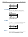
1
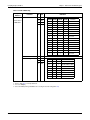
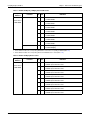
Computing Engines
EP405 1.5 (DES0162)
User Manual
Developing Embedded Applications and Products
Utilizing IBM® PowerPC® 4xx Processors
700M0067RC1
2
700M0067RC1
Computing Engines, EP405 1.5
Copyright
Copyright © 2004 Embedded Planet, LLC. All Rights Reserved.
This manual is copyrighted by Embedded Planet, LLC. No part of this document
may be copied or reproduced in any form or by any means without the express
written permission of Embedded Planet, LLC.
Notice
Embedded Planet, LLC., reserves the right to modify the information contained
herein as necessary and the customer should ensure that it has the most recent
revision of the document. Embedded Planet assumes no responsibility for any
errors which may appear in this document.
This manual in whole or in part, is to be considered the intellectual property of
Embedded Planet. The manual and all information explained and derived there
from are protected by the license to which you agreed upon opening this package.
This document is intended for the sole purpose of the owner of an Embedded
Planet computing engine, to develop applications using PlanetCore. Neither the
document, nor reproductions of it, nor information derived from it is to be given
to others, nor used for any other purpose other than for development of
Embedded Planet computing engine applications, by original, authorized owners
of Embedded Planet products.
Trademarks
Embedded Planet, Linux Planet, Blue Planet, RPX LITE, and RPX LICC are
trademarks or registered trademarks of Embedded Planet.
Freescale and PowerQUICC are trademarks of Freescale Semiconductor, Inc.
IBM and PowerPC are registered trademarks of International Business Machines,
Inc.
Wind River Systems, VxWorks, and Tornado are registered trademarks of Wind
River Systems, Inc.
All other names and trademarks are the property of their respective owners and
are hereby acknowledged.
700M0067RC1
3
Computing Engines, EP405 1.5
4
700M0067RC1
Computing Engines, EP405 1.5
Contents
Chapter 1 Introduction .......................................................................................................... 9
Functions .........................................................................................................................................9
EP405 1.5 Versus EP405 1.3/1.4 .................................................................................................10
How to Use This Manual ............................................................................................................10
Reference Documents ..................................................................................................................11
Chapter 2 Description ......................................................................................................... 13
PowerPC Processor ......................................................................................................................16
EBC Bus Expansion ......................................................................................................................16
SDRAM Organization .................................................................................................................17
FLASH Organization ...................................................................................................................17
I/O Interface Signals ....................................................................................................................19
PlanetCore .....................................................................................................................................20
Chapter 3 Setup ................................................................................................................... 21
Jumpers ..........................................................................................................................................21
Straps ..............................................................................................................................................21
Dipswitch ......................................................................................................................................22
Chapter 4 Connectors and Headers ................................................................................... 23
Power .............................................................................................................................................23
Power Connector ...................................................................................................................23
Expansion Card .....................................................................................................................23
Earth Ground ................................................................................................................................24
JTAG/Debug Port ........................................................................................................................24
TRACE Port ...................................................................................................................................24
Fast Ethernet Port .........................................................................................................................25
Serial Port 0 ...................................................................................................................................25
Serial Port 1 ...................................................................................................................................25
PC/104-Plus Connector ...............................................................................................................26
EBC Bus Expansion Connector ..................................................................................................26
Chapter 5 Operation ............................................................................................................ 31
Board LEDs ...................................................................................................................................31
Fast Ethernet Port LEDs ..............................................................................................................31
PlanetCore Utilities ......................................................................................................................31
RS-232 Connection ................................................................................................................32
User Applications .................................................................................................................32
Chapter 6 Chip Select Programming ................................................................................. 33
FLASH Chip Select Setup ...........................................................................................................33
NVRTC and BCSR Chip Select Setup ........................................................................................34
Chapter 7 Board Control and Status Registers ................................................................ 37
Chapter 8 SDRAM Programming ........................................................................................ 47
Initialization ..................................................................................................................................47
Controller Register Setup ............................................................................................................47
700M0067RC1
5
Computing Engines, EP405 1.5
Contents (continued)
Chapter 9 I2C Devices and Addressing ............................................................................. 51
SEP Format and Interface Structure ..........................................................................................51
STTM Format and Interface Structure ......................................................................................51
Chapter 10 Interrupt Structure ........................................................................................... 53
Appendix A Mechanical Dimensions ................................................................................. 55
List of Figures
No.
2-1.
2-2.
2-3.
2-4.
4-1.
4-2.
A-1.
A-2.
A-3.
A-4.
Title
Page
Simplified Block Diagram .............................................................................................13
EP405 Board - Top View.................................................................................................14
EP405 Board - Bottom View ..........................................................................................15
FLASH Address and Data Lines...................................................................................18
EBC Bus Expansion Connector (P1/P10) Pinout .......................................................28
EBC Bus Expansion Connector (P2/P11) Pinout .......................................................29
EP405 Board - Mechanical (Top) ...................................................................................56
EP405 Board - Mechanicals (Bottom) ...........................................................................57
EP405 Board - Mechanicals (Front and Back) .............................................................58
Straight and Right-Angle Pin Dimensions..................................................................58
List of Tables
No.
1-1.
1-2.
2-1.
2-2.
3-1.
3-2.
3-3.
4-1.
4-2.
4-3.
4-4.
4-5.
5-1.
5-2.
6-1.
6-2.
6
Title
Page
Hardware Features ...........................................................................................................9
Reference Documents.....................................................................................................11
FLASH Devices ...............................................................................................................18
I/O Signals.......................................................................................................................19
JP1 Jumper .......................................................................................................................21
Strap Settings...................................................................................................................21
Dipswitch (SW1) Settings ..............................................................................................22
JTAG/Debug Port Pinout (P3)......................................................................................24
TRACE Port Pinout (P4) ................................................................................................24
Fast Ethernet Port Pinout (P5).......................................................................................25
Serial Port 0 Pinout (P6) .................................................................................................25
Serial Port 1 Pinout (P7) .................................................................................................26
Board LED Definition.....................................................................................................31
Fast Ethernet Port LEDs.................................................................................................31
Chip Select Mapping ......................................................................................................33
FLASH Peripheral Bank Configuration Register (EBC0_BnCR) .............................33
700M0067RC1
Computing Engines, EP405 1.5
List of Tables (continued)
No.
6-3.
6-4.
6-5.
7-1.
7-2.
7-3.
7-4.
7-5.
7-6.
7-7.
7-8.
7-9.
7-10.
7-11.
7-12.
7-13.
7-14.
7-15.
8-1.
8-2.
8-3.
8-4.
8-5.
8-6.
9-1.
10-1.
700M0067RC1
Title
Page
FLASH Peripheral Bank Access Parameters (EBC0_BnAP) .....................................34
NVRTC/BCSR Peripheral Bank Configuration Register (EBC0_B4CR) ................34
NVRTC/BCSR Peripheral Bank Access Parameters (EBC0_B4AP) ........................35
BCSR0 - Board ID............................................................................................................37
BCSR1 - PCI Control and Status ...................................................................................38
BCSR2 - FLASH, NVRAM, and POR Control and Status.........................................38
BCSR3 - FENET and UART Control ............................................................................39
BCSR4 - PCI Status and Masking .................................................................................39
BCSR5 - XIRQ Select.......................................................................................................40
BCSR6 - XIRQ Routing...................................................................................................41
BCSR7 - XIRQ Status (Onboard)...................................................................................42
BCSR8 - XIRQ Status (External)....................................................................................42
BCSR9 - Switch Status and LED Control.....................................................................42
BCSR10 - GPIO[17:23] or IRQ[0:6] Select and PAR Control .....................................43
BCSR11 - GPIO[1:8] Direction Control ........................................................................43
BCSR12 - GPIO[9:16] Direction Control ......................................................................44
BCSR13 - GPIO[17:23] Direction Control ....................................................................44
BCSR15 - CPLD Code Revision ....................................................................................45
SDRAM Configuration Register (SDRAM0_CFG) ....................................................47
SDRAM Memory Bank Configuration Registers (SDRAM0_B0CR).......................48
SDRAM Timing Register (SDRAM0_TR)....................................................................48
SDRAM Refresh Timer Register (SDRAM0_RTR).....................................................49
SDRAM ECC Configuration Register (SDRAM0_ECCCFG) ...................................49
SDRAM Power Management Idle Timer (SDRAM0_PMIT)....................................49
I2C Address Map ............................................................................................................51
Interrupts .........................................................................................................................53
7
Computing Engines, EP405 1.5
8
700M0067RC1
Introduction
Chapter 1
The EP405 board is a highly integrated single-board computer (SBC) based on the
IBM PowerPC 405GP or 405GPr processor. The EP board is in a PC/104-Plus
board mechanical form factor and provides for PCI bus interface. It does not contain ISA functionality directly; an add-on expansion card can provide the ISA bus
interface.
Functions
The functions included on the EP405 are listed in Table 1-1.
Table 1-1. Hardware Features
Entity
Function
Processor
PPC405GP (up to 200 MHz) or
PPC405GPr (up to 400 MHz)
SDRAM1
16, 32, 64, 128 MBytes
FLASH
4, 8, 16, 32, 64 MBytes
NVRTC
0, 32, 128, 512 KBytes
Top 16 bytes are the real-time clock (RTC)
Ethernet port
10BaseT/100BaseTX (RJ-45)
Serial port (RS-232)
UART0 - 9-wire, full modem control (2 × 5 header)
PCI
PC/104-Plus connector
UART1 - 5-wire interface (2 × 5 header)
33 MHz PCI SYNC (synchronous) or 66 MHz PCI
ASYNC (asynchronous) clocking modes supported
Serial EEPROM
I2C
Serial temperature and thermal
monitor
I2C
Debug
JTAG - RiscWatch for BDM
Dipswitch
4-position slide switch read via status register
TRACE - RiscTrace for BDM
LED
4-user programmable via control register
2
Bus expansion
700M0067RC1
Processor bus (EBC) expansion receptacle
I/O expansion
PCI interface via the PC/104-Plus specification
5 VDC supply4
Single power supply source
(board draws 1.5 A maximum)
Operating temperature3
0° C to 70° C (32° C to 158° F)
9
Chapter 1 - Introduction
Computing Engines, EP405 1.5
Table 1-1. Hardware Features (continued)
Entity
BCSR
Function
Board control and status registers
NOTES:
1. With optional error checking and correction (ECC).
2. The bus expansion receptacle allows add-on cards to interface to the processor’s EBC bus. The
expansion receptacle also includes the I2C bus.
3. Contact Embedded Planet for information about industrial temperature version board.
4. The means of disconnection from the mains power supply is the plug.
5. No serviceable parts.
EP405 1.5 Versus EP405 1.3/1.4
This section explains the differences between the EP405 1.5 board and the
EP405 1.3/1.4 boards.
SDRAM
EBC
The option for ECC memory was added to the EP405 1.5 board. This is a build
option for the board.
The PCIINT/PerWE signal was added to the EBC bus connector (P1/P10) of the
EP405 1.5 board. The EBC pinout has not changed from the EP405 1.3/1.4 boards
to the EP405 1.5 board except for this added signal. The EBC connector reference
designators and connector pin numbering have changed on the EP405 1.5 board
silk-screen. Refer to Figure 4-1.
Some EBC signals on the EP405 1.5 board no longer go through the CPLD. In the
documentation, signals that go through the CPLD are identified with an x_ prefix.
The x_ has been removed in the EP405 1.5 board documentation for those signals
that now connect directly to the processor.
FLASH
The EP405 1.5 board supports up to 64 MBytes of FLASH memory using AMD
MirrorBit™ FLASH devices. The FLASH configuration is one bank and two
FLASH devices; refer to Figure 2-4. Each FLASH device is configured for 16-bit
mode (BYTE = 3.3 VDC).
The EP405 1.3/1.4 boards support up to 32 MBytes of FLASH memory. The
FLASH configuration is two banks (address decoding performed in CPLD) and
four FLASH devices (two devices per bank). Each FLASH device is configured for
16-bit mode (BYTE = 3.3 VDC).
Clocking
The PLL clock driver (Cypress W185) on the EP405 1.3/1.4 boards has been
replaced by an MPC9446 clock buffer on the EP405 1.5 board. As a result, spread
spectrum clocking is no longer supported.
Dipswitch
The EP405 1.5 board uses a smaller dipswitch than the EP405 1.3/1.4 boards. Also
the location of the dipswitch has changed. Refer to Figure 2-3.
Jumper
A jumper (JP1) was added to configure the COP/JTAG port. Refer to Table 3-1.
How to Use This Manual
1.
10
Refer to Chapter 2 for a description of the board features and functions.
700M0067RC1
Computing Engines, EP405 1.5
Chapter 1 - Introduction
2. Refer to Chapter 3 for setup information including option straps and
dipswitch settings.
3. Refer to Chapter 4 for a description of the connectors and headers available
on the board.
4. Refer to Chapter 5 for a description of the LED indications for the board and
Ethernet port.
5.
Refer to Chapter 6 for chip select information.
6. Refer to Chapter 7 for board control and status register (BCSR) programming
information.
7.
Refer to Chapter 8 for SDRAM programming information.
8.
Refer to Chapter 9 for programming information for the onboard I2C devices.
9. Refer to Chapter 10 for information about the possible interrupts and interrupt routing.
Reference Documents
Table 1-2 lists additional Embedded Planet documents for the EP board.
Table 1-2. Reference Documents
Document
Number
700M0070R__
700M0067RC1
Description
PlanetCore (PPC4xx), Boot Loader
700M0071R__
PlanetCore (PPC4xx), FLASH Burner
700M0079R__
PlanetCore (PPC4xx), Diagnostics and Utilities
11
Computing Engines, EP405 1.5
12
700M0067RC1
Description
Chapter 2
This chapter provides some description of the EP405 board features including the
PowerPC processor, external interfaces, bus expansion, and PlanetCore.
Figure 2-1 is a simplified block diagram of the EP board. Figures 2-2 and 2-3 show
the top and bottom view board layouts. These figures show the headers unpopulated (i.e., without pins or connectors).
NVRTC
SDRAM
FLASH
EXTERNAL BUS (EBC/SDRAM)
I2C
BCSR
SWITCH
SEP
PPC405GP/GPr
SW1
STTM
CLOCK
LED0/1/2/3
UART0
JTAG
(P3)
UART1
RS-232
RS-232
FENET
SERIAL 0
(P6)
SERIAL 1
(P7)
10BASET/
100BASETX
(P5)
PCI
PC/104-PLUS
(P8)
TRACE
(P4)
EBC BUS
EXPANSION
(P1, P2, P10, P11)
T00101C
Figure 2-1. Simplified Block Diagram
PPC405GP/GPr
Clocking
Refer to PowerPC Processor in this chapter.
The system clock, or SysClk on the EP board, is supplied from an MPC9446 Clock
Fanout Buffer device. The input to the clock buffer device is a 66.67 MHz oscillator.
During hard reset the board is configured for either PCI synchronous clocking
mode or PCI asynchronous clocking mode depending on the M66EN signal of the
PCI bus. The MPC9446 device on the board provides the system clock input
(SysClk) to the processor at 33 MHz. For 33 MHz PCI synchronous clocking operation the PCI bus clock is the system clock input. For 66 MHz PCI asynchronous
clocking operation the PCI bus clock is the PCI clock input (PciClk) to the processor sourced from the MPC9446 device at 66 MHz.
700M0067RC1
13
Chapter 2 - Description
Computing Engines, EP405 1.5
RESET
POWER
EBC EXPANSION
A1
A1
P9
S4
JTAG
P2
1
E1
E1
P1
JP1
A1
E1
P3
PC/104-PLUS
TRACE
1
P8
P4
ROA10
P5
ROB10
P6
1
SERIAL PORT 0
P7
1
10BASET/100BASETX
ETHERNET
SERIAL PORT 1
T00106C
Figure 2-2. EP405 Board - Top View
14
Memory
The board can be ordered with a variety of memory configurations and optionally
supports ECC memory (Table 1-1): SDRAM (Micron/Samsung; refer to SDRAM
Organization in this chapter), FLASH (AMD: AM29DLxxxM/AM29LVxxxM),
and NVRAM (Dallas Semiconductor: DS13xx/DS15xx).
BCSR
Board control and status registers (BCSR) provide hardware control and status to
the processor. BCSR bits selectively enable/disable and configure board features,
and control LEDs, read switch settings (SW1), and provide status indications. The
BCSR registers of the EP boards are implemented in control logic within a complex programmable logic device (CPLD). Refer to the Chapter 7 for BCSR programming information.
SEP
The serial EEPROM (SEP) stores configuration parameters for the board. These
configuration parameters are set using PlanetCore; refer to PlanetCore in this
chapter. The SEP part is a 2-wire, serial EEPROM. Its functionality is equivalent to
the Atmel AT24C04 part. Refer to the Chapter 9 for programming information for
this I2C device.
700M0067RC1
Computing Engines, EP405 1.5
Chapter 2 - Description
E1
E1
A1
A1
RO12
RO1
RO6
SW1
RO7
CR1
CR0 CR2
LEDS
CR3
T00107C
Figure 2-3. EP405 Board - Bottom View
STTM
I/O
The serial temperature and thermal monitor (STTM) is an onboard temperature
sensor. The STTM part is a 2-wire, digital temperature sensor. Its functionality is
equivalent to the Microchip TCN75 part. The minimum resolution provided by
this part is a 9-bit temperature conversion. Refer to the Chapter 9 for programming information for this I2C device.
The EP board has:
•
One fast Ethernet port (P5). This port uses a Level One LXT971A Ethernet
transceiver. The port connects to the MII port of the processor. Communication is via the MII management port. The fast Ethernet PHY address is either
0b00000 (default) or 0b00001 depending on strapping option (Table 3-2).
•
Two serial port headers (P6 and P7). The ports use UART0 and UART1 of the
processor. The serial ports use Maxim MAX3245E RS-232 transceivers or
equivalent.
•
One JTAG port header (P3) with right-angle connector for debugger use.
•
One TRACE port header (P4) with right-angle connector for debugger use.
Refer to Chapter 4 for more information and pinouts for the connectors.
EBC Bus Expansion
700M0067RC1
The EBC bus from the processor’s external bus controller is brought out to the
EBC bus expansion connector (P1/P10, P2/P11) on the board. This allows interfacing add-on boards to the processor. The I2C bus is also routed to the connector.
15
Chapter 2 - Description
Computing Engines, EP405 1.5
PCI
The PCI bus from the processor’s PCI interface is brought out to the PC/104-Plus
connector (P8). The PPC405GP/GPr processor provides the host PCI bridge (commonly referred to as North Bridge) and a PCI arbiter.
Interrupt Control
There is onboard IRQ routing and status features implemented in a CPLD that can
be enabled or disabled by setting bits in a BCSR register. This along with the interrupt controller of the processor provide board and PCI interrupt request control.
If desired an add-on board can provide the PCI IRQ controller along with a
PCI-to-ISA bridge (commonly referred to as South Bridge).
NOTE: The EP405 board supports PCI host mode only.
PowerPC Processor
The EP board incorporates an IBM PowerPC 405GP or 405GPr embedded processor. This 32-bit reduced instruction set computer (RISC) processor includes an
integrated PowerPC core and peripheral interfaces that can be used in a variety of
controller applications. It is particularly well-suited for both communications and
networking applications. The PPC405GP/GPr provides high performance and
low power consumption.
The processor has integrated peripheral functions for I/O interface, which
include:
•
•
•
•
•
•
•
•
SDRAM controller.
External bus controller (EBC).
PCI bus interface.
Direct memory access (DMA).
Ethernet and media access layer (MAL) interfaces.
Two serial ports.
Inter-integrated circuit (I2C) interface.
General-purpose I/O (GPIO).
EBC Bus Expansion
The EBC Expansion Bus connectors are two 5 × 20, high-density surface-mount
connectors. This interface, along with the PCI bus interface, allow I/O expansion
cards to be designed and interfaced to the EP board. Most peripheral signals are
routed to the connectors for processor interface. Refer to Figures 2-2 and 2-3 for
the connector locations and EBC Bus Expansion Connector in Chapter 4 for connector pinouts.
The P1/P10, P2/P11 connectors give access to numerous CPU external signal
lines including some of the following interface signals:
•
•
•
•
•
•
•
•
•
16
Peripheral bus clock - PerClk
Peripheral address bus - PerAddr0:31
Peripheral data bus - PerData0:31
Peripheral parity bus - PerPar0:3
Chip selects - PerCS0:7
Read not write - PerR/W
Write byte enables or read/write byte enables - PerWBE0:3
Output enable - PerOE
Write enable - PerWE
700M0067RC1
Computing Engines, EP405 1.5
Chapter 2 - Description
•
•
•
•
•
Peripheral data error input - PerErr
External interrupt - IRQ0:6
General purpose I/O - GPIO0:23
I2C serial clock - I2CSCL
I2C serial data - I2CSDA
SDRAM Organization
Paged-based SDRAM
Memory Clock
MemClkOut1:0 = 100 MHz or 133 MHz
16 MByte
64 Mbit (4M x 16 bit) devices
2 Micron MT48LC4M16A2TG-8E/75
2 MBytes x 4 banks x 2 devices = 16 MBytes total
2 bit bank address at A[8:9]
12 bit row address at A[10:21]
8 bit column address at A[22:29]
32 MByte
128 Mbit (8M x 16 bit) devices
2 Micron MT48LC8M16A2TG-8E/75
4 MBytes x 4 banks x 2 devices = 32 MBytes total
2 bit bank address at A[7:8]
12 bit row address at A[9:20]
9 bit column address at A[21:29]
64 MByte
256 Mbit (16M x 16 bit) devices
2 Micron MT48LC16M16A2TG-7E/75
8 MBytes x 4 banks x 2 devices = 64 MBytes total
2 bit bank address at A[6:7]
13 bit row address at A[8:20]
9 bit column address at A[21:29]
128 MByte
512 Mbit (32M x 16 bit) devices
2 Micron MT48LC32M16A2TG-7E/75
16 MBytes x 4 banks x 2 devices = 128 MBytes total
2 bit bank address at A[6:7]
13 bit row address at A[8:20]
10 bit column address at A[5,21:29]
FLASH Organization
This section summarizes the FLASH memory devices currently used on the EP
board. Refer to the AMD data sheets for detailed information about these FLASH
memory devices. Figure 2-4 shows the address and data line connections. An offset is needed when issuing commands to the FLASH devices due to the address
line connections.
Table 2-1 lists the FLASH memory devices and their device IDs. Command codes
for all devices are the same. Device ID varies among the different devices. Sector
addresses also vary among the different devices.
700M0067RC1
17
Chapter 2 - Description
Computing Engines, EP405 1.5
D[0..31]
A[0..31]
U8
A29
A28
A27
A26
A25
A24
A23
A22
A21
A20
A19
A18
A17
A16
A15
A14
A13
A12
A11
A10
A9
A8
A7
A6
+3.3V
CS0n
A0
A1
A2
A3
A4
A5
A6
A7
A8
A9
A10
A11
A12
A13
A14
A15
A16
A17
A18
A19
A20
A21
A22
A23
WP#ACC
DQ0
DQ1
DQ2
DQ3
DQ4
DQ5
DQ6
DQ7
DQ8
DQ9
DQ10
DQ11
DQ12
DQ13
DQ14
DQ15/A-1
D1 5
D1 4
D1 3
D1 2
D1 1
D1 0
D9
D8
D7
D6
D5
D4
D3
D2
D1
D0
RY/BY#
BYTE#
CE#
OE#
WE#
RESET#
U9
A29
A28
A27
A26
A25
A24
A23
A22
A21
A20
A19
A18
A17
A16
A15
A14
A13
A12
A11
A10
A9
A8
A7
A6
+3.3V
A0
A1
A2
A3
A4
A5
A6
A7
A8
A9
A10
A11
A12
A13
A14
A15
A16
A17
A18
A19
A20
A21
A22
A23
WP#ACC
DQ0
DQ1
DQ2
DQ3
DQ4
DQ5
DQ6
DQ7
DQ8
DQ9
DQ10
DQ11
DQ12
DQ13
DQ14
DQ15/A-1
D3 1
D3 0
D2 9
D2 8
D2 7
D2 6
D2 5
D2 4
D2 3
D2 2
D2 1
D2 0
D1 9
D1 8
D1 7
D1 6
RY/BY#
BYTE#
CE#
OE#
WE#
RESET#
T00157B
Figure 2-4. FLASH Address and Data Lines
Table 2-1. FLASH Devices
Device
18
MFG ID
Device ID
AM29LV160MB
0001
2249
AM29LV320ML
0001
227E, 221D, 2200
AM29LV640ML
0001
227E, 220C, 2201
AM29LV128ML
0001
227E, 2212, 2200
AM29LV256ML
0001
227E, 2212, 2201
700M0067RC1
Computing Engines, EP405 1.5
Chapter 2 - Description
The following guidelines apply to x32 ported FLASH memory:
FLASH devices configured in 16-bit mode.
Sector and chip erases should be performed only on a long word basis.
Programming should be done on a long word basis if possible.
One bank of FLASH with contiguous address space.
•
•
•
•
I/O Interface Signals
Table 2-2 lists the I/O interface signals used on the EP board.
Table 2-2. I/O Signals
Interface
Serial ports
Signal
UART0_DCD
UART0_DSR
UART0_DTR
UART0_RI
UART0_RTS
UART0_Rx
UART0_Tx
[UART1_CTS]UART1_DSR
[UART1_DTR]UART1_RTS
UART1_Rx
UART1_Tx
Ethernet
EMCMDIO[PHYMDIO]
EMCTxD0
EMCTxD1
EMCTxD2
EMCTxD3
EMCTxEn
EMCTxErr
PHYCol
PHYCrS
PHYRxClk
PHYRxD0
PHYRxD1
PHYRxD2
PHYRxD3
PHYRxDV
PHYRxErr
PHYTxClk
I
2C
IICSCL
IICSDA
700M0067RC1
19
Chapter 2 - Description
Computing Engines, EP405 1.5
PlanetCore
PlanetCore consists of:
•
•
Target based application boot loader.
Host based FLASH burner.
PlanetCore is included with each Embedded Planet software development platform and computing engine.
The EP board is shipped with the boot loader program residing in FLASH memory. The boot loader utilities provide the ability to initialize the CPU board and
auto execute an operating system or application. Refer to the PlanetCore User
Manuals for complete information about these utilities.
Boot Loader
The boot loader has the following features and benefits:
•
•
•
•
•
•
•
•
•
Diagnostics and
Utilities
The diagnostics and utilities have the following features and benefits:
•
•
•
•
FLASH Burner
Small memory footprint (< 256KB).
Boots quickly.
Can optionally test the DRAM during startup.
Command line interface via monitor port – has online help.
Configured via EEPROM settings.
Robust serial and Ethernet (tftp) communications and data transfers.
Can download s-record or binary images.
Can boot user applications from FLASH or via TFTP.
Diagnostic tests: memory (FLASH, DRAM, NVRAM) and Ethernet.
Diagnostics are available for CPU board testing.
Can be removed if not needed to free up FLASH memory space.
Available in RAM version.
Uses monitor port for user interface.
The FLASH burner has the following features and benefits:
•
Resides as a separate program, not resident in FLASH (conserves memory).
•
Can be incorporated into the build process to place programs into FLASH
memory.
•
Erases and programs AMD FLASH memory using a one-step process.
•
FLASH burner image is in an s-record format, loaded by the boot loader or
debugger.
•
Multiple sections of FLASH can be programmed in one file.
To use the FLASH burner, the code can be loaded and executed from the boot
loader, or it can be loaded and executed from a debugger (if no loader is present in
FLASH). Once started, the burner uses the monitor terminal for a user interface.
20
700M0067RC1
Setup
Chapter 3
This chapter describes the various strappings and dipswitch settings that setup
the EP405 board for operation. The straps are zero ohm, surface-mount resistors.
The dipswitch has four positions.
Jumpers
Jumper JP1 configures P3 as either a JTAG port or a COP port. Table 3-1 describes
the jumper settings; refer to Figure 2-2 for the location of the jumper.
Table 3-1. JP1 Jumper
Purpose
Setting
Function
COP
JP1: 2-3
JP1: 5-6
P3 operates in COP mode to support hardware and
software development and debugging.
JTAG (CPLD only)
JP1: 1-2
JP1: 4-5
JTAG chain active at P3. These settings put only the
CPLD in the JTAG chain.
JTAG (complete)
JP1: 1-2
JP1: 3-4
JP1: 5-6
JTAG chain active at P3. These settings complete the
JTAG chain from P3 to the processor, the processor to
the CPLD, then the CPLD to P3.
Straps
Table 3-2 describes the various strap settings; refer to Figures 2-2 and 2-3 for the
locations of the straps.
Table 3-2. Strap Settings
Purpose
Earth ground1
Strap
RO1
Function
Populated = EARTH_GND connected to DIGITAL_GND at one point.
Not populated = EARTH_GND not connected to DIGITAL_GND.
FENET PHY
address
RO6: 1-2
PHY address = 00000
RO6: 1-3
PHY address = 00001
UART1
RO7: 1-2
RS-232 transceiver drives the DTR true all the time (5 VDC minimum at 1.67 mA)
RO7: 1-3
5 VDC rail drives the DTR signal all the time (for powering IR keyboards).
ROA10
3.3 VDC VIO supplied
ROB10
5 VDC VIO supplied
RO12: in
Force 33 MHz operation; M66EN signal low
RO12: out
Normal operation
2
PCI VIO
M66EN signal
NOTES:
1. All mounting holes and shields on connectors are connected together and to EARTH_GND.
2. Only one resistor option populated at a time.
700M0067RC1
21
Chapter 3 - Setup
Computing Engines, EP405 1.5
Dipswitch
The four-pole dipswitch (SW1) located on the board is readable via an onboard
status register (Table 7-10). The switch is intended for user applications, but has
some reserved settings. Table 3-3 describes the switch settings; refer to Figure 2-3
for the location of the dipswitch.
Table 3-3. Dipswitch (SW1) Settings
Pole Positions
Function
1234
D(24:27)
0000 or 1111
Normal operating mode
0001
Reserved for manufacture test
0010
Reserved for fallback mode
0011 through 1110
User specified
NOTE:
down = on = closed position will read back a logic 0 in the status register.
up = off = open position will read back a logic 1 in the status register.
22
700M0067RC1
Connectors and Headers
Chapter 4
The EP405 board has the following connectors for I/O functions and expandability:
•
One RJ-45 connector with integrated LEDs for the fast Ethernet port
(100BaseTX/10BaseT).
•
Two headers for RS-232 serial ports.
•
One barrel connector for power.
•
One EBC bus expansion connector.
•
One PC/104-Plus connector.
•
Two headers for auxiliary functions: JTAG and TRACE.
This chapter describes these connectors and headers. Refer to Figures 2-2 and 2-3
for the locations of these connectors and headers.
Power
There are different options for powering the EP board:
•
5 VDC supplied through the barrel connector. This is the standard option for
powering the board.
•
5 VDC from an expansion card.
The 5 VDC power option requires a regulated 4.75 to 5.25 VDC supply. The EP
board itself, fully configured, but with no expansion cards, draws 1.5 A maximum
at VCC = 4.75 VDC to 5.25 VDC, T = 0° C to 70° C (32° C to 158° F).
Power Connector
The power connector (P9) is a barrel type connector. The specifications for the
mating connector are as follows:
Inner diameter = 2.5 mm (0.100 inches)
Outer diameter = 5.5 mm (0.218 inches)
Barrel Length >/= 9.5 mm (0.375 inches)
Outer shell is GND
Inner shell is 5 VDC
Expansion Card
It is recommended that the supply voltage for an expansion card be derived from
the 5 VDC pins of the expansion connector. This keeps the processor/memory
core, which runs at 3.3 VDC, very clean.
700M0067RC1
23
Chapter 4 - Connectors and Headers
Computing Engines, EP405 1.5
Earth Ground
Earth ground connections are made through the four mounting holes on the EP
board. Earth ground is connected to signal ground in one place on the EP board.
Signal ground can be optionally disconnected from earth ground by removing
RO1 from the EP board (Table 3-2). RO1 is populated by default because the EP
boards are designed to be powered by a wall-cube unit, and wall-cubes supplied
with the units have their grounds (GND) isolated.
Applications must consider how the EP board will be powered, and whether or
not EARTH_GND should be connected to DIGITAL_GND (signal ground) via
RO1 on the EP board. EARTH_GND and DIGITAL_GND should be connected at
only one point in the system. Erratic behavior could occur if ground loops are
induced into the system through multiple connections.
NOTE: All connector housings (e.g., Ethernet, serial, etc.) are connected to EARTH_GND.
JTAG/Debug Port
The JTAG/debug port is P3. It is a 2 × 7 (0.1 × 0.1) header. Table 4-1 shows the
JTAG/debug port pinout.
Table 4-1. JTAG/Debug Port Pinout (P3)
Pin
Function
Pin
Function
1
TDO
2
—
3
TDI
4
TRST
5
—
61
+3.3V
7
TCK
8
—
9
TMS
10
—
11
HALT
12
—
13
—
14
—
15
—
16
GND
NOTE:
1. Current limited with a 1K resistor.
TRACE Port
The TRACE port is P4. It is a 2 × 10 (0.1 × 0.1) header. Table 4-2 shows the TRACE
port pinout.
Table 4-2. TRACE Port Pinout (P4)
Pin
24
Function
Pin
Function
1
—
2
—
3
CLK
4
—
5
—
6
—
7
—
8
—
9
—
10
—
700M0067RC1
Computing Engines, EP405 1.5
Chapter 4 - Connectors and Headers
Table 4-2. TRACE Port Pinout (P4) (continued)
Pin
Function
Pin
Function
11
—
12
TS1O
13
TS2O
14
TS1E
15
TS2E
16
TS3
17
TS4
18
TS5
19
TS6
20
GND
Fast Ethernet Port
The fast Ethernet (10BaseT/100BaseTX) port is connector P5 (FETH). It is a
shielded RJ-45 jack with integrated LEDs. Table 4-3 shows the RJ-45 jack pinout.
The RJ-45 connector is shielded and tied to EARTH GROUND. This Ethernet port
is from the MII.
Table 4-3. Fast Ethernet Port Pinout (P5)
Pin
Function
Pin
Function
1
TXD+
5
—
2
TXD-
6
RXD-
3
RXD+
7
—
4
—
8
—
NOTE:
1. Pin numbering is from right (1) to left (8) when
looking into the RJ-45 jack with the locking tab on
top.
Serial Port 0
The serial port 0 (UART0) is P6. It is a 2 × 5 (0.1 × 0.1) header. Table 4-4 shows the
serial port pinout. The port signals are surge protected with the transient voltage
suppressors connected to EARTH GROUND. The port is wired as DTE.
Table 4-4. Serial Port 0 Pinout (P6)
Pin
Function
Pin
Function
1
DCD
2
DSR
3
RXD
4
RTS
5
TXD
6
CTS
7
DTR
8
RI
9
GND
10
—
Serial Port 1
The serial port 1 (UART1) is P7. It is a 2 × 5 (0.1 × 0.1) header. Table 4-5 shows the
serial port pinout. The port signals are surge protected with the transient voltage
suppressors connected to EARTH GROUND. The port is wired as DTE.
700M0067RC1
25
Chapter 4 - Connectors and Headers
Computing Engines, EP405 1.5
Table 4-5. Serial Port 1 Pinout (P7)
Pin
Function
Pin
Function
1
—
2
—
3
RXD
4
RTS
5
TXD
6
CTS
7
DTR
8
—
9
GND
10
—
NOTE:
1. DTR can be driven, via strapping option
(Table 3-2), by the RTS signal or by the system
5 VDC supply.
PC/104-Plus Connector
The PC/104-Plus connector is P8. It is a standard 4 × 30, 2 millimeter connector as
defined by the PC/104-Plus specification. This interface allows PCI add-on
boards to be designed and interfaced to the EP board. The PC/104-Plus connector
is a through-hole connector, which means it can be populated on the top of the
board only, bottom of the board only, or both top and bottom if desired. Refer to
the PC/104-Plus specification for pinout information.
EBC Bus Expansion Connector
The EBC bus expansion connector consists of P1/P10 and P2/P11. Each is a 5 × 20,
high-density receptacle. This interface allows add-on boards to be designed and
interfaced directly to the EP board through the EBC bus.
EP board to expansion card spacing is not fixed. The connector type chosen
allows for variable stacking heights. The receptacle part number used on the standard product is Samtec YFS-20-03-G-05-SB. Refer to the Samtec Hi-Density
Stacker fact sheet for expansion card mating plug options (YFT-20-xx-y-05-zz or
YFW-20-xx-y-05-zz).
NOTE: W and T are two different styles for the expansion card mating plug; both are compatible with the EP board. The W gives several height options.
The board-to-board spacing can be adjusted by selecting one of the available
Samtec mating connectors and appropriate stand-offs. Stand-offs should be
3/16-inch hex metal stand-offs so that EARTH_GND connections can be made
from the expansion card to the EP board. The stand-offs should also have 4-40
threads to accommodate the 0.125-inch diameter mounting holes in the PCB.
NOTE: Either 16 mm board spacing or cut outs in the expansion card are required to clear the
RJ-45 connectors on the EP board.
Important
26
The EP405 EBC bus expansion connector (P1/P10, P2/P11) interface must be a 3.3
VDC only type of interface (the I/O is not 5 VDC I/O tolerant).
700M0067RC1
Computing Engines, EP405 1.5
Chapter 4 - Connectors and Headers
Refer to Figure 4-1 for the P1/P10 connector pinout and Figure 4-2 for the P2/P11
connector pinout.
NOTE: In Figures 4-1 and 4-2, the n appended to a signal name indicates active low. The x at
the beginning of a signal name means external.
700M0067RC1
27
A4
A5
A6
A7
A8
A9
A10
A11
A12
A13
A14
A15
P1C/P10C
perWEn
E1
E2
E3
E4
E5
E6
E7
E8
E9
E10
E11
E12
E13
E14
E15
E16
E17
E18
E19
E20
+5.0V
+5.0V
+5.0V
C1
C2
C3
C4
C5
C6
C7
C8
C9
C10
C11
C12
C13
C14
C15
C16
C17
C18
C19
C20
P1A/P10E
x_CFG11_GPIO1_TS1E
x_CFG12_GPIO2_TS2E
x_GPIO3_TS1O
x_CFG21_GPIO4_TS2O
x_GPIO5_TS3
x_GPIO6_TS4
x_GPIO7_TS5
x_GPIO8_TS6
x_GPIO9_TRCCLK
x_perCS0n
x_GPIO10_perCS1n
x_GPIO11_perCS2n
x_GPIO12_perCS3n
x_GPIO13_perCS4n
x_GPIO14_perCS5n
x_GPIO15_perCS6n
P1B/P10D
P1D/P10B
D0
D1
D2
D3
D4
D5
D6
D7
D8
D9
D10
D11
D12
D13
D14
D15
D1
D2
D3
D4
D5
D6
D7
D8
D9
D10
D11
D12
D13
D14
D15
D16
D17
D18
D19
D20
A1
A2
A3
A4
A5
A6
A7
A8
A9
A10
A11
A12
A13
A14
A15
A16
A17
A18
A19
A20
Chapter 4 - Connectors and Headers
28
P1E/P10A
A0
A1
A2
A3
EOT0_TC0
EOT1_TC1
EOT2_TC2
EOT3_TC3
perCS0n
perERR
perCLK
perOEn
perR_Wn
perBLASTn
perREADY
B1
B2
B3
B4
B5
B6
B7
B8
B9
B10
B11
B12
B13
B14
B15
B16
B17
B18
B19
B20
T00103B
Figure 4-1. EBC Bus Expansion Connector (P1/P10) Pinout
Computing Engines, EP405 1.5
700M0067RC1
A20
A21
A22
A23
A24
A25
A26
A27
A28
A29
A30
A31
P2C/P11C
E1
E2
E3
E4
E5
E6
E7
E8
E9
E10
E11
E12
E13
E14
E15
E16
E17
E18
E19
E20
+5.0V
+5.0V
( To CPLD)
CS0L_CS0Xn
CLKSYNC
I2CSDA
I2CSCL
C1
C2
C3
C4
C5
C6
C7
C8
C9
C10
C11
C12
C13
C14
C15
C16
C17
C18
C19
C20
P2AP11E
x_GPIO16_perCS7n
x_GPIO17 _IRQ0
x_GPIO18 _IRQ1
x_GPIO19 _IRQ2
x_GPIO20 _IRQ3
x_GPIO21 _IRQ4
x_GPIO22 _IRQ5
x_GPIO23 _IRQ6
x_GPIO24_legacy_newmode
CFG0_dmaACK0
CFG1_dmaACK1
CFG2_dmaACK2
CFG3_dmaACK3
P2D/P11B
D16
D17
D18
D19
D20
D21
D22
D23
D24
D25
D26
D27
D28
D29
D30
D31
D1
D2
D3
D4
D5
D6
D7
D8
D9
D10
D11
D12
D13
D14
D15
D16
D17
D18
D19
D20
dmaREQ0
dmaREQ1
dmaREQ2
dmaREQ3
A1
A2
A3
A4
A5
A6
A7
A8
A9
A10
A11
A12
A13
A14
A15
A16
A17
A18
A19
A20
Computing Engines, EP405 1.5
700M0067RC1
P2E/P11A
A16
A17
A18
A19
P2B/P11D
perWBE0n
perWBE1n
perWBE2n
perWBE3n
HOLDREQ
CFG17_HOLDACK
EXTREQn
CFG19_EXTACKn
XRSTn
x_PAR0
x_PAR1
x_PAR2
x_PAR3
HOLDPRI
BUSREQ
perEXTRSTn
( To CPLD)
B1
B2
B3
B4
B5
B6
B7
B8
B9
B10
B11
B12
B13
B14
B15
B16
B17
B18
B19
B20
T00110B
Figure 4-2. EBC Bus Expansion Connector (P2/P11) Pinout
Chapter 4 - Connectors and Headers
29
Computing Engines, EP405 1.5
30
700M0067RC1
Operation
Chapter 5
This chapter describes the LED indications for the EP405 board. It also provides
some PlanetCore description and communication information.
Board LEDs
The four user-programmable LEDs (Table 5-1) are under BCSR control. Refer to
Table 7-10 for LED control bit information. Refer to Figure 2-3 for the locations of
the LEDs.
Table 5-1. Board LED Definition
LED
Signal
CR0
LED0
CR1
LED1
CR2
LED2
CR3
LED3
Color
Red
Fast Ethernet Port LEDs
Table 5-2 describes the indications given by the fast Ethernet port LEDs (P5); refer
to Figure 2-2 for the location of the port. These LEDs are integrated into the Ethernet port.
Table 5-2. Fast Ethernet Port LEDs
State
Indication
Left LED (LED2)
Right LED (LED1)
Off
Link integrity bad
No RXD or TXD activity
Yellow
Link integrity good and
10 Mbps Ethernet
RXD or TXD activity and
half-duplex Ethernet
Green
Link integrity good and
100 Mbps Ethernet
RXD or TXD activity and
full-duplex Ethernet
PlanetCore Utilities
The EP board, in its simplest form, is shipped with the PlanetCore boot loader
software; refer to PlanetCore in Chapter 2. This code verifies the integrity of the
hardware, allows configuration changes, and allows downloading of user code.
As additional functions are added, the program will be updated and made available from Embedded Planet. Upgrades are provided as files containing Freescale
s-records. The s-record data is a program which is downloaded to RAM either
using one of the two serial ports and a terminal emulation program, or using the
700M0067RC1
31
Chapter 5 - Operation
Computing Engines, EP405 1.5
Ethernet port and a TFTP server. Once downloaded, the program runs and
replaces the regions of FLASH containing the current code.
Refer to the PlanetCore User Manuals for information about the PlanetCore boot
loader, FLASH burner, and diagnostics and utilities.
RS-232 Connection
A 2 × 5 header to DB-9 (or DB-25) connection is required for RS-232 communication. Tables 4-4 and 4-5 provide the pinouts for the headers. The EP board has its
serial ports wired as DTE. A null modem type of connection is required when
interfacing to a DTE port.
For DTE:
DB9-3 = TXD
DB9-2 = RXD
DB9-8 = CTS
DB9-7 = RTS
DB9-5 = GND
DB25-2 = TXD
DB25-3 = RXD
DB25-5 = CTS
DB25-4 = RTS
DB25-7 = GND
User Applications
PlanetCore assumes the board is connected to a dumb terminal or a PC-based terminal emulator, and requires user intervention for the diagnostics. The dumb terminal or PC serial port should be set as follows:
•
•
•
•
•
9600 baud (default).
8 data bits.
1 stop bit.
No parity.
No hardware handshake.
Proper interfacing to the serial port via the correct RS-232 connections must be
insured as described in RS-232 Connection in this chapter. The dumb terminal or
PC serial port might require the CTS signal to be true. In this case, the RTS signal,
which is driven true from the serial port, should also be connected in the cable
path to the CTS signal on the dumb terminal or PC serial port.
32
700M0067RC1
Chip Select Programming
Chapter 6
Table 6-1 contains the chip select mapping for the EP405 board.
Table 6-1. Chip Select Mapping
Chip
Select
Bus
CS0
32-bit
Function/Address
FLASH
Comment
4, 8, 16, 32, 64 MBytes
FFFF FFFF minus actual
FLASH size
CS1
—
Unused
—
CS2
—
Unused
—
CS3
—
Unused
—
CS4
8-bit
Control and status registers
F400 0000
BCSR - 16 bytes (512K space
decoded)
NVRTC
F420 0000
0, 32, 128, or 512 KBytes
(Top 16 bytes are the RTC)
CS5
—
Unused
—
CS6
—
Unused
—
CS7
—
Unused
Can be used to access FLASH if
CS0 is used for expansion FLASH.
Refer to BCSR2 information
(Table 7-3).
NOTE:
1. All chip selects are available at the EBC expansion receptacle (P1/P10, P2/P11).
FLASH Chip Select Setup
Software must program two EBC registers for FLASH memory chip select configuration:
•
•
Peripheral Bank Configuration Register (EBC0_B0CR or EBC0_B7CR).
Peripheral Bank Access Parameters (EBC0_B0AP or EBC0_B7AP).
The FLASH memory can use either PerCS0 or PerCS7 depending on BCSR2
(Table 7-3). PerClk is 50 MHz. The register settings are for a 64 MByte block and
based on 70 nsec FLASH.
Table 6-2. FLASH Peripheral Bank Configuration Register (EBC0_BnCR)
Bit
Field
Value
BAS
12:14
BS
110
64 MByte bank
15:16
BU
11
read/write
700M0067RC1
0xFC0
Description
0:11
Base address select. Specifies the bank starting address. The bank starting
address must be a multiple of the bank size programmed in the BS field.
33
Chapter 6 - Chip Select Programming
Computing Engines, EP405 1.5
Table 6-2. FLASH Peripheral Bank Configuration Register (EBC0_BnCR) (continued)
Bit
Field
Value
Description
17:18
BW
10
32-bit bus
19:31
Reserved
—
Leave at reset state.
NOTE: At POR, EBC0_B0CR = 0xffe28000 (2 MByte read only).
Table 6-3. FLASH Peripheral Bank Access Parameters (EBC0_BnAP)
Bit
Field
Value
0
BME
0
00000100
Description
Bursting disabled
1:8
TWT
9:11
Reserved
—
Leave at reset state.
12:13
CSN
00
Chip select on timing = 0 PerClk cycles
14:15
OEN
00
Output enable on timing = 0 PerClk cycles
16:17
WBN
00
Write byte enable on timing = 0 PerClk cycles
18:19
WBF
00
Write byte enable off timing = 0 PerClk cycles
20:22
TH
000
Transfer hold = 0 PerClk cycles
23
RE
0
24
SOR
0
Sample on ready = PerReady disabled
25
BEM
0
timing = active for only write cycles.
26
PEN
0
Disable parity checking
Reserved
—
Leave at reset state.
27:31
Transfer wait = 4 PerClk cycles
Disable PerReady
NOTE: At POR, EBC0_B0AP=0x7f8ffe80 (slowest possible bus timings).
NVRTC and BCSR Chip Select Setup
Software must program two EBC registers for NVRTC and BCSR chip select configuration:
Peripheral Bank Configuration Register (EBC0_B4CR).
Peripheral Bank Access Parameters (EBC0_B4AP).
•
•
The NVRTC and BCSR share PerCS4. PerClk is 50 MHz. The register settings are
for a 4 MByte block and based on 150 nsec NVRAM.
Table 6-4. NVRTC/BCSR Peripheral Bank Configuration Register (EBC0_B4CR)
Bit
34
Field
Value
0xF40
Description
0:11
BAS
Base address select. Specifies the bank starting address. The bank starting
address must be a multiple of the bank size programmed in the BS field.
12:14
BS
010
4 MByte bank
15:16
BU
11
read/write
17:18
BW
00
8-bit bus
19:31
Reserved
—
Leave at reset state.
700M0067RC1
Computing Engines, EP405 1.5
Chapter 6 - Chip Select Programming
Table 6-5. NVRTC/BCSR Peripheral Bank Access Parameters (EBC0_B4AP)
Bit
Field
Value
Description
0
BME
0
1:8
TWT
00001000
Bursting disabled
9:11
Reserved
—
Leave at reset state.
12:13
CSN
01
Chip select on timing = 1 PerClk cycle
Transfer wait = 8 PerClk cycles
14:15
OEN
01
Output enable on timing = PerOE one PerClk cycle after PerCS4
16:17
WBN
00
Write byte enable on timing = 0 PerClk cycles
18:19
WBF
00
Write byte enable off timing = 0 PerClk cycles
20:22
TH
000
Transfer hold = 0 PerClk cycles
23
RE
0
Disable PerReady
24
SOR
0
Sample on ready = PerReady disabled
25
BEM
0
timing = active for only write cycles.
26
PEN
0
Disable parity checking
Reserved
—
Leave at reset state.
27:31
700M0067RC1
35
Computing Engines, EP405 1.5
36
700M0067RC1
Board Control and Status Registers
Chapter 7
The EP405 board has onboard control and status registers. These registers are configured as x8 ports. The registers are defined as shown in Tables 7-1 through 7-15.
Register values at reset (values in binary):
Register 0 = ID
Register 1 = 0000 0000
Register 2 = 0000 0000
Register 3 = 0000 1111
Register 4 = 0000 1111
Register 5 = 0000 0000
Register 6 = 0000 0111
Register 7 = 0000 0000
Register 8 = 0000 0000
Register 9 = uuuu 0000
Register 10 = 0000 0000
Register 11 = 0000 0000
Register 12 = 0000 0000
Register 13 = 0000 0000
Register 14 = Reserved
Register 15 = Revision
Board ID
PCI control and status
FLASH, NVRAM, and POR control and status
FENET and UART control
PCI status and masking
XIRQ select
XIRQ routing
XIRQ status (onboard)
XIRQ status (external)
Switch status (uuuu = dipswitch setting) and LED
control
GPIO[17:23] or XIRQ[0:6] select and PAR control
GPIO[1:8] direction control
GPIO[9:16] direction control
GPIO[17:23]direction control
—
CPLD code revision
Table 7-1. BCSR0 - Board ID
Byte
Address
F400 0000
reset value =
ID
700M0067RC1
Function
ID
Bit R/W
0
RO
1
RO
2
RO
3
RO
4
RO
5
RO
6
RO
7
RO
Definition
ID = 0000 0111 = EP405 revision 1.5
37
Chapter 7 - Board Control and Status Registers
Computing Engines, EP405 1.5
Table 7-2. BCSR1 - PCI Control and Status
Byte
Address
F400 0001
Function
Reserved
reset value = PCI bus speed status
0000 0000 (M66EN)
Reserved
Bit R/W
Definition
0
RO
Reads back 1
1
RO
0 = 33 MHZ PCI
1 = 66 MHZ PCI
2
RO
Reads back 0
3
RO
PCI IRQ control
4
R/W 0 = disable local PCI IRQ routing and status
1 = enable local PCI IRQ routing and status
PCI clocking status
5
RO
0 = 33 MHz SYNC mode
1 = 66 MHz ASYNC mode
Reserved
6
RO
Reads back 0
7
RO
Table 7-3. BCSR2 - FLASH, NVRAM, and POR Control and Status
Byte
Address
F400 0002
reset value =
0000 0000
Function
FLASH control and
status
Bit R/W
0
RO
Definition
0 = CS0 usable on expansion FLASH; CS7 can be enabled to
local FLASH
1 = CS0 enabled to local FLASH; CS7 not used on EP405
NOTE: BCSR2.1 must be a 1 to enable CS7 to local FLASH.
1
R/W 0 = CS7 not used on EP405
1 = CS7 enabled to local FLASH
NOTE: Only functional if BCSR2.0 = 1.
NVRTC control
2
R/W 0 = local FLASH is write protected
1 = local FLASH is not write protected
3
RO
4
R/W
0 = FLASH operation executing and busy
1 = FLASH operation complete
0 = disable CS4 to NVRTC
1 = enable CS4 to NVRTC
NOTE: When disabled, RTC is still functional.
TmrClk input control
5
R/W
0 = disable TMRCLK (logic 0)
1 = enable TMRCLK (PerCLK/5)
POR control
6
R/W 0 = system will not be POR
1 = system will be POR
NOTES:
1. BCSR2.7 must be set to a 1 for this bit to POR the system.
2. This bit is self clearing if set to a 1 and BCSR2.7 = 1.
7
R/W 0 = POR reset function is disabled
1 = POR reset function is enabled
NOTES:
1. This bit must be set to a 1 for the BCSR2.6 bit to be functional.
2. This bit and the BCSR2.6 bit can be set to a 1 simultaneously
to initiate a system POR.
38
700M0067RC1
Computing Engines, EP405 1.5
Chapter 7 - Board Control and Status Registers
Table 7-4. BCSR3 - FENET and UART Control
Byte
Address
F400 0003
Function
FENET control1
reset value =
0000 0000
UART control
CPU speed
Bit R/W
Definition
0
R/W 0 = disable FETH PHY
1 = enable FETH PHY
1
R/W 0 = power down and tri-state all MII transceiver signals
1 = power up and enable MII transceiver signals
2
R/W 0 = disable UART0 transceiver
1 = enable UART0 transceiver
3
R/W 0 = disable UART1 transceiver
1 = enable UART1 transceiver
4
RO
5
RO
6
RO
7
RO
0000 = 200 MHz
0001 = 266 MHz
0010 = 333 MHz
0011 = 400 MHz
NOTE:
1. BCSR3.1 must be set before BCSR3.0 is set. BCSR3.0 should be reset before BCSR3.1 is reset.
Table 7-5. BCSR4 - PCI Status and Masking
Byte
Address
F400 0004
Function
PCI IRQ status
reset value =
0000 1111
PCI IRQ masking1,2
Bit R/W
Definition
0
RO
0 = PCI INTA is not pending
1 = PCI INTA is pending
1
RO
0 = PCI INTB is not pending
1 = PCI INTB is pending
2
RO
0 = PCI INTC is not pending
1 = PCI INTC is pending
3
RO
0 = PCI INTD is not pending
1 = PCI INTD is pending
4
R/W 0 = PCI INTA is enabled
1 = PCI INTA is masked
5
R/W 0 = PCI INTB is enabled
1 = PCI INTB is masked
6
R/W 0 = PCI INTC is enabled
1 = PCI INTC is masked
7
R/W 0 = PCI INTD is enabled
1 = PCI INTD is masked
NOTES:
1. A masked INT level will not generate an IACK vector if that respective level is asserted or pending.
2. When an INT level is masked, its status is still available via BCSR4. 0 through BCSR4.3.
3. Select and route the SB device to use PCI INTA, INTB, INTC, and INTD. All four PCI interrupts are routed to a single processor
interrupt. Check BCSR4 to determine which PCI interrupt occurred.
700M0067RC1
39
Chapter 7 - Board Control and Status Registers
Computing Engines, EP405 1.5
Table 7-6. BCSR5 - XIRQ Select
Byte
Address
F400 0005
Function
Unused
reset value =
0000 0000
XIRQ index
Bit R/W
0
RO
1
RO
2
RO
3
RO
4
R/W
5
R/W
6
R/W
7
R/W
Definition
SIRQ0 SIRQ1 SIRQ2 SIRQ3
Function1
0
0
0
0
Select SYSERR
0
0
0
1
Select STTM
0
0
1
0
Select RTC
0
0
1
1
Select FENET
0
1
0
0
Select NB
0
1
0
1
Select SB
0
1
1
0
Select RI
0
1
1
1
Reserved
1
0
0
0
Select XIRQ0
1
0
0
1
Select XIRQ1
1
0
1
0
Select XIRQ2
1
0
1
1
Select XIRQ3
1
1
0
0
Select XIRQ4
1
1
0
1
Select XIRQ5
1
1
1
0
Select XIRQ6
1
1
1
1
Reserved
NOTES:
1. Refer to Table 10-1 for interrupt definitions.
2. Select an XIRQ by writing an XIRQ index to BCSR5, then choose which processor IRQ line to route the selected XIRQ to by writing to BCSR6 (Table 7-7).
40
700M0067RC1
Computing Engines, EP405 1.5
Chapter 7 - Board Control and Status Registers
Table 7-7. BCSR6 - XIRQ Routing
Byte
Address
F400 0006
Function
Selected XIRQ
reset value =
0000 0111
Bit R/W
0
RO
1
RO
2
RO
3
RO
Unused
4
RO
XIRQ routing
5
R/W
6
R/W
7
R/W
Definition
Function1
RSIRQ0 RSIRQ1 RSIRQ2 RSIRQ3
0
0
0
0
Select SYSERR
0
0
0
1
Select STTM
0
0
1
0
Select RTC
0
0
1
1
Select FENET
0
1
0
0
Select NB
0
1
0
1
Select SB
0
1
1
0
Select RI
0
1
1
1
Reserved
1
0
0
0
Select XIRQ0
1
0
0
1
Select XIRQ1
1
0
1
0
Select XIRQ2
1
0
1
1
Select XIRQ3
1
1
0
0
Select XIRQ4
1
1
0
1
Select XIRQ5
1
1
1
0
Select XIRQ6
1
1
1
1
Reserved
RIRQ0
RIRQ1
RIRQ2
Function2
0
0
0
Enable XIRQ on IRQ0
0
0
1
Enable XIRQ on IRQ1
0
1
0
Enable XIRQ on IRQ2
0
1
1
Enable XIRQ on IRQ3
1
0
0
Enable XIRQ on IRQ4
1
0
1
Enable XIRQ on IRQ5
1
1
0
Enable XIRQ on IRQ6
1
1
1
Disable XIRQ
NOTES:
1. Refer to Table 10-1 for interrupt definitions.
2. Processor IRQ[0:6].
3. Select an XIRQ by writing to BCSR5 before selecting the desired routing (Table 7-6).
700M0067RC1
41
Chapter 7 - Board Control and Status Registers
Computing Engines, EP405 1.5
Table 7-8. BCSR7 - XIRQ Status (Onboard)
Byte
Address
F400 0007
Function
Bit R/W
XIRQ source1
reset value =
0000 0000
Unused
Definition
0
RO
State of SYSERR
1
RO
State of STTM
2
RO
State of NVRTC
3
RO
State of FENET
4
RO
State of NB
5
RO
State of SB
6
RO
State of RI
7
RO
NOTE:
1. Refer to Table 10-1 for interrupt definitions.
Table 7-9. BCSR8 - XIRQ Status (External)
Byte
Address
F400 0008
Function
XIRQ source1
reset value =
0000 0000
Unused
Bit R/W
Definition
0
RO
State of XIRQ0
1
RO
State of XIRQ1
2
RO
State of XIRQ2
3
RO
State of XIRQ3
4
RO
State of XIRQ4
5
RO
State of XIRQ5
6
RO
State of XIRQ6
7
RO
NOTES:
1. Refer to Table 10-1 for interrupt definitions.
2. BCSR10 enables XIRQ[0:6] functionality (Table 7-11).
Table 7-10. BCSR9 - Switch Status and LED Control
Byte
Address
F400 0009
Function
Switch status
reset value =
uuuu 1111
LED control
42
Bit R/W
Definition
0
RO
Dipswitch: BCSR9.3 is position 1 on switch
1
RO
2
RO
Switch closed = logic 0 = on
Switch open = logic 1 = off
3
RO
4
R/W LEDs: BCSR9.7 is CR0
5
6
R/W 0 = LED on
R/W 1 = LED off
7
R/W
700M0067RC1
Computing Engines, EP405 1.5
Chapter 7 - Board Control and Status Registers
Table 7-11. BCSR10 - GPIO[17:23] or IRQ[0:6] Select and PAR Control
Byte
Address
F400 000A
Function
GPIO or IRQ select
reset value =
0000 0000
PAR control
Bit R/W
0
R/W 0 = enable GPIO17
1 = enable XIRQ0
1
R/W 0 = enable GPIO18
1 = enable XIRQ1
2
R/W 0 = enable GPIO19
1 = enable XIRQ2
3
R/W 0 = enable GPIO20
1 = enable XIRQ3
4
R/W 0 = enable GPIO21
1 = enable XIRQ4
5
R/W 0 = enable GPIO22
1 = enable XIRQ5
6
R/W 0 = enable GPIO23
1 = enable XIRQ6
7
R/W 0 = disable PAR[0:3]
1 = enable PAR[0:3]
Definition
NOTES:
1. When GPIO is enabled, the corresponding XIRQ status is latched 0 or not pending in BCSR8 (Table 7-9).
2. When XIRQ is enabled, the corresponding direction bit in BCSR13 has no affect (Table 7-14).
Table 7-12. BCSR11 - GPIO[1:8] Direction Control
Byte
Address
Function
F400 000B
GPIO direction control
reset value =
0000 0000
700M0067RC1
Bit R/W
Definition
0
R/W 0 = GPIO1 output; CPU to external
1 = GPIO1 input; external to CPU
1
R/W 0 = GPIO2 output; CPU to external
1 = GPIO2 input; external to CPU
2
R/W 0 = GPIO3 output; CPU to external
1 = GPIO3 input; external to CPU
3
R/W 0 = GPIO4 output; CPU to external
1 = GPIO4 input; external to CPU
4
R/W 0 = GPIO5 output; CPU to external
1 = GPIO5 input; external to CPU
5
R/W 0 = GPIO6 output; CPU to external
1 = GPIO6 input; external to CPU
6
R/W 0 = GPIO7 output; CPU to external
1 = GPIO7 input; external to CPU
7
R/W 0 = GPIO8 output; CPU to external
1 = GPIO8 input; external to CPU
43
Chapter 7 - Board Control and Status Registers
Computing Engines, EP405 1.5
Table 7-13. BCSR12 - GPIO[9:16] Direction Control
Byte
Address
Function
F400 000C
GPIO direction control
Bit R/W
reset value =
0000 0000
Definition
0
R/W 0 = GPIO9 output; CPU to external
1 = GPIO9 input; external to CPU
1
R/W 0 = GPIO10 or CS1 output; CPU to external
1 = GPIO10 input; external to CPU
2
R/W 0 = GPIO11 or CS2 output; CPU to external
1 = GPIO11 input; external to CPU
3
R/W 0 = GPIO12 or CS3 output; CPU to external
1 = GPIO12 input; external to CPU
41
RO
5
R/W 0 = GPIO14 or CS5 output; CPU to external
1 = GPIO14 input; external to CPU
6
R/W 0 = GPIO15 or CS6 output; CPU to external
1 = GPIO15 input; external to CPU
7
R/W 0 = GPIO16 or CS7 output; CPU to external
1 = GPIO16 input; external to CPU
0 = GPIO13 or CS4 output; CPU to external
NOTE:
1. CS4 is always used CPU to external since it is used as the BCSR chip select.
Table 7-14. BCSR13 - GPIO[17:23] Direction Control
Byte
Address
F400 000D
reset value =
0000 0000
Function
GPIO direction
control
Unused
Bit R/W
Mnemonic
Definition
0
R/W GPIO17_DIR
0 = GPIO17 output; CPU to external
1 = GPIO17 input; external to CPU
1
R/W GPIO18_DIR
0 = GPIO18 output; CPU to external
1 = GPIO18 input; external to CPU
2
R/W GPIO19_DIR
0 = GPIO19 output; CPU to external
1 = GPIO19 input; external to CPU
3
R/W GPIO20_DIR
0 = GPIO20 output; CPU to external
1 = GPIO20 input; external to CPU
41
RO
GPIO21_DIR
0 = GPIO21 output; CPU to external
1 = GPIO21 input; external to CPU
5
R/W GPIO22_DIR
0 = GPIO22 output; CPU to external
1 = GPIO22 input; external to CPU
6
R/W GPIO23_DIR
0 = GPIO23 output; CPU to external
1 = GPIO23 input; external to CPU
7
RO
Unused
NOTE:
1. BCSR10 selects either GPIO[17:23] or IRQ[0:6] functionality (Table 7-11).
44
700M0067RC1
Computing Engines, EP405 1.5
Chapter 7 - Board Control and Status Registers
Table 7-15. BCSR15 - CPLD Code Revision
Byte Address
F400 000F
reset value =
REV
700M0067RC1
Function
CPLD revision
Bit R/W
0
RO
1
RO
2
RO
3
RO
4
RO
5
RO
6
RO
7
RO
Definition
REV = revision of CPLD code
45
Computing Engines, EP405 1.5
46
700M0067RC1
SDRAM Programming
Chapter 8
Initialization
1.
Set up all related SDRAM0_xxxx registers except SDRAM0_CFG[DCE].
2. Wait 100 usec (Micron) or 200 usec (Samsung) for SDRAM device powerup
sequence. This is the delay defined for SAMSUNG LVTTL SDRAM devices.
3. Set SDRAM0_CFG[DCE] to enable the SDRAM controller. The SDRAM controller will automatically perform the initialization procedure defined in the
SDRAM controller section of the PPC405GP/GPr User Manual.
Refer to SDRAM Organization in Chapter 2 for a description of the SDRAM modules.
Controller Register Setup
Software must program a number of SDRAM control registers before the SDRAM
controller can be started and memory accessed. This involves writing to the following registers:
•
•
•
•
•
•
SDRAM configuration register (SDRAM0_CFG).
SDRAM memory bank configuration registers (SDRAM0_BnCR).
SDRAM timing register (SDRAM0_TR).
SDRAM refresh timer register (SDRAM0_RTR).
SDRAM ECC configuration register (SDRAM0_ECCCFG).
SDRAM power management idle timer (SDRAM0_PMIT).
Refer to SDRAM Organization in Chapter 2 for a description of the SDRAM modules. Refer to Tables 8-1 through 8-6 for the SDRAM register settings.
Table 8-1. SDRAM Configuration Register (SDRAM0_CFG)
Bit
0
Field
DCE
Value
1
Description
Enable SDRAM controller.
Important: Set this only after a 100 usec (Micron) or 200 usec (Samsung) delay from
power up and after all SDRAM0_xxxx registers have been initialized.
1
SRE
0
Disable self-refresh used for power management (optional).
2
PME
0
Disable power management (optional).
3
MEMCHK
0
Disable error checking (optional).
4
REGEN
0
Disable registered (synchronized) memory. A registered SDRAM is a memory module with onboard buffers that are driven via the SDRAM clock. The buffers are registered to the SDRAM system clock.
5:6
DRW
00
32-bit SDRAM width.
7:8
BRPF
01
16 bytes of burst read prefetch.
ECCDD
1
Place ECC[0:7] pins in high-Z state. ECC is not used.
9
700M0067RC1
47
Chapter 8 - SDRAM Programming
Computing Engines, EP405 1.5
Table 8-1. SDRAM Configuration Register (SDRAM0_CFG) (continued)
Bit
Field
Value
Description
10
EMDULR
0
Disable memory data unless read option.
11:31
Reserved
—
Leave at reset state.
Table 8-2. SDRAM Memory Bank Configuration Registers (SDRAM0_B0CR)
Bit
0:9
Field
Value
Description
BA
0
Set the base address to 0x00000000.
10:11
Reserved
—
Leave at reset state.
12:14
SZ
xxx
Size of the SDRAM module being used, where xxx is:
010 = 16 MByte module
011 = 32 MByte module
100 = 64 MByte module
101 = 128 MByte module
15
16:18
Reserved
—
Leave at reset state.
AM
xxx
Addressing mode, where xxx is:
011 = mode 4 (12 × 8 × 4) - 16 MByte module
001 = mode 2 (12 × 9 × 4) - 32 MByte module
010 = mode 3 (13 × 9 × 4) - 64 MByte module or (13 × 10 × 4) - 128 MByte module
19:30
31
Reserved
—
Leave at reset state.
BE
x
Memory bank enable, where x is:
1 to enable physical bank if SDRAM is populated
0 to disable physical bank if SDRAM is not populated
Table 8-3. SDRAM Timing Register (SDRAM0_TR)
Bit
Field
Value
Description
0:6
Reserved
—
Leave at reset state.
7:8
CASL
xx
Set SDRAM CAS latency, where xx is:
01 = CAS latency = 2 clks (100 MHz)
10 = CAS latency = 3 clks (133 MHz)
9:11
Reserved
—
Leave at reset state.
12:13
PTA
xx
(tRP) Precharge to next activate command (20 nsec minimum), where xx is:
10 = 3 clks minimum (100 MHz)
11 = 4 clks minimum (133 MHz)
14:15
CTP
xx
(tWR or tRD1) Read/write to precharge command (20 nsec minimum), where xx is:
01 = 2 clks minimum (100 MHz)
10 = 3 clks minimum (133 MHz)
16:17
LDF
xx
(tCMS/tSS/tCS) Command leadoff (2 nsec; Micron: tCMS, Samsung: tSS, where xx
is:
01 = 2 clks minimum (100MHz)
10 = 3 clks minimum (133MHz)
18:26
48
Reserved
—
Leave at reset state.
700M0067RC1
Computing Engines, EP405 1.5
Chapter 8 - SDRAM Programming
Table 8-3. SDRAM Timing Register (SDRAM0_TR) (continued)
Bit
27:29
Field
RFTA
Value
xxx
Description
(tRTC/tRC) CAS before RAS (Auto) refresh command to next activate command
(Samsung/Micron: tRFC = 66 nsec), where xxx is:
011 = 7 clks minimum (100 MHz)
101 = 9 clks minimum (133 MHz)
30:31
RCD
xx
(tRCD) RAS to CAS delay (20 nsec minimum), where xx is:
01 = 2 clks minimum (100 MHz)
10 = 3 clks minimum (133 MHz)
NOTE:
1. Whichever is larger.
Table 8-4. SDRAM Refresh Timer Register (SDRAM0_RTR)
Bit
Field
Value
0:1
—
00
2:12
IV
xxxxxxxxxxx
Description
Always 00.
Interval refresh rate, where xxxxxxxxxxx is:
100 MHz:
00011000011 = Micron: 64 msec, 4096 cycles; 15.625 usec refresh rate;
0x0618 for full 16-bit field = 1560 × 10 nsec = 15.60 usec refresh rate
00001100000 = Samsung: 64 msec, 8192 cycles; 7.813 usec refresh rate;
0x0300 for full 16-bit field = 768 × 10 nsec = 7.68 usec refresh rate
133 MHz:
00100000001 = Micron: 64 msec, 4096 cycles; 15.625 usec refresh rate;
0x0808 for full 16-bit field = 2056 × 7.6 nsec = 15.58 usec refresh rate
00010000000 = Samsung: 64 msec, 8192 cycles; 7.813 usec refresh rate;
0x0400 for full 16-bit field = 1024 × 7.6 nsec = 7.76 usec refresh rate
13:15
—
000
16:31
Reserved
—
Always 000.
Leave at reset state.
Table 8-5. SDRAM ECC Configuration Register (SDRAM0_ECCCFG)
Bit
0:7
Field
Value
Description
Reserved
—
Leave at reset state.
8
CE0
0
Disabled; ECC is not used.
9
CE1
0
Disabled; ECC is not used.
10
CE2
0
Disabled; ECC is not used.
11
12:31
CE3
0
Disabled; ECC is not used.
Reserved
—
Leave at reset state.
Table 8-6. SDRAM Power Management Idle Timer (SDRAM0_PMIT)
Bit
Field
Value
Description
Optional. Defines the number of clock cycles that the SDRAM controller must be idle
before a sleep request is asserted. Power management (SDRAM0_CFG[PME]=1)
must be enabled. Count is from 0 to 31 (11111).
0:4
CNT
xxxxx
5:9
—
11111 Always 11111.
10:31
Reserved
700M0067RC1
—
Leave at reset state.
49
Computing Engines, EP405 1.5
50
700M0067RC1
I2C Devices and Addressing
Chapter 9
The EP405 board has two devices on the I2C bus. These two devices are a serial
EEPROM (SEP) and a serial temperature and thermal monitor (STTM).
Table 9-1. I2C Address Map
Device
Function
I2C Addressing
SEP
Configuration information
0xA8 - A9 for 1K/2K devices (128/256 × 8)
0xA8 - AB for 4K device (512 × 8)
0xA8 - AF for 8K device (1K × 8)
STTM
Serial temperature and thermal
monitor
0x90 - 91 (8 bytes in device)
The I2C bus also routes to the bus expansion header for possible use on expansion
board designs. The I2C interface pin SDA from the processor must be programmed as open drain. The I2C interface pin SCL from the processor does not
necessarily have to be programmed as an open drain signal, because presently
there are no other master I2C devices that reside on the I2C bus. If a master I2C
device where designed onto an expansion card, then the SCL signal must also be
programmed for open drain operation. The EP board sets both I2C signals to open
drain operation.
SEP Format and Interface Structure
Data is stored in the EEPROM device as a series of ASCII records. Each record is
terminated with the NEWLINE character (ASCII hex 0x0A), and the last record is
terminated with two NEWLINE characters. All data bytes after the double NEWLINE of the last record have the binary value 0xFF.
Each record consists of a name and a value that are separated by an ‘=’ character.
A name identifies the meaning of the value which follows it. For example, the
record HZ=50 declares the system frequency (in MHZ) to be 50. For more information on the names used in records, refer to the PlanetCore User Manuals.
STTM Format and Interface Structure
The driver for the STTM sets the interrupt out for low true operation. Interrupt
routing is per BCSR6 (Table 7-7), and is disabled when PlanetCore is not testing
the STTM. The driver returns the temperature of the device and also a calibrated
temperature for reporting ambient air temperature. The calibration parameter is
programmed into the SEP and is used to extrapolate ambient air temperature.
700M0067RC1
51
Computing Engines, EP405 1.5
52
700M0067RC1
Interrupt Structure
Chapter 10
Interrupt enabling and routing are determined by the BCSR registers; refer to
Chapter 7. Upon power up, or after reset, no interrupt line is dedicated to any IRQ
pin on the processor. The following table identifies the possible IRQ lines that an
onboard device or external peripheral could route to an IRQ signal via BCSR control.
Table 10-1. Interrupts
Device
Definition
SYSERR System error
STTM
Serial temperature and thermal monitor
RTC
NVRAM real-time clock
FENET
Fast Ethernet
NB
PCI North Bridge (PCI bridge)
SB
PCI South Bridge (local or external PCI interrupt controller)1,2
RI
Serial port 0 ring indicator
XIRQ0
External IRQ 0
XIRQ1
External IRQ 1
XIRQ2
External IRQ 2
XIRQ3
External IRQ 3
XIRQ4
External IRQ 4
XIRQ5
External IRQ 5
XIRQ6
External IRQ 6
NOTE:
1. Selectable using BCSR4 (Table 7-2).
2. If an external PCI interrupt controller is used, the SB IRQ should be routed from
the South Bridge device to the EP405 through connector P8A at pin B30. This is
normally a reserved (RSVD) pin.
700M0067RC1
53
Computing Engines, EP405 1.5
54
700M0067RC1
Mechanical Dimensions
Appendix A
This appendix contains mechanical dimension drawings needed to design the
EP405 board into a product. Figures A-1, A-2, A-3, and A-4 show the dimensions
for the EP board.
NOTES:
1. The dimensions in this document are believed correct, but if this unit is to be placed into a
housing that has cut outs, an actual unit must be procured to verify all required connector cut
outs. In addition, the vendor’s data sheets for the connectors should be referenced to determine the tolerances of the connectors.
2. An add-on card can be designed with cut outs to clear high components on the EP board
if necessary.
3. The PC/104-Plus connector (P8) is a through-hole connector, which means it can be populated on the top of the board only, bottom of the board only, or both top and bottom if desired.
4. The EBC connectors (P1/P10, P2/P11) are surface-mount connectors. They can be populated on either the top or the bottom of the board. Figure A-1 shows the connector locations
on the top of the board. Their locations on the bottom of the board are exactly the same
(Fig. A-2). The drawing shows the locations of the key holes for placing the connectors.
5. The pin headers can optionally be populated with either straight pins or right-angle pins.
Figure A-4 shows the pin dimensions. The right-angle pins extent 0.33 inches (8.4 millimeters)
past the edge of the board as shown in the figure.
700M0067RC1
55
1.183
30.1
0.985
25.0
0.200
5.1
0.430
10.9
2.190
55.6
2.248
57.1
3.378
85.8
Appendix A - Mechanical Dimensions
56
3.575
90.8
3.320
84.3
2.313
58.8
0.781
19.8
INCHES
MILLIMETERS
S4
E20
P9
E1
P2
E20
E1
P1
P3
P8
3.550
90.2
3.350
85.1
P4
2.874
73.0
3.065
77.9
2.070
52.6
3.200
81.3
3.260
82.8
3.341
84.9
3.355
85.2
3.380
85.9
3.460
87.9
P5
P6
P7
0.300
7.6
0.200
5.1
0.200
5.1
1.300
33.0
0.591
15.0
0.120
3.0
1.963
49.9
2.880
73.2
3.575
90.8
3.775
95.9
700M0067RC1
T00104D
Figure A-1. EP405 Board - Mechanical (Top)
Computing Engines, EP405 1.5
2.598
66.0
Computing Engines, EP405 1.5
Appendix A - Mechanical Dimensions
E1
E20
P1
E1
P2
E20
P8
CR1
CR0
CR2
CR3
INCHES
MILLIMETERS
2.301
2.439 58.5
2.551 62.0
2.689 64.8
68.3
2.189
55.6
2.051
52.1
1.939
49.3
1.801
45.6
T00156A
Figure A-2. EP405 Board - Mechanicals (Bottom)
700M0067RC1
57
Appendix A - Mechanical Dimensions
Computing Engines, EP405 1.5
0.252
6.4
0.200
5.1
0.452
11.5
0.062
1.6
0.680
17.3
0.683
17.4
1.132
28.8 1.158
29.4 1.841
46.8 1.951
49.6 2.613
66.4
0.528
13.4
0.683
17.4
0.661
16.8
2.734
69.4
0.368
9.3
3.423
95.9
3.775
95.9
0.236
6.0
INCHES
MILLIMETERS
0.355
9.0
0.138
3.5
0.136
3.5
0.256
6.5
0.429
10.9
0.605
15.4
0.840
23.9
1.000
0.136
3.5
NOTE:
1. MAXIMUM COMPONENT HEIGHT ON BOTTOM OF BOARD
WITHOUT PCI CONNECTOR IS 0.200 INCHES/5.1 MM.
0.433
11.0
0.089
2.3
25.4
T00114B
Figure A-3. EP405 Board - Mechanicals (Front and Back)
STRAIGHT
RIGHT-ANGLE
0.330
8.4
0.173
4.4
0.330
8.4
BOARD
BOARD
INCHES
MILLIMETERS
Figure A-4. Straight and Right-Angle Pin Dimensions
58
700M0067RC1
Computing Engines, EP405 1.5
700M0067RC1
59
Computing Engines, EP405 1.5
Embedded Planet
4760 Richmond Road, Suite 400
Warrensville Heights, OH 44128
www.embeddedplanet.com
Form 700M0067RC1 Litho in U.S.A. Oct2004
Copyright © 2004 Embedded Planet, LLC. All Rights Reserved.
Phone: 216.245.4180
Fax: 216.292.0561