1
DESIGN OF PHYSICAL LAYER
FOR OBD-II SCAN TOOL
by
SHYAM N. KALLEPALLI, B.E.
A THESIS
IN
ELECTRICAL ENGINEERING
Submitted to the Graduate Faculty
of Texas Tech University in
Partial Fulfillment of
the Requirements for
the Degree of
MASTER OF SCIENCE
IN
ELECTRICAL ENGINEERING
Approved
Accepted
May, 2000
ACKNOWLEDGEMENTS
I wish to express my sincere gratitude to Dr. Micheal Parten, my graduate advisor
for his valuable guidance and suggestions, encouragement and support throughout my
thesis work. I am grateful to Dr. Michael Giesselmann and Dr. Noe Lopez Benitez for
serving as members of my thesis committee. I would like to thank the Department of
Electrical Engineering for providing me the opportunity to aspire my graduate studies at
Texas Tech University. I am most grateful to my parents, my brother and my girlfriend
for their love, support and encouragement throughout my studies. Finally, I would like to
thank all my friends and my roommates for their support and encouragement.
u
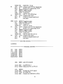
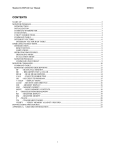
TABLE OF CONTENTS
ACKNOWLEDGEMENTS
ii
ABSTRACT
vi
LIST OF TABLES
vii
LIST OF FIGURES
viii
CHAPTER
1. INTRODUCTION
1
1.1 Introduction
1
1.2 Diagnostic Tool
2
1.3 Overview of the Problem
4
2. SPECIFICATIONS
6
2.1 Introduction
6
2.2 Network Architecture Support
6
2.3 Network Elements and Structure
7
2.4 Modulation
8
2.5 Protocol /Interface
9
2.6 Timing Requirements for Pulse Width Modulation
11
2.6.1
The One " 1 " and zero "0" Bits
13
2.6.2
Start of Frame (SOF)
14
2.6.3
End of Data (EOD)
14
2.6.4
End of Frame (EOF)
15
2.6.5
Inner-Frame Separation (IFS)
15
2.6.6
Break (BRK)
15
2.6.7
Idle Bus (Idle)
16
2.7 Timing Requirement for Variable Pulse Width Modulation
16
2.7.1
The one " 1 " and zero "0" Bits
18
2.7.2
Start of Frame (SOF)
18
2.7.3
End of Data (EOF)
18
in
2.7.4
EndofFrame(EOF)
18
2.7.5
Inter-Frame Separation(IFS)
18
2.7.6
Break(BRK)
18
2.8 Electrical Criteria
19
2.8.1
Overall Electrical/Electromagnetic criterion
19
2.8.2
Electromagnetic Compatibility (EMC)
19
2.9 Connector
20
AN OVERVIEW OF THE 68HC12
21
3.1 Introduction
21
3.1.1
Features of 68HC12B32
21
3.1.2
Single Chip Operation
23
3.1.3
Expanded Mode Operation
23
3.1.4
Programming Hardware
24
3.1.5
Instruction Set
25
3.1.6
The Timer Module
25
3.1.7
Analog to Digital Converter
26
3.1.8
Communications
26
3.1.9
I/O Pins Galore
26
3.2 MC68HC12U-Controller Based Evaluation
27
3.2.1
Hardware
29
3.2.2
The Hardware Configuration of the 68HC12
30
3.2.3
Firmware
33
3.3 Standard 68HC12 Timer Module
33
3.3.1
The Big picture
34
3.3.2
The Timer System Control Registers
36
3.3.3
The Timer Counter Register
36
3.3.4
The Timer Control Registers
38
DESIGN SOLUTION
40
4.1 Approach and Implementation
40
IV
4.2 Firmware Algorithm
41
4.3 Software
44
4.4 Diagnostic Message Format
48
4.5 Transceiver Circuit
49
5. RESULTS
52
5.1 Bit Modulator and PRT_FIND Module Verification
52
5.2 SOF, EOD, EOF Detectors Verification
61
5.3 BRK Detector Verification
65
6. CONCLUSIONS
68
REFERENCES
71
APPENDIX
72
ABSTRACT
This project deals with developing a system, which can be implemented by Texas
Department of Transportation, as a part to develop a PC based universal scan tool, which
can later be used to create a database on the different tests and use for future research. A
microprocessor based physical layer for OBD II test equipment that can be used to test
any car that supports the ON-Board Diagnostics II protocol has been developed. This acts
as the interface tool between the OBD II system on the vehicle and the application layer
residing on the PC. The verification of the system has been done, by generating sample
data that matches real time data. Conclusions and suggestions for future work are
discussed.
VI
LIST OF TABLES
2.1 PWM Pulse width times
13
2.2 VPWM pulse width times
17
3.1 MC68HC12B32 Port description summary
27
3.2 Prescalar value selection table
38
3.3 Edge detector circuit configuration
39
4.1 Diagnostic message format
48
Vll
LIST OF FIGURES
2.1 ' VBit definition
11
2.2'0'Bit definition
11
2.3 PWM Frame Symbols
12
2.4 PWM Break
12
2.5 VPW One and Zero Bit definition
16
2.6 VPWM Frame Symbols
17
3.1 Evaluation Board of MC68HC12
28
3.2 Block diagram of Evaluation Board
29
3.3 Block diagram of MC68HC12BC32
31
3.4 Standard Timer block diagram
35
3.5 Timer System Control Register
36
3.6 Timer Counter Register
37
3.7 Timer Control Register 3
39
3.8 Timer Control Register 4
39
4.1 Block diagram of Embedded U-processor system for the Physical layer
41
4.2 Flow chart of Main module, for MC68HC12 microcontroller
43
4.3 Flow chart of PROTOCOL FIND module for MC68HC12 microcontroller
45
4.4 Flow chart showing control flow in detector modules
47
4.5 Block diagram of the Transceiver Circuit
50
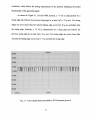
5.15 byte sample data transmitted by PWM transmit protocol
53
5.2 First byte ($68) of the PWM sample data
54
5.3 Second byte ($6A) of the PWM sample data
55
Vlll
5.4 Third byte ($F1) of the PWM sample data
55
5.5 Mode byte ($01) of the PWM sample data
56
5.6 PID byte ($00) of the PWM sample data
56
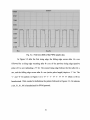
5.7 5 byte sample data transmitted by VPWM transmit protocol
57
5.8 First byte ($61) of the VPWM sample data
58
5.9 Second byte ($6A)ofthe VPWM sample data
59
5.10 Third byte ($F1) of the VPWM sample data
59
5.11 Mode byte ($01) of the VPWM sample data
60
5.12 PID byte ($00) of the VPWM sample data
60
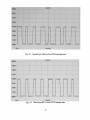
5.13 SOF and EOD marks for VPWM
61
5.14 EOF after 2 sample frames for VPWM
62
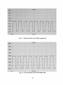
5.15 EOF after 2 sample frames for PWM
64
5.16 SOF, EOD, EOF, BRK marks for VPWM
66
5.17 Two Frames and a BRK symbol for PWM
67
IX
CHAPTER 1
INTRODUCTION
1.1. Introduction
As the quality of air is decreasing in urban areas, state and national regulatory
agencies are passing more stringent automobile emission standards. California is the first
state to take serious action with regard to automobile emissions. The California Code of
Regulations (CCR) has developed an enhanced inspection and maintenance (I&M)
program that was to be implemented in the year 1996. All 1996 and later model year cars
light and medium-duty trucks sold in California have to be equipped with an OBD (On
Board Diagnostic) system.
On Board Diagnostic (OBD) systems introduced by the 'California Air Resources
Board' are incorporated into the computers on-board new vehicles to monitor
components and systems that may affect emissions when malfunctioning. The second
generation of OBD requirements, which is known as OBD II, has been fully in effect
since the 1996 model year for Passenger Cars, Light Duty Trucks, and Medium Duty
Vehicles With Feedback Control Systems. Section 1968.1 of Title 13 of the California
Code of Regulations (CCR) defines the diagnostic functions to be supported by vehicles
and also defines functions to be supported by test equipment that interfaces with the
vehicle diagnostic functions.
The OBD-II regulations define diagnostic functions to be supported by the vehicle
and functions to be supported by the test equipment that interfaces with the vehicle
diagnostic functions. Ranges of test equipment can vary from a handheld scan tool, to a
PC based diagnostic computer to perform the required interface support function.
1.2. Diagnostic Tool
The OBD II systems monitor virtually every component that can affect the
emission performance of a vehicle. If a problem is detected, the OBD II system
illuminates a warning lamp on the vehicle instrument panel to alert the driver. This
warning lamp typically contains the phrase Check Engine or Service Engine Soon. The
system will also store important information about a detected malfunction so that a repair
technician can accurately find the problem with an OBD II Scan Tool and fix the problem
accordingly.
According to the OSI (open system architecture) model a system such as Scan
Tool is comprised of three layers-User Interface, Data Link Layer, and Physical Layer.
At the top of the OSI reference model is the Application (User Interface) Layer.
This layer establishes the relationship between various application input and
output devices, including what is expected of human operators. This layer documents the
high level description of the function including control algorithms if appropriate. An
example of an Application Layer functional description might be: "Pressing the lead lamp
button shall cause the low beam head lamp, marker and tail lamp filaments to be
energized." Legislated diagnostics is another area in which application layer requirements
need to be specified.
The primary function of the Data Link Layer is to convert bits and/or symbols to
validated error free frames/data transmission. Typical services provided are serialization
(parallel to serial conversion) and clock recovery or bit synchronization. An important
additional service provided by the Data Link Layer is error checking. When errors are
detected, they may be corrected or higher layers may be notified.
The Physical Layer and its associated wiring form the interconnecting path for
information transfer between Data Link Layers. Typical Layer protocol elements include
voltage/current levels, media impedance, and bit/symbol definition and indication of
different frame timings.
An OBD II Scan Tool can be used to perform the required interface support
functions. The basic functions, which the OBD II Scan Tool is required to support or
provide, are:
•
Automatic hands off determination of the communication interface used;
•
Obtaining and displaying the status and results of vehicle on board diagnostic
evaluations;
•
Obtaining and displaying OBD II emission related diagnostic trouble codes as
defined in SAE J2012 JUL96;
•
Obtaining and displaying OBD II emission related current data;
•
Obtaining and displaying OBD II emissions related freeze frame data;
•
Clearing the storage of OBD II emissions related diagnostic trouble codes;
•
Obtaining and displaying OBD II emissions related test parameters and results
as described in SAE J1979;
•
Provide user manual/or help facility.
The OBD II scan tool must be able to communicate with the vehicle control
modules using the prescribed communication interfaces. There are three protocols that
are currently proposed. The interfaces are: (1) SAE J1850 41.6 Kbps PWM, (2) SAE
J1850 10.4 Kbps VPWM and (3) ISO 9141-2. Here only two protocols SAE J1850 41.6
Kbps PWM, and SAE J1850 10.4 Kbps VPWM have been implemented.
1.3. Overview of the Problem
Before the introduction of Universal OBD II Scan Tool system various
Automobile manufacturers came up with their own Scan Tools. This lead to expensive
investment on the part of automobile servicing companies for procuring various scan
tools made by various manufacturers for various automobiles. To eliminate the lack of
generality, the utilization of a PC to interface with the vehicle is desirable. Accordingly
the PC must be able to diagnosis the data, store the acquired data from a variety of
vehicles, and maintain a database for future research. It should also be able to analyze the
data to check the functionality of the vehicle and finally, the PC-based scan tool must be
compatible for future developments in this area. To achieve these functions a
microprocessor-based prototype has been recommended, which can be directly hooked
up to a standard PC.
The Texas Department of Transportation launched this project, recommending a
PC based Universal Scan Tool design, which can later be used to create a database on the
different tests and use for future research. The 'Data Link', 'Application' and 'Physical'
layers of a universal OBD II scan tool have been designed by Miss Sunitha Godavarthy
[4], Mr. Geng Fu [5], and Mr. Sohail Saarwar [6], as part of this project.
This project deals with the design of the Physical layer of an OBD II test
equipment, that can be used to test any car that supports the On Board Diagnostics II
protocol. An attempt has been made to design the Physical layer which acts as the
interface tool between the OBD II system on the vehicle and the application layer
residing on the PC. The objective is to simplify and increase the versatility of the system
using a microprocessor-based system as the physical layer.
The scope of this thesis is to contribute to the setting of specifications, thereon to
the designing of the prototype of the Physical Layer of a Universal (generic) OBD II
Scan Tool by writing assembly code to obtain specified functionality. A microprocessor
was used as a Physical Layer of OBD II Scan Tool, and which can be directly hooked up
to a standard PC. This would provide the independent service industry with a low cost
piece of equipment that is useful with any OBD II equipped vehicle.
The second chapter explains the network architecture and the timing requirements
for the different modulations. In the third chapter, the author gives an overview of
MC68HC12, stressing on the standard timer module of the chip. The fourth chapter deals
with the approach to the problem, assembly code solution and effectiveness of the source
code functioning as the physical layer. Results are described in Chapter 5. Conclusions
and future improvements are suggested in Chapter 6.
CHAPTER 2
SPECIFICATIONS
2.1 Introduction
Specifications for the Physical Layer of an OBD II Scan Tool include Network
Architecture Support, Network elements, Modulation, Protocol/Interface support, Timing
requirements for the protocol supported, Electrical/Electromagnetic criteria, and
Connector Type. These individual specifications are discussed below.
2.2 Network Architecture Support
It is the intent of the OBD II network to interconnect different electric modules on
the vehicle using an "Open Architecture" approach. An open architecture network is one
in which the addition or deletion of one or more modules (data nodes) has minimal
hardware and/or software impact on the remaining modules. In order to support an open
architecture approach, the Class B Network, which is a system whereby data is
transferred between nodes to eliminate redundant sensors and other system elements,
utilizes the concept of Carrier Sense Multiple Access (CSMA) with non-destructive
contention resolution. Additionally this network supports the prioritization of frames such
that, in the case of contention, the higher priority frames will always win arbitration and
be completed.
From a topology point of view a 'single-level bus topology', the simplest
topology, is currently being used in several automotive applications. In a single-level bus
topology, the same data bus interconnects all nodes. The redundancy requirements of a
particular application may require a single-level topology to be implemented using
multiple interconnecting cables operating in various modes (active or passive). However,
the requirement to use multiple buses for redundancy purposes does not change the
single-level bus topology definition if the following criteria are maintained:
a. All nodes/devices transmit and receive from a single path;
b. All nodes/devices receive all frames at the same time;
c. Communication on each data bus is identical.
Although various methods of data bus control can be used, this Class B network is
intended for "masterless" bus control. The principal advantage of the masterless bus
control concept is its ability to provide the basis for an open-architecture data
communications system. Since a master does not exist, each node has an equal
opportunity to initiate data transmission once an idle bus has been detected. However, not
all nodes and/or data are of equal importance. Prioritization of frames is allowed and the
highest priority frame will always be completed. This also implies that frame/data
contention will not result in lost data. Two disadvantages of the masterless bus concept
are that the data latency cannot be guaranteed, except for the single highest system
priority frame, and bus utilization extremes are difficult to evaluate.
2.3 Network Elements and Structure
The general format of a message frame, which is transmitted over the OBD II
Bus, consists of different Network Elements: Idle, SOF, DATA, EOD, CRC, NB, IFR,
EOF, IFS, BRK.
The preceding acronyms are defined as follows:
Idle:
Idle Bus that occurs before SOF and after IFS;
SOF : The SOF (Start of Frame) mark is used to uniquely identify the start of a
frame.
DATA: Data bytes each 8 bits long.
EOD: End of Data (EOD only when IFR is used) is used to signal the end of
transmission by the originator of a frame.
CRC : Cyclic Redundancy Check Error Detection Byte.
NB: Normalization bit is applicable to 10.4Kbps implementation. The NB defines
the start of the in-frame response.
IFR: The in-frame response bytes are transmitted by the responders after the
EOD.
EOF : The EOF (End of Frame) defines the end of frame.
IFS: The IFS (Inter-Frame separation) is used to allow proper synchronization of
various nodes during back-to-back frame transmissions. A transmitter must not
initiate transmission on the bus before the completion of the IFS minimum period.
BRK: This BRK (Break) can occur any time on a network.
2.4 Modulation
A given OBD II system is required to use one of two types of modulation, Pulse
Width Modulation (PWM) or Voltage Pulse Width Modulation (VPWM). PWM is a data
format where the width of a pulse of constant voltage or current determines the value
(typically one or zero) of the data transmitted. VPWM is a method of using both the state
of the bus and the width of the pulse to encode bit information. This encoding technique
is used to reduce the number of bus transitions for a given bit rate. One embodiment
would define a "ONE" (1) as a short active pulse or a long passive pulse while a "ZERO"
(0) would be defined as a long active pulse or a short passive pulse. Since a frame is
comprised of a random l's and 0's, general byte or frame times cannot predicted in
advance. The timing requirements for different network elements for both PWM and
VPWM are given later in the chapter.
2.5 Protocol/Interface
There are three types of communication interfaces that are supported by the OBD
II standard. These standards are specified in SAE J1850 PWM (41.6 Kbps), SAE J1850
VPW (10.4Kbps), and ISO 9141-2, and only one of these is allowed to be used in any one
vehicle to access all supported OBD II functions.
When connected to a vehicle the OBD II Scan Tool must automatically attempt to
determine which of the possible communication interfaces is being used in the vehicle to
support OBD II related functions. The tool must continue to try to determine which
interface is being used until it is successful in doing so. No user input can be required,
nor allowed, to determine the appropriate interface.
Indications or messages must be displayed during this process informing the user
that initialization is taking place and, if all interface types have been tested and none is
responding properly to the request for OBD II services, the OBD II Scan Tool must
indicate the user:
a. To verify that the ignition is on.
b. To check the Emissions label or vehicle service information to verify that the
vehicle is OBD II equipped.
c. To check that the tool is properly connected to the vehicle.
If all the above three conditions are satisfied then it should indicate that there is a DATA
link failure.
Only the following steps may be used by an OBD II Scan Tool to attempt to
determine the type of communications interface used in a given vehicle to support OBD
II functions.
a. Test for SAE J 1850 41.6 Kbps PWM:
•
Step 1 - Enable the SAE J1850 41.6 Kpbs PWM interface
•
Step 2 - Send a mode 1 PID 0 request message
•
Step 3 - If a mode 1 PID 0 response message is received then SAE J1850 41.6 Kbps
PWM is the type of interface used in a vehicle for OBD II support.
b. Test for SAE j 1850 10.4 Kbps VPWM:
•
Step 1 - Enable the SAE Jl 850 10.4 Kbps VPW interface
•
Step 2 - Send a mode 1 PID 0 request message
•
Step 3 - If a mode 1 PID 0 response message is received then SAE J1850 10.4 Kbps
VPWM is the type of interface used in a vehicle for OBD II support.
The previous tests may be performed in any order and where possibly be
performed in parallel. The mode 1 PID 0 request and response messages are defined in
SAE J1979. SAE J1850 defines the requirements of SAE J1850 interfaces.
The timing requirement for SAE J1850 41.6Kbps (PWM) and SAE J1850
10.4Kbps (VPW) interfaces can be found respectively in Tables 3 and 5 of section 7.3.2.
10
in the document "SAE J1850 JUL95 - CLASS B Data Communications Network
Interface" in the chapter 2.2 in the book SAE On-Board Diagnostics for Light and
Medium Duty Vehicles Standards Manual (1997 Edition) published by Society of
Automotive Engineers.
2.6 Timing Requirements for Pulse Width Modulation
The nominal timing requirements for PWM bits and symbols are shown below
(Figures 2.1-2.4). Detail timing is given in Table 2.1.
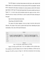
[>
TP3
^
Previous Bit
o r Ivdark
4 " ^ r p ^-*\
*^,
'
**j>» 3 ^ ,
Fig. 2.1: " 1 " Bit Definition
-Tp3
-4-
P Pr re ev vi ioo uu ss B i t
^
o r Ivtarlc
Tp2
_r
fc-i^ fc-i^
'
"O"
-j--Tpl
Bit
Fig. 2.2: "0" Bit Definition
11
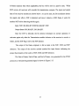
1—~|
_T
4
4
4
4
4
P6
P5"
-IP4
.EOD
.SOF
.EOF
.IFS
Fig. 2.3: PWM Frame SYMBOLS
L-
_Tp4_
TpS-BRK-
Fig. 2.4: PWM Break (BRK)
12
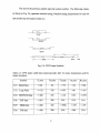
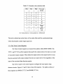
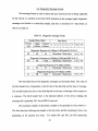
Table 2.1: PWM pulse width times (microseconds); here Tx means transmission and Rx
means reception.
Symbol
Tx,min Tx,nom
Tx,max
Rx,min
Rx,max
Tpl: Active phase " 1 "
>=7
8
<=9
>=6
<=11
Tp2: Active phase "0"
>=15
16
<=17
>=14
<=19
Tp3: Bit time
>=23
24
<=25.5
>=22
<=27
Tp4: SOF/EODtime
>=47
48
<=51
>=46
<=63
Tp5: EOF time
>=70
72
<=76.5
>=70
<=N/A
Tp6: IFS time
>=94
96
N/A
N/A
N/A
Tp7: Active SOF
>=30
32
<=33
>=30
<=35
Tp8: Active BRK
>=38
40
<=41
>=38
<=43
Tp9: BRK to IFS time
>=118
120
N/A
N/A
N/A
TplO: SOF to Data rising edge
>=47
48
<=51
>=45
<=52
TP11: Passive to next rising edge
>=6
N/A
N/A
>=4
N/A
The symbol timing reference for PWM encoding is based on the transitions from the
passive to active state. The SOF and each data bit in PWM has a leading edge from which
all subsequent timing is derived.
2.6.1. The One " 1 " and zero "0" Bits
A " 1 " bit is characterized by a rising edge that follows the previous rising edge by
at least Tp3. Two rising edges shall never be closer than Tp3. The falling edge occurs
Tpl after the rising edge, as shown in Figure 2.1.
13
A "0" bit is characterized by a rising edge that follows the previous rising edge by at
least Tp3. Two rising edges shall never be closer than Tp3. The falling edge occurs Tp2
after the rising edge, as shown in Figure 2.2. A next data bit rising edge occurs Tl 1 after
the previous falling edge (if applicable).
2.6.2 Start of Frame (SOF)
The Start of Frame (SOF) mark has the distinct purpose of uniquely determining
the start of a frame, as shown in Fig. 2.3. The SOF is characterized by:
a. A reference rising edge that follows the previous rising edge by at least Tp5.
b. A falling edge that occurs T7 after the reference rising edge.
c. The rising edge of the first data bit will occur at Tpl 0 after the reference rising
edge.
2.6.3 End of Data (EOD)
End of Data is used to signal the end of transmission by the originator of a frame.
The In-Frame Response (IFR) section of the frame begins immediately after the EOD bit
as shown in Figure 2.3. If the In-Frame Response feature is not used, then the bus would
remain in the passive state for an addition bit time, thereby signifying an End of Frame
(EOF).
For In-Frame Response, the response byte(s) are divided by the responders and
begin with the rising edge-of the first bit of the response, Tp4 after the rising edge of the
bit sent from the originator of the frame.
14
If the first bit of the response byte does not occur at Tp4, and the bus remains
passive for one additional bit time (total time Tp5) then the originator and all receivers
must consider the frame complete (i.e., EOD has been transformed into an EOF).
2.6.4 End of Frame (EOF)
The completion of the EOF defines the end of a frame (by definition, an EOD
forms the first part of the EOF, as shown in Fig. 2.3. After the transmission byte
(including in-frame response byte where applicable), the bus will be left in a passive
state. When EOF has expired (Tp5 after the rising edge of the last bit), all receivers will
consider the transmission compete.
2.6.5 Inner Frame Separation (IFS)
Inner-Frame Separation allows proper synchronization of various nodes during
back-to-back frame operation, as shown in Figure 2.3. A transmitter that desires bus
access must wait for either of two conditions before transmitting a SOF:
a. IFS minimum has expired. (Tp6 after the rising edge of the last bit).
b. EOF minimum and another rising edge has been detected.
(Tp5 after the
rising edge of the last bit).
2.6.6. Break (BRK)
BRK is allowed to accommodate those situations in which bus communication is
to be terminated and all nodes reset to a " ready-to-receive" state, as shown in Fig. 2.4.
The PWM Beak symbol is an extended SOF symbol and will be detected as an
15
'individual" symbol to some devices, which will then ignore the current frame, if any.
Following the break symbol, an IFS following BRK (Tp9 after the rising edge of the
break) is needed to synchronize the receivers. If the " Breaking" device wishes to obtain
guaranteed access to the bus, the highest priority frame must be sent, otherwise, other
frames may gain access under the normal rules of arbitration.
2.6.7 Idle Bus (Idle^
Idle bus is defined as any period of passive Bus State occurring after an IFS
minimum. A node may begin transmission at any time during an idle bus. During an idle
bus, any node may transmit immediately. Contention may still occur when two or more
nodes transmit nearly simultaneously; therefore, synchronization to rising edges must
continue to occur.
2.7. Timing Requirement for Variable Pulse Width Modulation
The SOF symbol, "0" bit, and " 1 " bit are defined by the time between two
consecutive transmission and the level of the bus, active or passive, as shown in Fig. 2.5.
The EOD, EOF, IFS, and Break symbols are defined simply by the amount of time that
has expired since the last transition. EOD, EOF, and IFS are all passive symbols and the
Break is an active symbol.
Therefore, there is one symbol per transition and one
transition per symbol.
-
T-v2
—
" 1"
J-
Tr v
v 2
2
Bit
-Tvl
•. '—
»-
Fig. 2.5: VPW One and Zero Bit Definition
16
The end of the previous symbol starts the current symbol. The following values,
as shown in Fig. 2.6, represent nominal timing. Detailed timing requirements for each bit
and symbol can be found in Table 2.2.
-Tv3"SOF"
-Tv3—
'EOD"
Tv4'EOF"
Tv6Tv4-
"Tv5
-BRK-
EOF
IFS
Fig. 2.6: VPW Frame Symbols
Table 2.2: VPW pulse width times (microseconds); here Tx means transmission and Rx
means reception.
Symbol
Tx,min
Tx,nom
Tx,max
Rx,min
Rx,max
Tvl: Short Pulse
>=49
64
<=79
>34
<=96
Tv2: Long Pulse
>=112
128
<=145
>96
<=163
Tv3: SOF/EODtime
>=182
200
<=218
>163
<=239
Tv4:
EOF time
>=261
280
N/A
>239
N/A
Tv5:
BRK time
>=280
300
<=5000
>=239
<=10°
Tv6:
IFS time
>=280
300
N/A
>280
N/A
17
2.7.1. The one " 1 " and zero "0" Bits
A " 1 " bit is either a Tv2 passive pulse or a Tvl active pulse. Conversely, a "0"
bit is either a Tvl passive pulse or a Tv2 active pulse, as shown in Fig. 2.5.
2.7.2. Start Of Frame (SOF)
SOF is an active pulse, Tv3 in duration, as shown in Fig. 2.6.
2.7.3. End Of Data (EOD)
EOD is a passive pulse, Tv3 in duration, as shown in Fig. 2.6.
2.7.4. End Of Frame (EOF)
EOF is a passive pulse, Tv4 in duration, as shown in Fig. 2.6.
2.7.5. Inter-Frame Separation (IFS)
Inter-Frame Separation is used to allow proper synchronization of various nodes
during back-to-back frame operation. A transmitter that desires bus access must wait for
either of two conditions before transmitting a SOF, as shown in Fig. 2.6:
a.
IFS minimum has expired (Tv6).
b.
EOF minimum and another rising edge has been detected (Tv4).
2.7.6. Break (BRK)
BRK is allowed to accommodate those situations in which bus communication is
to be terminated and all nodes reset to a "ready-to receive" state (see Fig. 2.6). The VPW
Break symbol will be detected as an "Invalid" symbol to some devices, which will then
18
ignore the current frame, if any. The VPW Break symbol is a long active period (Tv5).
Following the break symbol, an IFS period (Tv6) is needed to synchronize the receivers
and the normal IFS rules for transmitting a SOF during back-to-back operation apply. If
the " Breaking" device wishes to obtain guaranteed access to the bus, the highest priority
frame must then be sent, otherwise, other frames may gain access under the normal rules
of arbitration.
2.8. Electrical Criteria
The DC parameter requirements for SAE J1850 41.6Kbps (PWM) and SAE J1850
10.4Kbps (VPW) interfaces can be found respectively in Tables 4 and 6 of section 7.3.2.
in the document "SAE J1850 JUL95 - CLASS B Data Communications Network
Interface" in the chapter 2.2 in the book SAE On-Board Diagnostics for Light and
Medium Duty Vehicles Standards Manual (1997 Edition) published by Society of
Automotive Engineers.
2.8.1. Overall Electrical / Electromagnetic criterion
According to the specifications of overall electrical criterion, an OBD II Scan
Tool must operate normally within a range of 8.0 to 18.0 V D.C, survive a steady-state
voltage of up to 24.0 V D.C. for at least 10.0 min., and must not draw more than 4.0 A at
14.4 V D.C.
2.8.2. Electromagnetic Compatibility (EMC)
According to the specifications of overall electromagnetic criterion, an OBD II
Scan Tool must not interfere with the normal operation of vehicle modules. The normal
19
operation of the tool must be immune to conducted and radiated emissions present in a
service environment and when connected to a vehicle. It is also required that the tool
must be immune to reasonable levels of Electrostatic Discharge (ESD). EMC and ESD
measurements and limits will be according to SAE Jl 113.
2.9. Connector
The OBD II Scan Tool Connector has to be designed according to specifications
in articles 4 and 5 of chapter 2.1 (document "SAE J1962 JAN95 - Diagnostic
Connector") in the book SAE On-Board Diagnostics for Light and Medium Duty Vehicles
Standards Manual (1997 Edition) published by Society of Automotive Engineers.
20
CHAPTER 3
AN OVERVIEW OF THE 68HC12
3.1 Introduction
A big leap in enhancement of processors is the development of Motorola's
68HC12. Some of the great features of the HC11 have been taken, improved, and put
atop a new CPU core to form HC12. The MC68HC12 micro controller unit is a 16-bit
central processing unit. It has a 32 Kbyte flash EEPROM, 1-Kbyte RAM, 768-byte
EEPROM, 8-channel timer, 16-bit pulse accumulator, a 8-bit analog-to-digital converter.
The core runs on a faster crystal (currently 16Mhz) and runs most instructions faster
because of the internal clock (8Mhz), plus it runs many instructions in only one clock.
The 6HC12 chip is much more complex than the HC11 but flexible and allows much
more efficient use of ROM space.
CPU 12 has full 16-bit data paths, and can perform arithmetic operation up to 20
bits wide for high-speed math execution. It also allows instructions with odd byte counts,
including many single-byte instructions.
3.1.1 Features of 68HC12B32
Some of the features of the 68HC12B32 are given below:
•
Low-Power, High-Speed M68HC12 CPU;
i. Upward compatible with 68HC11 instruction set,
ii. 20-bit ALU,
iii. Enhanced indexed addressing,
iv. Instruction Queue buffering,
21
Power Saving STOP and WAIT Modes;
Memory;
i.
1024 Bytes RAM with Single Cycle access for aligned or misaligned
read/write,
ii. 32K Bytes FLASH Electrically Erasable Programmable Read-Only
Memory (EEPROM),
Single-Wire Background Debug Mode;
Non-Multiplexed Address and Data Buses;
Seven Programmable Chip Selects with Clock Stretching (Expanded Modes);
8-Channel, Enhanced 16-Bit Timer with Programmable Prescaler;
i. All Channels Configurable as Input Capture or Output Compare,
ii. Flexible Choice of Clock Source,
iii. Simple PWM mode,
16-Bit Pulse Accumulator;
Real-Time Interrupt Circuit;
Computer Operating Properly (COP) Watchdog, Clock Monitor, and periodic
Interrupt Timer;
Two Enhanced Asynchronous Non-Return to Zero (NRZ) Serial Communication
Interfaces (SCI);
Enhanced Synchronous Serial Peripheral Interface (SPI);
8-Channel, 8-Bit Analog-to-Digital Converter (ATD);
Pulse width Modulator;
i. 8-Bit, 4-Channel or 16-Bit, 2-Channel,
ii. Programmable center aligned and Left aligned output,
5-bit, 9-bit, or 16-bit signed constant offsets and 16-bit offset indexed direct and
accumulator D offset indexed-indirect addressing;
Available in 80-Pin Quad Flat Pack (QFP) Packaging.
22
3.1.2 Single Chip Operation
One of the truly great features of the HC12 is its ability to run in a single chip
configuration. This makes for an extremely compact design, which uses less power. It
also gives the 68HC12 lots of I/O pins.
In single chip version, the 1024 bytes of RAM and 4096 bytes of EEPROM are
worth their weight in gold. With 1024 bytes, twice what the HC11 provided, we can do
some better programming and processing. There are no external address and data buses in
this mode. All pins of Ports A, B and E are configured as general purpose I/O pins.
The 4k of EEPROM, compared to 2k on the HC11 is a bit of an under statement.
The CPU 12 instructions are encoded differently than the HC11. This allows them to pack
more functionality into the instructions. Indexed instructions, for example, require less
memory since they are encoded into the instruction byte. Motorola has tested the relative
size of M68HC11 and CPU 12 code. By rewriting several smaller assembly programs
from scratch the CPU 12 code is typically about 30% smaller. These savings are mostly
due to improved indexed addressing. It is useful to compare the relative sizes of C
programs. A C program compiled for the CPU 12 is about 30% smaller than the same
program compiled for the M68HC11. The difference is largely attributable to better
indexing. The 68HC12B32 also supports 32K of FLASH memory along with the Ik of
RAM.
3.1.3 Expanded Mode Operation
The 68HC12 can run in an expanded mode. This allows you to connect external
memory and other peripherals to the chip, at the expense of ports A and B (16 lines of
23
I/O). The external address space is 64k long.
The 68HC12 has a very powerful external memory interface. There are Address
lines A0-A21 and data lines D0-D15. Through a rather rich and complex set of options,
we can choose to have up to about 5MB of memory with a 16-bit wide data bus. It does
this with built in bank switching hardware and support for bank switching in some of the
instructions.
To reduce hardware requirements we can optionally have a 8 bit data path if we
so desire. The chip is very flexible with respect to the memory interface. The subject of
expanded memory on the 68HC12 gets complicated, with a lot of addressing modes,
which are to be studied closely.
3.1.4 Programming Hardware
The 68HC11 has a special mode called bootstrap mode which allows you to
download code via the serial port. It requires only a serial port on your PC and a free
program to download.
The 68HC12 does NOT have this feature. It does, however, have a special serial
interface that allows you to read/write memory. This is called the Background Debug
mode, which has a single wire interface. This is going to require some special
programming hardware. The Background Debug Mode is a special CPU 12 operating
mode that is used for system development and debugging. Executing BGND when BDM
is enabled puts the CPU 12 in this mode. Some activities such as reading and writing
memory locations can be performed while the CPU is executing normal code with no
effect on real time system activity.
24
3.1.5 Instruction Set
The instruction set of the 68HC12 is pretty decent and is easy to learn. It is a
super set of the 68HC11-instruction set. The 68HC12 is 'source code compatible' with the
68HC11. This means that the instruction set is the same or the assembler will
automatically convert things. The CPU 12 provides expanded functionality and increased
code efficiency.
Source code compatible means that you should be able to take the assembler files
for the 68HC11 and compile them with the asl2.exe, and it should work. The binary
images are very different, however. So, the binary images from a 68HC11 cannot be on a
68HC12.
In a 68HC12, the same instruction set can be used to access memory, I/O, and
control registers. There are instructions for signed and unsigned arithmetic, division and
multiplication with 8-bit, 16-bit and some larger operations, which makes the 68HC12
worthwhile to use for real time applications. Additional instructions, which can handle
memory to memory moves, can also come in handy.
3.1.6 The Timer Module
On the 68HC12, the timer section has really been beefed up. The standard timer
module consists of a 16-bit programmable counter driven by a prescaler. It contains eight
complete 16-bit input capture/output compare channels and one 16-bit pulse accumulator.
The pulse accumulator is also available by giving up one of the TOC channels. The
Timer module is explained in detail later in the section 3.4.
25
3.1.7 Analog to Digital Converter
The A/D converter built into the 68HC12 has been one of the most popular
features that keeps it the forefront in many real time applications. The 8 channels are
available on PORTE, and can be sampled 4 at a time.
The A/D converter on the 68HC12 provides result registers for all 8 values. This
means that all 8 values can be sampled without doing bank switching. To keep
compatibility with existing code, it appears that 4 channel multiplexing works as well.
3.1.8 Communications
The 68HC12 has two independent serial I/O sub systems. The SCI Serial
communication interface and the SPI Serial Peripheral interface. Each serial pin shares
function with the general-purpose port pins of port S. The SCI subsystem has a single
wire operation mode, which allows the unused pin to be available as general purpose I/O.
The SPI subsystem is compatible with the 68HC11 SPI, with additional features of SS
output and bi-directional output. It is also capable of running much faster (4 MBit/S).
The onboard UARTs are independently clocked, and can be driven at standard
speeds up to 38400, which is a big leap and helps to drive the serial port faster.
3.1.9 I/O Pins Galore
The 68HC12 has all Port A, Port B and Port E for a 24 pins of I/O that a 68HC11
has, plus Port DLC, Port AD, Port P, Port T and finally Port S. Table 3.1 below shows
the port assignments, which shows that, there are a lot of I/O pins (64 pins!).
26
Table 3.1 MC68HC12B32 Port description summary
Port
Type of
Description
Port
A
General-purpose I/O in single-chip modes. External address bus ADDR[15:8] in
In/Out
expanded modes.
B
General-purpose I/O in single-chip modes. External address bus ADDR[7:0] in
In/Out
expanded modes.
Has 7 General-purpose I/O pins, PDLC [6:0]. Register DDRDLC determines whether
DLC
In/Out
each port DLC pin is an input or output.
E
In/Out
Mode selection, bus control signals and interrupt service request signals; or generalpurpose I/O.
The four pulse width modulation channel outputs share general-purpose port P pins.
The PWM function is enabled with PWEN register. When PWM mode is not in use the
P
out
port pins may be used as general purpose I/O.
Serial communications interface and serial peripheral interface subsystems and
S
In/Out
general-purpose I/O.
T
In/Out
Timer system and general-purpose I/O.
Analog-to-digital converter and general-purpose input. When analog- to-digital
AD
In
functions are not enabled can be used as general Input pins, PAD [7:0].
3.2 MC68HC12 U-Controller based evaluation board
The embedded microprocessor system being designed for the physical layer of the
Universal OBD II Scan Tool uses the M68HC12 micro-controller based Evaluation
Board Unit (EVBU). MC68HC12 micro-controller is chosen for its architectural
simplicity, low cost, and wide availability. The EVBU is an economical tool for
debugging and evaluating the operation of MC68HC12 MCU. By providing the essential
27
MCU timing and I/O circuitry, the EVB simplifies user evaluation of prototype hardware
and software.
User code can be assembled in one of two methods. For small programs or
subroutines, D-bugl2's single line assembler/disassembler may be used to place object
code directly into the EVB's RAM or EEPROM. The second method, generally used for
larger programs, is by using Motorola's MCU assembler on a host computer to generate
an S-record object file. This file then can be downloaded into EVB's memory using DBugl2's 'load' command. The monitor program is then used to debug the assembled user
code. Overall debugging/evaluation control of the EVBU is provided via terminal
interaction by the monitor program. RS232C terminal I/O port interface circuitry
provides communication and data transfer operations between the EVBU and external
terminal/host computer devices. A fixed baud rate of 9600 is provided for the terminal
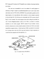
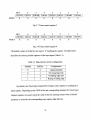
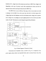
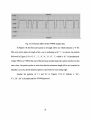
I/O. The figure below shows the EVB's layout and locations of major components, as
viewed from the component side of the board (Fig. 3.1).
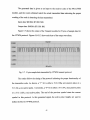
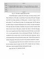
PROTOTYPE AREA
UCQBHC919B3SMCU
BACKGROUND DEBUQ
MODE OUT
BACKGROUND DEBUG
MODE IH
VPP MHJT
POWER
CONNECTOR
Fig. 3.1 Evaluation board of MC68HC12
28
As shown in the figure above the EVB board is a double-sided PCB, which
provides the platform for interface and power connections to MC68HC12 MCU chip.
Here, in this design, the basic function of the EVBU is to get a message from the PC and
then, using the external hardware, to send a frame following the timing constraints of the
OBD II bus. In the same way, while receiving frames from the OBD II bus it collects data
coming from the decoder circuit then decodes the frame and stores it temporarily and
eventually sends the frame to the PC, where the data link layer can access the frame.
Actually the EVBU is comprised of two sub-modules; one is the hardware and
the other one is the firmware. These sub-modules are discussed below:
3.2.1 Hardware
EVBU contains a 68HC12 micro-controller, a timer IC (the MC68HC68T1), and
WIRE-WRAP AREA
PXD/PDO
PAO-PA7
TXD/PD1
PD0-PD5
PE0-PE7
PB0-PB7
RS-232C
DRIVERS
AND
RECEIVERS
RXD
TERMINAL
TXD
4
CONTROL
•
MCU
PD2-PD5
REAL-TIME CLOCK
RAM
SERIAL INTERFACE
XIRQ
PC0-PC7
WIRE-WRAP AREA
Fig. 3.2 Block Diagram of Evaluation Board
29
BATTERY
BACKUP
a communication IC (MCI4507); the input connector is at the center of the board and
there is a large work area on the right side where the user may install ICs to connect to
the68HC12.
The EVBU is set to operate in single chip mode. This provides 1 kbyte of RAM
and 768 bytes of EEPROM. The board requires only a +5V power supply. Among these
different devices of the EVBU, the hardware description of the M68HC12 microcontroller unit is given next.
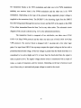
3.2.2 The Hardware Configuration of the 68HC12
68HC12 is available in 80 pin Quad flat pack (QFP) and 112 pin TQFP. In this
project of designing Physical Layer for the OBD II scan tool 80 pin QFP 68HC12B32 has
been used. Although 68HC12 can be used in several modes like EVB mode, JUMP-EE
mode, POD mode, and Back Ground Debug mode. Here in this project the EVB single
chip mode has been selected.
30
32-KBYTE FLASH EEPROM
'FP
VOL
V
V
SSA
DDA
Vsa*
1-KBYTE R A M
76S-BVTE EEPROM
ANO
AN1
AN2
ANO
AN4
AMS
AN8
AN7
ATD
CONVERTER
C P U 12
PERIOOICINTERRUP*
WKGU
SlNGLE WIRE
BACKGROUND
D E B U G MODULE
COf'WAICHDOG
r
CI DCK MONH'OR
RRFAK P O I N T S
IJJ
i'L:3
I STAR. - A f t h "
LITE
INTEGRATIOM
-IPfcO.MDDA
MODULE
IP>~L1 .' V»ODB
{LIM I
TJT3F
cc
<=ME5
SC
RxO
TxD
/O
)."0
SPI
t
nnmnmnn
MULTIPLEXED AODRESS/DAT A BUS
DDRA
DDRB
PORTA
PORT B
PWM
/O
u m m tttttttt
f-.. <j2l U l 3 " C i CM r-
WIDF
PAJS
a
« a«s «z i x i x i s s s
ESEceceixSliaE
££££281x2
0 0 0 0 0 0 0 0
§3522922
ct Q a a a a a c
MSCAN12
to
o
o
H-
CE
O
a.
PSC
PS I
PS2
PS3
PS4
PS5
PS6
PS?
P**~
pa,
p»2
PWO
PW1
PW2
PW3
a.
cc
o
o
l.-O
cc
P^'3
2
psi,
TsCAN
PuCAN
RxCAN
re AN;?
99233229
/O
2! '2 ^ ~ £ « a.
t—i
»— — »—»—
I— I— »— »— •— •— 1— »—
^ s / j * .-sj ^
(£j ^
<• % % s s s s s
(£$ £ $
«—»
O
0.0.0.0-13.0.0.0.
u> •* « o. •*- o
,f>
o
SDl-WISO
SDQ.WOSI
tttttttt
PTO
PT1
PT2
PT3
PT4
PTO
PTC
PT7
>OC1
T I M E R A M D ^ „ , »DC3
PULSE
® ; 7 K3C<1
ACCUMULATOR
IOCS
IDC6
I— 3».A|
PXTAl
XTAl
HLStt
PED
•et
PADO
PAD1
PADS
PAD3
PAD*
PADS
PADS
PAD7
WO
i.'O
i.'O
I.'O
^—* o
cc
8
PCANM
rijAN-i
IX.'. A N 6
l>CAN6
V— V- V— t— S— >— >— »—
< «C << *C < «C < ••*.
CD CD CD CD C2 CD *—• CD
NARROW BUS
Fig 3.3 Block diagram of MC68HC12BC32
As can been seen from the block diagram above the 68HC12 is comprised of eight
ports. They are A, B, DLC, E, AD, P, S, and T. Ports A and B have eight pins and
function as an address and data input output port in expanded modes. These ports can be
read or written at anytime. Data to be sent or received are written onto their respective
31
ports at registers $0000 and $0001. The direction of the data transfer depends on the data
direction register of the Ports at $0002 and $0003. In this project, Port A has been used to
transmit and or receive control signals to or from the Scan Tool internal bus. Port E pins
operate differently from ports A and B pins. Port E pins are used for bus control signals
and interrupt service requests signals. When a pin is not used in these specific functions,
it can be used as general purpose I/O. However, two pins PE[1:0] can be only used for
input, and the states of these pins can be read from data register even when they are used
for signal interrupts. BDLC pins can be configured as general-purpose I/O port DLC.
When BDLC functions are not enabled, the port has seven general-purpose I/O pins,
PDLC [6:0]. The BDLC function, enabled with the BDLCEN bit, takes precedence over
other port functions.
Port AD is used as Input to the analog digital subsystem and general purpose I/O.
When the analog digital functions are not enabled, the port has eight general purpose
input pins. Port P pins are shared by the four-pulse width modulation channel outputs.
When the pulse width functions are not in use, the port P eight pins can be used as
general-purpose I/O pins.
Port S is the 8-bit interface to the standard serial interface consisting of the serial
communications interface (SCI) and the SPI (Serial Peripheral Interface) subsystems.
When not in use with standard interface these pins can be used for general purpose I/O.
Port T provides eight general-purpose I/O pins when not enabled for Input capture or
Output compare in the timer and pulse accumulator subsystem. In this project, the
communication between the PC and the 68HC12 is done through the RS232 serial port.
32
The 68HC12 micro-controllers timer block has been used extensively used in this
thesis and detailed explanation is given in section 3.6. Besides this 68HC12 has a 32kbyte
Flash EEPROM block, a RAM block of Ik byte, an EEPROM block of 768 bytes, an SPI
and an SCI blocks for external communication, a PWM block, an interrupt handler block,
an oscillator block for clock signal generation, and most importantly the M68HC12 CPU.
3.2.3. Firmware
It is quite understandable that firmware is the main intelligence of the
microprocessor embedded system. It needs to be efficient, compact, and modularized. In
designing the physical layer of OBD II Scan Tool, the selected system supports were the
8 MHz clock, 1 kbyte ROM, and 768 bytes of EEPROM.
Firmware features include full support for either dumb terminal or host-computer
terminal interface, file transfer capability form a host computer to a RAM or EEPROM
allowing off board code generation, and ability to program EEPROM on either the host
EVB or a compatible target system. It also includes the D-bug 12 monitor/debugger
program resident in on-chip Flash EEPROM and single line assembler and disassembler.
3.3 Standard 68HC12 Timer Module
In this thesis the timer module of the CPU has been extensively used. The
detection programs detect the various occurrences of the frames as per the timing
constraints defined in SAE J1850 for the different protocols. This has been achieved
using the timer module of the CPU 12. The detail explanation of the timer module, the
control registers, counters are discussed in this section.
33
The standard timer module consists of a 16-bit software-programmable counter
driven by a prescaler. The timer can be used for many purposes, including waveform
measurements, while simultaneously generating an output waveform. It also can be used
to generate PWM signals without CPU intervention.
The purpose of the timer module is to allow for time critical operations to be
handled by the hardware, instead of trying to accomplish everything in software. For
example, generating waveforms or measuring waveforms is fairly straightforward using
the timer module. The standard timer module also has eight complete 16-bit input
capture/output compare channels, and one 16-bit a pulse accumulator. Each of these
features will be explained in more depth in brief later.
The Standard Timer Modules functions mostly involved doing things based on the
current value of the programmable timer. For example, when an 'output compare' occurs,
the hardware will automatically change the state of an output pin. Output compare means
that the current value of the timer matches a trigger value set by the software.
For another example, when an 'input capture' occurs, the current value of the timer
is stored in a special register. The input capture triggers when the state of one of the input
pins changes in a specified way. This allows us to capture the exact time of some external
event.
3.3.1 The Big Picture
The Timer block diagram from the MC68HC12B32 Technical Summary [6]
document (MC68HC12B4TS/D, chapter 12 Figure 18) is shown in Figure 3.6.
34
It shows the major components of the Standard Timer Module. Actually, it is
supposed to represent the functions relating to each pin. A complete diagram would
consist of 8 pins, and can be referred from the Figure 3.4.
zv
Fig. 3.4 Standard Timer block diagram
As can be seen in the diagram, there are lots of inter-related parts to the Timer
Module. Many of the parts are dual purpose depending on the mode the pin is operating
35
in (Input Capture or Output Compare). The important feature of this diagram is to show
how each pin has a relationship to the counter, TCNT.
3.3.2 The Timer System Control Registers
Before anything happens in the Standard Timer Module, the software on the CPU
must enable the timer system using the appropriate registers. The Timer System Control
Register (TSCR) is the key register to deal with. This register, located at register offset
$0086, controls the basic behavior of the entire timer module, such as whether, it is
running or not (Fig. 3.5).
RESET:
Bit 7
TEN
6
TSWAI
0
0
5
4
TSCBK TFFCA
0
0
3
0
2
0
1
0
0
0
0
0
0
0
Fig. 3.5 Timer System Control Register
This is a 8-bit register as shown in the diagram and can be read or written
anytime. It controls how the timer system operates in various modes such as Background
Debug Mode, WAIT state, and also how the timer flags are cleared. The Timer Enable
(TEN bit 7) bit of the register enables or disables the timer depending on its state. By
default it is in '0' state reducing the power consumption and disables the timer including
the counter. A T (bit 7) allows the timer to function normally.
3.4.3 The Timer Counter register
At the heart of the module is the Timer Count Register (TCNT). The TCNT
register is a 16-bit counter that is attached to the Module clock (MCLK), which is derived
36
from the CPU clock. Located at register offset $0084-$0085, this 16-bit counter is
initialized to zero. Once it starts counting (by setting Timer Enable in the TSCR), it
increments by 1 for each tick of the timer sections clock. There is a pre-scalar register
that allows you to change the relationship between MCLK and the TCNT register. The
TCNT 16-bit register is shown in Figure 3.6.
Reset:
Bit 15
14
13
12
11
10
9
8
Bit 7
6
5
4
3
2
1
0
0
0
0
0
0
0
0
0
Fig. 3.6 Timer counter register
TCNT is a free running counter, and will keep right on incrementing regardless of
the software state of the CPU. The next clock after TCNT reaches $FFFF will wrap it
over to $0000. The only states that stop the clock are the Wait and Background Debug
Mode. The affects of both are controllable in the TSCR.
The pre-scalar is a useful tool. The pre-scalar allows control of the amount of time
it takes for a single increment of the clock. By default, the prescalar is set to 1 on reset,
which means the TCNT register is incrementing at the MCLK speed. Normally, MCLK =
Crystal Frequency / 2 : MCLK on a 16-MHz crystal is 8mhz. (It is possible to change the
speed of MCLK by working with the CLKCTL register.) Using the PR0-PR2 bits of the
TMSK2 register, you can divide MCLK by up to 32. Table 3.2 shows the period of a
'tick' for an 8mhz MCLK. The TCNT duration shows the amount of time it takes for
TCNT to overflow (i.e., count from $0000 to $FFFF + 1).
37
Table 3.2. Prescalar value selection table
PR2
PR1
PRO
Pre-scale
Factor
0
0
0
1
0
0
0
0
1
1
1
0
1
2
4
8
1
1
0
0
0
1
16
32
1
1
0
1
1
1
Reser
ved
Reser
ved
(ns = nano-second, us = micro-second, ms = millisecond)
The newly selected pre-scalar factor will not take effect until the synchronized edge
where all prescaler counter stages equal zero.
3.3.4 The Timer Control Registers
The Timer Control registers are located from address offset $0088 -$008B. The
TCTL1 and TCTL2 are 8-bit registers that specify the output action to be taken as a result
of successful output compare. When either the output mode or the output level bit is one,
the pin associated with output compare becomes an output tied to OCn regardless of the
state of the associated data direction register.
The TCTL3 and TCTL4 control registers configure the input capture edge
detector circuits. Figures 3.7 and 3.8 show these 8-bit registers. The address offsets of
these registers are $008A (TCTL3) and $008B (TCTL4).
38
RESET:
Bit 7
EDG7B
6
EDG7A
5
EDG6B
4
EDG6A
0
0
0
0
3
2
EDG5B EDG5A
0
0
1
EDG4B
0
EDG4A
0
0
1
EDGOB
0
EDGOA
0
0
Fig. 3.7 Timer control register 3
RESET:
Bit 7
EDG3B
6
EDG3A
5
EDG2B
4
EDG2A
0
0
0
0
3
2
EDG1B EDG1A
0
0
Fig. 3.8 Timer control register 4
The default values of all the bits are reset to '0' disabling the capture. The table below
describes the various possible captures of the input signal (Table 3.3).
Table 3.3. Edge detector circuit configuration
EDGnB
EDGnA
Configuration
0
0
Capture disabled
0
1
1
0
On rising edge only
On falling edge only
1
1
Rising or falling edge
By default, the Timer Input Capture/Out Compare select register is configured to
input capture. Depending on the TIOS bit for the corresponding channel, the Timer Input
Capture registers are used to latch the value of the free running counter when a defined
transition is sensed by the corresponding input capture edge detector.
39
CHAPTER 4
DESIGN SOLUTION
4.1 Approach and Implementation
The new M68HC12 chip is a great step in a great direction. The 68HC12 has
more functionality, is directly applicable to real time applications, and packed into a
single chip design. This can be easily hooked onto a PC using the RS232 port and are
now widely available. All of this makes the M68HC12 an ideal candidate for this
research.
A microprocessor-based system was chosen to implement the 'Physical Layer' of
Universal OBD II Scan Tool. The hardware is an embedded micro-controller system
using Motorola's micro-controller, the 68HC12. The Physical Layer functionality is
achieved by assembly code written for M68HC12. The reason behind choosing the
M68HC12 is its architectural simplicity, low cost and wide availability.
A top-down approach was used to assure modularity of the system. The overall
functionality of the physical layer is to receive and transmit frames of data between the
OBD II system on the vehicle and the Data Link Layer residing on a PC. The frame
coming from the Data Link Layer is sent to the 68HC12 micro-controller, where based on
the type of protocol, it is encoded following the timing constraints. The micro-controller
system then transmits the frame to the OBD II system. While receiving a frame from the
OBD II system, the frame is decoded to an intermediate state using a hardware decoder
and is temporarily stored on the CPU 12. The frame is decoded further using a receiver
module to restore the original frame and this frame is then sent to Data Link Layer
residing on the PC.
40
In performing the operations, the different modular functionality that needs to be
supported are: Detection of the type of Protocol supported and a module to detect Start of
Frame, End of Data, Inter Frame Separation, End of Frame, Break, and Bit demodulation.
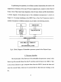
A Block diagram of the physical layer of the embedded microprocessor is shown in
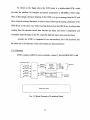
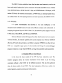
Figure 4.1. For proper interfacing to the OBD II bus, a Scan Tool Transceiver circuit is
needed. Descriptions of different modules are provided in the following sections.
PC
OBD II BUS
n
^
ii
68HC12
BASED
EVBU
—^"-ep—
^
"^
TRANSCEIVER
^r ^
^
<- ->
OBD II SCAN TOOL
- ^ ^
*<**>*
SOF, BRK, IFS, TIMEOUT
&
BIT-DEMODULATOR
Fig.4.1 Block Diagram of Embedded u-processor system for the Physical Layer;
4.2 Firmware Algorithm
The functionality of the firmware of the embedded microprocessor system in this
thesis to get the encoded frame from the PC and then send the frame to the OBD II. Then
in the reverse direction to get in response frame from the OBD II, decode the frame and
store the received frame, which can be accessed later by Data link layer residing on the
PC.
41
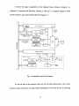
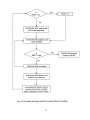
The main modules of the firmware are the MAIN Module, PROTOCOL_FIND
Module, and the Transmission module. The task of the MAIN module is to monitor and
perform the whole operation. It declares variables, initializes them, sets the baud rate,
initializes different flags, port directions, and the stack. It calls a particular module to
take over control depending on the user input. It also does a protocol finding operation
the first time communication established by activating the PROTOCOLFIND module.
Once the communication is established, it is left for the user to determine whether to send
a request message and to receive freeze data from the OBD II system on the vehicle, or to
analyze the proper functionality of the vehicle. The user can also send request signals to
the OBD II system and wait for an appropriate response for diagnosing a particular
module of the system. The control sequence of the module is shown in Figure 4.2.
The task of the PROTOCOLFIND is to establish communication or interface
with the OBD II device and then try to find out the protocol that is being supported by the
system. This is achieved by sending a request message in the diagnostic format specified
in SAE J1850 and wait for the appropriate response. Different interrupt conditions, like
TIME OUT, are kept on watch while finding the protocol and also while waiting for a
response from the OBD II system. When these situations take place, normal operation
terminates and the system indicates that a particular interrupt has occurred.
Once the valid protocol is detected the control is transferred to the Transmission
module. Depending on the user's request, this module will send a request or receive a
message from the OBD II system. In doing so, it will indicate various flag occurrences,
SOF, EOF, EOD, IFS and watch for the break flag. Once it decodes a frame it stores the
42
frame to be accessed by the data link layer, residing on the PC. The control flow for the
Transmission module is shown in Figure 4.4.
Variable Initialization
I
Baud rate setting, stack
initialization, Enable Timer
NO
i
I
Run Protocol find Module
1
Transmit module for finding
protocol on the OBD II bus
and at the same time watch for
interrupts
Transmission Mode Module
I
Receive frame from OBD II
bus and at the same time watch
for interrupts.
I
Module to transmit frame to
the OBD II bus and at the same
time watch for interrupts
Analyze the Frame for
Protocol validity
YES
Module to receive frame from
the OBD II bus and at the same
time watch for interrupts
I
Check for Next Protocol
Provide the frame for PC
i
END
Fig. 4.2 Flowchart of Main Module, for M68HC12 micro-controller;
The assembly language codes for the firmware have been included in Appendix.
43
4.3. Software
The purpose of the Universal OBD II Scan Tool's lower level software routines
for the Physical Layer on the PC side is to establish linkage between the Data Link Layer
and the external hardware of the Physical Layer. The first step to establish linkage is to
find the protocol. This is done by the PROTOCOL_FIND module. The detailed algorithm
for this module is shown in Figure 4.3.
A request message for the first protocol type is sent following the diagnostic
message format specified in SAE J1850. Details of the diagnostic message are discussed
in section 3.4. The bytes are sent serially via an I/O port. Depending on the timing
constraints of the protocol ' 1 ' and '0"s are sent. There are only two data bytes that are to
be sent while finding the protocol. Mode $01 byte and PID $00 byte, are sent. The
message length is determined by the mode. This enables the tool to check for proper
message length and to recognize the end of message without waiting for possible
additional data bytes. Once the total message has been sent, the tool waits for the
response message from the OBD II system.
For SAE J1850 network interfaces, the on board systems should respond to a
request within 100ms of a request or a previous response. With multiple responses
possible from a single request, this allows as much time as would be necessary for all
modules to access the data link and transmit their responses. If there is no response within
this period, the tool can either assume no response will be received or if a response has
already been received, that no more responses will be received.
44
Variable Initialization
I
Send a request message
ModeSOl andPIDSOOfor
I
Module to receive response
data from the OBD II svstem
Yes
Decode and store the
resoonse data
I
Analyze the data for PWM
Send a request message
ModeSOl andPIDSOOfor
No
L
Module to receive response
data from the OBD II svstem
Yes
Decode and store the
resoonse data
I
Analyze the data for VPWM
Set T_Out Flag
Fig. 4.3 Flowchart of PROTOCOLFIND module for 68MHC12 microcontroller.
45
The response message is received serially through the I/O port, this message is
decoded and is temporarily stored. This message is analyzed to recognize the protocol
supported. If a Mode $01 and PID $00 is received, the protocol interface that is supported
can be determined. If this is not the case, control is returned to the request-send module
where it checks whether all protocols have been tried or not. If not it will send a request
diagnostic message for the second type protocol. The transmission of a frame and the
wait for interrupts is similar. Once it receives a response message, it is decoded and
stored temporarily and then later analyzed to check for proper protocol.
The protocol find module sets or resets the protocol flag, indicating to the main
module whether it is successful or not in finding the protocol supported by the system.
The Main module then takes appropriate action, by indicating to the user whether the
operation was successful or not.
Once the type of protocol has been detected, the main module transmits the
control to the transmission module. The user can then either send a request or receive a
response from the OBD II system.
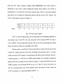
Depending on the user's choice the respective modules for transmitting or
receiving are called by the transmission module. The microprocessor is now ready to
send or receive messages from the OBD II system. These modules activate the various
detection programs, which set or reset the different flags for start of frame, end of data,
inter frame separation, end of data, and break flags. The bit modulation detector detects
the bits and stores the value temporarily. These are formed into a frame and can be
accessed by the data link layer residing on the PC later. The Control flow for various
detector modules is shown in Figure 4.4.
46
No
Mode = Tx
Activate the 'SOF' module and
wait for the occurrence.
Activate the Bit modulator, and
watch for BRK.
Yes
Transfer the program
control to MAIN
Watch for EOD occurrence
Activate the EOF detector, and
watch for its occurrence.
Activate the IFS detector, and on
occurrence the system would be
readv to transmit or receive frame.
Fig. 4.4 Flowchart showing control flow among Detector modules.
47
4.4. Diagnostic Message Format
This message format is used to detect the type of protocol that is being supported
by the vehicle. To confirm to the SAE J1850 limitation on the message length, diagnostic
messages are limited to a three-byte header, and have a maximum of 7 data bytes, as
shown in Table 4.1.
Table 4.1. Diagnostic message format
Header Bytes (Hex)
Priority Target
Source
/type
Address address
Data Bytes
#i
#2
#3
#4
#5
#6
#7
ERR
RSP
Diagnostic Request at 10.4kbps (J1850 and ISO 914]1-2)
68
6A
Fx
Maximum 7 data bytes
Yes
No
Diagnostic Response at 10.4kbps (J1850 and ISO 9141-2)
Yes
48
6B
Addr
Maximum 7 data bytes
No
61
Diagnostic Rec [uest at 41.6kbps (J1850)
6A
Fx
Maximum 7 data bytes
Yes
No
41
Diagnostic Response at 41.6kbps (J 1850)
6B
Addr
Maximum 7 data bytes
Yes
No
The first three bytes of all diagnostic messages are the header bytes. The value of
the first header byte is dependent on the bit rate of the data link and the type of message.
The second header byte has a value that depends on the type of message, either request or
a response. The third header byte is the physical address of the device sending the
message and is generally $F1 for an OBD II scan tool.
The maximum number of data bytes available to be specified by SAE J1850 is 7.
The first data byte following the header is the test mode, and the remaining 6 bytes vary
depending on the specific test mode. For modes $01 and $02, the PID determines
48
message length. This enables the tools to check for proper message length, and to
recognize the end of the message without waiting for possible additional data bytes.
All the diagnostic messages use cyclic redundancy check (CRC), as defined in
SAE J1850, as an error detection (ERR) byte. The In-frame response (RSP) byte is
required in all request and response messages at 41.6kbps, and is not allowed for
messages at 10.4kbps. The purpose of Mode$01 is to allow access to current emission
related data values. The request for information includes a Parameter Identification (PID)
value that indicates to the on-board system the specific information requested.
The on-board module will respond to this message by transmitting the requested
data value last determined by the system. PID $00 is a bit encoded PID that indicates, for
each module, which PID's that module supports. PID $00 must be supported by all
systems which respond to Mode $01 request, because diagnostic tools that conform to
SAE J1978 use the presence of a response by the vehicle to this request to determine
which protocol is being supported for OBD II communications. As mentioned only when
a message is received with Mode$01 and PID $00, can the protocol be determined.
4.5. Transceiver Circuit
This circuit is more extensively described in the Master's thesis, "Design of
Universal Scan Tool" written by Sarwar Sohail [6]. Therefore for the convenience of the
reader, the transceiver circuit design has been dealt here in brief. The author recommends
the reader refer to the above-mentioned thesis for full details. Different types of protocols
supported by OBD II system have different voltage levels. Hence, to provide proper
interfacing of the scan tool with the OBD II bus, the transceiver has been designed. It
49
transforms TTL voltage levels of the internal scan tool bus to OBD II bus voltage levels
(depending on the type of protocol used) while transmitting the frame and does the
opposite function while receiving the frame from the OBD II bus.
The OBD II bus is a sort of OR bus. This means, if two or more nodes try to send
a message over the OBD II bus at the same time, then the bit with the longer active
voltage (high) level will arbitrate over the bit with shorter active voltage level or passive
(low) voltage level. Accordingly, the node supplying that bit will win the bus and other
nodes will yield. The transceiver circuit designed supports this performance.
VPW
PWM
VBAT
POWER SUPPLY
SWITCHING
REALY CIRCUIT
POWER SUPPLY " 0 TRANSMIT MODULE
VDD
OUT
OUTMODE
TRANSMIT
MODULE
FOR VPW
RECEPTION
MODULE
FOR VPW
ORED BUS
BUSRCV
BUS
OR BLOCK
OUT
OUTMODE
PWM
TRANSMIT
MODULE FOR
PWM
RECEPTION
MODULE FOR
PWM
Fig. 4.5 Block Diagram of Transceiver Circuit
Functionally, the Transmitter circuit, as shown in Fig. 4.5 is comprised of one
power supply selector block, two transmitter blocks, and two receiver blocks. One of the
50
two transmitter blocks is for VPW modulation and other one is for PWM modulation;
similarly one receiver block is for PWM modulation and the other one is for VPW
modulation. Depending on the type of the protocol being supported, proper voltage is
supplied to the transmitter block. The BUSRCV is the incoming signal from the OBD II
bus after being passed through the receiver circuit; and the BUS is the signal on the OBD
II bus either transmitted from the Scan Tool or any other nodes. The schematic circuit
diagram of the circuit is shown in Fig. 3.19, in the aforementioned thesis.
The transmitter block is composed of two sub-blocks, one takes care of SAE
J1850 41.6 Kbps PWM protocol and the other one takes care of SAE J1850 10.4 Kbps
VPW protocol. The receiver block is designed with 3 op-amps and a few other logic
gates. For input from OBD II bus op-amps compare the signal voltage on the bus with a
predefined thresh hold voltage. If the bus voltage is greater than the thresh hold then it is
considered to be active (high) and if it is lower than the thresh-hold then the signal is
taken as passive (low). The supply voltage selector circuit is constructed with a couple of
relays, a couple of transistors, and few resistors. Depending on the type of protocol used
one of these relays is activated and proper voltage is routed to the circuit.
51
CHAPTER 5
RESULTS
This chapter summarizes the results, with sample data, which indicate the proper
functionality of the different modules. Due to memory constraints on the chip,
verification of the detector codes was done at the modular level. The success of each
individual detector program fulfils the objective of this thesis. Integration of all modules
is yet to be done and once integrated the assembly code can be tested and verified on a
vehicle.
5.1 Bit Modulator and PRT FIND Module Verification
The main function of the Physical layer is the establishment of an interface
between the OBD II system and the application layer. In performing this task, the system
has to determine the protocol supported and allow the user to transmit or receive data
from the OBD II system.
An assembly language program was written to test the type of protocol supported.
Accordingly, the PROTOCOLFIND module consists of a transmitting module and a
receiving module. These modules were tested using sample data for both types of
protocols. While transmitting, the data was observed on a Fluke oscilloscope and the
screen capture was done by Fluke combi-scope software, which gives the data waveform
in bit map files. Figure 5.1 shows the output of the Transmit module for 5 bytes of
sample data for the PWM protocol. Figures 5.2-5.6 show each byte of the output
52
waveform, which follow the timing requirements of the protocol indicating the proper
functionality of the generated signal.
As shown in Figure 5.1, for the PWM protocol, a " 1 " bit is characterized by a
rising edge that follows the previous rising edge by at least Tp3 (> 23 JLI sec). Two rising
edges are never closer than Tp3 and the falling edge occurs Tpl (8 ja sec normally) after
the rising edge. Similarly, a "0" bit is characterized by a rising edge that follows the
previous rising edge by at least Tp3 ( 23 (j, sec). Two rising edges are never closer than
Tp3 and the falling edge occurs Tp2 (> 15 JJ, sec) after the rising edge.
-10.0000
•15.0000
.
-20.0000
0.00 ms
1 ms/Div
Fig. 5.1 5 byte sample data transmitted by PWM transmit protocol.
53
Channel 1
10.0000
i—i—
8.7671
7.5342
6.3014
5.0685 V
rwn/N.,
rvy
"y
.
"MVVy
AJ\>^<
'i~\
V^WM
f^-^wvy
N
3.8356
2.6027
1.3699
tu—!
0.1370
88 ns
^Artne-1
rA/Wi n
W.\.
•-VA/NrV
I—W
\I\U\I—\
25 iJis/Div
Fig. 5.2. First byte ($68) of the PWM sample data.
In Figure 5.2 after the first rising edge, the falling edge occurs after 16 u sec
followed by a rising edge occurring after 8 u sec of the previous rising edge (passive
pulse of 8 u sec) indicating a '0' bit. The second rising edge follows the first after 24 u
sec, and the falling edge occurs after 8 u sec (active pulse length) depicts a ' 1' bit. The
T and '0' bit pattern in Figure 5.2 is '0' ' 1 ' ' 1 ' '0' ' 1 ' '0' '0' '0' which is 68 in
hexadecimal. With similar bit definitions the pattern followed in Figures 5.3-5.6 indicate
a 6A, FI, 01, 00 in hexadecimal for PWM protocol.
54
Fig. 5.3. Second byte ($6A) of the PWM sample data.
Channel 1
10.0685
8.8185
7.5685
6.3185
5.0685 V
om/Yi
V»>1
P-^VV\
fWTA
^ !
3.8185
2.5685
1.3185
0.0685
K
30 ns
\rvw—V
r^KTU
•—VY^
v—WVN
v-^r
\
AC
24 ns/Div
Fig. 5.4. Third byte ($F1) of the PWM sample data.
55
VWVl
VAA/VJ
Channel 1
10.2740
f
r
r
•
•
•
•
8.9726
7.6712
6.3699
5.0685 V
rv
1A//"~"V\
lA/V^TM
KU
!v
IA/VTI
r
Via
1
tAyVW
!
3.7671
AA
2.4658
1.1644
JVJ
-0.1370
*—^
WV
-
KV\/\J
268 ns
LAAH
U**/>l
Lyv\m
ivwvJ
'v
r-^j-
24 ns/Div
Fig. 5.5. Mode byte ($01) of the PWM sample data.
Channel 1
10.0685
8.8185
7.5685
6.3185
5.0685 V
V\AJ'
^rvvu
l I
^vvu
Jv'vu
^JVVU
/Ul
^JVVO
HUL,
3.8185
2.5685
1.3185
0.0685
v
31 ns
I^JTV
'VW
KST-NT
'-/\
k//W
V\j"J
24 ns/Div
Fig. 5.6. PID byte ($00) of the PWM sample data.
56
>JWJ
r\AA"
The generated data is given as an input to the receiver code of the PRTFIND
module, and the results obtained match the actual transmitted data indicating the proper
working of the code in detecting the data transmitted.
Input data: $68 $6A $F1 $01 $00.
Output data: $68 $6A $F1 $01 $00.
Figure 5.7 shows the output of the Transmit module for 5 bytes of sample data for
the VPWM protocol. Figures 5.8-5.12 show each byte of the output waveform.
Channel 1
10.5250
5.5250
0.5250
-4.4750
-i
-9.4750V
-14.4750
460 ns/Div
Fig. 5.7. 5 byte sample data transmitted by VPWM transmit protocol.
The results follow the timing of the protocol indicating the proper functionality of
the transmitter code. As shown, a " 1 " bit is either a Tv2 (128|j, sec) passive pulse or a
Tvl (64 JLA sec) active pulse. Conversely, a "0" bit is either a Tvl (64 |i sec) passive pulse
or a Tv2 (128 (a sec) active pulse. The end of the previous symbol starts the current
symbol in this protocol. In this generated signal, the active pulse lengths are used to
define the bits for VPWM protocol.
57
Channel 1
U
U
89 ns/Div
Fig. 5.8. First byte ($61) of the VPWM sample data.
In Figure 5.8, the first active pulse is of length 128 u sec which indicates a '0' bit.
The next active pulse of length of 64 u sec is indicating a bit ' 1 ' . As shown, the pattern
followed in Figure 5.8 is '0','1', ' 1 ' , '0', '0', '0', '0', ' 1 ' , which is w61' in hexadecimal.
Unlike PWM, in VPWM the end of the previous symbol starts the current symbol. In this
case, since the passive pulse is much less than the minimum length (64 u sec) required to
identify it as a bit, the bit detector ignores it and waits for next rising edge.
Similar bit patterns of l's and 0's in Figures 5.9-5.12 indicate a
'FI ','01 ','00' in hexadecimal for VPWM protocol.
58
W
6A',
Channel 1
7.9653
tMWAfiMMWWf
5.5026
r
w-vwwv^^-w^
^ T ^ A \
k J * W A W J \ J J j
3.0399
0.5772
V"*
^J^/J
-
-1.8854 V
-4.3481
81 ns/Div
Fig. 5.9. Second byte ($6A) of the VPWM sample data.
Channel 1
6.3213
i
„..,....
1
•
'S
4.3624
2.4034
0.4444
v V
r
i
1"
:
J
J
J
IJ
J
N
!
-1.5145 V
1
I
•
„
-3.4735
75 ns/Div
Fig. 5.10. Third byte ($F1) of the sample data.
59
:
IJ
fl
•
7.3862
5
•'•
0167
J
i
j — * ~ 1
2.6473
u
0.2779
-2.0915 V
u
>
u
": \
-4.4609
102ns/Div
Fig. 5.11. Mode byte ($01) of the VPWM sample data.
109ns/Div
Fig. 5.12. PID byte ($00) of the VPWM sample data.
The output signals from frame originators are fed as input to the receiving module
and the output of the receiver module are stored temporarily at memory location RSDAT,
which is then verified.
Input data: $61, $68, $F1, $01, $00.
Output data: $61, $68, $F1, $01, $00.
60
The results obtained match the input indicating proper functioning of the Bit
demodulators of both types of protocol and thereby the receiver module codes. The
Protocol Find module uses the transmitter module for transmitting a request message and
waits for a response message. The receiver module receives this message and analyzes it
to find the protocol supported.
5.2. SOF. EOD. EOF Detectors Verification
The Start of frame, End of Data, and End of Frame, signals were been generated
for VPWM protocol and the outputs are shown in Figures 5.13 and 5.14.
Channel 1
10.5000
~i—i—i—',—;—r~~r~
Dnnnnj
5.5000
0.5000
-4.5000
-9.5000V
498 ns/Div
Fig 5.13 The SOF and EOD marks for VPWM.
The Start of Frame (>180 us active) mark has the distinct purpose of uniquely
determining the start of a frame and the End of Data (>180us Passive) is used to signal
the end of transmission by the originator of a frame.
The generated signal is a sample with SOF mark (first active pulse), a frame of
5bytes (active pulses of different lengths as described in previous section) and the EOD
frame is seen as the last passive pulse of 180 u sec in length. The sample data follows the
timing constraints of VPWM protocol.
61
The SOF detector is activated which detects the SOF frame, after which the Bit
detector takes over to decode the bits in the frame until an EOD is encountered. Once the
EOD is detected the Bit detector terminates its normal operation until the SOF detector
again detects a SOF mark. The input and output data of the receiver module are shown in
Figure 5.14. As can be seen, the Bit modulator detects the signal only after a SOF is
detected, and once it detects a EOD frame it waits for another SOF before detecting the
bits again.
Input: SOF, $61,$6A,$F1,$01,$00, EOD.
Output frame: $61,$6A,$F1,$01,$00.
The output of the frame originator is fed as an input to the SOF, EOD and Bit
Detectors. The outputs of the receiver module match input frame indicating the proper
functionality of the codes of SOF and EOD detectors.
Channel 1
10.3116
5.3302
0.3489
u
\
-4.6325
~
u
-9.6138 V
' • • • •
:••
590ns/Div
Fig. 5.14 EOF after 2 sample frames for VPWM.
Figure 5.14 shows an EOF mark (> 261 us) in addition to SOF and EOD marks.
The completion of the EOF defines the end of a frame (by definition, an EOD forms the
first part of the EOF, as shown in Figure 2.3. After the last transmission byte (including
62
in-frame response byte where applicable), the bus will be left in a passive state. When
EOF occurs, all receivers will consider the transmission compete. The input and output
data of the receiver module are shown below. As can be seen, the Bit modulator detects
the signal only after a SOF is detected, and once it detects a EOD frame it waits for
another SOF before detecting the bits again.
Input: SOF, $61,$6A,$F1 EOD $61,$6A,$F1 EOF.
Output frame: $61,$6A,$F1, $61,$6A,$F1.
Once the EOF is detected, the bit detector terminates its normal operation. It
activates again only after the Transmission module indicates to the receiver to receive a
frame, and the SOF flag is set by the SOF detector.
The output of the frame originator is fed as input to the SOF, EOD and EOF
detectors. The output of the receiver module matched the input frames indicating the
proper functionality of the codes of SOF, EOD and EOF detectors.
The Start of frame, End of Data, and End of Frame, was generated for the PWM
protocol as well and the generated signal is shown in Figure 5.15.
63
10.3116
5.3302
0.3489
Channel 1
'"
i
t
"t
r
r"
J
"
i" "
i.
<-
•
mmmmmmuMWwmu
-4.6325
-9.6138 V
J
i
i
i...
115ns/Div
Fig. 5.15 EOF after 2 sample frames for PWM
The generated signal is a sample with a SOF mark, a first frame of 2bytes, a EOD
frame, followed by a SOF mark, a second frame of 2 bytes and an EOF mark. The sample
data follows the timing constraints of VPWM protocol. The Start of Frame is the first
active pulse of 32 u sec followed by, at least a 16 ^i sec passive pulse. The SOF mark has
the distinct purpose of uniquely determining the start of a frame. The pulses following the
SOF mark form bits of the frame as described in the previous section. The End of Data
follows the last bit and is 48us passive, normally with reference to the last rising edge.
This is used to signal the end of frame. Similarly the second SOF mark is an active pulse
of 32 u sec and a passive pulse of 16u sec following the EOD mark. The EOF mark is
recognized by the last passive pulse of at least 70us after the last rising edge. After the
last transmission byte, the bus will be left in a passive state. When EOF has expired (Tp5
after the rising edge of the last bit), all receivers will consider the transmission compete.
The input and output data of the receiver module is shown below, as can be seen
the Bit modulator detects the signal only after a SOF is detected, and once it detects a
EOD frame it waits for another SOF before detecting the bits again.
Input: SOF, $61, $75, EOD $61, $75 EOF.
64
Output frame: $61, $75, $61, $75.
Once the EOF is detected, the bit detector terminates its normal operation. It
activates again only after the Transmission module indicates the receiver for a frame, and
after the SOF detector sets the SOF flag. The output of the receiver module indicates the
proper functioning of the SOF, EOD, EOF and Bit detector modules for PWM protocol.
The Time Out detector module verification has not been discussed since this
comes into play only while communicating with the vehicle, which has not yet been
attempted. Once the integration of the modules is done, verification of the Time out
assembly code can be easily achieved.
The timing requirements are fulfilled as shown by tests of all the modules,
indicating success at the modular level. Once a frame has been received from the PC by
the main module it is sent to the Transmission module where it is transmitted with all the
required frames. The receiver module then receives the response message from the OBD
II system where all the detection modules come into play. After the detection of the frame
it is sent to the main module to be transmitted to the PC. Proper functioning of the
modules indicates that the code can receive and transmit data to and from the OBD II
system.
5.3 BRK Detector Verification
The Break signal was generated for VPWM protocol and the output is shown in
Figure 5.16. The VPW Break symbol will be detected as an "Invalid" symbol, which will
then ignore the current frame, if any. The VPW Break symbol is a long active period (>
280 JJ. sec), followed by a IFS symbol which is a long passive period (>280 \i sec).
65
The generated signal is a sample with SOF mark, a frame of 2bytes EOD mark
followed by another set of SOF, frame of 2bytes EOF mark, a SOF mark and finally a
BRK signal. The Break signal can be recognized in the figure as the last active pulse of
300 u sec followed by a passive period of 300 u sec.
Channel 1
10.1832
5.2205
-9.6675 V
502 ns/Div
Fig. 5.16 SOF, EOD, EOF and BRK marks for VPWM.
BRK is allowed to accommodate those situations in which bus communication is
to be terminated and all nodes reset
The output of the frame originator is fed as input to the receiver module, which on
detection of Break symbol terminates the operation ignoring the last frame before break
signal.
Input: SOF, $61, $6A, EOD, SOF, $61, $6A, EOD, $..., BRK.
Output frame: $61, $6A, $61 $6A.
The output of the receiver module indicates the proper functionality of the break
detector module for VPWM protocol.
Figure 5.17 shows the generated break signal for PWM protocol. The generated
sample data is a signal with SOF mark, a byte of data, EOD mark, followed by another
set of SOF mark, a byte of data, EOD mark and a BRK signal.
66
BRK in PWM is allowed to accommodate those situations in which bus
communication is to be terminated. The BRK symbol can be recognized as the last active
pulse of 40 u sec from the Figure 5.14.
10.1750
5.1750
0.1750
-4.8250
-9.8250 V
82 ns/Div
Fig. 5.17 Two frames and a Break signal for PWM
The PWM Break symbol (40 \i sec active) is an extended SOF symbol and will be
detected as an "individual" symbol to some devices, which will then ignore the current
frame, if any. Following the break symbol, an IFS symbol (120 LI sec) is needed to
synchronize the receivers.
The output of the frame originator is fed as input to the receiver module, which
on detection of Break symbol terminates the bus communication.
Input: SOF, $68, EOD, SOF, $68, EOD, BRK.
Output frame: $68, $68.
The output of the receiver module indicates the proper functionality of the break
detector module for PWM protocol. After detection of a break symbol, the control is
transferred to the main module.
67
CHAPTER 6
CONCLUSIONS
A microprocessor-based Physical layer for On Board Diagnostic II (OBD II) scan
tool has been designed in this project. An embedded microprocessor, Motorola's 68HC12
has been used to design the physical layer. This chapter also gives some direction for
future developments to make the system more efficient and concise.
Although OBD II supports three types of protocols, which are SAE J1850PWM at
41.6kbps, SAE J1850VPWM at 10.4kbps and ISO 9141-2, only two of these, the PWM
and VPWM are currently in use in the USA and are treated here. To make the code
simpler, for this thesis, the 68HC12 microcontroller has been used in the single chip
mode. The lack of memory on the development board used, required individual testing of
the modules to verify proper functionality. Debugging the code proved difficult because
the debug commands supported by the assembler terminate on encountering branch
statements, which are used in the code frequently.
The implementation and verification of the assembly code has been done at the
modular level using test signals and sample data. The test signals were generated to
simulate real-time operation. The signals generated by the transmitter module indicate the
functionality of the module and indicate that frames of data can be transmitted to the on
board system for both types of protocol supported. The output is used to verify the
receiver module. The timing of the waveforms have been verified using a Fluke
oscilloscope. The wave shapes monitored by the oscilloscope are found to be slightly
distorted but within the acceptable limits. The output of the receiver module matched the
68
input data indicating the proper functioning of the various detector modules used in the
module for detecting the transmitted frame.
Although the modules have been integrated into one huge assembly code, the
code could not be tested due to memory limitations. However, the modular level test
shows that the assembly code in the 68HC12 can replace the physical layer of the OBD II
scan tool. This design requires minimum hardware, is simple and cost effective. The
code can be upgraded for future developments in the field by adding a few modules and
changing a few lines of code.
The current development also shows the design of the physical layer of the OBD
II using a microprocessor is simpler, uses minimum hardware, and is more accurate at
measuring the different frames and bits. The physical layer can now be easily connected
to a PC eliminating connecting hardware and making it relatively easy for the data link
layer to store the retrieved data from the vehicle.
At this point, the author suggests that using the micro controller in expanded
memory rather than single chip mode would offer more memory, which may achieve an
efficient design at the expense of speed. The programmer issue, of using expanded
memory, has a draw back. To program the EEPROM or the FLASH, a programmer such
as BDM interface board is needed. This needs special hardware as well. Alternatively a
better microprocessor, like a 68333, can be used which is sure to reduce the code
considerably and can eliminate some of the memory problems. The use of a 68333 microcontroller is sure to enable the design of a highly efficient system, but it will make the
project considerably expensive. The efficiency might pay off this cost consideration.
69
In conclusion, it can be inferred that the significance of the design of Physical
Layer of OBD II Scan Tool, using a microprocessor is suggested, which will simplify and
increase the versatility of the system. Using a microprocessor-based system as the
physical layer indicates the feasibility of developing a PC-based universal scan tool in
future.
70
REFERENCES
[1] Society of Automotive Engineers, Inc., "OBD II scan tool-SAE J1978 JUN 94," SAE
On-Board Diagnostics for Light and Medium Vehicles Standards Manual,
Warrendale, PA, 1995, pp. 25-28.
[2] Society of Automotive Engineers, Inc., "E/E Diagnostic Test Modes-SAE J1979 JUN
94," SAE On-Board Diagnostics for Light and Medium Vehicles Standards Manual,
Warrendale, PA, 1995, pp. 29-32.
[3] Society of Automotive Engineers, Inc., "Class B data communications network
Interface SAE J1850 MAY94," SAE On-Board diagnostics for Light and Medium
Vehicles Standards Manual, Warrendale, PA, 1995, pp. 95-111.
[4] Godavarthy, Sunitha, "Design of Universal Scan Tool," Master's Thesis, Department
of Electrical Engineering, Texas Tech University, May 1998.
[5] Sarwar Sohail, "Design of Physical Layer for Universal Scan Tool," Master's Thesis,
Department of Electrical Engineering, Texas Tech University, May 1998.
[6] Motorola Inc., Technical Summary for MC68HC912BC32/16-Bit Microcontroller,
Motorola Literature Distribution, Denver, CO, 1997.
[7] Motorola Inc., 68HC12 Reference Manual, Rev 1, Motorola Literature Distribution,
Denver, CO, 1997.
[8] Greenfield, Joseph D, The 68HC11 Microcontroller, Saunders College publications,
Fort worth, TX, 1992.
[9] "Programming 68HC12", http://www.seattlerobotics.org/encoder/oct97/68hc 12.html,
Encoder, Newsletter of Seattle Robotics Society.
[10]"68HC12 Timer Module," http://www.seattlerobotics.org/encoder/nov97/68hc 12.html,
Encoder, Newsletter of Seattle Robotics Society.
[11]"68HC12 Resource homepage," http://redhat.eng.wayne.edu/, Wayne State University.
71
APPENDIX
FIRMWARE Codes:
**************************************************+**********+**********
Main Program for OBD II scan tool physical layer
Written for Motorola M68EVB912B32 Eval Board
Written for AS 12 Assembler by Shyam Kallepalli
CONSTANTS SETTING=
PORTA
PORTBEQU
DDRA EQU
DDRB EQU
TIOS EQU
TCNT EQU
TSCR EQU
TCTL4 EQU
TMSK1EQU
TMSK2EQU
TFLG1 EQU
TCO EQU
TC7 EQU
PORTTEQU
DDRT EQU
PORTSEQU
DDRS
SCOBDH
SCOBDL
SCOCR1
SCOCR2
SCOSR1
SCODRL
EQU
$0001
$0002
$0003
$0080
$0084
$0086
$008B
$008C
$008D
$008E
$0090
$009E
$00AE
$00AF
$00D6
EQU
EQU
EQU
EQU
EQU
EQU
EQU
$0000 ;Port A Register of HC12
;Port B Register of HC12
;Data Direction Register Port A
;Data Direction Register Port B
;Timer Input Capture, Output Compare Select
; 16 Bit Free Running Counter
;Timer System Control Register
;Timer Control Register 4
;Timer Mask 1
;Timer Mask 2
;Timer Interrupt Flag 1
;Timer Input Capture / Output Compare Register 0
;Timer Input Capture / Output Compare Register 7
;Port T Data Register
;Data Direction Register for Timer Port
;Port S Data Register
$00D7 Data Direction Register
$00C0 SCI baud rate control register
$00C1 SCI baud rate control register
$00C2 SCI control register 1
$00C3 SCI control register 2
$00C4 SCI status register 1
$00C7 ;SCI data register Low
VARIABLE DECLARATIONS^
PWM FDB
VPM FDB
PRTCL FDB
MODE FDB
ERROR FDB
72
End of VARIABLE DECLARATIONS:
*
Main Module
ORG $0800
LDAA #$00
STAA DDRB
*
; Start of the program
;Load '00' onto the data direction register
;of portB to make it as input port.
LDAA #$02
STAA DDRS
LDD
STD
#52
SCOBDH
; Equivalent 9600 baud rate
; sets the baud rate
LDAA #$C8
STAA SCOCR2
;Set the TE,RE and TIE
LDAB #$C0
STAB SCOSR1
;Set TDRE TC bits
=END OF INTIALIZATION=
MAIN JSR
BI
B9
B3
B2
PRT FIND
LDAA
CMPA
BNE
BRA
LDAA
CMPA
LBNE
LDAA
CMPA
BNE
LDAA
STAA
SWI
PRTCL
#$FF
BI
B9
PWM
#$FF
B2
VPM
#$FF
B3
ERROR
#$FF
JMP
JSR
LDAA
CMPA
LBNE
LDAA
CMPA
B6
M FIND
MODE
#$FF
B4
MODE
#$AA
Jump to subroutine PRT_FIND to find the
protocol supported by the OBDII system.
Load the PRTCL flag and
compare with 'FF' if high
branch to bl to find which protocol else
branch to B9 to indicate error and terminate.
Check whether it is PWM
compare PWM. If it is set
branch to B2 to find out the mode,else
check whether it is VPWM
Compare VPM. If it is set
Branch to B3 to find out the mode, else
Load 'Error' with *FF* indicating
Undefined protocol and terminate.
End of the program.
;Jump to B6 to find out the mode for VPWM
;Jump to subroutine Mfind to find out the mode
;Check whether the mode is transmitting by
;comparing with 'FF' if so
;branch to B4, else
;Check the Mode is receiving by comparing
;with'AA'ifso
73
BNE
LDAA
STAA
LBRA
B5
MODE
#$00
B2
;branch to B5, else
;Load mode with '00* indicating
;that the system is in FREEZE
;branch to B2 to find Mode.
JSR
PWM_TX
BRA
JSR
B2
PWM_RX
BRA
B2
;Jump to PWMTX to detect the different frame
;occurrences while transmitting.
;Branch to B2.
;Jump to PWMTX to detect the different frame
;occurrences while receiving.
;Branch to B2.
B6
JSR
LDAA
CMPA
BNE
LDAA
CMPA
BNE
LDAA
STAA
M FIND
MODE
#$FF
B7
MODE
#$AA
B8
MODE
#$00
;Jump to subroutine Mfind to find out the mode
;Check whether the mode is transmitting by
comparing with 'FF' if so
;branch to B7, else
;Check the Mode is receiving by comparing
;with'AA' if so
;branch to B8, else
;Load mode with '00' indicating
;that the system is in FREEZE
B7
JSR
VPM_TX
B8
BRA
JSR
B6
VPM_RX
BRA
B6
; Jump to VPMTX to detect the different frame
;occurrences while transmitting.
;Branch to B6.
;Jump to VPMRX to detect the different frame
;occurrences while receiving.
iBranch to B6.
B4
*
B5
*
*
PRT_FIND
CALL
RTS
PRTFIND
;Call the module to find PROTOCOL
;return to main
M_FIND
CALL TXMODE
RTS
;Call the module to find Transmission mode
;return to main
VPM_ TX
" CALL FROM PC
CALL TXVPWM
RTS
;Receive frame from PC
;Call the module to transmit VPWM frame
;return to main
VPM_ RX
" CALL RXVPWM
CALL TO_PC
RTS
Call the module to receive VPWM frame
transmit the Frame to PC
return to main
PWM TX
CALL FROM PC
;Receive Frame from PC
74
CALL TXPWM
RTS
PWMRX
CALL RXPWM
CALL TO_PC
RTS
;Call the module to transmit PWM frame
;return to main
;Call the module to receive PWM frame
;Transmit the Frame to PC
;return to main
=MODULE FOR FRAME RECEPTION FROM PC=
*
ORG
$0800 ; start of the program
LDAA #$52 ; Equivalent 9600 baud rate
STAA SCOBDL; sets the baud rate
LDAA
STAA
LDAB
STAB
#$EC ;
SCOCR2;
#$00 ;
SCOCR1;
LDAB #FF
;TF indicates that the UP is ready
STAB SCODRL; to receive data from PC
LDAA SCOSR1;
WAIT BRCLR
SCOSRl,#$E0, WAIT; Send the data to PC
•Receiving the length of the frame
LDAA SCOSR1
;
LOOP BRCLR
SCOSRl,#$C0,LOOP;
LDAB SCODRL
;
STAB #LENGTH
;
* Receiving DATA from the frame
LDAA SCOSR1
;
LOOP1 BRCLR
SCOSRl,#$C0, LOOP1;
LDAB SCODRL
;
STAB #RQDAT
;
DECB
;
BEQ L2
;
LDAA SCOSR1
;
JMP LOOP1;
L2
RTC
;
*=======END OF THE MODULE FOR FRAME RECEPTION FROM P C = = =
*========MODULE FOR FRAME SENDING TO PC=
*
ORG $0800 ; start of the program
75
* Sending Data received to PC
LDX #RSDAT;
LDAB #LENGTH;
LDAA SC0SR1;
WAIT BRCLR
SCOSRl,#$C0, WAIT;
STAB SCODRL;
LOOP BRCLR
SCOSRl,#$C0,LOOP;
LDAA $00,X ;
STAA SCODRL;
INX
;
DECB
;
BEQ L2
;
LDAA SCOSR1;
JMP LOOP ;
L2
RTC
:
TP1
TP2
=END OF THE MODULE FOR FRAME RECEPTION FROM PC=
EQU $0904;
EQU $0906;
VPM EQU
PWM EQU
WORD EQU
$0912;
$0914;
$0910;
RQPWM
RSDAT
EQU
EQU
DATA EQU
$0948;
*
$09A0;
$0936;
Main Module
3(5 3(C 5|C 3|C S|C 3JC 3|C 3(C 3JC 3|C 3|6 3|C 3JC 3|G 3|C 9|G 9|C 3|t 3(5 3JC 3p 3|s ^
ORG
LDS
J|5 ^
^
^
^
^
^
^
«^ ^
^
3|t ^
^
^
*|t ^
^
^
*|s ^
^
ff
*p ^
^
^
$0800 ;start of the program
#$09E0;
LDAA #$02 ;Load $02 into A
STAA DDRA ;Make portA PA1 as O/P port
LDAB
STAB
LDAA
STAA
#$80 ;Enabling the TCNT register
TSCR ;by setting TEN
#$00 ;Counter reset inhibited by setting
TMSK2;TCRE in TMSK2 '0'.
LDY
STY
#$0040 Reference value TP1 (>8 us) to occur
TP1
;Store the value in TP1
76
^
^
^
^
^
^
^
^
^
^C 3f ^C ^
^C ^C
LDY
STY
*_—
#$0080 ;Reference value TP2 (> 16 us) to occur
TP2
;Store the value in TP2
Begin loading Request data at RPWM
LDY
#RQPWM;Load Y' with the add. location of
LDAA
STAA
INY
LDAA
STAA
INY
LDAA
STAA
INY
LDAA
STAA
#$86
$00,Y
RQPWM where we store the standard
request message of 10 bytes,3 headerbytes
and 7 data bytes.
#$A3
$00,Y
#$F4
$00,Y
#$1E
$00,Y
FMV
ii> i
LDAA #$02
STAA $00,Y
End of loading Request data at RPWM
Program Main to find the PROTOCOL
J2
*
Jl
LDAB #$00 ;Clear Register'B'.
LDX #RQPWM;Load 'X' with the add. location of the
;request message for pwm
JSR
PWMREQ;Jump to subroutine to send a request
;Request data has been sent.
INX
increment 'X' thereby incrementing
;the address location
INCB
increment byte counter
CMPB #$05 ;compare with 10-bytes if less
LBNE Jl
;than 10 jump to Jl else 10 byte
;Request data has been sent.
BRA J2
;
RTC
;
*============ Subroutine to request bits =============
PWMREQ
PSHB
;Push the contents of *B' onto the stack
LDAA $00,X ;Store the value ofX at WORD
77
S3
SI
S2
STAA
PSHX
LDX
LSL
BCS
JSR
BRA
JSR
INX
CPX
BLS
PULX
PULB
RTS
WORD;
;Push the contents of *X' onto the stack
#$0000;
WORD;
SI
;Branch to SI if carry is set,
PBIT_0;else jump to Bit_0
S2
;branch to S2
PBIT_l;Jumptobit_l
increment the bit counter
#$0007;Compare with 7
S3
;If less than branch to S3, Else
;Pull the contents of X from the stack
;Pull the contents of'B' from the stack
;else return to get next byte.
*
r_,nci oi suuroutine
=
PBIT 0
*
c, iV\rr»ntinf»
fr»r ce*r\Ainrr
Wkr\A
Kite
LDY
STY
LDD
ADDD
CPD
BGT
LDY
STY
LDD
ADDD
CPD
BGT
RTS
#$FFFF;Toggle the output
PORTA;at PORTA (PAO)
TCNT ;LoadTCNT
TP2
; ADD TP2 (> 16 us)
TCNT ;compare with TCNT for elapsed time
P3
;branch if 'D' is greater than TCNT
#$0000;Toggle the output
PORTA;at PortA (PAO)
TCNT ;LoadTCNT
;Add TP1 (TP3-TP2) (8 us)
TP1
TCNT ;Compare with TCNT
;if time not elapsed branch to p4
P4
;else return
PBIT_1LDY
STY
LDD
ADDD
P5
CPD
BGT
LDY
STY
LDD
ADDD
P6
CPD
BGT
RTS
#$FFFF;Toggle the output
PORTA;at PORTA (PAO)
TCNT ;LoadTCNT
TP1
;ADDTPl(>8us)
TCNT ;compare with TCNT for elapsed time
P5
;branch if 'D' is greater than TCNT
#$0000;Toggle the output
PORTA;at PORTA (PAO)
TCNT ;LoadTCNT
TP2
;Add TP2 (TP3-TP1) (16 us)
TCNT ;Compare with TCNT
P6
; if time not elapsed branch to p6
;else return
P3
P4
End of the subroutine
78
RQVPWM
SETTING
= VARIABLE
VAK1
TV1 EQU
TV2 EQU
TP1
EQU
PWM EQU
WORD EQU
$0904;
$0906;
$0908;
$0914;
$0910;
RQVPM
RSDAT
EQU
EQU
DATA EQU
$0948;
$0B10;
$0936;
ORG
LDS
LDAA
STAA
$0800 ;start of the program
#$09E0;
#$02 ;Load $02 into A
DDRA ;Make portA PA1 as O/P port
LDAB
STAB
LDAA
STAA
#$80 ;Enabling the TCNT register
TSCR ;by setting TEN
#$00 ;Counter reset inhibited by setting
TMSK2;TCRE in TMSK2 '0*.
LDY
STY
#$0180 Reference value Tvl (>48 us) to occur
TV 1 ;Store the value in TV 1
LDY
STY
#$03 80 ;Reference value Tv2 (> 111 us) to occur
TV2 ;Store the value in TV2
LDY
STY
#$0080 Reference value TP2 (>32 us) to occur
TP1
;Store the value in TP2
Begin loading Request data at RVPM
LDY
#RQVPM;Load *Y with the add. location of
STAA $00,Y
rvjv 1JN Y
RQVPM where we store the standard
request message of 10 bytes,3 headerbytes
and 7 data bytes.
LDAA #$6A
STAA $00,Y
TXTV
1JN i
LDAA #$F1
STAA $00,Y
79
INY
LDAA
STAA
INY
LDAA
STAA
#$01
$00,Y
#$00
$00,Y
End loading Request data at RVPM
END OF INTIALIZATION
Program Main to find the PROTOCOL
P2
*
J3
LDAB #$00 ;Clear Register 'B*
LDX #RQVPM
;Load 'X iwth the add. location of the req.
;request message for pwm
JSR
VPMREQ
;Jump to subroutine to send a request
INX
increment 'X' therby incrementing
;the address location.
INCB
increment byte counter
CMPB #$05 ;compare with 10-bytes if less
LBNE J3
;than 10 jump to J3 else 10 byte
;Request data has been sent.
JMP P2
RTC
;Exit the module.
*
End of Main Module
Subroutine to send a request data for VPWM
VPMREQ
PSHB
LDAA
STAA
PSHX
LDX
K3
LSL
BCS
JSR
BRA
Kl
JSR
K2
;Push the contents of 'B' onto the stack
$00,X ;Store the value of X at WORD
WORD;
;Push the contents of 'X' onto the stack
#$0000 ;
WORD ;Logical left shift WORD
Kl
;Branch to Kl if carry is set,
VBIT0
;else jump to BitO
K2
;branch to K2
VBIT1
;Jump to bit_l
increment the bit counter
INX
CPX #$0007 ;Compare it with 7
BLS K3
;If less than branch to K3
PULX
;Pull the contents of X from the stack
PULB
;Pull the contents of'B' from the stack
RTS
;else return to get next byte.
=== End of subroutine =================
80
Subroutine for sendng VPWM bits =========
VBITO LDY #$FFFF;
STY PORTA
;
LDD TCNT ;LoadTCNT
ADDD TV2 ;ADD TV2(>90us)
LOOP3 CPD TCNT ;compare with TCNT for elapsed time
BGT LOOP3 ;branch if T>' is greater than TCNT
LDY #$0000 ;
STY PORTA
;
LDD TCNT ;LoadTCNT
ADDD TP1
;Add TP1 (TP3-TP2) (8 us)
P4
CPD TCNT ;Compare with TCNT
BGT P4
;iftime not elapsed branch to p4
RTS
VBIT_1 LDY
STY
LDD
ADDD
LOOP4CPD
BGT
LDY
STY
LDD
ADDD
P5
CPD
BGT
RTS
*===========
#$FFFF;
PORTA
;
TCNT ;LoadTCNT
TV1
;AddTVT(>50us)
TCNT ;compare with TCNT for elapsed time
LOOP4 ;branch if ?D* is greater than TCNT
#$0000 ;
PORTA
;
TCNT Load TCNT
TP1
AddTPl(TP3-TP2)(8us)
TCNT Compare with TCNT
P5
if time not elapsed branch to p4
End of the subroutine
RSPWM
VARIABLE SETTING
*==========
FIRST EQU
NEXT EQU
T_OUTEQU
$0900
$0902
$0904
TP1
TP2
EQU
EQU
$0906;
$0908;
RATE EQU
RSDATEQU
DATA EQU
$090A;
$0930;
$0940;
*******************************************************
ORG
$0800 ;
LDAA #$00 ;
STAA DDRT ;Make PortT as input port
81
STAA
LDAA
STAA
STAA
TMSK2
#$10
TSCR
T OUT
LDY
STY
#$0048 Reference value TP1 (>8 us) to occur
TP1
;Store the value in TP1
LDY
STY
#$0088 Reference value TP2 (> 16 us) to occur
TP2
;Store the value in TP2
LDAA #$00
STAA TIOS
J2
Load $00 into A
Store $00 into TIOS implies all
IOS[7:0] act as an input capture
LDX
JSR
#RSDAT;Load 'X* with address to store DATA
PWMRES;Jump to subroutine PWMRES
LDAB
STAB
INX
CPX
LBNE
RTC
DATA Load 'B' with the contents at Address DATA
$00,X Store the value at the address pointed by X
Increment byte counter
#$0935 compare with 10-bytes if less
than 10 jump to J2 else 5 byte
J2
*******************************************************
PWMRES
LDAA #$00 ;
STAA DATA ;
LDAB #$80 ;Enabling the TCNT register
STAB TSCR ;by setting TEN
PSHX
LDX
JSR
LDAA
CMPA
BNE
RTC
#$00
SUB
#$FF
T_OUT
C6
LDX
#$00
CI
JSR
SUB1 ;Jump to subroutine
C6
LDD
STD
TC0
;Capture the time of rising edge
FIRST ;and store the value in first
;
82
L2
*
JSR
LDD
STD
SUBD
CPD
BHS
JMP
CPD
NOP
LBLS
NOP
JSR
CPX
LBLS
PULX
RTC
SUB2
TCO
NEXT
FIRST
TP1
L2
CI
TP2
C3
Load the falling time from TCO
save the value in 'NEXT'
Implies 'NEXT-FIRST'(Active edge length)
Compare with tpl (7 us)
compare with Tp2 if
less than branch to C3
PDATO
#$0007 compare with 7 if less than
C4
branch to start else
Pull the contents of'X from the stack
and return to main.
C3
*
C4
NOP
JMP
JMP
C5
CI
C5
*
xrnp
JSR
PDAT1;
CPX #$0007 ;compare with 7 if less than
LBLS C4
;branch to start else
PULX
;Pull the contents of 'X' from the stack
RTS
;and return to main.
SUB
BI
B2
LDAA
STAA
LDAA
STAA
LDAA
CMPA
LBEQ
JSR
LDAB
CMPB
LBNE
RTS
#$01
TCTL4
#$01
TFLG1
#$01
TFLG1
B2
TIME
#$FF
T_OUT
BI
Set the edge bits for IOS0 to
capture rising edge
Clear the input capture flag
Branch on clear to T2
iReturn to the main module
SUB1 LDAA #$01 ;Set the edge bits for IOS0 to
STAA TCTL4 ;capture rising edge
LDAA #$01 ;Clear the input capture flag
83
STAA TFLG1 ;
LOOP 1 BRCLR
TFLG1 ,#$01, LOOP 1; Wait until it sets
RTS
;Return to the main module
SUB2 LDAA #$02 ;Set the edge bits for IOS0 to
STAA TCTL4 ;capture falling edge
LDAA #$01 ;Clear the input capture flag
STAA TFLG1 ;
LOOP2 BRCLR
TFLG 1 ,#$01, LOOP2; Wait until it sets
RTS
;Return to the main module
PDATOPSHA
*
NOP
LSL
LDAA
ORAA
STAA
INX
PULA
RTS
PDAT1 PSHA
LSL
LDAA
ORAA
STAA
INX
PULA
RTS
DATA Logical shift left RSDAT
#$00
the received signal is a '0'
DATA
DATA Store the value back in RSDAT
Increment the bit counter
DATA
#$01
The received signal is a T
DATA
DATA
increment the bit counter
**********************************************************
Subroutine to check time out
TIME LDAB
CMPB
BNE
STAB
INC
COM
BNE
LDAA
STAA
RI
COM
RTS
#$80
TFLG2
RI
TFLG2
RATE
RATE
RI
#$FF
T_OUT
RATE
Check whether TOF flag in TFLG2 is
set by comparing it with contents of'B'.
if not branch to RI to return else,
Reset TOF bit of TFLG2,
increment RATE
Compare with 13 (that is 8.lms* 13 > 100ms)
if not jump to return else
Set the T_OUT flag by loading 'FF'
into 'A' and store the value in TOUT.
Return to the main.
End of subroutine
84
RSVPWM
* = = = = = = = = = = VARIABLE SETTING ==============
FIRST EQU
NEXT EQU
$0900;
$0902;
TV1
TV2
$0906;
$0908;
EQU
EQU
RATE EQU
RSDAT
DATA EQU
$090A;
EQU $0910;
$0920;
*******************************************************
ORG
LDS
$0800 ;
#$0A00;
LDAA #$00 ;
STAA DDRT ;Make PortT as input port
LDAA #$F3 ;
STAA RATE ;
LDY
STY
#$0150 Reference value Tv 1 (>48 us) to occur
TV 1 ;Store the value in TV 1
LDY
STY
#$0350 ;Reference value Tv2 (>111 us) to occur
TV2 ;Store the value in TV2
LDAA #$00
STAA TIOS
LDX
J2
*
*
Load $00 into A
Store $00 into TIOS implies all
IOS[7:0] act as an input capture
#RSDAT
;Load 'X with address to store DATA
;Jump to subroutine PWMRES
VPMRI S
to get the response data
LDAB DATA Load 'B' with the contents at Address DATA
STAB $00,X Store the value at the address pointed by X
Increment X (byte counter)
INX
CPX #$093F
NOP
LBNE J2
RTC
JSR
**********************************************************
85
VPMRES
PSHX
LDAA #$00
STAA DATA
*
NOP
LDAB #$80 ;Enabling the TCNT register
STAB TSCR ;by setting TEN
*
LI
L2
*
L3
L8
LDY
#$0000;
JSR
SUB_RISE1 ;Jump to Subroutine SUB5
LDX
STX
NOP
JSR
LDD
STD
SUBD
NOP
CPD
BHS
JMP
TCO ;Load the rising time from TCO
FIRST ;save the value in FIRST
SUBFALL; Jump to subroutine
TCO ;Load the falling time from TCO
NEXT ;save the value in 'NEXT'
FIRST ;Implies 'NEXT-FIRST'(Active edge length)
TV 1
L2
L6
;Verify the value with TV 1
;If greater than the value TV 1 then L2
;else jump to L6,
NOP
CPD
LBLS
JSR
CPY
LBLS
PULX
RTS
TV2 ;If less than the value TV2 then L3,
L3
;else
VDAT0;
#$0007 ;compare with 7 if less than
L8
;branch to start else
;Pull the contents of 'X' from the stack
;and return to main.
JMP
JMP
L9
L6
L9
*
NOP
JSR
VDAT1
NOP
CPY #$0007 compare with 7 if less than
branch to start else
LBLS L8
Pull the contents of'X from the stack
PULX
and return to main.
RTS
L6
JSR
LDD
SUB_RISE; Jump to subroutine
TCO ;Load the falling time from TCO
86
FIRST save the value in 'FIRST
NEXT Implies TIRST-NEXT'(Passive edge length)
L4
STD
SUBD
NOP
CPD
BHS
JMP
CPD
LBLS
JSR
CPY
BLS
PULX
RTS
L5
L7
JMP
JMP
Lll
LI
Lll
JSR
VDATO;
CPY #$0007 ;compare with 7 if less than
LBLS L7
;branch to start else
PULX
;Pull the contents of *X from the stack
RTS
;and return to main.
*
TV1
verify the value with TV1
L4
If greater than the value TV1 then L4
LI
elsejumptoLl.
TV2
If less than the value TV2,
L5
then L5 else the DATA =0
VDAT1
#$0007 compare with 7 if less than
L7
branch to start else
Pull the contents of *X from the stack
and return to main.
*****************************************************************
SUB_RISE1
LDAA
STAA
LDAA
STAA
LDAA
BI
CMPA
LBEQ
JSR
LDAB
CMPB
LBNE
B2
RTS
#$01
TCTL4
#$01
TFLG1
#$01
TFLG1
B2
TIME
#$FF
T_OUT
BI
Set the edge bits for IOS0 to
capture rising edge
Clear the input capture flag
Branch on clear to T2
;Return to the main module
SUB_RISE
LDAA #$01 ;Set the edge bits for IOS0 to
STAA TCTL4 ;capture rising edge
LDAA #$01 ;Clear the input capture flag
STAA TFLG1 ;
T3
BRCLR
TFLG 1 ,$01 ,T3 ;Branch on clear to T2
RTS
;Return to the main module
87
SUBFALL
LDAA #$02 ;Set the edge bits for IOS0 to
STAA TCTL4 ;capture falling edge
LDAA #$01 ;Clear the input capture flag
STAA TFLG1 ;
LOOP6 BRCLR
TFLG 1 ,$01, LOOP6; Wait until it sets
RTS
;Return to the main module
**************++++++++++++++++++++++++++++++++++++++++++++++++^+^
VDATO
LSL
LDAA
ORAA
STAA
INY
PULA
RTS
PSHA
DATA Logical shift left RSDAT
#$00
the received signal is a '0'
DATA
DATA Store the value back in RSDAT
Increment the bit counter
VDAT1
PSHA
LSL
DATA
LDAA #$01
The received signal is a T
ORAA DATA
STAA DATA
NOP
INY
increment the bit counter
PULA
RTS
*****************************************************************
Subroutine to check time out
TIME LDAB
CMPB
BNE
STAB
INC
COM
BNE
LDAA
STAA
RI
COM
RTS
#$80
TFLG2
RI
TFLG2
RATE
RATE
RI
#$FF
T OUT
RATE
Check whether TOF flag in TFLG2 is
set by comparing it with contents of'B'.
if not branch to RI to return else,
Reset TOF bit of TFLG2,
increment RATE
Compare with 13 (that is 8. lms* 13 > 100ms)
if not jump to return else
Set the T_OUT flag by loading T F
into 'A' and store the value in TOUT.
Return to the main.
End of subroutine
88
TXMODE
* Receiving the Mode from PC
*
ORG $0800 ; start of the program
LDAA #$52 ; Equivalent 9600 baud rate
STAA SCOBDL
; sets the baud rate
LDAA
STAA
LDAB
STAB
#$EC ;
SCOCR2
#$00 ;
SCOCR1
;
;
LDAB #FF
;TF indicates that the UP is ready
STAB SCODRL
;to receive data from PC
LDAA SCOSR1
;
WAIT BRCLR
SCOSR1 ,#$E0, WAIT; Send the FF to PC
•Receiving the data from the PC
LDAA SCOSR1
;
LOOP BRCLR
SCOSR1, #$C0, LOOP; Wait to receive MODE from PC
LDAB SCODRL
;
STAB #MODE
; Store the user input
RTC
;
TXPWM
TP1
EQU
TP2
EQU
PWM EQU
WORD EQU
RQDATEQU
$0904
$0906
$0914
$0910
$0B10
ORG $0800 ;start of the program
LDAA #$02 ;Load $02 into A
STAA DDRA ;Make portA PA1 as O/P port
LDS
#$09E0;
LDAB
STAB
LDAA
STAA
#$80 ;Enabling the TCNT register
TSCR ;by setting TEN
#$00 ;Counter reset inhibited by setting
TMSK2;TCRE in TMSK2'0'.
LDY
STY
#$0040 ;Reference value TP1 (>8 us) to occur
TP 1
; Store the value in TP 1
LDY
STY
#$0080 ;Reference value TP2 (> 16 us) to occur
TP2
; Store the value in TP2
89
Begin loading Request data at RPWM
CALL FROM_PC;
LDY #RQDAT ;Load 'Y with the add. location of
End of loading Request data at RPWM
Program Main to find the PROTOCOL
J2
*
Jl
LDAB LENGTH
;Clear Register 'B'.
LDX #RQDAT
;Load 'X' with the add. location of the
;request message for pwm
JSR
PWMTX
;Jump to subroutine to send a request
;Request data has been sent.
INX
increment 'X* thereby incrementing
;the address location
DECB
;Decrement byte counter until zero
LBNE Jl
;jump to Jl else 10 byte
;Request data has been sent.
RTC
Subroutine to request bits
PWMTX
PSHB
LDAA
STAA
PSHX
LDX
S3
LSL
BCS
JSR
BRA
JSR
SI
INX
S2
CPX
BLS
PULX
PULB
RTS
$00,X
WORD
Push the contents of'B' onto the stack
Store the value of X at WORD
Push the contents of'X onto the stack
#$0000
WORD
SI
PBIT_0
S2
PBIT_1
Branch to SI if carry is set
else jump to BitO
branch to S2
Jump to b i t l
Increment the bit counter
#$0007 Compare with 7
If less than branch to S3, Else
S3
Pull the contents of X from the stack
Pull the contents of'B' from the stack
else return to get next byte.
End of subroutine
= Subroutine for sendng PWM bits
PBIT 0
LDY
STY
LDD
#$FFFF ;Toggle the output
PORTA;at PORTA (PAO)
TCNT ;LoadTCNT
90
ADDD
CPD
BGT
LDY
STY
LDD
ADDD
CPD
BGT
RTS
TP2
ADDTP2(>16us)
TCNT . compare with TCNT for elapsed time
P3
branch if TV is greater than TCNT
#$0000 Toggle the output
PORTA at PortA (PAO)
TCNT .Load TCNT
TP1
,AddTPl(TP3-TP2)(8us)
TCNT .Compare with TCNT
P4
,if time not elapsed branch to p4
.else return
PBIT 1LDY
STY
LDD
ADDD
P5
CPD
BGT
LDY
STY
LDD
ADDD
P6
CPD
BGT
RTS
#$FFFF;Toggle the output
PORTA ,at PORTA (PAO)
TCNT .Load TCNT
TP1
,ADDTPl(>8us)
TCNT .compare with TCNT for elapsed time
P5
.branch if *D' is greater than TCNT
#$0000 .Toggle the output
PORTA ,at PORTA (PAO)
TCNT .Load TCNT
TP2
,Add TP2 (TP3-TP1)(16 us)
TCNT .Compare with TCNT
P6
,if time not elapsed branch to p6
.else return
P3
P4
End of the subroutine
TXVPWM
VARIABLE SETTING
TP1
EQU
TP2
EQU
T_OUTEQU
VPWM EQU
WORD EQU
RQDATEQU
ORG
$0904;
$0906;
$090E;
$0914;
$0910;
$0B00;
$0800 ;start of the program
LDAA #$02 ;Load $02 into A
STAA DDRA ;Make portA PA1 as O/P port
LDS
LDAB
STAB
LDAA
#$09E0
Enabling the TCNT register
#$80
TSCR by setting TEN
Counter reset inhibited by setting
#$00
91
STAA TMSK2;TCRE in TMSK2 '0'.
LDY
STY
#$0180 ;Reference value Tv 1 (>48 us) to occur
TV1 ;Store the value in TV1
LDY
STY
#$0888 ;Reference value Tv2 (> 111 us) to occur
TV2 ;Store the value in TV2
Begin loading Request data at RVPM
CALL #FROM_PC;
= = End loading Request data at RVPM
======= Program Main to Transmit data
P2
*
J3
*
*
LDAB #$LENGTH;Clear Register'B'
LDX #RQDAT
;Load 'X' with the add. location of the req.
;request message for pwm
JSR
VPMTX
;Jump to subroutine to send a request
INX
increment 'X' therby incrementing
;the address location.
DECB
; Decrement byte counter
LBNE J3
;jump to J3 else 10 byte
;Request data has been sent.
SWI
;Exit the module.
*
End of Main Module
*===== Subroutine to send a request data for VPWM
VPMTX
PSHB
LDAA
STAA
PSHX
LDX
LSL
K3
BCS
JSR
BRA
JSR
Kl
INX
K2
CPX
BLS
PULX
PULB
RTS
$00,X
WORD
Push the contents of'B' onto the stack
Store the value of X at WORD
Push the contents of'X onto the stack
#$0000
WORD Logical left shift WORD
Branch to Kl if carry is set,
Kl
VBIT 0 else jump to BitO
branch to K2
K2
VBIT 1 Jump to bit 1
Increment the bit counter
#$0007 Compare it with 7
K3
If less than branch to K3
Pull the contents of X from the stack
Pull the contents of'B' from the stack
else return to get next byte.
92
*============= End of subroutine ===========================
*
VBITO LDY
STY
LDD
ADDD
LOOP3 CPD
BGT
LDY
STY
LDD
ADDD
P4
CPD
BGT
RTS
Subroutine for sendng VPWM bits
#$FFFF
PORTA
TCNT .Load TCNT
TV2
.ADD TV2(>90us)
TCNT .compare with TCNT for elapsed time
LOOP3 .branch if "D" is greater than TCNT
#$0000
PORTA
TCNT .Load TCNT
TP1
,AddTPl(TP3-TP2)(8us)
TCNT .Compare with TCNT
P4
,if time not elapsed branch to p4
VBIT1 LDY
STY
LDD
ADDD
LOOP4CPD
BGT
LDY
STY
LDD
ADDD
P5
CPD
BGT
RTS
#$FFFF;
PORTA
TCNT Load TCNT
TV1
Add TVT (>50us)
TCNT compare with TCNT for elapsed time
LOOP4 branch if *D' is greater than TCNT
#$0000
PORTA.
TCNT ,Load TCNT
TP1
AddTPl(TP3-TP2)(8us)
TCNT ; Compare with TCNT
P5
if time not elapsed branch to p4
*
TH«/1
r\ F tV\t* enKtvMi+i«<»
93
RXPWM
*****************
+ + + + + + + + + + + + + + + +
^
+ + + + + + + + + + + + + + + + + +
*
Program to detect the 'SOF, BRK, EOD, EOF, & IFS' occurrences
*
in PWM at 41.6 kbps while Receiving.
*
Written for Motorola M68EVB912B32 Eval Board
* The Program uses the Timer system control register,
* Written for AS 12 Assembler, Aug 12, 1999, by Shyam Kallepalli
**************************************************J|
NAM
C
*!it****
pwtest.asm
*************************************
* 68HC12 D-Bug 12 Callable Routines *
* HC12 Regs and other Equivalents *
*************************************
FIRST EQU
REFER EQU
TP1
EQU
TP2
EQU
$0900
$0902
$0904
$9100
* Declaration of variables *
SOF
EOD
EOF
IFS
BIT
BRK
FCB
FCB
FCB
FCB
FCB
FCB
*
START OF PROGRAM
ORG
$0800;
LDAA #$00
STAA TIOS
*
;Load $00 into A
;Store $00 into TIOS implies all IOS[7:0] act as
an input capture
STAA DDRT ;Make PortT as input port
LDAA
STAA
LDAA
STAA
#$FF Load $FF into A
DDRA Make portA as O/P port
#$FF
DDRB As well as PortB as O/p port
94
+ + + +
$
+ + s ) e + + + + + + +
^
LDAA #$03 ;Set the edge bits for IOS0 to
STAA TCTL4 ;capture rising edges
LDAB #$80 ;Enabling the TCNT register
STAB TSCR ;by setting TEN
***************+++++++++++++++++++++++++++++++++^
*
SOF Detector
*****************************************+***,|t!|c+*+**+++++++++++++
SOF
LDAA
STAA
STAA
STAA
STAA
STAA
#$00
EOD
IFS
EOF
SOF
BRK
LDY
STY
#$0070 Reference value for'SOF(30 us)
REFER equivalent to
JSR
SUB 1 ; Jump to subroutine
SOF 1 LDX
STX
JSR
LDD
SUBD
CPD
BLS
TCO ;Load the rising time from TCO
FIRST ;save the value in FIRST
SUB 1 ; Wait for next rising edge
TCO ;Load the next rising time from TCO
FIRST ; subtract from first rising edge
REFER ;and compare with reference value
SOF1
LDAA #$FF
STAA SOF
*
;Clear all the EOD, IFS, EOF
;SOF, BRK flags
;to receive
;next frame of data.
;IflessthanjumptoSOFl
;else
;Set the 'SOF flag
BIT DEMODULATION/BREAK/EOD DETECTOR
LDAA #$00 ;
STAA DATA ;
LDAA BRK
CMPA #$FF
BNE C6
SWI
Load BREAK and
Compare with FF
If not FF jump to C6 and continue
CI
LDX
JSR
#$0000;
SUB2 ;Jump to subroutine
C6
LDD
TCO
;Capture the time of rising edge
95
STD
FIRST ;And store the value in first
JSR
SUB3 ;
LDD
STD
SUBD
CPD
BHS
JMP
C2
CPD
LBLS
CPD
BLS
LDAA
STAA
SWI
JSR
C9
JSR
LDAA
CMPA
BEQ
LBLS
PDATO
SUB4
EOD
#$FF
CIO
C4
else branch to start
C3
C4
CIO
C5
C6
EOF
C5
JMP
JMP
JMP
JSR
JSR
LDAA
CMPA
BEQ
LBLS
TCO
NEXT
FIRST
TP1
C2
CI
TP2
C3
TP8
C9
#$FF
BRK
Load the falling time from TCO
save the value in 'NEXT'
Implies 'NEXT-FIRSr(Active edge length)
Compare with tpl (7 us)
if HIGH branch to C2
compare with Tp2 if
less than branch to C3
PDAT1
SUB4
EOD
#$FF
CIO
C4
else branch to start
SUB2 LDAA #$01 ;Set the edge bits for IOS0 to
STAA TCTL4 ;capture rising edge
LDAA #$01 ;Clear the input capture flag
STAA TFLG1 ;
LOOP 1 BRCLR
TFLG 1 ,$01, LOOP 1; Wait until it sets
RTS
;Return to the main module
SUB3 LDAA #$02 ;Set the edge bits for IOS0 to
STAA TCTL4 ;capture falling edge
LDAA #$01 ;Clear the input capture flag
STAA TFLG1 ;
LOOP2 BRCLR
TFLG1,$01, LOOP2; Wait until it sets
RTS
;Return to the main module
96
SUB4 LDAA #$01 ;Set the edge bits for IOS0 to
STAA TCTL4 ;capture rising edge
LDAA #$01 ;Clear the input capture flag
STAA TFLG1 ;
T1
BRCLR
TFLG 1 ,$01 ,T2;Branch on clear to T2
LDD TCNT
SUBD FIRST
CPD TP4
BLS Tl
LDAA #$FF
STAA EOD
T2
RTS
: Return to the main module
PDATO LSL
*
LDAA
*
ORA
*
STAA
JSR
RTS
DATA ;Logical shift left RSDAT
#$00 ;the received signal is a'0'
$00,DATA;
$00,DATA;Store the value back in RSDAT
BYTE ;
;
PDAT1LSL
LDAA
ORA
STAA
JSR
RTS
DATA ;
#$01 ;The received signal is a T
$00,DATA;
$00,DATA;
BYTE ;
:
BYTE INC
COUNT
COM COUNT
BEQ BI
COM COUNT
JMP B2
BI
LDX #DATA
INX
STX DATA
B2
RTS
T*
T* *I* *r T^ ^P ^* ^n ^P ^P ^* ^p ^p ^p ^p ^p ^p ^p ^p ^* ^p ^p ^p ^p ^p ^p ^p *^ ^p ^p ^p ^p ^p ^p ^p ^p ^p ^p ^p ^p ^p ^p ^p ^p ^p ^p ^p ^p ^p ^p ^p ^p ^p ^p ^p ^p *|* 3f* 3p 3fC 3|C 3|C 3|C 3|C 3|C
*
EOF DETECTOR
EOF
LDY
STY
#$0228 ;Load the reference value for EOF (70 us)
REFER ;store the value in REFER
T3
LDD TCNT ;Load the value in TCNT
SUBD FIRST ;and subtract the value from the last
CPD TP9
;rising edge and compare with REFER
97
LBHS E0F1
Tl
BRCLR
BRA T3
EOF1 LDAA #$FF
STAA EOF
T3
JMP SOF
;IfhigherjumptoEOFl
TFLGl,$01,T2;Branch on clear to T2
:
Indicating the occurrence of
EOF by loading AA onto EOF
*********************************************$*********$*$**$****
*
IFS Detector
* * * * * * * * * * * * * * * * * * * * * * * * * * * * * * * * * * * * * * * * * * * * * * * * * *
S
|
8
* * * s i
c
,
) C S
IFS
LDY
STY
IFS2
#$02F0 ;Load the reference value for
REFER occurrence of IFS ( us) into REFER
LDD TCNT ;Load the value TCNT
SUBD FIRST ;subtract it from the last rising edge
CPD REFER ;and compare with REFER
LBHS IFS1
;OnhigherjumptoIFSl
BRCLR
JMP IFS2
LBEQ IFS3
TFLGl,$01,T2;Branch on clear to T2
;else Jump to IFS2
;if occurred jump to IFS3
IFS1
LDAA #$FF
STAA IFS
JMP SOF
;Indicate the occurrence
;IFS by setting the IFS flag
;Get ready for the next 'SOF'
IFS3
LDAA
STAA
STAA
STAA
STAA
STAA
JMP
Clear all the EOD, IFS, EOF
SOF, BRK flags
and get ready to receive
next frame of data.
Tl
T2
*
#$00
EOD
IFS
EOF
SOF
BRK
SOF1
and then jump to SOF1
End of the TX module
SUB 1 LDAA #$01 ;Clear the input capture flag
STAA TFLG1 ;
LOOP BRCLR
TFLG 1 ,$01, LOOP; Wait until it sets
98
|
C
,
(
.
s t c S
i
e
j
) c +
j |
C + +
RTS
;Return to the main module
RXVPWM
********************************************
*
*
*
*
*
+
***
+
*
+ + + + + +
$
S
|
C
.
) c + + +
,i
i
e + + + +
^
Program to find the occurrence of 'SOF/EOD'/EOF/IFS*
'BRK' and the bits '1* and '0* for VPWM at 10.4Kbps
Written for Motorola M68EVB912B32 Eval Board
The Program uses the Timer system control register
Written for AS 12 Assembler, by Shyam Kallepalli
********************************************************
S
i
e
*****
S
i
e + + + + S
NAM pwtest.asm
*************************************
* 68HC12 D-Bug 12 Callable Routines *
* HC12 Regs and other Equivalents *
*************************************
PORTAEQU
PORTBEQU
DDRA EQU
DDRB EQU
TIOS EQU
TCNT EQU
TSCR EQU
TCTL4 EQU
TMSK1EQU
TMSK2EQU
TFLG1 EQU
TCO EQU
TC7
EQU
PORTTEQU
DDRT EQU
$0000
$0001
$0002
$0003
$0080
$0084
$0086
$008B
$008C
$008D
$008E
$0090
$009E
$00AE
$00AF
Port A Register of HC12
Port B Register of HC12
Data Direction Register Port A
Data Direction Register Port B
Timer Input Capture, Output Compare Select
16 Bit Free Running Counter
Timer System Control Register
Timer Control Register 4
Timer Mask 1
Timer Mask 2
Timer Interrupt Flag 1
Timer Input Capture / Output Compare Register 0
Timer Input Capture / Output Compare Register 7
Port T Data Register
Data Direction Register for Timer Port
FALL EQU
REFER EQU
RISE EQU
TV1 EQU
TV2 EQU
$0900
$0902
$0904
$0906
$0908
Allocating two byte
memory for FALL,REFER,RISE
TV 1,and Tv2 parameters.
* Declaration of variables *
SOF
EOD
EOF
IFS
BIT
BRK
C S
FCB
FCB
FCB
FCB
FCB
FCB
99
|
C + +
,i
C S
|
C S
i
e
*
••••t^***************************************,),*,,,**^^^^^,!,^
*
START OF PROGRAM
* * * * * * * * * * * * * * * * * * * * * * * * * * * * * * * * * * * * * * * * * * * * *
!
i
e
+
*
+
+
+
+
+
+
S
|
C
+
+
+
+
,
(
t
ORG $800
LDAA #$00
STAA TIOS
*
+
,
)
e
;Load $00 into A
;Store $00 into TIOS implies all IOS[7:0] act as
an input capture
STAA DDRT ;Make PortT as input port
LDAA #$FF ;Load $FF into A
STAA DDRA ;Make portA as O/P port
STAA DDRB ;As well as PortB as O/p port
LDY
STY
#$0180 ;Reference value Tv 1 (>48 us)
TV1 ;Store the value in TV1
LDY
STY
#$0888 ;Reference value Tv2 (> 111 us)
TV2 ;Store the value in TV2
LDAA #$01 ;Set the edge bits for IOS0 to
STAA TCTL4 ;capture rising edges
LDY
STY
#$05A8 Reference value Tv3 (> 182 us)
REFER ;Store the value in REFER
LDAB #$80 ;Enabling the TCNT register
STAB TSCR ;by setting TEN
*
SOF Detector
SOF1 LDX
STX
SOF3 LDAB
STAB
TCO
FIRST
#$01
TFLG1
SOF2 ANDB
BNE
LDD
STD
SUBD
CPD
TFLG1 ;Compare with '01* to find the occurrence
SOF2 ;of the next rising edge, if not jump to SOF2
TCO ;Load the value of TCNT
FALL ;
FIRST subtract from FIRST (length of the active
REFER ;edge) and compare with reference value
;Load the rising time onto TCO
;save the value in FIRST
;Load '01' onto the register B,
;and store the value in TFLG1
LBLS SOF3 ;If less than jump to SOF3
LDAA #$FF
STAA SOF
LDAA #$00
Set the input capture flag
Set the 'SOF* flag
And clear the IFS flag
100
j
t
t
,
|
t
j |
C
STAA IFS
;
***************************************++**+++++++%++++^^
*
BIT DEMODULATION
***************************************+*+*+**+++++++++^^
LDAA #$03 ;Set the edge bits for IOS0 to
STAA TCTL4 ;capture rising and falling edges
FI
JSR
SUB1 ;Jump to subroutine
FIRST LDX
STX
TCO
RISE
;Load the edge time from TCO
;save the value in RISE
LI
FALL
RISE
TV 1
NEXT
;LoadFALL
subtract from RISE Implies passive edge length
;Verify the value with TV 1
;If less than the value TV1 then L2 else
LDD
SUBD
CPD
LBLS
CPD
TV2
LBLS Nl
JSR
LDAA
CMPA
BEQ
;compare with TV2 if
;less than jump to Nl
EOD1
EOD
#$FF
N2
LDAA #$FF
STAA BIT
;else set the BIT for '0'
;and store in'BIT*
JMP
NEXT ;
N2
JMP
EOF
Nl
LDAA #$00
STAA BIT
;
;settheBITforT
;and store in'BIT
NEXT JSR
LDX
STX
SUB1 ;Jump to find next edge
TCO ;Load the time of falling
FALL ;edge occurrence in TALL'
L4
RISE
FALL
TV 1
L3
TV2
BRK1
LDD
SUBD
CPD
LBLS
CPD
LBHS
;Load RISE and subtract from 'Fall'
;Implies ACTIVE edge length
;Verify the value with TV 1
;If less than the value TV 1 then L3
;Then compare with TV2, If less than the value
;TV2jumpL3
101
L3
LDAA #$00
STAA BIT
;else set the BIT for a '0'
;
JMP
;
FI
********************************************+*!M+++++++++++++++++
*
Break Detector
**************************************************************,,,,,,,,,
BRK1 LDY
STY
*
CPD
BLS
LDAA
STAA
SWI
#$0868 ;Load the reference value for
REFER ;break to occur onto REFER (i.e TV5
;Equiv. to >280 us)
REFER ;and compare with Reference value
BRK2 ;ifLess than jump to BRK2
#$FF ;else set the flag of'BRK'
BRK ;and store it in'BRK*
;and terminate the TX module.
BRK2 LDAA #$FF
STAA BIT
JMP FI
*****************************************************************
*
EOD Detector
*****************************************************************
EOD 1 LDY
STY
#$05A8 Reference value Tv3 (> 182 us) to occur
REFER ;Store the value in REFER
CPD
BLS
REFER; Verify the value with reference for EOD
EOD2 ;on less jump to EOD2
LDAA #$FF
STAA EOD
EOD2 RTS
Load 'FF' onto A and
Set the EOD flag
*****************************************************************
*
EOF Detector
*****************************************************************
EOF
LDY
STY
#$0820 Reference value Tv4 (>261 us) to occur
REFER ;Store the value in REFER
CPD
BLS
REFER ; Verify the value with reference for EOF
EOF2 ;on less branch to EOF2 else
LDAA #$FF
STAA EOF
JMP IFS1
Load 'FF' onto A and
Set the EOF flag
102
EOF2 LDAA
STAA
JSR
LDD
STD
LDAA
STAA
JSR
LDD
SUBD
CPD
LBLS
LDAA
STAA
#$02
TCTL4
SUB1
TCO
FALL
#$01
TCTL4
SUB1
TCO
FALL
REFER
EOF2
#$FF
EOF
*****************************************************************
*
IFS Detector
*****************************************************************
IFS1
IFS2
LDY
STY
#$0868 Reference value Tv4 (>280 us) to occur
REFER ;Store the value in REFER
CPD
BLS
REFER ; Verify the value with reference for EOF
IFS2 ;on less branch to EOF2 else
LDAA
STAA
LDAA
STAA
STAA
STAA
STAA
JMP
#$FF ; Load 'FF' onto A and
Set the EOF flag
IFS
#$00 .
SOF
EOD
EOF
BRK
SOF1
LDAA
STAA
JSR
LDD
STD
LDAA
STAA
JSR
LDD
SUBD
CPD
LBLS
LDAA
STAA
LDAA
STAA
#$02 ;
TCTL4
SUB1
TCO
FALL
#$01
TCTL4
SUB1
TCO
FALL
REFER
IFS2
#$FF
IFS
#$00
SOF
103
STAA
STAA
STAA
JMP
*
EOD
EOF
BRK
SOF1
;
;
;
;
End of the RX module
* Subroutine to capture the First edge
SUB 1 LDAA #$01 ;Clear the input capture flag
STAA TFLG1 ;
LOOP BRCLR
TFLG 1,$01, LOOP; Wait until it sets
RTS
iReturn to the main module
104
PERMISSION TO COPY
In presenting this thesis in partial fulfillment of the requirements for a
master's degree at Texas Tech University or Texas Tech University Health Sciences
Center, I agree that the Library and my major department shall make it freely
available for research purposes. Permission to copy this thesis for scholarly
purposes may be granted by the Director of the Library or my major professor.
It is understood that any copying or publication of this thesis for financial gain
shall not be allowed without my further written permission and that any user
may be liable for copyright infringement.
Agree (Permission is granted.)
Student's Jsignatiure
Date
Disagree (Permission is not granted.)
Student's Signature
Date