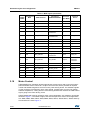
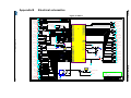
1
UM1871
User manual
Evaluation board with STM32F446ZE MCU
Introduction
The STM32446E-EVAL evaluation board has been designed as a complete demonstration
and development platform for the STMicroelectronics ARM® Cortex®-M4 with FPU core
based STM32F446ZET6 microcontroller with SPDIF input, four I2C, four SPI, three I2S, two
SAI, two CAN, three 12-bit ADC, two 12-bit DAC, up to 17 timers, USB OTG HS and FS,
camera interface, FMC and QuadSPI interfaces, SDIO interface, 512 KB Flash memory and
128KB SRAM, JTAG and ETM trace debugging support.The full range of hardware features
on the board can be used to evaluate all peripherals (USB HS & FS, USART, IrDA, CAN,
digital microphones, audio codec, ADC and DAC, color LCD glass with touchscreen,
SDRAM and QuadSPI Flash memories, I2C EEPROM, RF EEPROM, MicroSD card) and
develop user’s applications. Extension headers make it possible to easily connect a
daughter board specific application. An ST-LINK/V2-1 is integrated on the board, as
embedded in-circuit debugger and programmer for the STM32 MCU.
Figure 1. Figure 1: STM32446E-EVAL evaluation board
March 2015
DocID027604 Rev 1
1/64
www.st.com
1
Contents
UM1871
Contents
1
2
Overview . . . . . . . . . . . . . . . . . . . . . . . . . . . . . . . . . . . . . . . . . . . . . . . . . . 6
1.1
Features . . . . . . . . . . . . . . . . . . . . . . . . . . . . . . . . . . . . . . . . . . . . . . . . . . . 6
1.2
Demonstration software . . . . . . . . . . . . . . . . . . . . . . . . . . . . . . . . . . . . . . . 6
1.3
Order code . . . . . . . . . . . . . . . . . . . . . . . . . . . . . . . . . . . . . . . . . . . . . . . . . 7
1.4
Delivery recommendations . . . . . . . . . . . . . . . . . . . . . . . . . . . . . . . . . . . . . 7
Hardware Layout and configuration . . . . . . . . . . . . . . . . . . . . . . . . . . . . 8
2.1
3
2/64
Embedded ST_LINK/V2-1 . . . . . . . . . . . . . . . . . . . . . . . . . . . . . . . . . . . . . 9
2.1.1
Drivers . . . . . . . . . . . . . . . . . . . . . . . . . . . . . . . . . . . . . . . . . . . . . . . . . . 10
2.1.2
ST-LINK/V2-1 firmware upgrade . . . . . . . . . . . . . . . . . . . . . . . . . . . . . . 10
2.2
Power Supply . . . . . . . . . . . . . . . . . . . . . . . . . . . . . . . . . . . . . . . . . . . . . . .11
2.3
Clock Source . . . . . . . . . . . . . . . . . . . . . . . . . . . . . . . . . . . . . . . . . . . . . . 13
2.4
Reset Source . . . . . . . . . . . . . . . . . . . . . . . . . . . . . . . . . . . . . . . . . . . . . . 14
2.5
Boot Option . . . . . . . . . . . . . . . . . . . . . . . . . . . . . . . . . . . . . . . . . . . . . . . 15
2.6
Audio . . . . . . . . . . . . . . . . . . . . . . . . . . . . . . . . . . . . . . . . . . . . . . . . . . . . 16
2.7
USB OTG FS . . . . . . . . . . . . . . . . . . . . . . . . . . . . . . . . . . . . . . . . . . . . . . 18
2.8
USB OTG HS . . . . . . . . . . . . . . . . . . . . . . . . . . . . . . . . . . . . . . . . . . . . . . 19
2.9
RS232 and IrDA . . . . . . . . . . . . . . . . . . . . . . . . . . . . . . . . . . . . . . . . . . . . 19
2.10
MicroSD card . . . . . . . . . . . . . . . . . . . . . . . . . . . . . . . . . . . . . . . . . . . . . . 20
2.11
Potentiometer . . . . . . . . . . . . . . . . . . . . . . . . . . . . . . . . . . . . . . . . . . . . . . 20
2.12
Analog input or output . . . . . . . . . . . . . . . . . . . . . . . . . . . . . . . . . . . . . . . 21
2.13
CAN . . . . . . . . . . . . . . . . . . . . . . . . . . . . . . . . . . . . . . . . . . . . . . . . . . . . . 21
2.14
Memories . . . . . . . . . . . . . . . . . . . . . . . . . . . . . . . . . . . . . . . . . . . . . . . . . 22
2.15
RF-EEPROM . . . . . . . . . . . . . . . . . . . . . . . . . . . . . . . . . . . . . . . . . . . . . . 22
2.16
LCD Display and input devices . . . . . . . . . . . . . . . . . . . . . . . . . . . . . . . . 22
2.17
MFX (Multi Function eXpander) . . . . . . . . . . . . . . . . . . . . . . . . . . . . . . . . 23
2.18
Motor Control . . . . . . . . . . . . . . . . . . . . . . . . . . . . . . . . . . . . . . . . . . . . . . 24
Connectors . . . . . . . . . . . . . . . . . . . . . . . . . . . . . . . . . . . . . . . . . . . . . . . 26
3.1
Motor control connector CN3 . . . . . . . . . . . . . . . . . . . . . . . . . . . . . . . . . . 26
3.2
RF_Connectors CN6 and CN7 . . . . . . . . . . . . . . . . . . . . . . . . . . . . . . . . . 27
3.3
FMC_Connectors CN11 and CN12 . . . . . . . . . . . . . . . . . . . . . . . . . . . . . 28
DocID027604 Rev 1
UM1871
Contents
3.4
Daughterboard connector CN13 and CN10 . . . . . . . . . . . . . . . . . . . . . . . 30
3.5
MicroSD connector CN4 . . . . . . . . . . . . . . . . . . . . . . . . . . . . . . . . . . . . . . 31
3.6
RS232 connector CN25 . . . . . . . . . . . . . . . . . . . . . . . . . . . . . . . . . . . . . . 32
3.7
ST-LINK/V2-1 USB Type B connector CN16 . . . . . . . . . . . . . . . . . . . . . . 32
3.8
Audio jack CN22 and CN23 . . . . . . . . . . . . . . . . . . . . . . . . . . . . . . . . . . . 33
3.9
ST-LINK/V2-1 programming connector CN18 . . . . . . . . . . . . . . . . . . . . . 33
3.10
Power connector CN20 . . . . . . . . . . . . . . . . . . . . . . . . . . . . . . . . . . . . . . 33
3.11
Analog input connector CN21 . . . . . . . . . . . . . . . . . . . . . . . . . . . . . . . . . 34
Appendix A STM32446E-EVAL IO assignment. . . . . . . . . . . . . . . . . . . . . . . . . . . 35
Appendix B Electrical schematics . . . . . . . . . . . . . . . . . . . . . . . . . . . . . . . . . . . . 41
Appendix C Mechanical dimensions. . . . . . . . . . . . . . . . . . . . . . . . . . . . . . . . . . . 60
Appendix D Appendix D: Overview of FCC and IC regulations . . . . . . . . . . . . . 62
4
D.1
Part 15.19 . . . . . . . . . . . . . . . . . . . . . . . . . . . . . . . . . . . . . . . . . . . . . . . . . 62
D.2
Part 15.105 . . . . . . . . . . . . . . . . . . . . . . . . . . . . . . . . . . . . . . . . . . . . . . . . 62
D.3
Part 15.21 . . . . . . . . . . . . . . . . . . . . . . . . . . . . . . . . . . . . . . . . . . . . . . . . . 62
D.4
Industry Canada . . . . . . . . . . . . . . . . . . . . . . . . . . . . . . . . . . . . . . . . . . . . 62
Revision History . . . . . . . . . . . . . . . . . . . . . . . . . . . . . . . . . . . . . . . . . . . 63
DocID027604 Rev 1
3/64
3
List of tables
UM1871
List of tables
Table 1.
Table 2.
Table 3.
Table 4.
Table 5.
Table 6.
Table 7.
Table 8.
Table 9.
Table 10.
Table 11.
Table 12.
Table 13.
Table 14.
Table 15.
Table 16.
Table 17.
Table 18.
Table 19.
Table 20.
Table 21.
Table 22.
Table 23.
Table 24.
Table 25.
4/64
Power related jumpers and solder bridges . . . . . . . . . . . . . . . . . . . . . . . . . . . . . . . . . . . . . 11
32 KHz Crystal Y2 related Solder Bridges . . . . . . . . . . . . . . . . . . . . . . . . . . . . . . . . . . . . . 14
8 MHz Crystal Y4 related solder bridges . . . . . . . . . . . . . . . . . . . . . . . . . . . . . . . . . . . . . . 14
Boot0 switch . . . . . . . . . . . . . . . . . . . . . . . . . . . . . . . . . . . . . . . . . . . . . . . . . . . . . . . . . . . . 15
Boot0 & Boot1 Related Jumpers . . . . . . . . . . . . . . . . . . . . . . . . . . . . . . . . . . . . . . . . . . . . 15
Audio related jumpers . . . . . . . . . . . . . . . . . . . . . . . . . . . . . . . . . . . . . . . . . . . . . . . . . . . . . 17
USB_OTG_FS related jumpers . . . . . . . . . . . . . . . . . . . . . . . . . . . . . . . . . . . . . . . . . . . . . 18
RS232 & IrDA related jumpers . . . . . . . . . . . . . . . . . . . . . . . . . . . . . . . . . . . . . . . . . . . . . . 19
CAN related jumpers . . . . . . . . . . . . . . . . . . . . . . . . . . . . . . . . . . . . . . . . . . . . . . . . . . . . . 22
LCD modules . . . . . . . . . . . . . . . . . . . . . . . . . . . . . . . . . . . . . . . . . . . . . . . . . . . . . . . . . . . 23
MFX signals . . . . . . . . . . . . . . . . . . . . . . . . . . . . . . . . . . . . . . . . . . . . . . . . . . . . . . . . . . . . 23
Motor Control connector CN13 . . . . . . . . . . . . . . . . . . . . . . . . . . . . . . . . . . . . . . . . . . . . . . 26
Connector CN6 . . . . . . . . . . . . . . . . . . . . . . . . . . . . . . . . . . . . . . . . . . . . . . . . . . . . . . . . . . 27
Connector CN7 . . . . . . . . . . . . . . . . . . . . . . . . . . . . . . . . . . . . . . . . . . . . . . . . . . . . . . . . . . 27
FMC Connectors CN11 . . . . . . . . . . . . . . . . . . . . . . . . . . . . . . . . . . . . . . . . . . . . . . . . . . . 28
FMC Connectors CN12 . . . . . . . . . . . . . . . . . . . . . . . . . . . . . . . . . . . . . . . . . . . . . . . . . . . 29
DB_Connectors CN13 . . . . . . . . . . . . . . . . . . . . . . . . . . . . . . . . . . . . . . . . . . . . . . . . . . . . 30
DB_Connectors CN10 . . . . . . . . . . . . . . . . . . . . . . . . . . . . . . . . . . . . . . . . . . . . . . . . . . . . 31
MicroSD connector CN4 . . . . . . . . . . . . . . . . . . . . . . . . . . . . . . . . . . . . . . . . . . . . . . . . . . . 32
RS232 connector CN25 . . . . . . . . . . . . . . . . . . . . . . . . . . . . . . . . . . . . . . . . . . . . . . . . . . . 32
USB type B connector CN16 . . . . . . . . . . . . . . . . . . . . . . . . . . . . . . . . . . . . . . . . . . . . . . . 33
Analog input-output connector CN4 . . . . . . . . . . . . . . . . . . . . . . . . . . . . . . . . . . . . . . . . . . 34
IOs assignment . . . . . . . . . . . . . . . . . . . . . . . . . . . . . . . . . . . . . . . . . . . . . . . . . . . . . . . . . . 35
Mechanical dimension . . . . . . . . . . . . . . . . . . . . . . . . . . . . . . . . . . . . . . . . . . . . . . . . . . . . 61
Document Revision History . . . . . . . . . . . . . . . . . . . . . . . . . . . . . . . . . . . . . . . . . . . . . . . . 63
DocID027604 Rev 1
UM1871
List of figures
List of figures
Figure 1.
Figure 2.
Figure 3.
Figure 4.
Figure 5.
Figure 6.
Figure 7.
Figure 8.
Figure 9.
Figure 10.
Figure 11.
Figure 12.
Figure 13.
Figure 14.
Figure 15.
Figure 16.
Figure 17.
Figure 18.
Figure 19.
Figure 20.
Figure 21.
Figure 22.
Figure 23.
Figure 24.
Figure 25.
Figure 26.
Figure 27.
Figure 28.
Figure 29.
Figure 30.
Figure 31.
Figure 32.
Figure 33.
Figure 1: STM32446E-EVAL evaluation board. . . . . . . . . . . . . . . . . . . . . . . . . . . . . . . . . . . 1
Hardware Block Diagram . . . . . . . . . . . . . . . . . . . . . . . . . . . . . . . . . . . . . . . . . . . . . . . . . . . 8
STM32446E-EVAL evaluation board layout . . . . . . . . . . . . . . . . . . . . . . . . . . . . . . . . . . . . . 9
Updating the list of drivers in device manager . . . . . . . . . . . . . . . . . . . . . . . . . . . . . . . . . . 10
Solder bridge to be added on bottom side for Motor control. . . . . . . . . . . . . . . . . . . . . . . . 21
PCB underside rework for CAN . . . . . . . . . . . . . . . . . . . . . . . . . . . . . . . . . . . . . . . . . . . . . 22
PCB underside rework for Motor Control . . . . . . . . . . . . . . . . . . . . . . . . . . . . . . . . . . . . . . 25
Motor Control connector CN3 . . . . . . . . . . . . . . . . . . . . . . . . . . . . . . . . . . . . . . . . . . . . . . . 26
MicroSD connector CN4 (front view) . . . . . . . . . . . . . . . . . . . . . . . . . . . . . . . . . . . . . . . . . 31
RS232 connector CN25 (front view) . . . . . . . . . . . . . . . . . . . . . . . . . . . . . . . . . . . . . . . . . . 32
USB type B connector CN16 . . . . . . . . . . . . . . . . . . . . . . . . . . . . . . . . . . . . . . . . . . . . . . . 33
Power supply connector CN20 . . . . . . . . . . . . . . . . . . . . . . . . . . . . . . . . . . . . . . . . . . . . . . 34
Analog input-output connector CN21 . . . . . . . . . . . . . . . . . . . . . . . . . . . . . . . . . . . . . . . . . 34
MCU 1. . . . . . . . . . . . . . . . . . . . . . . . . . . . . . . . . . . . . . . . . . . . . . . . . . . . . . . . . . . . . . . . . 41
MCU 2. . . . . . . . . . . . . . . . . . . . . . . . . . . . . . . . . . . . . . . . . . . . . . . . . . . . . . . . . . . . . . . . . 42
Power . . . . . . . . . . . . . . . . . . . . . . . . . . . . . . . . . . . . . . . . . . . . . . . . . . . . . . . . . . . . . . . . . 43
USB OTG HS . . . . . . . . . . . . . . . . . . . . . . . . . . . . . . . . . . . . . . . . . . . . . . . . . . . . . . . . . . . 44
USB OTG FS . . . . . . . . . . . . . . . . . . . . . . . . . . . . . . . . . . . . . . . . . . . . . . . . . . . . . . . . . . . 45
ST-LINK/V2-1 . . . . . . . . . . . . . . . . . . . . . . . . . . . . . . . . . . . . . . . . . . . . . . . . . . . . . . . . . . . 46
MFX V3 . . . . . . . . . . . . . . . . . . . . . . . . . . . . . . . . . . . . . . . . . . . . . . . . . . . . . . . . . . . . . . . . 47
Peripherals . . . . . . . . . . . . . . . . . . . . . . . . . . . . . . . . . . . . . . . . . . . . . . . . . . . . . . . . . . . . . 48
CAN, RS232 / IrDA . . . . . . . . . . . . . . . . . . . . . . . . . . . . . . . . . . . . . . . . . . . . . . . . . . . . . . . 49
Audio. . . . . . . . . . . . . . . . . . . . . . . . . . . . . . . . . . . . . . . . . . . . . . . . . . . . . . . . . . . . . . . . . . 50
Memory . . . . . . . . . . . . . . . . . . . . . . . . . . . . . . . . . . . . . . . . . . . . . . . . . . . . . . . . . . . . . . . . 51
Motor Control . . . . . . . . . . . . . . . . . . . . . . . . . . . . . . . . . . . . . . . . . . . . . . . . . . . . . . . . . . . 52
STM32446E-EVAL LCD . . . . . . . . . . . . . . . . . . . . . . . . . . . . . . . . . . . . . . . . . . . . . . . . . . . 53
JTAG and trace. . . . . . . . . . . . . . . . . . . . . . . . . . . . . . . . . . . . . . . . . . . . . . . . . . . . . . . . . . 54
Camera connector . . . . . . . . . . . . . . . . . . . . . . . . . . . . . . . . . . . . . . . . . . . . . . . . . . . . . . . 55
Connectors . . . . . . . . . . . . . . . . . . . . . . . . . . . . . . . . . . . . . . . . . . . . . . . . . . . . . . . . . . . . . 56
FMC connectors . . . . . . . . . . . . . . . . . . . . . . . . . . . . . . . . . . . . . . . . . . . . . . . . . . . . . . . . . 57
3.2”LCD module with both SPI and 16bit interface . . . . . . . . . . . . . . . . . . . . . . . . . . . . . . . 58
Camera module . . . . . . . . . . . . . . . . . . . . . . . . . . . . . . . . . . . . . . . . . . . . . . . . . . . . . . . . . 59
Mechanical dimensions . . . . . . . . . . . . . . . . . . . . . . . . . . . . . . . . . . . . . . . . . . . . . . . . . . . 60
DocID027604 Rev 1
5/64
5
Overview
UM1871
1
Overview
1.1
Features
1.2
•
STM32F446ZET6 microcontroller.
•
3.2" 240x320 TFT color LCD with resistive touchscreen
•
2048 x 1536 camera module
•
SAI stereo audio DAC, audio jacks which support headset with microphone
•
Stereo digital microphones connected to DAC or to MCU
•
Connectors for microphone coupon board
•
SPDIF optical input connector
•
Joystick with 4-direction control and selector
•
Reset and user buttons
•
Potentiometer
•
4 color user LEDs
•
32MB QuadSPI Flash
•
4M x 16-bit SDRAM
•
2GB (or more) MicroSD card
•
RF-EEPROM
•
USB OTG HS and FS with micro-AB
•
Micro-AB connector
•
RS232 communication
•
CAN 2.0A/B compliant communication
•
IrDA transceiver
•
Embedded ST-LINK/V2-1
•
JTAG/SWD and ETM trace debug support
•
Five 5 V power supply options:
–
Power jack
–
ST-LINK USB connector
–
USB FS connector
–
USB HS connector
–
Daughter board
•
RTC with backup battery
•
Motor control connector
•
Extension connectors for daughter board or wrapping board and memory connectors
Demonstration software
Demonstration software is preloaded in the Flash memory of the board for easy
demonstration of the device peripherals in stand-alone mode. For more information and to
download the latest version available, refer to the STM32446E-EVAL demonstration
software available on the web: www.st.com.
6/64
DocID027604 Rev 1
UM1871
1.3
Overview
Order code
To order the evaluation board based on STM32F446ZE MCU, use the order code
STM32446E-EVAL.
1.4
Delivery recommendations
Before using the board for the first time, it must be verified that nothing was damaged during
shipment and that no components are unplugged or lost. When the board is extracted from
its plastic bag, it must be checked that no component remains in the bag.
The main components to verify are:
1.
The MicroSD card which may have been ejected from the CN4 connector (top left
corner of the board).
2.
The dual-interface EEPROM board (ANT7-M24LR-A) which may have been unplugged
from the CN1 connector (top left corner of the board).
Note:
The plastic protection on the camera should be removed carefully as the connection is very
fragile.
Note:
For all information concerning the version of the MCU used on the board, its specification
and possible related limitations, visit the ST web site (www.st.com) to download relevant
datasheet and errata sheet.
DocID027604 Rev 1
7/64
63
Hardware Layout and configuration
2
UM1871
Hardware Layout and configuration
The STM32446E-EVAL evaluation board is designed around the STM32F446ZET6
microcontroller in a 144-pin LQFP package. The hardware block diagram Figure 2 illustrates
the connection between STM32F446ZET6 and peripherals (Camera, RS232, Audio DAC,
microphone ADC, TFT LCD, CAN, IrDA, MicroSD card, RF E2PROM and others). Figure 3
will help the user to locate these features on the actual evaluation board.
Figure 2. Hardware Block Diagram
"!#
$$%
<+
$+
,
,
()*+%
12
!,
,
67
+89. 9
%9:+
, "34
.
4!,%+:
4!,
,
<
5
)
)!)=2
5
/
/
!,5
. 9(9
18$2+
;+
!<
,5
%
!,5
! ,
! ,
,
,5
8/64
!5
!
-.,/(0-&
& '
8
DocID027604 Rev 1
UM1871
Hardware Layout and configuration
Figure 3. STM32446E-EVAL evaluation board layout
CN
RF EEPROM
daughter board
connector
CN
63',)FRQQHFWRU
CN6,CN7,CN12,CN13
RF Connectors
CN3
Motor Control
connector
CN5
Camera
connector
U2
STM32F446ZET6
CN4
MicroSD card
CN
USB HS
connector
CN
CAN
CN
USB FS
connector
CN15
JTAG
connector
CN16
RS232
U10
IR receiver
CN17
LCD
connector
CN16
ST_LINK/V2-1
CN20
Power Jack
4 colors
LEDs
2.1
B1
Reset Button
B2
WKUP
Button
B3
Joystick
P2
$'&SRWHQWLRPHWHU
CN22
Audio1 jack
CN23
Audio2 jack
Embedded ST_LINK/V2-1
The ST-LINK/V2-1 programming and debugging tool is integrated on the STM32446E-EVAL
evaluation board.
The embedded ST-LINK/V2-1 supports only SWD for STM32 devices. For information about
debugging and programming features the user can refer to the User Manual UM1075 (STLINK/V2 in-circuit debugger/programmer for STM8 and STM32), which describes in detail
all the ST-LINK/V2 features.
DocID027604 Rev 1
9/64
63
Hardware Layout and configuration
UM1871
The changes versus ST-LINK/V2 version are listed below:
•
New features supported on ST-LINK/V2-1:
–
•
•
USB software re-enumeration
–
Virtual com port interface on USB
–
Mass storage interface on USB
–
USB power management request for more than 100 mA power on USB
Features not supported on ST-LINK/V2-1:
–
SWIM interface
–
Minimum supported application voltage limited to 3 V
Known limitation:
–
Activating the readout protection on ST-LINK/V2-1 target, prevents the target
application from running afterwards. The target readout protection must be kept
disabled on ST-LINK/V2-1 boards.
Note:
It is possible to power the board via CN16 (Embedded ST-LINK/V2-1 USB connector) even
if an external tools is connected to CN14 or CN15 (SWD connector).
2.1.1
Drivers
The ST-LINK/V2-1 requires a dedicated USB driver for Windows Vista 7 and 8, which can
be found on www.st.com. On Windows XP the ST-LINK/V2-1 driver requires WinUsb to be
installed, before using the ST-LINK/V2-1 (either available from Microsoft website or included
in the USB driver for ST-LINK/V2 for XP).
In case the STM32446E-EVAL evaluation board is connected to the PC before the driver is
installed, some STM32446E-EVAL interfaces may be declared as “Unknown” in the PC
device manager. In this case the user must install the driver files, and from the device
manager he must update the driver of the connected device.
Note:
Prefer using the “USB Composite Device” handle for a full recovery.
Figure 4. Updating the list of drivers in device manager
2.1.2
ST-LINK/V2-1 firmware upgrade
The ST-LINK/V2-1 embeds a firmware upgrade mechanism for in-situ upgrade through the
USB port. As the firmware may evolve during the life time of the ST-LINK/V2-1 product (for
example new functionalities, bug fixes, support for new microcontroller families), it is
10/64
DocID027604 Rev 1
UM1871
Hardware Layout and configuration
recommended to visit www.st.com, before starting to use the STM32446E-EVAL board and
periodically, in order to stay up-to-date with the latest firmware version.
2.2
Power Supply
STM32446E-EVAL evaluation board is designed to be powered by 5 V DC power supply
and to be protected by PolyZen from wrong power plug-in event. It is possible to configure
the evaluation board to use any of the following five sources for the power supply:
•
5 V DC power adapter connected to CN20 (PSU on silkscreen), the Power Jack on the
board. The external power supply is not provided with the board.
•
5 V DC power with 500 mA limitation from CN9, the USB_OTG_FS Micro-AB
connector
•
5 V DC power with 500 mA limitation from CN8, the USB_OTG_HS Micro-AB
connector
•
5 V DC power with 300 mA limitation from CN16, the ST-LINK/V2 USB
•
5 V DC power from both CN10 and CN12, the extension connector for daughterboard
The power supply is configured using JP12, JP21 and JP9 as described in Table 2: 32 KHz
Crystal Y2 related Solder Bridges.
Table 1. Power related jumpers and solder bridges
Jumper
JP12
Description
MCU_VDD is connected to 3.3 V power when JP12 is closed and MCU current
consumption measurement can be done manually by multi-meter when JP12 is open.
Default setting: Fitted.
To select the ST-LINK/V2-1 USB connector (CN16) power supply, set JP21 on U5V
position as shown (default setting):
,^
&^
ϱs
W^h
hϱs
JP21
06Y9
To select power supply jack (CN20 PSU) power supply, set JP21 on PSU as shown:
,^
&^
ϱs
W^h
hϱs
06Y9
DocID027604 Rev 1
11/64
63
Hardware Layout and configuration
UM1871
Table 1. Power related jumpers and solder bridges (continued)
Jumper
Description
To select daughterboard connector (CN10 and CN12) power supply, set JP21 on
D5V as shown:
,^
&^
ϱs
W^h
hϱs
06Y9
To select USB-OTG FS (CN9) power supply, set JP21 on FS as shown:
,^
&^
ϱs
W^h
hϱs
06Y9
JP21
To select USB-OTG HS (CN8) power supply, set JP21 on HS as shown:
,^
&^
ϱs
W^h
hϱs
06Y9
To select power supply jack (CN20) power supply to both STM32446E-EVAL and
daughterboard connected on CN10 and CN13, set JP21 on PSU and D5V as shown
(daughterboard must not have its own power supply connected)
,^
&^
ϱs
W^h
hϱs
06Y9
To connect MCU Vbat to 3.3 V power, set JP9 as shown (default setting):
1 2 3
JP9
To connect MCU Vbat to the battery, set JP9 as shown:
1 2 3
Note:
12/64
LED LD8 is lit when the STM32446E-EVAL evaluation board is powered by 5 V correctly.
DocID027604 Rev 1
UM1871
Hardware Layout and configuration
STM32446E-EVAL evaluation board can be powered from ST-LINK USB connector CN16
(U5V), but only ST-LINK part is powered before USB enumeration, because host PC only
provides 100 mA to the boards at that time. During the USB enumeration, STM32446EEVAL board asks for the 300 mA power to the Host PC. If the host is able to provide the
required power, the enumeration finishes by a “SetConfiguration” command and then, the
power transistor U11 (ST890) is switched ON, the red LED LD8 is turned ON, thus
STM32446E-EVAL board can consume maximum 300 mA current, but not more. If the host
is not able to provide such requested current, the enumeration fails, therefore the ST890
(U11) remains OFF and the 3.3 V part of the board will not be powered. As consequence,
the red LED LD8 remains turned OFF. In such case it is mandatory to use an external power
supply as extra power supply.
E5V (from PSU) or D5V can be used as external power supply, in case current consumption
of STM32446E-EVAL board exceeds the allowed current on USB. In this condition it is still
possible to use USB for communication for programming or debugging only, but it is
mandatory to power the board first using E5V or D5V, then connect the USB cable to the
PC. Proceeding in this way, ensures that the enumeration succeeds thanks to the external
power source.
The following power sequence procedure must be respected:
1.
Connect jumper JP21 for PSU or D5V side
2.
Check that JP18 is removed (PWR_EXT)
3.
Connect the external power source to CN20 (PSU) or D5V (daughterboard mounted)
4.
Check red LED LD8 is turned ON
5.
Connect the PC to USB connector CN16
If this order is not respected, the board may be powered by VBUS first, then E5V or D5V,
and the following risks may be encountered:
1.
If more than 300 mA current is needed by the board, the PC may be damaged or
current can be limited by PC. As a consequence the board is not powered correctly.
2.
300 mA will be requested at enumeration (since JP18 must be OFF), so there is risk
that request is rejected and enumeration does not succeed, if PC can’t provide such
current. Consequently the board is not powered (LED LD8 remains OFF).
Note:
In case the board is powered by an USB charger, there is no USB enumeration, so the led
LD8 remains set to OFF permanently and the board is not powered. Only in this specific
case the jumper JP18 needs to be set to ON, to allow the board to be powered anyway.
Note:
When the board is powered by ST-Link, the current is limited by U11 and the LED LD11 is
turned ON in case of over current detection.
2.3
Clock Source
Two clock sources are available on STM32446E-EVAL evaluation board for
STM32F446ZET6 and RTC embedded (see Table 2: 32 KHz Crystal Y2 related Solder
Bridges and Table 3: 8 MHz Crystal Y4 related solder bridges):
•
Y2, 32KHz Crystal for embedded RTC
•
Y4, 8MHz Crystal with socket for STM32F446ZET6 Microcontroller, Y3, 24MHz Crystal
for USB OTG HS.
•
Y5, 8MHz Crystal for ST_LINK.
DocID027604 Rev 1
13/64
63
Hardware Layout and configuration
UM1871
Table 2. 32 KHz Crystal Y2 related Solder Bridges
Solder bridge
Description
PC14 is connected to 32KHz crystal when SB108 is open (default setting).
SB108
PC14 is connected to DB_CONNECTOR CN13 when SB108 is closed. In such case
SB43 must be removed to avoid disturbance due to the 32 Khz quartz
PC15 is connected to 32KHz crystal when SB107 is open (default setting).
SB107
PC15 is connected to extension connector CN13 when SB107 is closed. In such
case SB56 must be removed to avoid disturbance due to the 32 Khz quartz
Table 3. 8 MHz Crystal Y4 related solder bridges
Solder bridge
Description
PH0 is connected to 8 MHz crystal when SB106 is open (default setting).
SB106
PH0 is connected to extension connector CN13 when SB106 is closed. In such case
SB69 must be removed to avoid disturbance due to the 32 Khz quartz.
PH1 is connected to 8 MHz crystal when SB105 is open (default setting).
SB105
PH1 is connected to extension connector CN26 when SB105 is closed. In such case
SB70 must be removed to avoid disturbance due to the 8 Mhz quartz.
2.4
Reset Source
The reset signal of STM32446E-EVAL evaluation board is low active and the reset sources
include:
Note:
14/64
•
Reset button B1
•
DB_Connectors from CN13 pin 13
•
Embedded ST-LINK/V2-1
•
RS232 connector CN25 pin 8 (CTS) for ISP.
The jumper JP5 should be set to control RESET by pin8 of RS232 connector CN25 (CTS
signal).
DocID027604 Rev 1
UM1871
2.5
Hardware Layout and configuration
Boot Option
The STM32446E-EVAL evaluation board is able to boot from:
•
Embedded User Flash
•
System memory with boot loader for ISP
•
Embedded SRAM for debugging
The BOOT0 option is configured by setting SW1.
Table 4. Boot0 switch
Switch
Description
STM32446E-EVAL boots from User Flash when SW1 is configured as shown
(default setting):
SW1
06Y9
STM32446E-EVAL boots from User RAM or System memory when SW1 is
configured as shown:
06Y9
BOOT0 can also be configured via RS232 connector CN25.
Table 5. Boot0 & Boot1 Related Jumpers
Jumper
Description
PB2 is used as ULPI_D4 (Camera interface) when JP22 is set as shown on the right
(default setting):
1 2 3
JP22
PB2 is used as BOOT1 and set at level 1 when JP22 is set as shown on the right:
1 2 3
DocID027604 Rev 1
15/64
63
Hardware Layout and configuration
UM1871
Table 5. Boot0 & Boot1 Related Jumpers (continued)
Jumper
Description
PB2 is used as BOOT1 and pulled down (level zero) when jumper is removed from
JP22 as shown on the right:
1 2 3
JP22
JP5
2.6
The Bootloader_BOOT0 is also managed by pin 6 of connector CN25 (RS232 DSR
signal) when JP5 is closed. This configuration is used for boot loader application
only. Default setting: Not fitted
Audio
An audio codec WM8994ECS/R with 4 DACs & 2ADCs inside, is connected to SAI interface
of STM32F446ZE, to support TDM feature on SAI port. This feature is able to implement
audio recording on digital Microphone & analog Microphone and audio playback of different
audio stream on headphones.
It communicates with STM32F446ZE via I2C4 bus which is shared with camera module,
RF-EEPROM & MFX (Multi Function eXpander).
The analog microphone on the headset is connected to ADC of WM8994ECS/R through
audio jack CN22. External speakers can be connected to WM8994ECS/R via audio jack
CN23.
Two Digital Microphones (MEMs microphone) MP34DT01TR are on STM32446E-EVAL
evaluation board. They can be connected to either audio codec or I2S port of STM32F446,
by setting jumpers as shown in Table 6: Audio related jumpers. The coupon connectors
CN26 & CN27 can be used to support MEMS microphone evaluation board STEVALMKI129V1, after removing SB1 & SB133.
An optical connector CN2 is implemented on STM32446E-EVAL, to receive external audio
data which is compatible with SPDIF spec.
16/64
DocID027604 Rev 1
UM1871
Hardware Layout and configuration
Table 6. Audio related jumpers
Jumper
Description
Data signal on digital microphone is connected to audio codec when JP20 is set as
shown on the right (default setting):
1 2 3
JP20
Data signal on digital microphone is connected to I2S port of STM32F446ZE when
JP20 is set as shown on the right:
1 2 3
Clock signal on digital microphone is connected to audio codec when JP19 is set as
shown on the right (default setting):
1 2 3
JP19
Clock signal on digital microphone is connected to Timer4 output (PD13) of
STM32F446ZE, used to divide by 2 the I2S3_CK, when JP19 is set, as shown on
the right (it is also needed to close SB23 & SB24 to use Timer 4 to manage
I2S3_CK):
1 2 3
Digital microphone power source is connected to +3.3V power when JP13 is set as
shown to the right (default setting):
1 2 3
JP13
Digital microphone power source is connected to MICBIAS1 from WM8994ECS/R
when JP13 is set as shown to the right:
1 2 3
Note:
I2C address of WM8994ECS/R is 0b0011010.
DocID027604 Rev 1
17/64
63
Hardware Layout and configuration
2.7
UM1871
USB OTG FS
STM32446E-EVAL evaluation board supports USB OTG full speed communication via a
USB Micro-AB connector (CN9) and USB power switch (U6) connected to VBUS. The
evaluation board can be powered by this USB connector (JP21 in position FS) at 5 V DC
with 500 mA current limitation. A green LED LD5 will be lit in two conditions:
•
STM32446E-EVAL works as an USB host and power switch (U6) is ON
•
STM32446E-EVAL works as a USB device if VBUS is powered by another USB host
A red LED LD5 will be lit when over-current is detected by the power switch U6.
Table 7. USB_OTG_FS related jumpers
Jumper
Description
STM32F446 port PA9 is used as USART1_TX (in conjunction with JP6) when JP7 is
set as shown below (see Warning):
4
1
2
3
STM32F446 port PA9 is connected to USB_FS_VBUS when JP7 is set as shown
below (see Warning):
JP7
4
1
2
3
STM32F446 port PA9 is connected to SPI when JP7 is set as shown below (see
Warning):
4
1
2
3
STM32F446 port PA10 is used as USART1_RX (in conjunction with JP8) when JP4
is set as shown below (see Warning):
1 2 3
JP4
STM32F446 port PA10 is connected to USB_FS_ID when JP4 is set as shown
below (see Warning):
1 2 3
18/64
DocID027604 Rev 1
UM1871
Hardware Layout and configuration
Warning:
2.8
There is an error on silkscreen of MB1162 PCB rev B:
- JP7 pin 1 is named SPI instead of UART
- JP7 pin 3 is named UART instead of SPI
USB OTG HS
STM32446E-EVAL evaluation board supports USB OTG high speed communication via a
USB Micro-AB connector (CN8) and USB HS PHY USB3300 (U4).The evaluation board can
be powered by this USB connector (CN8) at 5V DC with 500 mA current limitation. USB
power switch (U3) is connected on VBUS and provides power to CN8 (if SB131 is closed).
Green LED LD7 will be lit when either:
•
power switch (U3) is ON and STM32446E-EVAL works as a USB host
•
VBUS is powered by another USB host when STM32446E-EVAL works as an USB
device.
Red LED LD10 will be lit when over-current occurs.
JP22 should be configured as explained in Table 5: Boot0 & Boot1 Related Jumpers.
2.9
RS232 and IrDA
The RS232 transceiver U8 (with Hardware flow control CTS & RTS) connected to D-type 9pins RS232 connector CN25, and IrDA transceiver U10, are connected to USART1 of
STM32F446ZET6, which can be also shared with ST-LINK USART.
The signal Bootloader_RESET (shared with CTS signal) & Bootloader_BOOT0 (shared with
DSR signal) are added on RS232 connector CN8 for ISP support.
USART1 selection is done by setting JP6 and JP8, refer to Table 8: RS232 & IrDA related
jumpers for detail.
Table 8. RS232 & IrDA related jumpers
Jumper
Description
RS232_RX output of RS232 transceiver is connected to PA10 (USART1_RX in
conjunction with JP4), when JP8 is set as shown below (default setting):
1
3
5
JP8
2
4
6
IrDA_RX from IrDA transceiver is connected to PA10 (USART1_RX in conjunction
with JP4) when JP8 is set as shown below:
1
3
5
DocID027604 Rev 1
2
4
6
19/64
63
Hardware Layout and configuration
UM1871
Table 8. RS232 & IrDA related jumpers (continued)
Jumper
Description
USART_TX from ST-LINK is connected to PA10 (USART1_RX in conjunction with
JP4) to support virtual com port when JP8 is set as shown below:
1
3
5
JP8
2
4
6
RS232_TX input of RS232 transceiver is connected to PA9 (USART1_TX in
conjunction with JP7) when JP6 is set as shown below (default setting):
1 2 3
JP6
RS232_TX from ST-LINK is connected to PA9 (USART1_TX in conjunction with
JP7) to support virtual com port when JP6 is set as shown below:
1 2 3
2.10
MicroSD card
The 4GB (or more) MicroSD card is connected to SDIO interface of STM32F446ZET6.
MicroSD card detection is managed by MFX_IO15, configured with internal pull-up. The
following solder bridges are closed to support MicroSD card by default: SB26, SB27, SB28,
SB29, SB30, SB47.
2.11
Potentiometer
A 10 KΩ potentiometer P2 is connected to PA4 of the STM32F446ZET6 on the board.
The following solder bridges must be closed to connect potentiometer to PA4: SB91, SB92,
SB94, SB103. The potentiometer is not connected by default to PA4, since SB94, that is
marked in red in Figure 5, is opened to support Camera interface by default.
A low pass filter can be implemented, by replacing SB92 and C86 with the right value of
resistor and capacitor, as requested by end user’s application.
20/64
DocID027604 Rev 1
UM1871
Hardware Layout and configuration
Figure 5. Solder bridge to be added on bottom side for Motor control
2.12
Analog input or output
The analog input or output connector CN21 can be connected to PA4 of STM32F446ZET6,
used as ADC or DAC analog IO.
Solder bridge SB91 must be opened and SB92, SB94, SB103 must be closed to connect
CN21 to PA4. CN21 is not connected by default to PA4, since SB94 is opened to support
Camera interface by default.
In case CN21 is used as ADC, input low pass filter can be implemented by replacing SB92
and C86 with right value of resistor and capacitor, as requested by end user’s application. In
case CN21 is used as DAC output, a low pass filter can be implemented by replacing SB103
and C86 with the right value of resistor and capacitor, as requested by end user’s
application.
2.13
CAN
STM32446E-EVAL evaluation board supports one channels of CAN2.0 A/B compliant CAN
bus communication based on 3.3 V CAN transceiver. The High-speed mode, standby mode
and slope control mode are available and can be selected by setting JP2.
SB19, marked in red in Figure 6, must be closed to connect CAN1_RX to PB8. CAN1_RX is
not connected by default to PB8, since SB19 is open to support Camera interface by
default.
DocID027604 Rev 1
21/64
63
Hardware Layout and configuration
UM1871
Figure 6. PCB underside rework for CAN
Table 9. CAN related jumpers
Jumper
Description
CAN transceiver is working in standby mode when JP2 is set as shown to the right:
1 2 3
JP2
CAN transceiver is working in high-speed mode when JP2 is set as shown to the
right (default setting):
1 2 3
CAN transceiver is working in slope control mode when JP2 is open.
JP1
2.14
CAN terminal resistor is enabled when JP1 is fitted. Default setting: Not fitted
Memories
8M Bytes SDRAM is connected to SDRAM Bank1 of FMC interface of STM32F446ZE. All
signals for memory are also connected to extension connectors CN11 and CN12.
2.15
RF-EEPROM
An RF-EEPROM module ANT7-M24LR-A (MB1020A-02) is mounted on connector CN12
and connected to the common I2C4 bus of STM32F446ZET6. The I2C address of the RFEEPROM daughterboard is 0b1010000.
2.16
LCD Display and input devices
The 3.2” TFT color LCD connected to FMC bus and 4 general purpose color LEDs (LD 1, 2,
3, 4) are available as display devices. A touchscreen, a 4-direction joystick with selection
key and wakeup/tamper button (B2) are available as input devices and connected to MFX.
22/64
DocID027604 Rev 1
UM1871
Hardware Layout and configuration
Table 10. LCD modules
3.2” TFT LCD connector CN17
Pin
2.17
Description
Pin
connection
Pin
Description
Pin
connection
1
CS
FMC_NE1
18
PD14
FMC_D12
2
RS
FMC_A0
19
PD15
FMC_D13
3
WR/SCL
FMC_NWE
20
PD16
FMC_D14
4
RD
FMC_NOE
21
PD17
FMC_D15
5
RESET
RESET#
22
BL_VND
GND
6
PD1
FMC_D0
23
BL_Control
VDD
7
PD2
FMC_D1
24
VDD
+3V3
8
PD3
FMC_D2
25
VCI
+3V3
9
PD4
FMC_D3
26
GND
GND
10
PD5
FMC_D4
27
GND
GND
11
PD6
FMC_D5
28
BL_VDD
VDD
12
PD7
FMC_D6
29
SDO
NC
13
PD8
FMC_D7
30
SDI
NC
14
PD10
FMC_D8
31
XL
Touchscreen
X-
15
PD11
FMC_D9
32
XR
Touchscreen
X+
16
PD12
FMC_D10
33
YD
Touchscreen
Y-
17
PD13
FMC_D11
34
YU
Touchscreen
Y+
MFX (Multi Function eXpander)
The Multi Function eXpander (abbreviated MFX) is used on STM32446E-EVAL as IO
expander and as ADC inputs to manage the LCD touch screen. The communication
interface between MFX and STM32F446E is the common I2C4 bus.
Table 11. MFX signals
Pin
number
of MFX
Pin name of
MFX
3
PC14
MFX_GPO4
unused
Output
-
5
PH0
MFX_GPO5
LD2
Output
LED
6
PH1
MFX_GPO6
unused
Output
-
10
PA0
MFX_GPO0
Touch screen X+
ADC in
LCD
MFX functions
Function of
STM32756G-EVAL
DocID027604 Rev 1
Direction
Terminal
device
(For MFX)
23/64
63
Hardware Layout and configuration
UM1871
Table 11. MFX signals (continued)
2.18
Pin
number
of MFX
Pin name of
MFX
11
PA1
MFX_GPO1
Touch screen X-
ADC in
LCD
12
PA2
MFX_GPO2
Touch screen Y+
ADC in
LCD
13
PA3
MFX_GPO3
Touch screen Y-
ADC in
LCD
15
PA5
MFX_GPIO5
JOY_SEL
Input
Codec
16
PA6
MFX_GPIO6
OTG_FS_
OverCurrent
Input
USB_FS
17
PA7
MFX_GPIO7
OTG_FS_
PowerSwitchOn
Output
USB_FS
18
PB0
MFX_GPIO0
unused
-
-
19
PB1
MFX_GPIO1
JOY_RIGHT
Input
Joystick
20
PB2
MFX_GPIO2
JOY_LEFT
Input
Joystick
26
PB13
MFX_GPIO13
AUDIO_INT
Input
Audio Codec
27
PB14
MFX_GPIO14
unused
-
-
28
PB15
MFX_GPIO15
MicroSDcard Detect
Input
MicroSD
29
PA8
MFX_GPIO8
OTG_HS_
OverCurrent
Input
USB_HS
30
PA9
MFX_GPIO9
EXT_RESET
Output
CN1
Extension
connector
31
PA10
MFX_GPIO10
XSDN
Output
Camera
32
PA11
MFX_GPIO11
RSTI
Output
Camera
33
PA12
MFX_GPIO12
Camera_PLUG
Input
Camera
38
PA15
MFX_GPO7
LD4
Output
LED
39
PB3
MFX_GPIO3
JOY_DOWN
Input
Joystick
40
PB4
MFX_GPIO4
JOY_UP
Input
Joystick
MFX functions
Direction
Function of
STM32756G-EVAL
Terminal
device
(For MFX)
Motor Control
STM32446E-EVAL evaluation board supports both asynchronous and synchronous threephase brushless motor control via a 34 pins connector CN3, which provides all required
control and feedback signals to and from motor power-driving board. The available signals
on this connector are emergency stop, motor speed, 3 phase motor current, bus voltage,
heatsink temperature, coming from the motor driving board and 6 channels of PWM control
signal, going to the motor driving circuit.
Solder bridges that must be closed for motor control application, are marked in red and are
showed in Figure 7. The solder bridges, that must be opened for motor control application
are: SB85, SB83, SB84, SB19, SB46, SB26, SB38, SB114, SB110 SB111, SB112 and they
are showed in the same Figure 7.
24/64
DocID027604 Rev 1
UM1871
Hardware Layout and configuration
Figure 7. PCB underside rework for Motor Control
DocID027604 Rev 1
25/64
63
Connectors
UM1871
3
Connectors
3.1
Motor control connector CN3
Figure 8. Motor Control connector CN3
-36
Table 12. Motor Control connector CN13
Pin of
STM32F4x
Description
Pin
number
of CN3
Solder
bridge
Solder
bridge
Pin
number
of CN3
Pin of
STM32F4x
Description
Emergency STOP
PA6
1
-
-
2
-
GND
MC_UH
PC6
3
Close:
SB64
-
4
-
GND
MC_UL
PA5
5
Close:SB97 -
6
-
GND
MC_VH
PC7
7
Close:SB63 -
8
-
GND
MC_VL
PB0
9
Close:SB98 -
10
-
GND
MC_WH
PC8
11
Close:SB48 -
12
-
GND
MC_WL
PB1
13
Close:SB99 Close:SB59
14
PC0
BUS
VOLTAGE
CURRENT A
PA1
15
Close:SB87 -
16
-
GND
CURRENT B
PA2
17
Close:SB86 -
18
-
GND
CURRENT C
PA3
19
Close:SB74 -
20
-
GND
ICL Shut out
PG6
21
Close:
SB62
-
22
-
GND
DISSIPATIVE
BRAKE PWM
PD3
23
Close:
SB67
Close:SB72
24
PC2
Inductor
current
+5V power
-
25
-
Close:SB71
26
PC1
Heatsink
temperature
PFC SYNC
PA8
27
Close:SB49 -
28
-
3.3 V power
PFC PWM
PA11
29
Close:SB39 Close:SB52
30
PB12
PFC Shut
down
26/64
DocID027604 Rev 1
UM1871
Connectors
Table 12. Motor Control connector CN13 (continued)
Pin of
STM32F4x
Description
Pin
number
of CN3
Solder
bridge
Solder
bridge
Pin
number
of CN3
Pin of
STM32F4x
Description
Encoder A
PB6
31
Close:SB53 Close:SB73
32
PC3
PFC Vac
Encoder B
PB7
33
-
34
PB8
Encoder
Index
-
Note:
Some 0 Ohm resistors have to be removed or soldered to enable motor control application,
except the solder bridges configurations mentioned above.
3.2
RF_Connectors CN6 and CN7
Table 13. Connector CN6
Pin number
Signal Name
Pin number
Signal Name
1
RF_INT1
11
RF_SAI1_FS_A
2
I2C4_SDA
12
RF_SAI1_MCLK_A
3
I2C4_SCL
13
GND
4
GND
14
+3V3
5
RF_SPI2_MOSI/2_SD
15
SDCARD_CMD
6
RF_SPI2_SCK/2_CK
16
SDCARD_CK
7
RF_SPI2_MISO
17
SDCARD_D3
8
RF_SPI2_CS
18
SDCARD_D2
9
RF_SAI1_SCK_A
19
SDCARD_D1
10
RF_SAI1_SD_A
20
SDCARD_D0
Table 14. Connector CN7
Pin number
Signal Name
Pin number
Signal Name
1
GND
10
RF_USART6_CTS
2
RF_INT2
11
RF_USART6_TX
3
RF_VDDA
12
RF_USART6_RX
4
GND
13
RF_USART6_CK
5
RF_ADCb_12_IN5
14
RF_USART6_RTS
6
RF_ADCa_123_IN3
15
GND
DocID027604 Rev 1
27/64
63
Connectors
UM1871
Table 14. Connector CN7 (continued)
Pin number
3.3
Signal Name
Pin number
Signal Name
7
RF_TIM2_CH1/2_ETR
16
RF_SAI1_SD_B
8
RF_TIM2_CH2
17
+5V
9
RESET#
18
+3V3
FMC_Connectors CN11 and CN12
Table 15. FMC Connectors CN11
Pin number
28/64
Pin Name
Signal Name
1
GND
GND
2
+3V3
+3V3
3
PD14
FMC_D0
4
PD15
FMC_D1
5
PF4
FMC_D2
6
PD1
FMC_D3
7
GND
GND
8
GND
GND
9
PE7
FMC_D4
10
PE8
FMC_D5
11
PE9
FMC_D6
12
PE10
FMC_D7
13
PG6
QSPI_BK1_NCS
14
PF6
QSPI_BK1_IO3
15
PF9
QSPI_BK1_IO1
16
PD3
QSPI_CLK
17
PF7
QSPI_BK1_IO2
18
PF8
QSPI_BK1_IO0
19
PA7
FMC_SDNWE
20
PE0
FMC_NBL0
21
PF11
FMC_SDNRAS
22
PG15
FMC_SDNCAS
23
PG4
FMC_BA0
24
PC4
FMC_SDNE0
25
PG0
FMC_A10
26
PG5
FMC_BA1
DocID027604 Rev 1
UM1871
Connectors
Table 15. FMC Connectors CN11 (continued)
Pin number
Pin Name
Signal Name
27
PF1
FMC_A1
28
PF0
FMC_A0
29
PF3
FMC_A3
30
PF2
FMC_A2
31
GND
GND
32
+5V
+5V
Table 16. FMC Connectors CN12
Pin number
Pin Name
Signal Name
1
GND
GND
2
+3V3
+3V3
3
GND
GND
4
PD5
FMC_NWE
5
GND
GND
6
PD4
FMC_NOE
7
D5V
D5V
8
GND
GND
9
PD9
FMC_D14
10
PD10
FMC_D15
11
PE15
FMC_D12
12
PD8
FMC_D13
13
PE13
FMC_D10
14
PE14
FMC_D11
15
PE11
FMC_D8
16
PE12
FMC_D9
17
GND
GND
18
GND
GND
19
PE1
FMC_NBL1
20
PD7
FMC_NE1
21
PC5
FMC_SDCKE0
22
PG8
FMC_SDCLK
23
PG1
FMC_A11
DocID027604 Rev 1
29/64
63
Connectors
UM1871
Table 16. FMC Connectors CN12 (continued)
3.4
Pin number
Pin Name
Signal Name
24
PG2
FMC_A12
25
PF15
FMC_A9
26
PF14
FMC_A8
27
PF13
FMC_A7
28
PF12
FMC_A6
29
PF5
FMC_A5
30
PF4
FMC_A4
31
GND
GND
32
+5V
+5V
Daughterboard connector CN13 and CN10
Table 17. DB_Connectors CN13
Pin number
30/64
Signal Name
Pin number
Signal Name
1
GND
17
PC2
2
+3V3
18
PB1
3
PC13_ANTI_TAMP
19
VBAT
4
PA2
20
PB10
5
PC14_OSC32_IN
21
+5V
6
PA3
22
E5V
7
PC15_OSC32_OUT
23
GND
8
PA4
24
PB11
9
PH0_OSC_IN
25
PC3
10
PA6
26
PB12
11
PH1_OSC_OUT
27
PAO_WKUP
12
PA5
28
PB13
13
NRST
29
PA1
14
GND
30
PD11
15
PC0
31
+3V3
16
PB0
32
GND
DocID027604 Rev 1
UM1871
Connectors
Table 18. DB_Connectors CN10
Pin number
3.5
Signal Name
Pin number
Signal Name
1
D5V
17
PA11
2
+3V3
18
PB9
3
PD12
19
PA12
4
GND
20
GND
5
PD13
21
PA13
6
PB4
22
PC1
7
PG3
23
PA14
8
PB5
24
NC
9
PC6
25
PA15
10
PB7
26
PG11
11
P
27
PG9
12
BOOT0
28
PB3
13
PA10
29
PG10
14
NC
30
NC
15
GND
31
GND
16
PB8
32
+3V3
MicroSD connector CN4
Figure 9. MicroSD connector CN4 (front view)
DocID027604 Rev 1
31/64
63
Connectors
UM1871
Table 19. MicroSD connector CN4
Pin number
3.6
Description
Pin number
Description
1
SDCARD_D2(PC10)
5
SDCARD_CK (PC12)
2
SDCARD_D3(PC11)
6
VSS/GND
3
SDCARD_CMD(PD2)
7
SDCARD_D0(PC8)
4
+3V3
8
SDCARD_D1(PC9)
-
-
10
SDCARD_detect (mfx_io15)
RS232 connector CN25
Figure 10. RS232 connector CN25 (front view)
-36
Table 20. RS232 connector CN25
Pin number
3.7
Description
Pin number
Description
1
NC
6
RS232_DSR
2
RS232_RX
7
NC
3
RS232_TX
8
RS232_CTS
4
NC
9
NC
5
GND
-
-
ST-LINK/V2-1 USB Type B connector CN16
The USB connector CN16 is used to connect embedded ST-LINK/V2-1 to PC for debugging
of board.
32/64
DocID027604 Rev 1
UM1871
Connectors
Figure 11. USB type B connector CN16
Table 21. USB type B connector CN16
Pin number
3.8
Description
Pin number
Description
1
VBUS_STLINK (power)
4
GND
2
STL_USB_DM
5,6
Shield
3
STL_USB_DP
-
-
Audio jack CN22 and CN23
A 3.5mm Stereo audio jack CN22 and CN23 are connected to audio DAC and ADC is
available on STM32446E-EVAL board.
3.9
ST-LINK/V2-1 programming connector CN18
The connector CN18 is used only for embedded ST-LINK/V2-1 programming during board
manufacturing. It is not populated by default and not for end user.
3.10
Power connector CN20
STM32446E-EVAL evaluation board can be powered from a DC 5V power supply via the
external power supply jack (CN20) shown in Figure 10: RS232 connector CN25 (front view).
The central pin of CN20 must be positive.
DocID027604 Rev 1
33/64
63
Connectors
UM1871
Figure 12. Power supply connector CN20
'&9
*1'
-36
3.11
Analog input connector CN21
Figure 13. Analog input-output connector CN21
&1
$,1
06Y9
Table 22. Analog input-output connector CN4
Pin number
1
34/64
Description
GND
Pin number
2
DocID027604 Rev 1
Description
Analog input-output PA4
UM1871
STM32446E-EVAL IO assignment
Appendix A
STM32446E-EVAL IO assignment
LQFP144
Table 23. IOs assignment
Pin Name
Motor control
Default configuration
Camera
config
configuration
1
PE2
RF_SAI1_MCLK_A
TRACECLK
-
-
2
PE3
RF_SAI1_SD_B
TRACED0
-
-
3
PE4
RF_SAI1_FS_A
TRACED1
-
-
4
PE5
RF_SAI1_SCK_A
TRACED2
-
-
5
PE6
RF_SAI1_SD_A
TRACED3
-
-
6
VBAT
-
-
-
7
PC13ANTI_TAMP
Key TAMP_1 WKUP1
-
-
8
PC14OSC32_IN
-
-
-
9
PC15OSC32_OUT
-
-
-
10
PF0
FMC_A0
-
-
11
PF1
FMC_A1
-
-
12
PF2
FMC_A2
-
-
13
PF3
FMC_A3
-
-
14
PF4
FMC_A4
-
-
15
PF5
FMC_A5
-
-
16
VSS_5
-
-
-
17
VDD_5
-
-
-
18
PF6
QSPI_BK1_IO3
-
-
19
PF7
QSPI_BK1_IO2
-
-
20
PF8
QSPI_BK1_IO0
-
-
21
PF9
QSPI_BK1_IO1
-
-
22
PF10
RF_SPI2_CS
-
-
23
PH0 - OSC_IN
-
-
-
24
PH1 - OSC_OUT -
-
-
DocID027604 Rev 1
35/64
63
STM32446E-EVAL IO assignment
UM1871
LQFP144
Table 23. IOs assignment (continued)
36/64
Pin Name
Motor control
Default configuration
Camera
config
configuration
25
NRST
-
-
-
26
PC0
ULPI_STP
Bus_Voltage_ADC123_IN10
-
27
PC1
Mems_SPI3_MOSI
Heatsink_Temperature
_ADC123_IN12
-
28
PC2
ULPI_DIR
PFC_IndCurr_ADC123_IN12
-
29
PC3
ULPI_NXT
PFC_Vac_ADC123_IN13
-
30
VDD_12
-
-
-
31
VSSA
-
-
-
32
VREF+
-
-
-
33
VDDA
-
-
-
34
PA0-WKUP
MFX_IRQ_OUT
-
-
35
PA1
SAI2_MCLK_B
Current_ADC123_IN1
-
36
PA2
SAI2_SCK_B
Current_ADC123_IN2
-
37
PA3
ULPI_D0
RF_ADCa_123_IN3
Current_ADC123_IN3
-
38
VSS_4
-
-
-
39
VDD_4
-
-
-
40
PA4
ADC12_IN4
-
HSYNC
41
PA5
ULPI_CK
RF_ADCb_12_IN5
UL_TIM8_CH1N
42
PA6
-
STOP_TIM8_BKIN
PIXCLK
43
PA7
FMC_SDNWE
-
-
44
PC4
FMC_SDNE0
-
-
45
PC5
FMC_SDCKE0
-
-
46
PB0
ULPI_D1
VL_TIM8_CH2N
-
47
PB1
ULPI_D2
WL_TIM8_CH3N
-
48
PB2 / BOOT1
BOOT1 ULPI_D4
-
-
49
PF11
FMC_SDNRAS
-
-
50
PF12
FMC_A6
-
-
51
VSS_6
-
-
-
DocID027604 Rev 1
UM1871
STM32446E-EVAL IO assignment
LQFP144
Table 23. IOs assignment (continued)
Pin Name
Motor control
Default configuration
Camera
config
configuration
52
VDD_6
-
-
-
53
PF13
FMC_A7
-
-
54
PF14
FMC_A8
-
-
55
PF15
FMC_A9
-
-
56
PG0
FMC_A10
-
-
57
PG1
FMC_A11
-
-
58
PE7
FMC_D4
-
-
59
PE8
FMC_D5
-
-
60
PE9
FMC_D6
-
-
61
VSS_7
-
-
62
VDD_7
-
-
63
PE10
FMC_D7
-
-
64
PE11
FMC_D8
-
-
65
PE12
FMC_D9
-
-
66
PE13
FMC_D10
-
-
67
PE14
FMC_D11
-
-
68
PE15
FMC_D12
-
-
69
PB10
ULPI_D3
-
-
70
PB11
LD1
-
-
71
VCAP1
-
-
-
72
VDD_1
-
-
-
73
PB12
ULPI_D5
PFC_Shutdown_TIM1_BKIN
-
74
PB13
ULPI_D6
-
-
75
PB14
RF_SPI2_MISO
-
-
76
PB15
RF_SPI2_MOSI
-
-
77
PD8
FMC_D13
-
-
78
PD9
FMC_D14
-
-
79
PD10
FMC_D15
-
-
80
PD11
SAI_2_SD_A
-
-
81
PD12
I2C4_SCL
-
-
82
PD13
I2C4_SDA
-
-
DocID027604 Rev 1
37/64
63
STM32446E-EVAL IO assignment
UM1871
LQFP144
Table 23. IOs assignment (continued)
38/64
Pin Name
Motor control
Default configuration
Camera
config
configuration
83
VSS_8
-
-
-
84
VDD_8
-
-
-
85
PD14
FMC_D0
-
-
86
PD15
FMC_D1
-
-
87
PG2
FMC_A12
-
-
88
PG3
MFX_WAKEUP
-
-
89
PG4
FMC_BA0
-
-
90
PG5
FMC_BA1
-
-
91
PG6
QSPI_BK1_NCS
ICL_shutout_GPIO
-
92
PG7
RF_USART6_CK
-
-
93
PG8
FMC_SDCLK
-
-
94
VSS_9
-
-
-
95
VDD_1_USB33
-
-
-
96
PC6
-
UH_TIM8_CH1
D0
97
PC7
RF_USART6_RX
VH_TIM8_CH2
D1
98
PC8
SDCARD_D0
WH_TIM8_CH3
D2
99
PC9
SDCARD_D1
-
D3
100
PA8
RF_INT1
PFC_Sync_TIM1_CH1
-
101
PA9
USB_FS_VBUS
USART1_TX
RF_SPI2_SCK
-
-
102
PA10
USB_FS_ID
USART1_RX
-
-
103
PA11
USB_FS_DM
PFC_PWM_TIM1_CH4
-
104
PA12
USB_FS_DP
-
-
105
PA13
JTMS-SWDIO
-
-
106
VCAP2
-
-
-
107
VSS_2
-
-
-
108
VDD_2
-
-
-
109
PA14
JTCK-SWCLK
-
-
110
PA15
JTDI
-
-
111
PC10
SDCARD_D2
-
D8
DocID027604 Rev 1
UM1871
STM32446E-EVAL IO assignment
LQFP144
Table 23. IOs assignment (continued)
Pin Name
Motor control
Default configuration
Camera
config
configuration
112
PC11
SDCARD_D3
-
D4
113
PC12
SDCARD_CK
-
D9
114
PD0
FMC_D2
-
-
115
PD1
FMC_D3
-
-
116
PD2
SDCARD_CMD
-
D11
117
PD3
QSPI_CLK
Dissipative_brake_GPIO
D5
118
PD4
FMC_NOE
-
-
119
PD5
FMC_NWE
-
-
120
VSS_10
-
-
-
121
VDD_10
-
-
-
122
PD6
RF_INT2
-
D10
123
PD7
FMC_NE1 (CS_LCD)
-
-
124
PG9
SAI_2_FS_B
-
-
125
PG10
SAI_2_SD_B
-
-
126
PG11
SPDIF_RX0
-
-
127
PG12
RF_USART6_RTS
-
-
128
PG13
RF_USART6_CTS
-
-
129
PG14
RF_USART6_TX
-
-
130
VSS_11
-
-
-
131
VDD_11
-
-
-
132
PG15
FMC_SDNCAS
-
-
133
PB3
Mems_SPI3_SCK/3_CK
JTDO/TRACESWO
-
-
134
PB4
LD3 NJTRST
-
-
135
PB5
ULPI_D7
-
-
136
PB6
MIC_I2S_TIM4_CH1
EncA_TIM4_CH1
-
137
PB7
MIC_I2S_TIM4_CH2
EncA_TIM4_CH2
VSYNC
138
BOOT0
-
-
-
139
PB8
CAN_1_RX
RF_TIM2_CH1
EncIndex_TIM4_CH3
D6
140
PB9
CAN_1_TX
RF_TIM2_CH2
-
D7
DocID027604 Rev 1
39/64
63
STM32446E-EVAL IO assignment
UM1871
LQFP144
Table 23. IOs assignment (continued)
40/64
Pin Name
Motor control
Default configuration
Camera
config
configuration
141
PE0
FMC_NBL0
-
-
142
PE1
FMC_NBL1
-
-
143
PDR_ON
-
-
-
144
VDD_3
-
-
-
DocID027604 Rev 1
Electrical schematics
UM1871
Appendix B
Figure 14. MCU 1
SB83
SAI2_MCLKB
.
MFX_IRQ_OUT
CLOSE 0R
SB87
OPEN
SB86
MC_CurrentIN2
PA2
SB59
OPEN
SB84
SAI2_SCKB
PAO_WKUP
PA1
MC_CurrentIN1
MC_Bus_Voltage
OPEN
CLOSE 0R
SB94
SB112
ADC12_IN4
ULPI_STP
34
.
RF_ADCa_123_IN3
CLOSE 0R
MC_CurrentIN3
SB114
OPEN
ULPI_CK
CLOSE 0R
ULPI_D0
SB97
SB115
.
RF_INT1
SB96
PIXCLK
SB49
FMC_SDNWE
33R
SB11
CLOSE 0R
JTMS/SWDIO
USB_FS_ID
JTCK/SWCLK
JP4
3
2
1
JTDI
ULPI_D1
MC_VL
PC6
PA8
100
PA8
PC8
98
PC8
101
PA9
PC9
99
PC9
PA10
PC10
111
PC10
103
104
.
PA13
105
PA13
.
PA14
109
PA14
.
PA15
110
PA15
PB0
46
PB0
47
PB1
PB1
SB39
PC5
96
PC7
CLOSE 0R
MC_PFCpwm
45
PC6
PA7
102
SB113
USART1_RX
PC4
PA6
SB98
.
PC5
OPEN
I2S3_SD
R62
33R
SB72
MC_IndCurr
OPEN
33R
SB111
97
ULPI_DIR
PC7
CLOSE 0R
SB73
SB110
ULPI_NXT
CLOSE 0R
PA11
FMC_SDNE0
FMC_SDCKE0
SB64
PC11
PC12
112
PC11
113
PC12
MC_UH
OPEN
.
D0
SB46
RF_USART6_RX
OPEN
MC_VH
7
CLOSE 0R
R178
CLOSE 0R
48
PB2
32 1
PC14
OPEN
SB78
SB24
I2S3_CK
CLOSE 0R
CLOSE 0R
SB121
LD3
SB58
TRST
CLOSE 0R
OPEN
ULPI_D7
SB101
SB128
D5
CLOSE 0R
SB102
SB53
MC_EncA_CH1
OPEN
SB79
CLOSE 0R
134
PB5
135
PB6
136
PB7
137
PB8
139
PB9
140
PB10
69
PB11
70
PB12
73
CLOSE 0R
CLOSE 0R
SB21
MIC_TIM4_CH1
PB4
CLOSE 0R
.
PB13
74
PB14
75
SB20
MIC_TIM4_CH2
76
PB15
CLOSE 0R
.
SB116
VSYNC
25
NRST
CLOSE 0R
.
PC15_OSC32_OUT
C110
SB43
SB48
OPEN
PC15
PB4
MC_WH
2
.
D2
ABS07-32.768K-T
PB5
1
Y2
SB47
SB56
PB6
SDCARD_D1
PB7
CLOSE 0R
.
PB8
CLOSE 0R
C115
OPEN
.
D3
NOT FITTED
PB9
SB30
PB10
SDCARD_D2
CLOSE 0R
+3V3
.
PB11
PB12
D8
SB29
SDCARD_D3
PB13
PDR_ON
PB14
143
CLOSE 0R
R59
PDR_ON
.
10K
D4
SB28
PB15
SDCARD_CK
NRST
CLOSE 0R
.
D9
STM32F446ZET6
.
D6
PC14_OSC32_IN
9
OPEN
PB3
.
133
PB3
JTDO/SWO
8
CLOSE 0R
22-03-2031
SB37
OPEN
SB22
SDCARD_D0
CLOSE 0R
.
JP22
MC_WL
D1
SB26
NOT FITTED
PB2
47K
SB99
.
TAMPER_WKUP_KEY
SB109
.
SB100
ULPI_D2
OPEN
PC13_ANTI_TAMP
OPEN
ULPI_D4
CLOSE 0R
SB63
+3V3
PC13
.
RF_TIM2_CH1/2_ETR
SB19
OPEN
MC_EncIndex
.
SB50
OPEN
.
D7
JP5
1 2
SB18
3
CAN1_TX
B1
.
D3
1
.
OPEN
ULPI_D3
AF1-D-02-T/G
.
.
RF_TIM2_CH2
4
TD-0341
2
Bootloader_RESET
BAT60JFILM
List of changes between rev B-01 and B-02
LD1
SB85
CLOSE 0R
ULPI_D6
RF_SPI2_MISO
RESET#
- Y1 not fitted
- C110 & C115 not fitted
100nF
SB52
MC_PFC_Shutdown
.
C91
ULPI_D5
OPEN
CERAMIC CAPA (low esr)
Title:
Project:
41/64
Size:A3
RF_SPI2_MOSI/2_SD
Date:
MCU_1
STM32446E-EVAL
Reference: MB1162 Revision: B-02
11/03/15
Sheet: 1 of 17
life.augmented
Electrical schematics
CAN1_RX
MC_Vac
OPEN
PA12
CLOSE 0R
MC_EncA_CH2
MC_Heatsink
R63
OPEN
SB38
USB_FS_DM
.
DocID027604 Rev 1
22-03-2031
PC3
44
PA5
PA10
SB31
U2
PC2
29
41
PA11
AF2-D-06-G
.
JP7
1
PC4
28
SB71
43
PA12
USART1_TX
USB_FS_DP
PA4
PC1
42
PA9
RF_SPI2_SCK/2_CK
PC3
PC0
27
PA7
CLOSE 0R
4 2
3
PC2
PA3
CLOSE 0R
26
PA6
R64
OPEN
CLOSE 0R
USB_FS_VBUS
PA2
37
.
.
MC_PFCsync
10K
36
40
PA5
R80
PC1
PA3
OPEN
RF_ADCb_12_IN5
PC0
PA1
PA4
CLOSE 0R
MC_UL
STOP_TIM8_BKIN
PA0
35
SB74
.
HSYNC
.
OPEN
SB117
R57
FMC_NBL0
.
R58
SB76
SAI2_SDA
SB75
PD11
CLOSE 0R
SB77
33R
CLOSE 0R
PD13
77
R15
FMC_D1
R14 33R
PD5
PE5
PD6
PE6
PD7
PE7
PD8
PD11
PD12
86
PE9
PD10
81
85
PE8
PD9
80
82
FMC_D0
PE4
PE10
PE11
PE12
PD13
PD15
PE3
3
PE4
SB120
SB34
4
PE5
5
PE6
58
PE7
R38
59
PE8
R37 33R
FMC_D5
60
PE9
R36 33R
FMC_D6
33R
PE10
R35
64
PE11
R34 33R
FMC_D8
65
PE12
R28 33R
FMC_D9
PE13
67
PE14
R26
PE15
68
PE15
R25 33R
66
12
FMC_A3
R72 33R
13
FMC_A4
R73 33R
14
FMC_A5
R74 33R
15
.
.
.
.
.
33R
QSPI_BK1_IO3
18
19
QSPI_BK1_IO2
QSPI_BK1_IO0
20
QSPI_BK1_IO1
21
RF_SPI2_CS
22
R61
49
FMC_A6
R60 33R
50
FMC_A7
R52 33R
53
FMC_A8
R51 33R
54
FMC_A9
R50 33R
55
.
.
.
.
FMC_SDNRAS
R49
FMC_A11
R48 33R
FMC_A12
R13 33R
.
56
.
57
.
87
. PG3
MFX_WAKEUP
33R
R12
FMC_BA1
R1133R
88
89
.
FMC_BA0
.
90
TRACE_D2
RF_SAI1_SCK_A
CLOSE 0R
SB42
TRACE_D3
CLOSE 0R
FMC_D10
33R
RF_SAI1_FS_A
CLOSE 0R
CLOSE 0R
SB57
FMC_D11
RF_SAI1_SD_A
CLOSE 0R
FMC_D12
FMC_D[4-12]
BOOT0
.
2
1.
R68
10K
PF1
JP3
AF1-D-02-T/G
PF2
SW1
09 03290 01
PF3
PF4
1
Bootloader_BOOT0
.
+3V3
PF5
2
3
D2
BAT60JFILM
PF6
PF7
SB16
PF8
QSPI_BK1_NCS
CLOSE 0R
PF9
PF10
PG6
PF11
PG7
PF12
PG8
PF13
PG9
PF14
PG10
PF15
PG11
33R
FMC_A10
SB36
SB45
PG12
PG0
PG13
PG1
PG14
PG2
PG3
PG15
PG4
PH0
PG5
33R
PH1
91
SB62
MC_ICL
OPEN
92
93
RF_USART6_CK
PG8
R10
33R
.
R71 33R
138
SB44
FMC_D7
63
TRACE_D1
CLOSE 0R
124 PG9
SB61
125 PG10
SB60
PG11
SB25
FMC_SDCLK
SAI2_FSB
CLOSE 0R
126
SAI2_SDB
CLOSE 0R
SPDIF_RX0
CLOSE 0R
127
RF_USART6_RTS
33R
128
PG13
R45
129
PG14
.
FMC_A2
RF_SAI1_SD_B
CLOSE 0R
SB119
FMC_D4
PE14
BOOT0
PF0
TRACE_D0
CLOSE 0R
R46
33R
RF_USART6_TX
132
PG15
R47
.
11
.
10
R70 33R
.
33R
FMC_SDNCAS
23
24
PH0_OSC_IN
PH1_OSC_OUT
RF_USART6_CTS
C120
SB69
CLOSE 0R
20pF
Y4
STM32F446ZET6
SB70
8MHz
HC-49S-C16QSA-8M
C125
.
FMC_A[10-12]
.
DocID027604 Rev 1
R69
FMC_A1
RF_SAI1_MCLK_A
CLOSE 0R
33R
FMC_A0
TRACE_CLK
CLOSE 0R
SB17
R27 33R
PE13
PD14
33R
PE2
2
.
.
79
.
78
R16 33R
PD12
I2C4_SCL
CLOSE 0R
R17 33R
FMC_D15
PD4
1
.
R23
820R
R18
FMC_D14
PE3
.
R9
820R
FMC_D13
.
.
.
+3V3
.
33R
.
+3V3
123
.
D10
33R 122
R96
FMC_NE1
PE1
PE2
PD3
.
R33
PD6
.
U2
PD2
.
.
PD1
SB35
142 PE1
.
118
33R 119
.
R32
.
FMC_NWE
FMC_NBL1
141 PE0
.
117
PE0
PD0
.
33R 116
PD3
CLOSE 0R
RF_INT2
115
PD2
FMC_NOE
I2C4_SDA
114
33R
.
R31
.
OPEN
SB122
QSPI_CLK
R24
FMC_D3
.
SB67
MC_DissipativeBrake
FMC_D2
.
CLOSE 0R
33R
33R
.
SDCARD_CMD
.
FMC_D[13-15]
FMC_D[0-3]
SB27
.
.
D11
Electrical schematics
42/64
Figure 15. MCU 2
CLOSE 0R
20pF
Title:
Project:
Size:A3
Date:
MCU_2
STM32446E-EVAL
Reference: MB1162 Revision: B-02
11/03/15
Sheet: 2 of 17
life.augmented
UM1871
UM1871
Figure 16. Power
E5V
VDD_MCU
+3V3
D8
.1
1
2
2
GND
VIN
VOUT
3
B
.
B
3
FL3
BNX002-01
CB
CB
CG1
CG2
CG3
CN20
DC10B
2
1
ZEN056V130A24LS
.
D9
. SMAJ5.0A-TR
PSG
C53
100nF
PSG
1.
1.
C54
220uF
2
CG
JP12
AF1-D-02-T/G
2
+5V
U5V
+5V
TP8
.
REG1
LD1086D2M33TR
2
3
VOUT
VIN
4
.
D5V
VBUS_FS
VBUS_HS
TP16
.
+1V8
+3V3
REG3
LD1117S18TR
5001
3
2
VOUT 4
VIN
GND
. C51
100nF
JP21
TP19
.
5001
.
. C50
10uF
GND
C52
10uF
E5V
1
.
C55
10uF
2
3
6
5
4
7
TP17
.
5001
1
5001
8
1
9
10
A2-10-BSE
.
72
VDD_MCU
39
17
52
62
VDDA
84
TP7
.
5001
SB95
VREF+
144
CLOSE 0R
FL2
.
108
95
121
131
30
.
TP6
33
5001
32
VBAT
+3V3
6
VDD_1
VSS_2
VDD_2
VSS_4
VDD_3
VSS_5
VDD_4
VSS_6
VDD_5
VSS_7
VDD_6
VSS_8
VDD_7
VSS_9
VDD_8
U2
VDD1_USB33
VSS_10
VSS_11
VDD_10
VSSA
3
16
RED
LD8
19-213-R6C-AP1Q2B-3T
4
R107
120R
GND
1
51
61
.
C49
10uF
.
83
.
R108
150R
94
C48
10uF
120
130
31
VDD_11
VDD_12
VDDA
VREF+
VCAP_1
VCAP_2
VBAT
71
VDDA
VREF+
VDD_MCU
106
. C17
2.2uF
. C19
2.2uF
C27
1uF
2
JP9
2
VOUT
VIN
38
STM32F446ZET6
3
TP9
.
5001
REG2
LD1117STR
107
R151
1K
+2V8
POWER MCU
FCM1608KF-601T03
DocID027604 Rev 1
+5V
VDD_MCU
.
.
.
C123
100nF
C28
1uF
.
C121
100nF
C33
4.7uF
.
.
C18
4.7uF
1.
22-03-2031
+
POWER MCU
P1
-
CR1220_HOLDER
VDD_MCU
C112
100nF
.
C111
100nF
.
C116
100nF
.
C122
100nF
C113
100nF
.
C117
100nF
.
C124
100nF
.
C126
100nF
.
C127
100nF
.
C128
100nF
.
C129
100nF
POWER MCU
Title:
Project:
Size:A3
Date:
EVAL_POWER
STM32446E-EVAL
Reference: MB1162 Revision: B-02
11/03/15
Sheet: 3 of 17
life.augmented
43/64
Electrical schematics
.
.
+3V3
To MFX
SB139
OTG_HS_OverCurrent
MFX_IO8
+3V3
CLOSE 0R
.
R41
330R
.
R54
3.3K
LD10
R67
LD7
.
+5V
R56
12K
10K
CLKOUT
.
10K
VBUS_HS
PB10
ULPI_D3
19
20
DATA6
DP
DATA5
ID
DATA4
DATA3
VDD3_3_4
ULPI_D2
PB1
22
PB0
ULPI_D1
23
PA3
ULPI_D0
24
DATA2
U4
VDD3_3_3
DATA1
VDD3_3_2
DATA0
VDD3_3_1
27
R65
.
28
.
3
A2
7
B2
REG_EN
21
8
XO
XI
1M
VDD1_8_1
VDD1_8_2
VDDA1_8
5
RESET
GND1
GND2
GND3
.
C34
33pF
.
A2
A1
A2
A1
B2
B1
4
5
CIT1
ESDA14V2-2BF3
B2
31
B1
.
30
25
.
.
.
6
7
8
9
VBUS
DD+
ID
GND
GND
GND
GND
GND
SD475900001
16
6
15
+3V3
26
.
29
.
9
Y3
24MHz
XO75-YEGTC-24.000MHz
.
A1 CIT2
USBULC6-2F3
B1
EXC-3BP121H
PB2
ULPI_D4
1
C26
ULPI_D5
DM
C25
PB12
DATA7
100nF
18
B1
17
ULPI_D6
B2
ULPI_D7
PB13
A1
PB5
CN8
L1
EXC-3BP121H
820R
2
A2
1
2
.
C31
100nF
.
C30
100nF
C29
4.7uF
C32
4.7uF
..
C142
100nF
.
C140
100nF
C139
100nF
.
C141
100nF
33
C35
33pF
+3V3
.
R40
4.7K
R39
RESET#
.
DocID027604 Rev 1
ULP1_D[0-7]
VBUS
R55
E
R173
33R
4
T4
MMBT9013
B
.
.
.
R66
C
R43
47K
10
32
C23
4.7uF
3
L2
RBIAS
FAULT
2
C24
.
14
EXTVBUS
STP
GND
100nF
R53
PA5
ULPI_CK
DIR
EN
100nF
13
4
CLOSE 0R
3
C22
12
CPEN
100nF
PC2
PC0
SB130
NXT
SB131
ULPI_STP
11
STMPS2151STR
1
5 IN
OUT
U3
.
ULPI_DIR
PC3
19-21SYGC_S530-E2_TR8
CLOSE 0R
USB3300-EZK
ULPI_NXT
GREEN
620R
RED
19-213-R6C-AP1Q2B-3T
Electrical schematics
44/64
Figure 17. USB OTG HS
E
T3
MMBT9012
B
1K
C
.
R42
4.7K
Title:
Project:
Size:A3
Date:
USB_OTG_HS
STM32446E-EVAL
Reference: MB1162 Revision: B-02
11/03/15
Sheet: 4 of 17
life.augmented
UM1871
UM1871
Figure 18. USB OTG FS
+3V3
.
.
.
+5V
MFX_IO7
SB55
OTG_FS_PowerSwitchOn
5
.
4
C36
4.7uF
R81
R82
47K
620R
LD6
U6
STMPS2151STR
1
IN
OUT
EN
CLOSE 0R
GND
FAULT
RED
19-213-R6C-AP1Q2B-3T
3
MFX_IO6
OTG_FS_OverCurrent
2
R83
10K
TO MFX
VBUS_FS
CN9
1
VBUS
DD+
ID
GND
GND
GND
GND
GND
2
3
4
R85
DocID027604 Rev 1
USB_FS_DM
USB_FS_DP
USB_FS_ID
5
.
USB_FS_VBUS
PA11
10K
SB138
CLOSE 0R
SB137
CLOSE 0R
6
7
PA12
8
9
PA10
SD475900001
D-OUT
A2
DZ
A3
ID
B1
PD1
B2
PUP
B3
VBUS
D3
GND D2
D-IN D1
+3V3
D+OUT C3
PD2 C2
D+IN
.
C1
R87
330R
U7
EMIF02-USB03F2
LD5
GREEN
19-21SYGC_S530-E2_TR8
C
R84
.
B
47K
T5
MMBT9013
E
.
R172
10K
Project:
Size:A3
Date:
USB_OTG_FS
STM32446E-EVAL
Reference: MB1162 Revision: B-02
11/03/15
Sheet: 5 of 17
life.augmented
45/64
Electrical schematics
Title:
VBUS_HS
D13
+5V
+3V3_ST_LINK
+3V3_ST_LINK
.
BAT60JFILM
R115
VBUS_FS
.
R117
.
.
D7
2.7K
D12
4.7K
BAT60JFILM
.
. C95
100nF
.
2
1.
JP18
R114
C101
100nF
+3V3_ST_LINK
BAT60JFILM
E5V
D10
AF1-D-02-T/G
100K
USB_RENUMn
BAT60JFILM
+3V3_ST_LINK
D5V
POWER
D11
1 VIN
VIN
2 GND GND
3
INHIBIT
INHIBIT
U16
.
37
38
40
39
41
42
43
45
44
46
47
48
.
STM_JTCK_SWCLK
PWR_EXT
. C99
100nF
.
. C100
100nF
BAT60JFILM
VBUS_STLINK
R106
10K
+3V3_ST_LINK
OSCIN
SSL8000012AFDHF0-SJ28
HC-49XA-C20QQA-8.000MHz
OSC_OUT
STM_RST
+3V3
. C45
100nF
5
7
8
PA14
PB3
PB4
PA15
PB6
PB7
BOOT0
PB8
PB9
VSS3
PB5
PA11
VSSA
9
VDDA
11
12
.
C92
1uF
.
C93
100nF
31
PA9
30
29
28
PWR_ENn
T_JTMS
PB14
PB13
26
PB12
25
RED
JTDO/SWO
MCO
TP15
5001
R111
10K
OPEN
.
U11
1
.
T_JTCK
C88
4.7uF
IN
FAULT
IN
OUT
ON
OUT
GND
SET
2
8
R113
7
1K
5
ST890CDR
JTMS/SWDIO
U5V
6
3
4
JTCK/SWCLK
T_SWDIO_IN
LD11
19-213-R6C-AP1Q2B-3T
SB10
LED_STLINK
PA8
PA2
VBUS_STLINK
STL_USB_DM
T_SWO
PB15
PA1
VBUS_STLINK
STL_USB_DP
32
PA10
27
PA0_WKUP
C68
10nF
R118 .
2.7K
C94
100nF
.
VDD1
24
VSS1
PB11
PB10
21
22
23
PB2
20
PB1
PA7
PB0
19
17
18
SB15
T_JTDI
PA6
16
PA5
PA4
+3V3_ST_LINK
CLOSE 0R
JTCK/SWCLK
T_JTDO
ST_Link_RX
14
T_JTCK 15
2
1
.
RX
JP11
AF1-D-02-T/G
13
NOT FITTED
TX
PA3
ST_Link_TX
COM
LED_STLINK
.
T_NRST
JTDI
.
R101
100R
+3V3_ST_LINK
JTDO/SWO
R100
100R
+3V3_ST_LINK
RESET#
.
TRST
3
LD9
CN18
AF2-D-06-G
STM_JTMS_SWDIO
R112
100K
1
SWD
R171
100K
NOT FITTED
.
STM_JTCK_SWCLK
1.
2
3
4
HSMF-A201-A00J1
2
4
5
+3V3_ST_LINK
JP10
AF1-D-02-T/G
NOT FITTED
.
SB5
VBUS_STLINK
1
2
CLOSE 0R
+3V3_ST_LINK
.
USB STLINK
R110
10K
C
T6
MMBT9013
R102
.
R116
B
E
.
DocID027604 Rev 1
4.7K
R105
4.7K
.
U12
LD3985M33R
C70
100nF
STM_JTMS_SWDIO
33
STM32F103CBT6
NRST
10
34
PA12
OSCOUT
.
35
PA13
OSCIN
6
C69
1uF
VOUT
5
BYPASS
4
.
36
VSS2
OSC32OUT
R103
.
SB14
+3V3_ST_LINK
VBAT
OSC32IN
4
R104
100K
.
BAT60JFILM
VDD2
PC13_RTC
3
8MHz
.
OPEN
1.
2
Y5
.
.
+3V3_ST_LINK
.
VOUT
BYPASS
.
C47
20pF
.
.
C46
20pF
OPEN
.
SB33
VDD3
D14
Electrical schematics
46/64
Figure 19. ST-LINK/V2-1
100R
.
USB_RENUMn
R121
36K
1.5K
VBUS_STLINK
CN16
. 1
2
3
USB 4
5
6
67068-0000
SB4
CLOSE 0R
SB2
CLOSE 0R
STL_USB_DM
STL_USB_DP
Title:
Project:
Size:A3
Date:
ST_LINK/V2-1
STM32446E-EVAL
Reference: MB1162 Revision: B-02
11/03/15
Sheet: 6 of 17
life.augmented
UM1871
UM1871
Figure 20. MFX V3
+3V3
L5
EXC-3BP121H
+3V3
C72
100nF
+3V3
36
.
GPIO0
RESET#
GPIO1
.
SPARE
5001
GPIO2
18
TP13
19
D15
GPIO3
10
Touchscreen X+
20
JOY_LEFT
+3V3
Touchscreen Y+
aGPIO2
13
Touchscreen Y-
10K
NC
GPIO5
.
R128
GPIO6
U13
aGPIO3
GPIO7
STM32L152CCT6
44
GPIO8
BOOT0
510
7
GPIO10
40
JOY_UP
15
16
OTG_FS_OverCurrent
17 OTG_FS_PowerSwitchOn
29
OTG_HS_OverCurrent
SB12
2
+3V3
R135
47K
[NA]
MFX_SWDIO
MFX_SWCLK
34
PA0
SB13
37
46
CLOSE 0R
SB41
PD12
I2C4_SCL
+3V3
PD13
I2C4_SDA
CLOSE 0R
SB40
CLOSE 0R
SB32
GPIO12
SWDIO
1
MFX_IRQ_OUT
GPIO11
.
C114
100nF
MFX_IO8
EXT_RESET
31
XSDN
32
RST1
R127
47K
MFX_IO10
MFX_IO11
WAKEUP
.
CLOSE 0R
C98
100nF
MFX_IO7
42
43
45
GPIO13
SWLK
GPIO14
VLCD
GPIO15
Camera_PLUG
33
26
MFX_IO13
28
SD_CARD_DETECT
MFX_IO15
I2C_SCL
aGPIO5
I2C_SDA
aGPIO6
I2C_ADDR
aGPIO7
aGPIO4
.
.
5001
22
IDD_MEAS
MFX_V3
USART_RX
IDD_MCU
5001
R137
5
23
38
R138
LD3
3
LD3
19-213-R6C-AP1Q2B-3T
RED
680R
14
41
19-217-S2C-AM2N2VY-3T
ORANGE
TP14
TP18
5001
R124
LD4
19-217_BHC-ZL1M2RY_3T
BLUE
680R
VSSA
VSS_3
35 47
19-21SYGC_S530-E2_TR8
GREEN
LD2
680R
6
5001
VSS_1
TP11
USART_TX
VSS_2
TP12
LD1
390R
4
.
.
R130
10K
R136
LD1
IRQOUT
IDD_SH0
+3V3
.
27
OPEN
21
MFX_IO12
AUDIO_INT
.
PG3
.
MFX_IO6
30
NRST
MFX_WAKEUP
C104
100nF
JOY_SEL
.
DocID027604 Rev 1
GPIO9
JOY_DOWN
.
R139
GPIO4
aGPIO1
12
.
.
C71
100nF
aGPIO0
11
Touchscreen X-
39
.
BAT60JFILM
.
one capacitor close to each MFX pins:
VDD,VDD_1,VDD_2,VDD_3
JOY_RIGHT
.
TP10
25
5001
C103
100nF
JOYSTICK
VDDA
48
.
24
VDD_1
9
VDD_3
.
C80
1uF
VDD_2
.
8
CN19
AF2-D-06-G
MFX_SWCLK
1.
2
3
4
5
Title:
Project:
Size:A3
Date:
MFX_V3
STM32446E-EVAL
Reference: MB1162 Revision: B-02
11/03/15
Sheet: 7 of 17
life.augmented
47/64
Electrical schematics
+3V3
MFX_SWDIO
POTENTIOME7(5
Electrical schematics
48/64
Figure 21. Peripherals
WAKE_UP BUTTON
+3V3
+3V3
TWO PIN HEADER FOR EXTERNAL ANALOG INPUT / DAC OUTPUT
.
R150
CN21
.1
2
100R
AF1-D-02-T/G
4
R145
SB91
47R
CLOSE 0R
CLOSE 0R
.
3
C130
100nF
B2
C87
OPEN
TD-0341
NOT FITTED
2
1
C86
OPEN
R149
.
.
P2
3386P-103
2
.
SB92
CLOSE 0R
.
SB103
PA4
.
ADC12_IN4
3
1
ADC_potentiometer
TAMPER_WKUP_KEY
PC13-ANTI_TAMP
NOT FITTED
330R
.
CLOSE TO MCU ON PCB
R148
220K
DocID027604 Rev 1
+3V3
JOYSTICK
.
.
MICRO SD CARD
.
.
.
.
R131
R132
R129
NC
NC
NC
NC
NC
10K
10K
10K
R144
10K
10K
R143
.
.
R6
47K
B3
+3V3
.
+3V3
R7
47K
R8
47K
.
R21
47K
R20
47K
5 COMMON
2 CENTER
+3V3
4
CN4
TO MFX
JOY_SEL
JOY_LEFT
JOY_DOWN
JOY_RIGHT
JOY_UP
1
3
6
4
.
C81
NC
10nF
.
C82
NC
10nF
.
C83
NC
10nF
.
C85
NC
10nF
.
1
LEFT
DOWN
RIGHT
UP
6
3
MT-008A
SDCARD_D2
PC10
1
DAT2
GND
SDCARD_D3
PC11
2
CD/DAT3
GND
PD2
3
CMD
GND
SDCARD_CMD
SDCARD_CK
PC12
R22
10K
VDD
GND
5
CLK
SW1 10
SW2 9
C84
6
10nF
7
NC
.
4
VSS
DAT0
DAT1
11
SD_CARD_DETECT
PC9
8
MFX_IO15
SDCARD_D1
PJS0008-2000-1
PC8
Title:
Project:
Size:A3
Date:
SDCARD_D0
PERIPHERALS
STM32446E-EVAL
Reference: MB1162 Revision: B-02
11/03/15
Sheet: 8 of 17
life.augmented
UM1871
UM1871
Figure 22. CAN, RS232 / IrDA
JP2
22-03-2031
CAN
DEFAULT SETTING : 1<->2
+3V3
+3V3
1
. 2
3
R44
SB7
10K
CLOSE 0R
.
.
C90
100nF
U1
1.
6
CAN1_TX
1.
PB9
D
NC
8
2
7
GND
CANH
7
.1
2
Vcc
CANL
PB8
R
3
+3V3
8
DEFAULT SETTING : OPEN
.
6
SB3
R30
120R
3
CAN1_RX
JP1
AF1-D-02-T/G
2
CN24
LY-DR-M-001
4
9
5
OPEN
NC
4
5
2
1
10
D1
SN65HVD232D
11
ESDCAN24-2BLY
3
+3V3
C39
PA9
21
20
19
18
17
16
15
JP8
AF2-D-06-G
USART1_RX
PA10
2
3
4
5
6
VCC
C1-
GND
C2+
23
ST_Link_TX
26
25
27
3
V+
C2-
14 T1IN
13 T2IN
12 T3IN
RS232
USART1_TX
C1+
V-
C37
.
100nF 28
24
1
100nF 2
C40
9
10
11
T1OUT
T2OUT
T3OUT
100nF
.
.
C38
ST_Link_RX
1.
. C89
100nF
U8
JP6
1 2 3 22-03-2031
.
DocID027604 Rev 1
RS232 / IRDA
100nF
TXD
+3V3
R1OUTB
R2OUTB
R1OUT
R1IN
R2OUT
R2IN
R3OUT
R3IN
R4OUT
R5OUT
nEN
R4IN
R5IN
nSHDN
4
5
6
7
8
22
ST3241EBPR
1 .
DSR
6
2
RXD
CTS
7
3
8
4
CN25
LY-DR-M-001
RS232 CONNECTOR
9
5
Bootloader_BOOT0
U10
10
TFDU6300
Bootloader_RESET
5
+3V3
3
4
. R95
5.1R
.
R99
47R
1
2
6
7
8
SD
11
TxD
RxD
Anode(VCC2)
Cathode
VCC1
NC
GND
C44
4.7uF
.
C42
100nF
.
.
C43
4.7uF
C41
100nF
Title:
Project:
Size:A3
Date:
CAN / RS232_IRDA
STM32446E-EVAL
Reference: MB1162 Revision: B-02
11/03/15
Sheet: 9 of 17
life.augmented
49/64
Electrical schematics
.
+3V3
D9
+1V8
B2
PB3
SB23
D8
+3V3
G9
F1
D2
PB6
D4
10K
D5
C62
C65
.
.R170
C60
E6
PA2
G1
SAI2_FSB
PG9
E3
PG10
E4
PD11
F2
.
SAI2_SDA
1
3
AUDIO_INT
MFX_IO13
JP19
22-03-2031
2
SPKVDD2
SPKGND1
AVDD2
SPKGND2
CPVDD
CPGND
DCVDD
DGND
DBVDD
HP2GND
LDC2VDD
SCLK
SAI2_SCKB
SAI2_SDB
MIC_CLK
AGND3
+3V3
C6
PB7
AGND2
.
1uF
C67
4.7uF
.
4.7uF
.
100nF
C64
C131
C135
.
1uF
MIC_TIM4_CH2
AGND1
AVDD1
SPKVDD1
SDA
.
100nF
C134
.
1uF
.
100nF
.
4.7uF
100nF
.
C132
D1
C133
MIC_TIM4_CH1
C2
CLOSE 0R
I2S3_CK
LDO1VDD
G3
U14
LDO1ENA
CS/ADDR
D6
E7
E8
A1
C1
H9
E2
+3V3
F7
F3
H1
G2
CIFMODE
VREFC
MCLK1
BCLK1
GPIO2MCLK2
SPKMODE
LRCLK1
REFGND
DACDAT1
ADCDAT1
MICBIAS1
ADCLRCLK1
MICBIAS2
D3
H2
GPIO3BCLK2
F4
GPIO4LCLK2
G4
GPIO6LRCK2
E5
GPIO7ADAT2
H3
GPIO6DDAT2
VMIDC
A5
A7
R140
B6
C9
2.2K
C66
4.7uF
. R133
10K
.
C78
100nF
C74
U17
LEFT
MIC_VDD
DOUT
CLK
H5
GPIO10LCK3
H4
GPIO8DDAT3
F5
GPIO9ADAT3
C8
D7
IN1LN
VDD
GND
LR
1 VDD
2
LR
.
1
2
3
IN2LP/VRXN
B9
IN2RNDDAT1
SB1 MIC_DATA
PC1
I2S3_SD
C7
G6
HPOUT1L
H6
LINEOUT1N
C5
LINEOUT1P
B5
LINEOUT2N
C4
LINEOUT2P
B4
LINEOUTFB
A6
SPKOUTLN
B1
A2
SPKOUTLP
B7
SPKOUTRN
IN1RN
Time slot of SAI
A9
.
C61
. 100nF
C59
. 100nF
R123
20R
R122
20R
.
R146
1K
C76
C3
B3
C77
4.7uF
IN2RNDDAT2
CPCA
CPCB
CPVOUTP
JP13
CN22
PJ3028B-3
IN2RP/VRXP
+3V3
22-03-2031
6
3
4.7uF
SPKOUTRP
A8
OPEN
R147
SB125
180R
CLOSE 0R
IN1RP
CLOSE 0R
C79
100nF
G5
HPOUT1R
.
IN1LP
B8
HPOUT1FB
SB93
C75
4.7uF
2
4
.
3
GND1 5
GND2 6
7
GND3
GND4 8
CLK
GPIO11BCK3
1uF
MP34DT01TR
DOUT 4
.
JP20
22-03-2031
F6
F8
.
C73
4.7uF
.
LR
F9
HPOUT2P
.
.
LR
VDD
HPOUT2N
G8
G7
3
WM8994
2
CPVOUTN
. C57
2.2uF
H8
H7
C56
.
GND
1
2
GND1 5
GND2 6
7
GND3
GND4 8
CLK
VDD
SAI2_MCLKB
E1
A3
C58
.
SB133
CLOSE 0R
DocID027604 Rev 1
DOUT
PA1
A4
DMICCLK
MP34DT01TR
3
I2C4_SCL
OPEN
LDO2ENA
U15
RIGHT
CLK
I2C4_SDA
PD13
SB104
.
DOUT 4
PD12
.
+1V8
.
+1V8
R141
2
180R
4
6
.
E9
+3V3
Electrical schematics
50/64
Figure 23. Audio
.
R142
1K
3
CN23
PJ3028B-3
2.2uF
SB126
2.2uF
CLOSE 0R
.
1
.
1
2
10K
1
MIC_VDD .
MIC_DATA
RIGHT
+3V3
3
Coupons connectors
AF1-D-03-T/G
3
CN27A
2
LEFT
.
1
DRL1111
CN26B
2
VOUT
3
.R134
2
RIGHT
CN2
AF1-D-03-T/G
MIC_CLK
GND
3
CN26A
VCC
AF1-D-03-T/G
1
PG11
AF1-D-03-T/G
MIC_CLK
MIC_DATA
3
2
MIC_VDD
1
CN27B
.
C97
100nF
.
.
SPDIF_RX0
C96
30pF
Title:
LEFT
Project:
CLOSE TO CONNECTOR LESS THAN 7MM
Size:A3
Date:
AUDIO
STM32446E-EVAL
Reference: MB1162 Revision: B-02
11/03/15
Sheet: 10 of 17
life.augmented
UM1871
SDRAM
UM1871
Figure 24. Memory
FMC_D8
FMC_D11
FMC_D10
FMC_D9
FMC_D12
FMC_D13
FMC_D14
FMC_D15
FMC_D1
FMC_D0
FMC_D2
FMC_D3
FMC_D4
FMC_D5
FMC_D6
FMC_D7
FMC_D[0-15]
+3V3
+3V3
U9
MT48LC4M16A2P-6A
7
PE7
8
9
PE8
10
PE9
11
12
PE10
13
14
FMC_NBL0
PE0
15
PA7
16
PG15
17
FMC_SDNRAS
PF11
18
FMC_SDNE0
PC4
19
FMC_BA0
PG4
20
FMC_BA1
PG5
21
PG0
22
PF0
23
PF1
24
PF2
25
PF3
26
FMC_A2
FMC_A1
FMC_A0
FMC_A3
27
FMC_A10
DocID027604 Rev 1
FMC_SDNWE
FMC_SDNCAS
AUTRE REF:
MT48LC16MA2P-6A
48
PE15
47
PE14
100nF
100nF
.
.
.
C105
.
C118
.
100nF
100nF
100nF
100nF
100nF
49
.
C106
PD8
C108
PD9
50
C109
6
PD1
.
51
C119
5
PD10
52
C107
PD0
53
46
45
PE13
44
PE12
43
42
PE11
41
40
39
PE1
38
PG8
FMC_SDCLK
37
PC5
FMC_SDCKE0
36
PG2
35
PG1
34
PF15
33
PF14
32
PF13
31
PF12
30
PF5
29
PF4
FMC_NBL1
28
FMC_A11
FMC_A12
4
54
FMC_A9
PD15
VSS
DQ15
VSSQ
DQ14
DQ13
VDDQ
DQ12
DQ11
VSSQ
DQ10
DQ9
VDDQ
DQ8
VSS
NC
DQMH
CLK
CKE
A12
A11
A9
A8
A7
A6
A5
A4
VSS
FMC_A7
FMC_A8
3
VDD
DQ0
VDDQ
DQ1
DQ2
VSSQ
DQ3
DQ4
VDDQ
DQ5
DQ6
VSSQ
DQ7
VDD
DQML
WE#
CAS#
RAS#
CS#
BAO
BA1
A10
A0
A1
A2
A3
VDD
FMC_A4
2
FMC_A5
FMC_A6
1
PD14
FMC_A[0-12]
+3V3
QUAD_SPI
.
R86
10K
R79
PF9
2
+3V3
8
S#
Vcc
.
7
DQ1
R75
HOLD#/DQ3
.
QSPI_BK1_IO1
1
PG6
.
QSPI_BK1_NCS
U5
N25Q256A13EF840E
33R
6
W#/Vpp/DQ2
C
33R
5
DQ0
EP
33R
R78
PF8
QSPI_BK1_IO3
C102
100nF
QSPI_CLK
QSPI_BK1_IO0
33R
9
Title:
Project:
Size:A3
Date:
MEMORY
STM32446E-EVAL
Reference: MB1162 Revision: B-02
11/03/15
Sheet: 11 of 17
life.augmented
51/64
Electrical schematics
Vss
PD3
.
4
R76
.
3
R77
.
QSPI_BK1_IO2
PF7
PF6
33R
Electrical schematics
52/64
Figure 25. Motor Control
+3V3
.
R3
3.3K
OPEN
.
PC6
MC_UH
C16
1nF
MC_VL
TP2
.
5001
PA1
.
MC_CurrentIN1
PWM_2L
11
PWM_3H
13
PWM_3L
17
19
MC_DissipativeBrake
SB80
GND
12
PHASE B CURRENT+
PHASE B CURRENT-
18
PHASE C CURRENT-
20
23
DISSIPATIVE BRAKE
PFC Inductor current
24
25
+5V POWER
Heatsink Temperature
26
27
PFC SYNC
29
31
33
GND
3.3V Power
PFC PWM
PFC Shut down
Encoder A
PFC Vac
Encoder B
Encoder Index
SB66
PC2
28
.
SB54
OPEN
C8
OPEN
PC1
.
+3V3
30
32
MC_Heatsink
C9
100nF
R1
3.3K
34
.
PB12
.
C3
OPEN
MC_PFC_Shutdown
C7
1nF
.
SB51
C6
OPEN
C2
OPEN
PC3
MC_Vac
CLOSE 0R
.
C1
10nF
.
C5
OPEN
PB8
.
CLOSE 0R
C10
OPEN
C11
OPEN
SB65
CLOSE 0R
.
PA8
.
MC_PFCsync
MC_IndCurr
CLOSE 0R
22
HE10-34-MD
SB68
MC_Bus_Voltage
R2
100K
16
PHASE A CURRENT-
PHASE C CURRENT+
PC0
.
. C15
100nF
14
PHASE A CURRENT+
PD3
PB7
MC_EncA_CH2
GND
CLOSE 0R
ICL Shut out
PB6
MC_EncA_CH1
SB88
8
10
BUS VOLTAGE
+3V3
6
GND
21
PA11
CLOSE 0R
C12
OPEN
GND
CN3
PG6
+5V
C13 CLOSE 0R
OPEN
.
DocID027604 Rev 1
.
PWM_2H
CLOSE 0R
SB89
PA3
.
PWM_1L
7
15
MC_PFCpwm
MC_CurrentIN3
5
C14
OPEN
PA2
4
SB90
MC_ICL
MC_CurrentIN2
2
GND
9
PB1
MC_WL
GND
PWM_1H
PB0
PC8
MC_WH
EMERGENCY STOP
3
PC7
PA5
MC_UL
MC_VH
1
.
STOP_TIM8_BKIN
SB118
PA6
MC_EncIndex
C4
OPEN
Project:
MOTOR CONTROL
STM32446E-EVAL
Size:A3
Reference: MB1162 Revision: B-02
Title:
Date:
11/03/15
Sheet: 12 of 17
life.augmented
UM1871
UM1871
Figure 26. STM32446E-EVAL LCD
PD7
FMC_NE1
R152
.
PF0
FMC_A0
150R
.
PD5
FMC_NWE
CN17
R109
1.
150R
.
PD4
FMC_NOE
2
R169
3
150R
NRST
RESET#
4
5
6
.
150R
7
R160
R157
150R
8
FMC_D3
R158
150R
9
.
.
.
150R
FMC_D4
10
150R
R156
.
150R
11
FMC_D6
R153
.
150R
12
FMC_D7
R154
.
.
R155
FMC_D5
150R
13
.
.
.
150R
17
150R
18
150R
19
FMC_D11
R164
FMC_D12
R165
FMC_D13
R166
FMC_D14
R167
.
150R
150R
FMC_D15
R168
.
DocID027604 Rev 1
150R
150R
.
15
R163
.
14
R162
FMC_D10
.
R161
FMC_D9
FMC_D8
150R
HE14 2x17 DROIT FEMELLE
R159
FMC_D0
FMC_D1
FMC_D2
16
20
21
22
+3V3
23
24
25
26
27
28
FMC_D[0-15]
29
30
Touchscreen X-
L3
31
Touchscreen X+
32
Touchscreen Y-
33
Touchscreen Y+
34
EXC-3BP121H
+3V3
+5V
.
SB82
L4
CLOSE 0R
EXC-3BP121H
C138
100nF
C63
.
10uF
AF2-D-34-G
SB81
OPEN
Project:
Size:A3
Date:
EVAL_LCD
STM32446E-EVAL
Reference: MB1162 Revision: B-02
11/03/15
Sheet: 13 of 17
life.augmented
53/64
Electrical schematics
Title:
Electrical schematics
54/64
Figure 27. JTAG and trace
+3V3
.
R174
10K
NC
.
.
.
R175
10K
R176
10K
R177
10K
NC
NC
NC
+3V3
CN15
PA13
R88
PA14
R93
PB3
R89
JTDI
PA15
R90
TRST
PB4
R91
.1
2
22R
3
4
5
6
.
22R
.
JTDO/SWO
.
JTMS/SWDIO
JTCK/SWCLK
.
22R
.
22R
22R
7
8
9
10
R92
22R
11
+3V3
13
8
11
13
15
TRACE_D3
TRACE_D2
TRACE_D1
TRACE_D0
TRACE_CLK
17
18
19
20
.
SB127
.
R97
10K
R98
10K
12
14
.
16
18
19
20
PE5
+3V3
NC
10
17
PE6
14
16
OPEN
6
7
15
12
SB135
5
OPEN
4
R179
10K
OPEN
3
9
.
2
FTSH-110-01-L-DV
DocID027604 Rev 1
.1
SB134
CN14
HE10-20-MD
.
RESET#
R94
10K
D5
ESDALC6V1W5
1
5
2
4
3
D4
ESDALC6V1W5
1
5
2
4
3
PE4
PE3
PE2
D6
ESDALC6V1W5
1
5
2
4
3
Title:
Project:
Size:A3
Date:
Jtag and Trace
STM32446E-EVAL
Reference: MB1162 Revision: B-02
11/03/15
Sheet: 14 of 17
life.augmented
UM1871
CAMERA CONNNECTOR
+1V8
+1V8
+3V3
UM1871
Figure 28. Camera connector
C144
.
.
C143
TO MFX
OPEN
1
3
D10
5
D8
7
9
11
Camera_PLUG
I2C4_SCL_C
R125
2.2K
R126
MFX_IO10
XSDN
.
.
R119
10K
R120
10K
PC6
PC8
PC11
PB8
PA4
PA6
PIXCLK
+2V8
TP1 .
5001
D0
D2
D4
D6
2
4
6
8
10
12
14
16
18
20
22
15
17
2.2K
HSYNC
CN5
13
RST1
.
MFX_IO11
.
FROM MFX
SB123
MFX_IO12
OPEN
SB124
R4
10K
D10
D8
D6
PD6
D4
D2
D0
PC10
19
21
23
25
27
29
31
33
35
37
24
26
28
30
32
39
40
100nF
D11
D9
PD2
D11
D1
D3
PC12 D5
D7
D9
I2C4_SDA_C
5001
.
100nF
.
D1
D3
D5
D7
TP5
PC7
PC9
PB6
PB9
PB7
34
36
5001 .
38
5001
. C137
.
TP4
TP3
VSYNC
+2V8
.
100nF
CLM-120-02-L-D
C136
100nF
DocID027604 Rev 1
+1V8
+2V8
.
.
R19
4.7K
G
I2C4_SCL
PD12
VCC
1.
R5
4.7K
OE
OUT
GND
2
S
D
4
R29
10K
.
3
Y1
SM7745HEX-24.0M
NOT FITTED
I2C4_SCL_C
T1
BSN20
G
I2C4_SDA
PD13
S
D
I2C4_SDA_C
T2
BSN20
EXTRF E2P Connector
+3V3
+5V
1
2
I2C4_SCL
3
4
5
6
7
8
SB9
EXT_RESET
FROM MFX
CLOSE 0R
SB8
CLOSE 0R
CN1
SSM-104-L-DH
Title:
Project:
Size:A3
Date:
CAMERA_CONNECTOR
STM32446E-EVAL
Reference: MB1162 Revision: B-02
11/03/15
Sheet: 15 of 17
life.augmented
55/64
Electrical schematics
I2C4_SDA
+3V3
CN7
CN6
I2C4_SCL
RF_SPI2_MOSI/2_SD
RF_SPI2_MISO
RF_SAI1_SCK_A
RF_SAI1_FS_A
SDCARD_D3
SDCARD_D1
1
PD12
3
4
PB15
5
6
PB14
7
8
PE5
9
10
PE6
11
12
PE2
PE4
PD13
RF_SPI2_SCK/2_CK
PF10
13
14
PD2
15
16
PC12
PC11
17
18
PC10
PC9
19
20
PC8
1
2
3
4
PA5
5
6
PA3
PB8
7
8
PB9
9
10
PG13
PG14
11
12
PC7
PG7
13
14
PG12
15
16
PE3
17
18
I2C4_SDA
RF_ADCb_12_IN5
RF_TIM2_CH1/2_ETR
RF_SPI2_CS
RESET#
RF_SAI1_SD_A
RF_USART6_TX
RF_SAI1_MCLK_A
RF_USART6_CK
SDCARD_CK
SDCARD_D2
PD6
RF_INT2
RF_ADCa_123_IN3
RF_TIM2_CH2
RF_USART6_CTS
RF_USART6_RX
RF_USART6_RTS
RF_SAI1_SD_B
+3V3
SDCARD_CMD
RF_VDDA
2
PA8
+5V
RF_INT1
Electrical schematics
56/64
Figure 29. Connectors
SDCARD_D0
TSW-109-08-G-D
TSW-110-08-G-D
D5V
+3V3
+3V3
+5V
+3V3
E5V
CN13
PD12
PD13
PG3
PC6
PA9
PA10
PA11
PA12
PA13
2
3
4
5
6
7
8
9
10
11
12
13
14
15
16
17
18
19
20
21
22
23
24
25
26
PA14
PA15
27
28
29
30
31
32
PG9
PG10
PC13_ANTI_TAMP
close to MCU
DocID027604 Rev 1
CN10
.1
PB4
PB5
PB7
PC14_OSC32_IN
PC15_OSC32_OUT
PH0_OSC_IN
PH1_OSC_OUT
BOOT0
NRST
PC0
PB8
PC2
PB9
VBAT
PC1
PC3
PG11
PAO_WKUP
PB3
PA1
SB108
OPEN
SB107
OPEN
SB106
OPEN
SB105
OPEN
. 1
2
3
4
5
6
7
8
9
10
11
12
13
14
15
16
17
18
19
20
21
22
23
24
25
26
27
28
29
30
31
32
PA2
PA3
PA4
PA6
PA5
PB0
PB1
PB10
PB11
PB12
PB13
PD11
TSW-116-06-G-D
TSW-116-06-G-D
+3V3
.
RF_VDDA
FL1
FCM1608KF-601T03
C20
4.7uF .
C21
100nF
Title:
Project:
Size:A3
Date:
CONNECTORS
STM32446E-EVAL
Reference: MB1162 Revision: B-02
11/03/15
Sheet: 16 of 17
life.augmented
UM1871
UM1871
Figure 30. FMC connectors
D5V
+3V3
+3V3
FMC_CONNECTEUR
FMC_CONNECTEUR
1
FMC_D0
FMC_D2
CN11
1
2
4
PD15
5
6
PD1
7
8
PE7
9
10
PE8
PD0
3
FMC_D5
PE9
11
12
PE10
PG6
13
14
PF6
QSPI_BK1_IO1
PF9
15
16
PD3
QSPI_BK1_IO2
PF7
17
18
PF8
PA7
19
20
PE0
PF11
21
22
PG15
PG4
23
24
PC4
PG0
25
26
PG5
PF1
27
28
PF0
29
30
PF2
31
32
FMC_SDNWE
FMC_SDNRAS
FMC_BA0
FMC_A10
FMC_A1
FMC_A3
PF3
FTR-116-51-L-D
4
PD5
6
PD4
7
8
9
10
PD10
FMC_D7
QSPI_BK1_IO3
QSPI_CLK
FMC_D12
FMC_D10
PE15
11
12
PD8
PE13
13
FMC_D8
14
PE14
PE11
15
16
PE12
17
18
QSPI_BK1_IO0
FMC_NBL0
FMC_SDNCAS
FMC_SDNE0
FMC_BA1
FMC_A0
FMC_A2
FMC_NBL1
19
20
PD7
PD9
PE1
FMC_NWE
FMC_NOE
FMC_D13
PC5
21
22
PG8
FMC_A11
PG1
23
24
PG2
FMC_A9
PF15
25
26
PF14
PF13
27
28
PF12
PF5
29
30
PF4
31
32
FMC_SDCKE0
FMC_A7
FMC_A5
FMC_D15
FMC_D11
FMC_D9
FMC_NE1
FMC_SDCLK
FMC_A12
FMC_A8
FMC_A6
FMC_A4
+5V
FMC_D6
QSPI_BK1_NCS
2
5
FMC_D3
FMC_D14
CN12
3
FMC_D1
+5V
DocID027604 Rev 1
FMC_D4
PD14
FTR-116-51-L-D
Project:
Size:A3
Date:
FMC_CONNECTORS
STM32446E-EVAL
Reference: MB1162 Revision: B-02
11/03/15
Sheet: 17 of 17
life.augmented
57/64
Electrical schematics
Title:
2
3
4
CN1
CS
RS
WR
RD
#RESET
A
1
2
3
4
5
CS
RS
WR/SCL
RD
RESET
PD1
PD2
PD3
PD4
PD5
PD6
PD7
PD8
BLGND
BL_Control
VDD
BLVDD
SDO
SDI
22
23
24
25
26
27
28
29
30
PD10
PD11
PD12
PD13
PD14
PD15
PD16
PD17
BL_GND
BL_Control
VDD
VCI
GND
GND
BL_VDD
SDO
SDI
XL
XR
YD
YU
B
6
7
8
9
10
11
12
13
PD1
PD2
PD3
PD4
PD5
PD6
PD7
PD8
14
15
16
17
18
19
20
21
PD10
PD11
PD12
PD13
PD14
PD15
PD16
PD17
31
32
33
34
XL
XR
YD
YU
SDO
SDI
DocID027604 Rev 1
CS
WR
RD
RS
31
34
35
33
SDO
SDI
10
12
#RESET
32
VDD
A
K
C1
4.7uF/50V
STPS1L40M
U1
8
1
7
3
9
SW
Vo
Vi
NC
EN
GND
FB
PGND Rset
STLD40DPMR
BLGND
40
41
Z1
L1
BL_Control R5
0
36
37
38
39
11
4.7uH(1A)
BLGND
6
5
BLGND
44
43
6
42
45
1
VSYNC
HSYNC
DOTCLK
ENABLE
NC
CS
WR/SCL
RD
RS
SDO
SDI
RESET
VCC
VCC
LED_A
LED_K
VSS
VSS
VSS
VSS
IM1
IM3
IM0/ID
YU
YD
XR
XL
D0
D1
D2
D3
D4
D5
D6
D7
D8
D9
D10
D11
D12
D13
D14
D15
D16
D17
8
9
7
4K7
4K7
VDD
0
5
4
3
2
30
29
28
27
26
25
24
23
22
21
20
19
18
17
16
15
14
13
RP1
YU
YD
XR
XL
PD0
PD1
PD2
PD3
PD4
PD5
PD6
PD7
PD8
PD9
PD10
PD11
PD12
PD13
PD14
PD15
PD16
PD17
PD16
PD14
PD12
PD10
R6
100K
PD8
PD6
PD4
PD2
10K
RP3
PD9
PD0
RS
RD
10K
RP4
PD17
PD15
PD13
PD11
BLGND
HSYNC
Enable
VSYNC
DotClk
C
10K
RP5
R7
10
PD7
PD5
PD3
PD1
RP6
R8
do not fit
B
10K
RP2
FF0245SS1
AM-240320D4TOQW-T00H(R)
4
2
VDD
BLVDD
R2
R3
R4
VSYNC
HSYNC
DotClk
Enable
LCD board connector to Mother board
C
10K
Soldered for Serial interface only
The 34-pin connector to mother board for both
serial & 16bit interface. Compatible with
MB694 with Touch screen signals added on
Pin 31-34.
C2
2.2uF
R1
CN2
3.2LCD_connector
BLVDD
A
Soldered for i80-system 16-bit interface
Electrical schematics
58/64
Figure 31. 3.2”LCD module with both SPI and 16bit interface
1
10K
C3
1uF/50V
10K
D
D
STMicroelectronics
Title:
3.2" LCD module with both SPI & 16bit interface
Number:MB785
1
2
3
Rev: A.1(PCB.SCH)
Date: 3/27/2009
Sheet 1
of
1
4
UM1871
2
3
UM1871
Figure 32. Camera module
1
4
A
C5
+1V8
A
C6
CN2
100nF
+2V8
R9
22K
SCL
R12
STANDBY
CN1
Camera_CLK
PAR_PCLK
PAR_VSYNC
PAR_HSYNC
B
PAR_D0
PAR_D1
PAR_D2
PAR_D3
PAR_D4
PAR_D5
PAR_D6
PAR_D7
PAR_D[0..7]
DocID027604 Rev 1
+2V8
12
29
23
25
21
19
17
15
13
11
9
7
5
3
Camera_RST_S5K 22
24
STANDBY
R2
[N/A]
R3
[N/A]
SCL
SDA
18
20
+2V8
MCLK AVDD(2.8V)
PCLK
DVDD(1.8V)
VSYNC DOVDD(2.8V)
HSYNC
D0
D1
D2
D3
SHUTTER
D4
FLASH
D5
D6
D7
NC
D8
NC
D9
NC
NC
RESET
NC
PWDN
DGND
SCL
SDA
AGND
4
6
8
+2V8
+2V8
+2V8
C2
100nF
C1
100nF
0
R8
[N/A]
+1V8
C3
100nF
R10
[N/A]
R11
[N/A]
Camera_RST
PAR_D0
PAR_D2
PAR_D4
PAR_D6
PAR_HSYNC
PAR_PCLK
SHUTTER
R5
0
26 SHUTTER
14 FLASH
+2V8
C8
100nF
2
10
16
28
30
1
3
5
7
9
11
13
15
17
19
21
23
25
27
29
31
33
35
37
39
100nF
2
4
6
8
10
12
14
16
18
20
22
24
26
28
30
32
34
36
38
40
SDA
EXTCLK
PAR_D1
PAR_D3
PAR_D5
PAR_D7
PAR_VSYNC
B
FLASH
+2V8
FTMH-120-03-L-DV-ES
C7
100nF
PAR_D[0..7]
27
Camera Connector
1
AXE530124
+2V8
Camera Module :U866_3M_FF
SENSOR: S5K5CAGA
C
C
D1
BAT60JFILM
EXTCLK
Camera_RST
when mounted on big manta
board(MB10450), please soldered R6
10K and C9 470nF, removed R14 and
changed R13 with 0 ohm
4
1
R1
2K
R14
10K
3
2
SM7745HEW-24.0M
R6
10K[N/A]
Camera_RST_S5K
R13
10K
VCC OUT
EN
GND
Camera_CLK
[N/A]
U1
+2V8
R7
C4
100nF supply voltage: 2.5V+/-10%
BAT60 VF: 0.28@10mA
0.35@100mA
R4
0
default system clock using
clock from mother board.
C9
470nF[N/A]
D
D
STMicroelectronics
MB1183 Camera Module
Number:MB1183 Rev: C.1
1
2
3
Date: 1/27/2015
4
Sheet 1
of
1
59/64
Electrical schematics
Title:
Mechanical dimensions
Appendix C
UM1871
Mechanical dimensions
Figure 33. Mechanical dimensions
60/64
DocID027604 Rev 1
UM1871
Mechanical dimensions
Table 24. Mechanical dimension
Symbol
Size (mm)
Symbol
Size (mm)
Symbol
Size (mm)
X
124.33
A
55.88
E
11.88
Y
172.59
B
5.08
F
35.56
Lx
3.97
C
30.54
G
32.64
Ly
4.16
D
3.5
H
17
-
-
I
772.33
h
10
DocID027604 Rev 1
61/64
63
Appendix D: Overview of FCC and IC regulations
Appendix D
D.1
UM1871
Appendix D: Overview of FCC and IC
regulations
Part 15.19
This device complies with Part 15 of the FCC Rules. Operation is subject to the following
two conditions: (1) this device may not cause harmful interference, and (2) this device must
accept any interference received, including interference that may cause undesired
operation.
D.2
Part 15.105
This equipment has been tested and found to comply with the limits for a Class B digital
device, pursuant to part 15 of the FCC Rules. These limits are designed to provide
reasonable protection against harmful interference in a residential installation. This
equipment generates uses and can radiate radio frequency energy and, if not installed and
used in accordance with the instructions, may cause harmful interference to radio
communications. However, there is no guarantee that interference will not occur in a
particular installation. If this equipment does cause harmful interference to radio or
television reception, which can be determined by turning the equipment off and on, the user
is encouraged to try to correct the interference's by one or more of the following measures:
D.3
•
Reorient or relocate the receiving antenna.
•
Increase the separation between the equipment and the receiver.
•
Connect the equipment into an outlet on a circuit different from that to which the
receiver is connected.
•
Consult the dealer or an experienced radio/TV technician for help.
Part 15.21
Any changes or modifications to this equipment not expressly approved by
STMicroelectronics may cause, harmful interference and void the FCC authorization to
operate this equipment.
D.4
Industry Canada
This device complies with Industry Canada licence-exempt RSS standard(s). Operation is
subject to the following two conditions : (1) this device may not cause interference, and (2)
this device must accept any interference, including interference that may cause undesired
operation.
Le présent appareil est conforme aux CNR d’Industrie Canada applicables aux appareils
radio exempts de licence. L’exploitation est autorisée aux deux conditions suivantes : (1)
l’appareil ne doit pas produire de brouillage, et (2) l’utilisateur de l’appareil doit accepter tout
brouillage radioélectrique subi, même si le brouillage est susceptible d’en compromettre le
fonctionnement.
62/64
DocID027604 Rev 1
UM1871
4
Revision History
Revision History
Table 25. Document Revision History
Date
Version
23-Mar-2015
1
Revision Details
Initial Version
DocID027604 Rev 1
63/64
63
UM1871
IMPORTANT NOTICE – PLEASE READ CAREFULLY
STMicroelectronics NV and its subsidiaries (“ST”) reserve the right to make changes, corrections, enhancements, modifications, and
improvements to ST products and/or to this document at any time without notice. Purchasers should obtain the latest relevant information on
ST products before placing orders. ST products are sold pursuant to ST’s terms and conditions of sale in place at the time of order
acknowledgement.
Purchasers are solely responsible for the choice, selection, and use of ST products and ST assumes no liability for application assistance or
the design of Purchasers’ products.
No license, express or implied, to any intellectual property right is granted by ST herein.
Resale of ST products with provisions different from the information set forth herein shall void any warranty granted by ST for such product.
ST and the ST logo are trademarks of ST. All other product or service names are the property of their respective owners.
Information in this document supersedes and replaces information previously supplied in any prior versions of this document.
© 2015 STMicroelectronics – All rights reserved
64/64
DocID027604 Rev 1