1
Circuit Test Point Impedance
Knowing the source impedance at
the point of measurement is critical.
If the source impedance is low, rise
time and amplitude measurements
are generally no problem. For example, batteries and power supplies
h a v e source impedances of milliohms. Signal generators are 25, 50
or 600 ohms. The problem occurs
when the source impedance is high.
TTL h a s a source impedance of
-2.5kR so even a t very low frequencies (single shot), measuring fast
transition times is difficult a t best.
Basic Probe Considerations
If t h e scope is being used a s a
monitoring device, the connection
between the signal source and scope
is usually a direct 50R cable. However, if the scope is being used for
signal tracing or circuit analysis,
then some type of a n isolating device
must be used to prevent the scope
from loading the circuit and a t tenuating the signal. Today’s modern oscilloscopes use a probe for this
isolation.
The frequency of the signal you are
measuring and source impedance at
the point of measurement influences
which probe to use. What you want
to measure -rise time or amplitude
- is also a weighing factor. In general, there are four types of probes
available for common circuit
analysis.
- High resistance probes
- Miniature passive divider
- Active (FET)
- Current probes
Any voltage probe will load the circuit you are attempting to measure.
If amplitude measurements at low
frequencies a r e all you a r e interested in, then a passive one-toone 1MR non-attenuating probe
may be all you need. A good rule-ofthumb to remember is, “To keep resistive loading errors below 1%,
select a probelscope combination
that has an Rin that is a t least 100
times greater t h a n t h e source
impedance.”
But as frequencies rise, or pulse rise
time becomes very fast, scope input
capacitance becomes more and more
important, forcing use of an miniature passive divider probe to reduce
that input capacitance.
And a t the highest frequencies, if
both amplitude and rise time are
important in high source impedance
circuits, an active FET input probe
should be used.
If the ultimate in rise time is needed,
a 500 divider probe may be used.
However, you must be careful of DC
loading. A 50R divider probe with a n
input Xc of 5000 will attenuate the
amplitude of a signal, or upset the
bias of the circuit if you probe the
wrong point (e.g., collector of a transistor), or burn up the probe if you
draw too much current.
A current probe is useful in those
certain situations where touching
the circuit with any voltage probe a t
all, even one with t h e smallest
capacitance, changes the circuit’s
operation. It may be the collector of a
transistor where a n inductor and
capacitance form a tuned circuit.
Probe Rules for Making
Amplitude Measurements
If
have a
a
minimum impedance source. For
example : emitter-to-base impedance of a transistor is generally
lower than the collector-to-base
impedance (this implies a balanced input measurement).
2. Select a probe with the highest
possible Zin at the frequency of
interest. When measuring pulse
amplitude, capacitance is not as
important as Rin being high relative t o the source impedance.
WWW.HPARCHIVE.COM
While probe capacitance distorts
pulse shape, the flat portion of
the pulse top (maximum
amplitude) can be used to make
an accurate amplitude measurement since i t contains low frequency information. Conversely,
if the pulse width is small compared to the measurement system
rise time, input capacitance can
introduce errors since the source
cannot fully charge the input
capacitance during its on time.
This problem becomes worse with
increasing source impedance.
3. When source impedance is unknown, the probe with the highest Zin usually yields the greatest
accuracy. However, for frequencies above 10 MHz, high probe
capacitance can reduce accuracy
more than high probe resistance
can help.
4. If the source voltage is totally
unknown, it is wise to start with
a 1OO:l divider probe to reduce
the possibility of damaging the
probe. This will also indicate
whether or not there is enough
signal available t o capitalize on
the relatively low capacitance of
a 1OO:l divider probe. However,
in real-life situations, you probably don’t have a 1OO:l divider
probe. If this is the case use your
standard 1 O : l divider probe.
’7
Probe Rules for Making Rise
Time Measurements
1. Always try to probe the lowest
impedance point that contains
the waveform of interest. For
example: emitter-to-base impedance of a transistor is generally
lower than the collector-to-base
impedance (this implies a balanced input measurement).
2. The fastest input system will
generally have the lowest Rin
and Cin. (This rule is limited only
by the maximum resistive loading that the source can tolerate.)
3
c
3. A t high frequencies, the 50R divider probe (500R at lpf) is the
best bet for accurate rise time
measurements. However, you
must be careful of DC loading.
The 500Q input Xc will attenuate
the amplitude of a signal, or
upset the bias of the circuit if you
probe the wrong point (e.g., collector of a transistor), or burn up
the probe if you draw too much
current.
T I
n
m
. mee
- Aavice on
HOW 1.0 bet
.
1
.
Signal Source Loading and
Probes
Application Note 152, titled “Probing In Perspective,” is available
free of charge from Hewlett-Packard
(write to the address at the rear of
this issue). AN152 describes i n
detail all aspects of signal source
loading and probes. There a r e
graphs, formulas, and lots of good
information - much more than can
be briefly described here.
capabilities. If it doesn’t, select the
slowest sweep speed possible. This
will present a very slow-moving dot
which you can use for adjustments.
To adjust astigmatism and focus, set
the beam intensity to a low level.
Position the spot to center screen
and then adjust t h e focus and
astigmatism controls for the smallest round dot.
How many of you are guilty of picking up a divider probe, connecting it
to your scope and t a k i n g measurements without first checking the
probe’s compensation?
One of the most common “pilot errors” is using an un-compensated
probe to make measurements. An
un-compensated probe will cause errors in the display which will be undetected
Some kind Of a
standard waveform is checked. To be
safe, You should always check probe
compensation:
- at the beginning of each work
day
Probe Compensation and
Calibrating Your Scope
- whenever you re-connect a probe
After you have gone through the
rigors of selecting the right probe,
you’re ready to make some
measurements.
To compensate the probe, connect it
to the calibrator squarewave signal,
select DC coupling, and adjust the
scope’s controls for a stable display.
Select the lowest VOLTSLDIV setting possible and center the top portion of the squarewave on the screen.
This provides a more precise adjustment method (if your scope is adjusted properly). Adjust the probe
until you get a flat-topped square
wave with no rounding or overshoot
of the signal’s corners. Refer to
Figure 2.
Let’s begin by making sure your
scope is operating properly. You
should check its trace alignment
astigmatism and focus adjustments, and finally, if required, probe
compensation.
Trace alignment may be needed if
your scope is operated near a strong
magnetic field. To make this adjustment, ground the input and adjust the TRACE ALIGNMENT conthe best trace alignment
orizontal graticule line.
way to adjust astigmatism
is with a dot displayed on
m. Of course this assumes
ir scope has X-Y display
3
to a different input connector
adjustments. Overshoot means the
compensating capacitance is too
large and the high frequencies are not
attenuated enough. Undershoot
means the capacitance is too small
and the high frequencies are
attenuated too much.
should be recalibrated using the
main vertical amplifier gain adjustment (check your scope’s service
manual for the proper procedure).
With the scope checked and t h e
Probe compensated, YOU a r e now
ready to make some measurements.
- whenever you change probes
After probe compensation, check the
scope’s vertical accuracy against the
internal calibrator square wave.
With the vernier in the CAL position, set the VOLTSDIV control to
obtain a display that is nearly full
scale. The displayed square wave
should match the p-p value of the
calibrator output. If not, the scope
WWW.HPARCHIVE.COM
Observing Two Signals at
the Same Time
There are two techniques oscilloscope manufacturers use to display
more than one signal at a time; dual
beam and dual trace. The dual beam
scope has two independent deflection
systems within its CRT; hence two
beams a r e displayed simultaneously. The dual trace scope incorporates electronic switching to alternately connect two input signals to a
single deflection system; hence two
traces are displayed alternately by a
single beam. The switching rate is
usually in the 250-500 kHz range.
Most dual beam scopes are used in
applications where two events that
occur simultaneously would not be
displayed correctly on a dual trace
scope as i t is switching between
signals.
‘Since the greater majority of oscilloscope users have the dual trace models, we will confine this article to
those types. Most of the following
discussion is confined to the input
switching controls on the front panel
and how they interact to provide the
dual trace capability.
Dual Trace Input Controls
There are many various ways to
manipulate two signals through two
separate vertical input amplifiers
and apply them to a single deflection
system CRT. Front panel controls
allow you to view the two inputs at
what appears to be the same time in
either the Alternate or Chop modes.
And you can add or subtract the
channels so that you can view the
algebraic sum or difference between
the two signals, Some oscilloscopes
allow you to switch a channel to the
horizontal axis so you can view
Channe1.A on the “Y”axis plotted
against Channel B on the “X”axis.
This was discussed i n detail i n
Part 1.
Alternate Mode
In the Alternate mode, the A and B
channels are alternately displayed,
one channel per sweep. At fast sweep
speeds, the alternate traces will appear t o be displayed a t the same
time. However, as the sweep speed is
slowed, t h e traces will begin t o
flicker showing the alternating
pattern.
mode at the lower sweep rates. If
your oscilloscope does not have this
automatic feature, the general rule
is to use the Alternate mode for fast
sweep speeds and the Chop mode for
slow sweep speeds. On some occasions, fast sweeps might require the
Chop mode if the signal rep-rate is
low, or even single-shot.
/7
Algebraic Sum
Chop Mode
When both channels A and B are
selected (or added), you’re in the A
plus B mode. The CRT screen will
display the algebraic sum of the two
input signals.
In the Chop mode, both A and B
channels are alternately displayed
by switching between channels at a
fixed high-speed rate (250-500 kHz).
Even a t slow sweep speeds, both
channels seem to be displayed at the
same time. Some oscilloscopes have
the Chop mode connected to the
sweep control so the scope automatically switches into the Chop
One use of the A plus B mode is the
dual channel display of single-shot
events. Another use is checking balanced or push-pull type amplifiers.
Balanced signals should have equal
amplitude and be 180 degree out of
phase. Since the sum of these signals
is zero volts, you would expect to see
a straight line. If the signals do not
have equal amplitude or are not 180
7
The 50-Ohm Input Versus
Editor’s Note: The following information about 50-ohm and HF inputs is a small segment edited from
one of HP’s application notes. For
more information about probes,
signal source loading, rise time
measurements, and phase measurement rules, send for Probing in
Perspective, Application Note 152.
Use the address on the last page of
‘Bench Briefs’.
1
In recent years, there has been a lot
of discussion over the merits and
demerits of these two types of
oscilloscope inputs. The key issue
in making a comparison is input impedance versus frequency. The
“high impedance” input is only high
impedance for frequencies below
approximately 1 MHz. Above 1
MHz, the shunt capacitance takes
over and there is a fair amount of
uncertainty as to what the input impedance actually is. The 50-ohm
input starts out with low impedance
and has essentially a constant input
impedance over the oscilloscope vertical amplifier bandwidth, and virtually
eliminates the effects of capacitive
loading. These input characteristics
dictate the applications for which each
input is best suited and the choice of
probe to do the job.
Problems of “High
Impedance” Scope Inputs
0
Capacitive loading is much higher
than with 50-0hm inputs.
0
Input impedance is highly variable
with frequency.
0
There is a tendency to have confidence that there is no loading because R is high, when in fact
capacitive loading is extremely
high.
0
Does not offer a aood termination
for fast 50-ohm signal sources.
Even when a 50-ohm termination is
used to shunt the high input resistance, the VSWR caused by the
remaining capacitance
is
high.
Benefits of “High
Impedance” Scope Inputs
0
Passive probes (refer to Application
can be used where high
Note
input resistance is required. No
need for an active probe unless signal levels are small relative to vertical sensitivity.
0
Can tolerate much greater input
voltages than a 50-Ohm input.
0
Can be used with high voltage
probes.
Benefits of 50-ohm
Oscilloscope Input
0
Minimizes input capacitance and
the problems that it causes.
r
degrees
out of phase, then the signal
you see will be a small sine wave.
Trigger Controls for Dual
Trace Oscilloscopes
Algebraic Difference
When both channels A and B are
selected and one channel is inverted,
you’re in the A minus B mode. The
CRT screen will display the algebraic difference between the two
input signals.
The purpose of the trigger circuit is
to produce a stable display on the
CRT. This is accomplished by synchronizing the scope’s sweep signal
with the signal to be viewed. Several
controls allow you to select the
source, positive or negative mode,
and level of the synchronizing trigger signal.
One use of the A minus B mode is to
measure the voltage across an ungrounded component without upsetting (or loading the circuit). This is
called a balanced o r ungrounded
input. For example, to measure the
voltage across the base-emitter junction of a transistor, set both channels to the same volts-per-division,
then connect channel A to the base
and channel B to the emitter of the
transistor. Connect the ground clips
to circuit ground. This allows you to
view the small base-emitter voltage
on the CRT without upsetting or
grounding the circuit.
When you’re looking at just one signal on a single channel scope, triggering is normally simple and
straightforward. However, when
dealing with complex digital signals,
or RF, or two asynchronous signals,
you need all the help you can get in
the form of additional trigger controls. You need to be able to tell the
scope exactly which signal, and even
which portion of the signal, to trigger the sweep on.
As an example, when you’re looking
at dual trace presentations, you may
want to see the correct time relationship between two pulses (i.e.,
how much a pulse on channel A
leads or trails a pulse on channel B).
Or, maybe you only want to compare
the shape of two signals, but their
time separation makes comparison
difficult. The ability to select various
trigger functions from t h e front
panel enhances the scope’s useability. Most modern dual trace oscilloscopes feature controls that allow:
- trigger selection from either
input channel (shows time
relationship)
- trigger selection from both
channels (used for pulse shape
comparison)
- delayed triggering (called
delayed sweep)
- trigger holdoff
- trigger view (allows you to
display the trigger signal)
The “High Impedance” Input
0
0
Presents a better termination for
high speed 50-Ohm sources.
Minimizes pulse shape distortion,
VSWR, reflections.
When an appropriate probe is
added to the 50-Ohm input, the input
impedance can be considerably
higher than that of a “high impedance” input scope. The source
frequency for which this is true depends on the particular probe
selected.
b) Active probes are generally
required to increase the input
resistance to the 100kR to
10MR area. Active probes are
expensive but generally offer a
more flexible general probing
solution.
c) 50-0hm inputs are not compatible with high voltage probes.
0
Does not have ac coupling for signal input.
Problems with 50-ohm Input
0
Limited maximum input voltage.
Typically, the maximum voltage
which can be applied directly is less
than +1OV.
Requires a probe to increase the
input resistance:
a) Passive probes can be used to
increase the input resistance to
5kQ if 1OOX division ratios can be
used.
Summary
To summarize, the 50-ohm input offers superior measurement capability
in many situations. However, it cannot
be considered to be a general purpose
solution because a probe is required
to increase the input resistance, and
ac coupling is not available without an
active probe.
The high impedance oscilloscope
input is more general purpose than
the 50-ohm input. However, it is
generally not as capable for making
accurate high speed pulse measurements, phase shift measurements, and high frequency
amplitude measurements, even
when a probe has been carefully
selected.
Most oscilloscope manufacturers
offer selectable high impedance
and 50-ohm inputs in the same
mainframe or plug-in vertical amplifier. The choice of both inputs plus
the various probes offered allow the
versatility required to make most
waveform measurements.
WWW.HPARCHIVE.COM
~-
-
-
_
I
______I_
-
Selectable Triggering
Composite Triggering
Trigger Holdoff
Selectable triggering is a convenience feature. It allows you to look at
t h e display and then select the
proper trigger source a t the push of a
button. Selectable triggering allows
you t o trigger t h e display from
either one of the input channels.
Composite triggering is the only way
to show two asynchronous signals. It
works like this. In the Alternate
mode, Channel A sweeps once, then
Channel B, etc. The trigger selection
controls cause t h e sweep to be
triggered by the displayed signal;
therefore when Channel A is being
displayed, it is the trigger source
and when Channel B is being displayed, it is the trigger source.
Trigger Holdoff is a variable control
used in conjunction with the Trigger
Level control. Trigger Holdoff
increases the time between sweeps
and helps stabilize the display when
triggering off complex digital signals. On scopes without this control
you would use the Sweep Vernier
control as a holdoff, but then your
sweep is no longer calibrated.
A typical set-up might be a signal
pulse into Channel A and its trigger
pulse into Channel B. The correct
time relationship between the pulses
is obtained when t h e sweep is
triggered by Channel B’s signal in
the Alternate mode with Internal
trigger selected. Figure 3 shows how
the time relationship between the
two signals changes when the triggering is changed from Channel B to
Channel A.
A typical set-up might be two asynchronous pulses with nanosecond
rise tiwes but separated in time by
microseconds. You don’t care about
the time relationship between the
two signals but want to compare the
pulse shapes. If a fast sweep is used,
only one of the pulses can be displayed at a time.
Trigger View
Some oscilloscopes have a feature
called trigger view. Basically it
allows you to simultaneously display
the external trigger signal on the
CRT in addition to the input signals.
This can be quite valuable in verifying the time relationship of the trigger signal to the displayed
1
In this situation, the pulses can be
compared by selecting Composite
triggering in the Alternate mode.
Figure 4 shows how the time relationship between the two pulses is
lost when composite triggering is
used.
Delayed Triggering
Figure 3. Trigger example showing
time relationship between signal
connected to CHAN B.
View ‘ A shows the display (sweep)
being triggered on the positive-going
edge of CHAN B trigger. View ‘6’
shows the display being triggered on
the positive-going edge of CHAN A
signal.
‘ A = Internal trigger
Alternate display
Trigger on CHAN B (correct)
Positive slope
Delayed triggering is directly tied to
Delayed Sweep. Delayed Sweep
allows easy location and expansion
of a small portion of the display,
permitting detailed analysis of that
portion of the waveform. Delayed
Sweep can be triggered after a programmed delay, eliminating any
waveform jitter from the expanded
display.
How the sweep is triggered in the
Delayed Sweep mode will be described in the Delayed Sweep portion of this article. Trying to explain
it now may cause some confusion.
’B = Internal trigger
Alternate display
Trigger on CHAN A (incorrect)
Positive slope
I
WWW.HPARCHIVE.COM
,
...
I
I
I.”
I
Figure 4. Composite trigger example
showing how to compare two asynchronous signals connected to CHAN
A and CHAN B.
“A’ = Internal trigger
AIternate display
Trigger on A or B
(correct
time
relationship)
“B” = Internal trigger
(incorrect
Alternate display time relaComposite Trigger tionship)
In Alternate mode and Composite
Trigger, each signal is its own trigger
source. Effective for signal shape
comparison.
r
waveforms. In Trigger View, the
point where the center horizontal
graticule line and t h e trigger
waveform intersect is the trigger
point. By varying the Trigger Level
and Slope controls, you can select
any point on the positive or negative
edge of t h e displayed trigger
waveform to trigger the sweep circuit, and measure how it affects the
input signals.
-Banawiatn
- .-.. Limit.. Control
T .
1
1
The bandwidth of some scopes can be
reduced to minimize interference in
high noise areas such as airports and
broadcast stations. On the H P
1740A, the limiter effectively rerlllrDc
UUI.2"
thn crnno'c
vvvy.2 u hanrlur;rlth frnm
Y l l U
U U I l Y I.A U Y I I
I I "lll
100 MHz to 20 MHz.
c'
For example, suppose you are picking up interference from 27 MHz
citizens band equipment. If the test
signal is less than 20 MHz, use the
Bandwidth Limit control to reduce
the high frequency interference.
Delaved SweeD
I
Thi
m
mo
bably one or tne least unaerstood
capabilities of a modern oscilloscope.
I n basic terms, the scope with delayed sweep simply has two time
bases - main and delayed.
The controls for the two time bases
may be labeled and arranged in various ways and have various
capabilities, depending on the rnanufacturer, but their purpose is basically t h e same - t o expand a
selected portion of the displayed signal. To accomplish this, each time
base has its own complete set of
sweep and trigger controls.
In simple terms, delayed sweep functions as follows. The signal is first
triggered by the main sweep at the
speed set by the TIMEDIV dial. The
delayed sweep speed control is then
set to a faster sweep speed than the
main sweep (the delayed sweep is
triggered after t h e main). This
causes a small part of the mainsweep trace to become intensified or
brightened, depending on the setting
of the delayed sweep speed control.
The slower the setting, the larger
the intensified portion becomes. This
intensified marker can be moved
along the signal by rotating the
DELAY control. Then, if we switch
the mode to Delayed Sweep, AUTO
mode, only the intensified portion
will be displayed over the full
screen. In other words, we have
rnagnified a portion of the trace.
._r
. .
.. .
.
h e can see what really has happened if we consider the signal being
displayed by two time bases; first the
main sweep followed by the delayed,
faster sweep (the intensified portion). What we have done is to set up
a delay time from the start of the
trace to the beginning of the intensified portion of the trace. When the
delayed sweep is automatically
triggered, this time is equal t o the
distance i n centimeters from the
start of the trace to the intensified
trace, multiplied by the sweep time
per centimeter (i.e., it's calibrated).
The product is the delay time. When
we switch to Delayed Sweep (push
the DLY'D button on the HP 1740A),
we start the main time base with an
input trigger, but we do not use it to
display the signal. Instead, we use it
as a clock that simply marks time
until the delay period is over. Then
the delayed time base sweeps, displaying the signal. Figure 5 shows
how the delay system works in the
AUTO mode.
There are two ways to cause the delayed sweep to be initiated after the
delay time. The first way (discussed
above), is called the AUTO mode.
The delayed sweep automatically
starts at the end of the delay period
with no trigger signal or other
external command needed. In the
WWW.HPARCHIVE.COM
sweep sawtooth waveforms. Delay
time (twtl) is set by DELAY control,
and sweep speed (t3-t'~)is set by
DLY'D TIME/DIV control. tl-12 is the
intensified part of the waveform.
When SWEEP AFTER DELAY control
is set to AUTO, sweep is triggered
automatically at t l .
other mode, the delayed sweep is
armed at the end of the delay period
and requires a trigger signal (either
internal or external) to start the
delayed sweep. Since there is no way
to know when the trigger signal will
occur, the
delay
time
is
uncalibrated.
Each of these methods has its own
advantages. In the AUTO mode, all
of the accumulative rate jitter that
has occurred since the start of the
delay time is displayed on the delayed sweep. If, on the other hand,
rate jitter is not desired in the display and a clear picture is needed,
then the armed mode should be used.
In this mode the delayed sweep is
retriggered after the delay time. A
new time reference is established,
eliminating all of the jitter that has
occurred previously, providing a
clear picture for accurate measurements on the expanded pulse.
How To Use Delayed Sweep
The delay controls on your oscilloscope usually will be highlighted by
color or surrounded by lines on the
front panel. The HP 1740A sweep
and delay controls are easy to find
Then move the DLY’D TIMEDIV
control out of its OFF position. When
this is done, a portion of t h e
waveform should become intensified. This intensified marker is
used t o locate the portion of the
waveform to be expanded. Adjust the
Delayed Sweep Speed control so the
marker is a little wider than the
pulse to be measured. Set t h e
SWEEP AFTER DELAY control to
the AUTO position.
Figure 6. Pulse width measurement
using the delayed sweep controls.
DLY’D TlMElDlV dial = Sops
Full scale accuracy = 3% (of SOOps)
7 x 50pS = 350pS
0.03 x 500ps = 1Sps accuracy
pulse width = 3 5 0 p rt_ 15ps
because of t h e d a r k grey background. But no matter which scope
you have, look for the word DELAY
in the control nomenclature.
Suppose you want to measure the
width and rise time of the 5th pulse
in a pulse train. If you try and expand the signal with the main sweep
control, the pulse moves off screen.
You could use the horizontal magnifier to expand the sweep time and
perform the measurements as described in Part l.However, you want
more accuracy than t h a t method
allows. The point about accuracy to
remember is t h a t time interval
measurements are LEAST accurate
using the X10 magnifier, BETTER
using direct delayed sweep, and
BEST using differential delayed
sweep.
NOTE
If you don’t have some type of
pulse generator for the following experiments, try using the
amplitude calibator output on
your scope.
The first step in measuring pulse
width and rise time is to adjust the
vertical controls so that pulse height
is six divisions (Le., enough height to
easily see the 50% point).
Next move the intensified marker
along t h e waveform with t h e
DELAY control until it is over the
pulse to be measured. Use the horizontal position control to center the
intensified pulse. Expand the intensified portion to the full width of the
screen by selecting Delayed Sweep
(on the HP 1740 push the DLY’D
pushbutton). Slightly re-just the
DELAY control to make the leading
edge 50% point intersect a convenient vertical graticule line. Count
the number of divisions between the
50% points and multiply that times
the Delayed Sweep Speed control
setting. Figure 6 shows an example
pulse width measurement using the
delay controls.
Differential Delayed Sweep
A more accurate time interval
measurement can usually be made
using t h e Differential Delayed
Sweep method. To make a differential measurement, select Main Sweep
and adjust the TIMEDIV control to
expand the sweep speed to make the
pulse you want to measure as wide
as possible. If the time interval of
the pulse is greater than one-half
division on the screen, the differential method will be more accurate
than the delayed sweep method.
Switch the Delayed TIMEDIV control out of its OFF position. When
this is done you should see the intensified marker as in the previous
measurement. Adjust the Delayed
TIMEDIV control so the marker is a
little wider than the pulse to be
measured.
WWW.HPARCHIVE.COM
Next move the intensified marker
alQng the waveform with t h e
DELAY control until it is over the
pulse to be measured. Expand the
intensified portion to the full width
of the screen by selecting Delayed
Sweep (on the HP 1740A push the
DLY’D button).
/7
Adjust the DELAY control to position the 50% amplitude point of the
leading edge over the center vertical
graticule line. Read and record the
DELAY dial setting. Note that some
oscilloscopes use an LED readout for
this purpose.
Re-adjust the DELAY control to position t h e trailing edge 50%
amplitude point over the center vertical graticule line. Read and record
the DELAY dial setting. The pulse
width is the difference between the
two readings times the main sweep
TIMEDIV setting. Figure 7 shows
an example pulse width measurement using the differential method.
A Note on Time Interval
Measurement Accuracy
The absolute accuracy of the
Differential Delayed Sweep
method relies on the principal that the time interval of
the pulse to be measured is
greater than lcm of the main
sweep. In this case the accuracy is X% of the reading +
Y% of full scale. The Y% of
full scale will totally mask
out the accuracy of the
measurement. For the HP
1740A, the accuracy is -+ 0.5%
of the reading 20.1% of full
scale. Therefore, the accuracy of a lOcm (full scale)
measurement is 2 0.6%.
However, as the reading is
reduced to smaller and
smaller parts of the main
display, the accuracy decreases (+ error increases).
At one division of main
sweep the error is 2 1.5%and
at 112 division of main sweep
the error is now about equal
to that of the direct-fromCRT measurement.
’1
1
r
pulse’s rise time or even its width.
The scopes we have been discussing
usually provide a feature to eliminate this unwanted jitter - it’s
called Delayed Trigger.
Delayed Trigger controls are much
the same as those that control the
main sweep. There is a pushbutton
that selects either AUTO or TRIG
mode (which is similiar to t h e
AUTO-NORM mode). When in the
TRIG mode, other controls are enabled that allow you to select the
delayed sweep to be triggered “internally” or “externally,” divide the
external trigger amplitude by 10,
AC or DC couple the trigger signal,
and adjust the Slope and Trigger
Level to start the delayed sweep at
any point on the waveform.
r
Let’s use the input signal as the
trigger source to see how the delayed
sweep is triggered. Refer to Figure 8.
Use DELAY control to center trailing
edge of pulse over center horizontal
graticule.
Figure 7. Pulse width measurement
using the differential delayed sweep
method. DELAY control is used to
center the leading edge and then
trailing edge of pulse over center horizontal graticule. Pulse width is difference between the two readings times
the main sweep TIME/DIV dial setting.
TIME/DIV dial = 0.2ms
DELAY dial reading =
7.46
-5.70
1.76
I
1.76 x 0.2ms = 352ps
Accuracy is 20.5% for the DELAY dial
and -t0.1% of full scale
0.005 x 352 = 176ps (dial)
0.001 x 2ms = 2ps(fuII scale)
pulse width
3 5 2 ~ s5 4 p ~
Each input pulse produces a trigger
pulse. The main sweep is started by
the first trigger pulse. The second
trigger pulse doesn’t do anything because it’s blanked by the delay time
set by the DELAY control. The delayed sweep is “armed at t l when
the delay time ends. The next trigger pulse to arrive after the delay
time ends starts the delayed sweep
sawtooth which deflects the electron
beam across the CRT. Since there is
no way to know when the trigger
signal will occur, the delay time is
uncalibrated.
In effect, you have eliminated all interference by triggering the sweep
on only that portion of the waveform
you have selected to examine.
Mixed Sweep Mode
How To Use The Delayed Trigger
Method To Eliminate Waveform
Jitter
Often, when you expand a signal,
waveform jitter becomes more pronounced. This jitter makes it difficult to accurately measure the
There is another mode of delayedsweep operation found on some oscilloscopes, called mixed sweep. In this
mode the main sweep is displayed on
the screen for the amount of delayed
time desired. Then the sweep
increases in speed part way across
the screen and finishes up the trace
WWW.HPARCHIVE.COM
at the faster delayed-sweep rate. The
transition point between sweeps is
positioned with the DELAY control
after the MIXED button is pressed.
Mixed Sweep is convenient for “peeling oft’’ pulses one by one from a
long train and examining them
individually.
Using the Dual Trace Scope
to Read Propagation Delay
Propagation delay in reference to digital circuits is the amount of time it
takes for a change a t the circuit’s
input to be noticed at its output. For
example, when the input voltage to
an AND gate changes from a low to a
high, the output will respond at
some later finite time. You can use
your scope t o quickly and easily
measure this time a n d check i t
against the device’s specification.
It would be difficult to specify a test
circuit and all the clips and probes
required to complete such a test. By
now you should already have your
scope set-up, probes compensated,
and enough background information
to complete your own experiment.
The necessary scope control settings
are as follows:
i*
Ma,n
I
swPep
I
I
1
1
Delayed
sweep
Tilggrrs
blanked durinq
delay lime
7
i
1
:
I
I
I
I
I
1
I
‘0
‘1
‘2
Figure 8. Delayed sweep delayed
trigger example. The main sweep is
started by the first trigger pulse at to.
The second trigger pulse “arms” the
delayed sweep at t l . The next trigger
pulse to arrive after the delay time
ends starts the delayed sweep
sawtooth at tq. The time between t l
and t2 is unknown which makes the
delayed sweep uncalibrated.
- Always use identical probes (a 50
ohm passive probe is useful in
high impedance circuits where
maximum rise time accuracy is
necessary)
- Set the input coupling switch to
AC
- Connect circuit’s input signal to
CHAN A
- Connect circuit’s output signal to
CHAN B
- Alternate display
- Internal trigger on CHAN A in
AUTO mode
- Adjust vertical controls so signals are centered and approximately six divisions high
- Adjust the sweep control so the
pulses look like those used for
making rise time measurements
You should see the leading edges of
two pulses separated by a measurable distance. Measure the propagation delay at the 50% points (center
horizontal graticule line) by counting the number of divisions between
the two pulses and multiplying that
times the setting of the sweep speed
control. If you measure two divisions
and the TIMEDIV dial is set at 5 ns,
the propagation delay is 10 ns. For
greater resolution, use the x10 magnifier or delayed sweep.
Using the Dual Trace Scope
to Measure Phase
Difference
I n t h e previous issue of Bench
Briefs, Part 1discussed how to make
crude phase measurements using
Lissajous patterns. Earlier in this
article, it was shown how you can
use the Algebraic Sum of two channels to make sure the outputs of a
push-pull amplifier are 180 degrees
out of phase - another type of phase
measurement.
A more accurate method of phase
measurement uses the time-delay
principle. This is the same type
measurement discussed previously
under the heading, “How To Measure Propagation Delay.” It involves
looking at two signals simultaneously and observing any phase difference between the two.
One example of using the time-delay
method to make accurate phase
measurements is checking the output of a stereo tape player. The head
alignment, or azimuth, must be precisely set for best high frequency and
zero phase response. The necessary
scope control settings are as follows:
- Always use identical probes
Set the input coupling switch to
AC
- Connect stereo tape unit’s left
output to CHAN A
- Connect stereo tape unit’s right
output to CHAN B
- Select Chop display (for low frequency test signal)
- Internal trigger on CHAN A in
AUTO mode
- Adjust vertical controls so signals are centered and approximately six divisions high
- Select CHAN A display only
- Adjust the sweep control so that
one cycle covers exactly eight
horizontal divisions. Eight divisions divided into 360 degrees
equals 45 degrees-per-division.
- Switch back to Chop display
-
If the recorder’s head is adjusted
properly, both signals should lie on
top of one another which indicates
they are in phase, Varying the head
azimuth will shift the phase of the
signals which you can read directly
off the display (remember that one
division equals 45 degrees). For
greater resolution use the x10 magnifier. Now each division represents
4.5 degrees.
This concludes the Basic Oscilloscope articles. For more information
on specific oscilloscope applications,
Hewlett-Packard offfers many free
application notes. Several examples
are: AN152 - Probing in Perspective, AN223 - Oscilloscope Measurements in Digital Systems,
AN185-2 - Transmission Line
Matching and Length Measurings
Using Dual-Delayed Sweep, and
AN262 - Eliminating Time Base
Errors from Oscilloscope Measurements. Many HP engineers and
customers have collaborated on
these notes to pass their applications
research and experience on to you.
Some notes are tutorial in nature,
while others describe very specific
“how to” procedures. All HP application notes are designed to help you
obtain maximum use from your
Hewlett-Packard equipment. Please
contact your local HP office for more
information.
Editor’s Note: Parts 1 and 2 of this
oscilloscope article have been combined into a training note and published under H P Part No. 5953-3873.
For free reprints, please write to
Steve Sinn, M A R C O M Manager,
Hewlett-Packard, PO Box 2197,
Colorado Springs, CO 80901.
7
?
.
Hewlett-Packard continually offers training to customers on a worldwide basis to
help keep service skills current with HP’s
extensive product line. Seminars are provided throughout Europe and the United
8640 AM/FM Signal Generators
8660 Synthesized Signal Generators
435/436 Power Meters or
8672A Synthesized Signal Generator
August 25-29, Palo Alto, Ca
,
4
States in a n effort to bring our training
facilities closer to your area. For registration information please refer to page 20 of
Bench Briefs and contact your local
Hewlett-Packard Office.
COURSE CONTENT
LECTURE
I.
Introduction
11. Features and Model Options
111. Front Panel Features
A. Video Tape
B. Demonstration
IV. Theory
A. Block Diagram
B. Assembly Locations
C. Schematic
LAB
I.
11.
Adjustments
Performance Tests
111. Troubleshooting
OPTIONAL
Last day you can choose Lectureflab between power
meters or synthesized signal generators.
PREREQUISITES
Basic knowledge of digital logic circuits and general
knowledge of electronics including operational
amplifiers and phase lock circuits.
141T, 8552A/B, 8553B,
8554B, 8555A
Spectrum Analyzers
August 6-8, Santa Rosa, Ca
Seminar No. 4544-6932
<
i
COURSE CONTENT
1
LECTURE
Block Diagram Related to Front Panel Controls
I.
11. Overall Block Diagram and System Description
111. Detailed Block Diagram
IV. Circuit Descriptions
A. Input Circuits
B. First, Second and Third Mixers and IF Stages
C. YIG Drive Circuits
D. 50 MHz Amplifier
E. Marker Generator
F. Phase-Lock Circuits
V.
Troubleshooting Techniques (“Bugged”
Instruments)
VI. Repair Cautions and Mechanical Tuning
Adjustments
LAB
I.
11.
Front Panel Familiarization
Change First Mixer
111. Set Up YIG Frequency
IV. Normal Calibration
8566N8568A
Programmable Spectrum Analyzers
Same Seminar Given 3 Times,
Contact Factory Coordinator
For Preferred Week
Sept. 15-19
Sept. 22-26
Sept. 29 - Oct. 3
Santa Rosa, Ca
Seminar No. 4544-6934
COURSE CONTENT
c
LECTURE
I.
RF Sections
A. Block Diagram
B. Pilot Third Local Oscillator
C . Derivation of Center Frequency Equation
D. System Sweep Control
E. RF Module
F. Synthesized LO
G. YTO Loop
11. IF Sections
A. A3 Digital Storage
B. Signature Analysis
C . Diagnostic Functions
D. System Troubleshooting
I
LA13
I.
Front Panel Familiarization
11. Calculator-Controlled System Test
..
111. Normal Lalibration
1
.I
-
q..
PREREQUISITES
Previous experience servicing spectrum analyzers, digital circuit knowledge, and some knowledge of microprocessors is helpful. Knowledge of bus structure as used
in computers and digital equipment is very important in
understanding the H P 8566A and 8568A Spectrum
Analyzers.
r
DTS-70 PCB Test System
Service Seminar
November 17-21
Loveland, Colorado
COURSE CONTENT
3. Power Supplies
HP-IB Subsystem
C. Preventative Maintenance
D. System Functional Test
V. RTE InstallationDteconfiguration
VI. 91075C DTS-70 Software Installation
VII. Program Development
VI11[. Virtual Memory System Overview
IX. System Transfer Files
X. Board Testing With Standard Files
XI. HardwareJSoftware Integration
XI1, Warranty/Support Policies
4.
LECTURE AND LAB
Product Familiarization
[I. RTE Review
A. FMGR
B. RTE-IV B
C. Editor
D. Disc Organization
E. Utilities
[II. Testaidmastrace Overview
[V. System Troubleshooting
A. System Functional Test Assy.
B. DTS-70 Hardware
1. Digital Test Unit
2. Driver/Comparator Cards
[.
PREREQUISITES
Some formal HP-1000 Disc-Based RTE course, preferably RTE-IV or RTE-IV B.
f-
3060 Circuit Test System
Service Seminar
August 18-29
October 20-31
Loveland, Colorado
XIII.
COURSE CONTENT
7
LECTURE AND LAB
Introduction to Course, System, and BTL.
I.
Review of HPL and HP-IB
11.
111.
System Control Panel
IV.
System Multiplexing
V.
3496A Scanner Troubleshooting
VI.
11353Al11453A Diagnostic Fixtures
VII. 34196A Scanner Power Supply
VIII. 11253A System Power Module
IX.
Analog In-Circuit Testing
X.
Transfer Testing
XI.
3253A Analog Stimulus/Response Unit Theory of
Operation
XII. 3253A Analog Stimulus/Response Unit
Calibration
3253A Analog StimuluslResponse Unit
Hardware Familiarization
XIV. 3253A Analog StirnuluslResponse Unit
Troubleshooting Exercises
XV. 3453A Digital StimuluslResponse Unit
Programming
XVI. Static Pattern Testing
XVII D.U.T. Power Supplies
XVIII. D.U.T. Clock
XIX. 3453A Digital Stimulus/Response Unit
Troubleshooting
XX. System Troubleshooting
PREREQUISITES
1. 9825A HPL Programming
2. 9885M HPL Programming
3. Knowledge of HP Logic Symbology
4. Knowledge of Operational Amplifier Circuits
5. Knowledge of Basic Logic Circuits
All the above prerequisites are mandatory.
WWW.HPARCHIVE.COM
Attention 5036A
Microprocessor
Lab Owners
‘
In order to mount the power supply
assembly, it is necessary for the customer to drill the mounting holes in
the new case t o ensure proper
alignment. All mounting hardware
not included with the new case
should be obtained from the replaced
case. In case of loss, the hardware
part numbers are:
- Plastic Insert Case, HP Part
Number 05036-40002.
- Two Metal Clamps, HP Part
Number 05036-00003.
-
Four Screw Washer Assemblies.
- Three Screw Snap Assemblies.
- Two Handle Screws.
There has been a lot of inquiries
about replacing the 5036A Microprocessor Lab’s “suitcase”. Due to an
oversight, the suitcase part number
was not included i n the Service
The HP part number is 1540-0537.
If part of the case becomes damaged
and must be replaced, it is necessary
to purchase the complete case. This
is because t h e cases come prematched, lid-to-bottom, from the
supplier.
In general, these tools are used as
test sets by field-servicemen on-site,
as tools on the production line, and
especially around PC board testers
as accessories.
The proper procedure for replacing
the lab in the suitcase is:
1. Open the case and fold the circuit
board until access is gained to the
two screws holding the plastic insert case to the power supply.
2. Remove these two screws
completely and retain for
replacement.
3. Loosen the four screws at the
ends of the case several turns.
4. Lift the plastic insert case free of
the main case. Do not unsolder
the PC board from the power
supply.
For more information order service
note 5036A-1 using the form at the
rear of Bench Brie/%.
Another Puzzle
There is a small repair center that
has five different nationality technicians who sit at five differently
colored benches and work on five
different products. Each technician
uses a different method of
transportation to get to work and
prefers a different choice of drink.
1. The Englishman works at the
red bench.
2. The Spaniard walks to work.
3. Coffee is drunk at the green
bench.
4. The German drinks tea.
5. The green bench is immediately
to the right of the black bench.
6. The technician that works on
signal generators rides a bicycle
to work.
7. DVMs are worked on at the yellow bench.
8. Milk is drunk a t the middle
bench.
9. The Frenchman works a t the
first bench.
10. The technician who works on
scopes sits next to the technician that drives a car to work.
11. DVM’s are worked on at the
bench next to the bench where
the technician rides a motorcycle to work.
12. The counter technician drinks
orange juice.
13. The Japanese works on distortion analyzers.
14. The Frenchman sits a t the
bench next to the blue bench.
It takes circuit knowledge and skill
to use simple tools like the IC Troubleshooters in digital troubleshooting. This applications note should
enhance your ability to use probes,
pulsers, current tracers, logic clips
and logic comparators.
Answer these questions:
Who drinks water?
Who rides the bus to wdk?
-3
WWW.HPARCHIVE.COM
a
3747AlB SELECTIVE LEVEL
MEASURING SET
3747NB-4A. 3747A serials 1930U and below; 37478
serials 19241) and below. Preferred replacement of
ROM4 on A109 CPU Memory Assembly.
3747NB-13. 3747A serials 1950U and below; 37478
serials 192411 and below. Modification to prevent
erroneous level measurements using A301 notch
filter.
3747NB-14. 3747A all serials. Instructions on how to
select C C l n plans during remote HP-I8 operation.
3747NB-15. 3747A serials 1950U and below; 37478
serials 1924U and below. Modification to prevent
erroneous level measurements using 2.5kHz filter.
3747NB-16. 3747A serials 1924U-00140 and below;
37478 serials 192411-00115 and below. Improvement in the suppression of line radiated RFI.
3763A ERROR DETECTOR
3763A-3. Serials 1947U-00326 and below. Modification to improve reliability of power supply switching
transistor.
3771NB DATA LINE ANALYZER
3771NB-9A. All serials. Table of board link variations
with 3771A. 37718 and options.
377lNB DATA LINE ANALYZER
OPTION 005 HP-IB
3771A/B-10. 3771A serials below 1937U-00160;
3771B serials below 193711-00123. Modification to
prevent possible remote mode malfunction.
3771NB-11. All serials. Retrofitting instructions for
Option 002 (Loop Holding).
3771NB-12. 3771A serials 193711-00165 and below;
3771B serials 1937U-00123 and below. Preferred
replacement of assembly A3 t Input Transformer
T1.
377lNB-13. 3771A serials 200211-00175 and below;
37718 serials 1937U-00123 and below. Modification to prevent loss of DC loop holding path when
MEAWSPEAK switch is set from SPEAK to MEAS.
377lNB-14. All serials. Preferred replacement of resisters A3R6 and A3R7.
3771NB-15. 3771A serials 2002U-00180 and below;
3771B serials 1937U-00123 and below. Modification to prevent possible loss of the 2040Hz transmission frequency when frequency shift is selected
in the 3771A.
3771AJB-16. 3771A serials 2002U-00175 and below;
3771B serials 1937U-00128 and below. Installation
of troubleshooting aid for HP-16 section.
1
3777A CHANNEL SELECTOR
3777A-1. Serials 173OU-00215 and below. Preferred
replacement relays.
3777A-2. Serials 173011-00215 and below. Preferred
replacement for assemblies A4, A5, A6, A7, and A8.
3779AlB PRIMARY
MULTIPLEX ANALYZER
-3
3779A-14. Serials 193611-00185 and below. Preferred
replacement for assemblies A1 , A8, A9. A31, A35,
and A37.
3779A-15. Serials 1919U-00175 and below. Modification to prevent intermittent single channel interface
operation while running A-D measurements.
3779A-16. Serials 1919U-00180 and below. Modification to prevent intermittent GvL measurements
when running wet line systems.
3779A-17. Serials 193611-00180 and below. Modification to prevent erroneous result during low level gain
measurements.
37796-14. Serials 1941U-00220 and below. Preferred
replacement for assemblies A l , AB, A9, A31, A35,
and A37.
37796-15. Serials 193311-00206 and below. Modification to prevent intermittent single channel interface
operation while running A-D measurements.
37796-16. Serials 1941U-00216 and below. Modifications to prevent intermittent GvL measurements
when running wet line systems.
37796-17. Serials 1941U-00225 and below. Modifications to prevent erroneous result during low level
gain measurements.
3790A lF/BB RECEIVER
53268153278 TIMER/COUNTER/DVM
3790A-9. All serials. Preferred replacement for NPN
transistor (1654-0071).
53268/53278-10. All serials. Revised in-cabinet per.
formance check.
3791A/B lF/BB RECEIVER
5328A UNIVERSAL COUNTER
3791A-6. All serials. Preferred replacement for NPN
transistor (1854-0071).
37916-1. All serials. Preferred replacement for NPN
transistor (1854-0071).
5328A-256. Serials 1952A13473 or 1948U02430 and
below. Modificationto improve DAC settling time for
Option 041.
5328A-26. Serials 1936A13173 or 1948UO2280 and
below. Modificationto correct interface problem with
the HP 9845A controller.
3792A IFIBB RECEIVER
3792A-5. All serials. Preferred replacement for NPN
transistor (1854-0071).
3793AlB IFIBB RECEIVER
3793A-1. All serials. Preferred replacement for NPN
transistor (1854-0071).
37936-1. All serials. Preferred replacement for NPN
transistor (1854-0071).
5340A MICROWAVE FREQUENCY
COUNTER
5340A-9A. Serials 1644A04200 and below. Line fuse
change for improved transformer protection.
5340A-13A. Serials 1936A and below. Recommended
replacement for A1 7 direct count amplifier.
534544 COUNTER
3964Al3968A INSTRUMENTATION
TAPE RECORDER
3964A-17/3968A-17. Serials 2009 and above. New
type recommended instrumentationrecording tape.
3964A-18/3968A-18. All serials. New adjustment procedure for FM data assemblies, 3464A part number
03964-60506, and 3968A part number 0396460508.
4140A pA METER1
DC VOLTAGE SOURCE
4140A-1. Serials 1917J00195 and below. Modification
to improve stability in signature analysis.
4140A-2. All serials. Description of performancetest kit
for 4140A.
4262A LCR METER
4262A-9. Serials 1739J01650 and below. Description
of possible "fail" annunciation display at beginning
of self test operation.
5345A-10A. Serials 1708 and below. Resistor changes
on A4 input trigger assembly (05345-60004) to improve performance.
5359A TIME SYNTHESIZER
5359A-1. All serials. Operation verification procedure
for the A17 Output Reference board.
5959A-2. All serials. Operation verification procedure
for the A18 output assembly.
5363AlB TIME INTERVAL PROBE
5363A-5. All serials. New signature analysis procedures for the 5363A time interval probes.
53638-1A. Serials 1832A and below. Modification to
prevent trigger output oscillations.
53636-4. All serials. Simple troubleshooting procedure
for 53638 calibration errors.
53636-5. All serials. New signature analysis procedures for the 53638 time interval probes.
5370A TIME INTERVAL COUNTER
4282A DIGITAL HIGH
CAPACITANCE METER
4282A-6. All serials. Revised AGC adjustrqent
procedure.
4328A MILLIOHMMETER
4328A-7. Serials 1210 and below. Preferred replacement probes.
4943A TRANSMISSION IMPAIRMENT
MEASURING SET
4943A-2. All serials. Instructionsfor field installation of
Option 010 (HP-16).
4943A-3. Serials 1731A00205 and below. Modification
to correct A8 modem duty cycle.
4943A-4. Seials 1731A00254 and below. Modification
to improve performance.
4943A-7. Serials 1731A00240 and below. Modification
to improve performance and prevent intermittent
level dropout.
=A
TRAhlsknSSK)N WAIRMENT
MEASURING SET
4944A-1A. All serials. Instructions for field installation
of Option 010 (HP-18).
4944A-2. Serials 1737A00476 and below. Modification
to improve performance.
4944A-3. Serials 1737A00328 and below. Modification
to correct A8 modem duty cycle.
4944A-6. Serials 1737A00481 and below. Modification
to improve performance and prevent intermittent
level dropout.
5036A MICROPROCESSOR LAB
5036A-1. All serials. Suitcase replacement part
number is 1540-0537.
5045A DIGITAL IC TESTER
5045A-20. New operational verification test using Rpack checks. Supersedes 5045A-8.
5315AlB UNIVERSAL COUNTER
5315NB-1. Serials 1832A, 1624A, and 1812A. MRC
chip replacement procedure.
WWW.HPARCHIVE.COM
5370A-6. Modification to add top cover vinyl and cork
strip to help prevent board displacement.
5420A DIGITAL SIGNAL ANALYZER
5420A-21A. Listing of previous service notes that are
important to the reliability of the 5420A.
5420A-22. Modification to improve the 5441A display
transport assembly.
5420A-23. Recommended replacements for the
544tA. Mother Board (05441-60101), FDB Board
(05441-60241),and Servo Board (05441-60271).
5420A-24. Modifications to improve performance.
5427A DIGITAL SIGNAL ANALYZER
5427A-02. Model 5478C A-D Converter. Serials
1928A00230 and below. Modification to improve
5427A self check results.
55OOCl5501Al5505A LASER HEAD
5500C-2/5501A-5. All serials. Troubleshooting supplement to the 5500C and 5501A operating and
service manuals.
5501A-6. All serials. Notification of new service kits.
5505A-6. All serials. Notification of new service kits.
5505A-7. Serials1 948A and above. Measurement
capabilities using plane mirror optics.
6140A DIGITAL CURRENT SOURCE
6140A-1. Serials 2004A-00344 and below. Modification to improve reliability of A526.
7010BR015B X-Y RECORDERS
7010B-1/7015B-1. Safety. Serials 2008 and below.
Modification to correct power select switch wiring.
7130/7131 STRIP CHART RECORDER
7130/7131-4. All serials. Options 28, 29, 30, 31 output
clutch change for speed reducer options.
7310A PRINTERS
7310A-1. Serials 1941A00101 thru 1942AOO125. Recommended replacement of 115-VAC fan motor in
the event of failure.
8160A PROGRAMMABLE PULSE
GENERATOR
8160A-3. Serials 1804G00181 and below, and serials
1903G00211 and below. Power supply modification
to improve performance.
8165A PROGRAMMABLE PULSE
GENERATOR
8165A-2A. Serials 1812000241 to 1812G00281. Modification to correct a power-on problem.
8165A-3A. Serials 1701G00101 to 1812GOO281. Modification to improve power dissipation on A10.
8170A LOGIC PAlTERN GENERATOR
8170A-3. Serials 1915G00295 and below. Recommended replacement control board 081 70-66506,
Rev. D.
8170A-4. Serials 1915G00385 and below. Modification
to improve external clock synchronization.
8411A HARMONIC FREQUENCY
CONVERTER
8566A SPECTRUM ANALYZER
8662A SYNTHESIZED SIGNAL GENERATOR
8566A-1A. Serials 1904A and below. Preferred replacement for transistor A6A10011.
8662A-2 Serials 1925A00170 and below Improved
power supply reliability
8568A SPECTRUM ANALYZER
11713A AlTENUATOR/SWITCH DRIVER
8568A-8A. All serials. New sweep time accuracy performance test.
8568A-22. RF section prefix 1921A and below. Preferred replacement for IC A17U2.
8568A-23. IF section prefix 1922A and above. Notification of new A3A6 system ROM signature analysis to
improve performance.
8568A-24. CRT RFI shield cleaning.
8568A-26. RF section serial prefix 2007A and below.
Recommended PC board sockets to eliminate intermittent digital operation.
8568A-27. IF section serial prefix 2003A and above.
Modification to reduce noise floor.
11713A-1 Serials 1850A and below Improved HP-IB
operation
8620C SWEEP OSCILLATOR
59309A HP/IB DIGITAL CLOCK
59309A-5 Modification to allow the use of large HP-IB
connector on A2J2
59403A COMMON CARRIER INTERFACE
59403A-5 Serials 1426A01320 and below Modification to prevent inadvertent IFC generation
69423A LOW LEVEL A/D MULTl I CARD
69423A-1 Serials 1837A-00312 and below Modification to improve Performance
862OC-4. Serials 1933A and below. Option 01 1 HP-IB
installation kit, HP part number 08620-60154.
841 1A-4. All serials.Step-by-step procedure for replacing sampler diode.
Cl
Service Notes
Service Notes from HP relating to
personal safety and possible equipment damage are of vital importance
to our customers. To make you more
aware of these important notes, they
are printed on paper with a red border, and the service note number has
7010B and 7015B X-Y
Recorders
-U
3UlllA.
111 U l U C l
U J llli3KC
YUU
immediately aware of any potential
safety problems, we are highlighting
safety-related service notes here
with a brief description of each problem. Also, in order to draw your attention to safety-related service
notes on the service note order form
at the back of Bench Briefs each appropriate number is highlighted by
being printed in color.
the failure of U1, the power transformer becomes overheated with
possible imminent failure.
On recorders with serial number
prefixs below 2008, the 11OACV 220ACV input power select switch
has been miswired in the 220V position. If the recorder is connected to
220V, the secondary k 16 volt supply
rises above k 18 volts causing U1 on
power board A4 to fail. In addition to
The miswire is corrected by replacing a jumper on the voltage select
switches as illustrated in the Safety
Service Note 7010B-1/7015B-l.
For complete detailed instructions,
please order the note with the order
form at the back of Bench Briefs.
i a i i Large
~
acreen Hisplay
I
This Safety Service Note provides a
warning to service personnel of the
possibility of excessive CRT X-ray
emissions should the high voltage
power supply board be replaced or
repaired.
Should a n y maintenance be performed, the high voltage power supply and intensity limit adjustment
procedures in the HP 1311B Operating and Service manual (Section V),
or t h e procedures accompanying
each replacement high voltage
power supply board must be strictly
followed. Failure to do so could res‘
ET
x
- --
__
WWW.HPARCHIVE.COM
_-_
__ _ ~- -
c
f
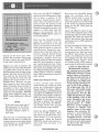
Service Note Order Form
Instructions
If you want service notes, please
check the appropriate boxes below
and return this form separately to
one of the following addresses.
For European customers (ONLY)
Hewlett-Packard
Central Mailing Dept.
P. 0. Box 529
Van Hueven Goedhartlaan 121
AMSTELVEEN-1134
Netherlands
All Others
Hewlett-Packard
1820 Embarcadero Road
Palo Alto, California 94303
NAME
COMPANY NAME
ADDRESS
CITY
STATE
0 180AlAR-12
0 180ClD-4
q
:
0 400ElEL-11
0
0
0
0
0
1114A-1
1302A-2
1304A-2
13118-14
1332A-9A
ZIP
0 3330AlB-14
0 3336AlBlC-1
0 3455A-17
0 3467A-2
0 3551A-7A
3551A-11A
3570A-8
3570A-9
3571A-2
0 3571A-3
0
0
0
0
0 3747AlB-13
0 3747AlB-14
0 3747AlB-15
0 3747AlB-16
0 3763A-3
3771AlB-SA
3771AlB-10
3771AlB-11
3771AlB-12
0 3771AlB-13
0
0
0
0
0 5427A-02
0 55OOC-215501
A
5
0 5501A-6
0 4943A-2
0 5505A-6
0 4943A-3
0 5505A-7
0 6140A-1
0 7010B-11
0 4943A-4
0 4943A-7
0 4944A-1A
70158-1 (SAFETY)
0 713017131-4
0 7310A-1
0 4944A-6
0 5036A-1
0 816OA-3
0 3771AlB-16
0 3777A-1
0 5045A-20
0 1610B-1
0 1640A-4A
0 1640A-8
0 1715A-5
0 17228-2
0 1725A-4
0 3585A-2
0 3711A-1
0 3712A-1
0 37t2A-2
0 3712A-3
0 1741A-9
0 2804A-3
0 3045A-1
0 3730A-5
0 3737A-2
0 3738A-3
0 3779B-15
0 3311A-2
0 3739A-3
0 3744A-1
0 37790-16
0 37798-17
0 3790A-9
0 3745AlB-228
0 1600A-3
0 1610A-10
0 4328A-7
0 5420A-23
0 5420A-24
0 4944A-2
0 4944A-3
0 3571A-4
0 3582A-3
0 3582A-4A
0 3582A-5
0 3582A-6
0 1336A-1A
0 1350A-6
0 4140A-1
0 4140A-2
0 4262A-9
0 4282A-6
0 3771AlB-14
0 3771AlB-15
0 8165A-2A
0 8165A-3A
0 3777A-2
0 3312A-3
0
0
0
0
0
0
3325A-3
3325A-5
3325A-6
3330AlB-11
3330AlB-12
3330AlB-13
0
0
0
0
0
3745AlB-33
3745AlB-34
37454918-35
3745AlB-36
3747AlB-4A
0
0
0
0
5315AlB-1
53268153278-10
5328A-258
5328A-26
0 5340A-9A
0 8170A-3
0 5340A-13A
0 5345A-10A
0 5359A-1
0 5359A-2
0 5363A-5
0 8568A-22
0 3791A-6
0 53638-1A
0 8620C-4
0 3791B-1
0 53638-4
0 53636-5
0 8662A-2
0 11713A-1
0 5370A-6
0 59309A-5
0 5420A-21A
0 59403A-5
0 69423A-1
0
0
0
0
0
0
0
0
0
0
3779A-14
3779A-15
3779A-16
3779A-17
37798-14
3792A-5
3793A-1
37938-1
3964A-1713968A-17
3964A-1813968A-18
WWW.HPARCHIVE.COM
0 5420A-22
0 8170A-4
0 8411A-4
0 8566A-1A
0 8568A-8A
0 8568A-23
0 8568A-24
0 8568A-26
0 8568A-27
..-.
.
COURSE
0
I
\
141
8552
8553
8554
DATE
-
..
. $"
COORDINATOR1
LOCATION
COST
Aug. 6-8
$3OOlStudent
-
OCCC
OJJJ
-
8568A
u {
Sept. 15-19
Sept. 22-26
Sept. 29-Oct. 3
$400/Student
0
3060
-
Aug. 18-29
Oct. 20-31
$2,10O/Student
0
DTS-70 -
Nov. 17-21
$1,00O/Student
Aug. 25-29
$400/Student
I
Jim Boyer
1400
Parkway
- - - Fniint,ain
- .
. Grnve
-. .- . - _
.
.
.
Santa Rosa, CA 95404
(707) 525-1400
J
Sandy Selleck
P.O. Box 301
Loveland, CO 80537
(303) 667-5000
Steve Thomas
1501 Page Mill Road
Palo Alto, CA 94304
Registration Instructions
To enroll in any of the seminars, contact
your local HP office and specify the course
desired. Please note that the 8566Al8568A
Spectrum Analyzer seminar is being repeated three consecutive weeks. Contact the
factory coordinator to specify which week
you desire.
c-
Upon receipt of your registration, we will
confirm your enrollment by returning all
necessary prestudy material along with a
list of nearby motel accommodations and reservation forms. Attendees are responsible
for their own transportation, accommodations, and meals.
Bulk Rate
US. Postage
1820 Ernbarcadero Road
Palo Alto, California 94303
Sunnyvale, CA.
BENCH BRIEFS
Permit No.
MAY-JUNE 1980
Volume 20 Number 3
Service information from
Hewlett-Packard Company
To obtain a qualification form for a free
subscription, send your request to the
above address.
Reader comments or technical article
contributions are welcomed. Please
send them to the above address,
attention Bench Briefs.
Editor: Jim Bechtold, HP Mt. View
California
Address Correction Requested
All rights are resewed
No part of bench Briefs may be reproduced without the express consent of the Edltor. The
Printed in U.S.A.
Editor may be telephoned at (415) 968-9200. Extension 376
... .
.... .
.-