1
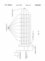
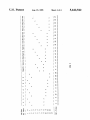
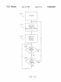
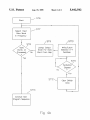
US005442542A
United States Patent 1191
[11]
[45]
Cook
[54] MACHINE STATE VIRTUALIZER
[76] Inventor:
Steven R. Cook, 2575 S. Bayshore
Dr., Suite 8A, Coconut Grove, Fla.
33133
[21] Appl. No.: 700,705
[22] Filed:
May 16, 1991
[51]
Int. Cl.6 ............................................ .. GOSB 19/02
[52]
US. Cl. ............................. .. 364/140; 364/709.01;
[58]
Field of Search .............................. .. 364/140-147,
364/709.11
364/191, 709.14, 709.15, 709.11, 709.09, 709.12,
'
[56]
709.13, 709.16, 709.01; 370/60
References Cited
U.S. PATENT DOCUMENTS
Patent Number:
Date of Patent:
5,442,542
Aug. 15, 1995
National Semiconductor, CMOS Logic Databook, pp.
5-56, 1988.
Omega Engineering, Inc., “AT-DIO-32F” The Data
Acquisition and Control Handbook Catalogue, pp.
D-62-D-64, 1990.
Micromint, BCC180 brochure, “Catalog of Embedded
Controllers”, pp. 16-17, 1991.
“Crosspoint Switches Seek Bandwidth”, EDN, Mar.
21, 1991, p. 3.
Morgan, Don, “Understanding the GPIB”, Dr. Dobb’s
Journal, pp. 48, 50, 52-53, and 92, Apr., 1991.
Liebson, Steve, The Handbook of Microcomputer Inter
facing, 2nd Edition, pp. 144-179.
Tandy Corporation, Realistic Service ManuaL
PRO-2006 Programmable Scanner, Catalogue No.:
20-145/9145, pp. 5, l7, and 77-78, 1990.
Primary Examiner--Roy N. Envall, Jr.
Assistant Examiner-Thomas E. Brown
2/ 1986
Chan ................................. .. 364/143
Attorney, Agent, or Firm-Evenson, McKeown,
4,672,602
6/1987
Hargrave et a1. . . . .
Edwards & Lenahan
4,679,135
7/1987
Kobayashi et a1. .... ..
364/146
4,757,463
7/ 1988
Ballou et a1. .
395/905
4,570,216
. . . .. 370/58
5,144,548 9/1992 Salandro
364/191
[57]
ABSTRACI‘
OTHER PUBLICATIONS
A machine state virtualizer is an apparatus for control
ling an electronic device having a switch matrix of
X-lines and Y-lines (sometimes referred to as crosspoint
switches) with a microcomputer. The device includes a
Datametrics, Inc., “Communications Manager” bro
lines and Y-lines of the electrical device. A microcom
chure, 1989.
Electronic Equipment Bank, 1 990 EEB Shortwave Cata
log, pp. 10-11, 1990.
Keithley, MCPT-SX8 Metrabus Crosspoint Matrix Relay
Boards, “Data Acquisition Land Control” Catalogue,
vol. 24, p. 238, 1991.
Harris
Semiconductor/RCA
Solid
State,
puter references a machine state virtualization map and
outputs data corresponding to a desired machine state.
The output data is then decoded and used to control the
plurality of switches so as to virtualize the desired ma
chine state of the electronic device. The microcomputer
utilizes sequences and rules for implementing a de?ned
5,179,552
l/l993
Chao
5,249,115
9/1993
Reid .................................. .. 364/141
... ..
. . . ..
370/60
plurality of switches which interconnect speci?ed X
device control objective.
“CD54/74HC22106, CD54/74HT22106” brochure,
3 Claims, 6 Drawing Sheets
Jul. 1985.
X-SWITCH ARRAY 4
X-SWITCH
DEVICE SELECTOR 2
>
X~SWITCH POLES 6
Y_SWITCH ARRAY 5
Y-SWITCH POLES 7
MICRO
COMPUTER 1
Y-SWITCH
DEVICE
SELECTOR 3
/
N
e-—-—
TPl
FEEDBACK DEVICE 8
US. Patent
Aug. 15, 1995
Sheet 3 0f 6
5,442,542
Yum
mU;
US. Patent
Aug. 15, 1995
S‘i'i
\
Sheet 5 of 6
Initialize
5T2
\
Set Next
Frequency
\ (see Device Driver)
3T3
Wait F or
\
Minimum
Duration
ST4
\
Signal
Detected
Yet
Duration
Elapsed
?
No
Fig 4a
5,442,542
US. Patent
Aug. 15, 1995
Sheet 6 of 6
5,442,542
/ ST6
Start
Select Next
Data Word
/
ST7
In Frequency
ST8
Data
/
/ ST9
/STlO
.
Lookup Output
Words All
State For Data
Processed
Word From Mop
Write/Latch
7
Selected X-Y
Switches
Yes
Set tlo time
Elapsed
’)
SW2 \
Clear Switch
Data
/ sm
l___,___
Continue Main
Program Sequence
Fig 4b
1
5,442,542
MACHINE STATE VIRTUALIZER
2
puter. Accordingly, the device of this invention has
widespread applications and can be used to control any
electrical device which uses switches or responds to
BACKGROUND OF THE INVENTION
devices typically are provided with switches to enable a
user to manually initiate and control their various appli
cations.
logic states. However, one speci?c advantageous use of
the device of this invention is the use thereof to control
radio devices.
A typical electronic device incorporates an elec
tronic keypad having an X-Y network of switches
(sometimes referred to as a crosspoint switch network).
The X-Y lines are interconnected by keystrokes, and
data is generated thereby and forwarded to other blocks
Generalized process control according to the prior
art usually involves limited switching of electrical de
of the device through simple logic state switching, pulse
coded switching and other strategies. Depending upon
vices (e.g., a heater is turned on via a relay if tempera
ture falls to a certain level). Such control strategies
typically employ a device controller such as the 8255
the device, the X-Y switch network may be used to
input data to a microcontroller. The signals switched by
Device and process control in prior art electronics
applications is generally achieved through special pur
pose circuitry using either simple gate logic or more
complex microprocessor controllers. Such prior art
the keypad may include non-standard states and/or
programmable peripheral controller and the necessary
timed pulses, thus rendering simple logical control unre
hardware and software drivers. Thus, a logic state con
trols a semiconductor or mechanical relay which in turn
switches a control voltage. Such a design is acceptable
if the device to be controlled is engineered to respond to
liable. The device of this invention overcomes the unre
simple logic signals, or has simple control needs which
liability by connecting directly to the X-Y circuits and,
under microcomputer control, by virtualizing the key
strokes for which an electronic device was designed.
BRIEF DESCRIPTIONS OF THE DRAWINGS
can be accommodated through patterns of parallel data.
However, such a control design is not acceptable for
FIG. 1a is a block diagram of a ?rst preferred em
situations wherein control of large numbers of states is 25 bodiment of the invention;
necessary, for control of analog applications, or for
FIG. lb is a block diagram of a second preferred
control of more complex switch strategies such as non
embodiment of the invention;
standard states and time-sensitive requirements.
FIG. 2 is a schematic diagram of a speci?c implemen
In certain specialized ?elds there are standards and
tation
of the device of the invention according to the
conventions governing the interaction among various 30
?rst
preferred
embodiment;
devices engineered to conform to these standards. For
FIG. 3 shows an exemplary keypad logic analysis
example, IEEE 488 is a recognized standard for inter
map;
.
device communication. Other examples of such stan
FIG.
4a
is
an
exemplary
?owchart of the main pro
dards are MIDI, which is used for control of musical
gram
sequence;
and
instruments, and the proprietary CI-V standard pub 35
FIG. 4b is an exemplary ?owchart of the device
lished by ICOM America for the control of radio de
driver
sequence.
vices. Most devices which are part of such a con?gura
tion are generally also controllable through switches
DETAILED DESCRIPTION
and similar means. Unfortunately, these existing stan
According
to the ?rst preferred embodiment of the
dards and the associated control schemes require spe 40
invention,
four
X-switch poles 6 and eight Y-switch
cialized engineering of the electrical device and adher
poles 7 are hard-wired to the X-Y circuits of an elec
ence to rigorous pre-set standards.
tronic device to be controlled. As shown in FIG. 1a, an
Basic multiplexer techniques have been developed
X-switch array 4 is provided to electronically switch
for applications such as the computer data/control bus,
audio/video switching, and telephonic switching, how
45 each of the X-switch poles to a common line TP1. Simi—
ever, such devices and the necessary software and pro
cesses have not been developed for general device and
process control.
Because of the lack of a universal standard for device
larly, a Y-switch array 5 is provided to electronically
switch each of the Y-switch poles to the common line
control, and because of the multiplicity of machine
functions, intended users and disparate design strate
gies, a unifying approach for the control of electronic
devices is unknown in the prior art.
crocomputer 1 through X-switch device selector 2 and
Y-switch device selector 3, respectively. The mi
TPl. Electronic control of the X-switch array 4 and
Y-switch array 5 is effected under the control of a mi
crocomputer 1 provides control signals representative
of machine states of the device to be controlled, and
forwards these control signals to the device selectors.
SUMMARY OF THE INVENTION
55 The device selectors then decode these control signals
and control the individual switching of the switch ar
The device of this invention overcomes the disadvan
rays thereby. A feedback device 8 is provided which
tages of the prior art discussed above and allows a uni
provides a feedback signal from the electronic device to
versal approach to device control by interaction with
the microcomputer 1.
the device’s own switches and existing control facilities,
A second preferred embodiment of the invention is
and by use of the device’s own signal levels and timings.
shown in FIG. 1b, wherein corresponding elements
The control infrastructure of the device of this inven
from FIG. 1a are denoted by the same reference numer
tion initiates and manages the controlled device, not
als. In the second preferred embodiment, the device
through imposing external control events as in the prior
selectors are replaced by a switch selector/latch 9
art, but by virtualizing the very events for which the
65 which controls a 32-unit electronic X-Y switch array
machine was designed.
10. The X-Y switch array 10 implements a switch ma
The device of this invention is a generalized interface
trix of the eight Y-switch poles 7 and the four X-switch
which implements state switching, electronic device
poles 6. Thus, electrical interconnection between any
control, and related applications using a microcom
3
5,442,542
Y-switch pole and any X-switch pole may be achieved
under control of the switch selector/latch 9. Feedback
device 8 is also provided in the second preferred em
bodiment.
A more detailed schematic diagram of the ?rst pre
ferred embodiment of the invention is shown in FIG. 2,
wherein the device is used to control a 4X 8 X-Y switch
network.
Exemplary component values are included in the
discussion of this preferred embodiment. However,
4
The outputs Y0-Y3 of U1 are fed to switch poles
E0-E3 of four bilateral switches incorporated in switch
device U5. Similarly, the eight outputs Y0-Y7 of data
distributor U2 are fed to terminals E0-E3 on each of ‘
two such switch devices U3, U4. Switch devices U3-U5
are preferably 4066 CMOS bilateral switches. Output
lines Y0-Y3 and Y0—Y7, together with unused pins
Y4-Y15 on U1, are held in a “default-low” state by
resistor packs RP2-RP4 (preferably 100 kOhm). In
other embodiments, such as higher energy applications,
the apparatus of the invention could utilize alternative
determination of these values in this or a similar circuit
switch devices including solid state relays, other semi
would be apparent to one skilled in the art.
conductor switches, and mechanical relays.
CNl is a connector which is attached, for instance, to
Terminals Y0—Y3 of switch device U3, and terminals
a parallel port of an IBM PC compatible microcom
puter. CN1 includes ten lines, seven of which are data 15 YO-Y3 of switch device U4, are connected via CN2 to
the Y-signal lines of the device to be controlled. Simi
lines, one of which is an input/output control, one of
larly, terminals Y0-Y3 of switch device US are con
which is ground, and the last of which (RAD) reads a
nected via CN2 to the X-signal lines of the device to be
signal from another connector CNS, discussed below. A
controlled. Terminals 20-23 of each of switch devices
resistor pack RPl, preferably having a resistance of 2.2
kOhm, is provided to pull up the voltage on the data 20 U3-U5 are connected to a common bus TP1. In addi
and I/O lines.
A second connector CN2 is provided through which
the device is connected to the X-Y switch matrix of the
tion to its bus function between the switch devices, TP1
can be used to send or receive a signal via the TPl line
in CN3 to or from one or more of the X-Y lines.
device being controlled. In this embodiment, CN2 in
cludes eight Y-signal lines, four X-signal lines, and a
ground line.
The 12 unused lines of data selector U1 may be used
to virtualize a larger X-Y network. However, these
lines may also be used for security purposes to serialize
from the receiver on this line.
the data lines such that a desired machine state is virtu
4,096 possible combinations concealed under the IC for
The third connector CN3 provides power and access
veri?cation of proper connection and password protec
to other external signals. According to this embodi‘
tion. In this case, a diode should be inserted on the Z
ment, CN3 is provided with ?ve lines: a TPl line; a 30
line of data distributor U1 to permit data to be written
receiver activity detection (RAD) line; voltage in (Vin);
to both data selectors while restricting input to U1 and
voltage regulated (Vreg); and ground (GND). The TPl
another 4049 buffer could be used to read the password
line allows external access to or from the switch matrix,
information from U1.
as will be discussed in more detail below. The receiver
The microcomputer 1 embodies a table which maps
activity detection line allows the microcomputer to 35 machine states of the controlled device to data values
monitor receiver activity via a buffer U6 (preferably a
and controls switch timing and sequence. Mapping of
4049 hex inverting buffer) which captures a signal input
the machine states allows the microcomputer to control
Vin provides power to voltage regulator VRl. Volt
alized. According to the preferred embodiments, the
age regulator VRl comprises a 78LO5 voltage regula 40 microcomputer is programmed to execute control rou
tor U7 and a ?lter capacitor C3. The ?lter capacitor
preferably has a value of 500 mf. The output of VRl is
connected to the Vreg line, and is used to power the rest
of the circuit. A power supply ?lter capacitor C1 (pref
erably 10 mt) is connected in parallel between Vreg and
ground to properly condition voltage. Voltage regula
tion could, of course, be provided externally, in which
case Vin would be superfluous and a regulated voltage
tines which require virtualization of a sequence of ma
chine states, thus automating operation of the con
trolled device. For example, the microcomputer can be
programmed to execute a radio scanning management
45 routine such that a user may step through scanned chan
nels automatically without using keystrokes normally
necessary to operate the device directly. The mi
crocomputer may also be programmed so that the chan
could simply be applied to Vreg. Capacitor C2 (prefera
nel is changed only when the receiver activity detection
bly 0.1 mt) is connected between Vreg and ground to 50 line indicates that the receiver is inactive. Clearly, an
?lter signal noise.
unlimited number of control routines applicable to all
Four of the data lines from CNl are fed to a data
electronic devices with switches are available using the
device of the invention.
cuit. The four data lines are connected to terminals
The steps necessary to develop a machine state-data
AO-A3 of the data selector U1, and are used to control 55 map will now be discussed with speci?c reference to the
the output of terminals Y0-Y3. Because only four X-sig
Radio Shack PRO2006 scanning radio, a consumer
nal lines are being controlled in this embodiment, only
radio device not designed to facilitate external mi
four of the Y terminals of U1 are being utilized. How
crocomputer control. First, the number of X and Y lines
ever, the four data lines are sufficient to control up to 16
utilized by the device’s front panel keypad are deter
outputs (Y0-Y15) of U1, if necessary.
60 mined from examination of the device and/or documen
Similarly, the remaining three data lines from CNl
tation. Second, an interconnection strategy is developed
are fed to terminals A0—A2 of data selector U2, which
to assign X-Y lines of the radio to the switch arrays of
is preferably of the 4061 type. The three data inputs are
the Machine State Virtualizer. As in the preferred em
used to control output of terminals Y0-Y7 of U2. An
bodiments discussed above, all X lines are preferably
inhibit line TP2, connected to the inhibit pins of U1 and 65 connected to switches controlled by one data selector,
U2, is provided so that the data selectors may be inhib
while all Y lines are preferably connected to switches
ited if so desired via a manual switch or an electronic
controlled by another data selector. Third, a data value
data selector.
is assigned to each data line according to the necessary
selector U1, which is preferably a 4067 integrated cir
5
5,442,542
6
circuitry. In the speci?c implementation of the ?rst
preferred embodiment discussed above, three data lines
relating to the connection of the external hardware of
the device of the invention to the microcomputer.
are used to control eight switches corresponding to the
The reset instruction is a command required by the
Y-signal lines, and four data lines are used to control
Machine State Virtualizer circuitry to prepare it for the
four switches corresponding to the X-signal lines (leav 5 next state. It would typically instruct the device to turn
ing 12 outputs unused). The feedback device is con
all switches off and would be issued at ST6 and ST12
nected to an available receiver circuit which indicates
during the procedures described below.
radio signal detect status and in turn makes such data
available to the Machine State Virtualizer. Lastly, a
map is developed which correlates X-Y switch intersec
The latch instruction is the means of controlling in
traswitching states to maintain switch contact closure
while both X and Y switches are being selected and
activated and for a de?ned time interval. Latching may
tions to data values.
The map is adjusted for any remaining data lines
which may be needed for device selection or other
functions. From this map, the microcomputer adds the
data bits together to determine the byte necessary to
virtualize a desired keystroke. In this way, the logic
states of the computer are used to effect interconnection
be controlled via software (e.g., constantly resending
switching commands) or hardware (e.g., circuitry in
cludes lines for latch initiation and termination). The
circuit of the ?rst preferred embodiment, shown in
FIG. 2, utilizes the hardware latches contained within
the microcomputer 1.
Timing parameters are intervals required by the de
vice being controlled in order to properly receive key
strokes. Such timing parameters must be determined for
of switching circuits in the device rather than to apply
the logic states of the computer directly to the device as
in the prior art. FIG. 3 shows a keypad logic analysis
map for the RS PRO2006 radio. An “X” is placed in the
each device and include minimum state time for host
map corresponding to X-Y intersections of the relevant
decoding and minimum interkey time. Such times may
key. For this scanner, CN601 pins 1-8 are high when
vary based on individual switches, sequence of strokes,
open and effect one low, variable duration pulse when
the mode a machine is operating in and similar factors.
closed. CN601 pins 9-12 are low open and high closed. 25
Once initialization is complete, the frequency is then
A full discussion of the features and keypad logic of the
set in ST2. FIG. 4b is a flowchart of the device driver
PRO2006 scanner can be found in the PRO2006 service
sequence whereby the function of setting the ?rst or
manual.
subsequent frequency (5T2) is performed for a particu
One advantageous use of the Machine State Virtual
lar device.
izer is to control frequency scanning of a radio device 30
Referring to FIG. 4b, the device driver sequence is
such as the PRO2006 scanner. A ?owchart illustrating
entered at “start” step ST6. The sequence then proceeds
the main program sequence to perform this function is
to select the ?rst or subsequent data word in the fre
shown in FIG. 4a. STl is an initialization step during
quency (ST7), and determines if all data words have
which rules and/or parameters are established from
been processed (8T8). If the answer in ST8 is yes, the
stored machine instructions, override rules and/or pa 35 driver returns to the main program sequence (ST13). If
rameters are established from data ?les and from user
the answer is no, the output state for the selected data
input, and the Machine State Virtualizer hardware is
initialized. The initialized parameters include communi
cation parameters (frequency settletime, minimum dura
word is looked up from the map (8T9), and the output
input port address, reset instruction, latch instruction,
and timing parameters).
4a), the sequence waits for the minimum duration (8T3)
may be set at zero for sampling, or at 99 for an unlimited
above, the device of the invention provides for a plural
state is written and latched to the X-Y switches (ST10).
The driver waits for a predetermined keystroke sett
tion, maximum duration, delay, priority frequencies, 40 letime to elapse (STll), and then clears the switch data
and logging mode) and device driver parameters (data
(ST12) and returns to ST7 to select the next data word.
output port address, control output port address, data
Returning now to the main program sequence (FIG.
and then determines whether a signal has been detected
The frequency settletime parameter causes the con 45 (ST4). The minimum duration was set to a predeter
trolled radio device to pause for a brief period (typically
mined duration during the initialization step. If a signal
around 0.050 seconds) after tuning to a frequency but
has not been detected, the sequence returns to ST2. If a
before commencing other procedures. This brief pause
signal has been detected, it is then determined whether
is helpful in situations wherein the tuning circuits re
the maximum duration has elapsed. The maximum dura
quire time to converge to a frequency or when other
tion was also set to a predetermined duration during the
delays occur. The minimum duration parameter slows
initialization step. If the maximum duration has elapsed,
down the scan speed so that frequencies are monitored
the sequence returns to ST2. If it has not, the sequence
for the minimum duration even if no signal is present.
loops through states ST4 and STS until a signal is no
The default value for this parameter is zero. The maxi
longer detected or the maximum duration elapses.
mum duration parameter limits the maximum time a 55
When the device of the invention is used to control
particular frequency will be monitored. This parameter
frequency scanning of a radio device as described
duration. The delay parameter causes scanning to pause
on a frequency after completion of a reception to deter
mine if a new signal is detected during the delay period.
This is useful for monitoring two-way communications
which may have periodic interruptions. The default
value for this parameter is 2.0 seconds. Priority frequen
cies are user-designated priority channels. Lastly, log
ity of user interrupt events to facilitate use thereof. User
interrupts may include displaying help information,
displaying the present date, modifying parameters, set
ting frequency exclusion rules, pausing, resuming to the
next frequency, altering the display, setting frequency
selection rules, editing frequency records, and ending
the control sequence. In addition, the device of the
ging mode refers to whether a computer record is kept 65 invention provides a plurality of utility routines, includ
of scanning activity.
The data output port address, control output port
address, and data input port address are parameters
ing for example routines for building and editing fre
quency ?les, performing de?ned receiver operations,
logging data regarding signal activity, editing parame~
7
5,442,542
8
2. A universal controller for controlling an external
electronic device having a switch matrix of X-lines and
ters and rules, displaying information, and preparing
reports.
Y-lines, comprising:
It is apparent that the invention could be used to
control multiple devices, or to control a larger number
of switches by cascading more than one Machine State
Virtualizer unit or by expanding its circuitry.
The system can also be implemented with large scale
(A) a ?rst plurality of switches each having a ?rst
terminal adapted to be connected to the X-lines of
said external electronic device and a second termi
nal connected to a common line;
integration multiplexers such as the con?guration re
?ected in FIG. 1b. This latter implementation actually 10
utilizes electronic switches at each of the unique X, Y
(B) a second plurality of switches each having a ?rst
terminal adapted to be connected to the Y-lines of
said external electronic device and a second termi
nal connected to said common line;
intersections rather than the X-selection to Y-selection
(C) control means for controlling said ?rst plurality
described in the ?rst preferred embodiment, however
of switches and said second plurality of switches so
the functionality as it relates to the objective of the
device is identical.
As previously indicated, the Machine State Virtual
as to virtualize a desired machine state of the exter
nal electronic device,
(1) wherein said control means comprises a ?rst
data selector which controls said ?rst plurality of
izer can be utilized to control any electronic device
switches and a second data selector which con
which contains switches. The description of radio scan
trols said second plurality of switches, and stor
ning is presented as only one example of the applica
age means for storing a machine state virtualiza
tions of the device of the invention.
While there are shown and described present embodi
ments of the invention, it is to be distinctly understood
that the invention is not limited thereto, but may be
otherwise variously embodied and practiced within the
scope of the following claims.
What is claimed is:
1. A universal controller for controlling an external
electronic device having a switch matrix of X-lines and
Y-lines, comprising:
tion map,
(2) wherein said machine state virtualization map
correlates X-line and Y-line intersections of said
electronic device to data values corresponding
25
to a machine state,
(3) wherein said control means further comprises
processing means for processing a control rou
tine instruction by referencing said machine state
virtualization map and outputting data values
30
(A) switch means adapted to be connected to the
X-lines and the Y-lines and comprising a plurality
corresponding to a sequence of desired machine
states to said ?rst data selector and said second
data selector; and
(D) feedback means for obtaining feedback from the
electronic device, wherein said processing means is
of switches for selectively interconnecting X-lines
and Y-lines of the external electronic device;
35
(B) control means for controlling said'switch means
responsive to said feedback means, and wherein a
sequence of events is altered based on preestab
lished rules when a predetermined signal is re
ceived from the feedback means.
3. A method of controlling an electronic device hav
so as to virtualize a desired machine state of the
external electronic device,
(1) wherein said control means comprises a data
selector which controls said plurality of switches 40 ing a switch matrix of X-lines and Y-lines, comprising
the steps of:
and storage means for storing a machine state
(A) inputting information indicative of a desired ma
virtualization map,
chine state of the electronic device;
(2) wherein said machine state virtualization map
(B) referencing a machine state virtualization map
correlates X-line and Y-line intersections of said 45
which correlates X-line and Y-line intersections of
electronic device to data values corresponding
the electronic device to data values corresponding
to a machine state,
to machine states to determine data values corre
(3) wherein said control means further comprises
sponding to said desired machine state;
processing means for processing a control rou
tine instruction by referencing said machine state 50
virtualization map and outputting data values
corresponding to a sequence of desired machine
states to said data selector; and
(C) decoding said data values;
(D) virtualizing keystrokes determinative of the de
sired machine state by interconnecting the X-lines
and Y-lines under control of the decoded data val
ues;
(C) feedback means for obtaining feedback from the 55
electronic device, wherein said processing means is
responsive to said feedback means, and wherein a
sequence of events is altered based on preestab
lished rules when a predetermined signal is re
ceived from the feedback means.
60
65
(E) receiving feedback from the electronic device;
and
(F) altering a sequence of events when a predeter
mined sequence of events occurs, wherein said
predetermined sequence of events is de?ned by a
set of program rules.
*
*
*
*
*