1
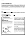
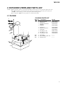
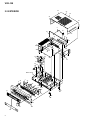
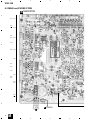
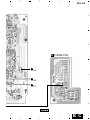
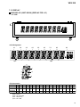
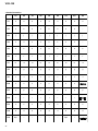
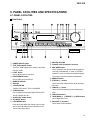
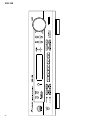
ORDER NO.
RRV2146
AUDIO MULTI - CHANNEL RECEIVER
VSX-108
THIS MANUAL IS APPLICABLE TO THE FOLLOWING MODEL(S) AND TYPE(S).
Type
Model
VSX-108
KUXCN
Power Requirement
Remarks
AC120V
CONTENTS
1. SAFETY INFORMATION ...................................... 2
2. EXPLODED VIEWS AND PARTS LIST ............... 3
3. BLOCK DIAGRAM AND SCHEMATIC DIAGRAM ..... 6
4. PCB CONNECTION DIAGRAM ......................... 17
5. PCB PARTS LIST ............................................... 22
6. ADJUSTMENT .................................................... 24
7. GENERAL INFORMATION ................................
7.1 PARTS ..........................................................
7.1.1 IC ............................................................
7.1.2 DISPLAY .................................................
8. PANEL FACILITIES AND SPECIFICATIONS .......
26
26
26
33
35
PIONEER CORPORATION
4-1, Meguro 1-chome, Meguro-ku, Tokyo 153-8654, Japan
PIONEER ELECTRONICS SERVICE, INC. P.O. Box 1760, Long Beach, CA 90801-1760, U.S.A.
PIONEER ELECTRONIC (EUROPE) N.V. Haven 1087, Keetberglaan 1, 9120 Melsele, Belgium
PIONEER ELECTRONICS ASIACENTRE PTE. LTD. 253 Alexandra Road, #04-01, Singapore 159936
c PIONEER CORPORATION 1999
T – IZE OCT. 1999 Printed in Japan
VSX-108
1. SAFETY INFORMATION
This service manual is intended for qualified service technicians ; it is not meant for the casual do-ityourselfer. Qualified technicians have the necessary test equipment and tools, and have been trained
to properly and safely repair complex products such as those covered by this manual.
Improperly performed repairs can adversely affect the safety and reliability of the product and may
void the warranty. If you are not qualified to perform the repair of this product properly and safely, you
should not risk trying to do so and refer the repair to a qualified service technician.
WARNING
This product contains lead in solder and certain electrical parts contain chemicals which are known to the state of California to cause
cancer, birth defects or other reproductive harm.
Health & Safety Code Section 25249.6 – Proposition 65
NOTICE
(FOR CANADIAN MODEL ONLY)
Fuse symbols
(fast operating fuse) and/or
be of identical designation.
(slow operating fuse) on PCB indicate that replacement parts must
REMARQUE
(POUR MODÈLE CANADIEN SEULEMENT)
Les symboles de fusible
(fusible de type rapide) et/ou
de remplacement doivent avoir la même désignation.
(fusible de type lent) sur CCI indiquent que les pièces
(FOR USA MODEL ONLY)
1. SAFETY PRECAUTIONS
The following check should be performed for the
continued protection of the customer and service
technician.
ANY MEASUREMENTS NOT WITHIN THE LIMITS
OUTLINED ABOVE ARE INDICATIVE OF A POTENTIAL
SHOCK HAZARD AND MUST BE CORRECTED BEFORE
RETURNING THE APPLIANCE TO THE CUSTOMER.
LEAKAGE CURRENT CHECK
Measure leakage current to a known earth ground (water
pipe, conduit, etc.) by connecting a leakage current tester
such as Simpson Model 229-2 or equivalent between the
earth ground and all exposed metal parts of the appliance
(input/output terminals, screwheads, metal overlays, control
shaft, etc.). Plug the AC line cord of the appliance directly
into a 120V AC 60Hz outlet and turn the AC power switch
on. Any current measured must not exceed 0.5mA.
Reading should
Leakage not be above
current 0.5mA
tester
Device
under
test
Test all
exposed metal
surfaces
Also test with
plug reversed
(Using AC adapter
plug as required)
AC Leakage Test
2
Earth
ground
2. PRODUCT SAFETY NOTICE
Many electrical and mechanical parts in the appliance
have special safety related characteristics. These are
often not evident from visual inspection nor the protection
afforded by them necessarily can be obtained by using
replacement components rated for voltage, wattage, etc.
Replacement parts which have these special safety
characteristics are identified in this Service Manual.
Electrical components having such features are identified
by marking with a on the schematics and on the parts list
in this Service Manual.
The use of a substitute replacement component which does
not have the same safety characteristics as the PIONEER
recommended replacement one, shown in the parts list in
this Service Manual, may create shock, fire, or other hazards.
Product Safety is continuously under review and new
instructions are issued from time to time. For the latest
information, always consult the current PIONEER Service
Manual. A subscription to, or additional copies of, PIONEER
Service Manual may be obtained at a nominal charge from
PIONEER.
VSX-108
2. EXPLODED VIEWS AND PARTS LIST
NOTES:
• Parts marked by "NSP" are generally unavailable because they are not in our Master Spare Parts List.
• The mark found on some component parts indicates the importance of the safety factor of the part.
Therefore, when replacing, be sure to use parts of identical designation.
• Screws adjacent to mark on the product are used for disassembly.
2.1 PACKING
• PACKING PARTS LIST
11
Mark No.
1
2
3
2
9
1
3
5
13
8
6
Description
Part No.
01582100001S
06410001003S
152010801297
4
AM Loop Antenna
FM Antenna
Operating Instructions
(English)
Polyform L
5
6
7
Polyform R
Remote Control Unit
Carton Box
14901082000S
18201080001S
153010820297
8
9
10
Poly. Bag (4 × 20)
Poly. Bag (10 × 15)
Poly. Bag (20 × 26)
15004011210S
15010015510S
15020026510S
11
12
13
RCA Cable
Dry Cell Battery (LR6, AA)
Warranty Card
•••••
•••••
•••••
14901081000S
10
4
12
NSP
NSP
NSP
7
3
VSX-108
23
2.2 EXTERIOR
25
25
25
25
9
30
24
25
26
34
25
26
26
25
26
25
25
25
28
25
33
32
A
28
1
25
28
25
25
27
5
31
4
2
21
29
25
20
3
Bottom Cover
25
25
17
25
19
7
6
25
25
25
A
19
19
25
25
14
18
25
25
25
22
12
25
25
22
15
25
13
11
10
4
25
25
VSX-108
• EXTERIOR PARTS LIST
Mark No.
Description
Part No.
TUNER PCB
(Circuit Parts Assy)
MAIN PCB
(Circuit Parts Assy)
PHONE PCB
(Circuit Parts Assy)
AZW7259
AC O/P PCB
(Circuit Parts Assy)
AC I/P PCB
(Circuit Parts Assy)
PW SW PCB
(Circuit Parts Assy)
AZW7259
AZW7259
8
9
10
DISPLAY PCB
(Circuit Parts Assy)
•••••
AC Cord Stopper
Display Lens
13000000001S
11701080101S
11
12
13
14
15
Volume Knob
Front Panel
Front Cabinet
Power Button
Function Button
12701081010S
10801080010S
10101080001AS
12801080001S
12801082001S
16
17
18
19
20
•••••
Mounting Bracket A
Mounting Bracket B
PCB Holder
Mounting Holder
12901089000S
12901089100S
13001082000S
13301082310S
21
22
23
24
25
PCB Mounting Bracket
Insullator
Top Cover
Rear Cover
Screw
13301083310S
13821007010S
18001083010S
18001085101S
BBZ30P080FZK
26
27
28
29
30
Screw
BBZ30P100FZK
Screw
FBT40P080FZK
Screw
14453016202S
Power transformar (AC120V) 01801088522S
AC Power Cord
02360040009S
31
32
33
34
Fuse (F801 : 4A/250V)
Metal Washer
PCB Mounting Bracket
Heatsink Mounting Bracket
NSP
1
NSP
2
NSP
3
NSP
4
NSP
5
NSP
6
NSP
7
NSP
NSP
NSP
AZW7259
AZW7259
AZW7259
AZW7259
05005020402S
•••••
•••••
•••••
5
1
2
3
4
VSX-108
3. BLOCK DIAGRAM AND SCHEMATIC DIAGRAM
A
3.1 BLOCK DIAGRAM, OVERALL WIRING DIAGRAM, AC O/P, AC I/P
and PW SW PCBS
A
FM
ANTENNA
AM
ANTENNA
FM
CN102
TUNER PCB
1
FM
IC101
1
9
LA1186N
FM FRONT END
1
IC102
00201838-040 16
(LA1838)
17
ELECTRIC
TUNING
8
AM
2
TUNER
3
4
5
CN201
TUNER-R
1
GND
2
TUNER-L
+5V
+9V
IC203
00262419-010
(M62419)
Digital Sound Controller
26 17
L R
TONE
OUT
TUNER
3
36 L
4
7 R
5
34 L
27
9 R
30
TONE
Q102
35 L
8 R
CN708A
2
10 9
8
7
6
5
7
8
4
GND
9 10
3
2
33 L
CD
TV
CN701
VR
10 R
L
R
1
CN708
B
CN701A
AM/FM IF
6
EO
SD
5
AM SIG.
4
ST. IND
3
– AM
2
MONO
– FM
1
IF REQ.
GND
1
2
FM SIG
1
FADER
SELECTOR
1
SEL
OUT
L R
40 3
L R
39 4
L R
23 20
L
R
L
VCR
R
IN
75
FM IN
L
VCR
R
OUT
74
AM IN
61 62
CN6
CN702
1
DATA 9
2
3
DATA 50
4
IC701
00272358-040
(LC72358N)
Control µ-Com.
5
6
7
MUTE 53
8
9
10
C
RELAY 17
KEY SW
DATA
12
11
12
REMOTE
3
13
DATA
3
DATA
4
CLK
E2
7
8
OVER
9
10
11
12
13
CN707
CN7
1
6
2
IC702
00202879-040
(BU2879AK)
FL Driver IC
3
4
Q703,
Q704
5
6
+5V
1
2
V1
FL TUBE
04991693-001
7
AC3.8V
AC3.8V
-25V
+5V
GND
SR
GND
1
2
3
B MAIN PCB
B 1/2, B 2/2
4
5
6
7
CONTROL
OUT
IC703
06104421-000
IR Receiver
D
G DISPLAY PCB
6
1
2
3
C 31
S 33
6
MUTE
DC/O
CV,
SV
OUT
5
DGND
2-CH
IC201
00201041-040
(LV1041M)
51 Dolby Pro-Logic Decoder
2
E1
RELAY
IN
24 21
L R
OUT
1
CLK
SP.OFF
R
L
4
5
6
7
8
VSX-108
Note : When ordering service parts, be sure to refer to "EXPLODED VIEWS and PARTS LIST" or "PCB PARTS LIST".
A
• NOTE FOR FUSE REPLACEMENT
CAUTION - FOR CONTINUED PROTECTION AGAINST RISK OF FIRE.
REPLACE WITH SAME TYPE AND RATINGS ONLY.
: AUDIO SIGNAL ROUTE
C
IC204
STK407-070
2ch AF Power Amp.
CN14
RY2
3
L-SP
4
4
R-ST
5
SP-OFF
6
PHONES
2
GND
3
7
1
L
2
6
14
CN14A
R
1
RY1
10
PHONE PCB
5
6
B
SUB WOOFER
[Jack 5]
Q201-Q204
MUTING
L
FRONT
[Jack 6 (1/2)]
R
IC202
00206458-040
(LA6458S)
Dual Operational Amp.
CENTER
[Jack 6 (2/2)]
RY3
6
8
10
4
2
14
6
RY4
7
SURROUND
[Jack 7]
IC205
STK407-070
2ch AF Power Amp.
Q209-Q211
RELAY
DRIVER
C
CN207
2
D802
Q802
+5V
+9V
F
CN207A
1
AC
3.8V
3
REG.
4
Q803
5
1.9V
CT
1.9V
1
02041100-004
PS1
POWER
2
3
W1
4
16.5V
+B
LIVE
C823
R821
0.01/250V 120/1W
CN208
J6
1
2
–B
W2
05005020402S
F801
4A/250V W3
5
REG.
D803
PW SW PCB
3
AC120V
60Hz
W4
J5
NEUTRAL
J7
Q801
–25V
T1
POWER
TRANSFORMER
01801088522S
REG.
Q804
–9V
D
REG.
E AC I/P PCB
R820
3M3
D
AC POWER CORD
02360040009S
AC O/P PCB
5
6
7
D E F
8
7
1
2
3
4
VSX-108
3.2 TUNER PCB
A
A TUNER PCB
D101
00400321-500
(SVC321)
T101
01621032-104
TC101
01410200-003
AM
LOOP
ANTENNA
AM
Q101
00300715-041
(2SK715)
AM
AM
AM
AM
T102
01620360-023
Q103
00300608-045
(2SA608)
D102
00400321-500
(SVC321)
IC101
LA1186N
FM
Q105
00302999-044
(2SC2999)
FM
T103
01627539-032
FM
D106
SVC201SPA
D105
SVC201SPA
L102
01705037-350
L104
01706036-350
FM
FM
300Ω
CF101
02810700-009
CF102
02810700-009 FM
FM
FM
BPS101
02876108-002
B
FM
Q102
00302999-044
(2SC2999)
Q104
00300536-046
(2SC536)
C
Q106
00302999-044
(2SC2999)
Q107
00302999-044
(2SC2999)
IC101
D
8
A
1
(volt)
9
1
2
3
4
5
6
7
8
AM
0.0
0.0
0.0
0.0
0.0
0.0
0.0
0.0
0.0
FM
0.9
1.5
4.8
0.0
0.0
4.8
0.0
4.0
4.8
2
3
4
5
6
7
8
VSX-108
A
T
AM
FM
L101
01500393-001
: AM SIGNAL ROUTE
: FM SIGNAL ROUTE
T
T
AM
AM
: TUNER AUDIO SIGNAL ROUTE (L ch)
B
IC102
00201838-040
(LA1838)
CN102
T
02520005-205
FM
T104
01627580-041
B
CN201
GM74A
02810700-025
CF103
02800450-000
T
CN701A
02520012-202
C
G
CN701
G
CN708
CN708A
14
(volt)
15
0.0
8.0
12.0
0.0
12.0 12.0
IC102
1
2
3
4
5
6
7
8
9
10
11
12
13
AM
3.8
13.0
3.8
3.8
0.0
5.1
5.1
13.0
2.3
1.6
0.0
0.0
FM
3.8
13.0
3.8
3.8
0.0
4.9
4.9
13.0
2.3
1.6
0.4
0.0
16
17
18
19
20
21
22
23
24
25
26
27
28
29
30
AM
4.5
4.5
4.5
4.5
3.5
3.5
2.8
0.0
0.6
0.5
3.8
3.8
3.8
3.8
2.0
FM
4.5
4.5
4.5
4.5
3.5
3.5
2.8
3.0
0.0
0.0
4.2
4.0
3.8
3.8
2.2
5
6
7
D
A
8
9
1
2
3
4
VSX-108
3.3 MAIN PCB (1/2)
B 1/2 MAIN PCB
A
CN102
A
CN201
JACK4
T
T
JACK3
IC203
00262419-010
(M62419)
JACK2
IN
VCR
B
OUT
JACK1
05208000-000
C
IC201
00201041-040
(LV1041M)
S
C
D
10
B 1/2
1
2
3
4
5
6
7
8
VSX-108
CN702
CN7
G
CN707
Q213
00310536-046
B 2/2
Q212
00310536-046
C
CN14A
A
R
L
GND
L-SP
R-ST
SP-OFF
G
CN6
CN14
IC204
STK407-070
L201
01500030-006
Q204
00303576-040
Q205
FRONT
B
Q203
00302576-040
L202
01500030-006
C
CENTER
Q206
JACK6
04610400-006
L203
01500030-006
C
C
JACK7
04620800-001
C
S
Q202
00302576-040
C
Q207
C
S
S
IC205
STK407-070
S
Q201
00302576-040
Q208
D211
00494001-300
C
S
S
C
Q205-Q211 :
00310536-046
D212
00494001-300
S
SURROUND
C
L204
01500030-006 S
Q210
C
IC202
00206458-040
(LA6458S)
D209
00494001-300
T
Q209
Q211
: TUNER AUDIO SIGNAL ROUTE (L ch)
: AUDIO SIGNAL ROUTE (L ch)
C
S
5
D
: AUDIO SIGNAL ROUTE (Center)
: AUDIO SIGNAL ROUTE (Surround)
6
: The power supply is shown with the marked box.
7
B 1/2
8
11
1
2
3
4
VSX-108
3.4 MAIN (2/2) and PHONE PCBS
B 2/2 MAIN PCB
A
: The power supply is shown with the marked box.
B 1/2
B
C
D
12
B 2/2
1
2
3
4
5
6
7
8
VSX-108
A
: AUDIO SIGNAL ROUTE (L ch)
CN207
B
C PHONE PCB
D
D
CN14A
CN207A
R
1
L
2
B 1/2
GND
3
CN14
L-SP
4
R-ST
5
SP-OFF
6
R320
330/2W
R321
330/2W
JACK8
PHONES
CN208A
C
CN208
D
5
6
7
B 2/2 C
8
13
1
2
3
4
VSX-108
3.5 DISPLAY PCB
G DISPLAY PCB
A
B
C
D
14
G
1
2
3
4
5
6
7
8
VSX-108
DISPLAY PCB
SW1 : MPX MODE
SW2 : MEMORY
SW3 : LEVEL SW4 : TEST MODE
SW5 : CENTER/REAR
SW10 : (DOLBY PRO LOGIC)
SW11 : SFC MODE
SW12 : LEVEL +
SW13 : TV
SW14 : CD
SW15 : AM
SW16 : VCR
SW17 : STEREO
SW18 : LOUDNESS
SW19 : STATION +
SW20 : TUNING +
SW21 : FM
SW22 : BASS +
SW23 : TREBLE +
SW26 : STATION SW27 : TUNING SW29 : BASS SW30 : TREBLE SW31 : BALANCE L
SW32 : BALANCE R
A
B 1/2
CN7
B 1/2
CN6
C
A
CN708A
A
CN701A
B
D
5
6
7
G
8
15
VSX-108
IC201
IC203
IC701
Voltage
(V)
Pin
1
0.0
22
6.0
6.0
2
0.0
23
6.0
6.0
3
6.0
24
6.0
44
6.2
4
5.5
25
5.5
6.0
45
5.4
5
0.1
26
6.0
6
6.0
46
0.1
6
6.0
27
6.0
7
6.0
47
2.2
7
6.0
28
6.0
8
13.0
48
0.0
8
5.0
29
6.0
9
6.0
49
5.0
9
5.0
30
6.0
10
6.0
50
5.0
10
6.0
31
6.0
11
6.0
51
0.0
11
6.0
32
2.8
12
6.0
52
5.0
12
6.0
33
6.0
13
6.0
53
0.0
13
6.0
34
6.0
14
6.0
54
5.0
14
6.0
35
1.2
15
6.0
55
0.0
15
6.0
36
1.8
16
6.0
56
5.6
16
6.0
37
6.0
17
6.0
57
6.0
17
6.0
38
1.8
18
1.8
58
0.0
18
5.5
39
6.0
19
0.7
59
6.0
19
6.0
40
6.0
20
0.8
60
6.0
20
6.0
41
6.0
21
6.0
61
4.8
21
13.0
42
6.0
22
6.0
62
4.8
Voltage
(V)
Pin
Voltage
(V)
Pin
1
6.0
41
6.0
2
3
6.0
42
6.0
43
4
6.0
5
Pin
23
6.0
63
6.0
IC204, IC205
Voltage
(V)
Pin
IC702
Voltage (V)
FM
AM
1
2.3
2.3
2
0.0
3
5.7
4
Pin
Voltage (V)
FM
AM
41
0.0
0.0
0.0
42
0.0
5.7
43
0.0
5.4
5.4
44
5
5.5
5.5
6
5.0
7
AM
1
0.0
0.0
0.0
2
0.0
0.0
3
0.0
0.0
0.0
4
45
0.0
0.0
5.1
46
0.0
5.4
5.6
47
8
5.4
5.6
9
0.0
10
AM
-12.0
-12.0
0.0
24
-21.5
-21.5
0.0
25
-23.6
-23.6
0.0
0.0
26
-21.5
-21.5
5
0.0
0.0
27
-29.0
-28.8
0.0
6
5.0
5.0
28
-17.1
-16.3
0.0
0.0
7
0.0
0.0
29
-17.1
-19.1
48
0.0
0.0
8
5.0
5.0
30
-21.3
-23.8
0.0
49
5.0
5.0
9
0.0
0.0
31
-23.0
-23.0
0.0
0.0
50
5.0
5.0
10
0.0
0.0
32
-27.0
-27.0
11
0.0
0.0
51
5.0
5.0
11
0.0
0.0
33
-25.0
-25.0
12
5.0
5.0
52
5.0
5.0
12
0.0
0.0
34
-25.0
-25.0
13
5.0
5.0
53
5.0
5.0
13
0.0
0.0
35
-25.0
-25.0
14
0.5
0.2
54
0.0
0.0
14
5.2
5.2
36
-25.0
-25.0
15
0.0
5.0
55
0.7
0.7
15
-12.2
-14.2
37
-25.0
-25.0
16
0.0
5.0
56
0.0
0.0
16
-25.0
-25.0
38
5.2
5.2
17
5.0
5.0
57
12.0
12.0
17
-22.0
-22.1
39
-25.0
-25.0
18
4.4
4.6
58
12.0
12.0
18
-18.0
-18.3
40
-25.0
-25.0
19
0.0
0.0
59
0.0
0.0
19
-10.8
-14.2
41
-25.0
-25.0
20
0.0
0.0
60
0.0
0.0
20
-12.1
-12.1
42
-25.0
-25.0
21
0.0
0.0
61
0.0
0.0
21
-14.2
-14.2
43
0.0
0.0
22
0.0
0.0
62
0.0
0.0
22
-16.3
-16.3
44
2.5
2.5
Voltage
(V)
23
0.0
0.0
63
0.0
0.0
6.0
64
6.0
24
0.0
0.0
64
0.0
0.0
0.0
65
6.0
1
-46.0
25
0.0
0.0
65
5.0
5.0
26
6.0
66
6.0
2
-46.0
26
0.0
0.0
66
5.0
5.0
27
1.8
67
6.0
3
46.0
27
0.0
0.0
67
5.8
5.8
28
1.1
68
6.0
4
0.0
28
0.0
0.0
68
5.0
5.0
29
0.0
69
6.0
5
0.0
29
0.0
0.0
69
0.0
0.0
30
6.0
70
1.8
6
0.0
30
0.0
0.0
70
2.5
2.5
31
6.0
71
1.8
7
0.0
31
5.0
5.0
71
0.0
0.0
32
2.8
72
1.6
8
-45.0
32
0.0
0.0
72
0.0
0.0
33
6.0
73
1.4
9
45.0
33
0.0
0.0
73
5.0
5.0
34
6.0
74
1.5
10
0.0
34
0.0
0.0
74
0.0
2.5
35
1.2
75
1.5
11
0.0
35
0.0
0.0
75
2.5
0
36
1.8
76
6.0
12
-44.0
36
0.0
0.0
76
0.0
0.0
37
6.0
77
6.0
13
0.0
38
1.8
78
6.0
37
0.0
0.0
77
0.0
0.0
14
0.0
39
6.0
79
6.0
38
0.0
0.0
78
1.1
1.1
15
0.0
40
6.0
80
6.0
39
0.0
0.0
79
0.0
0.0
40
0.0
0.0
80
2.3
2.3
1
13.0
2
0.0
3
0.0
4
0.0
5
-9.5
6
0.0
7
0.0
8
0.0
9
13.0
16
Voltage (V)
23
25
Voltage
(V)
Pin
FM
24
Pin
Voltage (V)
FM
Pin
IC202
Pin
1
2
3
4
VSX-108
4. PCB CONNECTION DIAGRAM
4.1 TUNER PCB
A
A TUNER PCB
NOTE FOR PCB DIAGRAMS :
1. Part numbers in PCB diagrams match those in the schematic
diagrams.
2. A comparison between the main parts of PCB and schematic
diagrams is shown below.
Symbol In PCB
Diagrams
Symbol In Schematic
Diagrams
B C E B C E
Part Name
Transistor
B C E
B
C
E B
C
E
Transistor
with resistor
B C E
D
G S D
G S
Field effect
transistor
D G S
Resistor array
3-terminal
regulator
Q102
Connector
Capacitor
Q101
Q103
SIDE A
P.C.Board
B
IC101
3. The parts mounted on this PCB include all necessary parts for
several destinations.
For further information for respective destinations, be sure to
check with the schematic diagram.
4. View point of PCB diagrams.
Chip Part
SIDE B
Q105
Q106
IC102
C
Q107
Q104
CN708A
G CN708 G CN701
B CN201
D
SIDE A
1
2
3
A
4
17
1
2
3
4
VSX-108
4.2 MAIN and PHONE PCBS
B MAIN PCB
A
Q212
Q213
Q209
Q211
IC208
Q203
Q204
IC203
IC204
B
Q205
Q206
IC201
Q201
Q202
IC205
C
IC202
Q208
Q207
Q402
Q401
Q801
Q804
D
J7 J5 J6
D CN207A
D
18
B
1
2
3
4
5
6
7
8
VSX-108
A
B
C PHONE PCB
A
CN102
C
G
CN706
G
CN707
PHONES
D
SIDE A
5
6
7
B C
8
19
1
2
3
4
VSX-108
4.3 AC O/P, AC I/P, PW SW and DISPLAY PCBS
A
F
T1
POWER
TRANSFORMER
LIVE
AC IN
D AC O/P PCB
E AC I/P PCB
PW SW PCB
NEUTRAL
B CN208
B CN207
B
R820
CASE GND
G DISPLAY PCB
C725
C711
D702
C
C712
C721
C713
J751
C724
R710
Q703
LEVEL +
SW3
SW12
C723
J706
J701
RECEIVER
CENTER REAR
LEVEL -
C722
J709
SW4
R717
IC703
Q704
J705
SW5
IC702
J704
TEST
D704
V1
DISP1
J702
MEMORY
TUN +
STA +
SW19
SW2
MODEL : VSX-108 (DISPLAY BD.)
P / N : 001-01080-700 (R.1)
SW20
J707
TV
7
D
SW13
8
D E F G
1
SW14
VC
AM
SW21
SW15
SW27
Q703
20
FM
TUN -
STA -
MPX
CD
Q704
IC703
IC702
SIDE A
2
3
4
5
6
7
8
VSX-108
A
08
07
B
DATA
CLK
E1
DATA
CLK
E2
DGND
MUTE
OVER
SP-OFF
RELAY
2-CH
DC/O
J737
Q714
DOLBY
J738
J752
SW11
D714
J727
BASS -
SW16
SW29
SW30
Q711-Q713
5
TRE -
BAL-L
SW31
Q714
J730
BAL-R
SW32
C701
CN708A
J754
FM-S
GND
Q701
IC701
6
J746
C709
J729
VCR
SW15
J728
J726
R707
R708
J750
SW29
A
C708
Q702
J732
J725
SW22
C702
J731
J748
C717
IC701
J724
X101
J721
TRE +
C715
J747
SW18
J720
J719
J711
J710
J709
BASS +
J745
R705
C704
C703
SW17
R.E.S1
C705
J723
J722
R713
J744
J753
J740
LOUD
CN708
CN701
STEREO
J749 C716
LED703
J742
J743
SFC
SW10
Q713
J741
D703
J733
R712
C
R701
C710
R706
Q711
Q712
LED702
US(J)
D701
LED701
R704
R703
R714
R702
R715EU
J780
J735
C732
J736
C714
J734
J714
R711
R721
CN707
L701
D704
C741
CN706 C726
J718
J755
725
C713
B CN6
AC1.9V
AC1.9V
-25V
+5V
GND
SR OUT
GND
B CN7
IF
GND
AO
EO
ST
SD
AMGND
MONO
IF REQ
FM-
A
CN701A
Q702
Q701
7
G
8
21
D
VSX-108
Mark No.
Description
Part No.
Mark No.
Description
Part No.
5. PCB PARTS LIST
NOTES:
• Parts marked by "NSP" are generally unavailable because they are not in our Master Spare Parts List.
• The mark found on some component parts indicates the importance of the safety factor of the part.
Therefore, when replacing, be sure to use parts of identical designation.
• When ordering resistors, first convert resistance values into code form as shown in the following examples.
Ex.1 When there are 2 effective digits (any digit apart from 0), such as 560 ohm and 47k ohm (tolerance is shown by J=5%,
and K=10%).
561 ........................................................ RD1/4PU 5 6 1 J
560 Ω
→
56 × 101 →
473 ........................................................ RD1/4PU 4 7 3 J
47k Ω
→
47 × 103 →
0.5 Ω
→
R50 ..................................................................................... RN2H R 5 0 K
1Ω
→
1R0 ..................................................................................... RS1P 1 R 0 K
Ex.2 When there are 3 effective digits (such as in high precision metal film resistors).
5621 ...................................................... RN1/4PC 5 6 2 1 F
5.62k Ω →
562 × 101 →
Mark No.
Description
Part No.
Mark No.
LIST OF ASSEMBLIES
NSP
NSP
NSP
NSP
NSP
NSP
NSP
CIRCUIT PARTS ASSY
TUNER PCB
MAIN PCB
PHONE PCB
AC O/P PCB
AC I/P PCB
PW SW PCB
DISPLAY PCB
AZW7259
•••••
•••••
•••••
•••••
•••••
•••••
•••••
A B C D E F G
Part No.
MTZJ13B
MTZJ4.7B
MTZJ6.8B
SVC201SPA
SWITCHES AND RELAYS
S1,S10-S19,S2
S20-S23,S26,S27,S29
S3,S30-S32,S4,S5
S1001
RY1,RY2
02031100-163
02031100-163
02031100-163
02041100-004
06500224-002
L202-L204
L701
L101
L102
L104
CHOKE COIL
CHOKE COIL (1MHz)
BIAS TRAP COIL
FM COIL
FM COIL
01500030-006
01500102-001
01500393-001
01705037-350
01706036-350
L201
F103
F101,F102
F104
F1010
CHOKE COIL
CERAMIC FILTER
CERAMIC FILTER
CERAMIC DTS.
BPF GFWB3
01710205-100
02800450-000
02810700-009
02810700-025
02876108-002
COILS
CIRCUIT PARTS ASSY
SEMICONDUCTORS
22
Description
D8010,D8020
D8070
D8040
D105,D106
IC201
IC102
IC702
IC202,IC208
IC203
00201041-040
00201838-040
00202879-040
00206458-040
00262419-010
IC701
IC703
IC101
IC204,IC205
Q711-Q713
00272358-040
06104421-000
LA1186N
STK407-070
00300144-142
Q104,Q402,Q701,Q702
Q103,Q401,Q804
Q101
Q801
Q803
00300536-046
00300608-045
00300715-041
00301134-049
00301667-048
Q102,Q105-Q107
Q201-Q204
Q802
Q205-Q213
Q714
00302999-044
00303576-040
00304485-049
00310536-046
DTA114ES
C235-C242,C715-C717
C121-C124,C127,C130,C131
C136,C165,C711
C818
C813,C819-C823
00610101-250
00610102-550
00610102-550
00610103-301
00610103-503
Q703
Q704
D802
D803
D101,D102
DTA143ES
DTC143ES
00400004-300
00400040-301
00400321-500
C110,C3
C133,C226,C233,C281,C282
C378,C704,C709,C710,C712
C714
C111
00610103-550
00610104-550
00610104-550
00610104-550
00610201-250
D209,D211,D212
D7010,D7020,D7030
D1,D103,D104,D201-D208
D210,D701-D704,D714,D801
D8050,D8060
00494001-300
01912000-034
1SS133
1SS133
MTZJ10C
C101,C103,C105,C120,C126
C106,C225,C234
C713
C250,C251,C260,C261
C810-C812
00610203-550
00610221-250
00610224-550
00610471-250
00610472-550
TRANSFORMERS
T102
T101
T103
T104
OSC 7MM N00360
AM ANT OH
FM IFT OH-827539
AM IFT OH-827539
01620360-023
01621032-104
01627539-032
01627580-041
CAPACITORS
VSX-108
Mark No.
Part No.
Mark No.
C1,C10,C107,C11
C134,C135,C137,C139,C141
C16,C809,C9
C104
C216
Description
00610473-550
00610473-550
00610473-550
00610561-250
00610681-250
RESISTORS
C128,C252,C253,C262,C263
C132
C125
C129,C166,C207,C208
C214,C215,C701,C702
00620030-250
00620150-250
00620180-250
00620300-250
00620300-250
C164
C201-C203,C205,C206,C209
C213,C220,C221,C255,C257
C265,C267,C279
C204
00620500-250
00700104-450
00700104-450
00700104-450
00700153-450
C222,C223,C357,C360
C218
C113,C114
C211
C217,C256,C264,C266
00700154-450
00700223-450
00700273-450
00700332-450
00700473-450
C228-C231
C227,C232
C210,C212
C815,C816
C703
00700682-450
00700683-450
00700823-450
00910688-450
04720224-505
C278
C312,C314,C322,C324
C351,C352
C112,C268,C269,C331-C334
C340,C341,C372,C373
CEANP100M50
CEANP4R7M35
CEANP4R7M35
CEAT100M50
CEAT100M50
C382,C383,C391,C4,C6
C140,C307,C802
C803
C371,C374,C381,C384,C801
C814
CEAT100M50
CEAT101M10
CEAT101M16
CEAT101M35
CEAT101M35
C293
C116,C117,C12,C142,C8
C109
C335,C338,C348,C365-C367
C817
CEAT102M10
CEAT1R0M50
CEAT220M50
CEAT221M10
CEAT222M25
C337,C339,C343,C345
C2
C108,C358,C359,C708
C308,C350,C375-C377
C385,C386,C705,C824
CEAT2R2M50
CEAT330M16
CEAT3R3M50
CEAT470M10
CEAT470M10
C138,C804,C806-C808
C392,C805
C721
C301-C306,C311,C313
C315,C316,C321,C323
CEAT470M25
CEAT470M35
CEAT471M10
CEAT4R7M50
CEAT4R7M50
C325,C326,C336,C342,C344
C346,C354,C356,C361,C363
C379
C368
C143,C347,C349,C353,C355
CEAT4R7M50
CEAT4R7M50
CEAT4R7M50
CEATR33M50
CEATR47M50
C362,C364
TC101
CEATR47M50
01410200-003
Description
Part No.
R278,R279,R287,R289,R803
(10Ω, 2W)
R808 (2.2kΩ, 1W)
R805 (27Ω, 2W)
R294,R299,R307,R311 (4.7Ω, 1/2W)
00510101-321
00510222-311
00510270-321
00510479-311
R293,R298,R304,R310 (4.7Ω, 1/2W)
R801(56Ω, 2W)
R329,R340 (82Ω, 2W)
R291,R297,R302,R308 (0.22Ω, 5W)
R320,R321 (33Ω, 2W)
00510479-312
00510560-321
00510821-321
00520228-351
00520331-321
Other Resistors
RD1/4PU
J
OTHERS
JA301
CN2
CN208
ROTARY ENCODER
MINI JACK
HEADPHONE JACK
2P WAFER V-TYPE
3P WAFER V TYPE
02081620-165
02113503-101
02126309-103
02520002-203
02520003-206
CN207
CN201
CN102
CN14
CN7
5P WAFER V-TYPE
SOCKET 5P
5P RIGHT ANGLE
6P WAFER V-TYPE
7P WAFER V-TYPE
02520005-203
02520005-205
02520005-301
02520006-204
02520007-203
CN701
CN6
JA7
JA6
10P WAFER V-TYPE
13P WAFER V-TYPE
SPEAKER TERMINAL
SPEAKER TERMINAL
1P PIN JACK
02520010-202
02520013-202
04610400-012
04610600-001
04620100-009
RCA JACK YKC21-3034 04620400-003
V1
FU1,FU2
X701
FL TUBE
PROTECTOR (7A)
04991693-001
05020307-701
CRYSTAL RESONATOR 05204500-000
(4.5MHz)
X1
CRYSTAL RESONATOR 05208000-000
(8MHz)
23
VSX-108
6. ADJUSTMENT
6.1 TUNER SECTION
6.1.1 AM IF ADJUSTMENT
Fig.1
6.1.2 FM IF ADJUSTMENT
Fig.2
6.1.3 TUNING FREQUENCY RANGE ADJUSTMENTS
(FM, AM) DC Voltmeter.........Connect to TP1 and GND
Fig.3
24
VSX-108
6.1.4 AM TRACKING ADJUSTMENT
Signal Generator.........Connects to the AM ANT. Coil through the Loop Antenna.
Adjustment for the indication of VTVM of the wave form scope to be maximum.
Fig.4
6.1.5 FM TRACKING ADJUSTMENT
Signal Generator.........Connects to the FM ANT Jack (FM IN) through the dummy.
Fig.5
A TUNER PCB
T104
R101
L104
TP1
FM
TC101
IC102
Pin 23
Pin 24
TP3
TP4
T102
T103
T101
Pin 3
TP2
AM
IC101
L102
SIDE A
Fig.6 Adjustment Point
25
VSX-108
7. GENERAL INFORMATION
7.1 PARTS
7.1.1 IC
• The information shown in the list is basic information and may not correspond exactly to that shown in the schematic diagrams.
•List of IC
LA1186N,
STK407-070,
00201838-040 (LA1838),
00262419-010 (M62419FP),
00206458-040 (LA6458S),
00272358-040 (LC72358N),
00201041-040 (LV1041M),
00202879-040 (BU2879AK)
LA1186N (TUNER PCB : IC101)
• FM Front End IC
• Pin Arrangement
• Block Diagram
Vref
RF
9
1
1
2
Buffer
3
OSC
Reg
MIX
4
5
6
7
8
00201838-040 (LA1838) (TUNER PCB : IC102)
• AM/FM IF, MPX 1-Chip Tuner IC
• Block Diagram
30
29
28
27
26
25
24
23
22
21
3rd
REG.
ALC
AM
OSC
AM
MIX
20
19
18
17
16
5th
DECODER
ANT1-BIRDIE
AM
RF AMP.
BUFF.
MUTE
P-DET.
STEREO
SW
AGC
AM IF
DET
SD
COMP
FF
304kHz
FF
38k
10
11
FF
19k∠π/θ
FF
19k∠θ
PILOT
DET.
AM
S-METER
FM
S-METER
S-CURVE
AM/FM
IF-BUFF.
TUNING
DRIVE
FM IF
STEREO
DRIVE
FM
DET.
GND
1
26
2
3
4
5
Vcc
6
7
8
9
12
13
14
15
9
VSX-108
• Pin Function
No.
Function
No.
Function
1
FM IF input
16
2
AM MIX output
17
3
FM IF input by-pass
18
4
AM IF input
19
5
GND
20
6
TU-LED
21
7
ST-LED and AM IF output
22
8
Power supply pin
23
FM demodulation output
9
FM detector
24
AM detection output
10
Connection pin of AM narrow Band-pass C.F
25
AM AGC
11
FM S-meter output
26
AFC
12
AM S-meter output and AM SD sensitivity adjustment
27
AM RF input
13
AM/FM IF buffer output and output control SW (mute SW)
28
REG
14
Phase comparator Low-pass filter (Switch the FM/AM)
29
OSC
15
Pilot detector Low-pass filter (Forced monoral)(VCO stop)
30
OSC buffer output and FM SD sensitivity adjustment
Host amp. input/output
MPX output
MPX input
00206458-040 (LA6458S) (MAIN PCB : IC202, IC208)
• Dual Operational Amplifier IC
• Block Diagram
1
2
3
4
5
6
7
8
9
VCC
VOUT1
VIN1
VIN1
VEE
VIN2
VIN2
VOUT2
VCC
27
VSX-108
00201041-040 (LV1041M) (MAIN PCB : IC201)
• Dolby Pro-Logic Decoder IC
R-BPF3
DCCUT1
L-R•RECT
DCCUT2
L+R•RECT
VCS-TH
VCS-1
VCS-2
VLR-2
VLR-1
VLR-TH
L-RECT
DCCUT4
R-RECT
DCCUT3
L-BPF3
• Block Diagram
80
79
78
77
76
75
74
73
72
71
70
69
68
67
66
65
R-BPF2 1
64 L-BPF2
R-BPF1 2
63 L-BPF1
RECT
RECT
BPF
VCS
BPF
LR
S•DC-CUT2 3
LOGDIFF
PG
PG
LOGDIFF
62 RT-IN
RECT
RECT
C•DC-CUT 4
61 LT-IN
R•DC-CUT 5
60 DC-CUT
R
VCA
VCA
VCA
VCA
VCA
VCA
VCA
VCA
A
VREF 7
VOL
SW2
L•DC-CUT 6
SW1
VREF
R
59 C-MODE
50kΩ
B
A
VOL
L
58 GND1
L
50kΩ
B
VCC1 8
57 NS-BPF1
BFL-CONT
CH-CONT
S-MODE
C-OUT 9
C
CIRIM
56 NS-BPF2
C-MODE
NOISE-FIL
S-OUT 10
S
R-OUT 11
OSC
R
A
SW6
A
L
L
NOISE-GEN
54 CLK
A
SW3
B
B
DATA-DEC
AC-GND 13
SW12
L-IN 14
SW7
A
SW8
VOLUME
B
DC-CUT
A
SW9
C
OUT-FILTER
51 DATA
A SW10
B
A
S
R
B
B
53 DATA
52 ENABLE
B-NR
A
D
L
B
R-IN 15
STRIM
A
B
A
55 OSC
DEV
B
B
SW5
L-OUT 12
R
A
SW4
IN-FILTER
50 CLK
SW15
20kΩ
B
S-IN 16
S
SW11
DELAY-OUT 17
49 ENABLE2
S-RAM
A
S
48 VSS
B
ADM-CONT.
C•VOL-IN 18
47 OSC
BA
A
B
ADM
DET 19
S
R
46 OSC
SW14
SW13
VDD
L
REF 20
45 VDD
R
R-OUT 21
44 A/D
L
NF-SW
R-NF 22
43 NS
L-NF 23
C
MASTER VOL.
42 D/A
S
20kΩ
MASTER VOL.
20kΩ
L-OUT 24
28
26
27
28
29
30
31
32
33
34
35
36
37
38
39
40
C•VOL-OUT
C•OP-IN
GND2
C•OP-NF
C•OP-OUT
VOL-REF
S•OP-OUT
S•OP-NF
S•OP-IN
S•VOL-OUT
OP-VREF
S•VOL-IN
S-OUT
DC-CUT
25
41 DC-CUT
24kΩ
VCC2
24kΩ
VSX-108
STK407-070 (MAIN PCB : IC204, IC205)
• 2-Channel AF Power Amplifier IC
• Block Diagram
D2
Ch. 1
OUT
Pre. Ch. 1, 2
Ch. 2
+Vcc +Vcc
OUT
6
9
3
7
D4
R13
R3
TR9
TR21
TR14
TR1
TR6
C1
Ch. 1 10
IN
C4
R4
TR3
R11
14 Ch. 2
IN
R14
TR4
TR8
TR16
TR20
R5
Ch. 1
NF 11
C3
R18
C2
R1
TR13
TR18
TR23
TR11
R8
TR15
R15
C.C.C. 12
BIAS
TR22
TR10
R6
TR5
TR12
TR7
R16
TR24
R19
R9
D1
13 Ch. 2
NF
D5
D3
R2
TR19
TR17
R12
R17
PT1
SUB
GND 15
2
8
Pre.
-Vcc
Ch. 1
-Vcc
1
4
5
Ch. 2
-Vcc
00262419-010 (M62419FP) (MAIN PCB : IC203)
CLOCK
VDD
SELECT OUT2
VCL IN2
LOUD IN2
SELECT NF2
SELECT2 INA
SELECT2 INB
SELECT2 INC
SELECT2 IND
ATTF OUT2
ATTR OUT2
TONE IN2
TC2 A
TC2 B
TC2 C
TONE OUT2
FADER IN2
REAR OUT2
FRONT OUT2
VREF
42
41
40
39
38
37
36
35
34
33
32
31
30
29
28
27
26
25
24
23
22
1
2
3
4
5
6
7
8
9
10
11
12
13
14
15
16
17
18
19
20
21
DATA
GND
SELECT OUT1
VOL IN1
LOUD IN1
SELECT NF1
SELECT1 INA
SELECT1 INB
SELECT1 INC
SELECT1 IND
ATTF OUT1
ATTR OUT1
TONE IN1
TC1 A
TC1 B
TC1 C
TONE OUT1
FADER IN1
REAR OUT1
FRONT OUT1
VCC
• Digital Sound Controller with Tone Control IC
• Block Diagram
I/F
29
VSX-108
• Pin Function
No.
Name
Function
No.
Name
Function
1
DATA
Control data input
Inputs a data by synchronizing with CLOCK.
2
GND
Ground
23
FRONT OUT2
Fader volume (front) output pin
3
SELECT OUT1 Output pin of the input selector switch section
24
REAR OUT2
Fader volume (rear) output pin
4
VOL IN1
Input pin of the volume section
25
FADER OUT2
Input pin of the fader volume section
LOUD IN1
Frequency characteristic setting pin of the
loudness section
26
TONE OUT2
Output pin of the tone control section
SELECT NF1
Adjust each input gain by a resistor which is
connected between this pin and SELECT
OUT pin, and the resistor which is added to
INA to IND.
27
TC2 C
5
6
7
SELECT1 INA
8
SELECT1 INB
CH1 input pins of the input selector switch
section
22
VREF
Signal ground of IC
Apply a 1/2 VCC
Frequency characteristic setting pin of the
CH2 tone control section
28
TC2 B
29
TC2 A
30
TONE IN2
Input pin of the tone control section
31
ATTR OUT2
Output pin of the volume section (later-stage)
Output pin of the volume section (first-stage)
9
SELECT1 INC
10
SELECT1 IND
11
ATTF OUT1
Output pin of the volume section (first-stage)
32
ATTF OUT2
12
ATTR OUT1
Output pin of the volume section (later-stage)
33
SELECT2 IND
13
TONE IN1
Input pin of the tone control section
34
SELECT2 INC
14
TC1 A
35
SELECT2 INB
15
TC1 B
36
SELECT2 INA
16
TC1 C
37
SELECT NF2
Adjust each input gain by a resistor which is
connected between this pin and SELECT
OUT pin, and the resistor which is added to
INA to IND.
17
TONE OUT1
Output pin of the tone control section
38
LOUD IN2
Frequency characteristic setting pin of the
loudness section
18
FADER IN1
Input pin of the fader volume section
39
VOL IN2
Input pin of the volume section
19
REAR OUT1
Fader volume (rear) output pin
40
SELECT OUT2 Output pin of the input selector switch section
20
FRONT OUT1
Fader volume (front) output pin
41
VDD
Digital power supply pin
21
VCC
Analog power supply pin
42
CLOCK
Clock input for serial data transfer
30
Frequency characteristic setting pin of the
CH1 tone control section
CH2 input pin of the input selector switch
section
VSX-108
00272358-040 (LC72358N) (DISPLAY PCB : IC701)
PH1/ADI1
PH0/ADI0
HOLD
SNS
LCTR
HCTR
ED3
SUBPD
VDD
AMIN
FMIN
VSS
ED2
ED1
XOUT
TEST1
• 1-Chip PLL Controller IC
• Block Diagram
80 79 78 77 76 75 74 73 72 71 70 69 68 67 66 65
XIN
1
TEST2
2
SI0/PG3
3
SO0/PG2
4
SCK0/PG1
5
PG0
6
SI1/PF3
7
SO1/PF2
8
SCK1/PF1
PF0
9
I
I
I/O
O
I/O
10
SI2/PE3
11
SO2/PE2
12
I/O
64
PH2/ADI2
63
PH3/ADI3
62
PI0/ADI4
61
PI1/ADI5
60
PJ0
59
PJ1
58
PJ2
57
PJ3
56
PK0/INT0
55
PK1/INT1
54
PK2
53
PK3
52
PL0
51
PL1
50
PL2
49
PL3
48
PM0
47
PM1
46
PM2
45
PM3
44
PN0/BEEP
43
PN1
42
PN2
41
PN3
I/O
PC1
21
PC0
22
PB3
23
PB2
24
O
O
O
I
O
O
I/O
25 26 27 28 29 30 31 32 33 34 35 36 37 38 39 40
PO0
20
PO1
PC2
PO2
19
PO3
PC3
I/O
PP0
18
PP1
PD0
PP2
17
PP3
PD1
O
PQ0
16
PA0
PD2
VDD
15
PA1
PD3
I/O
PA2
14
PA3
PE0
PB0
13
PB1
SCK2/PE1
31
VSX-108
00202879-040 (BU2879AK) (DISPLAY PCB : IC702)
• FL Driver IC for VTR
• Block Diagram
CS
9
SCK
8
SI
6
SO
5
VSS
7
OSC
44
VDD
38
OSC
8 bit Shift-Reg.
Control
Logic
4
4 bit
Data
K1 - K4
10 - 13
16 bit × 15 word
Display Data RAM
4
Grid
Driver
10
KEY Data
Latch
(4 × 6)
32 - 37, 39 - 42
SW1 - SW4
1-4
16 bit Latch
G10 - G1
S/G Driver
SEGMENT Driver
11
5
15 - 25
S1 -S11
26, 28 - 31
S12/G15 - S16/G11
38
VEE
• Pin Function
No.
Name
I/O
Function
No.
Name
I/O
Function
O
Output for segment
Output is P ch open-drain and pull-down resistor
26 S12/G15
O
Output for segment and grid Output is P ch
open-drain and pull-down resistor
I
Power supply pin 2
Connect a pull-down resistor of FLD driver ouput
O
Output for segment and grid
Output is P ch open-drain and pull-down resistor
O
Output for grid
Output is P ch open-drain and pull-down resistor
I
Power supply pin 1 Connect to system power
1
SW1
23 S9
2
SW2
24 S10
I
General-purpose input
Input data is able to transfer to the
microcomputer with serial
3
SW3
25 S11
4
SW4
5
SO
O
Serial data output from upper bit
Output is N ch open-drain
27 VEE
6
SI
I
Serial data input from upper bit
28 S13/G14
7
VSS
−
Connect to system GND
29 S14/G13
8
SCK
I
Serial clock input at rising edge
30 S15/G12
9
CS
I
Serial chip select L: serial initialize, H: effective
31 S16/G11
10 K1
11 K2
32 G10
I
Key scan data input
33 G9
12 K3
34 G8
13 K4
35 G7
14 VDD
I
Power supply pin 1 Connect to system power
36 G6
15 S1
37 G5
16 S2
38 VDD
17 S3
18 S4
19 S5
39 G4
O Output for segment
Output is P ch open-drain and pull-down resistor
40 G3
41 G2
20 S6
42 G1
21 S7
43 VSS
22 S8
44 OSC
32
O Output for grid
Output is P ch open-drain and pull-down resistor
I
Connect to system GND
I/O Connect a capacitor for oscillation
VSX-108
7.1.2 DISPLAY
04991693-001 (9-MT-169GK) (DISPLAY PCB : V1)
• FL TUBE
1
35
• Grid Assignment
1G
2G
3G
4G
5G
6G
7G
Dp1
8G
9G
Dp2
a
h k
f
j
b
g
e
m
r
n
c
p
d
• Pin Connection
Pin No.
1
2
3
4
5
6
7
8
9
10
11
12
13
14
15
16
17
18
Connection
F1
F1
NP
1G
2G
3G
4G
5G
6G
7G
8G
9G
NC
NC
NC
NC
NC
P15
Pin No.
19
20
21
22
23
24
25
26
27
28
29
30
31
32
33
34
35
Connection
P14
P13
P12
P11
P10
P9
P8
P7
P6
P5
P4
P3
P2
P1
NP
F2
F2
Note 1) F1, F2 : Filament
2) NP : No Pin
3) NC : No connection
4) DL : Datum Line
5) 1G - 9G : Grid
33
VSX-108
• Anode Connection
34
1G
2G
3G
4G
5G
6G
7G
8G
9G
P1
a
a
a
a
a
a
a
a
a
P2
h
h
h
h
h
h
h
h
–
P3
j
j
j
j
j
j
j
j
j
P4
k
k
k
k
k
k
k
k
–
P5
b
b
b
b
b
b
b
b
b
P6
f
f
f
f
f
f
f
f
f
P7
m
m
m
m
m
m
m
m
m
P8
g
g
g
g
g
g
g
g
g
P9
c
c
c
c
c
c
c
c
c
P10
n
n
n
n
n
n
n
n
P11
p
p
p
p
p
p
p
p
P12
r
r
r
r
r
r
r
r
P13
e
e
e
e
e
e
e
e
e
P14
d
d
d
d
d
d
d
d
d
P15
Dp1
–
–
–
–
–
Dp2
–
p
VSX-108
8. PANEL FACILITIES AND SPECIFICATIONS
8.1 PANEL FACILITIES
Front Panel
1 POWER ON/OFF button
2 TEST TONE ON/OFF button
The TEST TONE signal will be output in the Dolby
Pro logic mode.
3 LEVEL button
Use to adjust center or rear level
4 CENTER/REAR button
Use to select the Level Control.
5 REMOTE SENSOR
6 DISPLAY
7 LED INDICATOR
8
9
0
-
“DOLBY PRO LOGIC”, SFC, LOUDNESS
STEREO button
Use to playback sound that DOLBY PRO LOGIC
and SFC MODE turn off.
DOLBY PRO LOGIC button
SFC MODE button
LOUDNESS button
Press this button when the volume is low to raise
the low and high range levels so that the sound
can be heard more easily.
= MASTER VOLUME
~ PHONES JACK (Headphone terminal)
! MPX MODE button
@
#
$
%
^
&
Use to switch the auto stereo/monaural mode for
receiving FM broadcasts. In case of “STEREO”
indicator is not turn on because broadcast signal
is too weak, sound is monaural automatically.
MEMORY button
STATION (+, -) button
Use to select the station number when operating
the tuner.
TUNING (+, -) button
Use to select the frequency when operating the
tuner.
FUNCTION buttons
TONE [BASS (+, -), TREBLE (+,-)] LEVEL button
Use to adjust tone level.
BALANCE (L, R) button
Use to adjust volume balance.
35
VSX-108
36
VSX-108
Display
SP
A
DIRECT LOUDNESS
PRO LOGIC VIRTUAL
DSP TAPE 2
MONO
TUNED
STEREO
2 CHARACTER display
1 TUNER indicator
MONO:
Lights when the monaural mode is set using the
MPX MODE button.
TUNED:
Lights when broadcasts are being received.
STEREO:
Lights when stereo broadcasts are received
during auto stereo mode.
When use packed speaker system
Subwoofer
Front right speaker
Front left speaker
Center speaker
– OUTPUT
OUTPUT –
+ Pink line
INPUT +
Red line
Rear right speaker
+
Orange line
–
Light blue line+
––
INPUT
+
Dark blue line
+
Yellow line
–
Rear left speaker
+
–
Green line
37
VSX-108
6 FUNCTION button
Remote Control Unit
Use to switch the function setting of this unit.
TV
CD
VCR
FM
AM
7 [TUNER operations]
STATION -, +, BAND, TUNING -, +, MPX,
D.ACCESS buttons.
[TV operations]
STANDBY/ON, CHANNEL -, +, TV FUNC., TV
VOL. -, +, buttons
[CD, TAPE, DVD, LD, VCR, MD operations]
STANDBY/ON, 4, ¢ (Chapter / Track
search), 2 (Play), 1 (Rewind), ¡ (Fast
Forward), 8 (Pause), 7 (Stop), 3 (Play)
7
1
8
2
3
4
5
~
6
9
0
-
8 Number/Surround setting buttons
=
9
0
1 MULTI CONTROL function buttons
When operating other devices, press any one of
these buttons to specify the device to be operated.
memo : This button cannot be used to switch the
functions of this unit.
2 TUNER button
Press to operate this unit when set to the TUNER.
3 PRO LOGIC button
Use to change the mode of DOLBY PRO LOGIC.
4 SURROUND button
Press to start the SURROUND function.
5 PRESET button
To preset other brand devices, press any one of
the MULTI CONTROL function buttons together
with this button.
38
=
~
TEST TONE: When turned ON (while in DOLBY
PRO LOGIC), volume balance adjustment signals
are out put in order from the speakers and can
adjusted.
REAR LEVEL -, +: Adjusts the rear level.
CENTER MODE: Switches the center mode.
CENTER LEVEL -, +: Adjusts the center level.
DELAY TIME: Use to set the delay time.
SFC MODE button
Use to switch the SFC mode.
MUTING button
Press to mute the volume.
MASTER VOLUME -/+ button
Use to adjust the volume.
STEREO button
Use to playback sound without DOLBY PRO
LOGIC and SFC MODE.
LOUDNESS button
When LOUDNESS is turned ON at a small
volume, the low frequency and high frequency
levels increase, enabling the sound to be easier to
hear.
VSX-108
8.2 SPECIFICATIONS
Continous Power Output
Front ............................ 50 W + 50 W (1kHz, 0.9%, 8 Ω)
Center .................................... 50 W (1kHz, 0.9%, 8 Ω)
Surround ................................. 50 W (1kHz, 0.9%, 8 Ω)
Accessories
Input (Sensitivity/Impedance)
CD, VCR / TV ........................................ 200 mV/47 k Ω
Frequency Response
dB
CD, VCR / TV .......................... 5 Hz to 100,000 Hz +0
–3
Output (Level/Impedance)
VCR .................................................... 200 mV/2.2 k Ω
Tone Control
BASS ............................................... ± 12 dB (100 Hz)
TREBLE ............................................ ± 12 dB (10 kHz)
LOUNDNESS .............. + 5 dB / + 4 dB (100 Hz/10 kHz)
Signal-to-Noise Ratio (IHF, short circuited, A network)
CD, VCR / TV ..................................................... 70 dB
FM Antenna
(06410001003S)
(Red)
(White)
RCA Cable
∗ Measured pursuant to the Federal Trade Commission’s
Trade Regulation rule on Power Output Claims for
Amplifier.
∗∗ Measured by Audio Spectrum Analyzer
FM Tuner Section
Frequency Range .......................... 87.5 MHz to 108 MHz
Stereo Separation ..................................... 40 dB (1 kHz)
Frequency Response .................. 30 Hz to 15 kHz (±3) dB
Antenna Input ...................................................... 300 Ω
Remote Control Unit
(18201080001S)
Dry Cell Battery
(size "AA" IEC R6P) × 2
AM Tuner Section
Frequency Range .......................... 530 kHz to 1,700 kHz
Antenna ................................................... Loop antenna
Miscellaneous
Power Requirements ............................. AC 120 V, 60 Hz
Power Consumption ............................................ 210 W
Dimensions .................... 420 (W) x 123 (H) x 321 (D) mm
Weight (without package) ...................................... 6.0 kg
AM Loop Antena
(01582100001S)
Furnished Parts
FM Antenna ................................................................ 1
AM Loop Antenna ....................................................... 1
Dry Cell Batteries
[size “AA” (IEC R6P)] ................................................... 2
Remote Control Unit .................................................... 1
RCA Cable ................................................................. 1
Operating Instructions ............................................... 1
NOTE:
Specifications and the design are subject to possible
modifications without notice, due to improvements.
Manufactured under license from Dolby Laboratories
Licensing Corporation. “Dolby”, the double-D symbol
and “Pro Logic” are trademarks of Dolby Laboratories
Licensing Corporation.
39