1
-.;~'-----------------------------------------------------------SERVICE MANUAL 6015
DR-40 RADAR
Sept. 1979, WP
C-79-200-1979-3
UNION SWITCH & SIGNAL
CONTENTS
Section
I.
II.
III.
IV.
v.
VI.
INTRODUCTION
1.1
GENERAL DESCRIPTION
1.2
PHYSICAL DESIGN
1.3
GENERAL DESCRIPTION OF CIRCUITS
1.3.1 Transmitter Section
1.3.2 Receiver Section
1.3.3 Audio Amplifier
1.3.4 Regulated Power Supply
1.4
THEORY OF OPERATION
1.5
GENERAL SPECIFICATIONS
1-1
1-1
1-1
1-5
1-5
1-5
1-6
1-6
1-6
1-8
FCC LICENSING REQUIREMENTS
2-1
INITIAL INSPECTION, TESTS AND ADJUSTMENTS
3.1
INSPECTION
3.2
OPERATIONAL TESTS AND ADJUSTMENTS
3.2.1 General Remarks
3.2.2 Frequency Measurement
3.2.2.1 Test Equipment (Or
Equivalent) Required
3.2.2.2 On Site Frequency
Test Procedure
3.2.2.3 Shop Maintenance
Procedure
3.2.3 RFK Adjustment
3.2.3.1 Test Equipment (Or
Equivalent) Required
3.2.3.2
Procedure
APPLICATION, INSTALLATION AND AIMING
4.1
BASIC APPLICATION CONFIGURATIONS
4.2
INSTALLATION
4.2.1 General Remarks
4.2.2 Cable Requirements, SIG. A,
SIG B, TEST A, TEST B
4.2.3 Check Signal (785 Hz.)
4.2.4 Power (117 VAC)
4.2.5 Power Requirements
4.2.6 Electrical Interface
4.2.7 Final Checks
4.3
AIMING PROCEDURES
4.3.1 Horizontal Adjustment
4.3.2 Vertical Adjustment
3-1
3-1
3-1
3-1
3-1
3-1
3-2
3-3
3-4
3-4
3-4
4-1
4-1
4-11
4-11
4-11
4-11
4-11
4-11
4-12
4-12
4-12
4-12
4-12
PERIODIC PREVENTIVE MAINTENANCE (5-6 Months) 5-1/2
5.1
INSPECTION
5-1/2
5.2
CLEANING
5-1/2
IN-DEPTH CIRCUIT DESCRIPTION AND
TROUBLESHOOTING
6.1
ACCESS TO COMPONENTS
6.1.1 Removal of Subassembly
6.1.2 PC Board Access
i
6-1
6-1
6-1
6-1
ffi
UNION SWITCH & SIGNAL
Contents Cont'd.
Page
Section
6.2
6.3
6.4
VII.
DETAIL DESIGN AND FUNCTIONAL DESCRIPTION
6.2.1 General Remarks
6.2.2 Power Supplies
6.2.3 Velocity Measurement Circuitry
TROUBLESHOOTING PROCEDURES
6.3.1 Preliminary Checks
6.3.1.1 Physical Defects
6.3.1.2 Control Settings
6.3.1.3 Associated and
Connecting Equipment
6.3.2 Isolating a Problem Circuit
6.3.3 Power supply Problem
6.3.4 Checking Individual Components
6.3.4.1 Horn and Doppler
Transceiver Module
Components
6.3.4.2 Diodes, Other Than RF
6.3.4.3 Transistors
6.3.4.4 Resistors
6.3.4.5 Transformers
6.3.4.6 Capacitors
6.3.5 Systematic Circuit Troubleshooting
6.3.5.1 General Remarks
6.3.5.2 Procedure
VOLTAGES AND WAVEFORMS FOR TEST
POINTS AND TERMINALS
CORRECTIVE MAINTENANCE AND CALIBRATION
7.1
GENERAL REMARKS
7.2
COMPONENT REMOVAL
7.2.1 Horn and Doppler Transceiver
Module Components
7.2.2.1 Removal and Horn
Module
7.2.1.2 Removal of Transceiver Module
7.2.1.3 Removal of Schottky
Mixer and Zener Diodes
7.2.2 Radar Signal Transformer (Tl)
7.2.3 Amphenol Connector (Jl)
7.2.4 Step Down Transformer (T4)
7.2.5 PC Board
7.3
REPAIR PROCEDURES
7.3.1 General Remarks
7.3.2 Copper Track Repairs
7.3.3 Circuit Board Repairs
7.4
REASSEMBLY PROCEDURES
7.5
FINAL TEST AND CALIBRATION
7.5.1 General Remarks
7.5.2 Test Equipment (Or Equivalent)
Required
ii
6-3
6-3
6-3
6-7
6-9
6-9
6-96-96-9
6-9
6-9
6-9
6-10
6-11
6-11
6-11
6-11
6-11
6-12
6-12
6-16
6-24
7-1
7-1
7-1
7-1
7-1
7-1
7-2
7-2
7-2
7-2
7-3
7-3
7-3
7-3
7-3
7-4
7-4
7-4
7-5
UNION SWITCH & SIGNAL
Contents Cont'd.
Section
7.5.3
7.5.4
Supplementary Hardware
Procedure
7-5
7-5
VIII.
PARTS
8.1
8.2
8.3
LIST
DR-40 MAIN ASSEMBLY
CHASSIS
PC BOARD
8-1
8-1
8-5/6
8-9
IX.
PARTS
9.1
9.2
9.3
REPLACEMENT AND ORDERING
RF COMPONENTS
STANDARD ELECTRICAL COMPONENTS
ORDERING
9-1
9-1
9-1
9-1
x.
REPLACEMENT OF DR-5 & DR-10 WITH DR-40
RADAR
RETROFIT OF DR-40 INTO DR-20 & DR-30
)
iii
10-1
ffi
ffi
UNION SWITCH & SIGNAL
LIST OF ILLUSTRATIONS
Page
Figure
1-1
1-2
1-3
1-4
1-5
3-1
3-2
4-1
4-2
4-3
4-4
4-5
4-6
4-7
6-1
6-2
6-3
6-4
6-5
6-6
6-7
8-1
8-2
8-3
10-1
10-2
10-3
10-4
DR-40 Weatherproof Enclosure
DR-40 Subplate Assembly N451128-2101
DR-40 Subplate Assembly Mounted In Enclosure
DR-40 Basic Block Diagram
Doppler Effect - Incident and Reflected Signal
Frequency Measuring Test, Portable Set-Up
Frequency Measuring Test, Shop Set-Up
DR-40 Radar, Application Outside of Rails,
Ballast Foundation
DR-40 Radar, Application Between Rails,
Ballast Foundation
DR-40 Radar, Application Between Rails,
Concrete Foundation
DR-40 Radar, Application Between Rails,
(Single Pylon) Ballast Foundation
DR-40 Radar, Application Notes and
Characteristics
DR-40 Radar Horizontal Aiming Adjustments
DR-40 Vertical Aiming Adjustments
DR-40 Disassembly Diagram
Relocation of Horn and Gunn Diode for Service
Access
DR-40 Radar Block Diagram
DR-40 Radar Schematic Diagram
DR-40 Radar Test Set-Up
DR-40 Wiring Diagram
DR-40 Faston Location, Identification
DR-40 Radar Main Assembly Parts Locations
DR-40 Radar Chassis Mounted Component Locations
DR-40 Radar PC Board Component Locations
DR-40 Gunn Diode Chassis Mounted in DR-30
Enclosure
DR-5, 10 Radar Replacement With DR-40:
Procedures, Wiring Modifications and References
DR-20 to DR-40 Retrofit Procedures, Wiring
Modifications and References
DR-30 to DR-40 Retrofit Procedures, Wiring
Modifications and References
1-2
1-3
1-4
1-5
1-7
3-2
3-4
4-2
4-3/4
4-5/6
4-7/8
4-9/10
4-13/14
4-13/14
6-1
6-2
6-4
6-5/6
6-13
6-14
6-15
8-3/4
8-7/8
8-11
10-2
10-3/4
10-5/6
10-7/8
LIST OF TABLES
I
II
Application Guide
Power Supply Tolerances
iv
4-:J_
6-10
UNION SWITCH & SIGNAL
ffi
SECTION I
INTRODUCTION
1.1
GENERAL DESCRIPTION
The DR-40 Solid State Radar Unit is designed to detect and
guage railroad car velocity by means of the Doppler effect.
When the transmitted signal from the DR-40 strikes and is
reflected back from the target, a change in frequency occurs.
The return signal is detected and compared to the original
radiated frequency. The degree of shift in frequency (31.4
Hz/mile per hour) is detected, amplified and limited. The
output signal frequency, directly proportional to the target's
speed, can then be put into and translated to a velocity meter.
The DR-40 utilizes complete solid state electronics. The
conventional klystron rf source is replaced by a solid state
Gunn Diode. Power supply, amplifiers and check circuitry for
the DR-40 are contained on a PCB mounted to a chassis. The
chassis, in turn, is contained in an all-weather housing
designed to be mounted and aimed at an appropriate yard
location for scanning of cars. The unit is internally
shock-mounted for vibration protection in the typical
classification yard environment.
1.2
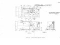
PHYSICAL DESIGN
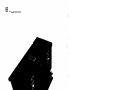
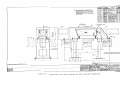
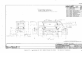
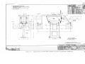
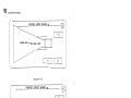
The DR-40 Radar consists of two main assemblies, a weatherproof
enclosure and a subplate assembly. These are shown in Figures
1-1, 1-2 and 1-3. Cabling is terminated at an AAR terminal
strip inside the DR-40 enclosure. A plug connector cable
connects the AAR terminal strip to the DR-40 subplate assembly.
..-
The DR-40 Radar enclosure is constructed of steel sheeting to
resist damage by dragging equipment. A non-metallic plate
forms rf window which allows the microwave to pass through
while shielding the electronics from dirt and the elements.
The DR-40 Radar is av~ilable complete with any of three
mounting bases: N451127-0201 for mounting on a cast iron
foundation and N451127-0202 for mounting on a concrete
foundation and N451127-0203 for mounting on two cast iron
foundations (see Section IV for details).
The subplate assembly forms the composite electronics package.
The subplate is composed of three primary sub-assemblies:
Antenna-Doppler module assembly, radar P.C. board, and mounting
plate. Details of these items are shown in Section VIII Parts List.
0
)
6015, p. 1-1
EEJ
UNION SWITCH & SIGNAL
Figure 1-1.
6015, p. 1-2
DR-40 Weatherproof Enclosure
UNION SWITCH & SIGNAL
ffi
l
/
,
Figure 1-2.
DR-40 Radar Subplate Assembly
N451128-0801
6015, p. 1-3
UNION SWITCH & SIGNAL
1
............... ""'"t
lt~···
Figure 1-3.
6015, p. 1-4
DR-40 Subplate Assembly Mounted in DR-40 Enclosure
I
j
UNION SWITCH & SIGNAL
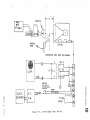
1.3
ro
\JJ
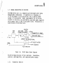
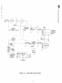
GENERAL DESCRIPTION OF CIRCUITS
The WABCO DR-40 unit is a complete self-contained solid state
doppler radar transceiver. It operates on a frequency of
10.525 GIGAHERTZ (10,525,000,000 Hz) with a nominal power
output of 75 milliwatts. Power requirements for all active
circuitry in the unit, are provided by regulated power supplies
which operate from 117 VAC, 60 Hz power lines. Following is a
block diagram of the DR-40 unit:
POWER
SUPPLY
SCHOTTKY
GUNN DIODE
DIODE
(TRANSMITTER) (RECEIVER)
ANTENNA
TRANSMITTED TO TARGET
REFLECTED SIGNAL
117 VAC
RFK
DOPPLER SIGNAL
,---''"---'--~
CHECK
SIGNAL
>----+-----
TO VELOCITY METER
> - - - - - - - - - - - - - - -'"1_,r---L--+ RFK INDICATION
AUDIO AMPLIFIER
Figure 1-4.
)
DR-40 Basic Block Diagram
The DR-40 Radar consists of four sections: transmitter,
receiver, audio amplifier, and regulated power supply.
1. 3 .1
Transmitter Section
The transmitter section contains a Gunn Diode Microwave
oscillator which oscillates with sufficient rf power output to
provide a one step conversion from de to microwave energy,
therby eliminating complex circuitry. The diode opertates
through a negative resistance caused by transfer of electrons
from a high mobility band to a low mobility conduction band.
The signal is fed to the antenna through a waveguide. A
ferrite circulator, located in the waveguide deflects a small
amount of transmitted energy which is used to bias the mixer
diode of the receiver. The deflected signal serves as a
reference frequency in the receiver.
1.3.2
Receiver Station
The receiver section is located in the portion of waveguide
that joins the Gunn Diode microwave source to the antenna. The
detector is a Schottky Barrier Mixer semi-conductor junction,
which is hermetically sealed in a ceramic case.
6015, p. 1-5
83
UNION SWITCH & SIGNAL
In operation, microwave energy transmitted from the antenna is
reflected from the target and enters the receiver waveguide by
way of a common antenna. This return signal is mixed with the
reference signal, providing a Doppler frequency equal to 31.4
Hz per M.P.H. The resulting Doppler/audio frequency is applied
to the audio amplifier section.
Audio Amplifier
1. 3. 3
The audio amplifier receives either the Doppler signal or a
precise 784.7 Hz check frequency from a frequency standard.
Either of these signals is amplified, limited and are outputted
to the velocity meter.
The amplifier passes a Doppler signal when a check signal is
not present. When a check signal is present, the Doppler
signal is shunted and the check signal passes. This check
signal is used to assure that the audio amplifier is operating
properly.
In addition to the audio amplifier, the printed circuit board
also contains an rfk voltage controlled oscillator check
amplifier. This circuit provifes a negative de output when the
Gunn Diode is providing microwave energy to sufficiently bias
the Schottky detector. This signal assures that the Gunn Diode
and detector diode are operating properly.
Regulated Power Supply
1. 3. 4
The regulated power supply provides all the necessary operating
voltages to the various electronic components, and is normally
operated from the commercial 117 volt A-C, 60 Hz power lines.
It should be noted that all input and output signals to the
DR-40 radar unit, are isolated via transformers providing
complete electrical isolation.
1.4
THEORY OF OPERATION
Velocity measurements, which are made using the Doppler
principle, rely on a shift in frequency that occurs when a
radio signal bounces bff a moving target. The frequency
difference between the incident and reflected signal is
proportional to the speed of the moving object. If the
frequency of the reflected wave is higher than that of the
incident wave the object is approaching. If the frequency of
the reflected wave is lower the object is receding. However,
either condition produces the same difference-frequency at any
given speed.
6015, p. 1-6
UNION SWITCH & SIGNAL
ffi
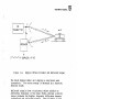
F
cw
~v
TRANSMITTER
F
00
RECEIVER
1
( ~ F DOPPLER =(F -F))
Figure 1-5.
Doppler Effect-Incident and Reflected Signal
The DR-40 Doppler Radar unit employs a continuous wave
transmitter. The return energy is detected by a Schottky
detector diode.
Reflected signals from a stationary object produce no
difference frequency in the mixer diode, whereas a moving
target produces the Doppler frequency difference between
transmitted and reflected signals. The following is the
mathematical formula for this phenomenon:
Fd = Ft
c + v
c - v
- Ft
2V
-c- Ft
WHERE:
,,-
Fd = Doppler frequency in Hz/second
Ft = Transmitted frequency in Hz/second
v = Target radial velocity in M.P.H.
c = Speed of propagation in M.P.H. {6.714 x 10⁸)
In the case of DR-40 Radar units, operating at 10.525 GHz, the
following calculation can be made:
'
)
FREQUENCY OF DOPPLER PER MILE PER HOUR=
{10.525 x 10 9 )
2
Fd =
(1.86 x 10 5 ) {3.6 x 10 3 ,
1
= 31.4 Hz/MPH
6015, p. 1-7
m
UNION SWITCH & SIGNAL
1.5
GENERAL SPECIFICATIONS
PHYSICAL
Dimensions Complete Unit
Dimensions Subplate Unit
Weight Complete Unit
Weight Subplate Unit
Operating Temperature
Range
28"L x ll"W x 12-7/S"H
15-3/S"L x 7-3/8"W x 7-5/8"H
44 lb.s (housing included}
10.4 lbs.
-4ooc to +7ooc (-40oF to
+160°F}
ELECTRICAL - RF OUTPUT (FCC Data}
Operating Frequency
Frequency stability
Spurious Emission
Power Output (rf)
Nominal Range
Type of Emission
10.525 GHz+/- MHz
+/- 0.2% of Assigned Frequency
No Emission Greater Than -44 db
Over Entire Frequency Range Except
At Assigned Frequency
125 mW Maximum (50 mW Minimum)
150 Feet
Continuous Wave (A~)
ELECTRICAL - SIGNAL VOLTAGES
Doppler Audio
rfk
14V p-p (Limited) into 500 ohms
Greater than -1.0 VDC (-.2V Mixed
Bias) into 500 ohms
Check Signal Required
ELECTRICAL - INPUT SUPPLY
voltage
Frequency
Power Consumption
95 to 125 VAC
60 Hz
12 to 14 Watts
\
')
6015, p. 1-8
UNION SWITCH & SIGNAL
'
")
ffi
SECTION II
FCC LICENSING REQUIREMENTS
Because the DR-40 Radar Unit is capable of emitting a signal
into the atmosphere, it may not be operated or maintained
without the applicable FCC License. This includes the station
license and the individual operator's license. Any adjustments
affecting power or frequency must be made by, or under the
direct supervision of a person holding a valid Second Class or
higher commercial radio-telephone operator license.
Application for new or modified station license can be obtained
by writing the nearest FCC field engineering office. Request
the following forms freom "Engineering-In-Charge" at the office:
NOTE:
FCC Form 400*
Application for Radio Station
Authorization in the Safety and
Special Radio Services
FCC Form 400-10*-
Instructions for Completion of FCC
Form 400
WABCO DR-40 Radar has been FCC Type accepted.
COMMISSION FIELD ENGINEERING OFFICES
HAWAII
NEW YORK
Honolulu 08808
Buffalo 14203
P.O. Box 1021
New York 10014
ALASKA
ILLINOIS
OREGON
Anchorage 99501
Chicago 60604
Portland 97204
P.O. Box 644
CALIFORNIA
LOUISIANA
PENNSYLVANIA
San Diego 92101
New Orleans 70130
Philadelphia 19106
San Francisco 94111
Los Angeles 90012
COLORADO
MARYLAND
PUERTO RICO
Denver 80202
Baltimore 21201
San Juan 00903
P.O. Box 2967
DISTRICT OF
MASSACHUSETTS
TEXAS
COLUMBIA 20554
Boston 02109
Deaumont 77701
Dallas 75202
Houston 77002
MICHIGAN
VIRGINIA
FLORIDA
Detroit 48226
Norfolk 23502
Miami 33130
Tampa 33602
WASHINGTON
MISSOURI
GEORGIA
Kansas City 64106
Seattle 98104
Atlanta 30303
Savannah 31402
P.O. Bocx 8004
ALABAMA
Mobile 36002
*November, 1971, or later, revision.
6015, p. 2-1/2
UNION SWITCH & SIGNAL
ffi
SECTION III
INITIAL INSPECTION, TESTS AND ADJUSTMENTS
3.1
INSPECTION
Upon removal of the DR-40 from its packing carton, examine the
housing for ahy impact damage or loosened fastener hardware. Then
unlatch the cover and examine the chassis for any indication of
internal impact damage, loosened or completely separated components,
damaged wires and broken or loosened electrical connections. The
radar must not be placed into service until any such problems have
been remedied. If the damage is not reparable in the field, or the
repair not authorized, the radar unit should be returned to the
manufacturer as shipped.
(Any unit being stored or reshipped should
be kept at temperatures between -40 F. (-40 C) and+/- 160 F {+70
C). Consult Section VII of this manual for repair information.
3.2
OPERATIONAL TESTS AND ADJUSTMENTS
NOTE
Prior to being placed Tnservice, each rf unit must
be checked to determine that it is maintaining the
proper frequency (10,525 MHz). This frequency is
the same for all rf units, although each installation is assigned a different call sign. The frequency must also be rechecked at regular intervals
{refer to Part 93 of FCC Rules and Regulations for
the applicable information).
3.2.1
General Remarks
This test of the DR-40 Radar unit requires removal of the subassembly chassis from the protective enclosure. Go to section
6.1.1 for the required steps.
3.2.2
Frequency Measurement
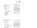
3.2.2.1 Test Equipment (Or Equivalent) Required
Frequency Meter, Hewlett Packard, Model X-532B
Analyzer, Simpson Model 260
Standard gain horn, Narda Model 640
Adjustable detector mount, Hewlett Packard, Model X-485B
Crystal, 1N23BN or 1N23C
Thermister Mount, Hewlett Packard, Model X-487B
Associated Hardware for Assembly
Power Meter, Hewlett Packard, Model 430C, or equivalent
.,
)
6015, p. 3-1
UNION SWITCH & SIGNAL
3.2.2.2
NOTE:
ON SITE FREQUENCY TEST PROCEDURE
The 2/56 Set Screw located on the Gunn Diode is pre-set
at the factory and should not be adjusted in this part
of the test.
1.
Apply operating voltage to the rf unit under test.
2.
Insert 1N23B crystal in detector mount and attach standard
gain horn antenna (see Figure 3-1 below). Use coaxial
cable, such as RG-58, to connect the Simpson voltmeter to
the circuit.
~ SIMPSON
260
NOTE 8ARREL OF F'REQUENCY METER MUST
8E IN THE HORIZONTAL POSITION
SHOWN WHEN MAKING MEASUREMENTS
DETECTOR MOUNT
Figure 3-1.
6015, p. 3-2
FREQUENCY
METER
STANDARD
GAIN
HORN
Frequency Measuring Test, Portable Set-Up
UNION SWITCH & SIGNAL
.
3.
Place horn antenna several feet in front of radar unit.
Set frequency meter for 10,525 MHz.
4.
Turn adjustable detector mount until a maximum indication
is seen on the voltmeter d-c scale.
5.
Adjust frequency meter for a maximum dip on the
voltmeter. Read the frequency directly from the frequency
meter.
This test only indicates the operating frequency and that the
Gunn Unit is functioning.
It does not check the amplifier
operation •
-.
If the DR-40 Radar unit does not fall within the specified
frequency tolerance, proceed to Section VI.
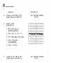
3.2.2.3
SHOP MAINTENANCE PROCEEDURE
OPERATION
VERIFICATION
1.
Arrange a test setup as per
Fig. 3.2
1.
2.
Adjust R36 5 turns clockwise.
2.
3.
Apply 117VAC .±:,2 VAC to Amp.
connector pins 5 and 12.
3.
4.
Connect a digital voltmeter to
TP5 and common to TPl
4.
Set digital voltmeter to
DC Volts and Auto Ranging.
(Fasten #3)
;
5.
Inspect operating voltage
marked on Gunn Diode Oscillator.
5.
6.
Adjust R36.
6.
7.
Allow DR-40 Radar Unit to
7.
stablize to operating temperature.
Should require 10 minutes.
8.
Inspect frequency of Gunn Diode
Oscillator as indicated on
HP532B frequency meter.
8.
Frequency should be 10.525
GHz+ 1 MHz.
9.
Adjust "FREQ. ADJ" screw if
required.
9.
When the frequency is 10.525
GHz+ 1.0 MHz, seal with
inspectors laquer.
Operating voltage of Gunn
Diode should be+ .1 volts DC.
Seal pot with inspectors
laquer after adjusting.
6015, p. 3-3
ffi
UNION SWITCH & SIGNAL
DEMORRAY BONARDI
HP-430C
0
X-487B
DR-50 RADAR
TUNING
WAVEGUIDE AXIS MUST BE PARALLEL
Figure 3-2.
Frequency Measuring Test, Shop Set-Up
3.2.3
RFK Adjustment
3.2.3.1 Test Equipment (Or Equivalent) Required
"i
/
Fluke 8120A-01 Digital Voltmeter
3.2.3.2 Procedure
1.
Connect voltmeter negative lead to the anode and the
positive lead to the CATHODE of the 1N759A Zener Diode
located on the Gunn Diode transceiver module.
2.
Apply operating power to the DR-40 unit.
3.
Allow a 10 minute temperature stabilization period.
The detector bias shall indicate -.4 VDC on the digital
voltmeter assuming little or no movement occurs in the target
area.
This voltage can be varied by unlocking the 2/56 nut and
adjusting screw located on the Gunn Diode transceiver module.
Make certain to retighten the locknut after adjustment.
NOTE:
ANY MOTION OR OBSTRUCTION IN FRONT OF THE ANTENNA
WILL ALTER THE INDICATED VALUE AND RESULT IN AN
INACCURATE CALIBRATION.
3-4
UNION SWITCH & SIGNAL
ffi
SECTION IV
APPLICATION, INSTALLATION AND AIMING
4.1
BASIC APPLICATION CONFIGURATIONS
The DR-40 Radar Unit may be installed adjacent to or between
the rails.
Install the DR-40 Radar as indicated by the proper
application drawing shown in the table below.
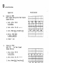
Table J:.
WABCO
Part No.
Application Guide
Application
Foundation
Figure
Number
Drawing
0451474
sheet
X451474-0601
Outside of Rails
Ballast
4-1
06
X451474-0701
Between the Rails
Ballast
4-2
07
X451474-0801
Between the Rails
Concrete
4-3
08
X451474-0901
Between the Rails
Ballast
4-4
09*
4-5
02
--
Wiring Configuration
--
i
i
*Two cast iron pylon bases used.
6015, p. 4-1
CTI
0
......
.
U1
"O
,!:>,
I
N
Gage Line
0
::aI
F-'*-J
,-,
0
::a
Pl
a.
7
178
·,.
.c:,.
EE
Prepared from drawing
0451474-06, Rev. 3
l'OPOF-IL
'I
:c
ll"
(II
15
z
)>
....----~~ ·-:r .... _......,
~,:------1·.
.
~
:x:,,
r
M«l
!!!
............
"O
"O
:. -: -.
r
.
-·-.'-T
_______ J
"°>
....0
......
I
31--j tr'
'+'
I
'+1 'T' ,
'/
Pl
....
rt
AAR Terminal
Strip (8-way)
0
:::,
0
c:
TIE TO 8£
l'1j
CUT 'II)
s
~
,_,
-lcO
°'"''5.
..."'
rt ....
{I)
I.Q
.... c:
a.~
(D (D
-t,t
=
0 .c:,.
HI I
::a
......
..........
Pl
..
{I)
)If
w
Pl
......
......
L
Pl
(I)
rt
l'1j
0
c:
:::,
a.
z
i::::j
0
.\
Pl
c
z
0
.........
Pl
rt
-Sj
'"
~
...
17i
..-!
SUK ELEVl'ITION
&nTTINf> PftOVIDCD FOi\ 2"HO!>t.. cir..'Tot1~'10$Ut'OLY
~ LENGTH O f " ~ lOPl'OTltCT HOOIC•UP
CIIBLC. Of'CN ENO OF HO'S,£ 'lO l!IE SEALED WITH DWCSltAL
OR EQUIVALENT. FOR C.O.,NEC.TINr. HOOK-UP W1a1ts. Sitt:
....
0
:::,
~ - 04.51474-Slt.O&.
' '
UNION SWITCH & SIGNAL
-
DUCIIPTIOII
&
EB
Fl4!iil1.l ( £
FITTING PllOVl't>E't> FOil 2 INCH I-IOSE.
CO~iOt<'ll!.ll "To SUPPLY APPllOPl'll'"TI!. LEIJ.,.TH
OF HOSE TO PllOTl!.CT HOOK•UP CABLE.OPEN
l!>lt> 01' H051! "To"BE 5EALl!D WITH DU><;51!."L·
OR EQUIVALENT.
FOR co1J1.lecT1iJ<o HOOW.·llP Wllll!.S see
1:>VJ<ii.
FOIJl.tD,..T\~
,CIIG.&1r.
RAt'\P
Ol4Sll"ll( 11
CO\J&-R
0(4511~., ...
D+Sl474·~H.02.,
5<.A.,~•1.·~ ~a•.u.P.C.ti.P
W~~U., 't".5.l'L. C. Pl.,
!cR-!4 •ZO k J Ila,< :inUP
WSHR-ltSTL Pl.AT._
1
ws,ul- /4:!ITL ""'"
-
1'4
.,
~-~(
TQPOFTII!
L--7
I ,/~/ lif'_I
-Ii..
f
1"'
L-..L____-
.,,_ \....- - -
v
~
=i'
\
---~
~
~<>:)
~--/~J.
s
I
,,,,,-,
(
, - - - ,
/~ \/\
loi\)T- 1/4•20 Httl< .TL
7
- ~--.
. ' / //II
!
Jl4!00z.
ST It If
;•2~,c
OF TP,ACK
4
5
I 1NTl!.IZIY11!.DIA•I!. TII~ ~
l1-......"'.!.'°
I',
!
x~
k?~IO'-O" , /
L_~_L_J
~\~~ . ~
If I I I .~i_J
2°><1'1°NOTCH
IN l>ffC:R.MC:PIIITf: TIE.
..
27-i;--------'----l-....
5'
f'IPPLIC,..TIOIJ OF Rl'l'DAR(ll,16\l>I!. llfllL•)
fOl'l Gl!.Nl!.-L IIIFORMATION 5££ 1>4!>1414·~,0I
2
2
n.!.
4
r
I.
1+
. · I
_
51 . L - - - - - - , - - - -4
)(451414·0~01
Ri.Tll.AC.U> IIJ Pl'IR:T FROr>1 Dioio05~·5H.14
~·=
l~ ii~iiiiiii ·.~: ~F.: !::~ E
RADAIZ, :OR--40
iF:Z({!f~T.:I-il~i~5~~iJJ? ;;:::.-;. ·;J~:.::£: ~~:.?:._ ~--:,;~-:- :~~
;..~!:\E~~T ::;:r..~.;,:{~t:.;~'. ~=:.:::'~~i~::~
• .,g
Wl:.TI-NOI.I•& •111 ........ C:OMf'-T
A80'/£ ...
:ti.. !
!: ,Qe !
0 ~~~.~::~:·;.~::~:::.~:·::·.~: ........... - · - '. .,_.__.
Figure 4-2.
Application of the DR-40 Between the.Rails (Ballast Foundation)
GEN ~/HE:~:~ ----·· ··-•~ ·-~ 12 4514 74
Q~
-
6015, p. 4-3/4
UNION SWITCH & SIGNAL
EE
,.:;.
DESCIIPTION
DIIMIIIII
t-
!!q!
N• TE C.
I 1· · 1,,e,
PROVIOED IO~
:! 1W ii 110·,1
(l1:..,TOM~R. --o :';.·t 1 PPLY APPl20PR1.qTE LELJC.,. ~t
2F HOSE TO "l<.CTE.CT -iOOK-UP
OP[>-, E.l<JD CF HOSE
TO BE ."?£ALEO WITH
J Ui<SEAL OR E.QUIVALEf.JT.
FOi.' C.01-JtJECTIWG HOOi<'.· UP Wli<f S
SEE DW6- L4SIJ 1 4 ·SH- 02.
C••BLE..
"III 41
l
IJl5109:d
4
lsc2,\x1l'1.HEX-CAP
»OLT, 1'1.x 3 SQ- STL-
4J.,E,4
SHIELl>, ~ EXPANSION l!>OLT
541350
477',-,
l</A5HER,~L.OCK (x.t!VY.)
NOT, ~ HE.)(,
---
12
J 47503
J '46.992 I
!IOLT, HAtJGEll
13
-r
J 500~
ScR-\/4-20><1 Hex STL CAP
14
J 47.501
WSHR·
II
i
OF TRACK
I
]
I
u
I:- ~---~-~ --~@,
;I
I
I
I·
1
'
I
//;
'
1
•
1 l:,
I ':
,
:r
'!'-.
; '.
I
'
I
; :
I
;:~0.L~
--,
·,N
LO
<J
l.~--t--:>,
r---
o:5__ --1
(,.
-------
/'---
--
.
L
d
,
L
Co-.1c.1U.TE.
,;.,;-
---
----...__ _
---:::-=----=-~
-
Foe»o OT•O"
'"'
rli\-i
---1.
r--
[
!. __
144
I
,--
3!.!
1
\ ,..____. ------- _ - - -
'
~
o
(.YLII.JDE.R
J /OXIO
I
---·-Ir'!~ -
7r--
3E!\"\!Ef:1w
'
I
__ \
I
/
>-'
/'I -- ----.=--'\' f
'
-.
- --',.
.~i - _
/1 __ - _ -:-1:
.l . ----r - - - --- - ..:i -- 2-.~, ·••
t:~ _,.
-,
--- 7
. -
-
=
(,
<
,d.
/
I
,, ,
')
~
I
AI\R
Nl.lT·'/4-ZO Hl!X STL
) I
/''/
I
--
~
1--
,8 ;,IA,)
1--
-----------
rH9Y161,
---
F:
-
~
,
I
.,f)7~;1
'
&
,, , \_'- .
i
.,,
_-- r1~ -
I-
iJ
IJDER Tll
--
·1
t_ll.\
: (
(
(//
1 --
t--
11.il
t--
I-
.--
------
I;-
!------·
~
~
- - - - _._!
=3:
----,
I
-
II
\
____J
L,W
B
-· -~I
-----
snuP
fERM11<.!AL
,;-2
·-f-
.--- .. \ < ///....__; i
1-----:,, . ?-:' - :..:::z'...J~
@)0
8
IG
;:
;--I,:_,
/ '/
- - 18 ,;;iTH - ~" ___' \
Ir
'
.if®JrJ
ii'--,---TOP
l~
' ~
(10 lJI
PLATE
WSHR • 1/4 STL LOCK
1 --
(4)
t":.,- -~ .
1-----;I
,
I
'/+ STL
15
I
.
i-'
.,/
~
WASHER,\'._ STL,PLATE
2.G
':::>IDE.
I;-
-
s,£
I;-
ELE.VATICN
I;-
APPLICATION 01' l<ADAR ( It-I ~IDE RAILS.)
FOR GIE.NS.RAL I\PPL1c ATION lt,1 F'OltMAT\Ot.J Sit E. :04514-,+~SH.0 I
IIJX4Sl474·0801
l'"l'"l 'l"'j'"l"'l"'l'"j"'l"'l"'l'"I
·,:>Q_Q','.)u<:.s..o ,..., Pl\11.T l'"IV,M ::,G,1oC5';'l-'.:)H,
'C:.
1
I
RADAR!.~R-40
l'AIIT NUM.[11
t--
~llllf•Tl(IN
"iiii.ffiililllutl'lllMll111Ultll
;:;.~~rfll:::~~- Mt't SIONS MU[ IN
)
~~ ~
;11"'
~1
0
----
[:I:~
":' .-;; '; ~·o
~:::,::;!!1:!:':i:.~
::::=::-:..-::
:,::.•::::.e:;:,:
::::£::·i~;E~f::~,
ntW.ll1t ..•••••..-ta11ru10:•1
r
"). '(" (I<...,
----·-
Figure 4-3
--~--·----·--
Application of DR-40 Radar Between the Rails
::-::;:::::.·::..~::::-;:;:";i
llf•• ..
1n•-•o••n•"''-'<ttl
APPLICATION &. CHARACTER.le-Tic DWtiS
INCHU
l~~~~~~~~~~~~====+==~~~r!o:R~~V~E~L!A~C::::D:R.=·=4=0=:R:A=D:A:R===1J
GUt OWG/NC:XT AHY.
1..,
~·ia ~
VI[ a, +I
•
,.-
••
ANGULAN OIMl'.NSONS :- ~
~ UNtON SWITCH I SIIIAl DIY,UIOI
.......,__,. ... c...........,,__,..
_..,_
0
On Concrete Foundation
f-f·l"
· ocft:
e1779
o 451474
08
U.&A
O!'
6015, p. 4-5/6
UNION SWITCH & SIGNAL
&
£
83
FITTING PROVlt)E\) FOR. 2 '' HOSE . C.uSTOME R TO .SUPPL'(
APPROPQ1A"TELENGTH OF H05E TO PROTEC.T HOOK-UP
CABLE.OPEN END OF I-IOSE TO BE SEALED wl"Ttt DU><5E.AL
OAEGlUI\/ALEN•. P'OR C6NNE.CTl,_.6 HOOK-UP WIR,E.5 SEE
"DwG. D'l-51474- SH.O~.
SET C.I. FOUNDATlON IN PLACE ON CENTER LIME OF
TRAC.K A5 INDICATED.
5CR- "(~.-IQ.ll ! HO M!> CAP
WSHR,- 1/!~TI. P~f'!'!'_
W6HR- 1/4 ~L a..c:ic;..._
AAR TE!lt~IINAL STRIP ( 8 WAY)
NUT- 1/4·20 HI.')(. 5TL
·TOPOf"RAlL
OF TRACK
"
4.
13
~--=----~
i
\F=(
.,
1·3'-"A.1R.E.A.
r:-_b=:=1
-IN
~
~
RAIL
\
L___
--{
_______
3
__)
L..__
"<!TOP OF TIE
l'llro
v
~---1
~
--. - -·
.r-- -- --:-.I_
''--. - -- !
l-2=
.,____ ----- ---j
- - - -,
-
L~~--::
_j
J J-t
r--~ -- .
b
•;.t
-l-----1-i
'-
,.,
7"§
-
(BE.TWE.E~lE.S)
1NTER.M.
..i-
-~
f-----t=J:J
~
. ~
-
, ·' , ,
.,..,
'
\OX 10
I
,/
/
"-; '
L\( y / .~ r-1
tL-'.".l~ ---
LL
h1r
,C~Ll~DE; Tltr-·
i~/;~?
l/
0
11
I
I
J
: ( I (//
i; I ) '
<1
.. lu_~JJu_iJ
--13l
·~>
;_~
:
I
I ' / /'
-~---SI+
~
L
1
~s
,t__j
J--·
------- 14 - - ~ - -
1
NOT RfCOMM£N9£D
FOR N£VV INSTALLiATIONS
1-----------17{------..i
SIDE ELEVATION
Sf£ 04!il474 SH.O~
APPLICATION OF RADA!l (tNS1D~ RAILS)
Fo~
"?'l.OUUC.li:.~ •ts) 9At!."T FQ.OM 'O l,,<oO 5 ~-'?\:!,I
iiu1 ..t•H,... n1·1.-1tiii-lil
G.~Hlii.12.SL RPPI-ICRTIO~. 1NF"OR.MIITI01'1 61t£ :t)~l+,-4-SH,01
MA1'1:RIAL/SPl'.CWJCATJl)N
1•
:::1':f:F...:a::-?,E'
~':':Z'-.:.'!:F.:'
IL.1::J
LCJ ::.. __ .. _11
*ml
tmP>.
... IS
=~==
..
·--·--·--
Figure 4-4.
Application of DR-40 Radar Between the Rails
GIEN OWG/M(XT ........
!
•1•tn"'1•1TI--II•-
;~ :.: -:~.:.~-:.:,
11 =.::.=:::.:..-=.s
,11n••------•
0
APPUC.ATtON Ex"..:~HARN:Tt~15TIC..
DWGS. ~OR VELAC DR ..40 RA
f\
_,..,_.......
!:.ff~
.,...M•-·-·· ......... -·- -'-. •
• • .
·-·----
~-·· ~
On Ballast Foundation
-,«- D. 45147+
H
'i-flf.
01775
I""'\-,
,-.a
-
6015, p. 4-7/8
UNION SWITCH & SIGNAL
Qff£1{E•K E
1. DR.-4o
No [t-tl\51\q-oro, (mR. 6Au.11sr \<Ju..oict"io,.)
'2 . Sc.Ht!"ll\\lt D1P.:1R.l-.t'\ -0-'\Sl'Z38- 'S\,\
3. v-J,R.i~ D1".'.}R."M. - F~Sl\7.S ·sl\8
c.~(,jrT si"'IIOL
- -,
+.5 IE
I
T1>1BV\./'\·noN OF APPLIC..I\ ,1ots1 s
"J •lf"Of3.M.U1or-.l
l<Aol\R. U>l1T .PAR."1
~
•
c.
- - - - - - - - - - ...... -I
A
SIC,.fl, 1S,c..6 1TEsi- ,,,i,sT B
A. c~ilLE
~p1.ic,;\-ioN Dw3. Df\Sl'\l't·SI-\.OZ:.
So.c. - ELI. 51\11 OR·J\;o RI\OMl S'f!m'.""
~ - V'\51\°U S~-l!
8.
D~. 1'4:i1, ri stt 8
QuRcfiT Cc1/'ISS1s -
N4S 11r s-oioz
'"'""
Ile
,, 111 v A.~
111
I\\ f\A,A. TIQN\1tl ...1.
t
r.c..c.
':.1R11'
lLL
ilO so-.t~ ± \01o I l.o Ill.
lltlE -.IO,TH.E _.., 11.0-/ AC. A/\CI\Q.\.l>11r OQ,ws.100 <• .1/7 /ll1P.
o P.
/\ilOuT
tAfi4.Yi.tKj
ee
&
12. •• /'I V.A.
S,r.s,'-'T'I :
AIJ, T'fpE
,s AE'"11!\CT.O 1:o
TO Ttt~ ,',,l-n>1Nt, HOT "10 EU.e~D
[)A •
.l,O A/\01() filtQUt,,IC..,
"lo .,,/,;m;.-r,.\\::
povs11.R
to /ZS
MPROUt-'IICTt.L'j iDO
10,soo\:o ~ 550 MH~
EM1~S1ct-l wntt "Tt\i:: P-'(ll..
I ~
I .
M!LLlwllrTS.
·"i0°c.. -k, 1° c:. (-~o'Fto \(.c°r)
'\,lo,E: (\
1
f1mNC. PR<..J10ED reR '21t1c:.>1
~CSE. CcJSToMill. ,:o SuPPLj AppllOpP-11\,E
LE t-lC.1t\ OF t-\osE i.o PP.<:nE<.., t-100K- uP
C.~ll\£. Ol'E>l ENO o\' .ios, "'(0 BE 5~LE0
"'"" ov~SEIIL oQ. EQu1--II\\.Et,1T.
1' - - - - -
I
I '
'
' )(
)-\
,
/
I
I
t. -
I
-
,/
'
' I
'
- -
'
II, vJ~ 'J
l\t-lf'\\&lcL
Cooi.1£l::n:,~
P1t-J
S \G. /\ ~ I
s1(.. e ~ 'lo
sic;.. eo.....~~9
t-lco
'TE'IT
~
I
~I
A INl'LJT • \ o
-UST B :rt-il'JT- 13
L----------'
'2.
3
61( l;w,.,m
1\-
61()
Ct'i:l\\:l
h.
r - - - - - · IS
z.
1..1::.'i
TO BE "'\Ocll.l1i.D HIAAL,fL
,o
Rft.,L, i
,>1c..\
~.,.a,,J
,op
a,
A.1>.11.
.P~R. ,\PPwcf>A,I\TE.
i\ff>1.1<K\io>J
,o
~lll0S1tl\ENT <W J..i11
C~N i'IE I\C.C.0"-1("-< 51-\t:O 0'j LC<>SEN Ill<.
4, NuyS
, I
IOI
,~,
111
4 WI\S\\Ei<.S
()t-1 t,\O\JNTIHC. ;:e.n
Cf Rl'IDM< )lo.Nil \\,"1':.1>1<.. Ci( ·..c-,JER_ Dt-<1' 'cND OF \)tl1T urn1L
0
f"ll"1."E'- -re Rl\11.. ) 'iE\l:nc.1>.1. l'ICJJS-."'>EHT "'~"''-M:!LE. 15 :± \
LOC.""'(1:1:>
~S.Eo,.&.1es
IT ,s f>,1w,EO
·~ I
1\ I
i•I
l~I
'}l.
~- Not-11>1~1. R~l.lC.£ c.:-
::r
~
«
o
r
7
~
lj
ao
.
""
,:, <
~
7
'
;1 i
Rr.01,Q_
1s u() ,O
!sfUO 11z. !,.\"!,
ll.~OP.I( JN1T
~·····
5
I,,
'I
~C'-6l£
e
. I
''-.i"
'\J\E..J I\
;t?'-
f.
SJvJr:.
1-\o!l.rtctlTI\L. /\.,MING ~0Jv,"l .....€NT Of U>-1,T CAN SE f',(CCl'\P,..1S~tO \'i'j lOOolNC. 'c t-tou>1n...Jc. fl),,E. 60L,5
>,.o ~cnm.i<. vi.» ui-1,11. 1T ,s l>,,,l-lED Pl'IQO-,L<'Q.,',1L ,•"<N Qr:.,~\\n:P '\- eo~-.-s. 1-1011.rio>JThL ~ClJ\/sr ,.-.£t-lT
l>,sMU\l',LC "' j; t. 0 lroi< N~511Z1·0t()\
/>.,Nil:! 1° fol=t N .. s11rl-OcO?...
3. -J(il"11C.l»L t,._'°"'""•
,.,J() Tiii: 01.0 CIJEW'
t-\OO~BAAQ(<T~
I
91(.~ C.t.lllE
CLEI\R.
S\-11.0
51\LO
1. l<r>,ile.R
o,.;n-s
A>I'/
'w,RE Cc.Loll,, I ,AGS
Mt,.fiK'tO, ·
BK
.. '
-y/'\110~ \l~INC. Ej.\STIN(. ~-:10
..--------,-, &
1-J·'
/
1tlST...\.LEO A."T AMUlollll
~o.
l[l
~
;1
t)SEO "10 t-\(1\SuR.E ,II~ 'JELQC.\Tt
!'/
~~
~"-
()u,Pu"T IS
0
°"fe'...,f'. ~I\M(,,E:
11--
&ysnM
.t.o'.luS'IMEttT ()\" Ta-It:
DR· '\0 15 Co>lER.EC>
SEll.-.1\c.E NIA~l) ... L. (.015.
DR·'\D ,a >loQMP,LL'/ N>!>L1.0 As \JI.AT CF A. Sl'E-W CoNT~\.. ':i'jfm"I"\ IJ~EO 1...i ll.MLA.oAO
C.\.M.-.1f\u.T10tJ 'fAP.D'i • -n\E 'o()Eu> Cl:>N~O~ S ' j ~ 0ET£<:.TS "Tt\E· App'l.OAC~ \NC.
CAP- ~ Jl\\'j)LIE'i 1"1\E P.EO.UESTEO -.IEL0<.1"T'/ TO "l>\E Sf>EcO C:oM·fQD1.. AMf'Llflll:R ~\tlllf,TES
,><E l=t"OM>.. "Ill STC.R:f "'\Otlm>"'-INC. THE C"ll.S I.CW_..L .JELOt.rf'./, -n\E l'\i,.OAA, OUTl'uf
s,r.,~l,L 01'" 31.1\ \\?; ~al. t,\l'l-\. 15 I.PPLl(O ,o-n<E -leu,<:1TjltJ1~£Q,,. ,HE ,J8Jlc.rt'{
....~('.o>l.'1El\.,S T"E At.0,.Q.O\JTPUT "ltl A Oto iD -I.De. out:NT {o-"t..J= IMP\-\) Tt\AT"
,, Appu'il:> To Tl4E Sp£EO C.Otffll.O'- AMPLIFIER. TllE speco c.o'~tt>OL 1'Mf>. Cot-lfARES
"TI\E A~t.$1EIJ "E..OOT't "TO ,t\E ,t..<:T""'~ 'IEI-OC.r1'')' At..10 £t-lill.(;\?ES AoJ AIA_ ~fiLl'I'/.
$
">I OllllvST Ai.LA'/ IW~I\S\.. ~ Oil. OECll.1:J\StNC. ,I\~ 'At~ "Pf>LIEC. "To T~l: ~Ell
f<:.11. 0\'111<\\lt-\ Ol'<l\t.110N ~ Mt-'1.111\\lr,/\ '3E>ls.rr,-.lfl'i, /t~OIO O,l!ITALJ..\>I<. OP.·'\o tll:Nl. sl1\otJC.
llQO-"IIC.I\S"'( '>Tf\TION ,o,,a:RS l Nco.l ~l~>J' I \.IE"!j P,,1>1£1<. LINES OA. IN C.Er.lEW-,\..
>,JI\IC.~ \\P,-.IE NOIS'j 8\lohD(."ST RM>to P.t.ttpT\OM. 1
tJ\1>111<\llM ">-rr.e ''-'"''/ '>\.\ r,.L'- e.,;:
FAec;,.l£>1c."j rowlR. 0...nPuT: "Tt\t a,.io
1! "" R~OtOLOC).110>1
S'fS1bA.5 O{>S).J>m>-1c. Tl>I.ETKal. ':>EE Q£1124:>flT OP.I\Wlwc. N-~·l!,lf s~. 15 1 i...ic
'!. 0.1.")o 01' \O,S1.5 MW!· 1. \.OS M\>'1,Q'-'110
J .. ,T
/t
s
rc,wi.Q. Q.<Q,llll.~N\f.t.11~:
OoPP\.ER l<ADMI.
Cf P,I\\Lwl\'J -l°i'.I\\CLtS P,T '-11111.\0VS fo1>115 A~otlC. 1 HE \<IIILlloAO ~Ii"""'/· DR·'\O IS A
""DI\R 1AA>IStE1-.IER. VTILli.lHl> co..int-11.lo-is vJl\'11: (J\~)IE,-\\55\0N AT 1qsz~ MHC.
W ITtt I\ W.t>\O f"-EQJENC"j p,.,,1(1<.. Ocll?.n" OF APf>l'.OJl.1 M"""'!:Y ioo MILLIWl'lrts.
DQ-'\o <:l\t,l eE >'l:)ulEO IN <. ITl\i:R CQ.·30 <>R OQ- -\0 tlUsn'AD!>I' \ " ' ~ CMe;s •
TtlE tl>.SE IS MOLIHT£0 IN "'CHE ll.l\lLAOl,0 ,Rl\<:l<wA'J OQ. w°A'/SIDi: AT A. po1t4T WHEQ£
'iELOt.n'I l"IEP,sollEME>lT \~ llE51"-EO. ·n\E Ql\ll\0 1'11.lr~lll'.,l<:)' o<J"TN"T Or Tt\E Oi:l.·'lo
,~ 011lECTtD PAll.l.Ll.£L TlYTI\E AA1l';I ,. .. o lioAl?:Ot-lTAL "lO <;.ll.MlE lE,lcL. SOME s .. ftLL
I\MQ\JNi C>F -IUl:nc"L (±1- 1 dEjO.EES) \ \\oQltOIITI\L ( :?(. ~E,11.its) AOJu~t'IEtIT IS
l)Ell.t'\l'\"TEJ) Y>'j "'CHE ....o.J~lll.C. AND Tt\E Eff&"{\,11:. ~~ Foe>.. .JETo<:.tr'f f,l\t:Mull,'.MblT\S
"*1\.01'1!<11\rf_Li \50 f£t.t.
•
,HE ClltC:Unll--j OF ,HE OQ-J\O \S 0.SH.NEtl , o B£ fltm'I MEC\\A~~"U.'/ 'i>ID E\.ECtlllCAL\.)'
C.OMf>"-rlllL°i: W\Tt\ Dll.·3o \>,!'>TI\U..lfflONS! :IT \ S llt-lT!ctf'K\"E'D TliJ'q ~E OA·.o\O WI\.~
Ql>JJAR \lNIT l'-IUST
"'1rrK cuRR~,
~Ll\.fS
Qt./.uL,o..T1..i1
PPIII.T en ... ALL .......~s .
"THE REC.Ll<.lrti\) 11::>-..iER. Suf,f,L" pQo.JIOES I\LL ,rt£ N(C£SShQ1 opc'l,,,,,1~ -JO\.TA<.£5 Foll.,
"1rlE ~hP.IOU > El.lC."10.o..l 1'- CoMpo>lE>ITS (. 1, IJ<>'t>AACL'/ Of'<iV1l£O \'~ti\ TIIE
CQN1MEil.C.1h\.
\10\.T -9owtQ.. L1tlES.
\tlPvT h>JO 0"1PI.IT S"tll\LS ,o T\1E
(lfl. 11.o, 1\1>.E 1sou;n1> "1111'\ -rll~'1S~o0.... fll. ,~<>I\Ol'lC. c.c,-.1.pLE1'< li:I.E(:t9.ICl'll. \SC>L ...TI0'-1
Po-;JER"
f,,,. N,1tl1N,u"'- "25 vl!>m
CH).,l<P.C.,Ell.l':.TI(
°""'f'l i
NmE: DR--\o
111,11. So,.:..nro
1W1~1"EP
APPl.1(~1" IQ.i:,l .
c.£~•!!.A.L :ItiForu,\lfflON
0R·4o
d
l'l\',-i_lNIUU\ '>l~tl~L lm,,JJ~ON icdb
(. "\,O..'l.1N,,JI./\ 0.c_. L ~ 1<£~\!'11'>1<.\:: !,<~O O•N\i
1511.
'Si
'
. 'Ev. Sl\1Z. OR·I\O QI\DM>.. P.c..S.
SEO.,.j\C.E N\"->lVll,L - SN\ l.o1~
7. G,ll>l,.(V,oot: C11us,s tH 5 \ltl-oio I
8.
····-·-···-·--
~
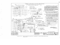
'j._-"tSl'\1'\·0\.0\ D~S\'\11 Ob OuTs1oe: of Q111LS BAl\11¢
'#..'t5l't1't·o101 Dist.o\11\: 01 8En/EE"1 l<All.'5 B~llr.si
MS\ "t7'\ · 0101 O~SI 41'\ O'o 8tTWE:EN Ql>.ILS .Co...ic!lEJE
c~aLE REQ·J,ll,£M£tHS
~
No. I D..,C\.
REf.
Nl\5117.l·OlOl {foll CC>l<:RETE" fb\l>llll\"ho.i)
\001
£l.:<:.1R1tP.L
~
83
~So >Et':T.
itJ~I
hh
c:: ·=-~:-: "~
I I
.1~
11
It
13
OR·.\o
CM1.e:PAR, #.REF. N+S1\Z.l!·l'\O\
~
I~
I I..
I 1
I 8
V1£..,J SttCWll>IC. ltll.1-,mlM..
ENO <:>I' C.O>ll'li:(1"DR, \':!..SE
D~ '\-0
lHI O,.aOIAhOJt 01' ' " ' (;JfllCUII ....... u IOU11'•
~.!~:t.:!~.:~===~~~.~::!~~,;~:;;~o,:!! EJ'lPE:~~::~·:
<;u11z.
.-,
l
'
;:::a~'\~~;:i~·
~::i:~!~~;c;~:~
•••H•
........ Moo ....1 AHD SIIMYU;c <Ol'tlU,1"10NI
6 ·-!: ! : It.::
i;l
C "'\. ~L
~ -:~~(il
u:a,,
j,._
,i11011 TO
Pl.ACID INTO NIUiUI.A"
EJ·l'5<\i:,\I
',I"\- <',O 15
SIGNAL " COMMUNICATIONS DIVISION
,.. ....... ~O .. U•••••Ol<04'GN0 .. Tl'm>O•••u.U ,,,..
rt::.;h;f_.;;;,
~·1·.1
!~·!"."~.!!.~
;;;;;-CN<<nO
'1{i_ - ·:;_;,_":j~
0(£
K
1'0"' !IWIIIJ>Uil
Figure 4-5.
DR-40 Characteristics
-~·=
)-(11.D.I\R
~N
i-r
tc-A{.,.... .~ ,~~ ' f l
CQu1PMENi cl\P,R,0.,C;TtR ISTl~S
t\wo
-o•••
SH, 1.4-
~d'f'L1<:..,,1DN No"'CES
WABCO SIGNAL A COMMUNICATIONS DIVI ION
'-./.A."v ...................,=••••rnmmM.t....
;-
•
I
a. .n .'-
,..,..NT'ftnN
.1. 5
Ne.ei.8
6015 I P • 4-9 /10
UNION SWITCH & SIGNAL
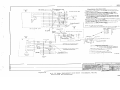
4.2
m
INSTALLATION
4.2.1
General Remarks
For optimum operation and maximum sensitivity, avoid installing
the DR-40 Radar unit near strong broadcast station towers, neon
signs, heavy power lines or in general, any areas which have
noisy broadcast radio reception.
It should be understood, however, that even when such noise
conditions exist, and a target comes into range of the DR-40
Radar unit, the output indications will be the true measured
velocity of the target, and the environments noise will in no
way be additive to the true target velocity.
Using the selected application method (see Section 3.2),
reposition and refashion ties, and excavate ballast, as
required to allow correct installation of the radar on its
mounting base to keep within clearance parameters. Make
certain that the modified section of track, as a whole,
maintains standards for tie spacing and ballast support.
Cable Requirements--SIG A, SIG B, TEST A, TEST B
4.2.2
a. Maximum signal attenuation shall not exceed 10 db at
1000 Hz.
b. Maximum de loop resistance - 500 ohms.
c. Cable - twisted pair, shielded.
4.2.3
Check Signal (785 Hz)
a. Maximum signal attenuation shall not exceed 10 db at
1000 Hz.
b. Total de loop resistance - shall not exceed 500 ohms.
c. Cable - twisted pair, shielded.
Power (117 VAC)
4.2.4
a. Cable - must meet all local electrical code
requirements.
b. Capable of providing a minimum of 25 watts at each AAR
Terminal Strip.
4.2.5
Power Requirements
Each DR-40 Radar unit contains all the regulated electronically
filtered power supplies essential to the operation of its
various electronic circuits. These power supplies are
energized via an internal isolation/stepdown transformer, which
is intended to operate from the commercial power lines. The
input power requirements for each DR-40 unit are 95 to 125
volts*, 60 Hertz and .1 to .117 ampheres~ Each DR-40 unit does
not require more than 12 to 14 watts operating power.
*r.m.s.
6015, p. 4-11
, ffi
UNION SWITCH & SIGNAL
Electrical Interface
4.2.6
All extertnal electrical connections are accomplished by means
of a standard 8-way AAR terminal block. This terminal block is
located within the DR-40 Radar enclosure as shown in Figure 8-1
on page 8-3/4.
After connection of all external wiring to the 8-way AAR
terminal block, interconnection to the DR-40 subassembly part
number N451128-0801 is provided by means of a cable assembly,
part number N451128-1401, which is provided with the unit.
See Figure 6-6 for specific electrical wiring assignments to
the DR-40 Radar unit.
Final Checks
4.2.7
a. Inspect all wiring tags and check that they are on the
correct AAR terminals on the DR-40 unit and on the
equipment room rack.
b. Check for loose AAR terminals nuts which would result
in intermittent operation.
c. Inspect for stray hardware which might short between
AAR terminals.
d. Check to see if cable plug connectors are secure and
properly seated both in the DR-40 unit and in the
equipment room.
4.3
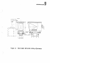
4.3.1
AIMING PROCEDURES
Horizontal Adjustment
The horizontal adjustment range for the N451127-0201 unit is
+/- 6 degrees. Adjustment range for the N451127-0202 unit is
+/- 1 degrees. To adjust horizontally:
1. Loosen the four mounting plate bolts.
2. Rotate unit until parallel with rail~
3. Retighten mounting bolts.
4.3.2
vertical Adjustment
The vertical adjustment range for all units is +/-1.5 degrees.
To adjust vertically:
1. Loosen the four elastic stop nuts or mounting feet of
the radar.
2. Raise or lower one end of the unit until it is aimed
parallel to the rail.
3. Regighten elastic stop nuts.
6015, p. 4-12
UNION SWITCH & SIGNAL
Figure 4-6.
VIEW
X
STUD
~
DR-40 Radar Horizontal Aiming Adjustments
1-13
ELASTIC STOP NUT5
/
~ADAR .;N1r
MCuN f 1N4' BRACKET
Figure 4-7.
DR-40 Radar Vertical Aiming Adjustments
6015, p. 4-13/14
"")
UNION SWITCH & SIGNAL
ffi
SECTION V
PERIODIC PREVENTIVE MAINTENANCE (5-6 MONTHS)
WARNING
AC POWER TO THE RADAR UNIT
MUST BE DISCONNECTED PRIOR
TO CONDUCTING ANY HANDS-ON
MAINTENANCE, OTHERWISE
PERSONAL INJURY MAY RESULT.
5.1
INSPECTION
Make a thorough visual inspection of all w1r1ng and cables for
evidence of fraying or burning. Also, test wires to determine
if any have worked loose at their connecting points. Check the
physical integrity of all other components, looking for indications of burns and cracks, leakage of insulation compounds
and general physical damage. Also, check the structural inte~
grity of the printed circuit board and the mounting tightness
of all integrated circuit packages. If any of the above
general types of problems are discovered, go to Section VI to
the appropriate maintenance section.
5.2
CLEANING
CAUTION
DO NOT ATTEMPT TO CLEAN P.C. BOARDS COMPONENTS
OR OTHER SMALL COMPONENTS WITH ANY KIND OF
STIFF BRUSH, SOLVENTS, VACUUM CLEANER OR COMPRESSED AIR, OTHERWISE DAMAGE TO THESE COMPONENTS MAY RESULT.
..
1.
Remove excessive dust from internal surfaces and components using a soft bristle brush and low-pressure compressed air j ~
2.
Wipe external surfaces with a soft, damp cloth to remove
foreign materials. Do not use any corrosive chemicals
which may be potentially destructive to the housing or rf
window.
3.
Reconnect ac power and replace top cover.
6015, p. 5-1/2
)
UNION SWITCH & SIGNAL
ffi
SECTION VI
IN-DEPTH CIRCUIT DESCREIPTION AND TROUBLESHOOTING
WARNING
TO AVOID PERSONAL INJURY, AC POWER TO THE
RADAR UNIT MUST BE DISCONNECTED BEFORE
TAKING ANY STEPS TO PULL THE UNIT FROM ITS
MOUNTING IN THE CLASSIFICATION YARD.
6.1
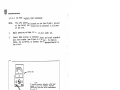
6.1.1
ACCESS TO COMPONENTS
Removal of Subassembly
1. Remove topside cover from enclosure.
2. Disconnect Jl connector, as located in Figure 6-1.
3. Using a 3/8" socket drive tool, remove 3 retaining nuts
on base plate, also indicated in Figure 6-1.
4. Carefully lift the subassembly chassis out of the
enclosure.
6 .1. 2
P.C. Board Access
1. Remove four hex head cap screws which attach horn and
Doppler transceiver module to subassembly chassis.
2. Disconnect wiring harness dress from chassis.
3. Rotate horn/Doppler transceiver module 900 away from
P.C. board side, as indicated in Figure 6-2.
3/8" SUBASSEMBLY RETAINERS
Figure 6-1.
DR-40 Disassembly Diagram
6015, p. 6-1
~
UNION SWITCH & SIGNAL
PRINTED CIRCUIT BOARD ,
T4
HORN AND GUNN DIODE UNIT
T1
I
I
J1
Figure 6-2
PRINTED CIRCUIT BOARD
)
7
T4
T 1
II
J1
HORN
AND
GUNN DIODE
UNIT
. /l
Figure 6-2
Relocation of Horn and Gunn Diode For Service Access
6015
I
P• 6-2
UNION SWITCH & SIGNAL
6.2
ffi
DETAILED CIRCUIT DESIGN AND FUNCTIONAL DESCRIPTION
6.2.1
General Remarks
.
Block and complete circuit schematic diagrams of the
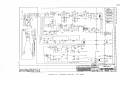
DR-40 Radar unit are shown in Figures 6-3 and 6-4,
respectively. Refer to Figure 9-2 for placement of
chassis components and 9-3 for printed circuit board
components (partrs called out on pages preceding these
figures). All electrical inputs and outputs are
terminated on a 16 pin Amphenol male connector mounted
on the subassembly chassis.
6.2.2
Power Supplies
Voltages:
(+)and(-) 5.6 VDC to(+/-) 0.5V.
Plus 10.5 VDC (Adjustable 8 to 12 VDC).
Minus 9.0 VDC +/-.5 volts.
The primary source of power for the DR-40 Doppler Radar Unit is
117 VAC 60 hz., which is applied to terminals Jl-5 and Jl-12
and to feed the primary winding of step-down transformer T-4.
The transformer primary is fused (F2) at one ampere. The
secondary winding is center tapped and the center tap is tied
to the chassis and serves as chassis and signal ground (TP-1).
The secondary ac voltage of T4 is rectified by 012 to Dl5 and
filtered by Cl9 and C20 to produce unregulated voltages of
approximately minus 17 volts and plus 16 volts de at TP-2 and
TP-3, respectively.
Regulation for the negative voltages is provided by the zener
reference voltage of Dll and the operation of pass transistor
Q2. This reference voltage of approximately 10.5 volts is
filtered by Cl8 and C23 and is applied to the base transistor
Q2 and produces -9.0 +/-.5 volts at TP-6 by emitter follower
action. The 5.6 volts supply is established at TP-7 by zener
diode DlO, whose output is filtered by C14.
Regulation for the positive voltages is provided by IC-8 which
is a Monolithic Voltage Regulator Type 723 used with external
pass transistor Ql. The voltage at TP-4 is adjustable between
8 to 12 volts by the setting of R-36 in order to provide the
Gunn Diode voltage with the range of voltages marked on the
Doppler Transceiver waveguide packages by the manufacturer.
The regulator output is filtered by Cl6 and zener diode D9 is
used to establish the +5.6 VDC output which is again filtered
by C13. Since the Gunn Diode is susceptible to voltage
transients larger than the recommended supply voltage, a zener
diode (D8) is used to prevent such transients from destroying
the Gunn Diode. The output of the positive regulator is fused
at 1-1/2 ampheres by Fl.
6015, p. 6-3
EE
O'\
0
.......
u,
c
z
z
i5
'"d
i:j
O'\
I
0
"'"
CALIBRATION
INPUT
//~
~ RECTIFIER')~,,
-·
f'.:: -,~ .
-i;=v_,,..."o
J:
QII
[P~
(/)
c5
z)>
r
CONTROL
DOPPLER AND
BIL AT ER AC
- ~:~.:~RAT.'_ON
INPUT. '\_SWITCH.,/ OUTPUT
f I~
FIE
.
_J
v\J
SHIELD
l
DRIVER
'--+--4-------l-~
BILATERAL'
SWITCH
AMPLIFIER >------1
INPUT
MIXER
OUTPUT
GUNN
DIODE
AND
MIXER
CONTROL
/
PYRAMIDAL!
HORN
-9
+8 TO
12VDC
AS NOTED ON
GUNN DIODE
BILATERAL'
SWITCH
V.J)c;
RADAR POWER
SUPPLY
-5.6
voe
- - -4'
r
;t
MULTl;VIBRATOR
+10
voe
DC
+5.6V
DC COMMON
Figure 6-3.
DR-40 Radar Block Diagram
"'---//"
I
CALIBRATION
OR DOPPLER
OUTPUT
UNION SWITCH & SIGNAL
II
lOPF
~
JOPF
Cl
IMfD
Rl6
Rl4
'
IOK
RIO
21K
HOK
±J,•~
FASt~.
I
II&
I
-t-10.5
... ... ...
;~.;
RO
s.11<
.-----,
.
2P
C24
IMf'D
••
CONTROL
.....
O i·~
R21
DO
IN4742A
Sit<
-
n
-,v +10.a,v
S.tK
5. IK
IOK
( I : 2)
cir
.,wo
1:t
TPZ I
.Y
C2:ASTr
+T
tMFD
,J&.cow £
J,l-11.\
)) ill§lf
IOOK
.JMFO
TPl4
(2 : I)
TPll
R>t
020
IOOK
1Ntl4
r-~~~~~>--~~-,-:,,'&.
~f~
ANC.h_
',-~
AAAJ!L
L~~~~~~~~~~~~~====================~~~==~~~~~~~~~~~~~~~~~~~~:
...
,. -...•. · ·~· I
c12l+
RlO
HK
IMFDT-
I •
-s.,v--~-<1--~~~~~~~-<1--~~~-+-~~~~o-~~~~~,~~~~~~~~~~~~~-1
TP3
"
Y
MJI
...
"'~I
,--- ,u,ru
I0.5V DC
I
)oj
Cl t
!
"''
1"
·= ,...p
1
000
RU
R35
UOA
l.O~
3300Mf'Dr
Rl6
2K
Rll
~-'!IK
I
.
---
v
IK
Cit .J..IMf'O
,1.+
l-
C23
.001
200MfD
r
~
,,,,..i' •
I
I
I
N01£:£
nm
DC SUPPLY
IN52l2
*
-s.1v oc SUPPLY
l'CI UN4stoss-uo,(F4s1ou-•2)
.
i'------1!
FAsTON #10
UC451238-1001
)
-
.""r.•
___________
_______
__.
L-------------
t~ .
I&.
~
I
MR.,h.
,)~
~,-,-··rr1n
.
~
Cl4 .1.IMFD
T~ST
I
TPT
010
I
I
. : IMFD
C 15 ..1..-
I
I
I
-
,;:u
DI
j~ ....
----------<L--------...- - - - - - - - - - 1 v
.,.
I
FAS TON 1111
. :, I Lil
DI
IN4742A
...
I
I
I
I
I
I
·I
••NA.L
~i::wo ._---+----+s.,v oc SUf'rLY
INSUZ
TPI
"
TP5
I
,.,.,. Ju..
rI
C2Z
RH
M- .lb.
J,1-•IJ.\
--'W'J'-----llR4
510
.J
"£ ,.,.,. J.L.
---:;?? 4.!.H II •,&
160P,
TPU
Rl
01000: UNIT
SUPPLlfO WITH nc
COIWOHfNTS BY
vt:HDOR.
#R:K
J our Fur
rASIOH #7
-s., +s.,
I
VENDOR-
I
R. .
R41
IOK
C(»fftECTOII OH .,..,
UNIT IUffPLIIED ••
_£ GUHII
1
I
I
I
I
I
TPI 5
-ov
A.AR TERIONAL ~OCK
LOCAT£0 WITHIN
RADAR (NC~OSU"I'.
I
CIO
sue-
I
I
250Pf'
TPJO
I
IN THIS St:CT IOM AIIII
,II&
~~
250P'F
COMPONENTS SHOWN
I
HOK
C21
4.7Mf'D
I&
J
CONTAUCD tN Asa'(l
ASSY .UH-451111-0101
r:w,i
IN4742A
021
uH•s1 u1-uo1
MOUNTED OH
'f:T ml'~
(DA-I)
CAlOlt
N01£5:
,............
I
BU
RI
IK
11::,.
EB
RADAR
)
( ENCLOSUll&
I
I
AAR_h
J • -·
IIJY AC
I
IK
~
J/~12
MR...Jb.
OR-40 RADAR U>I IT
TYl'f ,m VELAC CLASS YARD
~TAOOARO CIRCUITS
')
WABCQ
~
__...,...,~
-·-t:m'
MY--f'
_,
.;;;, lQ 451238
." ---
COGa ID•NT
~~'
UNltll SWITCII I SIIUI. llfflSNI
1001
- 1$...
....
Figure 6-4.
Schematic Diagram
DR-40 Radar
6015, p. 6-5/6
UNION SWITCH & SIGNAL
6.2.3
ffi
velocity Measurement Circuitry
The DR-40 has a single printed circuit board which utilizes
several types of linear and digital integrated circuits.
The printed circuit board contains a single CD 4016 AE which is
a COS/MOS (Complementary-Symmetry Metal Oxide Semiconductor)
Quad Bilateral Switch. Three of the four solid-state switches
on the single chip are used. Each switch is made up of an
input, an output, and a control connection. Whenever a
positive voltage or a high logic level appears on the "control"
input, the switch is in the "on" state and whenever the
"control" input is at a zero or a low logic level, the switch
is in the "off" state.
The printed circuit board also contains a COS/MOS CD 4001AE
Quad 2 Input NOR gate. Two of the gates are used to form a
multivibrator and the other_ two are used as logic level
inverters.
The DR-40 also uses five style 777 Operational Amplifier Linear
integrated circuits. IC2 through IC6 are used as amplifiers.
and line driver. IC2 and IC3 have amplification limiting which
is performed by a Beam-Lead Diode Array containing 6 matched
diodes.
The Doppler Transceiver contains a mixer diode which functions
as the receiver of the unit. The diode requires forward bias
amd this bias is developed by diverting a small amount of rf
output energy from the Gunn Diode. This is accomplished by a
fixed ferrite circulator located in the waveguide unit and a
2/56 adjustment screw marked "mixer" on the waveguide
assembly. The screw adjustment can vary the de voltage from a
-0.2 to -0.4 volts de at the mixer terminal. The mixer output
is fed to two parallel data processing circuit branches. The
first of these is the Doppler output and the second is the rfk
output branch.
The Doppler circuit branch input contains a resistor capacitor
network which loads and forms a high pass filter input to the
first solid state switch of ICl. The control input under
normal velocity measurement conditions is at a high logic level
and, therefore, the Doppler signal is passed without
alteration to the first of two identical ac amplifiers made up
of IC2 and IC3. The low signal level and low frequency gain of
these amplifiers is set by the ratio of R8 to R78 or Rll to
RlO, which is approximately 130 per stage. The diode networks
formed by the CA3039 packages perform a gain limiting function
by conducting on both positive and negative half cycles when
the signal output of IC2 and IC3 is sufficient to forward bias
the three matched diodes effectively in series.
These diodes, when conducting, shunt R8 or Rll and reduce the
gain of each stage. The capacitors C21 and C4 set the high
frequency gain roll off. The output of IC2 and IC3 is limited
to about 2.2 volts peak-to-peak under normal Doppler signal
input.
6015, p. 6-7
ffi
UNION SWITCH & SIGNAL
The linear integrated circuit amplifier IC4 serves as the line
driver.
It has a gain of approximately two and its output
contains back-to-back zener diodes Oland D2 for transients
suppression. The output level at TP-19 is about 5 volts
peak-to-peak. Rl5, Rl6, and C26 serve as loading and a low
pass output filter.
Transformer Tl couples the Doppler output
to the line, which is terminated at the monitoring location by
the velocity meter.
The second circuit branch, in parallel with the mixer output,
is the rfk branch. The rfk branch's function is to deliver, to
the monitoring circuitry, a DC voltage level that is indicative
of normal radar transceiver operation. The signal level at
TP-10 is approximately 0.3 volts de.
ICS is a amplifier with a
gain of about 59, so the signal level at TP-11 is about 1.5
voe. Two NOR gates of IC7 are connected to form a
multivibrator whose output at TP-12 is a 10 V. p-p squarewave
at about 11 KHz. This signal is applied to the control input
of the solid state switch ICl, which alternately activates
deactivates the switch. The output at TP-15 is essentially the
same level applied to the solid state switch input but chopped
at the multivibrator rate.
IC6 is an ac amplifier with a gain
of about seven.
Its output contains transient suppression
(diodes 04 and DS) and is transformer coupled to a diode
bridge. The de voltage developed by the bridge rectifier (016,
17, 18, 19 and filter C24) is applied between the shield wire
of the velocity output cable and the center tap of transformer
Tl. The de velocity is recovered at the monitoring point by
connection to the center tap of the transformer at the
receiving end of the line and the shield.
Upon installation, it is necessary to calibrate the velocity
meter at the monitoring point (obtain and refer to FCC Rules
and Regulations Manual, Part 90.). This is done by applying a
calibration signal of 784.7 Hertz to the calibration line and
transformer T3. This input contains transient suppression (06
and D7) and the signal is fed to both the input of the solid
state switch at pin 4 and is half-wave rectified by D20 and
filtered by Cl2 and activates a NOR gate of IC7. The output
without a calibration signal is at a high logic level, and the
presence of a calibration signal causes it to switch to a low
logic level (TP-14). This action opens the switch in the
Doppler signal input path and causes the output of TP-13 to go
to the high logic level, activating the control input of the
solid state switch at ICl - Pin 5, and applying the 784.7 Hertz
signal to the audio amplifier and line driver.
The calibration
signal is then applied to the line and delivered to the
monitoring point for velocity meter calibration.
6015, p. 6-8
UNION SWITCH & SIGNAL
6.3
6.3.1
ffi
TROUBLESHOOTING PROCEDURES
Preliminary Checks
6.3.1.1 Physical Defects
Check the physical integrity of all components, wires and
connections via Section 5.1. If damage or deterioration is
found, proceed to Section VII and the appropriate corrective
maintenance procedures.
6.3.1.2 Control Settings
Incorrect control settings can create indications of a problem
that does not actually exist. Check that all system controls
are set properly. {Example: Is power "ON" to the unit?.)
6.3.1.3 Associated Connecting Equipment
Make checks of the equipment being used in conjunction with the
DR-40, including that associated with the power source. Also,
check the physical integrity of all interconnecting cables.
6.3.2
Isolating a Problem Circuit
To isolate trouble to a specific circuit, note the symptom.
The symptom often identifies the particular circuit in which
the trouble is located.
{Example: If speed measurement fails,
but check reveals that the rfk voltage is present on Sig A and
Sig B, then the problem can be traced to the Doppler portion of
the circuitry.)
After the trouble has been isolated to a particular circuit,
check the Fasten connectors on the circuit board for correct
locations {see Figure 6-7). Faston connectors may be used for
circuit isolation.
6.3.3
Power Supply Problem?
Incorrect operation of all circuits often indicates trouble on
the supply. Check first for the correct voltages of the
individual supplies. If correct voltages are indicated, then
another component is causing the problem {which also can appear
as a power supply problem and thereby affect all other
circuits). Refer to the following table for power supplies
tolerances. If tests reveal a misadjusted supply, go to
section 7.5 {p. 7-4) for adjustment procedures.
6.3.4
Checking Individual Components
NOTE:
Checks described in the following sections for soldered
components are best conducted by disconnecting one end
of the component, so as to isolate it from surrounding
circuitry.
6015, p. 6-9
ffi
UNION SWITCH & SIGNAL
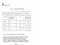
Table II.
Power Supply
Power Supply Tolerances
Voltmeter Positive
voltmeter Lead
Tolerance
+ 10.5 Volt
TP4-Unfused and
TP5-Fused
TPl
Adjustable 8
VDC to 12 VDC
-9.0 Volt
TP6
TPl
+/-.5 Volt
+5.6 Volt
TP8
TPl
+/-.5 Volt
-5.6 Vlt
TP7 '
TPl
+/- .5 Volt
6.3.4.1 Horn and Doppler Transceiver Module Components
Components of the Horn/Doppler Transceiver Module are analyzed
for possible defects via the complete substitution of the
faulty unit with another which is known to be in working
condition. However, disassembly for this purpose is restricted
to the externally mounted Zener Diode and Schottky Mixer Diode.
NOTE
The Gunn Diode unit must not be removed from
the transceiver module for any purpose. Doing
so would result in wide output variations and
therefore jeopardize FCC type acceptance for
the radar and the customer FCC station
authorization limits. Refer to Section 7.2.1
for allowed disassembly steps for these
components, and to Section 6.3.5 for allowed
troubleshooting procedures.
CAUTION
DO NOT MAKE OHMMETER CHECKS ON THE RF DIODES OR
INTEGRATED CIRCUITS DURING BENCH TESTING,
OTHERWISE DAMAGE TO THESE DEVICES MAY RESULT.
ALSO, THE SCHOTTKY (MIXER} DIODE IS SUSCEPTIBLE
TO DAMAGE BY STATIC ELECTRIC DISCHARGE. THE
TECHNICIAN SHOULD TAKE STEPS TO DISCHARGE ALL
STATIS ELECTRICITY FROM HIS BODY BEFORE HANDLING
THESE DIODES. THE DIODES, WHETHER OR NOT THEY
ARE SUSPECTED OF DAMAGE, SHOULD BE STORED ONLY
IN AN ELECTROSTATICALLY SHIEDED CONTAINER, SUCH
AS THOSE THEY ARE SHIPPED IN.
6015, p. 6-10
)
UNION SWITCH & SIGNAL
ffi
6.3.4.2 Diodes, Other Than RF
Diodes may be checked for an open or short by measuring
resistance between terminals. Use an ohmmeter with an internal
source between 800 millivolts and 3 volts. A normal diode will
show a high resistance in one instance and a relatively lower
resistance when the meter leads are reversed. Faulty diodes
will show high resistance in both directions (open) or low
resistance in both directions (shorted).
6.3.4.3 Transistors
Transistors suspected of having a defect are best tested by
substituting an identical one for it which is known to be
operating properly, then carrying out operational tests.
However, it is possible that a circuit fault at another
location caused damage to the original transistor and that the
same damage may be inflicted on the replacement. Carry out
other components and wiring tests if this latter situation is
suspected, or if the replacement transistor incurs the same
apparent problem as the original. If substitute transistors
are not available, use a dynamic tester {such as a Tektronix
575 or equivalent). Refer to Section VII for replacement
techniques.
6.3.4.4 Resistors
\
I
Check resistors with an ohmmeter, using Parts List to obtain
the correct tolerances for the resistors in question. Replace
only those resistors with test values which vary widely with
the intended value.
6.3.4.5 Transformers
Transformers are checked for an open or short/partial short in
the windings. Use an ohmmeter to check continuity for an
open. For shorts, check waveform response by passing high
frequency signals through the circuit.
6.3.4.6 Capacitors
A leaky or shorted capacitor can best be detected by checking
resistance with an ohmmeter on the highest scale. Do not
exceed the voltage rating for the capacitor. The resistance
reading should be high after the initial charge of the
capacitor. An open cspacitor can best be detected with a
cspacitance meter or checking whether the capacitor passes ac
signals.
6015, p. 6-11
ffi
UNION SWITCH & SIGNAL
6.3.5
Systematic Circuit Troubleshooting
6.3.5.1 General Remarks
The following diagnostic routine consists of a series of
consecutive subroutines which must be followed in the indicated
order. The individual steps describe actions to be taken with
the test equipment, ask for verification of test results and
recommend where to look for faults based on unsatisfactory test
results. Some also recommend how to deal with faults. In
general, it may be assumed that if a step yields a "yes" answer
to a particular question, or gives no special "go to"
instructions, then the routine may proceed to the next
consecutive step. When the word "STOP" is reached, a
subroutine has been completed. The proceeding would then
continue onto the next subroutine if no fault or variance in
test results is found. Note that "go to" instructions for "no"
answers to test results may take the procedure over to steps in
other subroutines. The technician should be careful to observe
variations in this general approach and to follow individual
step instructions carefully. A useful aid in this procedure is
to mark down the number of completed steps so that procedure is
followed in the proper order.
Immediately following the numbered test procedures are the
correct voltages and waveforms that should be obtained from
test points and terminals, as they are individually analyzed in
the procedures. The three immediately following figures (6-5,
6-6, and 6-7) are provided for orientation with the test
set-up, chassis wiring and Faston locations. Of course, use
the general schematic on page 6-5/6 for troubleshooting
procedures as well.
NOTE
Test Point 1 (TPl) is used as a common for
voltage measurements unless noted otherwise.
(Go on to page 6-16 for initiation of test procedures.)
6015, p. 6-12
16·~
NARD A
POWER
METER
HP-430C
X-487Bllj~532~j.---_640
r-
~~
0
-
~~I)
TUNING
FORK
~ ~
DR-40
~Li
WAVEGUIDE AXIS MUST BE PARALLEL
•
-----i A, _ _ _ _ _ _1_
IK
SCOPE
COM.
B'l
SIG A
2,3
4
c
O"I
0
r-'
ELECT ..
A. F.
COUNTER
GEN.
z
5
z
~
::j
n
:c
~
Cl)
U1
i5
z
:r,
.
'd
r
O'I
I
~
w
Figure 6-5.
DR-40 Radar Test Set-Up
EE
UNION SWITCH & SIGNAL
FZ
'
HJSE \
lA ·tSO'I(
I''1
·,-j
EXTERNAL VIEW
A.A.R. TERMINAL
:~1-:.-;;~~
:~:
r-,1 ~n
-02
10[!- l ._______________.. :_;. . .--©
L__
03
4
O
CONNECTOR
Jl
110
12u----
SHIELD
BLACK
BLACK
'•'
(ij#3
0
#4
r--il 5
'. 06
130- - - - " 7 - - - - - - - - - - - - - L - - - - - ' . 0 # 5
140
CLEAR
,,.. . . ,
r--7------------B-LA_C_K--------~,--:..,_~@)# 6
:;--o 7
150
1
o #7
~:_~8-=::.-1~~--:.-1'-
:,.,:
@#8
A.A.R. TERMINAL
BLACK
(-\
CLEAR
. - - ~ ~ ~ ~ ~ ~ ~ ~ ~ ~ ~ ~ ~ ~ ~ ~ : . _ . . . \ . - ~ - - - ' o #2
It--...+--'
SHIELD
; ;
INTERNAL VIEW
CONNECTOR
·~---------------------'~•~<--~@#3
BL.1\CK
Jl
13
014
015
016
NOTES:~ Indicates Twisted Pair
6015, p. 6-14
BLACK
CLEAR
BLACK
SHIELD
I
\
0
:~
bo
"""
0
q<
I
ix:
0
For complete call-out of
board components, see
section 8.3 starting on
page 8-9.
#1, white,
Gunn Diode unit------.
#4, blue, Tl
#2, black,
Gunn Diode unit
JO·. Oo:r
, LJ
(
)
nln
LJ
c::i
)
(
u
{l=t
.JJJl.
~~
l
-O
c::::>
--
I
c
c::i
l
I
( - - , 111
''
"IL
r:~::i
12,._
•
'--- - - - - ;)
__J
I
I+
I
I
onl ( ) I ... r=-
IL__} 1•0
C::J
c::i
ti
)
L
u
n n .. ()
r:
-.J
< >
(
a:: o
n
ILJ+
t1
:r
o~
t . .o, ..
#5, black, Tl
ccs[} ....11--- #6,
~
v
J· 1
1
C:l
o
I
0
:~
......
.,___
rl ~: O•
c::i
r,
I L_JI
- ~
I
I
............_
..
I ()
I loc ;n
u
Ll ..+
LJ
_Jt J•
6
red, Tl
#7, shield, Jl-9
#8, white, Jl-10
#9, red, T4
011"
~D D
1::
C :::
nnl~o]~
:u ,11+1 ""
•--
M
c::i o
0
•
LIU
"
<I>
n
L.J +
nn
')
0
()
0
0
r 1 ~~
u u
#3, shield,
Gunn Diode unit
)
(
u
#10, red, T4
red/yellow, T4
#11, white Jl-13
o
UN451055-4211
•
(Viewed from component side)
c
z
5
z
°'.....
Call-out order:
Faston No., wire color, destination
I
:::j
0
0
::r
i>
U1
(I)
i5
'U
°'I
I-'
Ul
Figure 6-7.
DR-40 Faston Location, Identification
z
),,
r
m
ffi
UNION SWITCH & SIGNAL
6.3.5.2
1.
Test Procedure
Connect a voltmeter across AAR terminals 6 and 7 set on
150 VAC scale. Is voltage indicated on meter between 105
and 125 VAC?
If no, go to step 72.
2.
Is a substitute DR-40 unit, which is known to be in good
operating condition, available?
If no, go to step 4.
3.
Replace the defective unit with a unit known to be
operational. Does the unit restore speed indication?
If no, go to step 73.
4.
Secure and replace the cover. This completes field
expedient maintenance. Shop maintenance of the
inoperative unit starts at step 5.
5.
Set DR-40 Chassis on service bench. Connect the test
set-up as shown in Figure 6-5. Go to step 6.
6.
Apply power and allow approximately 30 min. for warmup
stabilization. Go to step 7.
7.
Connect the digital voltmeter's common lead
the input lead to Jl-1. Aim the DR-40 into
unobstructed distance. With no movement of
movement in target area is a rfk storage of
-3.7 VDC indicated on meter?
to Jl-9 and
a maximum
uniy and no
approximately
If no, go to step 12.
8.
Disconnect the voltmeter lead from Jl-1 and place it on
Jl-2. Again with no movement of unit, nor movement within
target area, is a rfk voltage of approximately -3.7 VDC
indicated on meter?
If no, go to step 14.
9.
Disconnect the voltmeter from the unit. Connect the audio
signal generator to Jl-10 and Jl-13 set output to 785 Hz
(6V peak-to-peak (p-p). Connect the oscilloscope to Jl-1
and Jl-2. Is a 7.2V p-p signal (approx.) present as shown
in operation "BB" on page 6-31/32.
If no, go to step 33.
10.
Disconnect audio frequency signal generator. Activate the
440 Hz tuning fork and place it 3 inches in front of
DR-40's antenna. Is the 7.2 (approx.) volt p-p signal
present? If no, go to step 74.
6015, p. 6-16
.)
\
UNION SWITCH & SIGNAL
11.
ffi
UNIT IS OPERATIONAL. Disconnect all test equipment and
secure the DR-40 so it may be placed back in operation
when required.
STOP
12.
Disconnect the voltmeter lead from Jl-1 and place it on
Jl-2. Again with no movement of unit, nor movement within
the target area, is a rfk voltage of approximately -3.7
VDC indicated on meter?
If no, go to step 15.
13.
Check wiring run from Jl-1 to Tl center tap. Check Tl
secondary for an open. Make repair. Return to step 7 to
confirm unit is operational.
STOP
14.
Check wiring run from Jl-2 to transformer Tl for an open.
Check secondary of Tl for an open. Make repair. Return
to step 7 to confirm operation.
STOP
15.
Disconnect the digital voltmeter. Activste one of the
tuning forks and place it 3 inches in front on the DR-40's
horn antenna. Is a minimum lOV p-p signal present on the
oscilloscope?
If yes, go to step 16.
If no, go to step 10.
16.
Place the tuning fork aside. Connect the digital
voltmeter's input lead (+) to Faston 7, on DR-40 PC Board,
and the common lead (-) to Test Point 21 (TP21). Does the
voltmeter read -3.7 VDC (approx.)?
If no, go to step 51.
17.
Turn power to unit off. Check w1r1ng and connections
between TP21 and transformer Tl center tap. Check also
continuity of wiring from Faston 7 through the cable
shield to AAR terminal 3 if unit is being serviced in the
field. Make necessary repair. Go to step 75.
STOP
18.
Connect the audio signal generator, set for 6V p-p at 785
Hz, to Faston 8 and Faston 11. Does the scope show an
approximately 7.2V p-p signal, as in operation "BB" on
page 6-31/32.
If no, go to step 40.
6015, p. 6-17
UNION SWITCH & SIGNAL
19.
Connect the digital voltmeter common to TPl and input to
TP7. Is a reading of between +5.1 and +6.1 VDC present?
If no, go to step 63.
20.
Mark this step number down. Connect the test set-up as
shown in Figure 3-1. Set test set-up approximately 6
inches in front of the DR-40's horn antenna. Perform
procedure 3.2.2.2 steps 1 through 5. Is the Gunn Diode
producing rf energy (as determined by an indication on the
power meter)?
If yes, go to step 21.
If no, go to step 69.
21.
Remove the digital voltmeter gram the previous position.
Connect the common to Fasten 3 and input (+) to Fasten 1.
is a -0.3 VDC +/-0.1 volt present?
If no, go to step 23.
22.
Check track (copper) for open between Fasten 1 and Rl-Rl7
junction, also between Fasten 3 and ground buss. Check
also Cl, Rl, R2 and ICl. Make repair. Go to step 7.
STOP
23.
Move the voltmeter lead from Fasten 1 to mixer diode on
Doppler module. Is -0.3 VDC +/-0.1 VDC present?
If no, go to step 25.
24.
Check white conductor for open in coaxial cable between PC
Board and Doppler module. Make repair. Go to step 7.
STOP
25.
Is voltage either low or zero?
If no, go to step 30.
26.
Turn power off. Check zener (mounted on Doppler module)
for short or changed value. Is the zener test good?
If no, go to step 29.
27.
Check mixer diode by substitution. Turn power on.
new diode will restore bias. Go to step 28.
28.
Adjust the bias for -0.3 VDC. Disconnect test equipment
and restore the DR-40 to operational status.
29.
Replace the defective zener diode. Check that mixer diode
bias is restored with zener replacement.
STOP
6015, p. 6-18
The
UNION SWITCH & SIGNAL
30.
Turn bias adjustment screw.
reading of -0.3 VDC +/-lV?
Does bias adjustment give a
If no, go to step 32.
31.
Make setting. Carefully tighten locking nut, not to
change setting, and seal with inspector's lacquer.
Recheck rfk voltage to confirm operation of rfk section of
the radar.
STOP
32.
Turn off power to DR-40 unit. Check the 1000 ohm (lK)
resistor and the zener diode, mounted on the Doppler
module, for an open or changed value. Check also for
shorted inner conductors of cabling to Doppler module.
Make repair and go to step 75.
STOP
33.
Connect the scope common to TPl and the probe to TP22.
an approximately llV p-p signal present as shown in
operation "AA" on page 6-3::1./32
Is
If yes, go to step 34.
If no, go to step 41.
\I
34.
Disconnect scope from previous position. Connect digital
voltmeter to TP13 (+) and TPl (-). Is a high level (+5.1
voe approx.) present?
If no, go to step 37.
35.
Disconnect digital voltmeter lead from TP13 and connect it
to TP14. Is a low level (-3.96 VDC) present?
If no, go to step 38.
36.
Turn power off. Check R3, R4, RS, C22 and !Cl. Replace
defective component, turn power on, and go to step 42.
STOP
37.
Disconnect the digital voltmeter lead from TP13 and
connect it to TP14. Is a low level present {-3.96 voe on
the voltmeter)?
If no, go to step 39.
38.
IC7, or the connections to IC7, is defective. Confirm
which by testing. Make repair and go to step 42.
STOP
6015, p. 6-19
ffi
UNION SWITCH & SIGNAL
39.
Check "-5.6 voe Supply". Voltage should be -5.1 to -6.1
voe. Turn power off and check also IC7, R26, R30, Cl2 and
D20. Make repair. Turn power on and go to step 42.
40.
Check all voltages against Table II. Check ground buss
for open. Are all voltages within tolerances?
If yes, go to step 67.
If no, go to step 62.
STOP
41.
Check "-5.6 voe Supply". Voltage should be -5.1 to -6.1
voe. Turn power off and check also TP3, R31, R32, D6, D7
and D20. Make repair. Turn power on and go to step 42.
STOP
42.
Now con_nect the scope probe to TP19.
Is a l 7V p-p signal
present similar to that shown in operation "X" on page
6-30.
If no, go to step 44.
43.
Turn power off. Check Dl, D2, Rl5, Rl6, C26 and Tl.
Check all wiring in proximity of this circuit. Make
repair. Go to step 75.
)
STOP
44.
Remove scope probe from TP19 and connect it to TP17.
Is a
2.BV p-p signal present similar to that shown in operation
"T" on page 6-29
If no, go to step 47.
45.
Remove the scope probe from TP17 and connect it to TP18.
Is a 7V p-p signal present, as shown in operation "V" on
page 6-29.
If no, go to step 49.
46.
Turn power to unit off. Check Rl2, Rl3, Rl4, C6 and IC4.
Check all associated interconnecting wiring on-board.
Make repair and go to step 75.
STOP
47.
Remove scope probe from TP17 and connect it to TP16.
minimum lOV p-p signal (at 785 Hz) present?
Is a
If no, go to step 50.
48.
Turn power to unit off. Check R6, R7, RS, C2, C3, C21,
DAl and IC2 plus all associated interconnecting wiring.
Make repair. Go to step 75.
6015, p. 6-20
STOP
UNION SWITCH & SIGNAL
49.
ffi
Turn power to unit off. Check IC3, IC4, C3, C4, CS, R9,
RlO, Rll, and DA2. Check all interconnecting and
associated wiring. Make repair and go to step 75.
STOP
50.
Turn power off. Check Cl, Rl, R2 and !Cl. Check all
associated track. Make repair and go to step 75.
STOP
51.
Disconnect the digital voltmeter from the PC Board.
Connect the oscilloscope probe to TP15, and the ground
lead to TPl. Set vertical on scope to 0.2V/Div. and
horiz. sweep to 2.0 microseconds/div. Does the scope
pattern displayed approximate that shown in operation "P"
on page 6-28
If no, go to step 55.
52.
Remove scope probe from TP15 and connect it to TP20. Is
the 5.2V p-p signal present as shown in operation "y" on
page 6-30.
If no, go to step 54.
53.
Turn power off. Defect lies in circuitry between TP20 and
TP21. Check: R27, R28, R41, R42, 04, DS and 016 through
Dl9, C24, C25, C27 and T2. Check track (copper side) on
board. Sections 6.3 and 7.3 give guidelines on component
testing and replacement. When repair is made go to step
75.
STOP
54.
Turn power off. Check IC6, Cll, R25 and R26. Check all
associated copper and make repair. Then go to step 75.
STOP
55.
Disconnect the oscilloscope from the previous position.
Now connect the digital voltmeter to TPlO (common to TPl
ground). Is the voltage on meter +0.25 voe (+/-0.05V}?
If no, go to step 59.
56.
Disconnect the voltmeter lead from TPlO and reconnect it
to TPll. Does the meter indicate -1.4 voe (+/-0.lV)?
If no, go to step 60.
57.
Disconnect the_ voltmeter. Connect the scope to TP12. Is
a lOV p-p squarewave at approximately 11 KHz present on
scope as shown in operation "K" on page 6-27.
If no, go to step 61.
6015, p. 6-21
ffi
58.
UNION SWITCH & SIGNAL
Turn power to unit off. Check !Cl, IC6, ClO, R22, R23,
R24 and all track (copper) on-board in this area. Make
repair and go to Step 75.
STOP
59.
Turn power to unit off. Check track (copper) of board for
open between TPlO and Rl-Rl7 junction. Check also from
Faston 3 and ground buss. Make repair, then go to step 75.
STOP
60.
Turn power to unit off. Check !Cl, res, Rl7, Rl8, Rl9 and
C7. Check all track connections in the area of this
circuitry. Go to step 75.
STOP
61.
Turn power to unit off. Check ICl, IC7, R20, R21 and
R22. Make repair. Go to step 75.
STOP
62.
Are any of the supply voltages within the tolerance
values?
If no, go to step 64.
63.
Using the voltages and waveforms supplied, perform trouble
analysis anD repair the affected supply. When repair is
made, confirm operation with tuning fork test and rfk
measurements.
STOP
64.
Connect the Simpson analyzer, set on SOVAC range, across
Fasten 9 and Fasten 10. Is 24 VAC measured on meter?
If no, go to step 66.
65.
Check ground connection at TPl. Check bridge rectifier
(Dl2 through DlS) and all associated track (copper). When
repair is made confirm operation with tuning fork test and
rfk measurements.
STOP
66.
Check fuse F2, transformer T4 and all associated w1r1ng
and track (copper). Check wiring between AAR terminal 6
and Jl-5 also between AAR 7 and Jl-12. Make repair and
confirm operation with tuning fork and rfk voltage checks.
STOP
6015, p. 6-22
UNION SWITCH & SIGNAL
67.
EB
Connect A test set-up as shown in Figure 6-5. Set test
set-up approximately 6 inches in front of the DR-40's
horn antenna. Perform procedure 3.2.2.3 steps 2 through 9.
Is the Gunn Diode producing rr energy (determined by an
indication on the power meter)?
If no, go to step 69.
68.
Put test set-up aside. Turn power to unit off. Check the
mixer diode by substituting another mixer diode which is
known to be in working condition and of the same type.
Check also the zener and lk resistor on the Doppler
module. Does this restore rfk voltage and Doppler output?
If yes, discard defective component and go to step 75.
If no, go to step 74.
69.
Place the horn-frequency meter-thermistor mount test
set-up aside. Connect a de voltmeter positive lead to
Faston 2 and the negative lead to Fasten 3. is a voltage
of between +8.5 and +11 voe present?
If no, go to step 71.
70.
Decrease supply voltage to Gunn Diode by adjusting
potentiometer R36 (this is done so as not to apply
excessive voltage to a new Gunn Diode). TURN POWER TO
UNIT OFF. Substitute another Transceiver unity (J731446)
which is known to be in working condition. Turn power to
unit ON. Adjust R36 to supply a voltage which is within
+/-0.1 voe of the voltage marked on the new module. DR-40
unit should now be operational. Check frequency and power
using test procedure outlined in Sections 3.2.2.3.
STOP
71.
Check for open in track (copper) on PC Board either
between TPS and Faston 2 or an open between ground buss
and Faston 3. Make repair and go to step 75.
STOP
72.
Check DR-40's power switch on the Power Distribution
Panel. Find where the break, or open, is located and take
corrective action. Does this restore operation? Can be
confirmed with tuning fork test described in step 3. Go
to step 2.
STOP
6015, p. 6-23
ffi
UNION SWITCH & SIGNAL
73.
Defect is not in DR-40 chassis. Check all interconnecting
cabling from equipment room rack to radar cases AAR
terminal strip. Check also interconnecting cable between
radar case's AAR terminal strip and the 16-way female
connector. Make repair.
STOP
74.
Turn power to unit off. Check !Cl, Cl, Rl and R2. Check
all associated track {copper) and make repair. Go to step
75.
STOP
75.
When repair is made disconnect all test equipment and
restore all hareware on the DR-40 unit so it can be placed
back in service when needed.
6.4
VOLTAGES AND WAVEFORMS FOR TEST POINTS AND TERMINALS
NOTE
TPl used as common ground for all measurements unless
noted otherwise.
Oscilloscope is set for:
NORMAL
- Horizontal Time Base Mode
AUTOMATIC
- Horizontal Time Base Trigger
NON-STORE
- Display
For all displays shown which follow.
6015, p. 6-24
UNION SWITCH & SIGNAL
Operation
A.
Verification
Output at Test Point 2 (TP2)
Scope Setting
I
1. Vert. Attn. CH. #1
0.02v/Div.
I
I/
I
2. Vert. Attn. Ch. #2
I
/I
/
/
v
I
J
/
I
'ii
'I
I
/
I/
1i
f
I
'/
3. Vert. Mode CH-1 Coupling AC
4. Horiz. Time Base
5 millisec/Div.
5. Probe - 10:1
B.
Output at Test Point 3 (TP3)
Scope Setting
1. Vert. Attn. CH. #1
0.02v/Div.
,)
2. Vert. Attn. Ch. #2
------
3. Vert. Mode CH-1 Coupling AC
4. Horiz. Time Base
5 millisec/Div.
5. Probe
c.
-
10:1
Output at Test Point 4 (TP4)
scope Setting
I
1. Vert. Attn. CH. #1
10 milli volt/Div.
2. Vert. Attn. Ch. #2
------
3. Vert. Mode CH-1 Coupling AC
I
4. Horiz. Time Base
5 millisec/Div.
5. Probe -
(Direct}
6015, p. 6-25
ffi
UNION SWITCH & SIGNAL
Verification
Operation
D.
Voltage at TP5 (GND at TPl)
Normal Operating Condition
E.
Output at TP6
Scope Setting
Dig. Voltmeter Reading
+10.503
"
~
1. Vert. Attn. CH. #1
10 milli volt/Div.
2. Vert. Attn. Ch. #2
------
~
,._,
...
11'1''''
""
.......
3. Vert. Mode CH-1 Coupling AC
4. Horiz. Time Base
5 millisec/Div.
5. Probe -
(Direct)
F.
Voltage at TP7 (GND at TPl)
Normal Operating Condition
Dig. Voltmeter Reading
-5.514
G.
Voltage at TP8 (GND at TPl)
Normal Operating Condition
Dig. Voltmeter Reading
+5.298
H.
Output at TP9
Scope Setting
1. Vert. Attn. CH. #1
0.01 volt/Div.
2. Vert. Attn. Ch. #2
------
3. Vert. Mode CH-1 Coupling AC
4. Horiz. Time Base
0.2 millisec/Div.
5. Probe -
6015, p. 6-26
(Direct}
II I
"
..
.A,
'"
I
... Ad
t.
.. " ~A'
,
L. ~
J 1...J
.,
~
UNION SWITCH & SIGNAL
Operation
ffi
verification
I.
Voltage at TPlO (GND at TPl)
Normal Operating Condition
Dig. Voltmeter Reading
+0.20
J.
Voltage at TPll (GND at TPl)
Normal Operating Condition
Dig. Voltmeter Reading
-1.30
K.
Output at TP12
Scope Setting
1. Vert. Attn. CH. #1
5 volt/Div.
2. Vert. Attn. Ch. #2
------
.'
3. Vert. Mode CH-1 Coupling AC
4. Horiz. Time Base
20 micro sec/Div.
5. Probe -
I
(Direct)
L.
Voltage at TP13 (GND at TPl)
Normal Operating Condition
Dig. Voltmeter Reading
-5.4
M.
Voltage at TP13 (GND at TPl)
With 785 Hz Test Signal
Dig. Voltmeter Reading
+5.1
N.
Voltage at TP14 (GND at TPl)
Normal Operating Condition
Dig. Voltmeter Reading
+5.27
o.
Voltage at TP14 (GND at TPl)
With 785 Hz Test Signal
Dig. Voltmeter Reading
-3.96
6015, p. 6-27
ffi
UNION SWITCH & SIGNAL
Verification
Operation
P.
Output at TP15
Scope Setting
1. Vert. Attn. CH. #1
0.2 volt/Div.
2. Vert. Attn. Ch. #2
------
•.
3. Vert. Mode CH-1 Coupling DC
4. Horiz. Time Base
2 micro sec/Div.
5. Probe
Q.
-
(Direct)
Voltage at TP16 (GND at TPl)
Normal Operating Condition
R.
Voltage at TP16 (GND at TPl)
With 785 Hz Test Signal
s.
Output at TP17
With 8 mph Tuning Fork Signal
Scope Setting
AC Voltmeter Reading
Low Level AC signal
amplitude dependent
on target return.
)
AC Voltmeter Reading
2 VAC Approx.
-
-'
...
~
1
1. Vert. Attn. CH #1
0.05 v/Div.
'
.·
2. Vert. Attn. Ch. #2 -----3. Vert. Mode CH-1 Coupling AC
4. Horiz. Time Base
2 milli sec/Div.
wl
~
Ii>'
J
~
5. Probe - 10:1
\
')
6015, p. 6-28
ffi
UNION SWITCH & SIGNAL
verification
Operation
T.
Output at TP17
Hz Test Signal
With 785
Scope Setting
!
1. Vert. Attn. CH #1
0.1 v/Div.
2. Vert. Attn. Ch. fl:2 -----3. Vert. Mode CH-1 Coupling AC
1,
,"
I \
l \ ""
I ' 7 \ I \ vI \
J '\
I
'
\
-
"'
"""
4. Horiz. Time Base
0.5 milli sec/Div.
~
5. Probe - 10:1
u.
Output at TP18
With 8 mph Tuning Fork Signal
Scope Setting
I
~
1. Vert. Attn. CH fl:l
0.01 v/Div.
2. Vert. Attn. Ch. fl:2
...
.....
..
,,.. ...
------
-
'
1
'
!
\
I
I
'
3. Vert. Mode CH-1 Coupling AC
~
\
l _..
4. Horiz. Time Base
-
.....
2 milli sec/Div.
-1
~
l
-
5. Probe - 10:1
v.
Output at TP18
Hz Test Signal
With 785
Scope Setting
1. Vert. Attn. CH #1
r
"\
0.2 v/Div.
I""'
I~
I
_.
2. Vert. Attn. Ch. fl:2
------
3. Vert. Mode CH-1 Coupling AC
v
\. )
~
\,l
4. Horiz. Time Base
0.5 milli sec/Div.
5. Probe - 10:l
6015, p. 6-29
ffi
UNION SWITCH & SIGNAL
Verification
Operation
w.
Output at TP19
With 8 mph Tuning Fork Test Signal
Scope Setting
,~
\
1. Vert. Attn. CH #1
0.5 v/Div.
I
.
.·
2. Vert. Attn. Ch. #2 ------
"- J.
.....)
3. Vert. Mode CH-1 Coupling AC
I
"
I~
I
I
I
'- I
...)
4. Horiz. Time Base
2 milli sec/Div.
s.
x.
Probe - 10:1
Output at TP19
Hz Test Signal
With 785
Scope Setting
,, ,,
1. Vert. Attn. CH #1
0.01 v/Div.
2. Vert. Attn. Ch. #2
------
'"\
r'\
f"\
)
I
3. Vert. Mode CH-1 Coupling AC
-1
-1
4 . Horiz. Time Base
• 5 milli sec/Div.
~
\...J
.
5. Probe - 10:1
Y.
\.J
Output at TP20
Scope Setting
1. Vert. Attn. CH #1
2 v/Div.
2. Vert. Attn. Ch. #2
------
3. Vert. Mode CH-1 Coupling DC
4. Horiz. Time Base
20 micro sec/Div.
s.
Probe -
6015, p. 6-30
(Direct)
I
\
\
I
'- _ j
.
I.
l
\
\
\,,
____,
---
UNION SWITCH & SIGNAL
Verification
Operation
z.
Voltage at TP21 (GND at Faston 7)
Normal Operating Conditions
AA.
Output at TP22
With 785 Hz Test Signal (6V p-p)
Scope Setting
1. Vert. Attn. CH #1
0.5 v/div.
Dig. Voltmeter Reading
-3.7
7\
\
2. Vet. Attn. CH #2 ------
\ .... '
I
\ 7 ~·
3. Vert. Mode CH-1 Coupling AC
I
\
j
\
\ J
--
'\
4. Horiz. Time Base
s.
)
I
BB.
Probe - 10:1
I
Output Jl-1, Jl-2 (Jl-9 GND)
Scope Setting
I
1. Vert. Attn. CH #1
0.2 v/div. Inverted
/91'1
2. Vert. Attn. CH #2 -----0.2 v/div.
~
3. Vert. Mode Added
Coupling AC
I
I
1
\...~
I
,,.....,
r~
r
\.,
\....-
r
\....
\.....
I
'
4. Horiz. Time Base
2.0 milli sec/div.
:
5. Probe - 10:1
)
/
6015, p. 6-31/32
)
UNION SWITCH & SIGNAL
ffi
SECTION VII
CORRECTIVE MAINTENANCE AND CALIBRATION
7.1
GENERAL REMARKS
Refer to Section 6.1 (p. 6-1) for steps required to pull
subassembly chassis from housing and to temporarily relocate
horn/Gunn Diode unit for PC Board access. Refer to Figures 6-6
and 6-7 (pages 6-13, 6-14) for general chassis wiring and PC
Board Faston locations, respectively. Rating and/or other
identification information for individual chassis and PC Board
components is provided in Section VIII.
Wiring between chassis components and the PC Board is tagged or
color-coded to allow correct reconnection when a new component
is installed in place of an old one. If any tags are missing,
the technician should install new tags (carrying the correct
Faston or Amphenol number) on the wires, before disconnecting
them in preparation for removal of the component. If the wires
are accidentally disoriented after disconnection, carefully
follow the wiring diagram on Figure 6-6 to retrace their
correct locations.
7.2
7.2.1
COMPONENT REMOVAL
Horn and Doppler Transceiver Module Components
NOTE: The transceiver module may be substituted without
removing the horn antenna from the chassis.
7.2.1.1 Removal of Horn and Module
1. Unsolder connections to the various external components
of the module, and to the internally located Schottky
Mixer Diode, making certain that the wires can be
distinguished for correct reconnection.
2. Remove four screws on underside of chassis which hold
horn and module, with spacer posts, to chassis.
3. Lift horn and module assembly away from chassis.
7.2.1.2 Removal of Transceiver Module
1. Unsolder connections to the various external components
of the module, and to the Schottky Mixer Diode, making
certain the wires can be distinguished for correct
reconnection.
)
2. Remove the four screws which hold the module on the
horn antenna (these screws are on the antenna side· of
the module) and pull the module away from the antenna.
Make certain to secure the "o" ring gasket for reuse
when the horn and antenna are reassembled.
6015, p. 7-1
ffi
UNION SWITCH & SIGNAL
7.2.1.3 Removal of Schottky Mixer and Zener Diodes
1. Remove Schottky by unsoldering its external connection
and unscrewing the diode (using a sharp, wide blade
screwdriver) from the side of the transceiver module.
2. Remove Zener by unsoldering end wires.
Radar Signal Transformer (Tl}
7.2.2
1. Remove harness clips from wire bundles which lead to Tl
wire feed holes in chassis plate.
2. Using Figure 6-6, disconnect correct Fasten-attached
wires on PC Board for Tl.
3. Using same figure, unsolder correct Tl wires on
underside of Tl Amphenol connector.
4. Remove Tl hold-down screws on chassis plate and pull
unit out, making -certain to help wires through hole
grommets.
7.2.3
Amphenol Connector (Jl)
1. Unsolder all wires to numbered terminals on underside
of unit, making certain they can be distinguished for
correct reconnection.
2. Remove small nuts and screws and remove Jl from chassis.
7.2.4
Step Down Transformer (T4}
1. Remove wire harness clips from wire bundles feeding the
transformer.
2. Using Figure 6-6, disconnect correct Fasten-attached
wires for T4 at PC Board.
3. Cut T4 wire going to fuse assembly, allowing sufficient
wire on either side of the cut for resplicing.
4. Using Figure 6-6, unsolder T4 wire where it attaches to
its numbered terminal on the underside of the Amphenol
connector (Jl).
5. Remove two screws which secure T4 to chassis and remove
unit, making certain to help wires through hole
grommets.
7.2.5
PC Board
1. Disconnect all Fasten connectors, making certain wires
can be distinguished for correct reconnection.
2. Remove retaining screws on bottom side (opposite
component side) and remove PC Board from chassis back.
6015, p. 7-2
UNION SWITCH & SIGNAL
7.3
7.3.1
ffi
REPAIR PROCEDURES
General Remarks
WARNING
MAKE CERTAIN POWER TO UNIT IS DISCONNECTED BEFORE
MAKING SOLDER REPAIRS.
Repairs on DR-40 components are limited to resoldering of
broken soldered connections and breaks in PC board copper
track. No attempt should be made to disassemble or conduct
repairs on any individual chassis, transceiver module or PC
Board component. As noted in Section 6, faulty components are
replaced with new units for fault correction purposes.
7.3.2
Copper Track Repairs
1. Use a 35 to 40 watt grounded, pencil type soldering
iron and 60/40 rosin core solder for repairs.
2. Clean section of track determined to have open.
3. Deposit a uniform bead of solder along the track, but
do not leave the iron touching so long that excess heat
causes the track to buckle and come off the board.
4. Remove any excess which could cause a short with an
adjacent track or component connection.
7.3.3
Circuit Board Repairs
Use ordinary 60/40 rosin core solder and a 35 to 40 watt
grounded pencil type soldering iron on the circuit boards. The
tip of the iron should be clean and properly tinned for best
heat transfer to the solder joint. A higher wattage soldering
iron may separate the wiring from the base material.
The following technique should be used to replace a component
on a circuit board. Most components can be replaced without
removing the boards from the instrument.
1. Grip the component lead with long-nose pliers. Touch
the soldering iron to the lead at the solder
connection. Do not lay the iron directly on the board.
2. When the solder begins to melt, pull the lead out
gently. This should leave a clean hole in the board.
If not, the hole can be cleaned by reheating the solder
and placing a sharp object such as a toothpick into the
hole to clean it out. A vacuum-type desoldering tool
can also be used for this purpose.
6015, p. 7-3
ffi
UNION SWITCH & SIGNAL
3. Bend the leads of the new component to fit the holes in
the board. If the component is replaced while the
board is mounted in the instrument, cut the leads so
they will just protrude through the board. Insert the
leads into the holes in the board so the component is
firmly seated against the board (or as positioned
originally). If it does not seat properly, heat the
solder and gently press the component into place.
4. Touch the iron to the connection and apply a small
amount of solder to make a firm solder joint~ do not
apply too much solder. To protect heat-sensitive
components, hold the lead between the component body
and the solder joint with a pair of long-nose pliers or
other heat sink.
5. Clip the excess lead that protrudes through the board.
6. Clean the area around the solder connection with a
flux-remover solvent. Be careful not to remove
information printed on the board.
7.4
REASSEMBLY PROCEDURES
Reassembly of the DR-40 generally consists of reversing the
steps described in Sections 6.1 (removal of chassis from
enclosure) and 7.3 (removal of components from chassis). As
noted in the previous section, the technician should closely
observe the identities and exact locations of the wires that
are attached to PC Board Fastens, the Amphenol connector and
the Horn/Gunn Diode unit. Wires that were cut for disassembly
purposes (such as those going to the fuse assembly) must be
spliced, soldered and wrapped with electrical insulating tape
or similar insulating material. Make certain that no wire
cuttings or other debris remai~s on the chassis when it is put
back into the enclosure.
7.5
7.5.1
FINAL TEST AND CALIBRATION
General Remarks
The following procedure must be completed following any type of
component replacemnt or c"Trucit repair performed on the DR-40
Radar. It assures that the unit will operate at the required
radio frequency after reinstalltion. Use the general circuit
schematic on page 6-5/6 (Figure 6-4), the test set-up on page
6-13 (Figure 6-5) and the wiring diagram on page 6-14 (Figure
6-6) to help carry out the procedure.
'\
• I
6015, p. 7-4
UNION SWITCH & SIGNAL
m
Test Equipment (Or Equivalent) Required
7.5.2
Electronic Counter, ATEC 5A35
Oscilloscope, Tektronix 454
Oscilloscope, Probe Tektronix P6028 (30 pfd) (J043495)
Audio Oscillator, Hewlett Packard 204C
Digital Voltmeter, Fluke 8120A-01
Thermistor Mount, Hewlett Packard X-487B
Power Meter, Hewlett Packard 430-C
Frequency Meter, Hewlett Packard HP-5326
Standard Horn Antenna, Narda 640
Tuning Fork 440 Hz Middle A (Approx. 14 M.P.H.)
11
11
Supplementary Hardware
7.5.3
(1)
Matching Transformer, Meissner TR5 J731015
(2) - Resistors, 1000 ohm (lK), 1/2 Watt, 5%, Carbon
(J720882)
Procedure
7.5.4
Remarks
Operation
1.
Arrange a test set-up as
per Figure 6-5.
2.
Apply 117 VAC +/-2 VAC to
Amphenol Pins 5 and 12.
3.
Connect Digital Voltmeter to TP5 and common
to TPl (Faston 3).
4.
Inspect operating voltage
marked on Gunn Diode
Oscillator.
5.
3.
Digital Voltmeter set to
DC Volts and Auto Ranging.
Adjust R36.
5.
Operating voltage of Gunn
Diode +/-.1 volts de.
Seal pot with inspectors
lacquer after adjusting.
6
Allow equipment to
stabilize for 30 minutes
+/- 5 min.
6.
Room temperature (680F to
770F) c20°c to 25°c)
7.
Inspect frequency of Gunn
Diode Oscillator as indicated on the Frequency
Meter.
7.
Frequency shall be 10.525
Ghz +/-1 MHz.
7A. Adjust "FREQ ADJ" Screw
if required.
7A. 10.525 Ghz +/-1.0 MHz and
seal with inspectors
lacquer.
6015, p. 7-5
ffi
UNION SWITCH & SIGNAL
a.
Disconnect Digital Voltmeter
lead from TP5 and connect
it to Fas ton 1.
9.
Aim unit into maximum unobstructed distance, with
no movement in unit or target area, adjust the 2-56
screw on Gunn unit.
9.
(A) Minus (-) .4 voe
+/-.OS(*)
(B) Retighten locking nut
and screw, then seal
with inspectors lacquer
after adjustment (with
unit in operating
position).
9A. Recheck Gunn Diode frequency
9A. 10.525 GHz+/- 1.0 MHz.
10. Disconnect Digital Voltmeter
from TP5 and TPl.
10.
11. Connect Digital Voltmeter
to points C and Das indicated in Figure 6-5.
11. Greater than -1.0 voe with
25 feet of unobstructed
target area.
12. Adjust oscilloscope as
follows:
VERT
= 5v/div.
HORZ
= 1/Msec/div
SYNC
= AUTO
COUPLING = DIRECT
12.
13. Activate tuning fork and
place it approximately 3
inches in front of DR-40
horn.
13. Observe a minimum of lOV
p-p on oscilloscope.
14. Adjust audio oscillator
for 6V p-p at a 785 Hz
+/-5 Hz sinewave output and
connect output to Fastens
8 and 11.
14.
15. Reactivate funing fork and
place it approximately 3
inches in front of DR-40
horn while simultaneously
increasing amplitude of
audio oscillator.
15. Signal on oscilloscope
will shift from tuning
fork frequency to audio
oscillator test frequency
when audio oscillator
amplitude equals 6V p-p
+/-1 p-p.
END OF TEST
6015, p. 7-6
UNION SWITCH & SIGNAL
ffi
SECTION VIII
PARTS LIST
N451127-0203 (For Mtg. On 2 Cast Iron Bases)
N451127-0202 (For Mtg. On Concrete Base)
N451127-0201 (For Mtg. On 2 Cast Iron Bases)
8.1
DR-40 MAIN ASSEMBLY (Reference Figure 8-1)
Item No.
1
'
)
2
3
4
5
6.
7.
8.
9.
10.
11.
12.
13.
14.
15.
16.
17.
18.
19.
20.
21.
22.
23.
24.
25.
26.
27.
28.
29.
30.
31.
32.
33.
34.
35.
36.
37.
38.
39.
40.
41.
42.
43.
44.
45.
46.
47.
48.
Description
Box
Window, RF
Chassis, Gunn Diode
Shock Mount
Cover
Rubber, 1/4 x 3/4 Sponge
Plate, Name
Lock, Spring Loaded Link
Plate, Name
Ell, 2 x 45" Str. Galv.
Sleeve
Plate
Block, Term.
Washer
Nut
Nut, 'Binding
Sleeve, Insl.
Tag, Wht Mkg 1
Tag, Wht Mkg 2
Tag, Wht Mkg 3
Tag, Wht Mkg 4
Tag, Wht Mkg 5
Tag, Wht Mkg 6
Tag, Wht Mkg 7
Tag, Wht Mkg 8
Cable
Lead
Clamp, Cable NP-lON
Retainer
Washer, 8 Shprf. Lk 1208
Ser., 10-32 x 1/2 Flat Stl.
Ser., 1/4-20 x 7/8 Fil. Stl.
Washer, 1/4 M.S.LK
Nut, 1/4-20 Hex. Stl.
Ser., 8-32 x 1/2 Rd. Stl.
Ser., 8-32 x 7/16 Flat Stl.
washer, 8 Stl. Plate
Washer, 8 M. Stl. Lock
Nut, 8-32 Hex. Stl.
Ser., 4-40 x 1/4 Rd. Stl.
Plate, Mtg. (For -0201 Only)
Base, Mtg. (For -0202 Only)
Stud. Mtg.
Cap, Moulded Insl.
Nut, 1/2-13 Hex.
Nut, 1/2-13 Elas. Top
Ser., 1/4 x l" Hes. Hd. Cap
Plate, Mtg. (For -0203 Only)
Part Number
R451128-0901
M451128-1102
N451128-0801
J075467
R451128-1301
A750075
M451425-3402
J562040
M451108-5202
J032603
M256315
M451118-1501
M223608
J047818
M029103
M029101
M210527
J075510-0128
J075510-0154
J075510-0180
J075510-0197
J075510-0214
J075510-0225
J075510-0236
J075510-024S
N451128-1401
N262807
N700588
M451128-1204
J047714
J052091
J052202
J047775
J048002
J052531
J521081
J047745
J047681
J048166
J525011
M398923
R380487
M451128-1206
J078147
J048016
J048217
J050019
M435757
6051, p. 8-1/2
)
UNION SWITCH a SIGNAL
+DOPFLER
.
m
llAOll~-Ttl ~
'
cz> PCs.
-
24 -o/a LG.
(Z) PC's. 7 ~ La.
6
··,
)
'=~;ru-=
.
"
LI.II
u
.
,~
l
.....
~
I
I
©-
I
I
I
I
I
I
.L
)
--
~J
II 9
l5j
+j
-------2.,
-----------+------------
2.8
L-~----~-----33iFigure 8-1.
DR-40 Main Assembly Parts Location
6015 I P• 8-J/4
UNION SWITCH & SIGNAL
8.2
CHASSIS N451128-0801 (Standard)
Item No.
1
2
3.
4.
5.
6.
7.
8.
9.
10.
11.
12.
13.
14.
15.
16.
17.
18.
19.
20.
21.
22.
23.
24.
25.
26.
27.
28.
29.
30.
31.
32.
33.
34.
35.
36.
\
)
*
EEJ
(Reference Figure 8-2)
Description
Plate, Mtg.
Bracket, PCS Mtg.
Antenna, X-Band Horn
Doppler Module
PCB, Radar
Tranf, Step Down (T4)
Tranf, Radar Signal (Tl)
Conn. Amphenol (Jl)
Post, Fuse 342014
Fuse, 1 Amp. 250V (F2)
Tubing, 1/2" Shrink
Grommet
Ser. 1/4-20 x 1/2 Hex Cap
Washer, 1/4 s. Plate
Washer, 1/4 s. Lock
Ser., 1/4-20 x 5/8" Pans.
Ser., 10-32 x 1/2 Bing s.
Washer, 10 s. Lock
Ser., 8-32 x 1/2 Binds.
Washer, 8 s. Lock
Ser., 4-40 x 3/8 Rd. s.
Wash, 4 Shpr LK 1204
Nut, 4-40 Hex S.
Washer, #10 Flat
Plate, Name
Plate, Name
Rivet, 1/8 POP
Cable, #20-2 Cond. Sh.
Term, Faston 250
Wire, #22 Flex. PVC (Black)
Marker, Wire (1 to 33)
Clamp, Cable
Ser., #8-32 x 5/8 Rd. Hd.
Washer, #8 Flat
Nut, #8-32 Hex. Stl.
Lug, Solder
Part Number
R451128-0601
N451128-0701
*J708944-0401
*J731446
*N451055-4201
*J731400-0004
*N451039-0809
J702689
J713333
J710007
A774210
J751103
J050012
J047501
J047775
J507263
J050980
J047733
J050992
J047681
J525074
J047729
J480006
M073129
M451425-3402
M451108-5202
J490034
A045672
J723923
A045662-0000
J063646-0011
J700587
J052602
J047745
J048166
J731246
Items are special components manufactured or selected to meet
specific performance requirements. No outside substitutions
should be made for these parts since operation may be affected
or may nullify FCC Type Acceptance.
6015, p. 8-5/6
UNION SWITCH & SIGNA~
/
H£AT
:SINK
r:~
COMf'ONCNr
.s1p£
-
UJ
}
{WASCO)
if<IIJ73J1%-(lOOJMIXUJ)»D£
K~, V'I w, S ')(,
1Z60SO ZERNU< D•Ol><~ I lt47S9A, /J.
'100 "Jt/1111_, 5)16
H 5 031
70f,3&7
°I'
R£s 15ToR1 /,0
C~PACITDR 1 1,0'1Ft!,
GuwliOS<ILLAW~
v..,
35WVl>Cz /OY.1 TRNT.
(WABCOJ
f'ART$
.
INC 1-VDED
VOPPLfifl.
0ROER£1)
MODUf.£
Wlfl!N
IS
(J"731'l'f6)
--·-+
I
L __ _:_.:::-,,,,_
I
~100
-MfXfft fllAS AD.JUSTMfNt
Il-tJ
/fr-"u.,
/ J
_m
fr-/;:___,-
I ,1
I!'
-,,t-
"'
'------..::::::::::
____,
I
I I .,-u."-~
I 7 I Lf:
1
"'~
__,
l+-j+l
'-'::.'/
111
/r7,,
111
l+--l-1
I IL_:_~~_
I
NOTE: *Denotes special components selected
or manufactured by WABCO to meet
perfo:anance requirements. Contact
WABCO for replacement.
_ ::_.::a~s=::..-::::::::=======-=~=-===::::11
-
I
~
(1)1~
2fz
li21
-,
)
--l---'c--\----.--
~
(7)
\~a
~~~,j~-,
.ZOI MTG HOl!S
--,
.+ I
..,,
?.,.
.
~
"
~lit
--@
T
"'l_ll!
~0 .. RING' GJISK[f
(SUPPLIED WITH HURH)
Figure 8-2.
WI"'[ FIC0"1 PIH 7 TO BE
50LOEll'(D T" TtUS LUG.
Chassis 1Mounted Component Location
6015, p. 8-7/8
UNION SWITCH & SIGNAL
8.3
Item
No.
P.C. BOARD N451055-4201 (Reference Figure 8-3)
Legend
10
!Cl
15
IC2,3,4,5,6
20
IC7
25
IC8
30
Dl,2,4,5,6,7,8
35
016,17,18,19,20
40
09,10
45
Dll
50
Dl2,13,14,15
55
DA1,DA2
60
R4
65
R2,5,6,7,9,10,12
13,17,18,24,25
70
R3,21,22,23
75
R8,ll,40
80
R14,23,38,41
85
R15,16,42
90
R19
Description
Ckt. Int. 4016 Function
Quad, Package Type #C,
DC Supply Voltage -0.5
to +15
Ckt. Int. 777DC Function
Precision, Supply voe
+/-22, operational
amplifiers
Ckt. Int. 4001 Function
Quad, 2 Inp. Package
Type #C, DC Supply Voltage -0.5 to +15
Ckt. Int. 723, Output
Voltage 2.o - 37; Input
Voltage 9.5 - 40
Diode, 1N4742A, Vz (nom)
12 , 1 zT (ma) 21 , 5%,
1 watt
Diode, 1N914A,PRV 75,
VF 1.0, IF 20, IR 5uA,
Silicon
Diode, 1N5232, VZ (nom)
5.6, lZT (ma) 20, 5%,
500 mw.
Diode, 1N5240, VZ (nom)
10 , 1 ZT (ma) 20 , 5%,
500 mw.
Diode, 1N4004 VR 400,
VF Avg. 1.1, Io (amps)
Avg. 1.0, Ir (ma). Avg.
lOuA
Array Diode
CA3039
Resistor, 510 ohm, Mfr.
AB, 5%, .250 watt, Type
CB5115
Resistor, 5.lK, Mfr. AB,
5%,.250 watt, CB5125
Type
Resistor,lOOK, Mfr. AB,
5%, .250 watt, CB1045
Type
Resistor, 680K, Mfr. AB,
5%, .250 watt, CB6845
Type
Resistor, lOK, Mfr. AB,
5%, .250 watt, CB1035
Type
Resistor, 51 ohm, 1/4
watt, 5%
Resistor, .27K, .250
watt, 5%
Part Number
J715029-0088
J715029-0061
J715029-0089
J715029-0070
J726133
J726031
J726150-0043
J726150-0044
J723621
J715027
J735159
J735301
J735137
J735399
J735053.
J735407
J735065
6015, p. 8-9
EE
UNION SWITCH & SIGNAL
Item
No.
95
Legend
R20
100
R27,28,31,32
105
R30
110
Rl,35,39
120
R36
125
R37
130
R26
135
Cl,C3
140
C2,5,6,7
145
C4,21
150
ca
155
160
cg
Cl0,22,27
170
Cl2,13,14,18,
24,25
Cl5,16,20
175
Cl7,23
165
180
Cl9
185
Ql
190
Q2
195
200
205
Fl
T2,3
R33,34
275
C26
280
Cll
6015, p. 8-10
Description
Resistor, 150K,
1/4 watt, 5%
Resistor, 22 ohm
1/4 watt, 5%
Resistor, 47K,
1/4 watt, 5%
Resistor lK,
1/4 watt, 5%
Potentiometer, 2K, 20%
.5 watt
Resistor 3.9K,
1.4 watt, 5%
Resistor 51K,
1/4 watt, 5%
Capacitor, 1 Mfd.,
Mfr. TWC, 5%
Mylar 200 VDC
Capacitor, 30 pf, Mfr.
CD, 5%, Mica 500 VDC
Capacitor, 250pf,
Elmehco, 2%, Mica 500VDC
Capacitor 4.7 pf. Mfr.
Srague or Mallory, 10%
35 VDC
Capacitor, 160 pf.
Capacitor, .lMfd. Mfr.
TWC, 5%, 200 VDC, Mylar
Capacitor, 1 Mfd.
Part Number
J735040
J735059
J735035
J730031
J620850-0028
J735066
J735067
J706813
J702815
J700604
J706422
J706935
J706827
J706387
Capacitor, 250 Mfd.
Mfr. Sprague, Tol. -10
+75, 50 VDC
Capacitor, .001 Mfd.
Mfr. Erie, Tol. 10%,
500 VDC
Capacitor, 3300 Mfd.
Mfr. Erie, Tol. -10+75,
25 VDC
Transistor, MJ-1000,
Motorola
Transistor, 2N3644,
Silicon PNP, VcB 45,
Mfr. Fairchild
Clip, fuse
Transformer
Resistor, 220 ohms,
1/4 watt, 5%
Capacitor, .22 Mfd;
TRW, 10%, lOOVDC
Capacitor, 5 P.F.,
5000 VDC, Tol. +/- P.F.
Mfr. Cornell Dub.
J709058
J706242
J709010
J731427
J731283
J576794
N386389
J735071
J706858
J706931
",
.,
I°
OTPtO
1
Cl
l
L Jn
r;1
L-11 n I'
3
2
1"""11
ii
L....11 i
L_JJ
0
1:
TP5
DB
LI
nn*
Rt
r~
•(
;;,
r
R22
TP13QR40 R20
.n n.
.... ----.:.-
i l
J* (
RIO
C:J
C:J
R9
ICl
) -TP18Q C6 (
)
nn *
LIU
•
Rt2 R13
-,
J~I~
d
~~b:+~.
*
IC7
R29
CC
0
Rl
-,
CcF~:)--.!....1.!
_J
(
TPB
0
R&IR7
l
C5
R4U
tJ:8{"~,~
.YP4
LIU
d
r.~=:=J
r,
O
nln *
LIU
R17 n
11"
TP16Q~!""l9--------...
R2 R5
f1ct
\
)
C2 (
IC2
CJ
n
Rl3LJ
°'
0
c
z
0
z
QI
t,-J
.
V1
.
tO
CD
I
t,-J
t,-J
I
~:c
L:_
All
(I)
ci
z
)>
..........
r
t,-J
N
Figure 8-3.
Dr-40 Radar P.C. Board Component Locations
m
UNION SWITCH & SIGNAL
m
SECTION IX
PARTS REPLACEMENT AND ORDERING
9.1
RF COMPONENTS
All components of the Doppler Transceiver Module (marked with
an asterisk on the list on parts list page 8-5/6) must be
ordered directly from the manufacturer; no substitutions from
outside sources may be made. These have been specially
selected and designed to meet specific performance requirements
to keep the radar within FCC authorization limits. A
substitute component not obtained from the manufacturer could
possibly change performance values to the point where the radar
no longer operates within these limits.
9.2
STANDARD ELECTRICAL COMPONENTS
Standard electrical components such as resistors, capacitors,
etc. may be ordered from the manufacturer or outside sources.
If ordered outside, take care to note the exact description,
value, tolerance, rating, etc. of the replacement to make sure
that it matches the original component.
When ordering these parts, it is important to remember that the
physical size and shape of the component may affect its
performance in the instrument, particularly .at high
frequencies. All replacement parts should be direct
replacements unless it is specifically known that a different
component will not adversely affect system performance.
9.3
ORDERING
When ordering a replacement component, supply the following
information:
1. RF unit type, DR-40.
2. Unit serial number.
3. Description of the part, including circuit number for
electrical parts.
4. Manufacturer's part number.
6015, p. 9-1/2
UNION SWITCH & SIGNAL
ffi
SECTION X
Replacement of DR-5 & DR-40 Radars with DR-40.
Retrofit of DR-40 Into DR-20 & DR-30 Radar Systems
The DR-40 Radar is capable of being substituted in place of
DR-5 and DR-10 Radar systems in classification yards equipped
with the older systems. It is also capable of being
retrofitted into DR-20 and DR-30 Radar assemblies. Consult the
three following general information sheets (Figures 10-2, 10-3
and 10-4) for all pertinent information regarding the above
system modifications. Figure 10-1 shows a DR-40 Gunn Diode
chassis retrofitted into a DR-30 protective enclosure.
WARNING
MAKE CERTAIN THAT AC POWER TO THE OLD RADAR
UNITS (DR-5, DR-10, DR-20 or DR-30) HAS
BEEN DISCONNECTED BEFORE BEGINNING ANY
DISMANTLING OF EQUIPMENT. MAKE CERTAIN
THAT AC POWER REMAINS OFF UNTIL THE DR-40
INSTALLATION HAS BEEN COMPLETED. IF POWER
REMAINS ON DURING DR-40 RETROFIT WORK,
PERSONAL INJURY MAY RESULT.
'\
)
6015, p. 10-1
°'
0
.._.
EB
.
U1
c
:z
'O
0
.._.
- __
:z
~
,
0
=i
I
()
N
:t
...
',/'
Q.o
"'
....
fJl
-,,, t,
ci
:z
)>
r
o:\U:
Figure 10-1.
DR-40 Retrofit in DR-30.
"
UNION SWITCH & SIGNAL
(7\
F1<>-URE
'-!.J
@
(1\
"'-!:)
COJ>JflHll<T
TO 110\l'AC,
---------------,
r
f -
I
I
-
-
-
-
Lo
II
~
- -
~/ J
I
I
I
I
RFK
7
- - -'7
B6
N6
--~>-----~
I
I_ _ _ - - -- - - -- -- ·-DR- 5 \0 RF UNIT
;,
~
--~
CS)
t
IL\
~ · t:.AR'rtt <rRO.
@{Lj'I
P1tJ 31 A5 51-iovHJ tll@@.
5) ~~f,~';.~TL~:~:T:'!:l)o;;t~':i~:~ 1Fi@(~ri~-OER TEkMJIJ"L
DRIVE:R
(.) REMovc
·3oo voe:."
AUD "1<1:." To N..-A«E~T Av AILA GLE soon.<.£ oF 1t.o\'AC AT
l(ETAR.Di'.R Te:R.MIIVAL 0oAll..0 A5 51-\0wlJ
~
}JoT£:
A30/
A
wtR.G. S.HOUl..D tH.So 8&: .A\OOED 9i'T;w£EtJ TE'RM1.1JAL \.,f ot.J Tt ANO $JME"
s)
VNUSEO ColJNE<.roa.... P10 (t...ABELEO.M;..!.'} A:5 ~H:D . . ,,J HJ f"1..,..~1,;·~ ....
Ft<:ruRE
©
.,
RErARt•ER Ve.1..oc1TY
R1TM>1>ER
ourPuT
11JP.ur
,- .
I
IIJ@(l).
<i?)IIJST AL LAT lo N c.o MPL.e-TE,
01<,C.ONIJECT
•A2.°'....--;7
B
1 TC JJ<:AQEST
u ..
7)Co.,»Ec. T
/\3'1
8ol\RD
,n,~T•NC:r oR-s on. 10 ANP 1N~TALL IJEl,J oR-'lo KAt<.INC:r c.aNN£"cT101Js
AS. ~fiOl,JU 1/J FltrUR.S.:@,
e e:l(tSTtlJ<,r C.A0L£.
····--···-
(owt.JEC.T tJ:£W WtRSL'. HE:n.5:i'
<.01,.1(J£C:.T 'TO
NEW WIRE TC TERM. ''M<!." 0"' AErAROER VELOCITY METEfl PMJEL AS Sl-10\JltJ
\r,.J Fl<o-UR~
A>JO Co,..NO.<T <>TtH.!l. ;t>JI) TO Ll<JE DRIVE"R A'i> l,tlOWLJ. RulJ
ANOTHtL.R W1R.£'¢'Rol1 ouT~uT 01=' LUJ£ OIUlil\t..Cl T() Rlii:T"ll,()£,t Ti:.ftMJ I.JAL BOI\Rb
®
'-""E
To
fJSULAT£
FRoM RETAROER TERMIIIAL
,
LIIJE ORIVER(N'IS"l0'5'i-4101) AS 5HoiptJ 11.J FIC..URE©®. ALSO ADO
'i) Aoo
(.otJNt::<:.T\O~
s,"' A
$1<,,
F1G.-uRe,,@(D
C.AP.0 l='ILE AfJO Z, I'S' VOLT f"OL. n •. Ct. SUP.P\.'I ~ N£E...Df:(L
&ND.
B6K
--
3) Aoo
QAII.
.. - .... " ..
- - ~
\N
REs15ToRS (1K.t>.,1w,J12oa:s1) To TRAws'FoRME~TI ON RETARDER
VEI.O<.ITY METEll PA"-'EL AS SHOwt,l 111 Fl<.UR&:<s)l.6) 5E"E .,orE BE.Low,
N2.t}Ou_.,,uLA'<
- - ~
SHowN
D,sc.ofJNE"<.T w,RES
00AAD .. l.N'!'i.ULArE A~ !!HowN.
2) Aoo
Nl4 ''"~'
- - ~
I)
ReTARDEP. TERM1NAL BoAA.O
- F3
RE
:
~
f
.
-t 300VDC
:
L_;
)
~
- -
~
INST!'lU<.TIONS
CONVERSION
DISCONNE"CT THESE WIRH
(INSULATE \i.JIRE'$
~HOt.,.,)l\.l)
m
11eTe:R
r -·'1,.
---.... P
M -tI
'---11"-
f
PA1<e1-
G-1\ D.
u
N
,J
...
-s
z
D-'l - 7
~
• Fl~-~To
.,
K-"l-+-12
II
R-•~-17
Ill
------------~--./\N\r-lKOHl'1
~,;,u
'\
F1c,-uRE
)
@
)"'~,-,..,;-~
e
J.,..V
1
ill
·---J\:'\v--
}~wA,TT
-
...
---1~---
.
:
:"
PER Pee
:
:- ---- --- --" '" :
IJisw W1RE
io.rr/
RETA!ll)i,ll.T1tR..,,t1AL·Br.All.D P,» 31
'
D1<-L\O RFU JIT "
1
2
3
::
>
510
II
/
"
A
I
B
I
&16.
I
EAC\TH GQ.O.
'
'
~}
5
I
NoT useo 1
,,
"7
,'
8
~ N O T VSEO
I
'
t
I
Sr
I
l_ -
- - - -- -
I
Nc>T vsEO {
-- -
~1P
- -
- -
...
- -
-
-
- -·
'
4N0 l l ~
N'l51o5
N'l51oS'l·
~101
-
_ _ _ _ _ _ _. _ f o N~P.RE'~·r
f\VI\L\..A("u.. E !.>OUlk(" Of EAflTtl
-------
(,u,uLATE)
Bf 12.0
(FoR1<ERL'I .. ~00',/0~)
'~
Nl< 12.0
~
(FoRMl!:llL'I
RE)
No,"'" {
Bl>K
0(,
(1•SoLI\TE")
I(
I
=
0
~~~_R£'TAHfif. R TEI\.MttJAL (sQARD.
~
1-DR-'iO
l<ADAll UWIT ("N4Sll"l7-r:i"lOI FOR 0AL~A!'.T" F<>u1JllA"t"1ot.1
(N'-1511<-1-0l.02. FOR ~tJ~RET£ F<:,IJNOATIOI.I
.
~
\
To HS:,.REST "vA•Ll\61-E" sounc£ oF 12ovA~
AT RETARDER TERMINAL '-<>ARI>,___
_
2-1000 OHM \WATT
RESl':>TOR (J"120'l1Sf)
..
l-l1NE l)p,1ve:R f>C0 (N'-151015'-l-'-\101)
D,~(.QNNE"<.TEO
I-CARD F1LE (N'-1510\32-0J.08) A$ tJi.:.:C)EO
AT
RETARDER 1ERl>41N,.l BoARI>
..,.__--··-----·-----·--·- -
I-
NI.
£
T®
DRIVEi<.
-\5"
RFK
'
AoJLh•""'
__
QRQJc_filNC::r__REF;£RE:NC E
N'.l.110
I
RH \NI\\..
r~i:-1_ ----·~
RH'"'"'"•
Nl'l
I
:i
""'-
L,tJE Dn1ve:R
C.-ND.
I
A \. R,
'
+1SV ~ ~ : . . . _ _ _ _ _
s '" e
·;
~
TE
r
Si<. A
I
'i
N-;..:;-_;,~;- --- ---- - _I
Tw,5rED PA1R
I·
:t 15 voi....T Powe:R .'.>ui>P\.y (N45I033-l~o1) A'S tJE"E"DE"D
I STlNC:r
(.ABLE
r·r"1mro·1 .. ·r .. ,... ,. "I" '1"'1" ''"'I
MATl:RIAL,UJ;CIIFICATIOH
:::!~:::::.~·::::.:::.:-:.:
:::;:1~i::f::!":.~:::
TO~;:::!i!t{1;::::
:::-::.::,::.-.::::::.~~~:':°.:!
:,:::::::::::::::::.:.. .::::: . :~~:~s
:.:.:..:•:.•.:::.~~::~::•,:
~
:
(J
Figure 10-2.
DR-5, 10 Radar Replacement with DR:40
Modifications and References
o•M•,.s•o"~""•1NlNCHli:S sc,.1.1:
aA'SIC
IOf&5
OIMtNSIOHII ntACT
t
0
.~vi~:·
Dt:CU4AU
f"LACC
S PU.Cl:
11
• • - • • - • " • •••_.. • -
Uf"TO
11/U .t.
&..Ol :I:.
1001 :I.
•uto,.*C-dt1H1CL'"'..,•••..,.•
, TOl•
!c1/U .&.
.l.01 J..
J.010 1
:~.(>~.::~-: !:":::: :::.~::.·..-.:::•
:.::.:::.:.n:·..=!:.::
A80VIE
""••MCN1'.....
ANGUI.AR OIM~ONS
_,o
""
L\.JJ
<;HK
11-lb-18
EQvt PMl:NT
(HARACT€~ 1sT1<.s
At-10 APPLl(AT ION NaTES
u . .111,"
Q,l:N DWOJNIUlTAUY.
"'v'Ati,..'-"
An~si1o11Urt1C.
uu.t
UNIOII $WITCH I, S1G1!1Al 01Yl5t0N
WlSTINGttOUSE ,. ••
C.OIIIIPANl'
SWISSIIAL[ PA l'-211 U ~ A
I
SMll&1'
u
.t.1/lf,
.t.
.t.lM
.t.l(l"
.t.
o·
.t..011 .t.
~
;&.
~
u
-•
QNTD.-("'iiiii
-") 2
~
Procedures, Wiring
6015, p. 10-3/4
• J, ,,,,
UNION SWITCH & SIGNAL
RnRC:>l"IT or DR: .1\0
¥1&-ul!E.@
1;p1cA1..
DA.--z.o
C.i:i.c.u1, Cots1Fl(;,uRAT1oi-l
RAoAR.. 0thi -::IN,O (.l(.\$"t1N(1\ DR-1.0 :tNSll\LLA,ION'i
( \J",1,Jli,. E"i<.1s,11,IE. DA-'2.0 ac,,._ A>IO
( liA. ~£..J °IHnAlLAT1o,,ll;
CA11,~)
i-14Sll"t.7-0"2.)()(.,5E£
EE
CII' .DA.-4_0 I
Ni,8.i
1:,d\)
• Tov.JER._ f<Ev,'j l<Oor,'\ ••
..
..
'I
RFI( MElE"-
~ J-©--1
r - -I
T
I I
I
1'
)
I
-~
ll:0
I I
l
• I
I I
I • I
J
I
t
I I
I I
I I
.1.
I
··,
L!
I
* RF w,, CME &lb.ltJOEC ,\\RoUG-1\ iO CO>lo. CASI.£ S\-1\ELtl
EB CotJ1pos1,E <:/\f.U:. fROM. "1ELI\C. ::ru..ic.,,ot.J 1:10'1-. ,o Ri= \J..a 1T
- NR.w1S\\EO 6'/ u.s.~s. O\-t1s,o•L
1
I
((
I
11-1e: DA--\O AAOA!l.. Jt1,, wAs Ocs,~tJEo ,o ee coMfA,181.E w•T1-1 ,1-\e OP.-1.0
\.},.h-r. 11'\'f. Pl-l'/SICAL ':il'lE l MOllNil>l&i ARAAw~EMEN,5 .l\>10 C.1>,GLE: C.Ol>\tlE.C.,10..i<; l'o!!.. '"'"
I
)
I I
OP.,A,C UNnS wEA.E C>\OSEN SCI ,rlAl " COU\.Cl e.E MOU>l,1:C IN Ar-l EY.\S11>l6' OA·"Z.O
ENC\.O':.uRE. WITP, NO P... ci<.Ae..1t,1(:n I\L1ER.A;1,otls. -n1E '516-t-lAL -:uJP\JlS A.10 oui:P,ns OF
'Tl,\E OR-'lo UNI, ARE D1R.£.C.lL'1 COMfl'illl'ilE. will-\ ,1-\E. EXISTIN& 'JELAC \/~I SfiEE(l
MEll':.\lP.EM'<J-l'l A>lt> (Ot-1,A.OL EQ\l1f'!>hE"11 w\'l'l-\ A MINOR. MOOll'ltA 'TION OF ,\\E A.fl(
CO>.INEC:T\QN IN ,I\E -.JELAC A."-Cl(S. >HE MAIN C1FfEf>.Et-lCE 6E,wEE"1 -n.\E \JN11'$ IS
IN ,I\E PowER_ $UfP1..'1 c.c,,h,AEc:no..is. "' <;pEC.tAI.. powER. ':itJf'P'-'/ IS "10,: P..E'-G\UIR.ED
e'I ,I\E. 00.·'IOj fOLLC>Wltlt;. IS "'- STE.f> 6'/ 'i,Ep pR.OCEOIJQ.€ F'oQ; A.E,R.CFl,1N~
0A.· 'i0 \.)"1115 \N E1'1'>T1i-l& OR.-"20 :I>lS,ALLA,1C>t-lS
-1
I•
I'
DR-:1() t.c Dg_-20 RrJH11
. I
..
""'
l
L~· ~~-.,
I
NEW
CAGLE
@~
l;:>Hi(LO tJOT COrJfJEC.TE'D
cp
t\&uA.E
.
® \j_fil_l'\\.
DQ.-1\a
2.
A,,1c, T.isu,,..-.E
. G,,l(QIJNO \.i;;.o.o.
'' DR-'lo RrV>11T
11
" 1/i;;,w:. -:rv..icno.J
so-/'
"'TowER P..E'-"''I Rco!'I\
\
®1
11
.:r1-z.
:n- 15
;,
~~~.
:J'\-ll,
>
I
.I. I
I A
~
2'
I
.
I
~-
'
'J\-'\
:l\-11 )
:n-11. )
:Tl-13>
I
I
I
l. I
.l I
I
+I
I
o
.
I
S'I\ME.
..o
-r.-~ f\
->J
F1c.unE
<TI
J
l
(P1t
'i1&-.Cc.Mt-\ON
,Es. A
J
11 I I I'
11 I I
I
~
.!:;.
' .. ?.<, l
I I
I I
- ~:\ \
II
lt,
I
I
t,
Tl
I
1 th-111
O. 1
"·
11
• "TES.El
! I SPM>.E
II
;,
11 ~ · P u .. ,
•• ~ ; e '
11 I I I I
II I I I !
1
I
O
®
RAOA~ W\1.L. ee COMf'LE1E.'-j
w1A.ES
To Cl.El.A"/
loDIS
OpERI\TlOt.lA,L.
©
Oi:i.c1::~1t-1.G,. REfEQ.E...lc.e:
n·
"I
'- • ~ ',, l •
•• I I
v.
.!_:\. :~¢{;.
!
T
)J
-,
I ----'-
I
: I
J
~
TO
TEST
>;r
I
)
y ..
I
-), ::r
4::r
u
CO>!'l.lSTS 01"!
Eh:.. 5
,
j_ 61Jllt,I DIODE Cl-I.ASSIS N'\S\l'l.'a· O~OI -Ov,/&. !=.\.Sl\1.8· SH. 8
~ ... B Rtpll'.C.lal, \:'SC.
.i ':>EMICI:. N\A.olVAL 51"\I.O\':i PER. $..D. REQu1REMEw,
"r SCREWS - IC-3'2 ><.1/z. 80&\1 :J05CC\SO
A..1.1. C)-,..i,A.. ~A.1'\ltll'ILS J\..A.1:.1.J..ico..;w(c:..ro.
4- WJ\SHE'A,-10 ':if'L M\0{.0-,5 :!OA.Tl'?>:l
k~"-P.f.f!..
"r w/\S\,\EA_ r'\Cl31-ZC\-0Clll-Z.I.-SI\. 1%0
Ir,
....-1 I
3 'TA& :ro1siv1,-co11 (ex111)
'
Ju11PE~P1,is11,ANDII
3 1A6> :T015'i!"Z.'t-OC?Z.(SP/\A.E-lo)
ON FREQ STD. P<.0.
3 'lA<!r
:JC"'J'Si'l."r- 0013 (EA!l.,I\ 6'111))
(UN'ISIC.~'1-%01)
3 'TA& :JO 15111.'I- 0014 ( '>PAR.E-11)
!:l5VOL7' P.;-111;~:; IPr-~t R,u;_,11HciJ 3 'TA(:. ,o,sll'Z.'\-0015(<;1&,CoMMO>I)
(N'l!f/033-2601)
.
3 ~& :ro,s,rz.,,._00,1. ('TEST A,')
E.
3 TA.ii,.
J'0,511V\-oa11 ( SPAll.i:.-ll)
"i
3
:ro,sn"r-00111 (N1.-1n)
---::::,.
3 ,AG
:ro ,sn'r- 0019 ( ,Es, s)
- . _ WI\Etl 1'1\1'; CM1.\.E IS \JSEO \NA OR-1\0
PLAC:tP IN A CLO,f\ f'AA,S l:!Ae:, -:Jl.'5003 A,tlo 1\EO '10 CI\MSIS.
R,-.t>I\P.. "l'P'-•Cl>.TIO>I \ CUT ,I\,; c:.11.awo
.
'N\~<. \ 'JW,\JLJl.,-e: ( ':,EE A,'E.l".1'.z:\'1.N l'IG,\IA.E@\
~
A
--, J
I
~E\'IACtS
Re,ROflT C.HAS\HS '\.Jb,s11Z.8-C\!0'2..'~ OwG-. i=''tS\17.l?-Si,\.l?
lf"I
®
,,-.&
'
I
\.!:./
:ii: CABLE (OR--1.0)
It.'"' ({EF. N?.'aOI.Sl
Co.,.~~,\E
Ct.el.£ .o.s Aeo-.£"
)
C'ow'1Ee;i10N TAaLi;;
8*111 I
1t
(( €1 ~'
As ,>\aw...l
1
l\t.lD EAAA-\ GRou..ic. S'1,:e: A.ei::@ 1"1 ~1Erull.E. @ 1Cow..i~c..
R.o..<:.t<... f'E",. Cow-JER._'>\O~ ,AGLE. SEE A.El". @ IN N•ll"'i.
luRN DN ft,JER, Cf-\e:<:K. Ml'hER Dioo1:. €.11>,s J\c.ccRc,t.1e. 10 S°ER-l1c1:. r,.t\Atl'-'"'l
s) DR-'la
VELOc1,Y
y·
SPARE:
<,.PARE
iH-'
0
t\)
5H 15.
1i. ·•.,A'/ JW
£ART\\ G.tlo.
qe
•
~/>,RE
Jl-l'\-;>
I
I
I
I I
:n-i
:n-10)
I
I
-·,
I
:n-1
2! ~
Mus, Se: REMo\lEO FRof'/\ THE OR:-20 cAs1.e: /\SSEM6'-Y
@\.@
Psc. Re PLA.Ct s Psc..
':iPAf<.I,"
:rH,
I I
n,::~.
:n-5
..
'N1A.E
F1&uQ.E
3) ""11R.£ 6'1.1\7 1 ts! ~\11
}
&.I!
METER PANEL
:r,-1
l
·a1e: E}'.,M
1"1
'\
.SEE' N8
LOc.A.,1a...t I R~c.sie: ,11e. OQ--zo sue-A,ssEMB'-1 A.io R.E:<>1.At.E.
w1;\,\
\
DR.-"\O sue- ASSEMS':)'- fOLLOW IHS-rP.,H:.'T\ONS G-1\JEN IN 'iEA.-l,c.e: """'HU ... \... ,015
,
-ro
-
El,1s:r;>JG.> Qg.. 1.c t l c ) . ~
se:1.e:c.,e:o
Nc,E:
N45105''1-'1ol01
I
Co..u,;c.uR.o..,ioNl
R\:'u.;.,. ©
\\
A,
-) OETECTION PC.fl
RE-iROI',, 'lo_DA.- c.oC;A.(WIT
. - - - - - R~t'IME
~'':J
1) RttJ\0'1E ---::ro..ie:s Plu<:. lv\l>.Rl<'.EO @ 1..i 'i'.°1G-uR.i::. @ A..io 1<.:u,e.EL w1,r\ 'l?l.<:.s i;.uppL1'EO
w nl-', RE,R.cF11 PAC.\(A<IE.
)
11\)lusTAlL 1<~;IH-">1<@, SHlt Lilt O U\BLE@AND LINE Oltn ER \,JITH ,REC; ,OT!), PCB®. tOR MORE OETAILS
TO CHECKFAIL
Aoo
Alf.a.:;:;.:,,:,
QE,R.Of.1T :t..is,p,uc:1-.otlS
E9
50\JRtE'.
~
N'38QG.58
Tiil OP'IIIATION OP llltl c11u:un• ""o IU,lUlf'·
~INT ... ,.,uttlttt•o HUlllO" <:ANHOT ••
~-
,iltALLY C:NlC:11'1.0 UNTIL<:ONNIC:flOTO .. OIIM
A C.OMl'LITI" ITltl:M Oft A . .:CTION OP IUC:tt
A •TtflM. SUCH ITITIU( OJI IICJION MUIT
IJ1'101:IUIIO CIIICUIT CONTACT 111.t:CTION
'fl
e~~
iCr-t. 'il' IN.
Sh.
DR-'\OTO DR-ZO
~IN,
!!~...!~.!"!£!!.
GO
5',;:1>.-11cE
~Tl
t-<\t.11uAL t.c1<,;1~·"!..;;-~l~,t,~
DIIAWH
tQ1J1PMt•·rT
CAAAA.<:.TEA.l~T IC 'i
~r, f\PP1.1t!>\"\\ON
i-\cnE'i
'IIIIA.OOWHI l,NO lllll'IICI •OPIIIIIITIONI
llllTI l'IUOfll 10 ll:IH4 P~CID INTO JHOULAN
"' "::, 't', • "')
&; £®<:.1
RE,A.cf".1T
w~__/t! _f.Y.# si:J;;
sit:
•j_7
I co, trO
••
ON
u:11111c:1:
;
SIGNAL&. COMMUNICATIONS DIVISION
*Uho«,HO\IH •111 ••UO CCON ..AN'J •UltO~U~.,o IJIIO
Figure 10-3.
WRBCD SIGNAL & COMMUNICATIONS DIVISION
~
w•H"INGKOUH: Allt ' " " " ' COM ..Altv' flnla!,IIM!.PL 11lll
•NB.B.8
DR-20 to DR-40 Retrofit Procedures, Wiring Modifications and
References.
6015, p. 10-5/6
UNION SWITCH & SIGNAL
\\ RET'RaFIT
®
ClR-~o
RhC/\R. 0,IIT
J\--1
Jl-"Z
,
DR-~o
~CM.
'1E<A<
~
R,:,o,A
R1':K.
c;~o
I
l!.
REP
z
- ---~ --- --.-------,,
:II-]'
~!..s:'"
:n--'ll
--,s
,S_J-.J.---+--~
''
"11 '
JJ-C\,-
JH<>;
~.....
Ji-II
i,
:fl-\?
s.
"5
I
j\__
Psc
})
,.<
T-1
X
B't.~-t;
---- ...
-~----'It----+-
R.~I(
~,~
...
q.
sp, .. c.-
I
KS
10· ;
T-Z.
I
Psc~
JI
'
~
-----··---
@
T·~
·-~
--
Rrnao,rr ~
CA11-x&
//
©
l1
l<N>AA.
-
~·~
:rt-?.
s,c ES
__
"-
s
.,_,~ .. 1
/
~
rrl
r
______ J
4
\I~
(§} NE,/ R,mn-'l.
'-....._
"1trt
'I
·---.----.--<
11
,,.__~
.,..f~
•
~
~
~
· ··~·"
,--·
t
J
JI· I-\)
10~ ,
It
:rt-11Ell.<:ol<l-lfCTl><C. Ct.81.E
No~Dl.51 10£4 '!." ~ N ":!!ol.S'A S,i 11''
\N i::'1.IS"f1,lC \t-1~/\LLl,T\ONS
~6 'If.,
£' ():." t'
4
:2
O
t"
:,...
g8 .,;
,, l:>
.
;:W e~-S."J.,-.
~~
a::
&fo 'Q
jt'-t-·
Zt~~
a.. 1 a -
I I
11
-
m®
~
!i
ipa
.,.;~o~,::,
11,.
"'(
oj
,...
7
,o. a{{.<
~
2;
~ l'
.<€)°',-
o,;:;, u, ,- .;,
a:11 ~ <D
4 lu'v w 2 t;t
~
<ocr:.~~..n-9
,..Qu>'Ji
>JO"--,
~ .... ia:
W::;?~0]
a ..,,. r o
a:- u.,~< J,J ..J
1,.,
Figure 10-4.
,>r.
1
,
(11 I
.......:....+>
A"l
)
A
LE>IC.T\-\ OF'
©
c.
Fk.llRE
SINC.LE <:.ot.JOU<.TOlt
~
I
LOcA1"\oN, l<E....i,o-!E "THE DA-"3o 'i<.>e-A\\5EM61.-::J
D!<-1\,C Su&- .\SSEMe.Li. FOL\.Ow'
'"'),Rl.lc:1"1ot.1s C,1'1e.>l 1~ SE~1i:...: """-•hlAL c.c1s.
~ : ,\le E'l.,RI\ v-llA.c. MJs,- ei. Rt:Mo'1ED FR.OM ,l\e. OR·"30
C:f\6LE ~".,S.N\61..'{ AS \\l-loWN 1"1 FIG.URE@.
Aoo 1r
NoT
FREQ
~-:u·· ,j · -/V/;.;;;;~:O/
~
TR
ROM
7.~1R.E6X1i7)NXH~1f\1,1ot~Rn-1CAotJNC.SEERE..
F
•
_____
~
IC.UA.E
8.TuR.l'l
LINE DRIVER Pel\ (u1J'l5105~ --no1)
@
"!:t.S_)!_OLT P~vPf'_hY ff.i/.UIR£Q.
Wt!Et-.1 "l\llSCAeLE" ,s VSEO ,..i I\ OQ.-\0
ij
9•
®
-Pow.:A., GI\Ec.K. M1'I.Ell.(hooe:
SER">ll<.E MAH\Jf'.1. <oo,s
ot-J
or.><.·,O Kl\lll'.R._
A
I'>
-
- SP/\~.-4,
REP
+15
-l':j
-
-SPI\RE-1
Pst l>'j,?>.sRfK ",l!&, "'"-
PSC.A -
,o
(Ot-\f'<-H<L'j OpeM11o.l/\1..
Q\:F.®
OP.DE!l.1tlG. REf'EA.E"t-lc.E
.
C~6\.E ( OR- 30)
R:.-wk\:•. N~'AOl..5?
8)(.·11-,-
-
Acc.011.01.ic.
Ri.t,l\ll., fl.l'PL.1<A11DN 1 Cl.IT T\ll':1 (.QOlltJO
'•J\P.E t.wo INS\J\.1,TE. (SEE
\'IG.\lP.E@.)
N4s11z.g--bgoz.
"TC '1El'.D
/'.,'\ +300 -
'cJ
e,As
0\N
_
WILL St
r~-
STANDARD
10TIIE
"'"o A.tP>.P,<.e W\11"\
~~
U~
vr1m SYSTEM
CttMC.E H>.CM
'°
©.
®
'PfOowis,css-:-,;;;, FI
:.,y"'r
-:J·i tot-lth:i:.,o!l. W\0.E~
fo1..1..owS 1Nfi\ BELOW.
c~ecE(sh pClN•o..i'icj co.i..ii::c.nn
NEo./ "illlELll~O
A.ETROF,, RAD~l'l. s,~>lf>.1.. ,Ri.ws FORMEQ(S) ~ )
PIN :ii
/I.NO '>I\IELO TO CI\RO \'1LE G.ll.OU!,IC, %1JSS ON T\-\E Assoc.,~TED
C1'€tK fP,11. o,~<:-noN Pc.a> {r-1~5\!:.5'\-1.101). A~~o sEE
I
~Q.~:!E~~~E~~J.~~~~~"'IEDR"'~~,
0
.J,,.(<~'"'"
"'l\\6E "TE~IN1'L':. CDl,IIJEC."TOI{
5.W,Ri:. >><E
tl(.l\\T1t-.1C.CIIBLE
~P£1'P<B
TE5;"~
Aoo ®ro
A IF IJOT
'
REMo-iE
~
Cot-.1..i,c.,e.o
TEST
'-----(
"11-\E C.Etl"!EA. \.El,() Of
foS1T1<>N \'\Aq
Ri'\(K.. LOCP.TION. FICuRe:@
K,ts1z.38-03c3)
®
I I
Ac.11.oss
Sl<.t-lM.J "TA•tJUoA.N\EA.{!>) 1 \.OtA"TE!) ON
1.;e: rn,c.i.. FA•L ll£1.c.,,0N Pce(1Hs1os+-1.101),Trl,\T ,s t.lSEO To
MOt-111"oA. "Tl-IE P.E19.ofrTTEO R~O~~ I.OCJ\Tl0'1(~), '1.EMCNE THE 5111£\..0EO
'<llRE COt-lNEtlEC ,o ?1tJ i i l\tlO <:f\ROFILE C.Qou.l() 6USS AT
STD VR"III.
i
~":;_~
:(,..._
(AE•. ~ ·
TO
•
(J1ross1)
®
B
4-.0r--1
TG V[I ~UT y
ETER- FAt..lE
1
t
L
~
S111cco
,itP •
F11.u11.E
'5\llE\.OEO C.I\SlE ( Ai\5 l 'B·OO?. \ BV.<:I( #7.'Z. S\l1EcOEO OR tQUV.IN'£.tr,
TO P1"1 7. OF 11-ll: RE,P.cFIT 'ilG.t-11\L ,AA>ISf<lll"4Ell{S). PRop£Rl'(
Dl>.ESS il-\E S>\IElO(S) OF ,>,ESE c.i,eu{s).o \tl'!.l.ll..ATE Ti<EM P..<:.
AA, NOT COtltHCTEO I\T ""[IJ.E TRl'\NSl'OA.t,\ER_ E~O. !_'G.uRE
1' L _______
~
:JUr-lC"'I\O~ 60,<, /\,ID
;
0
Ill
&3.Cotit..1£1:.1
s MOw tl :rtlSTioouro
S'cllEM~,,c... S\-low,.ic. DR-<l;::i Q.,~F,,
---01\COtltol(c.TIHESE'N1RE\\
• .;300 i.
fA,oM\E"-1'\\>-l,\1. Sl'R~f' I\SSUllE T\-1._T
,9,;J
Ot-1
G. I\T ,1-\E 'SE\.r.C.e:D
~
AooNEwC.,..a1.e.
\
€)
-___J
·
I
.LL_
1:j
5;'.
ll,
--
"""f}
·r'
Aoo (J$S•SToll,
~
''C'I''
'1J •N
MARK.EC
IRM':lfoA."'IER Plll-lE.L@ IN (:llt.d(..
\IOS ").,
c
,-..
o--J
l"l'\JT
®
:n 1
@
,
''
'>•c..A.;6
Q.et.\o,E 11,wc"I.lsuu.,E Q.fJ.i\T
\ ) R - ' \ O ~ G P o u w o \.iAO
Q."""'
R"J)1'.Q. ~,!IT
~< J""::110..i~A.
ll"<~
C."""'o
[ :: +,- -- s-::.-:
5Pl\<E~1
OR-'\C R..TQ.of1T Tc OR-30 GRcu,TCotin4uRlmo"1
w,A...:<:.
'"':i
'3p•cd.1"
\\
L ~>10 8
1EAM1.Jl'.1..S
'"'"' A--Y--,:C- ,, 11 ~!~~~~L Pc.S
r,LE
:'fl~'.
N~SIOS\· l.lD\
/a\
~
At-10 T.i.suLATE
©
I!:
!
f<eT11PF1T-Tt-1:;,A.uc.-no.Js
2.T~srl\L\. I\ \KJ1.,lv/11,n C~lleo...iR.:s"w~
-
-
DR-30 Rr-'\.Jr-111
1. l<.....o"E.
T-7
!0 "~)
--
\:.o
-'--;-<
,,.
l
w
DR--'to
( T'('fl(P..1.)
s~.
::11-1\>
\:iP1<:f\L
T-3
©
G)
"
II.
I
l'l 11
-
=-t---- -=-=- - -
;;2__~
]:{
STo.VRm.
'
,,
'5P11c.E.J±A_
=r:~s;~:R~~ - -@
I
I
I
J
_d
.Jl-1:l
I
--------
r--
"
---iiiE DR-<\O R,..oAR\Jt-11TwAs. OESl4>1EOTo ee- Cllt,.pATt.f!'LE
-J\"TI-\ '™E £0,30 \JN\""r."T\<E f»l'fSICII.L s1i£)MOONT1Nu ARAA'1<:.EM'l:;NTS
At'lO CMILE C:ONNlCT lO>lS FoA. "l\-1.E DA- ~o UN rrs WEli.E ffiOS&.I so
1"1.T IT 0:.U\.D SE 1)/\0(hlT(t) IN .a_,:i ~l!ITl>H.. OQ.-30 ENC.\.OSui;ie: w~
1-l.o pA«:~1>1~ t>-Ol:A.11.nO>IS. 11-IE SIG.HI\I.. ::C>,11'\rtS A\IP OV,-f'\.lTS
01' 11-<li: OA.·'\O UN IT t.RE OIRE=.,'( C0';'1pA,-16l£wln\ "T\lE l"Y.ISTINC. Vf:lA.C.
VR:m Spao MEI\Stlll.EMENT Alie col-lTllO\. EQ1..llpr,t,E>lT WITH I\
Ml!..IOA. MOOIFICATION Of,1-\E Qfl(, C.OtJ;NE"<:.TION IN ,\'IE ..JELi\<:. R,\ci<s_
it\E MA\>I 0.fFEREt-lc.E: eE,WEEN 'TI-\E. UN\"'15 \ !. \~ T>\E: powE~
Sl.lfP'-.:::1 CONWE.C:no..i.s. A, 5f'R1/\1. flo-.lEl't Sl.lff'\.'/ \S N0"T ll.EC.,tlUi:D l\j -nil::
.OA.-'\0- loLI.AWINC. IS .0. mp fl'/ Step ~RE. \'o~ P.l;!Qof'm..ii;. OQ.-,\0
UNn5 1,-.j ~\S"f\NC. l)Q-30 INST,\u....._--noiJ,.
Jll0<\10 111.Atl~ll)~
,- - (~
r0000
I
l
T1-1s,AL\.,rr1er,.J
P11..tEL
@ Aon1 So WIQ.E # I'\ 6AQE. l\tlMEO
@ Jlzo851 A.e:s,IT<>R. 1 l'I<, Iv/
,.. _. - ' - - -
I,
JI-!.
® r-\'\511'11!-0'\0\
(ig)
---;-''.)
1:100
:l'I-- 5
~
.&
DA.-<\a/.Hs11n--oz.x.x" SEE Nei.s.~ '>>1.:lt
i
! :'L-",_J
: :·:
~1c..e
(r.1<0 ST•o)
::11--,s~
~n · H. '
~~<" ..~\
Co.:i,,~uRl'\TION
~
S1c;.A
>-
r
.,
DQ-30
['l11ST1tJC.
.l.-'\O Ctl11ss1s IN DR-30 Box, FoA. NEw "ItJSTALl...TloNS
C,ll.c.vl"T
6oX ~
:iu.,o,o~
or DR-l\-0 RI\J)I\R. Ut-l11-- "I,,:,o
83.
1DFT. ZIN.
N "3'M)l.'5'il Sl'T.
EAR"t>\ G."10.
~ F I T c\l~SS\S
J).Jc. F'\-Sll"l.'t SH,g
I! 1"1.
- S\6. COMMON
-!EST 1'
-
- $PP..l>.E·\I
TIR-'\O
-N1.·\1'1
-,E'l."I' 6
tu« Ol'll!IATIOH o, THC CIIICUIT• AUO &QUI .., ,
MIHf Jlt.rlltHNJIO Hlll«ON CA HNOT
'lfl'-1-l.Y C:HIC:t1•0 Utno. C:OHHICHO TO P'011"4
REFERENCE:$
•«
"co1,1,.in1 •T•T1N 011"' •1C1"10H c, auc"
I. aTIUM
.1J(.H HHl"4 Oii HCTIOH MUST
u1,uuwo CIRCUIT CONT...cr •ILICTION
illl!UflOOWHI
AHO
•tll\llC.
----
C .. ....._,ICE 1-.1 •• ,,,.1..
~
,-,,......."'
'"151 --·..,..,...- ~. ,spvj". a'" '11
E~ll1l'M~N, C.1-\M~,M.ltA. \l3i1c.s
\C)\J
.hie
l(>P-UtA.TlOHI
!~:~:c~"'"" TO •uNO ruct:O IHfO lltCQllU.11
UIUON SWlfCK & SIGNAL DIVISIGM
.. u, ... _ ............ • .,.........
~
T ....._
...... ..
±.c OR- 30 · l=<ETRDF"1r'.
WABCO
~
.........
~
~~1<:J\'110~
!
t,. /f1d..l ,,;.;,.
~s SH. .i ti__
UNION SWITCH l SIONA~ OIYISION
wr.•T<N<1111oua1 ...,,. •ou.J(•~"Af<Y'fnn-.,..11111
I .......
•NB.6.5
DR-32 and DR-40 Retrofit Procedures, Wiring Modifications and
References.
6015, p. 10-7/8