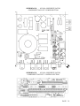
1
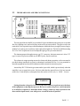
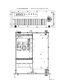
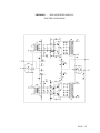
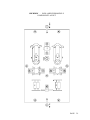
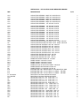
- NA 501 500W
FM POWER AMPLIFIER
USER AND MAINTENANCE MANUAL
PAGE 1
CONTENTS
1
GENERAL DESCRIPTION .................................................................................... 3
2
TECHNICAL FEATURES ..................................................................................... 4
2.1 FRONT PANEL COMMANDS AND SIGNALLING ............................... 4
2.2 THE REAR PANEL AND THE CONNECTIONS ...................................... 5
2.3 TECHNICAL SPECIFICATIONS ................................................................ 6
2.4 I/O REMOTE CONTROL SPECIFICATIONS .......................................... 6
3
INSTALLATION AND USE.................................................................................... 7
3.1 FOREWORD TO INSTALLATION ............................................................ 7
3.2 PLACING THE UNIT .................................................................................... 8
3.3 WIRING INTO THE MAINS ....................................................................... 9
3.4 ANTENNA CONNECTION .......................................................................... 9
3.5 LF CONNECTION ...................................................................................... 10
3.6 OTHER RECOMMENDATIONS ............................................................. 10
3.7 OPERATION ................................................................................................ 12
3.8 POSSIBLE MALFUNCTIONS ................................................................... 13
4
SERVICE AND MAINTENANCE ....................................................................... 14
5
Warranty.................................................................................................................. 14
6
SERVICE MANUAL.............................................................................................. 15
6.1 SYSTEM DESCRIPTION ........................................................................... 15
6.2 INTERNAL DESCRIPTION ...................................................................... 16
7
REPAIR AND REPLACEMENT OF DAMAGED MODULES ........................ 21
A.1
A.2
DRAWINGS
NA 501 amplifier front & top internal view (D1067) ............................................
NA 501 amplifier, rear and bottom internal view (D1068B) .................................
NA 501, general electric diagram, ver. 220-240Vac (E0893)
NA 501, wiring diagram (E0895)
NA 501, power supply front-end (E1003) ...........................................................
SRFB1K0AL2, RF control display, RF controls & measures board andcomponent
layout (E0894) ...................................................................................................
SRFB1K5ALM, 48V/40A SMPS regulator module diagram and layout power and
control section .....................................................................................................
NA 501, 500W RF amplifier assembly electric diagram (E0857) ..........................
SRFB1K0IN, 2-port RF input splitter diagram and layout (E0858) ......................
SRFB1K0PB, 2-port RF output combiner & LPF diagram and layout (E0859)
SRFB500W, 500W amplifier module diagram and layout (E0764) .......................
SRFB500W, 500W amplifier module - component layout ....................................
PAGE 2
NA 501
500W
1
FM POWER AMPLIFIER
GENERAL DESCRIPTION
The NA 501 is a highly integrated broadband solid-state Mos-Fet FM amplifier of 500W rated
power, fitted in a 4 unit 19" rack, which do not require any specific calibration to operate in the 87.5 ÷
108 MHz frequency range.
Its compact size, high efficiency, wide mains range acceptance, low maintenance requirements
and broadband construction, make this amplifier ideal in medium power repeaters, in unattended
posts, in N+1 systems and as a reserve.
Its sturdy, modular mechanical and electrical construction guarantees a high MTBF and an
easy maintenance. The modules are easily identifiable and inspectable with few interconnections
each with the other, through multi-pole connectors.
The nominal RF output power is obtained over the full FM range with a mere 8W drive and is
particularly stable against time, temperature and frequency variations being ALC regulated, with a front
panel adjustment. The output power may be varied from a minimum level to the nominal level and the
frequency varied over the full FM range, without retouching the drive power or any other adjustment
than the ALC control.
The output stage has a reverse intermodulation figure, which is lower than standard bipolar
construction, due to the all Mos-Fet design and approaches that of tube equipment.
A simple metering and alarm section completes the amplifier, permitting an easy check of
the functioning with few, unambiguous readings. Power readings and control are externally
available on a remote I/O port, for an external controller. A suitable one may be supplied on
request to permit full remote control of the Unit from the studio or another service centre.
The whole assembly is designed in accordance with the CCIR, FCC and tighter international
norms and conforms to the recent, strict
requirements for EMI susceptance and emission.
This equipment complies in particular to ETSI EN300.384 and EN 300.447
Broadcast and EMI/EMC standards, EN60065 and EN60215 safety
standards and FCC parts 73 & 74.
PAGE 3
2
2.1
TECHNICAL FEATURES
FRONT PANEL COMMANDS AND SIGNALLING
The front control panel carries the power on switch, the control meter, some alarm warning
led's and a RF monitor connector. On the bottom side, a gridding on the panel permits the output
of the ventilation air.
At the RF monitor output, BNC type, a sample of the output power is available which is
attenuated 54 dB typically (i.e. +6 dBm @ 500W output). Even if this output is fairly flat vs. frequency,
it is not suggested to use this for accurate harmonica analysis.
The switchable meter permits the reading of the most important operating parameters, i.e.
the forward and reflected power (500W f.s.) and the regulated and unregulated power supply voltage
(300Vdc f.s.).
The 2 led's light only in case of failure. The meaning of these led is summarised on the
following table:
LED
MEANING
VSWR
High RF output reflected power (> 50-60 W)
TEMPERATURE
High internal temperature, probably due to high environment temperature
or failure of the ventilation system.
Table 1:
warning led meaning
PAGE 4
2.2
THE REAR PANEL AND THE CONNECTIONS
REMOTE CONTROL
0678
MADE IN ITALY
AUX-1A Max
RF OUT
RF IN
115/230V ac-50/60Hz
1400/2400 VA
The rear panel allocates the RF power and the I/O ports in addition to the mains power cord and
fuse, the earthling screw and an auxiliary mains socket on some models. The power cord is not
removable. If it is required a longer cable than that provided in the factory (roughly 2 meters long), a
suitable 3x 1.5 mm sq. power cord may easily replace the original one. The fuse has a different rating
for 115 or 230Vac operation: be sure to adopt the right type for your mains network
The Antenna output is brought out on a type "N" connector, the input connector is also a "N"
type. A remote I/O port is available on a SUBD 25 poles, female connector.
The exhaust air output opening must not be obstructed during operation: wide room must be
provided during installation to permit a substained ventilation air flux. It is not permitted to
insert the equipment in a closed rack without a suitable external air extraction system.
An auxiliary IEC-320 female type mains outlet is provided, which is powered only when the
amplifier is on, to supply the exciter. No fuses other than the general fuses (16A) are inserted
on this line. Limit the power absorption from this outlet to low levels, i.e. 100W / 1A max.
,
WARNING !
Setting the mains voltage for 115 or 230V operation requires to gain access to the inner
of the equipment, removing the top cover. Be sure to remove the power cord from mains
to avoid direct exposure to hazardous mains voltage, which are always present on the
fuses and the input board, even with power on switch in the off position.
PAGE 5
2.3
TECHNICAL SPECIFICATIONS
@ 1kW RF output if not otherwise specified
- Frequency range:
- RF input power
- RF output power
87.5 ÷ 108 MHz
8W nom., 10 W max
500 W ±0.5 dB
-
50 Ω
N
N
BNC
RF input/output impedance:
RF input connector:
RF output connector:
RF monitor connector:
- Harmonic and spurious emissions:
- RF monitor attenuation:
< -70 dBc
54 dB, typ.
- Max total current handling capability on
the auxiliary socket:
1A @ 230 Vac, 100Wmax, not fused
- Mains supply requirements:
115 / 230 Vac 50/60 Hz <950W (1250 VA)
- Operating temperature range:
0 ÷ +35 °C recommended, -10 ÷ +50 °C max
- Dimensions, not including the handles:
483 x 177 x 535 mm (W x H x L)
See drawings
approx. 66Lbs (30 kg).
- Weight:
2.4
I/O REMOTE CONTROL SPECIFICATIONS
A remote I/O DB25 female connector, located on the rear panel, makes available 3 analog lines
to permit remote control and surveillance of the equipment as detailed:
Pin
1,3,21
9
10
13
Line
ground
Reflected Power
Forward Power
Power control
Range/use
common
0÷5V vs. 0÷550Wout Zo=10kΩ
(4 V typ. @ 500W)
0÷5V vs. 0÷550Wout Zo=10kΩ
(4 V typ. @ 500W)
External RF output control. 0-5V to full scale, low impedance
The remote I/O signal and control
DB25 female connector, on the rear
panel
PAGE 6
3
3.1
INSTALLATION AND USE
FOREWORD TO INSTALLATION
Although in most cases no special instruments are required, have skilled personnel install the Unit.
To make best use of the Unit’s capabilities and prevent damage to the unit, comply with the
recommendations throughout this manual.
When in doubt, or if any technical problems should arise during the installation procedure, Nicom
strongly recommend the Unit not to be tampered with in any way by unskilled personnel and will be
glad to supply qualified after-sale service.
As a rule, the user should not have access to the inside of the Unit for normal installation and use.
Tampering with the factory settings makes the warranty void and might also affect Unit’ performance,
causing costly damage.
,
WARNING !
NO ADJUSTMENT OR INTERNAL PRESETTING IS REQUIRED FOR NORMAL
OPERATIONS. THE UNIT SHALL BE PROPERLY GROUNDED AND BE OPERATED
WITH ALL THE COVERS CLOSED TO PREVENT ELECTRICAL HAZARDS IN
OPERATION AND FULLY COMPLY WITH CE EMI AND SAFETY REQUIREMENTS.
NEVER TOUCH THE INSIDE OF THE UNIT WITHOUT FIRST DISCONNECTING IT
FROM THE MAINS. DANGEROUS AC, DC AND RADIO-FREQUENCY VOLTAGES ARE
PRESENT INSIDE AND BECOME ACCESSIBLE WHEN THE COVERS ARE REMOVED.
——— MAINS VOLTAGE MAY KILL ———
PAGE 7
3.2
PLACING THE UNIT
Install Unit in a dry, sheltered but well-ventilated room away from dust, moisture, insects and vermin
(mice).
Place Unit as close as possible to the antenna to prevent excessive power loss in the cables. If this
is not feasible, use antenna cables of suitable cross-section.
Room size shall be such that the Unit can be placed in an upright position and that technical personnel
can easily carry out routine or extraordinary maintenance. The minimum recommended size is 2.5m
x 2m, and 2.2m high when there is no other broadcasting or support equipment nearby.
The room must be ventilated to ensure that the inside temperature never exceeds 35°C. Even if
45°C is the max. allowed temperature: it is anyway suggested not to approach to this limit.
This condition cannot generally be met when the exhaust cooling air is not pushed outside and is
fed back into the room. This is even truer if more than one Unit is installed in the same location. An
efficient ventilation system is thus required in the room. Air exchange in the room shall have a minimum
flow-rate of 500 metres cubed per hour or more.
If the Unit is fitted in a rack system, the back door of the rack cannot usually be fixed in place. If
a completely closed assembly is needed, a suitable ventilation extraction unit must equip the system.
To aid air ducting, an optional flange may be retrofitted on the ventilation outlet to which a duct can
be attached to convey hot air outside. In this case remember that the NA 501 internal fans are lowpressure units: some sort of external air extraction blower is than imperative on the exhaust air duct.
Vents in the walls and any other openings shall be fitted with a metal grating to keep rodents out,
and with a dust filter. Make absolutely certain that no water can seep through the vents or the air
exhaust duct or antenna-cable grommet, and that the floor cannot be flooded during heavy rainfall. If
not impedited by proper air filtering, insects in some location may be conveyed in the internal heatsink,
accumulating on it and finally obstructing it, causing overtemperature alarm.
Even moisture and/or dust, when contained in the air or in the room in excessive quantity, may cause
condensation build-up in the amplifier. When the system is periodically switched on and off, this can
trigger destructive electric arcs and short circuits and thus cause damage that is not covered by the
guarantee.
PAGE 8
3.3
WIRING INTO THE MAINS
The NA 501 is powered by a single-phase line. Mains capacity must be at least 2kVA and the
nominal voltage is 230Vac. In some countries, where 115Vac is the norm, this voltage must be
internally set in the factory or by skilled people before installation.
While the power supply regulator accepts a wide input voltage (190 ÷ 250 Vac), operation near
the lower input voltage on high impedance lines must be avoided: if the line drops more than 10 volt
at full load, the low line sense circuitry may trigger an oscillating turn-on / turn-off cycle, which is very
dangerous. In this cases adopt an external line stabiliser.
The nominal mains input range (190 ÷ 250 Vac) is achieved when the primary side of the main
transformer is wired to the 230 V tap. Two other taps, the first one slightly lower (220 V), the second
higher (240 V), are available to adjust the input voltage range of ±10 V. In countries were a stable
240V is the norm, it is important to set this tap on the transformer. In this case the allowed voltage
range window must be shifted higher to avoid nuisance trip at occasional higher mains voltage. See
proper section in the service section of this manual.
To ensure proper operation and comply with the safety regulations, efficient earthling is required.
Use the yellow/green lead in the power cable. The cable’s neutral lead is blue. Never connect the earth
to the mains’ neutral lead.
The cable connecting the NA 501 mains input terminal block to the external board should consist
of leads of adequate cross-section. Recommended values are 1.5 to 2.5 mm squared.
Do never switch the Unit on without antenna connection, even when no RF drive is on.
3.4
ANTENNA CONNECTION
An "N" output connector is fitted at the back of the amplifier module. It is very important to check
that the antenna, the connecting cables and the connectors are suitable for 500W.
The antenna coupler too, should be capable of adequate power; its input connector shall be "N"
PAGE 9
3.5
LF CONNECTION
To maximally avoid earth loops, wire the modulation signal line directly on the exciter, with high
quality shielded and preferably balanced cable. Ground the shield only on the exciter LF input
3.6
OTHER RECOMMENDATIONS
The ambient temperature shall range between -5°C and +30°C (35°C max. peak). It is advisable
to hang a min.-max thermometer on the wall to display any variation.
Air conditioning at 20 ÷ 25°C would obviously be the best solution, but installation and operating
costs are generally excessive. Thermal isolation and efficient ventilation with a thermostat-controlled
blower are generally the most advantageous solution.
Mains fluctuation and electric discharges due to the weather or nearby industrial machinery may
cause significant trouble, especially in mountain areas and in places close to industrial areas. In such
cases, it is advisable if not indispensable, to install a protector, and insulating transformer or possibly
an electromechanical mains voltage regulator. NICOM can provide all these accessories on request.
Since the total cost of the plant, inclusive of broadcasting equipment, antenna system and
installation, is rather high, a certain percentage of the budget should be estimated for buying and
installing suitable protection and conditioning facilities as described above.
Depending on location, the share of total cost should be around 20 ÷ 30%; with this expenditure,
however, the machinery will operate under optimum conditions, its useful lifespan will increase and,
above all, the incidence of accidental breakdowns due to ambient or mains trouble will be reduced.
PAGE 10
,
!! WARNING !!
OPERATION WITHOUT THE ANTENNA OR WITH A FAULTY ANTENNA
CONNECTION MAY CAUSE DEGRADATION AND POSSIBLE DESTRUCTION
OF THE FINAL STAGE. THIS FAILURE IS NOT COVERED BY THE WARRANTY.
AVOID TO USE TOO POWERFUL EXCITERS. AN INPUT POWER HIGHER THAN
12W MAY PERMANENTLY DAMAGE THE RF TRANSISTOR CAUSING A COSTLY
DAMAGE, WHICH IS NOT COVERED BY THE WARRANTY. A STABLE AND PROPERLY
REGULATED 20÷25W EXCITER, LIKE NICOM'S NT20 or NT30 ARE THE BEST CHOICE.
NA 501 driven by a typical NICOM exciter generates a very clean RF output. Neverthless if any
strong RF signal, coming from nerby transmitters is coupled to the antenna, it may cause intermodulation
in the output transistors and generate spurias. In this case a tuned output filter may be required to
remove the problem.
It is mandatory to provide adequate ventilation to the Unit to maintain its internal temperature as
low as possible, in the recommended range 5 ÷ 25°C. Even if the Unit may sustain 45°C, and
occasionally slightly higher temperatures, his life expectancy will be impaired by high temperature.
As general rule the life expectancy may be halved by each 10°C increase in ambient
temperature, over 30°C.
PAGE 11
3.7
OPERATION
Check that the antenna, the subsequent power amplifier or a suitable dummy load is connected to
the amplifier RF output. If the NA 501 drives a tuned tube amplifier, check that the input of the power
amplifier is already tuned on the wanted frequency. Control that the power cords are correctly
connected to the amplifier and its driver and both the Unit are off. Before connecting to the amplifier,
control that the exciter power is set at zero or a very low level (<1W) and the frequency is correctly
set. Check that the exciter output signal is fed to amplifier input, then:
1) Switch-on the power-on switch on the NA 501:
- the switch will glow red.
- Internal blowers will start.
- No led should light on.
- No RF output power should be present.
2) Properly position the meter switch to observe the RF output increasing on the amplifier.
3) Switch-on the power-on switch on the exciter
4) Slowly raise the drive power to the required level, i.e. 8 ÷ 10W.
- The RF output power should rise from zero to the nominal 500 Watt, if the output power
adjustment is set is to maximum on the amplifier front panel.
- No led should light on.
- As a general rule, the input power must be 20% higher than the minimum level required to the
full output power (i.e. 8W if 10W are enough to obtain 500W on the output).
5) Control and note for future reference the correct reading of the operating parameters through the
internal instrumentation, which must indicate the following values:
-
FORWARD POWER:
REFLECTED POWER:
REGULATED VOLTAGE:
UNREGULATED VOLTAGE:
up to 500W
< 50 W, typ. 0 ÷ 20W
48V (300V meter range)
140V ±15%
Some amplifiers do not permit to read the regulated and unregulated voltage on the internal meter.
The installation of the amplifier is thereby completed. A spectrum analysis is now advisable to
assure no spurious products due to internal or external causes (i.e. reverse intermodulation on the final
stage) are generated. Nicom wishes you success in your work and remind you that they are always
available for further information or to tackle any specific problem.
PAGE 12
3.8
POSSIBLE MALFUNCIONS
No led alarm must be on during regular functioning: following is a list of possible malfunctions causes.
"VSWR" led on
This led turns on when the reflected output power exceeds the 40-50 W threshold. In this case, do
not operate the system and check antenna, relevant wiring and connectors.
When the Unit is connected to a successive amplifier, re-tune the latter's input to obtain the smallest
reflected power.
This light should never turn on; it might however flash briefly at low power when firstly tuning the
input of an NA 501-driven tube amplifier or a cavity band-pass filter.
"Temperature" led on
This led turns on when the internal temperature is excessive. Reduce environment temperature and
increase room ventilation. In this case, it is important that the hot air released by the Unit be exhausted.
Control regular functioning of the internal ventilation fans and clean any externally applied dust filter,
if any.
PAGE 13
4
SERVICE AND MAINTENANCE
Since the NA 501 is cooled by air, it is subject to clogging by dust. Because of the high-quality
materials used in their manufacture, if it is installed as set forth under “INSTALLATION AND USE,”
it will not require special maintenance for quite some time.
A regular service routine, mainly to remove internal dust is suggested over a 6 month to a year rate.
Take present that 90% of the air circulation is restricted to the main internal ventilation channel and
do not affect the components. Regularly change the ventilation fan, especially in higher temperature
environments. A 2-year rate may be prudential: always use the same high quality, ball bearing fan type.
After a few years of continuous service, it is recommended that the Unit be overhauled in the
factory or in a specialised laboratory, where the characteristics can be checked against the initial ones
and recalibration can be made when needed.
It is also especially important that the power supply be over-hauled when the Unit has been working
at high temperatures, over 30 ÷ 35°C.
Never change or cause the original settings to be changed when the necessary, complex testing
equipment and standard calibration procedure are not available.
5
WARRANTY
Like all NICOM's solid state equipment, the NA 501 carries a 2-year Warranty on all its
components with the exclusion of the final RF power module, which may be damaged by faulty output
connections.
This warranty is null and void if the Unit is tampered with or if failure is due to improper use, wrong
installation or external causes, such as mains overvoltage.
This warranty covers work done exclusively in our laboratories and in those of our agreed
representatives.
The goods shall be delivered carriage prepaid to the laboratory and shall be returned freight
forward.
This warranty does not cover any consequential damage due to non-operation or faulty operation.
PAGE 14
6
6.1
SERVICE MANUAL
SYSTEM DESCRIPTION
3 basic sections compose the NA 501: the RF amplifier box, the power supply and the control
and metering section.
The RF section comprises 1x 500W amplifier modules connected through strip-line combiners. All
the RF transistors are Mos-Fet type. A low-pass filter with directional coupler completes the section,
which is completely screened by a metal box, to comply with EMI requirements. A fully planar design
permits an immediate access and inspection to the 2 internal modules.
The power supply comprises a mains transformer, whose output is rectified and filtered and a
highly efficient Switch-Mode Power Supply regulator.
The RF control section is built on one small board. It performs RF AGC and protection control;
providing metering and an interface to the external I/O port. Both direct and reflected power are
displayed and provided as proportional analog signal at the Remote I/O port. Through this port is
possible as well to command the RF output power, overcoming the internal front panel regulation.
6.2
INTERNAL DESCRIPTION
NA 501: Block diagram
PAGE 15
The NA 501 amplifier comprises 6 internal different modules/boards plus some spare
components, as can be seen in the drawing of the inner contents and in the "General wiring diagram";
both comprised in this manual:
-The power supply transformer, rectifier and capacitor
-The Switch Mode Power Supply regulator
-The RF control and measure board
-The input RF power splitter
-The 500W RF power amplifier module
-The output RF combiner, Low-Pass Filter and coupler
For the detailed description of each module on the following pages, always refer to the
corresponding electrical diagram, in the relevant section of the manual.
,
WARNING !
THIS SECTION IS ONLY AIMED TO GENERAL KNOWLEDGE OF THE UNIT AND
FOR SERVICE PURPOSE BY SKILLED PERSONNEL. AS EXPLAINED IN THE
PREVIOUS SECTIONS, INTERNAL ADJUSTMENTS ARE NOT REQUIRED DURING
NORMAL OPERATION. TAMPERING WITH INTERNAL SETTINGS VOIDS THE
WARRANTY, MAY HARM THE UNIT AND JEOPARDIZE THE GUARANTEED
PERFORMANCE.
IN ADDITION, MANY MODULES ARE TOO MUCH SPECIALIZED AND
DIFFICULT TO REPAIR EVEN BY SKILLED TECHNICIANS AND MUST BE
REPLACED IN CASE OF NEED BY BRAND NEW ONES AND POSSIBLY RETURNED
BACK TO FACTORY TO VERIFY IF THEY CAN BE REPAIRED.
ANY ISPECTION ON THE MODULES DESCRIBED ABOVE MUST BE EXECUTED
WITH THE TOP COVER REMOVED AND OFTEN WITH THE OPERATING UNIT
CONNECTED TO THE MAINS. ALTHOUGH MOSTLY OF THE PARTS UNDER
VOLTAGE ARE INSULATED AND ARE NOT EASILY ACCESSIBLE, THIS EXPOSES
TO THE RISK OF ACCIDENTAL CONTACT WITH THE MAINS VOLTAGE. TO AVOID
IT, ALWAYS USE INSULATED TOOLS AND NEVER TOUCH THE SUPPLY
TRANSFORMER, THE MAINS SWITCH OR THE MAINS SOCKET WITH MAINS
CONNECTED. NEVER OPERATE THE EQUIPMENT WITH THE COVERS REMOVED.
REMOVAL OF THE BOTTOM RF COVER MAY LEAD TO IMPROPER FUNCTIONING
OF ANY ELECTRONIC MEASURING METER DUE TO HIGH RF FIELD.
--- MAINS VOLTAGE MAY KILL! ---
PAGE 16
6.3
The power supply components
The power supply components, other than the boards below described, are very few: mainly
the power transformer with a power relay, a bridge rectifier and a power capacitor, which delivers
the raw rectified dc power to the SMPS regulator module.
The unregulated dc voltage, nominally 140 Vdc, may range 120 ÷ 170 V. The primary tap on
the power transformer is factory set on the 230V input, allowing a mains range approximately
200 ÷ 250 Vac. Should the mains voltage be 240Vac nominally, it is suggested to change the
transformer tap to that voltage. If the mains voltage is a stable 215 ÷ 225 Vac, the transformer
tap may be left as factory set. Only if there are frequent occasional drops of mains input below
195V and consequent system stops, it is suggested to lower the input tap to 220V.
To do that, the power cord must be disconnected from the mains, the top cover must be
removed and the transformer voltage terminals may be accessed.
An USA version is provided with a someway different transformer and general wiring (see the
appropriate electrical diagram and internal layout). In this version, some jumpers must be preset
on the equipment's internal terminal board TB1 to provide 115 or 230Vac operation, if not factory
wired. In details these settings are:
220 Vac
115 Vac
6.4
1/P3 to 3/P4
3/P3 to 3/P4 and 1/P3 to 1/P4
The Switch Mode Power Supply regulator
This module performs an efficient regulation of the raw dc input, nominally 140V ±15% to a
lower 48V ±1%. Being its efficiency very high, very little heat is produced in the regulation process.
The nominal current capability of the regulator is much higher than requested, and approaches
40A @ 48V.
A control I/O connector on an upper daughter board permits a remote control of the regulator
NA 501:
Positioning of the power supply
internal terminal board
12 3
12 3
P4
P3
PAGE 17
by the Unit controller, i.e. output on/stand-by, current and voltage monitoring, status prompting
and alert.
A fast 80A semiconductor-grade protection fuse is screwed on the board: it may be fused by
the crowbar protection in case of switching transistor damage. If this happens a first attempt to
replace the fuse may be accomplished, after having verified the integrity of the power transistors.
Usually something is broken so causing the fuse blow-up.
Reparation of this module in the field is very difficult if any component other than the fuse and/
or a power transistor failed. It is suggested to substitute the module with a new one and send
back the damaged unit to the factory for inspection and possible reparation.
6.5
The RF control and measure board
This small board carries all the circuitry to control and protect the RF amplifier stage. Let us
consider its various loops.
Two identical buffers, IC4a and IC3a, insulate and amplify the direct and reflected signal detected
on the RF output coupler, with different gain. The main direct power regulator loop is built around
the subsequent IC4d op-amp, which compares the sensed signal with the preset power level on
RT5. Adjusting this trimmer, the RF output power may be varied to values different from that
factory preset. Never exceed a safe 500W on RF output, even if the amplifier is usually able to
easily threpass this limit, to have some safety margin. The output of IC4d constitues the AGC line,
which is buffered by IC5 to drive the RF transistor gates. Both the two sections of IC5 are in
parallel to increase the current capability of the external AGC line.
The reflected power protection is managed by IC3c, which compares the reflected sensed signal
to a fixed threshold, which is set to 40/50W, as determined by R35 and R36. The output of IC3
adds on the internal AGC line though D14. The action of this circuit is proportional: i.e. the output
power is continuously decreased till the fraction which is reflected back no more exceeds the safe
maximum level. There is no RF complete switch off even with severe load mismatch.
Both direct and reflected signal lines are conveyed to the remote connector through insulating
10kohm resistors
The temperature protection on the output stage is performed by IC4b, which trips when the
temperature sense line crosses its preset threshold, completely disabling the RF output. The temperature sensor is mounted on the heatsink, near the RF transistors, and is constitued by a precise
PTC resistors, which varies its resistance accordingly to the temperature.
PAGE 18
On this board a small negative rectifier and a regulator (TR5) provides the negative bias to
completely disable the RF power, if needed. The positive regulator TR4 derives the positive 11.3V
board supply from the +48V regulated line.
6.6
The input RF power splitter
The purpose of this simple board is mainly to divide the input RF drive power in two identical
signals, one for each power amplifier module, providing a good insulation between each output
port (>20 dB, typ. 23 dB minimum on the whole FM band).
This is done by a Wilkinson type printed coupler, followed by the balancing resistor array
R21 ÷ R24.
A directional coupler senses the input RF level and RT1 is regulated to provide the overdrive
protection circuit trip at the right maximum input level. The board supports also the direct (or
forward) and reflected detector sensitivity trimmers, whose input comes from the output board.
Two additional lines support the RF module bias (or AGC) line and the temperature sensing
PTC thermistor.
6.7
The RF power amplifier module
This module is built around a couple of "Gemini type" Mos-fet transistors each one forming a
300W push-pull amplifier.
Discrete Wilkinson-type couplers equip both the input and the output module section, doing
the job of dividing and recombining the input and output signals, providing a suitable insulation
between the transistors.
A small balancing resistor R1 is mounted on the input splitter, while a much bigger resistor
R14 is mounted in the output combiner.
A group of C, R and L RF decoupler and dampening components are mounted on the positive supply line of each amplifier, plus a small value resistor, R12 and R13, for possible separate
current detection of each supply leg.
The gate bias is separately adjusted through R15 and R16 on each section. Do not tamper
the factory bias preset values!
The full power output of the whole module exceeds 600W, to provide some room for coupling
losses on the combining stages of higher power amplifiers, like the same NA 501.
PAGE 19
6.8
The output RF power combiner, LPF and coupler
This module is symmetric to the input power splitter and is another printed Wilkinson coupler,
whose power management capability is obviously much higher than the input board. In this
case the power balancing resistors are high power devices, whose centre connection is referred
to ground through an inductor, which discharges any static electricity on the antenna up to a
relevant amount of power.
The power combiner is followed by a printed low-pass filter, which attenuates the harmonic
products generated by the amplifiers.
3 directional sample lines derive two rectified voltages proportional to the direct and reflected
output power and a RF signal for external monitoring purposes.
PAGE 20
7
REPAIR AND REPLACEMENT OF DAMAGED MODULES
The NA 501 is a high reliability Unit, as much effort was done in the design and development
stage to assure the maximum reasonable working margin for each part. Nevertheless, as all Unit
which works 24 hours a day for years, some failures are possible, especially in those environments
which over-stress the Unit, like hot or dusty or moist places, or subjected to wide mains fluctuations
or static discharges and things like that.
In the event of any failure an appropriate analysis must be done to avoid subsequent failures
due to faulty ambient conditions. A often underestimate cause of failure is simply a too high ambient
temperature or insufficient ventilation. Improving the ambient and system ventilation as suggested
in the installation paragraph of this manual, usually fix the problem.
Other obvious causes may be dust clogging and ventilator fan failure. A regular service and
maintenance routine will avoid these sources of problems and it is suggested to change the ventilator
each two years, even if no damage is still visible, especially at high ambient temperature.
No air pipe must be attached to the ventilator fan output for air ducting, if an external extacting
fan is not installed in that system.
In any case, if the amplifier fails, some work must be done on the Unit to fix the problem. With
the appropriate spare parts, most of repairing work may be done on site, without need of special
tools and often without need of any solder joint.
Not much needs to be said about the general boards and components changing: virtually all of
them may be changed in few minutes, without retouching the adjustments. Most of them are
immediately accessible or needs a minimum of dislocation of other components and plates. Only
the RF boards need a deeper look.
RF boards are delicate modules, which contains some parts as flanged power transistors and
resistors which must separately be screwed on the supporting heatsink and may be easily damaged
by improper handling. These boards are the 500 W power amplifier modules and the RF output
combiner.
Repairs of these modules are usually made in the factory or in a specialised laboratory, if possible
at all. If the p.c. board is damaged perhaps only the costly RF active devices may be recovered.
Nevertheless, very often this is worthless because, in case of major damages, these parts are
internally electrically damaged or degraded.
Repair of the RF modules requires too, at the end of the reparation, a full check of the module's
working parameters in a dummy fixture or in a test assembly which are not available even in most
specialised laboratories. For these reasons repairs of the modules, specially the higher power
amplifiers, is discouraged at the most and the broken one must be replaced by new parts with the
PAGE 21
same identical characteristics, fully tested at the factory.
To replace the modules avoiding as much as possible to damage the new part or the old
transistors, if not already broken, carefully follow the subsequent steps:
1) Remove the amplifier cabinet from the rack, after having disconnected from its rear
connectors the RF input and output cables, the power supply and the control cables.
Disconnect also the ground cable from its screw.
2) To investigate on the damaged parts or to test the reparation, it may be required to externally
connect the removed cables and the RF output load to the amplifier assembly in manner
to permit inner inspection of the top and bottom of the Unit. If the latter is placed on a
small stand aside of the main rack, the internal cables are usually long enough to permit the
connections, avoiding extension cables.
3) Open the bottom cover of the cabinet and remove the screen from the damaged module(s),
if any.
4) If the damage is not immediately visible, it may be helpful to measure the currents sunk by
each 300W sub-module amplifier. To this aim a low ohmic value shunt resistor is inserted
in series to the 48V power supply of the module's subsections (R12 and R13, 10mΩ).
To measure the current sunk, the amplifier assembly must be completely connected and
powered with and without RF. A sensitive, RF proof, digital voltmeter must be used to
measure the voltage across the shunt resistors, which vary from nearly 1 mV at no load to
100 mV at full power.
Take care: most of low quality digital or analog meters are not able to do this reading,
because they are affected by the high RF field and their reading is completely meaningless!
WARNING: great care must be paid not to accidentally short-circuit the resistor leads to
the ground with the voltmeter probe tips, during the measurements!
5) When properly functioning at full power, each module 300W subsection will sink 8 ÷ 10
Amperes, i.e. 80 ÷ 100 mV across the shunt resistor. The absorption must be balanced
±10% around the mean value on each amplifier. A lower or higher value may mean a
module failure.
6) Remove the power supply cable screwed on a centre terminal in the board and the small
bias cable.
7) Unscrew the input and output RF connections, at the module opposite sides.
8) Carefully unscrew the RF transistor flanges from the heatsink base-plate. This operation,
if not properly done, may mechanically over-stress the transistor, cracking the internal delicate beryllium-oxide ceramic which supports the active silicon dies and determine
unrecoverable
PAGE 22
damage of the device.
CAUTION: beryllium-oxide is toxic and must not be thrown with domestic refuse but in
specialised toxic material disposals. No special handling precaution must be paid when the
transistors or power resistors are not mechanically broken, apart those deriving from the handling
of mechanically fragile (and very costly) devices. If the transistor or resistor flange is broken,
avoid to get in touch with it and the brittle white exposed internal ceramic or inhaling dust of it.
Dispose the transistor or the entire broken module as previously described.
9) Make a note of the position and the length and remove the threaded screen spacers and the
board fixing screws.
10) Remove the broken module and clean the supporting heatsink base-plate before mounting the
new one.
11) Smear thin heat-conductive silicon grease below the flanges of the power transistors and resistors
of the new module, before mounting it.
12) Position the new module, placing the threaded spacers and screws over the p.c. board avoiding
to tighten them. When all the screws are placed, control the correct alignment of the transistors
and resistors fixing holes and tighten the screws and spacers.
13) Insert the proper screws and washers, if any, across the transistors and resistors and carefully
tighten them in several, alternate steps.
14) Reconnect the power supply and bias cables to the module.
15) Turn-on the whole amplifier fully connected to the supporting power and control rack without
RF power, with RF load connected and driver exciter off. Enable the equipment, with the exciter
still off.
16) Measure the bias current of the two transistors on the module, as explained on previous
paragraphs 4 and 5. They were factory adjusted to 100 mA (1mV).
17) If the currents are off the range 50 ÷ 200 mA (0.5 ÷ 2 mV), carefully retouch the bias trimmers
on the board. A small clockwise rotation increases the bias current.
18) Reduce the output set power to a low value, acting on the front panel power set trimmer and
turn on the exciter power.
19) Slowly increase the power-set and measure the balance of the current drained by each module
at half level and at full power. Verify the limits written in paragraph 5.
PAGE 23
20) Turn off the equipment, reassemble the screening covers and the bottom panel of the Unit
and reposition it in its working location with full connections.
21) Perform a limited period of test at full power, i.e. 500 ÷ 550 W and then reduce power at
maximum nominal working level, i.e. no more than 500 W.
PAGE 24
NA 501 AMPLIFIER - FRONT & TOP INTERNAL VIEW
PAGE 25
NA 501 AMPLIFIER - REAR & BOTTOM INTERNAL VIEW
REMOTE CONTROL
0678
MADE IN ITALY
AUX-1A Max
RF OUT
RF IN
115/230V ac-50/60Hz
1400/2400 VA
PAGE 26
14
13
12
11
10
9
8
7
6
5
4
3
2
1
10
9
8
7
6
5
4
3
2
1
+VS
C5
0u1
C4
0u1
R4
470
CON10FLATM
CM3
CON14FLATM
CM2
CON26FLATM
+VS
1
R6
47K
3
R5
47K
VREF
TL431
IC1
PW_INGRESSO
+VS
1K
R3
JP1
MON_ING
0A1
+VS
3
+VS
REFL. OUT
220
R35
100K
1K
R39
R22
100K
1K
R24
TEMP SENSE
C18
100p
10K
R34
C19
100p
C22
0u1
C13
100p
1K
R38
C14
100p
1K
R21
1K
R23
10K
C15
0u1
22K
R11
R45
4K7
R47
C7
0u1
R12
10K
VERT.
VREF
REG.
R49
47K
R48
10K
C6
0u1
REG. Vu
C8
0u1
VREF
1
R19
+
-
+
3
+
R36
3K32
-
9
10
R37
R20
412
-
2
IC4A
1
C21
0u1
IC4C
TLC274
3K32
8
TLC274
475K
R10
IC2B
TLC274
7
D3
4148
C9
0u1
3K32 +VS
R9
2K8
5
6
R8
10K
R46
3 5K
VREF
9
10K
681
4148
C23
0u1
PW_DIRETTA
1K
R41
R40
10K
R27
1K5
R13
C20
100n
PW_RIFLESSA
R26
C16
0u1
R83
R
8
1
IC2A
TLC274
+VS
D7
1M
R42
4148
D5
1M
R25
+
3
TLC274
10
VREF
4148
-
2
IC2C
R17
90K
R14
22K
D2
R16
30K
R15
90K
+VS
4
11
R7
1
2
C26
2u2
12
13
1K5
R43
R29
47K5
5
6
+
-
3K32
R30
R28
22K1
VREF
TEMP
D1
+
-
7
4n7
14
100p
IC4D
TLC274
C24
C25
TLC274
IC4B
2n2
C17
CI RISERVIAMO A
TERMINI DI LEGGE
LA PROPRIETA' DI
QUESTO DISEGNO,
CON IL DIVIETO
DI RIPRODURLO O DI RENDERLO NOTO A DITTE CONCORRENTI O A TERZI
4K75
R44
4148
D8
C11
10u
+
12
+
-
4K75
R50
1
C27
100n
NE5532
IC5A
+VS
C28
100n
5
6
7
8
14
TLC274
IC2D
-VSOUT
6
7
+VSIN
+
6
5
100
R51
1K5
R33
NE5532
Date:
Size
A3
Title
7
ROS
D6
IC5B
1
10u
C12
-VS
C10
10p
2
Tuesday, March 25, 2003
E0977 - File E0977.sch
Document Number
Sheet
1
RFB1001SM - SCHEDA CONTROLLO (ANALOG)
SISTEMI ELETTRONICI SIEL - MILANO - ITALY
R53
110K
-VS
3
2
R52
6K19
R32
100K
-
13
R31
22K1
ICL7662
CAP
GND
CAP
1
IC3
+VS
4
3
2
1
1
2
F4
2
26
25
24
23
22
21
20
19
18
17
16
15
14
13
12
11
10
9
8
7
6
5
4
3
2
1
1
2
4
-
11
8
4
+
CM1
of
1
C29
1n
100
R54
D4
ON
R18
1K5
+VS
Rev
A
NA 501SM AMPLIFIER - ELECTRICAL DIAGRAM (220-240Vac)
CONTROLS & MEASURES BOARD
PAGE 27
NA 501 - WIRING DIAGRAM
PAGE 28
P2
1
2
3
3
C1
1u 1
T1
2
4
C2
1u
C3
0u1
4
3
2
1
3
1
2
CI RISERVIAMO A
TERMINI DI LEGGE
LA PROPRIETA' DI
QUESTO DISEGNO,
CON IL DIVIETO
DI RIPRODURLO O DI RENDERLO NOTO A DITTE CONCORRENTI O A TERZI
P3
R2
3A
F3
R1
1
25A
25A
F1
F2
Date:
Size
A4
Title
1
2
3
4
P1
Saturday, February 22, 2003
E1003 - File E1003.sch
Document Number
Sheet
1
RFB1001SM - 115/230V POWER SUPPLY FRONT-END
SISTEMI ELETTRONICI SIEL - MILANO - ITALY
P4
3
C4
0u1
1
2
P6
2
P5
of
1
Rev
A
NA 501 AMPLIFIER - POWER SUPPLY FRONT-END
PAGE 29
PW_DIRETTA
PW_RIFLESSA
+
5
V+
+5V
R56
100K
-
6
R68
3K6
2
TLC272
7
1K
IC6B
1K
R55
C30
0u1
3
R67
1K2
SW1
1
2K
C35
470u
200u
L1
MC34063A
COMP
U4
ISWC
ISWE
TCAP
IPK
IDC
R75
10K
aDL5
R71
1K
DIRETTA
INGRESSO
RIFLESSA
dp
5
gDL5
R70
dDL5
R72
1K
1
2
3
7
8
5819
C34
470p
4052
Y0
Y1
Y2
Y3
INH
A
B
X0
X1
X2
X3
U2
R66
0.56
+VS
1
5
2
4
6
10
9
12
14
15
11
D12
+VS
R74
10K
R73
1K
Y
X
+VS
3
13
C33
100u
A
A
D11
10V
2
3
4
5
6
7
8
9
2
1
R57
DL1
R64
22K1
R63
221K
a
f
A
e
A
dp
NC
NC
VCC
VDD
R61
20K
GND
R59
220K
4148
VSS
D9
D10
R62
78K
R65
1K
4148
17 A
16
15 bcDL1
14
13 bcDL1
12 A
11
10
+VS
A
NC
b
g
c
A
d
dp(R)
VEE
+VS
aDL2
fDL2
A
eDL2
A
3
2
2
3
4
5
6
7
8
9
+
-
A
NC
b
g
c
A
d
dp(R)
1
C31
0u1
IC6A
TLC272
+VS
R60
33K
DISP7_1
C32 10n
a
f
A
e
A
dp
NC
NC
DL2
8
4
PW_INGRESSO
1K
17 A
16
15 bDL2
14 gDL2
13 cDL2
12 A
11 dDL2
10
3
+5V
1M2
TL431
1K5
R78
1K
IC7
a
f
A
e
A
dp
NC
NC
DL3
R82
2
3
4
5
6
7
8
9
R79
aDL3
fDL3
A
eDL3
A
1
2
R58
2
1
R77
1K
DISP7_1
C40
100p
C36
0u22
C38
0u1
aDL4
fDL4
A
eDL4
A
dp
2
3
4
5
6
7
8
9
A
NC
b
g
c
A
d
dp(R)
40
39
38
37
28
29
27
36
35
34
33
31
30
32
D13
5V1
V-
ICL7107
OSC1
OSC2
OSC3
TEST
BUFF
A/Z
INT
REF HI
REF LO
CREF+
CREF-
IN HI
IN LO
COMMON
U3
17 A
16
15 bDL4
14 gDL4
13 cDL4
12 A
11 dDL4
10
1K
R69
A1
B1
C1
D1
E1
F1
G1
A2
B2
C2
D2
E2
F2
G2
A3
B3
C3
D3
E3
F3
G3
AB4
POL
BP
aDL5 2
3
A
4
5
A
6
7
8
9
aDL2
bDL2
cDL2
dDL2
eDL2
fDL2
gDL2
aDL3
bDL3
cDL3
dDL3
eDL3
fDL3
gDL3
aDL4
bDL4
cDL4
dDL4
eDL4
fDL4
gDL4
12
11
10
9
14
13
25
5
4
3
2
8
6
7
-VS
bcDL1
23
16
24
15
18
17
22
DISP7_1
Date:
Size
A3
A
NC
b
g
c
A
d
dp(R)
19
20
21
a
f
A
e
A
dp
NC
NC
DL5
Tuesday, March 25, 2003
E0977 - File E0977.sch
Document Number
Sheet
1
RFB1001SM - SCHEDA CONTROLLO (DISPLAY)
SISTEMI ELETTRONICI SIEL - MILANO - ITALY
R80
100K
DISP7_1
Title
a
f
A
e
A
dp
NC
NC
DL4
CI RISERVIAMO A
TERMINI DI LEGGE
LA PROPRIETA' DI
QUESTO DISEGNO,
CON IL DIVIETO
DI RIPRODURLO O DI RENDERLO NOTO A DITTE CONCORRENTI O A TERZI
R76
470K
0u1
C39
C37
47n
17 A
16
15 bDL3
14 gDL3
13 cDL3
12 A
11 dDL3
10 dp
R81
220K
A
NC
b
g
c
A
d
dp(R)
1
2
MON_ING
of
A
17 A
16
15
14 gDL5
13
12 A
11 dDL5
10
1
Rev
A
+5V
SRFB1K0AL2 - RF CONTROL DISPLAY- ELECTRICAL DIAGRAM
PAGE 30
SRFB1K0AL2 - RF CONTROLS & MEASURES BOARD
COMPONENT LAYOUT
PAGE 31
SRFB1K5ALM - 48V/40A SMPS REGULATOR
ELECTRICAL DIAGRAM - POWER SECTION
PAGE 32
SRFB1K5ALM - 48V/40A SMPS REGULATOR
ELECTRICAL DIAGRAM - CONTROL SECTION
PAGE 33
SRFB1K5ALM - 48V/40A SMPS REGULATOR
COMPONENT LAYOUT - POWER SECTION
SRFB1K5ALM - 48V/40A SMPS REGULATOR
COMPONENT LAYOUT - CONTROL SECTION
PAGE 34
NA 501SM RF AMPLIFIER ASSEMBLY - ELECTRICAL DIAGRAM
PAGE 35
SRFB1K0IN - 2-PORT RF INPUT SPLITTER
ELECTRICAL DIAGRAM
PAGE 36
SRFB1K0PB - 2-PORT RF OUTPUT COMBINER & LPF
ELECTRICAL DIAGRAM
PAGE 37
SRFB500W - 500W AMPLIFIER MODULE
ELECTRICAL DIAGRAM
PAGE 38
SRFB500W - 500W AMPLIFIER MODULE
COMPONENT LAYOUT
PAGE 39
SRFB1K0AL2 – RF CONTROLS AND MEASURES BOARD
REF.
DESCRIPTION
C24
C25
C26
C27
C31
C15
CAPACITOR CERAMIC 100pF 2% 100V NP0 P5
CAPACITOR CERAMIC 100pF 2% 100V NP0 P5
CAPACITOR CERAMIC 100pF 2% 100V NP0 P5
CAPACITOR CERAMIC 100pF 2% 100V NP0 P5
CAPACITOR CERAMIC 100pF 2% 100V NP0 P5
CAPACITOR CERAMIC 1nF 5% 50V P2,5 TC
C16
C17
C18
C19
C20
C21
C22
C23
C28
C41
C39
C5
C40
C33
C30
C36
C37
C43
C29
C38
C47
D17
D13,
D14,
D15
D16
D4
D5
IC5
IC3
IC4
P1 12 POLES
P2 5 POLES
R16
R5
R57
R58
R31
R61
R62
R33
R34
R45
R47
R48
R3
CAPACITOR CERAMIC 1nF 5% 50V P2,5 TC
CAPACITOR CERAMIC 1nF 5% 50V P2,5 TC
CAPACITOR CERAMIC 1nF 5% 50V P2,5 TC
CAPACITOR CERAMIC 1nF 5% 50V P2,5 TC
CAPACITOR CERAMIC 1nF 5% 50V P2,5 TC
CAPACITOR CERAMIC 1nF 5% 50V P2,5 TC
CAPACITOR CERAMIC 1nF 5% 50V P2,5 TC
CAPACITOR CERAMIC 1nF 5% 50V P2,5 TC
CAPACITOR CERAMIC 1nF 5% 50V P2,5 TC
CAPACITOR CERAMIC 1nF 5% 50V P2,5 TC
CAPACITOR ELECTROLITC VERT.105°C 100µF 25V D8
CAPACITOR ELECTROLITC VERT.105°C 220µF 35V D10
CAPACITOR POLYESTER 1,0nF 10% 100V P5
CAPACITOR POLYESTER 2,2nF 10% 100V P5
CAPACITOR POLYESTER 4,7nF 10% 100V P5
CAPACITOR POLYESTER 100nF 10% 63V P5
CAPACITOR POLYESTER 100nF 10% 63V P5
CAPACITOR POLYESTER 470nF 10% 63V P5
CAPACITOR TANTALIUM 2,2 µF 25V P5
CAPACITOR TANTALIUM 4,7µF 16V P5
CAPACITOR TANTALIUM 4,7µF 16V P5
DIODE RECTIFIER 1N4004 SI 1A 400V
DIODE SIGNAL 1N4148 SI DO 35
DIODE SIGNAL 1N4148 SI DO 35
DIODE SIGNAL 1N4148 SI DO 35
DIODE SD103A SI SCHOTTKY RECT. 40V 0,5A
DIODE ZENER 1068 400mW 6,8V DO 35
DIODE ZENER 1112 400mW 12V DO 35
INTEGRATED CIRC. NE5532 DIP8 2-LOW NOISE OP.AMP
INTEGRATED CIRC. TLC274 DIP14 4-LCMOS OP.AMP
INTEGRATED CIRC. TLC274 DIP14 4-LCMOS OP.AMP
PIN STRIP 2,54 M 6x6 DIR.20o40 POLES
PIN STRIP 2,54 M 6x6 DIR.20o40 POLES
RESISTOR RS2F/100 10.0 OHM 1/2W 1%
RESISTOR RS2F/475 47.5 OHM 1/2W 1%
RESISTOR RS2F0100 100 OHM 1/2W 1%
RESISTOR RS2F0100 100 OHM 1/2W 1%
RESISTOR RS2F0412 412 OHM 1/2W 1%
RESISTOR RS2F0619 619 OHM 1/2W 1%
RESISTOR RS2F0619 619 OHM 1/2W 1%
RESISTOR RS2F0681 681 OHM 1/2W 1%
RESISTOR RS2F1100 1.00K OHM 1/2W 1%
RESISTOR RS2F1150 1.50K OHM 1/2W 1%
RESISTOR RS2F1150 1.50K OHM 1/2W 1%
RESISTOR RS2F1150 1.50K OHM 1/2W 1%
RESISTOR RS2F1182 1.82K OHM 1/2W 1%
Q.TY
1
1
1
1
1
1
1
1
1
1
1
1
1
1
1
1
1
1
1
1
1
1
1
1
1
1
1
1
3
1
1
1
1
1
1
1
1
18
18
1
1
1
1
1
1
1
1
1
1
1
1
1
R52
R29
R30
R32
R38
R23
R24
R46
R56
R54
R25
R26
R37
R43
R49
R50
R51
R59
R60
R22
R2
R35
R39
R28
R36
R40
R55
R27
R53
RT1
RT3
RT4
RT5
TR4
TR5
for TR4
for IC5
for IC3, IC4
for IC3, IC4
RESISTOR RS2F1280 2.80K OHM 1/2W 1%
RESISTOR RS2F1332 3.32K OHM 1/2W 1%
RESISTOR RS2F1332 3.32K OHM 1/2W 1%
RESISTOR RS2F1332 3.32K OHM 1/2W 1%
RESISTOR RS2F1332 3.32K OHM 1/2W 1%
RESISTOR RS2F1475 4.75K OHM 1/2W 1%
RESISTOR RS2F1475 4.75K OHM 1/2W 1%
RESISTOR RS2F1475 4.75K OHM 1/2W 1%
RESISTOR RS2F1475 4.75K OHM 1/2W 1%
RESISTOR RS2F1619 6.19K OHM 1/2W 1%
RESISTOR RS2F2100 10.0K OHM 1/2W 1%
RESISTOR RS2F2100 10.0K OHM 1/2W 1%
RESISTOR RS2F2100 10.0K OHM 1/2W 1%
RESISTOR RS2F2100 10.0K OHM 1/2W 1%
RESISTOR RS2F2100 10.0K OHM 1/2W 1%
RESISTOR RS2F2100 10.0K OHM 1/2W 1%
RESISTOR RS2F2100 10.0K OHM 1/2W 1%
RESISTOR RS2F2100 10.0K OHM 1/2W 1%
RESISTOR RS2F2100 10.0K OHM 1/2W 1%
RESISTOR RS2F2110 11.0K OHM 1/2W 1%
RESISTOR RS2F2140 14.0K OHM 1/2W 1%
RESISTOR RS2F2221 22.1K OHM 1/2W 1%
RESISTOR RS2F2221 22.1K OHM 1/2W 1%
RESISTOR RS2F2332 33.2K OHM 1/2W 1%
RESISTOR RS2F2475 47.5K OHM 1/2W 1%
RESISTOR RS2F3100 100K OHM 1/2W 1%
RESISTOR RS2F3110 110K OHM 1/2W 1%
RESISTOR RS2F3221 221K OHM 1/2W 1%
RESISTOR RS2F3475 475K OHM 1/2W 1%
TRIMMER HORIZ. CERAM. RES. Q10 110-1K OHM
TRIMMER HORIZ. CERAM. RES. Q10 210-10K OHM
TRIMMER HORIZ. CERAM. RES. Q10 210-10K OHM
TRIMMER HORIZ. CERAM. RES. Q10 310-100K OH
TRANSISTOR 2N1711 TO5 60V 1A NPN GEN.P
TRANSISTOR BC556B TO92 65V.1A PNP GEN.P
TRANSISTOR SPACER TO5 4mm NYLON
SOCKET DIL08 LOW PROFILE - I=7,62
SOCKET DIL14 LOW PROFILE - I=7,62
SOCKET DIL14 LOW PROFILE - I=7,62
1
1
1
1
1
1
1
1
1
1
1
1
1
1
1
1
1
1
1
1
1
1
1
1
1
1
1
1
1
1
1
1
1
1
1
1
1
1
1
REF.
C21
C1
C2
C3
C4
C5
C6
C7
C13
C8
D1
L1
L2
L3
L4
L5
P1
R8
R1
R2
R6
R7
R3
R4
R5
R21
R22
R23
R24
RT1
RT2
RT3
RVT1
SRFB1K0IN – 2-PORT INPUT SPLITTER
DESCRIPTION
RFB1001 INPUT SPLITTER BOARD
CAPACITOR CHIP CERAM. 1206 6,8pF 5% 100V NP0
CAPACITOR CHIP CERAM. 1206 33pF 5% 100V NP0
CAPACITOR CHIP CERAM. 1206 100pF 5% 100V NP0
CAPACITOR CHIP CERAM. 1206 100pF 5% 100V NP0
CAPACITOR CHIP CERAM. 1206 100pF 5% 100V NP0
CAPACITOR CHIP CERAM. 1206 100pF 5% 100V NP0
CAPACITOR CHIP CERAM. 1206 100pF 5% 100V NP0
CAPACITOR CHIP CERAM. 1206 1,0nF 10% 100V NP0
CAPACITOR CHIP CERAM. 1206 1,0nF 10% 100V NP0
CAPACITOR CHIP CERAM. 1206 100nF 10% 50V X7R
DIODE BAT54S SOT23 DUAL SCHOTTKY .2A/30
INDUCTOR CHIP 1210 1.0UH LO-Q
INDUCTOR CHIP 1210 1.0UH LO-Q
INDUCTOR CHIP 1210 1.0UH LO-Q
INDUCTOR CHIP 1210 1.0UH LO-Q
INDUCTOR CHIP 1210 1.0UH LO-Q
MALE CONNECTOR C.S. FLAT CABLE 10p
RESISTOR CHIP 1206 56 OHM 1/4W 1%
RESISTOR CHIP 1206 120 OHM 1/4W 1%
RESISTOR CHIP 1206 1.0K OHM 1/4W 1%
RESISTOR CHIP 1206 1.0K OHM 1/4W 1%
RESISTOR CHIP 1206 1.0K OHM 1/4W 1%
RESISTOR CHIP 1206 10K OHM 1/4W 1%
RESISTOR CHIP 1206 10K OHM 1/4W 1%
RESISTOR CHIP 1206 10K OHM 1/4W 1%
RESISTOR CHIP 2512 100 OHM 1W 5%
RESISTOR CHIP 2512 100 OHM 1W 5%
RESISTOR CHIP 2512 100 OHM 1W 5%
RESISTOR CHIP 2512 100 OHM 1W 5%
TRIMMER RES.CERMET SMD 5x5 20k OHM G4BT
TRIMMER RES.CERMET SMD 5x5 20k OHM G4BT
TRIMMER RES.CERMET SMD 5x5 20k OHM G4BT
RESISTOR PTC TO92 2,kOHM 25°C 1% 64-52-54
Q.TY
1
1
1
1
1
1
1
1
1
1
1
1
1
1
1
1
1
1
1
1
1
1
1
1
1
1
1
1
1
1
1
1
1
SRFB1K5ALM – 48V/70A SMPS REGULATOR CONTROL SECTION
REF.
DESCRIPTION
Q.ty
C 1
CAPACITOR, CERAMIC M.S. 0,22MF 50V P.5.08 X7R
1
C 7
CAPACITOR, CERAMIC M.S. 470PF 50V P.2.54 NPO
1
C59
CAPACITOR, CERAMIC M.S. 470PF 50V P.2.54 NPO
1
C86
CAPACITOR, CERAMIC M.S. 470PF 50V P.2.54 NPO
1
C2
CAPACITOR, CERAMIC M.S. 10000PF 50V P.2.54 X7R-
1
C3
CAPACITOR, CERAMIC M.S. 10000PF 50V P.2.54 X7R-
1
C4
CAPACITOR, CERAMIC M.S. 10000PF 50V P.2.54 X7R-
1
C9
CAPACITOR, CERAMIC M.S. 10000PF 50V P.2.54 X7R-
1
C15
CAPACITOR, CERAMIC M.S. 10000PF 50V P.2.54 X7R-
1
C25
CAPACITOR, CERAMIC M.S. 10000PF 50V P.2.54 X7R-
1
C26
CAPACITOR, CERAMIC M.S. 10000PF 50V P.2.54 X7R-
1
C29
CAPACITOR, CERAMIC M.S. 10000PF 50V P.2.54 X7R-
1
C32
CAPACITOR, CERAMIC M.S. 10000PF 50V P.2.54 X7R-
1
C39
CAPACITOR, CERAMIC M.S. 10000PF 50V P.2.54 X7R-
1
C40
CAPACITOR, CERAMIC M.S. 10000PF 50V P.2.54 X7R-
1
C42
CAPACITOR, CERAMIC M.S. 10000PF 50V P.2.54 X7R-
1
C43
CAPACITOR, CERAMIC M.S. 10000PF 50V P.2.54 X7R-
1
C45
CAPACITOR, CERAMIC M.S. 10000PF 50V P.2.54 X7R-
1
C51
CAPACITOR, CERAMIC M.S. 10000PF 50V P.2.54 X7R-
1
C55
CAPACITOR, CERAMIC M.S. 10000PF 50V P.2.54 X7R-
1
C56
CAPACITOR, CERAMIC M.S. 10000PF 50V P.2.54 X7R-
1
C57
CAPACITOR, CERAMIC M.S. 10000PF 50V P.2.54 X7R-
1
C71
CAPACITOR, CERAMIC M.S. 10000PF 50V P.2.54 X7R-
1
C73
CAPACITOR, CERAMIC M.S. 10000PF 50V P.2.54 X7R-
1
C76
CAPACITOR, CERAMIC M.S. 10000PF 50V P.2.54 X7R-
1
C77
CAPACITOR, CERAMIC M.S. 10000PF 50V P.2.54 X7R-
1
C81
CAPACITOR, CERAMIC M.S. 10000PF 50V P.2.54 X7R-
1
C82
CAPACITOR, CERAMIC M.S. 10000PF 50V P.2.54 X7R-
1
C5
CAPACITOR, CERAMIC M.S. 1000PF 50V P.2.54 NPO
1
C14
CAPACITOR, CERAMIC M.S. 1000PF 50V P.2.54 NPO
1
C20
CAPACITOR, CERAMIC M.S. 1000PF 50V P.2.54 NPO
1
C21
CAPACITOR, CERAMIC M.S. 1000PF 50V P.2.54 NPO
1
C22
CAPACITOR, CERAMIC M.S. 1000PF 50V P.2.54 NPO
1
C23
CAPACITOR, CERAMIC M.S. 1000PF 50V P.2.54 NPO
1
C24
CAPACITOR, CERAMIC M.S. 1000PF 50V P.2.54 NPO
1
C28
CAPACITOR, CERAMIC M.S. 1000PF 50V P.2.54 NPO
1
C31
CAPACITOR, CERAMIC M.S. 1000PF 50V P.2.54 NPO
1
C33
CAPACITOR, CERAMIC M.S. 1000PF 50V P.2.54 NPO
1
C34
CAPACITOR, CERAMIC M.S. 1000PF 50V P.2.54 NPO
1
C36
CAPACITOR, CERAMIC M.S. 1000PF 50V P.2.54 NPO
1
C44
CAPACITOR, CERAMIC M.S. 1000PF 50V P.2.54 NPO
1
C52
CAPACITOR, CERAMIC M.S. 1000PF 50V P.2.54 NPO
1
C58
CAPACITOR, CERAMIC M.S. 1000PF 50V P.2.54 NPO
1
C65
CAPACITOR, CERAMIC M.S. 1000PF 50V P.2.54 NPO
1
C67
CAPACITOR, CERAMIC M.S. 1000PF 50V P.2.54 NPO
1
C70
CAPACITOR, CERAMIC M.S. 1000PF 50V P.2.54 NPO
1
C80
CAPACITOR, CERAMIC M.S. 1000PF 50V P.2.54 NPO
1
C83
CAPACITOR, CERAMIC M.S. 1000PF 50V P.2.54 NPO
1
C6
CAPACITOR, CERAMIC M.S. 100PF 50V P.2.54 NPO
1
C16
CAPACITOR, CERAMIC M.S. 100PF 50V P.2.54 NPO
1
C17
CAPACITOR, CERAMIC M.S. 100PF 50V P.2.54 NPO
1
C27
CAPACITOR, CERAMIC M.S. 100PF 50V P.2.54 NPO
1
C30
CAPACITOR, CERAMIC M.S. 100PF 50V P.2.54 NPO
1
C37
CAPACITOR, CERAMIC M.S. 100PF 50V P.2.54 NPO
1
C46
CAPACITOR, CERAMIC M.S. 100PF 50V P.2.54 NPO
1
C48
CAPACITOR, CERAMIC M.S. 100PF 50V P.2.54 NPO
1
C49
CAPACITOR, CERAMIC M.S. 100PF 50V P.2.54 NPO
1
C50
CAPACITOR, CERAMIC M.S. 100PF 50V P.2.54 NPO
1
C60
CAPACITOR, CERAMIC M.S. 100PF 50V P.2.54 NPO
1
C61
CAPACITOR, CERAMIC M.S. 100PF 50V P.2.54 NPO
1
C62
CAPACITOR, CERAMIC M.S. 100PF 50V P.2.54 NPO
1
C69
CAPACITOR, CERAMIC M.S. 100PF 50V P.2.54 NPO
1
C72
CAPACITOR, CERAMIC M.S. 100PF 50V P.2.54 NPO
1
C74
CAPACITOR, CERAMIC M.S. 100PF 50V P.2.54 NPO
1
C78
CAPACITOR, CERAMIC M.S. 100PF 50V P.2.54 NPO
1
C8
CAPACITOR, CERAMIC M.S. 2200PF 50V P.2.54 NPO
1
C63
CAPACITOR, CERAMIC M.S. 2200PF 50V P.2.54 NPO
1
C79
CAPACITOR, CERAMIC M.S. 2200PF 50V P.2.54 NPO
3
C10
CAPACITOR, CERAMIC M.S. 1MF 50V P.5.08 Z5U
1
C13
CAPACITOR, CERAMIC M.S. 1MF 50V P.5.08 Z5U
1
C35
CAPACITOR, CERAMIC M.S. 1MF 50V P.5.08 Z5U
1
C41
CAPACITOR, CERAMIC M.S. 1MF 50V P.5.08 Z5U
1
C68
CAPACITOR, CERAMIC M.S. 1MF 50V P.5.08 Z5U
1
C38
CAPACITOR, CERAMIC M.S. 1MF 50V P.5.08 X7R
1
C47
CAPACITOR, CERAMIC M.S. 1MF 50V P.5.08 X7R
1
C53
CAPACITOR, CERAMIC M.S. 1MF 50V P.5.08 X7R
1
C54
CAPACITOR, CERAMIC M.S. 1MF 50V P.5.08 X7R
1
C66
CAPACITOR, CERAMIC M.S. 1MF 50V P.5.08 X7R
1
C75
CAPACITOR, CERAMIC M.S. 1MF 50V P.5.08 X7R
1
CR1
DIODE BZX55C16
1
CR2
DIODE BZX55C4V7
1
CR17
DIODE BZX55C4V7
1
CR3
DIODE BZX55C33
1
CR4
DIODE BAV21
1
CR13
DIODE BAV21
1
CR15
DIODE BAV21
1
CR16
DIODE BAV21
1
CR22
DIODE BAV21
1
CR5
DIODE BZX55C18
1
CR12
DIODE SCHOTTKY BAT43/BAT48
1
CR14
DIODE SCHOTTKY BAT43/BAT48
1
CR18
DIODE SCHOTTKY BAT43/BAT48
1
CR19
DIODE SCHOTTKY BAT43/BAT48
1
CR20
DIODE SCHOTTKY BAT43/BAT48
1
CR21
DIODE BZX55C15
1
OP1
I.C.SFH 610A-3
1
OP2
I.C.SFH 610A-3
1
OP3
I.C.SFH 610A-3
1
O4
I.C.SFH 610A-3
1
OP5
I.C.SFH 610A-3
1
CS1
PRINTED CIRCUIT
1
P1
CONNECTOR STRAIGHT 16P. 2,54 L.P.
1
P2
CONNECTOR STRAIGHT 9P. 2.54 L.P.
1
P3
CONNECTOR FLAT 2x7WAYS STRAIGHT 2,54 L.P.
1
Q1
BC 327
1
Q2
BC 337
1
Q3
BC 337
Q4
MOSFET IRDFD9120
1
1
R1
RESISTOR S.M. 220 1/2W P.10
1
R2
RESISTOR S.M. 220 1/2W P.10
1
R3
RESISTOR S.M. 220 1/2W P.10
1
R4
RESISTOR S.M. 330 1/2W P.10
1
R5
RESISTOR S.M. 330 1/2W P.10
1
R6
RESISTOR S.M. 1K 1/2W P.10
1
R7
RESISTOR S.M. 1K 1/2W P.10
1
R8
RESISTOR S.M. 470 1/4W P.6.35
1
R12
RESISTOR S.M. 470 1/4W P.6.35
1
R34
RESISTOR S.M. 470 1/4W P.6.35
1
R9
RESISTOR S.M. 11K 1/4W P.6.35
1
R10
RESISTOR S.M. 220K 1/4W P.6.35
1
R90
RESISTOR S.M. 220K 1/4W P.6.35
1
R91
RESISTOR S.M. 220K 1/4W P.6.35
1
R11
RESISTOR S.M. 2K2 1/4W P.6.35
1
R23
RESISTOR S.M. 2K2 1/4W P.6.35
1
R25
RESISTOR S.M. 2K2 1/4W P.6.35
1
R26
RESISTOR S.M. 2K2 1/4W P.6.35
1
R27
RESISTOR S.M. 2K2 1/4W P.6.35
1
R32
RESISTOR S.M. 2K2 1/4W P.6.35
1
R52
RESISTOR S.M. 2K2 1/4W P.6.35
1
R55
RESISTOR S.M. 2K2 1/4W P.6.35
1
R62
RESISTOR S.M. 2K2 1/4W P.6.35
1
R64
RESISTOR S.M. 2K2 1/4W P.6.35
1
R77
RESISTOR S.M. 2K2 1/4W P.6.35
1
R100
RESISTOR S.M. 2K2 1/4W P.6.35
1
1
R13
RESISTOR S.M. 27 1/4W P.6.35
R 14
RESISTOR S.M. 9K1 1/4W P.6.35
1
R15
RESISTOR S.M. 100 1W 1% P.10
1
R66
RESISTOR S.M. 100 1W 1% P.10
1
R17
RESISTOR S.M. 1K2 1/4W P.6.35
1
R18
RESISTOR S.M. 1K2 1/4W P.6.35
1
19
RESISTOR S.M. 1K2 1/4W P.6.35
1
R21
RESISTOR S.M. 1K2 1/4W P.6.35
1
R20
RESISTOR S.M. 3K3 1/4W P.6.35
1
R99
RESISTOR S.M. 3K3 1/4W P.6.35
1
R22
RESISTOR S.M. 2K7 1/4W P.6.35
1
R40
RESISTOR S.M. 2K7 1/4W P.6.35
1
R24
RESISTOR S.M.470K 1/4W P.6.35
1
R48
RESISTOR S.M.470K 1/4W P.6.35
1
R81
RESISTOR S.M.470K 1/4W P.6.35
1
R28
RESISTOR S.M. 2M2 1/4W P.6.35
1
R29
RESISTOR S.M. 1K 1/4W P.6.35
1
R49
RESISTOR S.M. 1K 1/4W P.6.35
1
R56
RESISTOR S.M. 1K 1/4W P.6.35
1
R57
RESISTOR S.M. 1K 1/4W P.6.35
1
R70
RESISTOR S.M. 1K 1/4W P.6.35
1
R71
RESISTOR S.M. 1K 1/4W P.6.35
1
R72
RESISTOR S.M. 1K 1/4W P.6.35
1
R 92
RESISTOR S.M. 1K 1/4W P.6.35
1
R 93
RESISTOR S.M. 1K 1/4W P.6.35
1
R 30
RESISTOR S.M. 5K1 1/4W P.6.35
1
R31
RESISTOR S.M. 1K6 1/4W P.6.35
1
R33
RESISTOR S.M. 75 1/4W P.6.35
5
R37
RESISTOR S.M. 43K 1/4W P.6.35
1
R38
RESISTOR S.M. 4K3 1/4W P.6.35
1
R44
RESISTOR S.M. 4K7 1/4W P.6.35
1
R59
RESISTOR S.M. 4K7 1/4W P.6.35
1
R44
RESISTOR S.M. 4K7 1/4W P.6.35
1
R75
RESISTOR S.M. 4K7 1/4W P.6.35
1
R76
RESISTOR S.M. 4K7 1/4W P.6.35
1
R84
RESISTOR S.M. 4K7 1/4W P.6.35
1
R85
RESISTOR S.M. 4K7 1/4W P.6.35
1
R36
RESISTOR S.M. 22K 1/4W P.6.35
1
R46
RESISTOR S.M. 22K 1/4W P.6.35
1
R53
RESISTOR S.M. 22K 1/4W P.6.35
1
R35
RESISTOR S.M. 220 1/4W P.6.35
1
R39
RESISTOR S.M. 22 1/4W P.6.35
1
R60
RESISTOR S.M. 22 1/4W P.6.35
1
R41
RESISTOR S.M. 10K 1/4W P.6.35
1
R54
RESISTOR S.M. 10K 1/4W P.6.35
1
R87
RESISTOR S.M. 10K 1/4W P.6.35
1
R42
RESISTOR S.M. 100K 1/4W P.6.35
1
R51
RESISTOR S.M. 100K 1/4W P.6.35
1
R68
RESISTOR S.M. 100K 1/4W P.6.35
1
R82
RESISTOR S.M. 100K 1/4W P.6.35
1
R83
RESISTOR S.M. 100K 1/4W P.6.35
1
R43
RESISTOR S.M. 7K5 1/4W P.6.35
1
R45
RESISTOR S.M. 27K 1/4W P.6.35
1
R61
RESISTOR S.M. 27K 1/4W P.6.35
1
R47
RESISTOR S.M. 1K5 1/4W P.6.35
1
R50
RESISTOR S.M. 510 1/4W P.6.35
1
R58
RESISTOR S.M. 8K2 1/4W P.6.35
1
R63
RESISTOR S.M. 270K 1/4W P.7.5
1
R67
RESISTOR S.M. 82K 1/4W P.6.35
1
R69
RESISTOR S.M. 91 1/4W P.6.35
1
R73
RESISTOR S.M. 180 1/4W P.6.35
1
R74
RESISTOR S.M. 47K 1/4W P.6.35
1
R78
RESISTOR S.M. 2K 1/4W P.6.35
1
R79
RESISTOR S.M. 68K 1/4W P.6.35
1
R80
RESISTOR S.M. 1M 1/4W P.6.35
1
R86
RESISTOR S.M. 15K 1/4W P.6.35
1
R88
RESISTOR S.M. 6K2 1/4W P.6.35
1
R89
RESISTOR S.M. 330 1/4W P.6.35
1
R94
RESISTOR S.M. 150 1/4W P.6.35
1
R95
RESISTOR S.M. 3K3 1/4W 0,25% 25PPM P.6.35*
1
R96
RESISTOR S.M. 3K3 1/4W 0,25% 25PPM P.6.35*
1
R97
RESISTOR S.M. 15K 1/4W 0,25% 25PPM P.6.35*
1
R98
RESISTOR S.M. 15K 1/4W 0,25% 25PPM P.6.35*
1
-
SPACER FOR TO-5
1
-
SPACER FOR TO-18
1
RV1
TRIMMER 10K CERMET 10T 64Y
1
RV2
TRIMMER 50R CERMET 10T 64Y
1
RV3
TRIMMER 100R CERMET 10T 64Y
1
RV4
TRIMMER 20K CERMET 1T 3362P
1
U1
UC3844
1
U3
I.C. LP339N
1
U4
HCPL-3120
1
U5
HCPL-3120
1
U6
I.C. LM336BZ5.0
1
U7
I.C. LM2902N
1
U8
I.C. UC3846N
1
U9
I.C. OPTO OP07CP
SRFB1K5ALM 48V/70A SMPS REGULATOR
POWER SECTION
DESCRIPTION
REF.
C1
1
Q.ty
CAPACITOR, CERAMIC 2,2NF 1KV P.5.08
1
C20
CAPACITOR, CERAMIC 2,2NF 1KV P.5.08
1
C2
CAPACITOR, CERAMIC 100PF 1KV P.5.08
1
C19
CAPACITOR, CERAMIC 100PF 1KV P.5.08
1
C24
CAPACITOR, CERAMIC 100PF 1KV P.5.08
1
C5
CAPACITOR, POLY. 2,2MF 250V P.22.5 MKT1822
1
C16
CAPACITOR, POLY. 1MF 250V P.22.5 MKT1822
1
C21
CAPACITOR, CER. M.S. 0,22MF 100V P.5,08 X7R1
1
C3
CAPACITOR, ELECTROLITIC VERT. 1000MF 200V P.10 35x35
1
C4
CAPACITOR, ELECTROLITIC VERT. 1000MF 200V P.10 35x35
1
C6
CAPACITOR, ELECTROLITIC VERT. 1000MF 200V P.10 35x35
1
C9
CAPACITOR, ELECTROLITIC VERT. 1000MF 200V P.10 35x35
1
C17
CAPACITOR, ELECTROLITIC VERT. 1000MF 200V P.10 35x35
1
C18
CAPACITOR, ELECTROLITIC VERT. 1000MF 200V P.10 35x35
1
C10
CAPACITOR, ELECTROLITIC VERT. 1000MF 63V P.7,5 18x30 SXE
1
C11
CAPACITOR, ELECTROLITIC VERT. 1000MF 63V P.7,5 18x30 SXE
1
C12
CAPACITOR, ELECTROLITIC VERT. 1000MF 63V P.7,5 18x30 SXE
1
C13
CAPACITOR, ELECTROLITIC VERT. 1000MF 63V P.7,5 18x30 SXE
1
C14
CAPACITOR, ELECTROLITIC VERT. 1000MF 63V P.7,5 18x30 SXE
1
C15
CAPACITOR, ELECTROLITIC VERT. 1000MF 63V P.7,5 18x30 SXE
1
C22
CAPACITOR, ELECTROLITIC VERT. 220MF 25V P.5,08
1
C27
CAPACITOR, ELECTROLITIC VERT. 220MF 25V P.5,08
1
C23
CAPACITOR, ELECTROLITIC VERT. 47MF 63V P.3,5 LXF
1
C25
CAPACITOR, ELECTROLITIC AX. 10MF 40/63V P.17,5
1
C26
CAPACITOR, ELECTROLITIC AX. 10MF 40/63V P.17,5
1
C7
OMITTED
1
C8
OMITTED
1
DIODE ZENER BZX85C18
1
CR1
CR2
DIODE ZENER BZX85C18
1
CR15
DIODE ZENER BZX85C18
1
CR16
DIODE ZENER BZX85C18
1
CR3
DIODE MUR115/BYV27-200
1
CR5
DIODE MUR115/BYV27-200
1
CR6
DIODE MUR115/BYV27-200
1
CR13
DIODE MUR115/BYV27-200
1
CR14
DIODE MUR115/BYV27-200
5
CR4
DIODE ZENER BZX55C20
1
CR7
DIODE BYV10-40/1N5819
1
CR8
DIODE BYV10-40/1N5819
1
CR9
DIODE BYV10-40/1N5819
1
CR10
DIODE BYV10-40/1N5819
1
CR11
DIODE BYV10-40/1N5819
1
CR12
DIODE BYV10-40/1N5819
6
CR17
DIODE BYV27-200
1
CR18
DIODE BYV27-200
1
CR19
DIODE BYV27-200
1
CR20
DIODE BYV255-V200
1
DT1
E1
HEATSINK
TEFZER WIRE D2,5mm
1
13cm
E2
SHEATHED WIRE JUMPER
1
E3
OUTPUT BAR
1
E4
OUTPUT BAR
1
E5
BUS BAR PART. C W.0089
1
E6
BUS BAR PART. D W.0089
E7
BUS BAR PART. E W.0089
1
1
E8
BUS BAR PART. F W.0089
1
E9
BUS BAR PART. G W.0089
2
E10
BUS BAR PART. H W.0089
1
F1
FUSE, SUPER FAST L350-80/80LET
1
FL1
FILTER INDUCTOR
1
INDUCTOR 22uH D46
1
L1
L2
INDUCTOR 22uH D46
1
PRINTED CIRCUIT
1
P1
STRAIGHT CONNECTOR 16P, 2.54 L.P.
1
P2
STRAIGHT CONNECTOR 9P, 2.54 L.P.
1
CS1
PTC1
PTH9M04-BD/471TS2F333
1
Q1
MOSFET IRFP250
1
Q2
MOSFET IRFP250
1
Q3
MOSFET IRFP250
1
Q4
MOSFET IRFP250
1
Q5
MOSFET IRFP250
1
Q6
MOSFET IRFP250
1
Q7
MOSFET IRF720
1
R1
RESISTOR MET. OXIDE 22 3W 5% p.20
1
R2
RESISTOR MET. OXIDE 22 3W 5% p.20
1
R4
RESISTOR MET. OXIDE 10 3W 5% p.20
1
R24
RESISTOR MET. OXIDE 10 3W 5% p.20
1
R5
RESISTOR S.M. 1K 1/2W
1
R6
RESISTOR MET. OXIDE 4,7 2W 5% p.15
1
R7
RESISTOR S.M. 4K7 1/2W
1
R26
RESISTOR S.M. 4K7 1/2W
1
R27
RESISTOR S.M. 4K7 1/2W
1
R28
RESISTOR S.M. 4K7 1/2W
1
R8
RESISTOR S.M. 4,7 1/2W
1
R9
RESISTOR S.M. 4,7 1/2W
1
R10
RESISTOR S.M. 4,7 1/2W
1
R11
RESISTOR S.M. 4,7 1/2W
1
R12
RESISTOR S.M. 4,7 1/2W
1
R13
RESISTOR S.M. 4,7 1/2W
1
R 14
RESISTOR MET. OXIDE 47K 2W 5% P.17,5
1
R 15
RESISTOR S.M. 47 1/2W
1
R16
RESISTOR S.M. 151/2W
1
R17
RESISTOR S.M. 151/2W
1
R18
RESISTOR S.M. 151/2W
1
R19
RESISTOR S.M. 151/2W
1
R20
RESISTOR S.M. 151/2W
1
R21
RESISTOR S.M. 151/2W
1
R22
RESISTOR S.M. 2K2 1/2W
1
R23
RESISTOR S.M. 2K2 1/2W
1
R 25
RESISTOR MET. OXIDE 6,8 2W 2% P.20
1
R 29
RESISTOR MET. OXIDE 2K2 3W 5% P.22.5
1
R30
RESISTOR MET. OXIDE 4K7 3W 5% P.22.5
1
R31
RESISTOR MET. OXIDE 4K7 3W 5% P.22.5
1
R32
RESISTOR MET. OXIDE 4K7 3W 5% P.22.5
1
,R33
RESISTOR MET. OXIDE 4K7 3W 5% P.22.5
1
R3
OMITTED
1
SCR S2065K
1
SH1
LOW OHM WIRE RESISTOR D3mm L=23
1
SH2
LOW OHM WIRE RESISTOR D3mm L=23
1
SH3
LOW OHM WIRE RESISTOR D3mm L=23
1
SCR1
SH4
LOW OHM WIRE RESISTOR D3mm L=23
SH 5
LOW OHM WIRE RESISTOR D3mm L=23
1
SH6
LOW OHM WIRE RESISTOR D3mm L=88mm
1
T1
TRANSFORMER
1
TA1
TRANSFORMER
1
TA2
TRANSFORMER
1
REF.
C2
C1
C3
C8
C5
C4
C6
C7
C9
D1
D2
L1
L2
R5
R6
R3
R7
R14
R4
R12
R13
R10
R11
1
SRFB1K0PB2 – 2 PORT RF OUTPUT COMBINER & LPF
DESCRIPTION
AUXILIARY PRINTED CIRCUIT
AUXILIARY PRINTED CIRCUIT
CAPACITOR CHIP CERAM. 1206 33pF 5% 100V NP0
CAPACITOR CHIP CERAM. 1206 33pF 5% 100V NP0
CAPACITOR CHIP CERAM. 1206 47pF 5% 100V NP0
CAPACITOR CHIP CERAM. 1206 220pF 5% 100V NP0
CAPACITOR CHIP CERAM. 1206 220pF 5% 100V NP0
CAPACITOR CHIP CERAM. 1206 220pF 5% 100V NP0
CAPACITOR CHIP CERAM. 1206 220pF 5% 100V NP0
DIODE BAT54S SOT23 DUAL SCHOTTKY .2A/30
DIODE BAT54S SOT23 DUAL SCHOTTKY .2A/30
RF LINE
INDUCTOR TOROIDAL FERRITE F2 D16x8sp10
RESISTOR CHIP 1206 18 OHM 1/4W 1%
RESISTOR CHIP 1206 120 OHM 1/4W 1%
RESISTOR CHIP 1206 150 OHM 1/4W 1%
RESISTOR CHIP 1206 150 OHM 1/4W 1%
RESISTOR CHIP 1206 270 OHM 1/4W 1%
RESISTOR CHIP 1206 330 OHM 1/4W 1%
RESISTOR CHIP 1206 1.0K OHM 1/4W 1%
RESISTOR CHIP 1206 1.0K OHM 1/4W 1%
RESISTOR FLANGED 250W 50 OHM
RESISTOR FLANGED 250W 50 OHM
SRFB500W – 500W AMPLIFIER MODULE
REF.
DESCRIPTION
Q.ty
C1
CAPACITOR SMD 33pF 100V COG
1
C2
CAPACITOR, SMD 10pF 100V COG
1
C3
CAPACITOR, SMD 22pF 100V COG
1
C4
CAPACITOR, SMD 22pF 100V COG
1
C5
CAPACITOR, SMD 100pF 200V COG
1
C6
CAPACITOR, SMD 100pF 200V COG
1
C7
CAPACITOR, SMD 100pF 200V COG
1
C8
CAPACITOR, SMD 100pF 200V COG
1
C9
CAPACITOR, CER NP0 47pF 100V
1
C10
CAPACITOR, CER NP0 47pF 100V
1
C11
CAPACITOR, SMD 1nF 100V COG
1
C12
CAPACITOR, SMD 1nF 100V COG
1
C13
CAPACITOR, SMD 1nF 100V COG
1
C14
CAPACITOR, SMD 1nF 100V COG
1
C16
CAPACITOR, CERAMIC 470pF 100V
1
C16
CAPACITOR, CERAMIC 470pF 100V
1
C17
CAPACITOR, CERAMIC 470pF 100V
1
C18
CAPACITOR, CERAMIC 470pF 100V
1
MANUFACTURER
Q.TY
1
1
1
1
1
1
1
1
1
1
1
1
1
1
1
1
1
1
1
1
1
1
1
1
C19
CAPACITOR, SMD 1nF 100V COG
1
C20
CAPACITOR, SMD 1nF 100V COG
1
C21
CAPACITOR, SMD 1nF 100V COG
1
C22
CAPACITOR, SMD 1nF 100V COG
1
C23
CAPACITOR, PORCELAIN 470pF 10% 200V C17
1
C24
CAPACITOR, PORCELAIN 470pF 10% 200V C17
1
C25
CAPACITOR, PORCELAIN 470pF 10% 200V C17
1
C26
CAPACITOR, PORCELAIN 470pF 10% 200V C17
1
C27
CAPACITOR, PORCELAIN 470pF 10% 200V C17
1
C28
CAPACITOR, PORCELAIN 470pF 10% 200V C17
1
C29
CAPACITOR, PORCELAIN 470pF 10% 200V C17
1
C30
CAPACITOR, PORCELAIN 470pF 10% 200V C17
1
C31
CAPACITOR, PORCELAIN 47pF 5% 500V C17
1
C32
CAPACITOR, PORCELAIN 47pF 5% 500V C17
1
C35
CAPACITOR, PORCELAIN 15pF 5% 500V C17
1
C36
CAPACITOR, PORCELAIN 15pF 5% 500V C17
1
C37
CAPACITOR, PORCELAIN 10pF 5% 500V C17
1
C38
CAPACITOR, PORCELAIN 10pF 5% 500V C17
1
C 39
CAPACITIVE TRIMMER 2-18pF
1
C40
CAPACITOR, ELETTR. RD 100uF 63V
1
C41
CAPACITOR, ELETTR. RD 100uF 63V
1
C42
CAPACITOR, SMD 1nF 100V COG
1
C43
CAPACITOR, SMD 1nF 100V COG
1
D1
DIODE 1N4148
1
D2
DIODE 1N4148
1
L1
INDUCTOR 4 SPIRE d6 FILO d0,8
1
L2
INDUCTOR 4 SPIRE d6 FILO d0,8
1
L3
INDUCTOR 3 SPIRE SU R2W FILO d1
1
L4
INDUCTOR 3 SPIRE SU R2W FILO d1
1
L5
INDUCTOR 3,5 SPIRE d10,5 FILO d2
1
L6
INDUCTOR 3,5 SPIRE d10,5 FILO d2
1
R1
RESISTOR KDI 100 Ohm 20W
1
R2
RESISTOR SMD 1206 22 Ohm 1/4 W
1
R3
RESISTOR SMD 1206 22 Ohm 1/4 W
1
R4
RESISTOR SMD 1206 22 Ohm 1/4 W
1
R5
RESISTOR SMD 1206 22 Ohm 1/4 W
1
R6
RESISTOR RF 200 Ohm 20W 5%
1
R7
RESISTOR RF 200 Ohm 20W 5%
1
R8
RESISTOR RF 200 Ohm 20W 5%
1
R9
RESISTOR RF 200 Ohm 20W 5%
1
R10
RESISTOR METAL OXIDE 10 Ohm 2W
1
R11
RESISTOR METAL OXIDE 10 Ohm 2W
1
R12
RESISTOR 0,01 Ohm 5W 5%
1
R13
RESISTOR 0,01 Ohm 5W 5%
1
R14
RESISTOR KDI 100 Ohm 250W
1
R15
RESISTIVE TRIMMER 20T VERT 5 kOhm 3/8"
1
R16
RESISTIVE TRIMMER 20T VERT 5 kOhm 3/8"
1
R17
RESISTOR METAL OXIDE 1 Ohm 2W 5%
1
R18
RESISTOR METAL OXIDE 1 Ohm 2W 5%
1
R19
RESISTOR SMD 1206 51 Ohm 1/4W
1
R20
RESISTOR SMD 1206 51 Ohm 1/4W
1
R2
RESISTOR SMD 1206 51 Ohm 1/4W
1
R22
RESISTOR SMD 1206 51 Ohm 1/4W
1
T1
MOSFET BLF278 300W
1
T2
MOSFET BLF278 300W
1
TR1
VHF INPUT TRANSFORMER
1
TR2
VHF INPUT TRANSFORMER
1
SIEL
SIEL
SIEL
SIEL
TR3
VHF OUTPUT TRANSFORMER
1
TR4
VHF OUTPUT TRANSFORMER
1
Z 1
BRASS M4 TC STUD
1
Z 1
400W RF AMPLIFIER PCB
1
SIEL