1
ORDER NO. MSD891122000
ervice Manual
Flexible Disk Storage Drive
JU-475-4
Panasonic
CONTENTS
Page
PART I
1.
INTRODUCTION .••..•..•••.•.•••..•..••••••.••••.•••••.••.••••..••••••••••••••••••••••••••••••••••
2.
MODELS AND MODEL NUMBERS
4.
5.
6.
7.
1
.
1
OUTLINE OF MAINTENANCE •.••.••••••.•••••••••••.•.•..••••••.•.•••••••••••••••...••.••.•.••.•••.•
1
2
2.1
3.
1
•.•••••••••••••••••.•••••.••••••.••••••••••••••••••••••••••••••••••
5.25inch FDD Series
SPECIAL TOOLS •••.•••.••••••••••.•••.•••••••••••••.•••••.••••••••••••.•••••••••.•••••••••••.•••••
4.1
Alignment Diskette
.
2
4.2
Exerciser
.
2
2
DIAGNOSTIC PROCEDURES .•••••••.••..••••••••••.••••••••.••.••.•••••••••••.••••••••••••••••.•••.•
5.1
Error Symptom Recognition
.
2
5.2
Soft Error Detection and Correction
.
2
5.3
Write Error
.
2
5.4
Read Error
.
5.5
Seek Error
.
5.6
Interchangeability Error
3
3
3
3
3
4
.
TROUBLE ANALYSIS •••.•••••.••••..•.•.•••••••••••..••.••.••.••...••••..••••••••••.•••••••••.•••••
6.1
Trouble Analysis Procedure
6.2
Troubleshooting Flow Chart
.
6.3
Trouble Analysis Table
.
5
..•••••••.•••.•••••••••.•.••••.•••••.•••••••••••••••••••••••••.••.•••••
6
PREVENTIVE MAINTENANCE
.
8.
SPECIFICATIONS
9.
ADJUSTMENTS AND VERIFICATIONS ••..••.•.•••.•••..•.••••.•••••••••.•...•••••••••.•••.•••••••••.•
7
6
.•.•.•••••••••.•••••...••.••.••..••••••••.••.•.••••••••.•••••••..••.••••••••..••••
9.1
Motor Speed Verification (Index Period)
.
7
9.2
Write Protect Verification
.
7
9.3
Head Output Verification
.
7
9.4
Output Modulation Verification
.
8
9.5
Resolution Verification
.
9.6
Radial Alignment Verification and Adjustment
9.7
Azimuth Verification
9.8
8
.
8
9
Index Burst Verification and Adjustment
.
10
9.9
Track 0 Sensor Adjustment
.
10
9.10
Asymmetry Verification
.
11
10.
TEST POINTS ••.••..••••••••..••••..•••.••.•.••••••••••..•.•.••••••••••••••••.•.••.•.••••••••.••••.
11.
PANASONIC ALIGNMENT DISKETTE .••..••••••••••••••.••••..••••••.••.••..•.•.••.••.•••••••••••••••
12
13
__
.
PART"
12.
13.
14.
15.
16.
14
REMOVALS AND INSTALLATIONS ••.••..••••••••••••••••••.••••••.••••••••••••••••••.••..•••.•.•••••
12.1
PCB Removal and Installation
.
12.2
Front Plate and Handle Removal and Installation
.
14
12.3
Track 0 Sensor Removal and Installation
.
15
12.4
Collet Assembly Removal, Installation, and Adjustment
.
15
12.5
Clamp Assembly Removal and Installation
.
16
12.6
Write Protect Sensor Assembly and Index Sensor Assembly Removal and Installation
12.7
Cartridge Guide Assembly Removal and Installation
.
12.8
Stepper Motor Assembly Removal and Installation
.
18
12.9
Head Carriage Assembly Removal and Installation
.
18- 19
12.10
Drive Motor Removal and Installation
12.11
LED Assembly Removal and Installation
~
12.12
Lifter Unit Removal and Installation
12.13
Media Lifter Removal and InstaHation _
12.14
Media Sensor Assembly Removal and Installation
__ . _
14
.
16
17
.
20
.
21
.
21
._
EXPLODED VIEW •..•...................••..•..•.•••.•••.•.••••••.••••....••••••••••••••.••••.•••••
_
22
.
22
23
REPLACEMENT PARTS LIST .•.••••...••..••.•••••••••..••••.••.••••..•••••••••••••••••.•••••••.•••••
24
REPLACEMENT PARTS LIST FOR PCB •.•.•••••.••••...••.•••••••.••.••.•••••.•••.••.••.•••••••••••••.•
25-26
..••...•..•.••.•••.••••••••••.•••••.•••••.•.••••••••••..••..•.••..•.••.•••••
27
17.
CIRCUIT BOARD .••.•..•..••••.•••..•.•.•.••.•••••.•.•.•••.•.••..•••••.••..••••••.•••••••••••.••••.
18.
BLOCK DIAGRAM
28-29
30
SCHEMATIC DIAGRAM
•.•.•••..•..••••..•...••••••••••••••••.•.••••••.••••••••••••.•.•••.••••••••.••••.
-1-
PART. I
1. INTRODUCTION
This service manual consists of two parts, Part I covers maintenance description, adjustment
procedures, and trouble analysis and Part II covers disassembly and reassembly procedures, parts
list, and PCB circuits.
Part I encompasses maintenance instructions for all Floppy Disk Drive (FOO) models. Refer to the
highlighted applicable items, and perform maintenance work on the FOD.
Note:
This service manuals is prepared for maintenance of the FOO.
Do not use this manual for judging pass or fail criteria in inspections.
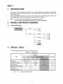
2.
MODELS AND MODEL NUMBERS
2.1
5.25inch FDD Series
Itlill
48TPI
-c
JA-551
JU-455
96TPI
JA-56X
JU-58X
.
-c
-c
JA-560
JA-561
JU-581
JU-585
JU-595
JU-465
~~~1~lgtl!l:l~111[
3.
SPECIAL TOOLS
The following special tools are used for FDO maintenance.
Table 3 - 1
Special Tools
Part No.
Tool
5.25 inch (48TPI)
JA-551/ JU-455
Exerciser
ilil!l l !i!l!il il !I I! !I! il! I! ! !I!I ! !I !I ~1!lj!~I!f~I! ~!iI JI!I! !I!l ! I! !I! I! i! !l il! i! !i! ! ~l!l!i! ! !
JA-561/ JU-465
Quantity
i!l!lil!9fiilllrl~lllgI111~!11!1
FOD-EXT-35
Alignment diskette
Data diskette
817-128
817-560
1-2
2D
2DO
1-2
Oscilloscope (50 MHz)
Probe(10: 1)
3
Frequency counter
Note:
*~:
Stand for the same as left.
-1 -
4.
OUTLINE OF MAINTENANCE
•
4.1
The following tools are required for maintenance of an FDD.
Alignment Diskette
Alignment diskette is used for head actuator alignment and index sensor adjustment.
Use the right diskette as shown in Table 8.1.
4.2
Exerciser
The exerciser enables you to make all adjustments and inspections necessary for an FDD.
functions include the following.
(1) Seek increment or alternate tracks
(2) Read (but no data compare)
(3) Write 1For2F(AII "O"sor"1"s)
(4) Head load (5.25inch FDD with optional head loader)
(5) Recalibration to track 0
The exerciser has switches and indicators to execute a specified function.
5.
DIAGNOSTIC PROCEDURES
5.1
Error Symptom Recognition
Its
Errors that occur because of the wrong operating procedure, wrong programming, the use of a
defective diskette, or soft errors due to external causes, such as contaminated air and random
electrical noise, are often attributed to an FDD failure.
Unless a visual inspection of the FDD reveals an evident assembly fault or a defect, always confirm
errors with another good diskette, and another known good FDD.
5.2
Soft Error Detection and Correction
Soft errors are normally caused by the following.
(1)
(2)
(3)
(4)
(5)
(1)
(2)
(3)
(4)
5.3
Contamination between read/write heads and diskette. This kind of contamination can be
easily eliminated by the liner in the diskette. Please follow the appropriate procedures
provided with the cleaning diskette.
Random electrical noise, normally a few microseconds or less.
Small defects in written data and/or track not detected during write operation may cause
soft errors during read.
Faulty grounding of the FDD or host system can also cause soft errors.
Wrong motor speed is another cause of soft errors.
Take the following steps on the controller side to recover from the soft errors mentioned
above.
Read the track again ten times or until the data is recovered.
If step (1) above fails to recover the data, access the adjacent track. Then return the head to
the original track.
Repeat step (1).
Any error that cannot be corrected by the above procedure is irrecoverable.
Write Error
If an error occurs during write operation, it is usually detected during the next revolution by
performing a read operation called write check. To correct an error, write again and repeat a
write check operation. If the result is unsatisfactory after ten or more write operations, perform a
read operation on another track to determine whether it is the diskette or the drive that is wrong.
If an error persists, replace the diskette and repeat the above procedure.
If the error still persists, assume the FDD defective. If the error is corrected, the diskette is
defective. It can be thrown away.
- 2-
5.4
Read Error
Most read errors are soft errors. Data can be recovered by following the recovery procedure in
section 5.2.
5.5
Seek Error
Seek errors are caused by the following.
(1)
(2)
Stepper motor or stepper motor drive circuit is faulty.
Faulty Carriage
There are two ways to recover from a seek error. One is to recalibrate to track 0, and seek
back to the original track. The other is to read the ID field, check the track number on which
the head is located, and move the head away from it. Read it again.
5.6
Interchangeability Error
Data which is written by one FDD may not be read by another. This error is called a
interchangeability error, which can be caused mostly by the following reasons, which should be
checked as follows.
(1)
(2)
(3)
(4)
Head misalignment: Refer to Adjustments and Confirmation section 9.6.
Head output too low: Refer to Confirmation section 9.3.
Motor speed difference: Refer to Adjustments and Confirmation section 9.1.
Format incompatibility.
6. TROUBLE ANALYSIS
To determine the cause of trouble whether it lies in the FDD, diskette, or controller, replace the
diskette and the FDD with good ones. If the FDD is assumed faulty as a result, follow the
procedure below.
6.1
Trouble Analysis Procedure
FDD trouble may occur in any of the following ten forms.
(1)
(2)
(3)
(4)
(5)
(6)
(7)
(8)
(9)
(10)
Index detection failure
I/O 34pin signal failure (Disk Change / Ready / Media In / Media Out)
Track 0 undetectable
No seek
No write
No read
Read error
IN USE LED won't light.
Write protect undetectable
No head load (S.2Sinch FDD with optional head loader)
Check with the troubleshooting flowchart in section 6.2.
CAUTION:
Be sure to switch the power off before removing an FDD or PCB from the operating system.
- 3-
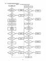
6.2
Troubleshooting Flow Chart
Table 6 - 1 Troubleshooting Flow Chart
Diskette
Defective
Check Item 5,
Table 6-2
Controller
Defective
Check Item 6,
Table 6-2
Run the operating system and
check. Record all diagnostic
information on tracks and sectors
as far as the program permits.
PowerSW
DCSWOn
Drive Select SW
Head load SW
On
Check Item 1,
Table 6-2
Check Item 7,
Table 6-2
Check Item 2,
Table 6-2
Check Item 8,
Table 6-2
Check Item 3,
Table 6-2
Check Item 9,
Table 6-2
Check Item 4,
Table 6-2
Check Item 10,
Table 6-2
YES
-4-
6.3 Trouble Analysis Table
Table 6-2
Trouble
Item
..
2
3
4
5
6
7
8
I/O 34pin signal failure
3
Track 0 detection failure
4
No head loading
2
2
2
3
4
5
No seek
2
3
6
No write
2
3
4
5
6
7
No read
2
3
4
8
Read error
2
3
4
5
6
7
8
9
10
11
12
9
10
IN USE LED
won't light
Write protect
failure
Cause
No.
Index detection failure
2
Trouble Analysis
2
2
Collet part faulty
Drive motor control PCB
Drive motor faulty
Index LED faulty
Index detector faulty
Index LED/index detector installation faulty
PCB motor on circuit
PCB index detection circuit
See Item 1.
PCB disk chanQe / ready / Media in / Media out ciuciit
Track 0 assembly
PCB track 0 detection failure
See Item 1.
See Item 2.
Head load solenoid
PCB head load ci rcu it
Stepper motor
Guide shaft contamination or damaQed
PCB stepper driver circuit
See Item 1.
See Item 4.
Head disconnected
Head shorted
Head load bail height wrong
PCB write circuit
See Item 1.
See Item 4.
See Item 6.
PCB read circuit
See Item 1.
See Item 4.
See Item 7.
Alignment
Azimuth
Index burst
Asymmetry
Limiter
Track 0
Head load time
Index neriod
PCB read ci rcu it
LED part
PCB IN USE circuit
Write protect part
Write protect circuit
-5-
7.
PREVENTIVE MAINTENANCE
No preventive maintenance is necessary for any FDD under normal conditions.
However if adjustments are necessary, the procedures in this manual must be followed.
•
(1)
(2)
(3)
Adjustments (Refer to Table 8-1)
Make a read/write head radial adjustment at the specified track. (Sides 0, 1)
Make an index burst adjustment at the specified track. (Sides 0, 1)
Make an azimuth measurement at the specified track. (Sides 0, 1)
CAUTION
Do not write when using alignment diskette. Check that write protect sensor is properly operating
with a data diskette.
Note:
8.
Section 9 describes the adjustment procedure in detail.
SPECIFICATIONS
Table 8-1
.
Specifications
MINI (a) type
Drive motor is dual speed type.
Item
Parameter
1
2
3
4
5
6
7
8
9
10
.
Head load time
MINI ((3) type
Drive motor is fixed speed type. (360 rpm)
Item
Parameter
jjI~j::j~jj;~j!~;jj!~j~~~jj~~j:I::~:~~j~j:II~j:!~:I:(~I;!j:~~j:1::~j~I;::)!j::iI:::::J1:ljtj:l:Y:::EI?!;;4:lfe@;~::j:i:~~Ijj:/j~Ij::~~tiI:I:jj~:j:j~~:j:~~;::!:~I:~ti~j;~~j:)::j:ir:~~~~;~;j~:~j;:jtIj;~:j
'I:
';;\\~\jIj~~~~::]:j~[:~I\\~\j~\~\I\\~\~I'N'~~~lrfjnqg~, :\:tmt~\1\\j:::j\\:j~j):~~}\)\~t: ~:)::\\:~:j\~]Ij\j]~]\\;~~\j\\)\\~\\\\;:n\~V~~*j'::f.'Jng#@')]]])\~)\j)II\\\)~\j\\)]\~)j\\\~\\::)j]j;
;',;\j~II~~t~:: fI]~A¢~<jI::::;:It} .:j\~;~:~j\t~::~t :g$t,v.:':{:~t::;j~:;~:~I: ':i{:t:~:~I~~;:'j~ijl~~:::~~~~~:::~}~:::~:~:;: ';~~j:t:::~j:~::\:IMlt~tl::~~ttjjI ";: :
2
Index period
Output level
3
Modulation
4
5
6
7
Resolution
Radial AliQnment
Azimuth
Index burst
8
Track 0
9
Asymmetry
10
Head load time
;)t::?:t:rt::~,: 3.2trmftttt:::' :t::/I/}:df 1:~1%;' .;: : ,:.: ~:':'.' <::/J},::~;":::t':\fi" ;::)/':::'::::/f:::..' .)::~~:{~:):;:}:, :::~$t })} ::,::\r.:'.:.
.:'!:jI(1??':: ,.:~~jtIIIIt:} /t/? :::::}: ±{J ak:{',·,:.·::·::;i':,,·:, .:::;.}}(:::::::J/::wi: ':{'i:' .;;/ii:i; :,;:: .';?:::~::::'?:;::,;' ':::"....~. :,:~:,·/?:t : : : .~:
-6-
9. ADJUSTMENTS AND VERIFICATIONS
9.1
Motor Speed Verification (Index Period)
(1) Insert a diskette, run the motor, and clamp. Refer to the index period column of Table 8-1.
(2) Step to the specified track.
(3) Connect a frequency counter to the INDEX signal:
TP7
(4) Check that the frequency counter readings meet the specifications of Table 8-1.
9.2
Write Protect Verification
(1) Check that the exerciser's write protect lamp goes on and off as a diskette is inserted and
removed as specified in the table below.
Diskette with write protect
Diskette with write protect
hole open
hole closed
OFF
ON
(Not write protected)
9.3
( write protected)
Head Output Verification
Use a new diskette if possible to identify head failure for this check.
(1) Insert a good diskette.
(2) Run the motor.
(3) Step to the track specified in the output level column of Table 8-1.
(4) Connect the oscilloscope probe as specified below.
CH1
CH2
EXT
·:·:I \~ I~I!:I !I:I ~ :jl ~I~I!\:~:\.I: .I:~1 1 :! :.:
Invert channel 2 and select the Add mode.
Set vertical deflection to 10 mV/division and horizontal deflection to 20 ms/division.
(5) Write 2F (all "1"s) on the entire circumference.
(6) Check that the average output level meets the specifications of Table 8-1.
vaverage --
Vmax + Vmin
2
If it does not meet the specifications, refer to Item 7 of the Trouble Analysis Table.
-7-
9.4
Output Modulation Verification
Modulation is calculated by the following formula.
Modulation
= - V max -
Vmin
x100{%)
V max + Vmin
Using the value obtained in section 9.3, and check that the calculated value meets the
specifications of Table 8.1.
::;
±m4#¥4.!§BZ=±4i- Maximum voltage Value: Vmax
mll~¥.:::m:;:~;:;~::::~;;;m;{t== Average Voltage
:::;:;:;: .. :-:
Minimum Voltage Value: Vmax
..
::
Fig. 9-1
9.5
Modulation
Resolution Verification
(1) leave the oscilloscope in the same condition as mentioned in section 9.3.
(2) Resolution is calculated by the following formula.
Resolution =
average x 100 (%)
V, F average
(3) Check that the calculated val ue meets the specifications of Table 8-1.
9.6
V2F
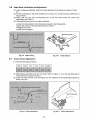
Radial Alignment Verification and Adjustment
Introduction
This adjustment is normally not necessary.
If the mounting screws for the stepper motor loosen, or if parts become defective, or if a
compatibility error occurs, check and readjust according to the following procedure.
Steps(4) to (9) below should be performed regardless of the type, CE or DAD alignment diskette
used. Use an alignment diskette suitable to the type of FDD to be adjusted according to Table 3-1.
(1) Insert Panasonic alignment diskette.
CAUTION:
Be sure to leave the alignment diskette under room conditions for 20 minutes before
adjustment.
(2) Step to the track specified in the radial alignment column of Table 8-1.
(3) leave the oscilloscope in the same condition as mentioned in section 9.3.
•
Cats Eye System
(4) Check the output waveforms for sides 0 and 1. They should appear as in Fig. 9-2.
(5) The two waveforms should appear in the amplitude ratio in the radial alignment column of
Table 8-1 or better.
(6) If the specified ratio is not satisfied, loosen the two mounting screws for the stepper motor.
-8-
(7) Move the stepper motor along the base by hand until the two waveforms assume
approximately the same amplitude, and retighten the mounting screws. (See Fig. 9-2.)
(8) Step the head outward (track 0) and inward (track 79), and confirm that the adjustment has
been completed.
(9) After the radial adjustment, be sure to confirm track 0 sensor adjustment as described in
section 9-9.
Note:
-
Alignments on sides 0 and 1 are adjusted at the factory. If they are misaligned, adjust
them to meet the specifications of Table 8-1.
==
==
when A > B
AB
x 100(%)
when A < B
A
-B- x 100(%)
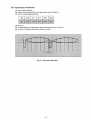
Fig.9-2 Radial Alignment Waveforms (CATS EYE)
9.7
Fig.9-2-1 Stepper Motor Mounting Screws
Azimuth Verification
(1) Insert an alignment diskette. Seek to the track specified in the azimuth column of Table 8-1.
(2) Set the oscilloscope in the same conditions as in section 9.3, and set horizontal deflection to
0.5 ms/division.
(3) Measure as shown below.
(4) Confirm that the measured value meets the specifications in the azimuth column of Table 8-1.
c
c
D
D
When B=C
Azimuth = 0'
When B>C
Azimuth = B - C
B-D
When B<C
x (A)
Azimuth = C- B
C-A
x (A)
(A): 12'
Fig.9-4 Azimuth Waveforms
-9-
9.8
Index Burst Verification and Adjustment
(1) Insert an alignment diskette. Seek to the track specified in the index burst column of Table
8-1.
(2) Set the oscilloscope in the same conditions as in section 9.7, and set horizontal deflection to
SOps I division.
(3) Check that the time from oscilloscope start to the first data meets the index burst
specifications of Table 8-1.
(4) If the specifications are not met, adjust as follows.
• Loosen the index detector mounting screws enough to free the assembly.
• Adjust the timing to meet the specifications of Table 8-1 .
• Retighten the screw.
• Check the timing again.
Fig.9-5 Index Timing
9.9
Fig. 9-5-1
Index Detector
Track 0 Sensor Adjustment
(1) Set the oscilloscope as follows.
TRIG
SYNC
CH 1
CH2
VERT
HORIZ
(2) Step between specified tracks at in the track 0 item of Table 8-1. (Turn the seek delay switch
on the exerciser to adjust 3 ms seek.)
(3) Loosen the track 0 sensor screw and adjust until the waveform on the oscilloscope appears as
shown in Fig. 9-6.
Fig.9-6 Track 0 Waveform
Fig. 9-6-1
-10-
Track 0 Adjustment
9.10 Asymmetry Verification
(1) Insert a work diskette.
(2) Step to the track specified in the asymmetry item of Table 8-1.
(3) Set the oscilloscope as follows.
TRIG
SYNC
CH 1
CH 2
VERT
HORIZ
:1:1~!1 1:·~1;1 1 !1 ~·.1 . !:l jl~:!~I !I !~! !~!':1 : I~.! .I !·I !: .!I:~:I I[!I:I·I !I:I.I !~!jl~j·: ;1·!:I!I ~I !I:! I·~[I:!~I.I~I·I !I!·:!I.il:I I: I~I.j·
(4) Write 1F.
(5) A read waveform is displayed on the oscilloscope as shown in Fig. 9-7.
(6) Confirm if it satisfies the value as shown in Fig. 8-1.
Fig.9-7 Asymmetry Waveform
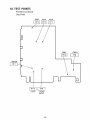
10. TEST POINTS
Printed Circuit Board
(Top View)
•
-12-
11. PANASONIC ALIGNMENT DISKETTE
Table 10·1
Panasonic Alignment Diskette
TPI
Part No.
Index
Burst
Azimuth
Radial
Alignment
Model
48
817-128
34TRK
34 TRK
16TRK
JA-551
JU-455
·13·
PART. II
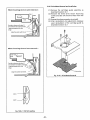
12. REMOVALS AND INSTALLATIONS
12.1
PCB Removal and Installation
ICaution of the cable leading
(1) Remove the four shield plate mounting screws
and take out the shield plate.
(2) Remove the one PCB mounting screw.
(3) Disconnect the connectors (J3 CON, J4 CON, J5
CON, J7 CON, J8 CON) from the PCB.
(4) To reinstall, reverse the above procedure.
(5) Readjustment is not necessary after PCB
replacement.
Let the cable pass under the C guide.
T
Do not let the pig
tail bitten or
disconnected.
If
Hook the cable to the
rib projected on the
base.
The cable shall not
protrude above
the upper face of
the drive. (Make it
flat by pressing
with a finger.)
Do not damage or
disconnect the pig
tail by pressing it
forcibly into the
' - - - - much in the PCB.
PCB
Fig.12-1-2 Cable Leading
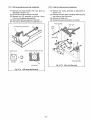
12.2
Front Plate and Handle Removal and
Installation
(1) Operate the lock cam of the clamp assembly,
and turn the clamp handle in the direction of
clamping.
(2) Remove the clamp handle.
(3) Remove the two front plate mounting screws,
and take off the front plate.
(4) Reverse the above procedure to reinstall.
Lock Cam
Fig. 12-1
PCB Removal
Clamp Handle
Fig.12-2 Front Plate and Handle Removal
-14-
12.3
Track 0 Sensor Assembly Removal and
Installation
12.4
(1) Remove the shield plate as described in section
12.1 step (1).
(2) Disconnect the J3 connector from PCB.
(3) Draw out the pins the track 0 sensor assembly
from the following locations on the J3
connector: N02, 4, 6.
At that time, draw out the pins with lifting the
stopper on the connector.
(4) Remove the track 0 sensor assembly mounting
screw and take out the track 0 sensor assembly.
(5) Reverse the above procedure to reinstall.
(6) After reinstallation, adjust the track 0 sensor as
described in section 9.9.
(1) Remove the cartridge guide assembly as
described in section 12.7.
(2) Remove the lifter unit as described in section
12.12
(3) Remove the collet assembly from the guide
shaft.
(4) Reverse the above procedure to reinstall.
(5) After reinstallation, perform collet assembly
center adjustment.
(6) Collet assembly center adjustment.
a) Temporarily fasten the cartridge guide
assembly.
b) Insert a diskette or dummy diskette and
clamp it.
c) Clamp repeatedly a few times to find a
good fit between the collet and the inside
diameter of the drive motor.
d) Bind the screws of the cartridge guide.
e) Check step c) again, if not good repeat step
a) through d) until the correct center
adjustment is achieved.
Track 0 (Blue)
Track 0 (White)
Track 0 (Yellow)
Stopper
Collet Assembly Removal. Installation and
Adjustment
t
-~
1)0
Collet Assem bly
Fig.12-4 Collet Assembly Removal
Fig. 12-3
Track 0 Sensor Assembly Removal
~,15
-
12.5
12.6
Clamp Assembly Removal and Installation
(1) Remove the front plate as described in section
12.2.
(2) Remove the shield plate as described in section
12.1 step (1).
(3) Remove the two clamp assembly mounting
screws and take out the clamp assembly.
(4) Reverse the above procedure to reinstall.
Write Protect Sensor Assembly and Index
Sensor Assembly Removal and Installation
(1) Remove the shield plate as described in section
12.1 step (1).
(2) Disconnect the J3 connector from PCB.
(3) Draw out the pi ns of the write protect sensor
assembly from the following locations on the
13 connector: N09, 11.
At that time, draw out the pins with lifting the
stopper on the connector.
(4) Draw out the pins of the index sensor assembly
from the following locations on the J3
connector: NoS, 7.
At that time, draw out the pins with lifting the
stopper on the connector.
(S) Remove the write protect sensor mounting
screw and index sensor mounting screw
respectively.
(6) Reverse the above procedure to reinstall.
(7) When reinstalling the write protect sensor,
exercise care so that the leads and write protect
sensor will not project from the bottom and
side of the base.
(8) After index sensor installation, adjust the index
burst as described in section 9.8.
Clamp Assembly
Fig.12-5 Clamp Assembly Removal
-16-
12.7
@
(1) Remove the PCB as described in section 12.1.
(2) Remove the handle and front plate as
described in section 12.2.
(3) Remove the clamp assembly as described in
section 12.5.
(4) Remove the write protect sensor mounting
screw.
(5) Remove the three cartridge guide mounting
screws and take out the cartridge guide
assembly.
(6) After reinstallation, adjust the collet assembly
as in section 12.4 step (6) and adjust the index
burst as in section 9.8.
(7) When removing or reinstalling, be careful not
to damage the carriage arm with the lifter.
Index Sensor (Orange)
Index Sensor (Red)
' - - - - Write Protect Sensor (Black)
'------- Write Protect Sensor (Green)
@
Cartridge Guide Assembly Removal and
Installation
Index Sensor
©
Fig.12-7 Cartridge Guide Assembly Removal
Fig.12-6 Write Protect Sensor Assembly and
Index Sensor Assembly Removal
-17-
12.8
Stepper Motor Assembly Removal and
Installation
(1) Remove the head carriage assembly as
described in section 12.9.
(2) Remove the two stepper motor assem bl y
mounting screws.
(3) Remove the stepper motor and stepper motor
stopper.
(4) Reverse the above procedure to reinstallation.
(5) After reinstallation, adjust the radial alignment
and track 0 sensor as described in section 9.6
and 9.9.
Stepper Motor Assem bly
12.9
Head Carriage Assembly Removal and
Installation
(1) Remove the PCB as described in section 12.1.
(2) Remove the one pig tail clamp mounting screw.
(3) Remove the two guide rod clamp mounting
screws.
(4) Remove the head carriage assembly, guide rod
clamp, guide rod, and pig tail clamp.
(5) Pull out the guide rod from the head carriage
assembly.
(6) Reverse the above procedure to reinstall.
(7) After reinstallation, adjust the radial alignment
and track 0 sensor as described in section 9.6
and 9.9.
Head Carriage Assembly
Fig.12-8 Stepper Motor Assembly Removal
Fig.12-9
-18 -
Head Carriage Assembly Removal
IPig tail leading
Pig Tail Clamp
(1) Pass the pig tail through the pig tail clamp.
(See Fig. 12-9-1.)
(2) locate the side 0 to the outer side and side 1 to
the inner side, provide a clearance of 1mm
between them, and place them parallel to each
other.
(Avoid twisting or closing.)
(3) Fig. 12-9-2
[When the carriage is on the outer-most track]
(a) When the head carriage is on the outermost track, lead the side 0 and side 1 along
line A on the pig tail clamp.
(b) Ensure that the pig tail does not come in
contact with the inner wall of the base.
(Contacting of the pig tail is allowable if
the side 0 and side 1 are not overlapped
each other vertically.)
(4) Fig. 12-9-2
[When the carriage is on the inner-most track]
(a) When the head carriage is on the innermost track, lead the side 0 and side 1 along
line B on the pig tail clamp.
(5) Provide a clearance of about 1mm between the
side 0 and side 1.
(6) Ensure that there is not excessive load or
protrusion at the outlet for the pig tail in the
head carriage.
(7) Fasten the pig tail clamp with screw.
(8) Do not pull the pig tail by a force more than
500g after it has been clamped.
(9) Pull the pig tail lightly to ensure that it does
not move.
Fig. 12-9-1
..19-
Mounting of the Pig Tail Clamp
12.10 Drive Motor Removal and Installation
When the carriage is on an outer-most track:
(1) Remove the cartridge gu ide assembly as
described in section 12.7.
(2) Remove the three drive motor mounting
screws and take off the drive motor from the
base.
(3) Reverse the above procedure to reinstall.
(4) After reinstallation, the adjustments necessary
upon reinstallation of the cartridge guide as
described in section 12.7.
c:::)
Outer-most
..._ - - track
Provide a clearance of about 1mm between the Side 0 and Side
1 approximately within this
range.
Align the center with line A. - - - - 0
When the carriage is on an inner-most track:
Inner-mos~
track
~
Provide a clearance of about 1mm between the Side 0 and Side
1 approximately within this
range.
Fig.12-10
lineA
Line B
Fig.12·9·2 Pail Tail Leading
·20·
Drive Motor Removal
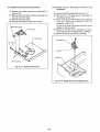
12.11 LED Assembly Removal and Installation
12.12 Lifter Unit Removal and Installation
(1) Remove the clamp handle and front plate as
(2)
(3)
(4)
(S)
described in section 12.2.
Disconnect the J8 connector from PCB.
Remove the LED assembly by sliding it slant
from the cartridge guide assembly.
Reverse the above procedure to reinstall.
The LED can be removed and installed as it is.
(1) Remove the clamp assembly as described in
section 12.5.
(2) Remove the lifter shaft clamping retaining ring
and draw out the lifter shaft.
(3) Remove the lifter unit.
(4) Reverse the above procedure to reinstall.
Retaining Ring
Lifter
\
Shaft
...\
"yJ,I
Lifter Unit
I'
"
lifter Spring
~0~
rr~~
~~~
Notch section
~
(Holder)
+
D
Clamp Assembly
(LED)
Lib
Fig.12-12 Lifter Unit Removal
[LED Front]
Fig. 12-11
LED Assembly Removal
- 21 -
12.13 Media Lifter Removal and Installation
12.14 Media Sensor Assembly Removal and
Installation
(1) Remove the clamp assembly as described in
section 12.5.
(2) Remove the lifter shaft clamping retaining ring
- draw out the lifter shaft.
(3) Remove the media lifter.
(4) Reverse the above procedure to reinstall.
(1) Remove the PCB as described in section 12.1.
(2) Remove the cartridge guide assembly as
descri bed in section 12.7.
(3) Draw out the pins of the media sensor assembly
from the following locations on the J3
connector: NoB, 10, 12.
At that time, draw out the pins with lifting the
stopper on the connector.
(4) Remove the media sensor assembly mounting
screw and take out the media sensor assembly.
(5) Reverse the above procedure to reinstall.
Cartridge Guide
Lifter Shaft
~
Fig.12-13
Media Lifter Removal
Fig.12-14 Media Sensor Assembly Removal
- 22-
13. EXPLODED VIEW
[JU-475-4AGG]
y;
~,
/.\
..~
L
* Caution: For transportation, insert the dummy diskette in the drive unit and close the lever.
Remove the dummy diskette before use of the drive unit.
;. 23-
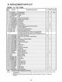
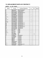
14. REPLACEMENT PARTS LIST
MODEL: JU - 475 - 4AGG
Ref.
No.
Part No.
Part Name & Description
Pcs
*RSP Remarks
1
NLA
PCB Assembly
2
1
Stepper Motor
1
Faston
1
2
LED
2
Clamp (For Guide Rod)
1
Stepper Motor Stopper
1
Shield Plate
1
Guide Rod
1
3
Front Panel
1
Clamp Handle
3
1
2
Head Carriage Assembly [YTUF47HD4-M]
1
2
Track 0 Assembly
2
Screw (For Guide Rod Cla.mp)
Screw (For Stepper Motor)
2
17
Screw [PCB Assembly (1), Faston (1), Front Plate (2),
Drive Motor (3), Pig Tail Clamp (1), Shield Plate (2),
Cartridge Guide (4), Clamp Bearing A (2), Media Sensor (1)]
2
Screw (For Shield Plate)
16 YTF1E00310B4
2
17 YTF1E00300B4
Screw (For Track 0 Sensor, Index Sensor)
1
18 YTF3L 12930B2
Base
1
2
19 YTUF5DMT~3BT Drive Motor [FMD01732B4T]
1
20 YTF1G01482B3 Pig Tail Clamp
1
22 YTF7K14480B4 LED Holder Assembly
1
23 YTF3C07194B3
Lifter
1
24 YTF3C10760B3
Media Lifter
2
25 YTF4HO 1360B4 Lift Shaft
1
26 YTF4H03109B3 Clamp Cam Assembly
1
27 YTF4JO 190 1B4
Lift Spring
1
28 YTF4J03500B4
Media Lift Spring
CollefAssembly
1
2
29 YTUF52CLT
1
2
Write Protect Sensor
30 YTUF45WP8
2
Retaining Ring
31 XUC2
2
32 XUC3
Retaining Ring
1
Lock Cam
33 333D36817693
1
34 333D46624770
Lock Spring
1
35 333D46817500
Pad A
1
Cartridge Guide
36 YTF2E12870B1
1
37 YTF4F03424B4
Clamp Bearing B
1
38 YTF4F03435B2
Clamp Bearing A
1
39 YTF2F12940B4
Pad B
40 YTUF451DX8
2
Index Sensor
1
1
2
41 YTUF47MS4
Media Sensor
42 YTF8C02302B4
Dummv Diskette
1
*RSP
: Recommend ~ervice e.artsper 1,000 Units.
Caution : 1. PCB assembly with mark (NLA) is no longer available after production discontinuation of the
complete set.
2. Whenyou order the aforementioned parts, be sure to specify "Part No." of the parts
ordered.
1
2
3
4
5
6
7
8
9
10
11
12
13
14
15
YTUF47PK4
YTFMD02700B4
YTFJC00521 B4
LN41YPHL
YTF2C07161B4
YTF2C08722B3
YTF2H 12862B2
YTF4H03091 B4
YTF5W03272B2
YTF6AO 1092B3
YTUF47HD4-T
YTUF45TRK8
XSB3 + 4FX
XSB3 + 5FX
XSB3 + 6FX
- 24-
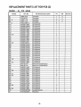
15. REPLACEMENT PARTS LIST FOR PCB (1)
MODEL: JU - 475 - 4AGG
Ref.No.
C2
C3
C4
C5
C6
C7·8
C9
C10
C11 . 12
C13
C14
C15·16
C17
C20·21
C25·26
C27
C28
C29
C30
C31
C32
C34
D1
D2·3
D4
D8·9
D12·13
IC1
IC2
IR1
J2
J3
J4
JS
J7
J8
L2
L3
L4·5
L6
L7 ·8
Part No.
ECEA 1EKS330E
SR585F105Z
MCH215F103ZK
ECEA 1EKS330E
MCH212F104ZK
FCCOO320B821
MCH215A271JK
MCH215C102KK
FCCOO320B223
MCH215A391JK
MCH215A 101JK
MCH215F223ZK
MCH212F104ZK
FCCOO330B103
MCH212F104ZK
ECEA 1EKS330E
MCH212F104ZK
ECEA 1EKS330E
MCH212F104ZK
ECEA 1EKS330E
MCH215F103ZK
MCH212F104ZK
MA1S1WK-TX
MA122-TX
MA121-TX
DA 116-T96
MA1S7-TX
FQL01280B4
HA 13421 PMP
RYLA6J102
FJCOO450B401
FJC0121 OB4
08052539
SOSB-DR
S04B-DR
S02B-DR
FBR06HA8S0NA
SFC24050202
NL322522-181
NL322522-680
EL.EPG~~OKA
Part Name & Description
Electrolyte Capacitor
Ceramic Capacitor
Chip Capacitor
Electrolyte Capacitor
Chip Capacitor
Chip Capacitor
Chip Capacitor
Chi p Capacitor
Chip Capacitor
Chi p Capacitor
Chip Capacitor
Chip Capacitor
Chip Capacitor
Chi p Capacitor
Chip Capacitor
Electrolvte Capacitor
Chi p Capacitor
Electrolvte Capacitor
Chip Capacitor
Electrolyte Capacitor
Chip Capacitor
Chip Capacitor
Diode
Diode
Diode
Diode
Diode
LSI
LSI
Block Resistor
Connector
Connector
Connector
Connector
Connector
Connector
Choke Coil
Choke Coil
Choke Coil
Low-Frequency Coil
Choke Coil
-25 -
Pcs
1
1
1
1
1
2
1
1
2
1
1
2
1
2
2
1
1
1
1
1
1
1
1
2
1
2
2
1
1
1
1
1
1
1
1
1
1
1
2
1
')
RSP
2
2
Remarks
REPLACEMENT PARTS LIST FOR PCB (2)
MODEL :JU - 475 - 4AGG
Ref.No.
01
02
Q5·8
06
R1-9
R10
R11
R12
R13
R15
R16
R18 - 20
R21
R22
R23
R24
R25·26
R28
R29
R30
R31
R32
R33
R34
R35
R36
R37 - 39
R40
R41 ·42
R43
R44
R45
R46
R47·48
R49
R50·51
R52·53
R54
R55
R56
R57
R58
R59·60
R61
R62·63
VR1
IX1
Part No.
Part Name & Description
Pcs
RSP
2
2
2
2
XN4212-TX
3SK144-TX
UN2211-TX
UN2111-TX
FRA00100B151
ERJ6GEYJ392V
ERJ6GEYG392V
ERJ6GEYG512V
ERJ6GEYJ392V
ERJ6GEYJ392V
ERJ6GEYJ104V
ERJ6GEYJ 163V
ERJ6GEYJ822V
ERJ6GEYJ821V
ERJ6GEYJ392V
ERJ6GEYJ331V
FRA00100B151
ERJ6GEYG363V
ERJ6GEYG203V
ERJ6GEYG363V
ERJ6G EYG203V
ERJ6GEYG363V
ERJ6GEYG203V
ERJ6G EYG363V
ERJ6GEYG203V
ERJ6GEYJ392V
ERJ6G EYJ102V
ERJ6G EYJ163V
ERJ6G EYJ362V
ERG1SJ271V
ERG1SJ151V
ERJ6GEYJ104V
ERJ6G EYOROOV
ERJ6GEYJ471V
ERJ6GEYJ822V
ERJ6GEYJ393V
ERJ6GEYJ182V
ERJ6GEYJ221V
ERJ6GEYJ273V
ERJ6GEYJ473V
ERJ6GEYJ392V
ERJ6GEYG203V
ERJ6GEYJ102V
ERJ6GEYJ4R7V
ERJ6GEYJ392V
PK502 H203 HOD
Transistor
Transistor
Transistor
Transistor
Chip Resistor
Chip Resistor
Chip Resistor
Chip Resistor
Chi p Resistor
Ch i p Resi stor
Chip Resistor
Chi p Resistor
Chip Resistor
Chip Resistor
Chip Resistor
Chi p Resistor
Chip Resistor
Chip Resistor
Chip Resistor
Chip Resistor
Chip Resistor
Chip Resistor
Chip Resistor
Chip Resistor
Chip Resistor
Chip Resistor
Chip Resistor
Chip Resistor
Chip Resistor
Metal Film Oxide Resistor
Metal Film Oxide Resistor
Chip Resistor
Chip Resistor
Chip Resistor
Chip Resistor
Chip Resistor
Chip Resistor
Chip Resistor
Chip Resistor
Chip Resistor
Chip Resistor
Chip Resistor
Chip Resistor
Chi p Resistor
Chip Resistor
Variable Resistor
1
1
2
1
9
1
1
1
1
1
1
3
1
1
1
1
2
1
1
1
1
1
1
1
1
1
3
1
2
1
1
1
1
2
1
2
2
1
1
1
1
1
2
1
2
1
EFO-Gr~,()~rl1.
D",.. "".,~tnr
1
• 26·
Remarks
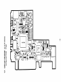
16. SCHEMATIC DIAGRAM
[JU-475-4AGGl
TPS
SIDE 0 R/W 2
~
R41
CliM
3.6K
+SVA
RSO
+5V
R51
39K
39K RS2 1.8K
L2
FERRITE
R22
IVW 1 ~~---------:=--r-;;:;t;;;;;:;;~---t--4-----,
5
820
C11 0.022..LJ
R49
8.2K
+ 5 V RETURN -¥r"-----.--4--t~r...,-.;.~
C'20.022)J
SIDE 1
+ 1 2 V RETURN ~t~~"---e--'-"'~
COM
R/ W 1
---'\I+r.;.;;;...--;~----t------+----:::----+--+---.~--,.
ERASE
~,I+J-~--'-----+--f..1
GND
NC
FG
+ 12 V 0 C ---".£,.....:.'---1
)t-...~---...~---.~
~
~
i'5V
-e
0
-
DRIVE
DRIVE
DRIVE
DRIVE
SELECT
SELECT
SELECT
SELECT
.0
U
CD
U
0
0
PHLA
DGND1
1
2
:5
NINDEX
NTRACKf)
NOS
4
NWPRO
HRDDT
NRDY
2
-INDEX
3
-TRACKllj'j
4
- WR IT E PROTECT
- READ DATA
- READY
6
8
RY
NODE SELECT
R23
NDMACT
11
MOSO
12
Ie 1
- MOTOR liN
DIRECTION SELECT
-STEP
- WRITE DATA..
- WRITE GATE
- S I DE SEL£CT
- IN USE / -HEAD LOAD
--t:==----J.--l-~___I__t_-l-~-!~~~ HMTRON
--*~--_t_------+-+-+--+-+-
r--\II~--4~t12V t'2V~
......----::~-----t 0 I RSEL
C34
NSTEP
~...a.;.---+--------+--+--+----lt----ill--t--~--~
","*~--+-----~--+-'--'-of-r--+----=-I
NWRDT
HWRC T
-*-=:..--_t_-----+-.----+-+~-_t_--~
NS I DESEL
~~---+------4-----+-+_+-+_---=.~
NH LI NU
NLO WHO
~------
--+-+-_+______1~fJWw....r;.z.l
INU
WVCC
B.2K
PWP
NIDX
MEDIA SENSOR PC
0
PTKD
N
PHSD
0
23
TRACK 00 PC
TRACK 0D PE
TRACK 0G LA
R24
9
L7 33lJH
HD1
STEP NOTDR
~-------~,~
16K
9
~
~~~'-=.L~2~:;r;.~0~. 1~lJ~_.!-m~ "u:~
\7
7 ' } - - - -.....
~--..a..:..t
IC2
27
2
rz'0~ HA13421PMP t-=2:.;.3-------..:.3..JV}~
NSD1
1 ....
6
NSD2 .-=-_ _..:..0
4
R21
WRITE PROTECT PC
WRITE PROTECT PE
INDEX PE
INDEX PC
0.0. MOTOR
O'
NSTPACT
R19 R20
16K
t3::~}
FQL01280B4
~:-=---+_------+-+-+--+""-"""-"'--fJYVrF::.t
+5V
:z:
26
M
~
0
0
:z:
27
:z:
29
x:
~
0
a:
0
~
0
w
...J
C
x:
c
N
0
z
...J
U
::t:
0
u
u
>
0
18
-
u
V)
10
+ 5V
......
~~I-
_ _- - J
IN USE LED
+12V
weND
N ouAV 30
u zu c:c
e2
u>AG
1
10 uu NO 350. jJ
(J')
20
16K
MA151A
19 22
~----'l----'f-:----Wlt---
4.7
+ 5V
~OTEL
o ~ NOT
o
RP1 -{>
INSTALLED
1Knx6
XTAL
MEDIA SENSOR PE
NEOlA SENSOR LA
NC
Ne
- 27-
DJ8
l.llCT~
~H&l~M~~
TP5 L6
2
08
K
H
A
J4 12
R49
, OH
G
I~
I F-=Ht:~
I
c:J
c:J
«
.
~
I
Ion
I" ..-.
qo C.
0
I
=>
.....
..... ........
~
c~'"Ccv
<tV;
01:
£:C cv
.- g
-
c.
U
0
::::> E
-
~u
U
.
r-..
~
H
0
co
<
:::l
-
~
C;rR~
+
C35"'Hu~NHI+IH C29 R3~~
1 1_
JP:J:
~~
JL ~IO
-
U R48 : r : : I C I 5
Ici
O!
C11 R46 028
~I
~I I
+
49
R30
I
~I
H
~I
I
FQL01280B4
0IR23
I
I
I
.
00
N
FPK04162B3
D5
~
1:1:~5=f~IHH ~ ~
II
16 C3D:J;.~/
..&- R18
-rI m"&-
84
1
DCTPl C
_
N
Rl._ R59
EC
D
____ ~-2N_~
R63_
R34
J5
I
....J
::t:
> A 09,
I I "'-R471 • I~K
I.,......rl::1
_
H
_..J
R36
a:
~~".
G
co
...--
u.
L4
a:
_ •
01 - -
a> _ _ - -
~
~ Cl3
C'f)
~
a>
. . . . .~
TT4 ~~~-so
a:
Cl0
I~CO
'R55~
~ R37a: OAC3 ~
II
..
I;;
[!]
:C34
::: IC2
C24
R21
C TP6
RPI
12
~~
3
0
!3
+02
:;;:
a: a:
Il!
Il!
Z
l(J
•
JI
3
a:
RY
6
1.
m.<or
T!:l D
R20
C5 ,
C231 +
R61 Q 4 R ;
Ii;
R25
I I I~
*1
~ ~~
0H-H4=1='04 3~c::~ .~3D-I.... 0
0H
lSI!!
R26
L20~
5VDC
..
J1
l=
2
l3
CI
1_J3
TP8
c;:;
r
GNOOl2V06I
ll
J2
_[ -
DC
-
I
-
;
1211
•
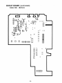
CIRCUIT BOARD [JU-475-4AGG]
Solder Side
(Bottom)
I I I
$ =
c:::-
I
"
I-
I I
r
•
o o o -t+H+H-
0
(Y)
CD
C\J
c...o
~
~
0
~
tI
0
r-
CI)
I
Q.
tZ
~
0LL
-H-H+
- 29-
~
~
MEDIA
TRACK 00
DETECTOR
DETECTOR
WRITE
STEPPER
PROTECT
MOTOR
~~©~~© jD~€
l...---
l...---
I
000
I
~UJ
~
m
I
(
I
\
r
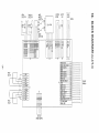
1
3
5
" " "
~~ ~
00 0
00 0
I I :t> m "
00
mm
mm x x
::::::j::::::j
0<
0
\:l \:l -U \:l
:::0 ::0
00
"'-J
11
2
\
/"'""\.
HEAD
(Side 11
~
~
I
I
I
7
9
4
m"
6
8
\ J 10
~ 12
UJ
I'.)~
~
-f
0
:::0
c..n c..n c..n
til
:J:: 3: 3: :J::
00 00
IJJ I'.)
-~
I'.)~
~
:l-j-I-;-'
til
l;)l
I
I
I
1
I
1
1
c:
m
"--I "- l
-0 -0
n
"m
J5
J4
J2
+ C"I C"I':'
V1Z Zl'.)
<0 0<
_
UJ
N
'\
.....
/
TO HOST
(POWER SUPPLYl
J7
II'.)~T
~
z~
7
Z
-
-
_
0
mm
GND
ERASE
R/W 2
COM
R/W 1
GND
m
m
r- -U -U - l - l
"
R/W 1
COM
RIW 2
ERASE
I
I
1
I
I
I
I
I
OPTION
I
I
+
+
C"I~ c..n V1 3:
zl'.) -0< 0
o
~
~
.
LOAD
I
U"l_ UJ I'.)
:z: ::z
w
HE AD
(Sid eOl
I
I
CO
I
- f - f - l ~~
»» »
»» »
r- -0 -0
I
I
I
0- _ I ' . ) ~\oO -....J V1
:::0 :::0 :::0 :::0:::0
00 0
00 0
:::0 :::0 :::0
~ ~
D.O. MOTOR
~
: HEAD
I
mm m
c..n c..n c..n
mm m
ZZ Z
c..n c..n c..n
LED
INDEX
DETECTOR
3: 3: 3:
:t>
ICD/ t
ACTIVITY
Ja-
I:J:~I
Ir-~I
I
I
I
I
I
I
I
I
1
)'9:
1 _____
MODE SELECT
-HEAD LOAD/-IN USE
-DRIVE SELECT 4
-INDEX
-DRIVE SELECT 1
-DRIVE SELECT 2
-DRIVE SELECT 3
-MOTOR ON
DIRECTION SELECT
J1 -STEP
-WRITE DATA
-WRITE GATE
-TRACK 00
-WRITE PROTECT
-READ DATA
SIDE SELECT
-READY/DRIVE STATUS
1...33 odd number
SIGNAL GND
2
4
6
8
10
12
14
16
18
20
22
24
26
28
30
32
34
TO HOST
(SIGNALl
Matsushita Communication Industrial Co., Ltd.
Memory Systems Division