1
SERVICE MANUAL
PC-ESOO
SHARP
CODE:OOZPCE500SM/E
MODEL
: Cursor shift, right/left(~.~)
Insertion (INS)
Delete (DEL, BS)
Line up, down (i, !)
Edit function
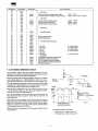
1. Product outline
PC-ESOO
The PC-E500 employs the large display (40 digits x 4 lines) and 32KB
memory (standard).
Serial 1/0 machine
2. Specifications
Communication
system
: Start-stop synchronous (asynchronous) system, half duplex/total duplex mode
Model name
: PC-E500
Communication
speed
: 300, 600, 1200, 2400, 4800, 9600bps (bit per
second)
Display
: 40 digits x 4 lines (5 x 7 dot matrix liquid crystal display)
Parity bit
: Even number, odd number, none
Calculation digit
: Single accuracy calculation; 10 digits (Mantissa)+ 2 digits (Exponent)
Double accuracy calculation; 20 digits (Mantissa) + 2 digits (Exponent)
In CAL, MATRIX, or STAT mode, calculation
is performed in single accuracy.
Calculation system
: In the sequence of formula. (Priority judgement function)
Program language
: BASIC
CPU
: CMOS 8 bit CPU
System ROM
: 128 K Byte
Memory capacity
: System area about 3.8 K Byte
Fixed variable (A- Z) area 312 Byte
Program data area 28600 Byte
Stack
: Total 145 Byte
Subroutine; 4 Byte for one stage
FOR-NEXT; 21 Byte for one stage
Basic calculation
functions
: Basic calculations;
Addition, subtraction, multiplication, division
Functional calculation;
Trigonometric function, reverse trigonometric
function, hyperbolic function, reverse hyperbolic function, logarithm, exponent, angle
conversion, power, power root, coordinate
conversion, extraction of the square root, integration, absolute value, code function, pi,
etc.
Word length
: 7, 8 bit
Stop bit
: 1 , 2 bit
Connector
: 15-pin connector (for connection with external
devices)
Output signal level
: C-MOS level (4- 6V)
Interface signal
: Input.; .... RD, CS, CD
Output ...... SD, RS, RR, ER
Others ...... SG, FG, VC
Memory protection
: Battery backup (Backups the program and
data when the power is turned off.)
Operating
temperature
: o-40·c
Power source
: DC 6V (R03 x 4)
Battery operating
time
: About 70 hours of continuous operation
(Under the operating temperature of 2o·c. 1O
minutes of calculation or program execution
and 50 minutes of display for every hour)
• There may be some variation depending on
the operating environment and using conditions.
Power consumption
: 0.07W
External dimension
: 200mm (W) x 1OOmm (D) x 14mm (H)
Weight
: 250g (Including the battery)
Accessories
: Hard cover, R03 battery x 4, Instruction
Manual
SHARP CORPORATION
This document has been published to be used for after sales
service only.
The contents are subject to change without notice.
-
PC-E500
3. System configuration
Pocket computer
PC-ESOO
Cassette interface
CE-124
·-----·- .....
•••••
••••• 1----------------1
••••••
1-.1...__________ ••••••
••••••
••••••••••••
_.....,__"""4~-1 =~·::::::::.
- --------1 •••••
Printer & cassette interface
CE-126P
Personal computer
MZ series, etc.
(The RS-232C
function is required.)
RAM card
CE-212M (SK Byte)
CE-2H1 SM (16K Byte)
CE-2H32M (32K Byte)
CE-2H64M (64K Byte)
*,
a cable
For section
corresponding to the
model is required.
Color plotter printer
CE-515P
Pocket disk drive
CE-140F
4. PC-E500 system block diagram
LCD LF7448G
[
DC-DC converter
J
Column (1)
Common
HD61202
HD61203
"
E4
MN1280 LB detection VDD
Q
IC
1IRQ~~--'--~__;A~D~R~R~A~O~--A_1_7
______,l
J~7t!'::.1--
.___v_1-_v_s_v_E_E_ _
Column (2)
1» 0
CEs
~ '---'--'-----======-°':_:::::::!:!==!::=:=:::::;-;:::=:==~~>I
__
E3
CPU
SC62015B01
Ceralock ~
2.30MG ~
('-~::D>=A·u~[A~1=<=D=7====::::'....1====~
I(,.
CEO - CES
KOO - K010
K10-K17
II-
T.____,__ _-1 1--i
....~
I- .___ _,,,_
b
...J
en
0
a:
<
(.)
:::?! :::?!
0<
a: a:
1--
ROM
RAM
HM62256
LH5320X1
CE2
CEO
r
r
11 pin
15 pin (SIO)
J
Key matrix
LFP
,____ __,I-
-2-
backup
battery
-
P C-E500
5. Memory map
SK RAM card
&H40000
32KRAM
card
64KRAM
card
16K,RAM L
card
J
&H43FFF
_L
J
l
&H41 FFF
&H47FFF
&H4FFFF
~
&HB8000
Built-in RAM
(32KB)
*
&HBFFFF
*
~
&HEOOOO
Built-in ROM
(128KB)
&HFFFFF
6. LSI description
CPU (SC62015) terminal signal description
Terminal No.
Signal name
Input/Output
1
2
3
4
5
X1
X2
X3
X4
VDD
Output
Input
Output
Input
Output
Power
Input
Power
Input
Input
Output
Input
Output
6
vcc
7
8
RESET
GND
TEST
Cl
9
10
11
12
13
14
15
co
ON
WR
MRQ
K10
-
Input
I
I
I
22
23
K17
DIOO
Input
1/0
I
I
I
30
31
DI07
AO
1/0
Output
I
I
I
49
A18
VDISP
VA
cpD
K015
K014
K013
K012
K011
K010
IRQ
Output
50
51
52
53
54
55
56
57
58
59
Output
Output
Output
Output
Output
Output
Output
Input
Signal description
Ceramic oscillation output
Ceramic oscillation input
CR oscillation output
CR oscillation input
Display power (converter) control output
EB power input terminal
Reset input. Reset at high level.
8power input terminal
Test input
Cassette signal input terminal
Cassette signal output terminal
ON key input terminal. Normally pulled down to low level.
Write clock. Normally high level.
.., (Not used.)
Key input terminal
Data bus
~
>
Address bus
}
(Not used.)
Clock output terminal for display chip
SIO PRQ (Not used.)
SIO ER, High level with OPEN command.
SIO RR (Reception in the main body side allowed)
} SIO RS (Send request in the main body side)
Key strobe signal
Low battery detection input terminal
-3-
-
P C·E500
Terminal No.
Signal name
Input/Output
60
61
62
63
64
65
66
67
68
69
70
71
72
73
cj>OUT
CE7
CE6
CES
CE4
CE3
CE2
CE1
CEO
cpA
DIS
HA
RD
K09
-
I
I
I
82
83
84
85
86
87
88
89
90
91
92
93
94
95
96
97
98
99
100
KOO
RXD
TXD
E15
E14
E13
E12
E11
E10
E9
E8
E7
E6
ES
E4
E3
E2
E1
EO
Output
Input
Output
Input
Input
Input
Input
Output
Output
Output
Output
Input
Output
Signal description
-
}
-
}
ROM card chip select signal (active high)
Chip select signal for display chip (Active high)
Output
Output
-
Output
Output
Output
-
-
Output
-
Output
Output
Input
Input
Input
(Not used.)
10000 - 1FFFF
00000 - 03FFF, 08000 - OBFFF
(Not used.)
Internal ROM chip enable signal
RAM card chip enable signal
Internal RAM chip enable signal
)
)
COOOO - FFFFF
40000 - 7FFFF
80000 - BFFFF
(Not used.)
Key strobe signal
SIO RD (Receive data)
SIO SD (Send data)
)
CE·140F data ;op"tt"mlnal
P-ch open output
P-ch open output
P-ch open output
P-ch open output
11 pin DIN
11 pin DOUT
11pin102
11 pin 101
11 pin ACK
11 pin BUSY
(Not used.)
Display power (converter) control signal
Low battery voltage control signal
SIO CS (Opponent side send enable)
SIO CD (Opponent side send request)
SIO PAK (Not used.)
P-ch open output
7. Low battery detection circuit
The PC-E500 is equipped with the low battery detection circuit. The
operations of the circuit are described below. (Part location numbers
may differ from those in the actual circuit diagram.)
R1
CPUIRQ
R2
When input voltage VIN exceeds the detection voltage VD, the output
of the voltage detection IC [LBIC(MN1280)] is driven from Low to
High. When VIN falls under VD, the output is driven from High to Low.
The LBIC (MN1280) detects both the CAU level and the STOP level
by dividing the voltage applied to the input terminal (2 pin) with R1
and R2 and by turnin_g on/off R2 with CAU signal of GA
When the power voltage falls under the CAU level, as shown in Fig.
3, the BATI symbol lights up. When the power voltage falls further
under the STOP level, the symbol goes off.
For CAU level detection, the CPU E3 it turned on (low level) and the
CPU IRQ terminal state is observed. (If the IRQ is at Low level, the
symbol lights up.)
CPU E3 - N-ch open
---"
BF
3'o---@N
GND
~ESET
(V)VIN
I
VDM
VOL
.=-°!:-
2.0V
I
T
VD
0.1-0.3V
0"--.._--'-~--"---<~
OUT
(V)
When the CAU level is detected, the CPU E3 terminal is turned off
(high impedance). (When the CPU E3 terminal is turned off, resistor
division is not performed and the voltage at LBIC 2 pin increases,
driving the output from Low to High.) The CPU IRQ terminal state is
checked again to detect the STOP level
Q)
g .b.9LQt:-! _-
o.,,,.___..___ _,__,___
L....JL.Oo,
Voltage detection IC
operational description
After the STOP level is detected, the ON key and the RESET key become ineffective.
Low battery detection circuit check
CAU level VCC - GND: 4.2V to 4.6V
STOP level VCC - GND: 3.8V to 4.2V
- 4-
1 --ym--CAU level
STOP level
Fig. 3
-
PC-E500
9-3. Battery replacement label attachment
8. Current consumption check
Power source:
DC +5.0V is supplied to 11-pin connector No.2 pin
(VCC) and
to No.3 pin (GND).
Current:
ON (BASIC mode">" is displayed); 3.24mA or less
OFF (Power off); 64µA or less
E
E
av
LSI circuit
SPEC(Max.)
ci
Actual use (Max.)
RUN
f·2304KHz
During display
OFF
4.2mA
220µA
3µA
<<<-
LH5320x1 (2Mb ROM}
RUN
HLT
1Ac-120ns
70mA
15µA
f-306KHz 4.59mA
HM62256LFP- 12SLT
(32KBRAM}
RUN
HLT
1Rc-120ns
70mA
100µA
f· 153kHz, 1.29mA
1.0mA
<-
500µA
100µA
15µA
<<<-
30µA
<-
SC62015B01 (CPU)
HD61203
f·600kHz
HD61202 (x2)
During access
during display
HLT
MN12800 (Low bettery detection IC)
Battery replacement caution label (A)
I I
TLABH1266ECZZ
<-
• Must be free from tilt.
<-
DC-DC converter (input)
1.2mA
<-
VDD
1.0mA
<-
DC power
5.0±0.1V
I
10
9-4. Shield tape attachment
Shield tape A
Bottom cabinet
GND
PC-E500
Note: When attaching to the boss
section, attach neatly
along the boss.
Shield tape
e
9. Note for servicing
~ omoob~ot
}
9-1. Battery holding cushion attachment
boss
Attachment procedure
Shield tape A
1) Remove the separation paper in side B, and bend section C and
D as shown below.
2) Fit the A side with the reference, and paste the B side.
Battery holding
cushion
Reference
3) Remove the separation paper, and attach the tape.
~-Fold.
Adhesives~<
Battery lid
4) Attach the three boss sections. {Fit the boss holes with the shield
tape holes.)
5) Attach the tape so that there is no slack.
Shield tape B
9-2. Battery holding cushion attachment
1) Bend E section. (Similar to C section.)
2) Fit with the reference and attach so that a1 and a2 are even.
3) Attach the boss section. {Fit the boss hole and the shield tape
hole.)
4) Attach the tape so that there is no slack.
Reference
A
9-5. Main PWB replacement procedure
CD Press the OFF key. (If a RAM card is installed, remove it.)
=
~ Switch the select switch from A to B.
@ Replace all the four batteries with new ones.
©
Bottom cabinet
Press the RESET switch.
@ Switch the select switch from B to A. {Install the RAM card.)
Battery holding cushion
-5-
-
PC-ESOO
9-6. Memory backup battery cover attachment
9-10. Battery replacement label B attachment
Card lid (inner side)
MEMORY BACKUP BATTERY REPLACEMENT
WHEN REPLACING THE MEMORY BACKUP
BATTERY. MAKE SURE THAT THE INSTALLED
OPERATING BATTERIES (TYPE-AAA • R03 X 4)
ARE NOT LOW
FOLLOW THE STEPS
(j) TO 0 AS SHOWN IN
THE FIGURE.
®
Hang the battery on the larger pawl.
Battery
replacement
label B
@ Push the battery to hang on the smaller pawl.
© Hang the battery cover pawl on the cabinet, and push it to attach.
<I» tighten the screw to fix.
!Reference
9-7. Memory backup battery replacement
• Must be free from tilt.
When replacing the memory backup battery, be sure to install four
batteries (R03 x 4). (Use unexhausted ones.)
9-11. Insulation spacer attachment
Replace the battery in
procedures (1) to (6)
as shown in the figure.
Battery terminal e
9-8. Terminal caution label attachment
1) Solder the battery terminal EE).
2) Take the insulation spacer with tweezers and insert under the battery terminal from side ®. (Note that the paste side is the battery
terminal side.)
9-12. lnsulatlon sheet attachment
Insulation sheet
©
~T0<m;no1-on
*
1"'91
Paste the label correctly in position.
• Attach the insulation sheet so that it does not cover the spring by
minimizing dimension A and maximizing dimension B.
9-9. Battery Insulation sheet attachment
Insulation sheet
Battery cover
A
A
Attach the insulation sheet to the center so that dimensions A (4 posi- 6 tions) are all the same.
-
PC-E500
(2)
10. Check software for servicing
Mask ROM check
MENU screen
• Check item
(1)
Liquid crystal visual check (alternate display)
(2)
Mask ROM verify check
(3)
Built-in RAM read/write check
ROM CHECK (WAIT 6 SEC)
(4)
11 pin 1/0 check
(5)
15 pin 1/0 check
(6)
RAM card read/write check
• Required tools
Jig UKOGC3020CSZZ: Used for (4) and (5).
Buzzer
(3times)
• Outline of using method
Before inputting a check software, clear the RAM completely.
When check (6) is executed, the RAM card content is deleted.
Save programs and data before check, if necessary.
<MENU>
1 : DISP 2: ROM 3: RAM
4: 11 PIN 5: 15PIN 6: CARD
OJ
Key input
0
Key input
y
Buzzer (Once)
ROM CHECK (WAIT 6 SEC)
ERROR!!
ROM CHECK (WAIT 6 SEC)
EX Ver. 1 (LH5320XH)
ROM CHECK OKI
..,.,.,- MENU screen
(1 ) DISP (display) check
0
MENU screen
(2) Mask ROM check
Key input
(3) Built-in RAM check
(3) Built-in ROM check
CD
Key input
0
Key input
MENU screen
(4) 11 pin check
0
(5) 15 pin check
0
RAM CHECK
Key input
(6) RAM card check
Note: To end a check, press the BRK[ON] key.
• Details of each check
(1)
DISP (display) check
Y
MENU screen
Buzzer
(3times)
Alternate display
All symbols light up.
Buzzer (once)
RAM CHECK ERROR!!
RAM CHECK OKI!
Alternate reversion
all symbols go off.
MENU screen
MENU screen
- 7-
-
PC-E500
(4) 11 pin check
(6)
RAM card check
MENU screen
MENU screen
0
CARD CHECK
1: 2KB 2: 4KB 3: BKB
4: 16KB 5: 32KB 6:64KB
11PIN CHECK
(In case of 32KB card)
N
Buzzer
(3times)
CARD CHECK
1: 2KB 2: 4KB 3: BKB
4: 16KB 5: 32KB 6: 32KB
CARD RAM 32KB
Buzzer (Once)
11 PIN CHECK 1 13 0
ERROR II
N
11 PIN CHECK OKI!
MENU screen
CARD CHECK
1: 2KB 2: 4KB 3: 2KB
4: 16KB 5: 32KB 6: 64KB
CARD RAM 32KB ERRORll IN &H47FFF
MENU screen
CARD CHECK
1: 2KB 2: 4KB 3: BKB
4: 16KB 5: 32KB 6: 64KB
CARD RAM 32KB OKI!
Buzzer
(3times)
(5) 15 pin check
15PINCHECK
MENU screen
• RAM card addres;> map
Buzzer
(3 times)
Buzzer (Once)
00000
15 PIN CHECK 140
ERROR II
2KB: 40000H 4KB: 40000H SKB: 40000H 16KB: 40000H 32KB: 40000H 64KB: 40000H -
15PIN CHECK OKI!
407FFH
40FFFH
41 FFFH
43FFFH
47FFFH
4FFFFH
FFFFF
MENU screen
• Addresses are checked from higher one to lower one, and the
error address found first is displayed.
• The error code in 11 pin check or 15 pin check means as follows:
. - - - - --
j
1
- - Check No.
Normal value
I !~---
Error value
13 0
• For details of error, see "Error code description".
- 8-
• 15 pin check code table
• Error code description
(Example) In 11 pin check error:
Error code:
1
13
l
i
L
L_ Error value (Erroneous output data)
Normal value (Normal output data)
Check No.
See the 11 pin check code table.
(Output port)
(Input port)
NO BUSY Din Dout 102
0
0
0
0
0
101
ACK Din Dout 102
1
0
101
0
Normal data
13
The above table shows that input port signal "10011" is normal when
output port signal is "000001." ("10011 " is a binary number which is
converted into "13" in hexadecimal number system.)
When 11 pin check error code is •1 13 01; it shows that input port
signal is erroneously "01 (00001 )" though it should be "13 (10011 ). •
That is, data at ACK and 102 are erroneous.
• 11 pin check code table
(Input port)
101
ACK
Din Dout 102
101
Normal data
0
0
0
0
0
0
0
0
0
0
0
00
1
0
0
0
0
1
1
0
0
1
1
13
2
0
0
0
0
1
0
0
1
1
13
3
0
0
0
1
1
1
1
0
0
1
1
13
4
0
0
1
0
0
1
1
1
0
0
1C
5
0
0
1
0
1
1
1
1
1
1
1F
6
0
0
1
0
1
1
1
1
1
1F
7
0
0
1
1
1
1
1
1
1
1
1
1F
8
0
1
0
0
0
1
1
1
0
0
1C
9
0
1
0
0
1
1
1
1
1
1
1F
A
0
1
0
1
0
1
1
1
1
1
1F
B
0
1
0
1
1
1
1
1
1
1
1F
c
0
1
1
0
1
1
1
0
0
1C
D
0
1
1
0
0
1
1
1
1
1
1
1F
E
0
1
1
1
0
1
1
1
1
1
1F
F
0
1
1
1
1
1
1
1
1
1
10
1
0
0
0
0
1
0
0
0
0
1F
10
11
1
0
0
0
1
1
0
0
1
1
13
12
1
0
1
0
1
0
0
1
1
13
13
1
0
0
0
1
1
1
0
0
1
1
13
14
1
0
1
0
0
1
1
1
0
0
1C
15
1
0
1
0
1
1
1
1
1
1
1F
16
1
0
1
1
0
1
1
1
1
1F
17
1
0
1
1
1
1
1
1
1
1
1
1F
18
1
1
0
0
0
1
1
1
0
0
1C
19
1
1
0
0
1
1
1
1
1
1
1F
1A
1
1
0
1
1
1
1
1
1
1F
18
1
1
0
1
0
1
1
1
1
1
1
1F
1C
1
1
1
0
0
1
1
1
0
0
1C
1D
1
1
1
1
1
0
1
1
1
1
1
1
1F
1
1
1
0
1
1
1
1
1
1F
1
1
1
1
1
1
1
1
1
1F
1E
1F
-9-
ER
RR
RS
cs
CD
PAK
Nomaldata
0
0
0
0
0
0
0
0
00
1
0
0
0
1
1
0
0
04
2
0
0
1
0
0
1
0
02
3
0
0
1
1
1
1
0
06
4
0
1
0
0
0
0
1
01
5
0
1
0
1
1
0
1
05
6
7
0
1
1
0
0
1
1
03
0
1
1
1
1
1
1
07
8
1
0
0
0
0
0
1
01
9
1
0
0
1
1
0
1
05
A
1
0
1
0
1
03
1
0
1
1
1
07
·c
1
1
1
0
0
1
0
1
0
1
1
B
0
1
01
0
1
05
1
1
03
1
1
07
0
D
1
1
0
1
E
1
1
1
0
1
1
F
(Output port)
NO. BUSY Din Dout 102
(Input port)
(Output port)
NO. PRO
01
1
1
()
::::r
CD
~
o
I
10:ARUN
20:rc PEEK &B FDlA~PEE K &
BFD1B*&100+PEEK &BFDl
C*&10000 <>&BFC00 THEN
*A
30:POK E &BFE03,&1A,&FD, &
0B,&00, &05,&00:CALL &
FFFDB
40:*A:CLS :PR INT '(MENU >
50:PR INT 'l : DIS P 2:ROM
3: RAM
60:PRINT '4:11PIN 5:15PI
N 6:CARD
70:A=VAL INKEYS
ae:IF A<lOR A>6THEN 70
90:0N A GOSUB *B•*C•*D•*
E•*F•*G
100:GOTO *A
110:*B:B=&BFC97:S=PEEK B
:T=PEEK CB +l ) :U=PEEK
CB+2 ) :V=PEEK CB+3 )
120:AS= ' 55AA ' :C=255:GOSU
3 *H:GOSUB *I
130:AS='AA55':C=0:GOSUB
*H: GOSUB *I
140:POKE B,s,T. u.v
150:RETURN
160:*H:POKE B,c,c,c,c
170: CLS :FOR I=lTO 4:GCU
RSOR (0,I*8-l):FOR J
=0TO 119:GPRINT As;:
NEXT :NEXT
180:RETURN
190:*C:CLS :PRI NT 'ROM C
HECK (WAIT 6 SEC ) '
200:M=&BEEE0:GOSUB *J:CA
LL M
210:BS= '' :AS=HEXS PEEK C
M-l )+HE XS PEEK CM-2 )
220:IF AS= ' 5C7E"LET BS="
135'
230:IF AS= ' DC70"LET BS='
122 ~·
240:IF AS="350E'LET BS='
111 ,.
250:IF AS='A05A"LET BS="
10-·
260:IF AS='9944 'LET BS='
lH ''
270:IF AS= 'B0DC'LET BS= "
0D''
2a0:IF BS=''BEEP 1:PRINT
'ROM ERRQRl ' :GOTO *
I
290:IF BS<"2 'P RINT 'JAPA
~l •; :GOTO 310
300:PRI NT "EX •;
310:PRI NT ~ ver.';MIDS CB
s, 2, 1) ; '' CLH5320r:"'; RI
GHTS CBS, 1); '' )'·':BEEP
3:PRINT 'ROM CHECK
OK I''
32t1: GOT1j *I
330:*J:POKE M,&0c,&00,g0
0, g0c,g99, g00 ,&0A1&0
0.&00,g90,g04,g44,g3
0,&6C1&041&1B,&08,&A
B1 &DE , &EE,&0B,&07,&0
0,g00,&00.&00.&00,&0
0,&00,&00,&20,&AB
340:RETURN
350:*D:CLS :PRINT 'RAM C
HECK ., ;
360:POKE &5D .0, g90,&B.0,
:me, :i< B
370:M=&B EEA0:GOSUB *K:CA
LL M
380:IF PEEK &66=0BEEP 3:
PRHff ''IJKl l'' :GOTO *I
390:BEEP l:PRINT 'ERRORI
1 IN &H ' ; HEXS PEEK &
65+RIGHTS C' 0'+HEXS
PEEK &64,2 ) +HEXS PEE
r.:: :163
4~30: GOTO *I
410:*E:CLS :PRINT 'llP IN
CHECK "';
420:RESTORE *L
430:D=PEEK &F3:E=PEEK &F
4
440:POKE &F3•D AND &BF
450:*Y:FOR I=0TO 15
460: POKE 8:F41 I
470:F=PEEK &F5 :G=PEEK &F
6
480:J=CF AND &80)/8 +CG A
t·lD
&F~))/16
490:READ K
500:IF J< >K THEN PRINT H
EX CI>;HEX CK) ;HEX
J): GOTO *M
510:NEXT
520:IF Z=lTHEN *Z
530:Z=l:POKE &F3,D OR 64
540: GOTO *'(
550:*Z:POKE &BFCB F,64
560:L=PEEK &FD :POKE &F D,
CCL AND &8 F)+80 ) :M=P
EEK :i;FF
570:IF CM AND 2)THEN *S
ELSE •M
580:*S:POKE &FD, CC L AND
&8F) +64 ) :M=PEEK &FF
590:IF CM AND 2)THEN *M
600: BEEP 3: PR I NT ., OK 11.,
610:GOTO *N
620::i<L:DATA 0,19,19,19,2
9,31,31,31,23,31,31,
31, 28· 31, 31, 31, 16, 19
,19,19,23,31,31,31,2
9,31,31,31,20,31,31,
31
630:*M:BEEP 1: PRINT 'ERR
OR I I ••
640:POKE &F3,D,E:POKE &F
:J,L
65t1 : *N: GOTO *I
660:*F:CLS : RESTORE :i<Q:P
RI NT "15PIN CHECK •;
670:Fl= CPEEK &Fl )AND 15
680: FOR I=0TO 15
690:POKE &Fl,F l +16*I
700: READ :3 I01
710:SI02= CCPEE K &F5) AND
7)
720:IF SI01=SI02 THEN 73
0 ELSE PRINT HEX CI)
;HEX CSIO!);HEX CS IO
2):GOTO >t<O
730: NEXT
740:POK E &Fl,Fl
750:F7=PEEK &F7:F8=PEEK
&F8:F9=PEEK &F9:FB=P
EEK &FB
760:POKE &FB,&8F:POKE &F
7, 8:3C
70:FOR I=1TO 100:NEXT
80:F8=PEEK &F8
90:IF CFS AND 32 )THEN P
RINT "RD HIGH • ;:GOT
0 *P
800:POK E &F71 &BC
810 :FOR I=lTO 100: NEXT
820:F8=PEEK &F8
830:IF CF8 AND 4)=4THE N
840ELSE PRINT ' RD L
OW '; : GOTO *P
840 : POK E &FB,FB:POKE &F7
,F7
85~1: BEEP 3: PRitH ''OKI I"'
860:GOTO *I
870::i<Q:DATA 0,4,2,6,1,5,
3,i, 1,5,3,7, 1,5,3,7
880: *P:POKE &FB,FB:PO KE
g,F7, F7
890:*0:BEEP l:PRINT . 'ERR
OR I I,.
9~30: GOTO *I
910::i<G:CLS :PRI NT 'CARD
CHECK ''
920:IF INKEYS <>''THEN*
G
930: PRINT ' 1: 2KB 2: 4K
B 3: 8KB
940: PRI NT "4:16KB 5:32K
B 6:64KB
950:>t<R:AS=INKEY$ :IF AS<
'l"OR AS )' 6'THEN *R
960:POKE &5D.0,0,4,255,2
nVA L AS:i<4-1•4
970:M=&BEEA0:GOSUB *K
980:PRINT "CARD RAM";STR
S (2nVAL AS ) ;' KB • ;
990:CALL M
1000:IF PEEK &66=0BEEP 3
:PRINT "'OK! I '' :GOTO
*I
1010:BEEP 1:PRINT "ERROR
I I IN &H';HEXS PEEK
&65+RIGHT$ ('0"+HE
XS PEEK &64,2)+HEX$
PEEK &63
H:120: GOTO *I
1030:>t<K: POK E M, &0a,&FF1 &
321 &84, &601&B0, g04,
&321&A4, &631 &7C1&04
, g4a,&01,&60, &0 1, &1
A,&02,&481&011 &321 &
C71 &631&5D,&1B,&15•
&0a, &FF1&32, &841 &60
~
~
i
~
CD
,u2
1040 :POKE M+&20,&A41&631
&32, &E0,&04, &67,&32
, &63,&67, &1A1 &1 4, &7
c,&04 , g4a,&01, &60 . &
01, &1A,&02,g49,&01,
&32 ,&C7,&63, &5D, &1B
, g1c ,&0a,&00,&12, &0
2,.:.rns
1050:POKE M+&40, &01,&321
&A0, &66, &9F1 &07
1060:RETURN
1070:>t<I
1080 :IF INK EYS =" "THEN*
I
1090:RETURN
~I
0
-
P C-E500
11. Circuit diagram
R13
Ull
,,..-
01
03
~
IDTA11'YK
;>t--;-1- - - . . . . - - - - ; - " " -
I
Tl
.~
vcc·
Ti!O'
l:J
'-
l
I
R03 x 4
c 11
no.
:~
@
'1'
'T'
3.3•
C13
1
01
®• I~
~
R l?
lK
3.3•
~~4115
Ill
Cl?
01
4~
H
.......
21)1(..,
VR 1 \
C11
Rl
vu
8.2K
C1 4 \,j,
R18
©-r
s.2K
RIO
(5)
68~
08.,,_
IHZ9C11
D~202K
u::!....J
1•
1.
Pt;
8.2K
tVliIC9-.
1•
8.2K
~
1.
R10
"'
~
tv4IC?"
24K
R19
R16
V2
~
1.
VI
vcc·
07
YOO
~
TXO
UI
RO
-
RS
-1!2lZ.
__fj
o~
~
CD
NC
-J2
rY£!.
U 'I
I-
GNO
_L
Low Battery Check
VCC
M1
IRQ
~K01
4
_,;;;;,;.,
z
' ER
PRO
~
CN1
CN1
p
CA
STO RCL
C.CE
2ndF FSE
tan
cos
PF5
1/ x
log
In
PF4
(
xz
r
9
PF3 DEL
y
R
w
H
hyp
0
u
T
E
-+DEG -+HEX
K
H
F
S
MENU~
L
J
G
D
A~
N
v
X
BASIC~
sin
y•
EXP
8
7
Q
2.JMHz
,,
r
Reset SW
IC8
PF2
PFl
BS
x
INS
-
=
+
6
3
5
4
M
2
1
....
l
+/ _
0
.J
"4
B
c
z µv
SPACE CAPS SHIFT~
!
ANS CTRL~
Key matrix
TC4$81F
ON/ BllK
rtr
K011
POWER
G--1~
L: ~Sl
RAM card SW
-11-
ON/ Off
LCD
240 x 32 dots
LF7448G
~
~
Xl - X64
fl '-~ ·
Yl • Y64
'"''
VI - V6
JJJ}j
0100 -010)
a: a:a:a::a:
GNO
CEO
SWS2
RB
4000
fvcc
Pwt
Rr +-
f414-
:i,1
1'----fit'
f'..- -
J-tS
~
A1
Al
AO
- :i
r~ ~~~~~b~
r-
RAM
A10
,LH5320XD
04
IC3
A16
~
05
0 I
~i
All
Al1
All
Al4
32KB
DO
~
~-@
u
HM62256LFP - 12SL 1
~
0
RB400D '.;7 {f--t---t-lr---='.__--tt----==-t-t--t---tti::=:t:j}~~
D9 4
f'....
:~
100K
~
A1
~---_..,,.~R21
RAM protection
Z~.011
IQlµF
vcc
RtW
6
~
256KB ROM
0
GND
'--~
GNO
~
1c1
~
01
*'
*
0 12
~RB
~·
05
4000
06
07
-
-
C18
- ----1 1
0. 1µ F
CEh
~f'-\Y
NC
OE
-
.
. D10
C~2016
D~202K
GNO
.,___ __,,Ll-----"-N---_J_-J------------..---~-----,
~---+----' CE1
R22
R/#
100K
~I~
rr==.:_..:;0--1-1c 1_0_ __ __ ,
GND
·
L_- - --1--- - - - -- - -- - - - -- -- -- - -+----jr)o..
_ _
IC9
lTC7S04F
-12-
TC4SMF
lOOK X5
12. LCD wiring diagram
,r- - - - - - - - - - - - - ,
X59__rj
I- -
,--1
1
I
I
1
.----
I
I
I
I
I
I
-o---X60
I
I
I
I
I
I
I
I
I
I
I
I
I
I
I
I·~
I
I
I
I
I
'~
I~
I
I
I
I
II
II
I
I
11
I
I
I
I
I
=-=-=~===========1~:=t....,~~~.
11 I
X27---0- - - - - - - - -
-13-
'2
·a
~'<>-~r ~
I
I
I
I
- -
I
....
...a.
•
"Cl
<t>
.... ~
"O
I»
;-
D,)
~
"'
0
"'
a:
cS'
CD
:::J
D,)
u;
D,)
~
iil
:::J
CQ
CD
3
CD
:::J
.....
.,,.
I
J1
MAX.
•
Electrolytic capacitor
n
• C12, C19 (220µF)
• Solder the IC7 (MN1280Q)
folding its pin as
SmmJ:~ 711 without
shown in the figure.
q
• C13, 14 (3.3µF)_J_ Keep it away from
n~
zener diode.
hhA~~~~~~mr= d@J~bout 4mm
~·
-
PC-ESOO
13-2. Key side
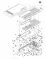
14. Parts
DJ
ExtE
NO.
1
2
3
I- 4
5
~
6
I7
8
9
10
GCi
GCi
GF°
PF
PS I
PG I
P GI
C Pl
DU I
L X·
11 PG I
12 G F
13 PT I
14 o ·r ,
L l 5 loT
16
17 MS
18 PT I
19 RA
20 PT I
21 G C,
22 L X ·
23 L F
24 TC,
25 G F
_26 L X ·
28 PC I
29 p
30 GF
31 L X ·
32 J KI
33 TL
34 p CI
35 TL.
1-101 L X ·
ocl
z
I-
I
I
[£]PW
NO.
-15-
14. Parts list & Guide
[I] Exteriors
NO.
1
2
3
4
5
6
7
8
9
10
11
12
13
14
15
16
17
18
19
20
21
22
23
24
25
26
28
29
30
31
32
33
34
35
101
PARTS CODE
GCASP1006ECZZ
GCABB1047EC03
GFTAA1287CCSA
PFiLWlOlOECZZ
PSLDP1026ECSA
PGUMM1031ECSA
PGUMM1030ECSB
CPWBN1079EC02
DUNT-1343ECZZ
LX-BZl 109CCZZ
PGUMS1549CCZZ
GFTAB1015ECZZ
PTPEH1038EC01
QTANZ1019ECZZ
_Q_TANZ1021ECZZ
_Q_CNTM1042CCZZ
MSLiP1031CC04
P TPEH 1 0 3 9 EC0 1
RALMB1030CCZZ
PTPEH1213CCZZ
GCABA1048EC01
LX-BZ1263CCZZ
LFiX-1190CCSF
TCAUK1242CCZZ
GFTAU1006ECSC
LX-BZ1038CCZZ
PCUSSlOlOECZZ
PZETL1046ECZZ
GFTAB1306CCZZ
LX-BZ1024ECZZ
JKNBZ1225CCZZ
TLABH1266ECZZ
PCU SS 1 0 1 0 EC Z Z
TLABH1267ECZZ
LX - NZ1020CCZZ
PRICE NEW
RANK MARK
AG
N
AL
N
AB
AD
N
AC
N
AK
N
AM
N
BX
N
AY
N
AA
AE
AB
N
N
AD
AB
N
AC
N
AA
AC
N
AB
N
AD
AB
AG
N
AA
N
AB
N
AA
AF
N
AA
AA
N
AA
N
AD
AA
N
AB
AC
N
AA
N
AC
N
AA
PART
DESCRIPTION
RANK
D
Hard case
TQI>_ cabinet
D
D
Connector lidJ!or l~n connecto!l_
D
Ac!)') filter
PRICE NEW
RANK MARK
AY
N
AB
AA
AB
N
AA
N
AA
AA
N
AG
AM
AB
N
AC
N
AC
AA
N
AB
N
AC
AB
N
AD
N
AD
N
AK
N
AF
AA
AA
AB
N
AA
N
AB
AB
AS
N
AX
AY
N
AE
BA
N
AC
N
AC
N
AC
BB
N
AA
AA
PART
RANK
E
c
Dis~l~mask
B
B
E
E
K~rubber B
KE!Y_rubber A
PWB unit
LCD unit
Screw:I2X4.5I
PWB card connector
Batte.!}'._ lid
Shield t~ A
Batte!'.Y_ terminal Ef1
Battery_ terminal-8_
Slide switch terminal
Slider for connector lid
Shield t~e B
BuzzerJ..EFB-S49C02PI
Adhesive t~ for buzzer
Bottom cabinet
Screw
Fixil!8._Qlate for card
Caution label
Card lid
Screw
Cushion
Insulation sheet for batte!'.Y_
Batte!Y_ cover
Screw
Slide switch knob
Batte.!}'._r~acernent label A
Cushion
Batte!'.Y_r~acement label B
Nut
c
c
D
c
c
c
c
c
c
B
c
D
c
c
c
D
c
c
c
D
c
c
D
c
D
c
:IA ttach to the !QI>_ cabine!i
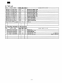
[£] PWB unit
NO.
1
2
3
4
5
6
7
8
9
10
11
12
13
14
15
16
17
18
19
20
21
22
23
24
25
26
27
28
29
30
31
32
33
34
35
36
37
PARTS CODE
DUNT-1343ECZZ
MSPRC1007ECZZ
MSPRC1277CCZZ
PGUMS1027ECZZ
PSPAPlOllECZZ
PSPAP1289CCZZ
PZETL1050ECZZ
QCNCWlOOlEClA
QCNCW1368CC1E
QTANZ1019ECZZ
QTANZ1021ECZZ
QTANZ1478CCSA
QTANZ1545CCZZ
QTANZ1557CCZZ
RC - CZD105ECZZ
RC-EZ107AEC1A
RCRM - 1003ECZZ
RH - DZlOOlECZZ
RTRNH 1 0 0 4 EC Z Z
RVR - Z2400QCZZ
VCCCTP1HH151J
VCCCTP1HH470J
VCEAJU1EW335M
VCKYTP1HB472K
VHDDAN202K / - l
VHEHZ9Cl// / - l
VHiHD61202 / - l
VHiHD61203 / - l
VHiLH5320XH - l
V H i MN 1 2 8 OQ/ - 1
VHiSC62015BOl
VHiTC4S66F/ - l
VHiTC4S81FTPR
VHiTC7S04FTPR
VHi6256LFlXSL
VRS-TP2BD102J
VRS - TP 2 BD104J
c
c
B
c
c
c
c
c
c
c
c
c
c
c
c
B
B
B
B
c
c
c
c
B
B
B
B
B
B
B
B
B
B
B
c
c
DESCRIPTION
LCD unit
Card cover ~ii!&.
Connector ~ing]for l~n connectod:
Rubber connector
Insulation ~cer
~cer for 1 !Qin connector
Insulation sheet
Connector]) !Qiri.[
Connector j) ~ri.[
Battert. terminal] [
Batteiy terminal 8
Power terminal
Terminal for memo!Y_ back l,lll_batte!Y. Ef1
Terminal for memo!Y_ back l,lll_batte!'.Y_ 8
Ca_Q!lcitorJ.!l!f_l
Ca...E!_acitorj_lOWV 10~
C!Y_sta((2.3MHtl:
Diode J.RB400DI
Converter transformer
Variable resistor:I20KO[
C'!.1!_acitor:i50WV 150PQ
C~acitor1_50WV 47Pfl
C~acitorJ..25WV 3.3.l!fJ.
C'!.1!_acitorJ..50WV 4700PQ
DiodeJ..DAN202KI
Zener diode{HZ9C l}
ICJ:HD61202J
ICJ:HD6120~
IC~H5320XH}
ICJ:MN128QQ}_
ICJ:SC62015B01[
ICJ..TC4S661}_
ICJ..TC4S81FTPR_l
ICJ..TC7S04FTPRI
ICJ:6256LF1XSI}
Resistor:Il/8W l.OKO ±5]61
ResistorJ..l/8W lOOKO +5%)
- 16-
-
PC-E500
2
3
4
5
8
15
19 '20
33
25
29 22 35
-17-
-
PC-E500
[2J PWB unit
NO.
PARTS CODE
38 VRS-TP2B0184J
39 VRS-TP2B0243J
40 VRS-TP2B0392G
41 VRS-TP2B0393G
42 VRS-TP2B04R7J
43 VRS-TP2B0472J
44 VRS-TP2B0563J
45 VRS-TP2B0681J
46 VRS-TP2B0822J
47 VSOTA114Y~-l
48 VSOTA144EK/-l
49 VSOTC144EK/-l
50 VS2SC2412K/-l
51 VS2SC2412KS-l
(Unifi:
901 C PW B N 1 0 7 9 EC OJ.:.::±:
PRICE NEW
RANK MARK
AA
AA
AA
N
AA
AA
AA
AA
AA
AA
AC
AC
AC
AB
AB
BX
N
PART
RANK
c
c
c
c
c
c
c
c
c
DESCRIPTION
B
B
B
B
B
ResistorJ..l/BW 180KO ±5%)
ResistorJ..l/BW 24KO + 5%1
ResistorJ..l/BW 3.9KO +2_%1
ResistorJ_l/BW 39KO +2_%1
ResistorJ_l/BW 4.70 +5%)
Resistor_(._l/BW 4.7KO +5%)
Resistorll/BW 56KO ±5%)
ResistorJ_l/BW 6800 +s}il
ResistorJ_l/BW 8.2KO +sfil
TransistorJ_OTAl 14YKJ.
Transistor_(_OTA l 44E~
Transistor_(_OTC l 44E~
Transistorl2SC24 l 2KJ.
Transistorl2SC24 l 2K~
E
PWB unit
CT] Packing material & Accessories
NO.
PARTS CODE
SPAKC0463ECZZ
SPAKA0381ECZZ
SSAKA0006UCZZ
SSAKA5003CCZZ
TiNSG1188ECZZ
5
T i NSE1189ECZZ
1
2
3
4
PRICE NEW
RANK MARK
AK
N
AE
N
AA
AA
AT
N
AZ
N
PART
RANK
0
Packi!!.8_ case
0
Packi!!.8_ cushion for set
0
ViQi'.) b~50X6Ql
0
ViQi'.) b!!.&J.140 X 260nn}
0
Instruction book
0
Instruction book...1.E G Q
-18-
DESCRIPTION
:Itor Germaritl
for Germa'!tl
_(exc~
-
PC-E500
SHARP
COPYRIGHT
©
1989 BY SHARP CORPORATION
All rights reserved.
Printed in Japan.
No part of this publication may be reproduced,
stored in a retrieval system, or transmitted,
in any form or by any means,
electronic, mechanical , photocopying, recording, or otherwise,
without prior written permission of the publisher.
SHARP CORPORATION
lnformatiOn Systems Group
Quality & Reliability Control Center
Yamatokoriyarna, Nara 639-11, Japan
1989 August Printed in Japan <S>