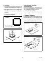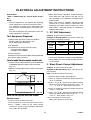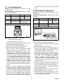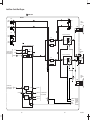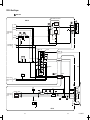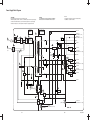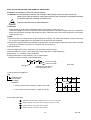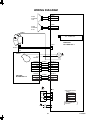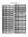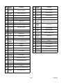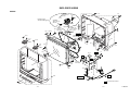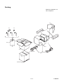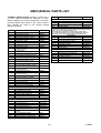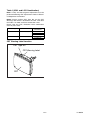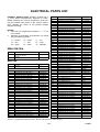
1
SERVICE MANUAL
20" COLOR TELEVISION
TV-2000A MK12
IMPORTANT SAFETY NOTICE
Proper service and repair is important to the safe, reliable operation of all
Funai Equipment. The service procedures recommended by Funai and described in this service manual are effective methods of performing service
operations. Some of these service special tools should be used when and
as recommended.
It is important to note that this service manual contains various CAUTIONS
and NOTICES which should be carefully read in order to minimize the risk
of personal injury to service personnel. The possibility exists that improper
service methods may damage the equipment. It also is important to understand that these CAUTIONS and NOTICES ARE NOT EXHAUSTIVE. Funai
could not possibly know, evaluate and advice the service trade of all conceivable ways in which service might be done or of the possible hazardous
consequences of each way. Consequently, Funai has not undertaken any
such broad evaluation. Accordingly, a servicer who uses a service procedure or tool which is not recommended by Funai must first use all precautions thoroughly so that neither his safety nor the safe operation of the
equipment will be jeopardized by the service method selected.
TABLE OF CONTENTS
Specifications...........................................................1-1
Important Safety Precautions...................................2-1
Standard Notes for Servicing ...................................3-1
Disassembly Instructions .........................................4-1
Electrical Adjustment Instructions ............................5-1
Block Diagram..........................................................6-1
Schematic Diagram / CBA’s and Test Points ..........7-1
Schematic Diagram .................................................7-3
CBA Views and Test Points ................................... 7-11
Wave Forms ............................................................ 8-1
Wiring Diagram........................................................ 9-1
IC Pin Fuction........................................................ 10-1
Cabinet Exploded View ..........................................11-1
Packing Exploded View..........................................11-3
Mechanical Parts List ............................................ 12-1
Electrical Parts List................................................ 13-1
SPECIFICATIONS
< TUNER>
ANT. Input ------------------------- 75ohm Unbal., F type
Reference Level ----------------- 20Vp-p (CRT Green Cathode)
Test Input Signal ----------------- 400Hz 30% modulation
Description
Condition
Unit
Nominal
Limit
1. Intermediate Freq.
Picture
Sound(B/G)
(D/K)
MHz
MHz
MHz
38.0
32.5
31.5
—
—
2. Peak Picture Sens
VHF
CATV
UHF
dBµV
dBµV
dBµV
15
15
15
30
30
40
3. AFT Pull In Range
(10mV input)
—
MHz
± 2.3
± 0.7
Condition
Unit
Nominal
Limit
Horizontal
KHz
Hz
Hz
15.625(PAL)
15.750(NTSC)
50
60
—
—
Horizontal
Vertical
%
%
—
—
± 15
± 10
3. Over Scan
—
%
10
—
4. High Voltage
—
KV
26
—
Condition
Unit
Nominal
Limit
Center
Side
Corner
mm
mm
mm
—
—
—
0.4
1.5
2.1
APL 100%
Ft-L
40
25
—
°K
8000°K-10MPCD
—
Horizontal
Vertical
Line
Line
350
400
—
—
< DEFLECTION>
Description
1. Deflection Freq.
Vertical(PAL)
(NTSC)
2. Linearity
< VIDEO & CHROMA>
Description
1. Misconvergence
2. Brightness
3. Color Temperature
4. Resolution
<AUDIO>
All items are measured across 8Ω load at speaker output terminal.
Description
1. Audio Output Power
2. Audio Distortion (w/LPF)
3. Audio Freq. Response
Condition
Unit
Nominal
Limit
10% THD
W
3
2.7
500mW
%
2
5
−3dB
Hz
100~10K
—
Note:
Nominal specifications represent the design specifications. All units should be able to approximate
these. Some will exceed and some may drop slightly below these specifications. Limit specifications
represent the absolute worst condition that still might be considered acceptable. In no case should
a unit fail to meet limit specifications.
1-1
L1700SP
IMPORTANT SAFETY PRECAUTIONS
Prior to shipment from the factory, our products are strictly inspected for recognized product safety and electrical
codes of the countries in which they are to be sold. However, in order to maintain such compliance, it is equally
important to implement the following precautions when a set is being serviced.
current tester or a metering system that complies
with American National Standards Institute (ANSI)
C101.1 Leakage Current for Appliances and Underwriters Laboratories (UL) 1410, (50.7). With the
instrument AC switch first in the on position and then
in the off position, measure from a known earth
ground (metal water pipe, conduit, etc.) to all exposed metal parts of the instrument (antennas, handle brackets, metal cabinet, screw heads, metallic
overlays, control shafts, etc.), especially any exposed metal parts that offer an electrical return path
to the chassis. Any current measured must not
exceed 0.5 milli-ampere. Reverse the instrument
power cord plug in the outlet and repeat the test.
Safety Precautions for TV Circuit
1. Before returning an instrument to the customer, always make a safety check of the entire
instrument, including, but not limited to, the following
items:
a. Be sure that no built-in protective devices are defective and have been defeated during servicing. (1)
Protective shields are provided on this chassis to
protect both the technician and the customer. Correctly replace all missing protective shields, including any removed for servicing convenience. (2)
When reinstalling the chassis and/or other assembly
in the cabinet, be sure to put back in place all
protective devices, including but not limited to, nonmetallic control knobs, insulating fishpapers, adjustment and compartment covers/shields, and isolation resistor/capacitor networks. Do not operate
READING SHOULD
NOT BE ABOVE 0.5 mA
this instrument or permit it to be operated
without all protective devices correctly installed and functioning. Servicers who defeat safety features or fail to perform safety
checks may be liable for any resulting damage.
DEVICE
BEING
TESTED
LEAKAGE
CURRENT
TESTER
_
+
TEST ALL EXPOSED
METAL SURFACES
b. Be sure that there are no cabinet openings through
which an adult or child might be able to insert their
fingers and contact a hazardous voltage. Such
openings include, but are not limited to, (1) spacing
between the picture tube and the cabinet mask, (2)
excessively wide cabinet ventilation slots, and (3) an
improperly fitted and/or incorrectly secured cabinet
back cover.
ALSO TEST WITH
PLUG REVERSED
USING AC
ADAPTER PLUG
AS REQUIRED
EARTH
GROUND
c. Antenna Cold Check - With the instrument AC
ANY MEASUREMENTS NOT WITHIN THE LIMITS
SPECIFIED HEREIN INDICATE A POTENTIAL
SHOCK HAZARD THAT MUST BE ELIMINATED
BEFORE RETURNING THE INSTRUMENT TO
THE CUSTOMER OR BEFORE CONNECTING
THE ANTENNA OR ACCESSORIES.
plug removed from any AC source, connect an
electrical jumper across the two AC plug prongs.
Place the instrument AC switch in the on position.
Connect one lead of an ohmmeter to the AC plug
prongs tied together and touch the other ohmmeter
lead in turn to each tuner antenna input exposed
terminal screw and, if applicable, to the coaxial
connector. If the measured resistance is less than
1.0 megohm or greater than 5.2 megohm, an abnormality exists that must be corrected before the instrument is returned to the customer. Repeat this
test with the instrument AC switch in the off position.
e. X-Radiation and High Voltage Limits - Because the picture tube is the primary potential
source of X-radiation in solid-state TV receivers, it
is specially constructed to prohibit X-radiation emissions. For continued X-radiation protection, the replacement picture tube must be the same type as
the original. Also, because the picture tube shields
and mounting hardware perform an X-radiation protection function, they must be correctly in place.
High voltage must be measured each time servicing
d. Leakage Current Hot Check - With the instrument completely reassembled, plug the AC line cord
directly into a 120V AC outlet. (Do not use an isolation transformer during this test.) Use a leakage
2-1
SFTYP_01
ground. If a voltage reading in excess of 1.0V is
obtained, remove and reinsert the AC power plug in
the opposite polarity and again measure the voltage
potential between the chassis and a known earth
ground.
is performed that involves B+, horizontal deflection
or high voltage. Correct operation of the X-radiation
protection circuits also must be reconfirmed each
time they are serviced. (X-radiation protection circuits also may be called "horizontal disable" or "hold
down.") Read and apply the high voltage limits and,
if the chassis is so equipped, the X-radiation protection circuit specifications given on instrument labels
and in the Product Safety & X-Radiation Warning
note on the service data chassis schematic. High
voltage is maintained within specified limits by close
tolerance safety-related components/adjustments
in the high-voltage circuit. If high voltage exceeds
specified limits, check each component specified on
the chassis schematic and take corrective action.
b. Some TV receiver chassis normally have 85V
AC(RMS) between chassis and earth ground regardless of the AC plug polarity. This chassis can be
safety-serviced only with an isolation transformer
inserted in the power line between the receiver and
the AC power source, for both personnel and test
equipment protection.
c. Some TV receiver chassis have a secondary ground
notes on or inside the receiver cabinet, on the receiver chassis, or on the picture tube.
system in addition to the main chassis ground. This
secondary ground system is not isolated from the
AC power line. The two ground systems are electrically separated by insulation material that must not
be defeated or altered.
3. Design Alteration Warning - Do not alter or add
6. Observe original lead dress. Take extra care to
2. Read and comply with all caution and safety-related
to the mechanical or electrical design of this TV
receiver. Design alterations and additions, including, but not limited to circuit modifications and the
addition of items such as auxiliary audio and/or
video output connections, might alter the safety
characteristics of this receiver and create a hazard
to the user. Any design alterations or additions will
void the manufacturer’s warranty and may make
you, the servicer, responsible for personal injury or
property damage resulting therefrom.
assure correct lead dress in the following areas: a.
near sharp edges, b. near thermally hot parts-be
sure that leads and components do not touch thermally hot parts, c. the AC supply, d. high voltage,
and e. antenna wiring. Always inspect in all areas
for pinched, out of place, or frayed wiring. Check AC
power cord for damage.
7. Components, parts, and/or wiring that appear to
have overheated or are otherwise damaged should
be replaced with components, parts, or wiring that
meet original specifications. Additionally, determine
the cause of overheating and/or damage and, if
necessary, take corrective action to remove any
potential safety hazard.
4. Picture Tube Implosion Protection Warning
- The picture tube in this receiver employs integral
implosion protection. For continued implosion protection, replace the picture tube only with one of the
same type number. Do not remove, install, or otherwise handle the picture tube in any manner without
first putting on shatterproof goggles equipped with
side shields. People not so equipped must be kept
safely away while picture tubes are handled. Keep
the picture tube away from your body. Do not handle
the picture tube by its neck. Some "in-line" picture
tubes are equipped with a permanently attached
deflection yoke; because of potential hazard, do not
try to remove such "permanently attached" yokes
from the picture tube.
8. Product Safety Notice - Some electrical and
mechanical parts have special safety-related characteristics which are often not evident from visual
inspection, nor can the protection they give necessarily be obtained by replacing them with components rated for higher voltage, wattage, etc.. Parts
that have special safety characteristics are identified
by a (
) on schematics and in parts lists. Use of
a substitute replacement that does not have the
same safety characteristics as the recommended
replacement part might create shock, fire, and/or
other hazards. The product’s safety is under review
continuously and new instructions are issued whenever appropriate. Prior to shipment from the factory,
our products are strictly inspected to confirm they
comply with the recognized product safety and electrical codes of the countries in which they are to be
sold. However, in order to maintain such compliance, it is equally important to implement the following precautions when a set is being serviced.
!
5. Hot Chassis Warning a. Some TV receiver chassis are electrically connected directly to one conductor of the AC power
cord and may be safety-serviced without an isolation
transformer only if the AC power plug is inserted so
that the chassis is connected to the ground side of
the AC power source. To confirm that the AC power
plug is inserted correctly, with an AC voltmeter,
measure between the chassis and a known earth
2-2
SFTYP_01
3) Align the lengths of the wires to be connected. Insert
the wires fully into the connector.
Precautions during Servicing
A. Parts identified by the (
safety.
! ) symbol are critical for
4) Use the crimping tool to crimp the metal sleeve at
the center position. Be sure to crimp fully to the
complete closure of the tool.
Replace only with part number specified.
B. In addition to safety, other parts and assemblies are
L. When connecting or disconnecting the internal con-
specified for conformance with regulations applying
to spurious radiation. These must also be replaced
only with specified replacements.
nectors, first, disconnect the AC plug from the AC
supply outlet.
Examples: RF converters, RF cables, noise blocking capacitors, and noise blocking filters, etc.
C. Use specified internal wiring. Note especially:
1) Wires covered with PVC tubing
2) Double insulated wires
3) High voltage leads
D. Use specified insulating materials for hazardous live
parts. Note especially:
1) Insulation Tape
2) PVC tubing
3) Spacers
4) Insulators for transistors.
E. When replacing AC primary side components
(transformers, power cord, etc.), wrap ends of wires
securely about the terminals before soldering.
F. Observe that the wires do not contact heat producing parts (heatsinks, oxide metal film resistors, fusible resistors, etc.)
G. Check that replaced wires do not contact sharp
edged or pointed parts.
H. When a power cord has been replaced, check that
5~6 kg of force in any direction will not loosen it.
I. Also check areas surrounding repaired locations.
J. Use care that foreign objects (screws, solder droplets, etc.) do not remain inside the set.
K. Crimp type wire connector
The power transformer uses crimp type connectors
which connect the power cord and the primary side
of the transformer. When replacing the transformer,
follow these steps carefully and precisely to prevent
shock hazards.
Replacement procedure
1) Remove the old connector by cutting the wires at a
point close to the connector.
Important: Do not re-use a connector (discard it).
2) Strip about 15 mm of the insulation from the ends of
the wires. If the wires are stranded, twist the strands
to avoid frayed conductors.
2-3
SFTYP_01
Safety Check after Servicing
Chassis or Secondary Conductor
Examine the area surrounding the repaired location for
damage or deterioration. Observe that screws, parts
and wires have been returned to original positions.
Afterwards, perform the following tests and confirm the
specified values in order to verify compliance with safety
standards.
Primary Circuit Terminals
d'
d
1. Clearance Distance
When replacing primary circuit components, confirm
specified clearance distance (d) and (d’) between soldered terminals, and between terminals and surrounding metallic parts. (See Fig. 1)
Table 1 : Ratings for selected area
AC Line Voltage
Clearance Distance (d) (d’)
110 to 240 V
≥ 3mm(d)
≥ 6 mm(d’)
Fig. 1
Note: This table is unofficial and for reference only. Be
sure to confirm the precise values.
Exposed Accessible Part
2. Leakage Current Test
Z
Confirm the specified (or lower) leakage current between B (earth ground, power cord plug prongs) and
externally exposed accessible parts (RF terminals, antenna terminals, video and audio input and output terminals, microphone jacks, earphone jacks, etc.) is lower
than or equal to the specified value in the table below.
AC Voltmeter
(High Impedance)
1.5kΩ
0.15µF
Measuring Method : (Power ON)
Insert load Z between B (earth ground, power cord plug
prongs) and exposed accessible parts. Use an AC
voltmeter to measure across both terminals of load Z.
See Fig. 2 and following table.
B
Earth Ground
Power Cord Plug Prongs
Fig. 2
Table 2 : Leakage current ratings for selected areas
AC Line Voltage
110 to 240 V
Load Z
Leakage Current (i)
One side of power cord plug
prongs (B) to:
2kΩ RES.
Connected in
parallel
i≤0.7mA AC Peak
i≤2mA DC
RF or
Antenna terminals
50kΩ RES.
Connected in
parallel
i≤0.7mA AC Peak
i≤2mA DC
A/V Input, Output
Note: This table is unofficial and for reference only. Be sure to confirm the precise values.
2-4
SFTYP_01
STANDARD NOTES FOR SERVICING
(2) Remove the flat pack-IC with tweezers while applying the hot air.
Circuit Board Indications
a. The output pin of the 3 pin Regulator ICs is indicated
as shown.
Top View
Out
(3) Bottom of the flat pack-IC is fixed with glue to the
CBA; when removing entire flat pack-IC, first apply
soldering iron to center of the flat pack-IC and heat
up. Then remove (glue will be melted). (Fig. S-1-6)
Bottom View
In
Input
(4) Release the flat pack-IC from the CBA using tweezers. (Fig. S-1-6)
Caution:
1. Do not supply hot air to the chip parts around the flat
pack-IC for over 6 seconds because damage to the
chip parts may occur. Put masking tape around the
flat pack-IC to protect other parts from damage.
(Fig. S-1-2)
b. For other ICs, pin 1 and every fifth pin are indicated
as shown.
5
2. The flat pack-IC on the CBA is affixed with glue, so
be careful not to break or damage the foil of each
pin or the solder lands under the IC when removing
it.
Pin 1
10
Hot-air
Flat Pack-IC
Desoldering
Machine
c. The 1st pin of every male connector is indicated as
shown.
CBA
Pin 1
Masking
Tape
How to Remove / Install Flat Pack-IC
Tweezers
1. Removal
Flat Pack-IC
Fig. S-1-2
With Hot-Air Flat Pack-IC Desoldering Machine:
(1) Prepare the hot-air flat pack-IC desoldering machine, then apply hot air to the Flat Pack-IC (about
5 to 6 seconds). (Fig. S-1-1)
Fig. S-1-1
3-1
SFTY_08
With Soldering Iron:
soldering iron to center of the flat pack-IC and heat
up. Then remove (glue will be melted). (Fig. S-1-6)
(1) Using desoldering braid, remove the solder from all
pins of the flat pack-IC. When you use solder flux
which is applied to all pins of the flat pack-IC, you
can remove it easily. (Fig. S-1-3)
Flat Pack-IC
(5) Release the flat pack-IC from the CBA using tweezers. (Fig. S-1-6)
Note:
When using a soldering iron, care must be taken to
ensure that the flat pack-IC is not being held by glue.
When the flat pack-IC is removed from the CBA,
handle it gently because it may be damaged if force
is applied.
Desoldering Braid
Hot Air Blower
Soldering Iron
Fig. S-1-3
or
(2) Lift each lead of the flat pack-IC upward one by one,
using a sharp pin or wire to which solder will not
adhere (iron wire). When heating the pins, use a fine
tip soldering iron or a hot air desoldering machine.
(Fig. S-1-4)
Iron Wire
Soldering Iron
To Solid
Mounting Point
Fig. S-1-5
Sharp
Pin
CBA
Fine Tip
Soldering Iron
Fine Tip
Soldeing Iron
Fig. S-1-4
(3) Bottom of the flat pack-IC is fixed with glue to the
CBA; when removing entire flat pack-IC, first apply
soldering iron to center of the flat pack-IC and heat
up. Then remove (glue will be melted). (Fig. S-1-6)
Flat Pack-IC
(4) Release the flat pack-IC from the CBA using tweezers. (Fig. S-1-6)
Tweezers
With Iron Wire:
Fig. S-1-6
(1) Using desoldering braid, remove the solder from all
pins of the flat pack-IC. When you use solder flux
which is applied to all pins of the flat pack-IC, you
can remove it easily. (Fig. S-1-3)
(2) Affix the wire to a workbench or solid mounting point,
as shown in Fig. S-1-5.
(3) While heating the pins using a fine tip soldering iron
or hot air blower, pull up the wire as the solder melts
so as to lift the IC leads from the CBA contact pads
as shown in Fig. S-1-5.
(4) Bottom of the flat pack-IC is fixed with glue to the
CBA; when removing entire flat pack-IC, first apply
3-2
SFTY_08
2. Installation
Instructions for Handling
Semiconductors
(1) Using desoldering braid, remove the solder from the
foil of each pin of the flat pack-IC on the CBA so you
can install a replacement flat pack-IC more easily.
Electrostatic breakdown of the semiconductors may
occur due to a potential difference caused by electrostatic charge during unpacking or repair work.
(2) The " ● " mark on the flat pack-IC indicates pin 1.
(See Fig. S-1-7.) Be sure this mark matches the 1
on the PCB when positioning for installation. Then
pre- solder the four corners of the flat pack-IC. (See
Fig. S-1-8.)
1. Ground for Human Body
Be sure to wear a grounding band (1MΩ) that is properly
grounded to remove any static electricity that may be
charged on the body.
(3) Solder all pins of the flat pack-IC. Be sure that none
of the pins have solder bridges.
2. Ground for Workbench
Be sure to place a conductive sheet or copper plate with
proper grounding (1MΩ) on the workbench or other
surface, where the semiconductors are to be placed.
Because the static electricity charge on clothing will not
escape through the body grounding band, be careful to
avoid contacting semiconductors with your clothing.
Example :
< Incorrect >
Pin 1 of the Flat Pack-IC
is indicated by a " ● " mark.
Fig. S-1-7
CBA
Presolder
< Correct >
Grounding Band
Flat Pack-IC
CBA
Fig. S-1-8
1MΩ
CBA
1MΩ
Conductive Sheet or
Copper Plate
3-3
SFTY_08
CABINET DISASSEMBLY INSTRUCTIONS
Note :
1. Disassembly Flowchart
➀. Order of steps in procedure. When reassembling,
This flowchart indicates the disassembly steps for the
cabinet parts, and the CBA in order to gain access to
item(s) to be serviced. When reassembling, follow the
steps in reverse order. Bend, route and dress the cables
as they were.
follow the steps in reverse order.
These numbers are also used as the Identification
(location) No. of parts in figures.
➁. Parts to be removed or installed.
➂. Fig. No. showing procedure of part location
➃. Identification of part to be removed, unhooked, un-
Caution !
When removing the CRT, be sure to discharge the
Anode Lead of the CRT with the CRT Ground Wire
before removing the Anode Cap.
locked, released,
desoldered.
unplugged,
unclamped,
or
S=Screw, P=Spring, L=Locking Tab, CN=Connector, *=Unhook, Unlock, Release, Unplug, or
Desolder
[1] Rear Cabinet
2(S-2) = two Screws (S-2)
➄. Refer to the following "Reference Notes in the
[2] CRT CBA
Table."
Reference Notes in the Table
[3] Main CBA
1. Removal of the Rear Cabinet. Remove screws
5(S-1) and (S-3) then slide the Rear Cabinet backward.
[4] CRT
2. Removal of the CRT CBA. Disconnect CN501 then
pull the CRT CBA backward.
2. Disassembly Method
3. Removal of the Main CBA. Disconnect CN571 on
the Main CBA then slide the Main CBA backward.
Removal
Step/
Loc. No.
[1]
Part
Rear
Cabinet
Fig.
No.
1,2
Remove/*unlock/
release/unplug/
unclamp/desolder
5(S-1), 1(S-3),
1(S-4)
Caution !
Note
1
[2]
CRT CBA
4,5
CN501
2
[3]
Main CBA
3,5
CN571
3
[4]
CRT
4
4(S-2), Anode Cap
Discharge the Anode Lead of the CRT with the CRT
Ground Wire before removing the Anode Cap.
4. Removal of the CRT. Remove screws 4(S-2) and
Anode Cap. then slide the CRT backward.
4
↓
↓
↓
↓
↓
➀
➁
➂
➃
➄
4-1
L1700DC
S-1
[3]Main CBA
ANT.IN
R
AUDIO
L
OUT
R
L(MONO)
VIDEO
IN
Front Cabinet
S-4
S-3
Control Plate
S-1
[1] Rear Cabinet
Fig. 1
Fig. 3
S-1
S-1
Degauss Holder
S-2
Anode Cap
[2]CRT CBA
Degaussing Coil
CRT Ground Wire
S-2
S-2
S-1
S-1
S-1
[4]CRT
[1]Rear Cabinet
S-2
Front Cabinet
Control Plate
Front Cabinet
Control Plate
Fig. 4
Fig. 2
4-2
L1700DC
TV Cable Wiring Diagram
SP801
SP802
L691 DEGAUSSING COIL
CLN801
CLN802
MAIN CBA
CN802
CN801
CN691
TU1
TUNER
FLYBACK TRANSFORMER
T571
CN571
AC601
AC CORD
WH301A
WH501A
FOCUS
JK501
SCREEN
WH301B
WH501B
ANODE
CN501
TO CRT GROUND
4-3
Fig. 5
L1700DC
ELECTRICAL ADJUSTMENT INSTRUCTIONS
General Note:
"CBA" is abbreviation for "Circuit Board Assembly".
4. When CPU version is 054-0.13: Check the display
on the lower left is "00" and if it is not "00", set it at
"00" according to "3-1 FRENCH, ACCESS CODE,
VIDEO TONE".
NOTE:
When CPU version is 200-0.07: Confirm that the
character of U ( U.S.A. model ) is indicated on the
bottom left of the CRT. If the character of C ( CANADA model ) is indicated, perform "3-1 Setting for
FRENCH data Values".
Electrical adjustments are required after replacing
circuit components and certain mechanical parts.
It is important to perform these adjustments only
after all repairs and replacements have been completed.
Also, do not attempt these adjustments unless the
proper equipment is available.
1. DC 105V Adjustment
Purpose: To obtain correct operation.
Test Equipment Required
Symptom of Misadjustment: The picture is dark and
the unit does not operate correctly.
1. NTSC Pattern Generator (Color Bar W/White
Window, Red Color, Dot Pattern, Gray
Scale, Monoscope, Multi-Burst)
2. DC Voltmeter
3. Oscilloscope: Dual-trace with 10:1 probe,
V-Range: 0.001~50V/Div,
F-Range: DC~AC-60MHz
4. Plastic Tip Driver
Test Point
Adj. Point
Mode
Input
TP601
TP300
(GND)
VR661
---
---
Tape
M. EQ.
Spec.
---
DC Voltmeter
+114±1.0V DC.
Note: TP601, TP300(GND), VR661 --- Main CBA
5. Remote control unit:Part No. N0121UD or N0134UD
1. Connect DC Volt Meter to TP601 and TP300(GND).
6. DC power supply 13.2V/5A
2. Adjust VR661 so that the voltage of TP601 becomes
+113±1.0V DC.
How to make Service remote control unit:
1. Prepare normal remote control unit. (Part No. N0121UD
or N0134UD) Remove 3 Screws from the back lid.
(Fig. 1-1)
2. Black Strech Control Adjustment
Purpose: To show the fine black color.
2. Added J1 (Jumper Wire) to the remote control CBA.
(Fig. 1-2)
Symptom of Misadjustment: Black color will not appear correctly.
SCREWS
Note: Use Service remote control unit.
1. Enter the Service mode. (See page 5-1)
2. Press " 6 " button on the Service remote control unit.
" B-S " is indicated.
Fig. 1-1
3. Press " CH ▲ / ▼ " buttons on the Service remote
control unit so that display will change " OFF ", " 0
", " 1 ", " 2 " and " 3 ". Then choose " B-S OFF ".
J1
REMOTE CONTROL UNIT
REMOTE CONTROL CBA
4. Press " 6 " button on the Service remote control unit.
" B-S*2 " is indicated.
5. Press " CH ▲ / ▼ " buttons on the Service remote
control unit so that display will change " 0", " 1 ". " 2
" and " 3 ". Then choose " B-S*2 0".
Fig. 1-2
How to set up the service mode:
6. Turn the power off and on again.
(Main power button on the TV unit.)
Service mode:
1. Use the service remote control unit.
2. Turn the power on. (Use main power on the TV unit.)
3. Press " SLEEP " button on the service remote
control unit. Version of micro computer will display
on the CRT. (Ex: 056-0.07)
5-1
L1700EA
2. Press " CH ▲ / ▼ " buttons on the Service remote
control unit. Then choose VHFL/VHFH/UHF.
3-1. Setting for 7F, H/L STEP, TV
DELAY, SOUND SYS, BAND
SELECT, VIF FREQUENCY
and RF AMP data Values
VIF FREQUENCY
1. Press " VOL ▼ " button on the Service remote
control unit. Then select VIF FREQ display.
General
2. Press " CH ▲ / ▼ " buttons on the Service remote
control unit. Then choose VIF FREQ=38.
1. Enter the Service mode. (See page 5-1)
2. Press " VOL ▼ " button on the Service remote
control unit. Display changes "C/D/SCM B-L",
"VCO", "7F", "H/L STEP", "TV DELAY", "SOUND
SYSTEM", "VHFL/VHFH/UHF", "VIF FREQ"and
"RF AMP" cyclically when " VOL ▼ " button is
pressed.
RF AMP
1. Press " VOL ▼ " button on the Service remote
control unit. Then select RF AMP display.
2. Press " CH ▲ / ▼ " buttons on the Service remote
control unit. Then choose RF AMP=OFF.
7F
1. Press " VOL ▼ " button on the Service remote
control unit. Then select 7F display.
Note: C/D and VCO data values are no need to adjust
at this moment.
2. Press " CH ▲ / ▼ " buttons on the Service remote
control unit. Then choose 7F=FF.
3-2. Setting for CONTRAST,
COLOUR AND TINT
data Values
H/L STEP
1. Press " VOL ▼ " button on the Service remote
control unit. Then select H/L STEP display.
1. Enter the Service mode. (See page 5-1)
2. Press "1" button, you can select H-STEP(R).
2. Press " PICTURE SELECT " button on the Service
remote control unit. Display changes " BRIGHT ", "
CONTRAST ", " COLOUR ", " TINT " cyclically when
" PICTURE SELECT " button is pressed.
Press "2" button, you can select H-STEP(B).
Press "3" button, you can select L-STEP(R).
Press "4" button, you can select L-STEP(B).
Press " CH ▲ / ▼ " buttons on the Service remote
control unit so that the value of :
Press " CH ▲ / ▼ " button on the Service remote
control unit. Then choose:
CONTRAST becomes 84
H-STEP(R)=2
COLOUR becomes 52
H-STEP(B)=12
TINT becomes 60
L-STEP(R)=2
Note: BRIGHTdata value is no need to adjust at this
moment.
L-STEP(B)=8
TV DELAY
4. H fo Adjustment
1. Press " VOL ▼ " button on the Service remote
control unit. Then select TV DELAY display.
Purpose: To get correct horizontal frequency.
2. Press "1" button, you can select PAL DELAY.
Symptom of Misadjustment: . If H f0 adjustment is in
correct, sqew distortion will appear on the screen.
Press "2" button, you can select SECAM DELAY.
Press " CH ▲ / ▼ " button on the Service remote
control unit. Then choose:
PAL DELAY=2
SECAM DELAY=7
SOUND SYS
1. Press " VOL ▼ " button on the Service remote
control unit. Then select SOUND SYS display.
Test Point
Adj. Point
Mode
Input
TP302
CH ▲ / ▼ button
["H-ADJ"] MODE
Tape
M. EQ.
Spec.
----
Frequency
Counter
15.625 kHz±150Hz
----
Note: TP302 --- Main CBA
2. Press " CH ▲ / ▼ " buttons on the Service remote
control unit. Then choose SOUND SYS=OFF.
Use Service remote control unit.
1. Connect Frequency Counter to TP302 and ground.
BAND SELECT
2. Set the unit to the VIDEO mode which is located
before CH2 and no input is necessary. Enter the
Service mode. (See Page 5-1)
1. Press " VOL ▼ " button on the Service remote
control unit. Then select VHFL/VHFH/UHF ,
VHFL/VHFH, VHFH/UHF or UHF display.
5-2
L1700EA
2. Receive the Color Bar signal for channel 4
(62.25MHz). (RF Input Level: 60dBµV)
3. Operate the unit for at least 20 minutes.
4. Press "2" button on the Service remote control unit
and select H-ADJ Mode. (By pressing "2" button the
display will change from TV AGC to H-ADJ)
3. Press " CH ▲ / ▼ " buttons so that the voltage of
TP301 becomes +2.2±0.1V DC.
5. Press " CH ▲ / ▼ " button on the Service remote
control unit so that the display will change " 0 " ~ " 7 ".
At this moment, Choose display one of them from
" 0 " ~ " 7 " when the Frequency Counter shows 15.625
kHz±150Hz or closer.
4. Turn the Power off and on again. (Main power button
on the TV unit.)
7. Black Level Adjustment
Purpose: Set Sub-bright Level
6. Turn the power off and on again. (Main Power button
on the TV unit.)
Symptom of Misadjustment: If Sub-brightness is incorrect, Proper brightness can not be obtained by adjusting the Bright ness Control.
5. VCO Adjustment
Note: TP502, TP501 (GND) --- CRT CBA
Purpose: To operate VCO correctly.
1. Enter the Service mode. (See page 5-1).
Symptom of Misadjustment: VCO does not work correctly and/or synchronization is faulty.
Test Point
Adj. Point
Mode
---
---
Tape
M. EQ.
Spec.
---
---
---
2. Press " MENU " button on the Service remote control
unit and select " BRT "mode. (Display changes "
BRT ", " CNT ", " CLR " and " TNT "cyclically when
MENU button is pressed).
Input
No signal
3. Press " CH ▲ / ▼ " buttons on the Service remote
control unit so that the value of " BRT " becomes
128.
4. Turn the power off and on again. (Main power button
on the TV unit.)
Note: Use service remote control unit.
1. Disconnect the RF input and set the unit to Channel 4.
2. Enter the Service mode. (See Page 5-1)
8. C-Trap Adjustment
3. Press " 3 " button on the Service remote control unit.
The Auto VCO adjustment is started.
Purpose: To get minimum leakage of the color signal carrier.
Symptom of Misadjustment: If C- Trap Adjustment is
incorrect, stripes will appears on the screen.
4. If the display color is changed from red to green, This
adjustment is done.
5. Turn the Power off and on again. (Main power button
on the TV unit.)
6. AGC Adjustment
Purpose: Set AGC (Auto Gain Control) Level.
Symptom of Misadjustment: AGC does not synchronize correctly when RF input level is too weak and
picture distortion may occur if it is too strong.
Test
Point
Adj. Point
Mode
Input
RF
Color Bar
62.25MHz
60dBµV
Test Point
Adj. Point
Mode
Input
TP502
(Blue)
TP501
(GND)
CH ▲ / ▼ buttons
RF
Color Bar
Tape
M. EQ.
Spec.
----
Oscilloscope
----
Note: TP502, TP501 --- CRT CBA
Use Service remote control unit.
1. Connect Oscilloscope to TP502 and TP501 (GND).
2. Enter the Service mode. (See Page 5-1) Receive
color bar signal from RF Input.
TP301
CH ▲ / ▼ buttons
Tape
M. EQ.
Spec.
---
Pattern Generator
DC Volt Meter
3. Press " 0 " button on the Service remote control unit
and select C-TRP Mode.
+2.2±0.1VDC
4. Press " CH ▲ / ▼ " buttons on the Service remote
control unit so that the display will change " 0 ", " 1
", " 2 " and " 3 ". Choose display " 0 ", " 1 ", " 2 " or
" 3 " when B-Out (3.58MHz) value becomes
minimun on the oscilloscope reading.
Notes: TP301 --- Main CBA
Use Service remote control unit.
1. Enter the Service mode. (See Page 5-1) Then
5. Turn the power off and on again. (Main power button
on the TV unit.)
press number " 2 " button on the Service remote
control unit.
5-3
L1700EA
Note: Use Service remote control unit
9. V. Size Adjustment
1. Operate the unit for at least 20 minutes.
Purpose: To obtain correct vertical width of screen image.
2. Enter the Service Mode. (See page 5-1)
Symptom of Misadjustment: If V. Size is incorrect, vertical
size of image on the screen may not be properly displayed.
Test Point
Adj. Point
Mode
Input
---
Screen Control
CH ▲ / ▼ buttons
[ V-S ] Mode
RF
Monoscope
Tape
M. EQ.
Spec.
---
Monoscope
90±5%
3. Receive the Monoscope Pattern.
4. Press " 9 " button on the Service remote control unit
and select " V-P "mode. (Display change " V-S " and
" V-P " cyclically when " 9 " button is pressed).
5. Press " CH ▲ / ▼ " buttons on the Service remote
control unit so that the top and bottom of the
monoscope pattern will be equal of each other.
6. Turn the Power off and on again. (Main power button
on the TV unit.)
Note: Use service remote control unit.
1. Operate the unit for at least 20 minutes.
11. H. Position Adjustment
2. Enter the Service mode. (See page 5-1)
3. Receive the Monoscope Pattern.
Purpose: To obtain correct horizontal position of screen
image.
4. Press " 9 " button on the Service remote control unit and
select " V-S "mode. (Display changes " V-S " and " V-P "
cyclically when " 9 " button is pressed).
Symptom of Misadjustment: If H. Position is incorrect,
horizontal position of image on the screen may not be
properly displayed.
5. Press " CH ▲ / ▼ " buttons on the Service remote
control unit so that the monoscope pattern will be
90±5% of display size and the circle is round.
6. Turn the power off and on again. (Main power button
on the TV unit.)
10. V. Position Adjustment
Purpose: To obtain correct vertical width of screen
image.
Adj. Point
Mode
Input
---
Screen Control
CH ▲ / ▼ buttons
[ V-P ] Mode
RF
Monoscope
Tape
M. EQ.
Spec.
---
Monoscope
90±5%
Adj. Point
Mode
Input
---
Screen Control
CH ▲ / ▼ buttons
[ H-P ] Mode
RF
Monoscope
Tape
M. EQ.
Spec.
---
Monoscope
90±5%
Note: Use Service remote control unit
1. Operate the unit for at least 20 minutes.
Symptom of misadjustment: If V. Position is incorrect,
vertical height of image on the screen may not be
properly displayed.
Test Point
Test Point
2. Enter the Service mode. (See page 5-1)
3. Receive the Monoscope Pattern.
4. Press " 8 " button on the remote control unit and
select " H-P "mode.
5. Press " CH ▲ / ▼ " buttons on the Service remote
control unit so that the monoscope pattern will be
90±5% of display size and the circle is round.
6. Turn the Power off and on again. (Main power button
on the TV unit.)
5-4
L1700EA
pure white if not,then attempt the Cut off adjustment
again.
12. Cut-off Adjustment
Purpose: To adjust the beam current of R, G, B, and
screen voltage.
13. White Balance Adjustment
Symptom of Misadjustment: White color may be reddish, greenish or bluish.
Test Point
Adj. Point
Mode
Input
---
Screen-Control
CH ▲ / ▼ buttons
RF
Black
Raster
Tape
M. EQ.
Spec.
---
Pattern Generator
See Reference
Notes below.
Purpose: To mix red, green and blue beams correctly
for pure white.
Symptom of Misadjustment: White becomes bluish
or reddish.
Figure
PATTERN GENERATOR
RF INPUT
Test Point
Adj. Point
Mode
Screen
CH ▲ / ▼ buttons
Tape
M. EQ.
Pattern Generator,
Color analyzer
Figure
Input
White
RF
Raster
(APL 100%)
Spec.
See below
Fig. 2
Note: Screen Control FBT --- Main CBA
AAA
F.B.T= Fly Back Transformer
Color Analyzer
Fig. 3
Note: Use Service remote control unit
Use Service remote control unit
1. Operate the unit more than 20 minutes.
1. Degauss the CRT and allow CRT to operate for 20
minutes before starting the alignment.
2. Face the unit to east. Degauss the CRT using Degaussing Coil.
2. Input the Black Raster Signal from RF Input.
3. Input the White Raster (APL 100%).
3. Enter the Service mode. (See page 5-1)
4. Set the color analyzer to the CHROMA mode and
after zero point calibration, bring the optical receptor
to the center on the tube surface (CRT).
4. Press " VOL ▼ " button on the Service remote
control unit and select " C/D/SCM B-L " mode.
(Display changes " C/D/SCM B-L ", "VCO ", " 7F ",
" H/L STEP ", " TV DELAY", "SOUND SYSTEM",
"VHFL/VHFH/UHF", "VIF FREQ", "RF AMP" cyclically when " VOL ▼ " button is pressed.) then press
" 1 ". The display will momentarily show " CUT OFF
R " (R= Red). Now there should be a horizontal line
across the center of the picture tube. If needed
gradually turn the screen control on the flyback,
clockwise until the horizontal line appears. Adjust
the Red Cut off by pressing the " CH ▲ / ▼ " buttons.
Proceed to Step 5 when the Red Cut off adjustment
is done.
5. Enter the Service mode . Press " VOL ▼ " button on
the Service remote control unit and select "
C/D/SCM B-L " mode. (Display changes " C/D/SCM
B-L ", "VCO ", " 7F ", " H/L STEP ", " TV DELAY",
"SOUND SYSTEM", "VHFL/VHFH/UHF", "VIF
FREQ", "RF AMP" cyclically when " VOL ▼ " button
is pressed.) then Press No. 8 button on the Service
remote control Unit.
6. Press No. 4 button on the service remote control unit
for Red adjustment. Press N0. 5 button on the
Service remote control unit for Blue adjustment.
5. Press the " 2 "button. The display will momentarily
show " CUT OFF G " (G=Green). Adjust the Green
Cut off by pressing the " CH ▲ / ▼ " buttons. Proceed
to step 6 when the Green Cut off adjustment is done.
7. In each color mode, Press " CH ▲ / ▼ " button to
adjust the values of color.
6. Press the " 3 " button. The display will momentarily
show " CUT OFF B " (B=Blue). Adjust the Blue cut
off by pressing the " CH ▲ / ▼ " buttons. When done
with steps 4, 5 and 6 the horizontal line should be
9. At this time, Re-check that Horizontal line is white.
If not, Re-adjust Cut-off Adjustment until the Horizontal Line becomes pure white.
8. Adjusting Red and Blue color so that the tempreture
becomes 8000K (x : 300 / y : 290) ±3%.
5-5
L1700EA
10. Turn off and on again to return to normal mode.
Receive APL 100% white signal and Check Chroma
temperatures become 8000K (x : 300 / y : 290) ±3%.
1. Operate the unit more than 30 minutes
Note: Confirm that Cut Off Adj. is correct after this
adjustment, and attempt Cut Off Adj. if needed.
3. Input the Monoscope Pattern.
2. Face the unit to the East and Degauss the CRT
using Degaussing Coil.
4. Adjust the Focus Control on the FBT to obtain clear
picture.
14. Sub-Brightness Adjustment
The following 2 adjustments normally are not attempted in the field. Only when replacing the CRT
then adjust as a preparation.
Purpose: To get proper brightness.
Symptom of Misadjustment: If Sub-Brightness is incorrect, proper brightness cannot be obtained by adjusting the Brightness Control.
Test Point
Adj. Point
Mode
Input
---
CH
▲ / ▼ buttons
RF
IQW
Tape
M. EQ.
Spec.
---
PAL Pattern
Generator
See below
16. Purity Adjustment
Purpose: To obtain pure color.
Symptom of Misadjustment: If Color Purity Adjustment is incorrect, large areas of color may not be
properly displayed.
Figure
White
Test Point
Adj. Point
Mode
Input
---
Deflection Yoke
Purity Magnet
---
Red Color
Tape
M. EQ.
Spec.
---
Pattern Generator
See below.
Figure
Black
This bar
just
visible
GREEN
Fig. 4
RED
Note: IQW Setup level --- 0 IRE
Use Service remote control unit
BLUE
Fig. 5
1. Enter the Service mode. (See page 5-1)
Then input IQW signal from RF Input.
1. Set the unit facing east.
2. Operate the unit for over 30 minutes before adjusting.
2. Press " PICTURE SELECT " button on the Service
remote control unit and Select " BRIGHT " mode. (Display changes " BRIGHT ", " CONTRAST ", " COLOUR
", and " TINT " cyclically when " PICTURE SELECT "
button is pressed). Press " CH ▲ / ▼ " buttons so that
the bar is just visible (See above figure).
3. Fully degauss the unit using an external degaussing
coil.
4. Loosen the screw on the Deflection Yoke Clamper
and pull the Deflection Yoke back away from the
screen. (See Fig. 6)
3. Turn the power off and on again. (Main power button
on the TV unit.)
5. Loosen the Ring Lock and adjust the Purity Magnets
so that a red field is obtained at the center of the
screen. Tighten Ring Lock. (See Fig. 5,6)
15. Focus Adjustment
Purpose: Set the optimum Focus.
6. Slowly push the Deflection Yoke toward bell of CRT
and set it where a uniform red field is obtained.
Symptom of Misadjustment: If Focus Adjustment is
incorrect, blurred images are shown on the display.
7. Tighten the clamp screw on the Deflection Yoke.
Test Point
Adj. Point
Mode
Input
---
Focus Control
---
Monoscope
Tape
M. EQ.
Spec.
---
Pattern Generator
See below.
Note: FocusVR(FBT)---Main CBA FBT=FlyBackTransformer
5-6
L1700EA
17. SECAM BLACK LEVEL
Adjustment
18. Convergence Adjustment
Purpose: To obtain proper convergence of red, green
and blue beams.
Purpose: To obtain proper secam black.
Symptom of Misadjustment: If Convergence Adjustment is incorrect, the edge of white letters may have
color edges.
Symptom of Misadjustment: If SECAM black Adjustment is incorrect, the black may not became pure.
Test Point
Adj. Point
Mode
Input
CN301PIN
No.1
CH
▲ / ▼ buttons
RF
SECAM
Gray Scale
Tape
M. EQ.
Spec.
---
SECAM Pattern
Generator
See below.
Figures
4
Test Point
Adj. Point
Mode
Input
---
C.P. Magnet
(RB),
C.P. Magnet
(RB-G),
Deflection Yoke
---
Dot Pattern
or
Crosshatch
Tape
M. EQ.
Spec.
---
Pattern Generator
See below.
4
056 -007
Figures
B1
CRT
COIL
4
T0
FF
SCREW
RB
PURITY
RB-G
RING LOCK
SCREW
4
Fig. 6
DY WEDGE
C.P. MAGNET CLAMPER
C.P. MAGNET
COIL CLAMPER
within
0±10mV
DEFLECTION YOKE
Fig. 9
C.P. MAGNET (RB)
Fig. 7
R
R
G
within
40±20mV
G
B
B
Fig. 10
C.B. MAGNET (RB-G)
Fig. 8
RB
1. Enter the Service mode. (See page 5-1)
2. Press " VOL ▼ " button on the Service remote
control unit and select " C/D/SCM B-L " mode.
(Display changes " C/D/SCM B-L ", "VCO ", " 7F ",
" H/L STEP ", " TV DELAY", "SOUND SYSTEM",
"VHFL/VHFH/UHF", "VIF FREQ", "RF AMP" cyclically when " VOL ▼ " button is pressed.)
RB
G
G
Fig. 11
1. Loosen the Ring Lock and align red with blue dots
or Crosshatch at the center of the screen by rotating
(RB) C.P. Magnets. (See Fig. 10)
3. Press " 7 ". The display will momentarily show "
SECAM B-L ". Adjust the blue by pressing the " CH
▲ / ▼ " buttons.
Adjust the blue like Fig.8.
2. Align red / blue with green dots at the center of the
screen by rotating (RB-G) C.P. Magnet. (See Fig.
11)
3. Fix the C.P. Magnets by tightening the Ring Lock.
4. Press " 6 ". The display will momentarily show "
SECAM B-L ". Adjust the blue by pressing the " CH
▲ / ▼ " buttons like Fig.7.
4. Remove the DY Wedges and slightly tilt the Deflection Yoke horizontally and vertically to obtain the
best overall convergence.
5. Fix the Deflection Yoke by carefully inserting the DY
Wedges between CRT and Deflection Yoke.
5-7
L1700EA
BLOCK DIAGRAMS
IF/Video/System Control Block Diagram
RF/IF SIGNAL
AUDIO SIGNAL
VIDEO SIGNAL
TP301
AGC
TP300
GND
IC333 VIDEO/AUDIO/CHROMA/DEFLECTION/IF
TU1
TU AUDIO
AGC 1
IF 11
RF
AGC
62
SDA 5
SCL 4
IF
AGC
Q251,
Q253 BUFFER
CF251, SOUND
CF253 BPF
Q1 AMP
SF301
SAW
FILTER
IF SIGNAL
PROCESS
1
64
57
Q221
IC151
MEMORY
SDA 5
SCL 6
CN301
(NO CONNECTION)
INT.MONITOR 1
I2C-OPEN
2
SDA
4
SCL
5
10
11
BUS
I/F
BUS
CONTROL
43
INTELLIGENT
MONITORING
36
34
IC101 TV MICON
TUNER
MONITOR 11
32 I2C-OPEN
31 SDA
STNDBY LED 13
33 SCL
FROM/TO
CRT/H.V. BLOCK
V-DRIVE
V.RAMP F/B
PROTECT-1
PROTECT-2
LINE TUNER
WF1
JK701
V-IN(FRONT)
LINE
D101
STANDBY
+5V
60
JK704
V-IN(REAR)
ACC
CHROMA.
TRAP
AFT 9
TO AUDIO/POWER
CONTROL
BLOCK
BUFFER
CF221, SOUND
CF222 TRAP
CN301 is used for
adjustment at factory
SCL
SDA
P-ON-H
A-MUTE-H
RESET
VOLUME
EXT-L
TO AUDIO/POWER
CONTROL BLOCK
AFT
CHROMA.
BPF
SYNC SEPARATION
35
5
25
6
4
P-ON-H
A-MUTE-H
RESET
VOLUME
EXT-L
26 PROTECT1
27 PROTECT2
V.SYNC
SIGNAL
PROCESS
SW102SW106
KEY-IN 28
OSD-R
OSD-G
OSD-B
OSD-BLK
KEY
SWITCH
H.SYNC
SIGNAL
PROCESS
LUMINANCE
SIGNAL
PROCESS
CHROMA.
SIGNAL
PROCESS
H.VCO
42
41
40
39
30
28
20
27
V-SYNC 2
H-SYNC 1
13
12
RGB
EXT
EXT.
RGB
INPUT
6
7
FBP
H-DRIVE
ACL/ABL
FROM/TO
CRT/H.V. BLOCK
RGB MATRIX
/
RGB SIGNAL PROCESS
RCV101
REMOTE
SENSOR
10 REMOCON
17
21
INV
V.RAMP
X301
4.43MHz
H.V. BLK
32
6-1
VCXO
16
15
14
31
6-2
WH301A TO WH301B
5 BLUE
4 GREEN
3 RED
TO
CRT/H.V. BLOCK
L1700BLIF
Audio/Power Control Block Diagram
AUDIO SIGNAL
MAIN CBA
JK705
JK702
A-IN(L)
(FRONT)
A-OUT(R)
SP802
SPEAKER
R-CH
JK703
A-OUT(L)
A-IN(R)
(FRONT)
CN802
SP-R 1
SP-GND 2
JK705
IC802 (R-CH AUDIO AMP)
A-IN(R)
(REAR)
Q703
BUFFER
A-IN(L)
(REAR)
Q704
BUFFER
IC333
VIDEO/AUDIO/CHROMA/DEFLECTION/IF
FROM/TO IF/VIDEO
/SYSTEM CONTROL
BLOCK DIAGRAM
SCL
11
SDA
10
TU AUDIO
47
BUS
CONTROL
BUS
I/F
LIMITER
FM
DET
AF
AMP
DC
VOL.
3
5
9
MUTE
7
JK801
EARPHONE
JACK
WF6
IC801 (L-CH AUDIO AMP)
53
Q702
BUFFER
DC
VOL.
3
Q701
BUFFER
5
9
MUTE
7
SP801
SPEAKER
L-CH
Q801
CN801
SP-L 1
SP-GND 2
FROM IF/VIDEO/
SYSTEM CONTROL
BLOCK DIAGRAM
P-ON-H
61
STB+B
55
POWER ON
CONTROL
DG-ON-H 38
DG-ON-H
33
+8V CTRL
41
+5V CTRL2
39
+5V CTRL
P-ON-ON
+5.7V
REGULATOR
P-ON-ON
TO POWER SUPPLY
BLOCK DIAGRAM
A-MUTE-H
VOLUME
EXT-L
RESET
Q101
RESET 42
6-3
6-4
FROM/TO
IF/VIDEO/
SYSTEM
CONTROL
BLOCK
DIAGRAM
L1700BLA
CRT/H.V. Block Diagram
VIDEO SIGNAL
IC551 V-DEFLECTION CONTROL
MAIN CBA
THERMAL
PROTECTION
WF11
V-DRIVE
5
AMP
4
5
1
3
V.RAMP F/B
WF7
H-DRIVE
L551 D.Y.
7
PROTECT-1
FROM/TO IF/VIDEO
/SYSTEM CONTROL
BLOCK
WF12
Q572
H.DRIVE
WF8
T572
WF9
PULSE
UP
1
VDRIVE
HDRIVE
CN571
Q571
6
H.OUTPUT
3
PROTECT2
FROM POWER
SUPPLY BLOCK
DEF+B
+B
T571 F.B.T.
FOCUS VR
ANODE
HV
F
S
PROTECT
TP591
TP592
1
11
FOCUS
SCREEN
8
3
10
5
7
4
ANODE
SCREEN VR
9
6
TP302
15KHz
FROM/TO IF/VIDEO
/SYSTEM CONTROL
BLOCK
WF10 WH501A
1 HEATER
3 +180V
WH501B
1
3
FBP
ACL/ABL
JK501
TP503
RED
WF3
FROM/TO IF/VIDEO
/SYSTEM CONTROL
BLOCK
Q501
RED AMP
TO WH301A WH301B
RED 3
GREEN 4
BLUE 5
WF15
WF4
WF14
Q502
Q503
GREEN AMP
BLUE AMP
WF5
WF13
TP502 TP501
BLUE GND
7
4
8
6
11
10
9
CN501
FOCUS
SCREEN
GND
R
G
B
V501
CRT
HEATER
GND
CRT CBA
6-5
6-6
L1700BLCRT
Power Supply Block Diagram
CAUTION !
Fixed voltage power supply circuit is used in this unit.
If Main Fuse (F601) is blown, check to see that all components in the power supply
circuit are not defective before you connect the AC plug to the AC power supply.
Otherwise it may cause some components in the power supply circuit to fail.
NOTE :
The voltage for parts in hot circuit is measured using
hot GND as a common terminal.
CAUTION
FOR CONTINUED PROTECTION AGAINST FIRE HAZARD,
REPLACE ONLY WITH THE SAME TYPE 4A/125V FUSE.
HOT
COLD
DEF +B
PROTECT1
(TO PIN26 OF IC101)
T601
SW601
POWER F601
4.0AH/250V
L602
L601
LINE
FILTER
AC601
AC CORD
LINE
FILTER
BRIDGE
RECTIFIER
PROTECT2
(TO PIN 27 OF IC101)
TP601
+B
D605 - D608
+B
7
6
AL+33V
CN691
L691
DEGAUSSING
COIL
Q102
+5V
SWITCHING
Q672
SWITCHING
8
P-ON+5V
+5V CTRL2
(FROM PIN 41 OF IC333)
PS691
4
Q673
SWITCHING
CONTROL
9
STB+B
Q681
+8V
SWITCHING
10
Q601
SWITCHING
2
Q682
+5V
SWITCHING
11
Q651
(SWITCHING)
Q602
LIMITER
12
1
Q683
+5V
SWITCHING
P-ON+8V
+8V CTRL
(FROM PIN33 OF IC333)
P-ON+5V
+5V CTRL
(FROM PIN39 OF IC333)
P-ON+5V
AL+18V
Q635
LIMITER
4
1
IC601
ERROR
VOLTAGE DET
VR661
3
2
+B ADJ
Q652
FEED
BACK
RL601
Q671
(SWITCHING)
Q696
(SWITCHING)
6-7
DG-ON
(FROM PIN38 OF IC101)
P-ON CTRL
(FROM PIN61 OF IC333)
MAIN CBA
6-8
L1700BLP
SCHEMATIC DIAGRAMS / CBA’S AND TEST POINTS
Standard Notes
Many electrical and mechanical parts in this chassis have special characteristics. These characteristics often pass
unnoticed and the protection afforded by them cannot necessarily be obtained by using replacement components
rated for higher voltage, wattage, etc. Replacement parts that have these special safety characteristics are identified
in this manual and its supplements; electrical components having such features are identified by the mark " " inthe
schematic diagram and the parts list. Before replacing any of these components, read the parts list in this manual
carefully. The use of substitute replacement parts that do not have the same safety characteristics as specified in the
parts list may create shock, fire, or other hazards.
!
Note:
1. Do not use the part number shown on these drawings for ordering. The correct part number is shown in the parts
list, and may be slightly
different or amended since these drawings were prepared.
2. All resistance values are indicated in ohms (K=103, M=106).
3. Resistor wattages are 1/4W or 1/6W unless otherwise specified.
4. All capacitance values are indicated in µF (P=10−6µF).
5. All voltages are DC voltages unless otherwise specifi
Note of Capacitors:
ML --- Mylar Cap.
PP --- Metalized Film Cap.
SC --- Semiconductor Cap.
L --- Low Leakage type
Temperature Characteristics of Capacitors are noted with the following:
B --- ±10%
CH --- 0±60ppm/°C
SL --- +350~-1000ppm/°C
Tolerance of Capacitors are noted with the following:
Z --- +80~-20%
Note of Resistors:
CEM --- Cement Res.
MTL --- Metal Res.
F --- Fuse Res.
Capacitors and transistors are represented by thefollowing symbols.
CBA Symbols
Schematic Diagram Symbols
(Top View) (Bottom View)
+
Electrolytic Capacitor
Digital Transistor
(Bottom View)
Transistor or Digital Transistor
E
C
B
(Top View)
(Top View)
PNP Transistor
NPN Transistor
ECB
ECB
(Top View)
(Top View)
PNP Digital Transistor
NPN Digital Transistor
ECB
ECB
7-1
SC_PAL
LILIST OF CAUTION, NOTES, AND SYMBOLS USED IN THE
SCHEMATIC DIAGRAMS ON THE FOLLOWING PAGES:
1. CAUTION: FOR CONTINUED PROTECTION AGAINST FIRE HAZARD, REPLACE ONLY WITH THE
SAME TYPE FUSE.ATTENTION: POUR UNE PROTECTION CONTINUE LES RISQES D’INCELE
N’UTILISER QUE DES FUSIBLE DE MEMO TYPE.
A
V
RISK OF FIRE-REPLACE FUSE AS MARKED.
2. CAUTION:
Fixed Voltage (or Auto voltage selectable) power supply circuit is used in this unit.
If Main Fuse (F001) is blown, first check to see that all components in the power supply circuit are not defective
before you connect the AC plug to the AC power supply. Otherwise it may cause some components in the power
supply circuit to fail.
3. Note:
(1) Do not use the part number shown on the drawings for ordering. The correct part number is shown in the parts
list, and may be slightly different or amended since the drawings were prepared.
(2) To maintain original function and reliability of repaired units, use only original replacement parts which are listed
with their part numbers in the parts list section of the service manual.
4. Wire Connectors
(1) Prefix symbol "CN" means "connector" (can disconnect and reconnect).
(2) Prefix symbol "CL" means "wire-solder holes of the PCB" (wire is soldered directly).
5. Note: Mark "•" is a leadless (chip) component.
6. Voltage indications on the schematics are as shown below:
Plug the TV power cord into a standard AC outlet.
1
5.0
(3.0)
Voltage
2
3
5.0
(3.0)
Power on mode
Power off mode
Unit: Volts
Indicates that the voltage
is not consistent here.
7. How to read converged lines
1-D3
Distinction Area
Line Number
(1 to 3 digits)
3
1-B1
AREA D3
Examples:
1. "1-D3" means that line number "1" goes to area "D3".
2. "1-B1" means that line number "1" goes to area "B1".
AREA B1
2
1-D3
1
A
B
C
D
8. Test Point Information
: Indicates a test point with a jumper wire across a hole in the PCB.
: Used to indicate a test point with a component lead on foil side.
: Used to indicate a test point with no test pin.
: Used to indicate a test point with a test pin.
7-2
SC_PAL
Main 1/3 Schematic Diagram
7-3
L1700SCH_A2.p65
1
7-4
7-5
01/04/10, 9:42
L1700SCM1
Main 2/3 & CRT Schematic Diagram
CAUTION !
Fixed voltage power supply circuit is used in this unit.
If Main Fuse (F601) is blown, check to see that all components in the power supply
circuit are not defective before you connect the AC plug to the AC power supply.
Otherwise it may cause some components in the power supply circuit to fail.
7-6
L1700SCH_A2.p65
2
CAUTION
FOR CONTINUED PROTECTION AGAINST FIRE HAZARD,
REPLACE ONLY WITH THE SAME TYPE FUSE.
BECAUSE A HOT CHASSIS GROUND IS PRESENT IN THE POWER
NOTE :
The voltage for parts in hot circuit is measured using
hot GND as a common terminal.
SLOWLY, WHEN TROUBLESHOOTING THIS TYPE POWER SUPPLY
CIRCUIT, A VARIABLE ISOLATION TRANSFORMER IS REQUIRED.
SUPPLY CIRCUIT, AN ISOLATION TRANSFORMER MUST BE USED.
ALSO, IN ORDER TO HAVE THE ABILITY TO INCREASE THE INPUT
7-7
NOTE:
*1 The
flyback transformer ( T571 ) is either type A or type B.
These two types are exchangeable and can be equally used
whichever the model is. The difference between type A and
type B is shown in the table below.
T571
Type A
BSC21-2602S
R583
3.9Ω / 2W
Type B
JF0501-2409
2.2Ω / 2W
7-8
01/04/10, 9:42
L1700SCM2
Main 3/3 Schematic Diagram
7-9
7-10
L1700SCM3
CRT CBA Top View
CRT CBA Bottom View
WF13
Q502
Collector
TP501
GND
WF3
Q502
Base
WF2
Q501
Base
WF14
Q501
Collector
TP502
BLUE
WF4
Q503
Base
WF12
Q503
Collector
7-11
7-12
BL1700F01011-2
Main CBA Top View
CAUTION !
Fixed voltage power supply circuit is used in this unit.
If Main Fuse (F601) is blown, check to see that all components in the power supply
circuit are not defective before you connect the AC plug to the AC power supply.
Otherwise it may cause some components in the power supply circuit to fail.
CAUTION
FOR CONTINUED PROTECTION AGAINST FIRE HAZARD,
BECAUSE A HOT CHASSIS GROUND IS PRESENT IN THE POWER
REPLACE ONLY WITH THE SAME TYPE FUSE.
ALSO, IN ORDER TO HAVE THE ABILITY TO INCREASE THE INPUT
SLOWLY, WHEN TROUBLESHOOTING THIS TYPE POWER SUPPLY
SUPPLY CIRCUIT, AN ISOLATION TRANSFORMER MUST BE USED.
CIRCUIT, A VARIABLE ISOLATION TRANSFORMER IS REQUIRED.
TP601
+B
FOCUS-VR
(UPPER SIDE)
SCREEN-VR
(LOWER SIDE)
TP300
GND
TP302
15KHz
VR661
+B ADJ
TP591, TP592
X-RAY
TP301
AGC
7-13
L1700CBA_A2.p65
1
7-14
7-15
2001/05/29, 13:32
BL1700F01011-1
Main CBA Bottom View
CAUTION !
Fixed voltage power supply circuit is used in this unit.
If Main Fuse (F601) is blown, check to see that all components in the power supply
circuit are not defective before you connect the AC plug to the AC power supply.
Otherwise it may cause some components in the power supply circuit to fail.
CAUTION
FOR CONTINUED PROTECTION AGAINST FIRE HAZARD,
BECAUSE A HOT CHASSIS GROUND IS PRESENT IN THE POWER
REPLACE ONLY WITH THE SAME TYPE FUSE.
ALSO, IN ORDER TO HAVE THE ABILITY TO INCREASE THE INPUT
SUPPLY CIRCUIT, AN ISOLATION TRANSFORMER MUST BE USED.
SLOWLY, WHEN TROUBLESHOOTING THIS TYPE POWER SUPPLY
CIRCUIT, A VARIABLE ISOLATION TRANSFORMER IS REQUIRED.
WF7
Q571
Base
WF9
PIN 1
OF WH501A
WF8
PIN 1
OF CN571
WF11
PIN 4
OF CN571
WF10
PIN 7
OF IC551
WF6
Q572
Collector
WF5
WF1
C333
PIN 53
Minus Lead OF IC333
7-16
L1700CBA_A2.p65
2
7-17
7-18
2001/05/29, 13:32
BL1700F01011-1
WAVEFORMS
Input:
PAL Color Bar Signal (with 1kHz Audio Signal)
INITIAL POSITION: Unplug unit from AC outlet for at least 5 minutes.
reconnect to AC outlet and then turn power on.
WF1 ~ WF16 = Waveforms to be observed at
Waveform check points.
(Shown in Schematic Diagram.)
(Brightness---Center Color---Center Tint --- Center Contrast---Approx 70%)
GND
GND
WF1
1DIV: 0.5V 20µsec
C 333 Minus Lead
WF5
1DIV: 5V 20µsec
WH501A Pin 1
WF13
1DIV: 20V 20µsec
Q 502 Collector
WF14
1DIV: 20V 20µsec
Q 501 Collector
GND
GND
WF2
WF9
1DIV: 0.2V 0.2msec
IC 333 Pin 53
WF6
1DIV: 2V 20µsec
Q501 Base
1DIV: 10V 20µsec
Q 572 Collector
WF10 1DIV: 1V 5msec
IC 551 Pin 7
GND
10 V
WF3
WF7
1DIV: 2V 20µsec
Q 502 Base
5 ms
WF11 1DIV: 10V 5msec
CN 571 Pin 4
1DIV: 5V 20µsec
Q 571 Base
GND
GND
WF4
1DIV: 2V 20µsec
Q 503 Base
WF8
8-1
1DIV: 200V 20µsec
CN 571 Pin 1
WF12 1DIV: 20V 20µsec
Q503 Collector
8-2
WF_PAL
WIRING DIAGRAM
CN801
1 SP-L
2 SP-GND
SP801
SPEAKER
L-CH
CN802
1 SP-R
2 SP-GND
SP802
SPEAKER
R-CH
ANODE
TU1 TUNER UNIT
V501
CRT
CN691
MAIN CBA
BL1700F01011-1
1
2
CLN551
GND
CN1501
FOCUS
T571
FBT
SCREEN
WH301B
BLUE
GREEN
RED
GND
+8V
CRT CBA
BL1700F01011-2
5
4
3
2
1
WH501B
HEATER 1
GND 2
+180V 3
CLN301
CLN501
5
4
3
2
1
WH301A
BLUE
GREEN
RED
GND
+8V
WH501A
1 HEATER
2 GND
3 +180V
L551
D.Y.
CN571
1
2
3
4
5
HD
VD
(NO CONNECTION)
CN301
1 INT.MONITOR
2 I2C-OPEN
3 GND
4 SDA
5 SCL
CN301 IS USED FOR
ADJUSTMENT AT
FACTORY.
AC601
9-1
L1700WI
IC PIN FUNCTIONS
IC101 (TV Micro Computer)
Pin
No.
Signal
Name
Function
Pin
No.
Signal
Name
Function
34
SPOTKILL
Spot Countermeasure (Not Used)
1
H-SYNC
Input For Horizontal Synchronize
Signal
35
P-ON-H
Output for P-ON-H
SIF 0
Output for SOUND SYSTEM 0
V-SYNC
Input For Vertical Synchronize
Signal
36
2
37
SIF 1
Output for SOUND SYSTEM 1
3
N.U.
Not Used
38
DG-ON
Output for Removing Magnet
4
EXT-L
Ext-L
39
OUT
Picture Shut Down Output
5
A-MUTE
Audio Mute
40
B
Blue Output
6
VOLUME
VOLUME
41
G
Green Output
7
N.U.
Not Used
42
R
Red Output
8
N.U.
Not Used
9
AFT-IN
Input For AFT
10
RCV-IN
Input For Remote Control
IC333 (IF/Video/Chrominance/Defletion)
11 MONITOR Input For INTELIGENT MONITOR
Pin
No.
Signal
Name
Function
1
VIF IN 2
VIF INput 2
2
VIF-VCC1
VIF-VCC 1
3
VIF-VCC2
VIF VCC 2
4
H.
VCOF/B
H. VCO-FB
12
15K CHK
Power Supply Protection
13
ST-BYLED
STANDBY-LED
14
ALL+5V
+5V
15
HLF
Filter for CCD
16
VHOLD
VHOLD
5
AF C1
FILTER
AFC Filter1
17
CVIN
Input for Video Signal
6
FBP-IN
FBP Input
18
GND
GND
7
H-OUT
H-Output
19
XIN
Input for Oscillator
20
XOUT
Output for Oscillator
8
DEF
GND 1
DEF GND 1
21
GND
GND
9
DEF GND 2
22
ALL+5V
+5V
DEF GND
2
23
N.U.
Not Used
10
SDA
SDA
24
N.U.
Not Used
11
SCL
SCL
25
RESET
RESET
12
INV.
FBP-OUT
INV. FBP-OUT
13
V-PULSE
OUT
V-Pulse Output
26 PROTECT-1
Power Supply Protection
27 PROTECT-2
Power Supply Protection
28
KEY-IN
Key Input (Main)
14
R-OUT
R Output
29
AV-CTL
Input For AV Signal
15
G-OUT
G Output
30
TEXT
TEXT IC
16
B-OUT
B Output
V-OUT
Vertical Out
SDA
I2C-BUS Controller
Interface (Data)
17
31
18
START
UP VCC 1
Start up VCC 1
19
START
UP VCC 2
Start up VCC 2
20
B-IN
OSD Blue Input
32 I2C-OPEN
33
SCL
White Balance Adjustment
Judgement
I2C-BUS Controller
Interface (Clock)
10-1
L1700PIN
Pin
No.
Signal
Name
V-RAMP
21 FEEDBACK
Function
Pin
No.
Signal
Name
Function
V Ramp Feedback
48
PAL ID
FILTER
Filter for PAL ID
49
SECAM
BELL C
SECAM Bell C
50
AUDIO
OUT
Audio Output
51
AUDIO
BYPASS
Filter for Audio Bypass
52
EXT
AUDIO
IN
External Audio In (Not Used)
OSD Green Input
53
FM
DETECT
OUT
RF Output
DDS Decoupling
54
VIF VCOF/B
VIF VCO-FB
OSD Red Input
55
VREG.
Vcc
REG. Vcc Input
56
VIF APC
FILTER
Filter for Video APC
57
VIF
VIDEO
OUT
Video Out
22
V RAMP
CAP
Filter for V Ramp
23
VC-VCC1
VC VCC 1
24
VC-VCC2
VC VCC 2
25
FSC-OUT
Freq. Sub carrier Output
26
DDS
FILTER
DDS Filter
27 FAST BLK
28
G-IN
DDS
29 DECOUPLI
NG
30
R-IN
31 ACL/ABCL
Fast Blanking Input
ACL/ABCL
32
X-TAL
4.43
Chroma Osc
33
8.7V REG
OUT
8.7V Output
34
EXT/C IN
External Input
35
CHROMA
APC
FILTER
Filter for CHROMA APC
36
TV/Y IN
TV Input
37
VC
GND 1
VC GND 1
38
VC
GND 2
VC GND 2
39
5.7V REG
OUT
5.7V Output
40 Y-SW OUT
Y-SW Output
41
M CU
5.7V OUT
5.7V Output
42
M CU
Reset
MCU Reset Output
43
INTERI
GENT
MONITOR
Interigent Monitor Out
44
Hi Vcc 1
Hi Vcc 1
45
Hi Vcc 2
Hi Vcc 2
46
SECAM
PLLC
Switching Reg. Control Output
47
SIF
LIMITERIN
SIF Limitter Input
10-2
58 VIF GND 1
GND 1
59 VIF GND 2
GND 2
60
AFT OUT
AFT Out
61
P-ON
CONTROL
P-ON Control
62
RF AGC
OUT
RF AGC Out
63
IF AGC
FILTER 1
Filter for IF AGC
64
VIF IN 1
IF Input 1
L1700PIN
EXPLODED VIEWS
Cabinet
L-8
SHINWHA
TAPE SGT-730
(BLACK)
Details for L551
and surrounding parts
A-4
SHINWHA
TAPE SGT-730
(WHITE)
L551
B-11
V501-2
L-10
ANODE CAP
Part of Flyback
Transformer
SCOTCH
B-2 TAPE #880
B-5
L-8
V501-1
L-9
CLN551
CRT CBA
L691
SCOTCH
TAPE #880
B-15
L-13
B-4
A-2
B-15
SP801
L-8
B-2
L-13
B-4
B-11
L-8
B-2
SP802
B-5
A2X
L-8
B-5
B-12
B-6
L-1
B-8
B-7
B-1
SCOTCH
TAPE #880
B-5
A-1
L-1
B-2
V501
A1X
L-1
B-10
AC601
MAIN CBA
A-5
See Electrical PartsList
A-3
A-6
11-1
11-2
L1700CEX
Packing
Some Ref. Numbers are
not in sequence.
S6
X1
X2
S3
X3
X6
X7
TAPE
X5
S4
S1
PACKING TAPE
S2
FRO
NT
PACKING TAPE
11-3
L1700PEX
MECHANICAL PARTS LIST
PRODUCT SAFETY NOTE: Products marked with a
! have special characteristics important to safety.
Before replacing any of these components, read carefully the product safety notice in this service manual.
Don't degrade the safety of the product through
improper servicing.
Ref. No.
A1X
Description
FRONT CABINET ASSEMBLY L1700RA
Part No.
0EM201439
A-1
FRONT CABINET L1700RA
0EM000510
A-3
CONTROL PLATE L1700RA
0EM201389
Ref. No.
Description
Part No.
DE PARTS
CLN551
CRT GND WIRE CRT GND
WX1L7820-003
L691 !
DEGAUSSING COIL F-041
LLBH00ZTM041
SP801
SPEAKER S08F16-J
DSD0808XQ009
SP802
SPEAKER S08F26-J
DSD0808XQ008
Note:
1. V501 (CRT) HAS COUPLE OF SUBSTITUTIONAL PARTS AND EACH PARTS
ALSO HAS MATCHING COMBINATION WITH L551.
PLEASE SEE TABLE 1 FOR DETAILS OF MATCHING CONBINATION.
2. L551 (DEFLECTION YOKE) HAS MATCHING COMBINATION WITH V501.
PLEASE SEE TABLE 1 FOR DETAILS OF MATCHING COMBINATION.
CRT TYPE 1
A2X
REAR CABINET ASSEMBLY L1700RA
0EM201440
L551 !
A-2
REAR CABINET L1700RA
0EM000511
!
DEFLECTION YOKE LLBY00ZSY006 or
A-4 !
RATING LABEL L1700RA
0EM406184
!
DEFLECTION YOKE CDY-M2019F
LLBY00ZQS004
V501 !
CRT A48JLL90X
TCRT190QS009
XM04000BV009
DEFLECTION YOKE KDY3MDA84X or
LLBY00ZMS013
LLBY00ZSY006
A-5
POWER KNOB L1700RA
0EM406206
V501-1
C.P.MAGNET JH225-014
A-6
BRAND BADGE L1700RA
0EM406280
V501-2
WEDGE FT-00110W or
XV10000T4001
AC601 !
AC CORD LA-1814-1 or
(See Electrical Parts List)
WEDGE DB25SR
XV10000D9001
!
AC CORD 9707020
(See Electrical Parts List)
CRT TYPE 2
B-1
TENSION SPRING B0080B0:EM40808
26WH006
B-2
CRT MOUNTING SCREW B0030U1:K42419
8A00083
B-4
SPEAKER HOLDER L1400UA
0EM406026
B-5 !
DEGAUSS HOLDER L9800UA
0EM404845
B-6
HEAT SINK(PFB)ASSEMBLY L1400UZ
(See Electrical Parts List)
B-8
HEAT SINK AUDIO (See Electrical Parts List)
B-7
HEAT SINK POWER ASSEMBLY L1700UA
(See Electrical Parts List)
B-10
JACK HOLDER L9304UZ
(See Electrical Parts List)
B-11
CLOTH L9800UA:95X15XT:0.5
B-12
SHIELD PLATE(A) L1700RA
(See Electrical Parts List)
B-15
CLOTH(10X30XT1.0) L9814UQ
L-1
B-TITE SCREW 3X8 BIND + CHROME
(See Electrical Parts List)
L-8
SCREW, P-TIGHT 4X18 BIND HEAD +
GBMP4180
L-9
SCREW TAPPING M4X14
DBU14140
L-10
SCREW, P-TIGHT 3X10 BIND HEAD+
GBKP3100
L-13
SCREW, P-TIGHT 3X12 BIND HEAD+
GBMP3120
L551 !
DEFLECTION YOKE CDY-M2023F or
LLBY00ZQS005
!
DEFLECTION YOKE LLBY00ZSY007
LLBY00ZSY007
V501 !
CRT A48LRH93X(W)
TCRT190P7002
V501-1
C.P.MAGNET JH225-014
XM04000BV009
V501-2
WEDGE FT-00110W or
XV10000T4001
WEDGE DB25SR
XV10000D9001
0EM405041
0EM405137
PACKING
S-1
CARTON L1700RA
0EM406186
S-2
STYRFOAM BOTTOM L1700RA
0EM000513
S-3
STYRFOAM TOP L1700RA
0EM000512
S-4
SET SHEET B7500UA:1000X1700
0EM402178
S-6
HOLD PAD L1400UA
0EM406207
S-7
SERIAL NO. LABEL L7770UA
0EM401639
ACCESSORIES
X-1
REMOCON UNIT 130/ERC001/N0135RD
X-2
DRY BATTERY R6P/2S or
XB0M451T0001
DRY BATTERY(SUNRISE) R6SSE/2S or
XB0M451MS002
X-3 !
N0135RD
DRY BATTERY R6P(AR)2PX or
XB0M451HU002
DRY BATTERY R6P(AR)2P X ICI
XB0M451HU003
OWNER'S MANUAL(E)/(S) L1700RA:ENGLISH/ 0EMN01794
SPANISH
X-5
POLYETHYLENE BAG F8626B5
Z325350
X-6 !
OWNER'S MANUAL(R) L1700RA:RUSSIA
0EMN01826
X-7 !
OWNER'S MANUAL(A) L1700RA:ARABIA
0EMN01827
12-1
L1700CA
Table 1 (V501 and L551 Combination)
Note 1: Purity and Convergence Adjustments must be
performed following CRT replacement. Refer to Electrical Adjustment Instructions.
Note2: Please confirm CRT Type No. on the CRT
Warning Label which is located on the CRT. Then See
the Table 1 for V501 and L551 combination chart.
Please refer this CRT, Deflection Yoke combination
chart for parts order.
V501: CRT Type No. V501: CRT Part No.
CRT A48JLL90X
TCRT190QS009
L551: Deflection
Yoke Part No.
LLBY00ZMS013
LLBY00ZSY006
LLBY00ZQS004
CRT A48LRH93X(W)
TCRT190P7002
LLBY00ZQS005
LLBY00ZSY007
CRT Warning Label Location
CRT Type No.
CRT Warning Label
CRT
12-2
L1700CA
ELECTRICAL PARTS LIST
PRODUCT SAFETY NOTE: Products marked with a
! have special characteristics important to safety.
Before replacing any of these components, read carefully the product safety notice in this service manual.
Don't degrade the safety of the product through
improper servicing.
NOTES:
1. Parts that not assigned part numbers (---------) are
not available.
2. Tolerance of Capacitors and Resistors are noted
with the following symbols.
C.....±0.25%
D.....±0.5%
Ref. No.
J......±5%
K.....±10%
M.....±20%
N.....±30%
Z.....+80/-20%
CERAMIC CAP.(AX) B K 100pF/50V
CCA1JKT0B101
C253
ELECTROLYTIC CAP. 100µF/10V M or
CE1AMASTL101
ELECTROLYTIC CAP. 100µF/10V M
CE1AMASDL101
C301
CERAMIC CAP.(AX) F Z 0.01µF/25V
CDA1EZT0F103
C302
ELECTROLYTIC CAP. 10µF/50V M or
CE1JMASTL100
ELECTROLYTIC CAP. 10µF/50V M
CE1JMASDL100
C304
PCB JUMPER D0.6-P5.0
JW5.0T
C305
CERAMIC CAP.(AX) F Z 0.01µF/25V
CDA1EZT0F103
C306
CARBON RES. 1/4W J 47kΩ or
RCX4JATZ0473
CARBON RES. 1/6W J 47kΩ
RCX6JATZ0473
CERAMIC CAP.(AX) B K 0.01µF/50V or
CA1J103TU011
C307
C308
C309
MMA-328 CBA
Ref. No.
Description
Part No.
MMA-328 CBA (Main CBA+CRT CBA)
Consists of the following
0ESA04153
Main CBA
CRT CBA
-----------------------
Main CBA
Ref. No.
Description
Main CBA
Consists of the following
Part No.
C310
CE1AMASTL101
CDA1CKT0Y103
ELECTROLYTIC CAP. 220µF/10V M or
CE1AMASTL221
ELECTROLYTIC CAP. 220µF/10V M
CE1AMASDL221
ELECTROLYTIC CAP. 1µF/50V M or
CE1JMASTL1R0
ELECTROLYTIC CAP. 1µF/50V M or
CE1JMASTL010
ELECTROLYTIC CAP. 1µF/50V M or
CE1JMASDL1R0
ELECTROLYTIC CAP. 1µF/50V M
CE1JMASDL010
CERAMIC CAP.(AX) B K 0.01µF/50V or
CA1J103TU011
CERAMIC CAP.(AX) Y K 0.01µF/16V
CDA1CKT0Y103
CERAMIC CAP.(AX) B K 100pF/50V
CCA1JKT0B101
C316
CERAMIC CAP.(AX) F Z 0.01µF/25V
CDA1EZT0F103
C317
ELECTROLYTIC CAP. 100µF/10V M or
CE1AMASTL101
ELECTROLYTIC CAP. 100µF/10V M
CE1AMASDL101
C318
PCB JUMPER D0.6-P5.0
JW5.0T
C319
FILM CAP.(P) 0.1µF/50V J or
CMA1JJS00104
FILM CAP.(P) 0.1µF/50V J or
CA1J104MS029
FILM CAP.(P) 0.1µF/50V J TV or
CMB1JJS00104
------------
ELECTROLYTIC CAP. 100µF/10V M or
CERAMIC CAP.(AX) Y K 0.01µF/16V
C311
CAPACITORS
C2
Part No.
CE1AMASDL101
C251
F.....±1%
G.....±2%
Description
ELECTROLYTIC CAP. 100µF/10V M
C321
*MYLAR CAP. 0.1µF/50V K
2250104S
ELECTROLYTIC CAP. 100µF/10V M or
CE1AMASTL101
ELECTROLYTIC CAP. 100µF/10V M
CE1AMASDL101
ELECTROLYTIC CAP. 100µF/10V M
CE1AMASDL101
C3
CERAMIC CAP.(AX) F Z 0.01µF/25V
CDA1EZT0F103
C322
CERAMIC CAP.(AX) F Z 0.01µF/25V
CDA1EZT0F103
C4
CERAMIC CAP.(AX) B K 100pF/50V
CCA1JKT0B101
C323
CERAMIC CAP.(AX) CH J 180pF/50V
CA1J181TU008
C5
CERAMIC CAP.(AX) B K 100pF/50V
CCA1JKT0B101
C324
PCB JUMPER D0.6-P5.0
JW5.0T
C6
CERAMIC CAP.(AX) F Z 0.01µF/25V
CDA1EZT0F103
C325
CERAMIC CAP.(AX) F Z 0.01µF/25V
CDA1EZT0F103
C7
ELECTROLYTIC CAP. 10µF/50V M or
CE1JMASTL100
C326
PCB JUMPER D0.6-P5.0
JW5.0T
ELECTROLYTIC CAP. 10µF/50V M
CE1JMASDL100
C327
CERAMIC CAP.(AX) CH J 150pF/50V
CA1J151TU008
C328
ELECTROLYTIC CAP. 1µF/50V M or
CE1JMASTL1R0
C8
CERAMIC CAP.(AX) F Z 0.01µF/25V
CDA1EZT0F103
C102
CERAMIC CAP.(AX) B K 220pF/50V
CCA1JKT0B221
ELECTROLYTIC CAP. 1µF/50V M or
CE1JMASTL010
C103
ELECTROLYTIC CAP. 1µF/50V M or
CE1JMASTL1R0
ELECTROLYTIC CAP. 1µF/50V M
CE1JMASDL1R0
C108
ELECTROLYTIC CAP. 1µF/50V M or
CE1JMASTL010
C328
ELECTROLYTIC CAP. 1µF/50V M
CE1JMASDL010
ELECTROLYTIC CAP. 1µF/50V M or
CE1JMASDL1R0
C329
ELECTROLYTIC CAP. 1µF/50V M or
CE1JMASTL1R0
ELECTROLYTIC CAP. 1µF/50V M
CE1JMASDL010
ELECTROLYTIC CAP. 1µF/50V M or
CE1JMASTL010
ELECTROLYTIC CAP. 47µF/16V M or
CE1CMASTL470
ELECTROLYTIC CAP. 1µF/50V M or
CE1JMASDL1R0
ELECTROLYTIC CAP. 47µF/16V M
CE1CMASDL470
ELECTROLYTIC CAP. 1µF/50V M
CE1JMASDL010
C109
CERAMIC CAP.(AX) F Z 0.01µF/25V
CDA1EZT0F103
C331
CERAMIC CAP.(AX) B K 0.015µF/50V
CA1J153TU011
C111
ELECTROLYTIC CAP. 220µF/10V M or
CE1AMASTL221
C332
ELECTROLYTIC CAP. 1µF/50V M or
CE1JMASTL1R0
ELECTROLYTIC CAP. 220µF/10V M
CE1AMASDL221
ELECTROLYTIC CAP. 1µF/50V M or
CE1JMASTL010
ELECTROLYTIC CAP. 4.7µF/50V M or
CE1JMASTL4R7
ELECTROLYTIC CAP. 1µF/50V M or
CE1JMASDL1R0
ELECTROLYTIC CAP. 1µF/50V M
CE1JMASDL010
ELECTROLYTIC CAP. 1µF/50V M or
CE1JMASTL1R0
C112
ELECTROLYTIC CAP. 4.7µF/50V M
CE1JMASDL4R7
C113
CERAMIC CAP.(AX) F Z 0.01µF/25V
CDA1EZT0F103
C115
CERAMIC CAP.(AX) B K 180pF/50V
CCA1JKT0B181
ELECTROLYTIC CAP. 1µF/50V M or
CE1JMASTL010
C116
CERAMIC CAP.(AX) B K 220pF/50V
CCA1JKT0B221
ELECTROLYTIC CAP. 1µF/50V M or
CE1JMASDL1R0
C117
CERAMIC CAP.(AX) F Z 0.01µF/25V
CDA1EZT0F103
ELECTROLYTIC CAP. 1µF/50V M
CE1JMASDL010
C126
CERAMIC CAP.(AX) F Z 0.01µF/25V
CDA1EZT0F103
C334
CERAMIC CAP.(AX) F Z 0.01µF/25V
CDA1EZT0F103
C136
ELECTROLYTIC CAP. 100µF/10V M or
CE1AMASTL101
C335
ELECTROLYTIC CAP. 470µF/10V M or
CE1AMASTL471
C333
*Mylar is a registered trademark of E.I. Du Pont de Nemours and Company.
13-1
L1700EL
Ref. No.
Description
Part No.
CDA1EZT0F103
C594 !
ELECTROLYTIC CAP. 10µF/50V M or
CE1JMASTL100
CMA1JJS00224
!
ELECTROLYTIC CAP. 10µF/50V M
CE1JMASDL100
FILM CAP.(P) 0.22µF/50V J or
CA1J224MS029
C601 !
METALLIZED FILM CAP. 0.1µF/250V or
CT2E104MS037
FILM CAP.(P) 0.22µF/50V J TV or
CMB1JJS00224
!
FILM CAP.(MP) 0.1µF/250V M or
CT2E104DC009
MYLAR CAP. 0.22µF/50V K
2250224S
!
FILM CAP.(MP) 0.1µF/250V K
CT2E104DC011
CERAMIC CAP.(AX) F Z 0.01µF/25V
CDA1EZT0F103
C602 !
METALLIZED FILM CAP. 0.1µF/250V or
CT2E104MS037
CT2E104DC009
CERAMIC CAP.(AX) F Z 0.01µF/25V
C337
MYLAR CAP. 0.22µF/50V J or
C341
C342
C343
Part No.
CE2CMASDL010
C336
C339
Description
ELECTROLYTIC CAP. 1µF/160V M
CE1AMASDL471
C338
Ref. No.
!
ELECTROLYTIC CAP. 470µF/10V M
CERAMIC CAP.(AX) B K 0.01µF/50V or
CA1J103TU011
!
FILM CAP.(MP) 0.1µF/250V M or
CERAMIC CAP.(AX) Y K 0.01µF/16V
CDA1CKT0Y103
!
FILM CAP.(MP) 0.1µF/250V K
CT2E104DC011
CERAMIC CAP.(AX) B K 0.01µF/50V or
CA1J103TU011
C605
CERAMIC CAP. B K 2200pF/500V or
CCD2JKD0B222
CERAMIC CAP.(AX) Y K 0.01µF/16V
CDA1CKT0Y103
CERAMIC CAP.(AX) X K 3300pF/16V
CDA1CKT0X332
ELECTROLYTIC CAP. 0.47µF/50V M or
CE1JMASTLR47
ELECTROLYTIC CAP. 0.47µF/50V M
CE1JMASDLR47
C344
CERAMIC CAP.(AX) SL J 22pF/50V
CCA1JJTSL220
C345
ELECTROLYTIC CAP. 2.2µF/50V M or
CE1JMASTL2R2
C606
C607
CERAMIC CAP. 0.0022µF/250V
CCD2EZA0E222
CERAMIC CAP. B K 2200pF/500V or
CCD2JKD0B222
CERAMIC CAP. 0.0022µF/250V
CCD2EZA0E222
CERAMIC CAP. B K 2200pF/500V or
CCD2JKD0B222
CERAMIC CAP. 0.0022µF/250V
CCD2EZA0E222
C608
CERAMIC CAP. B K 2200pF/500V or
CCD2JKD0B222
CERAMIC CAP. 0.0022µF/250V
CCD2EZA0E222
C609
CERAMIC CAP. LB 220pF/2kV or
CA3D221KG004
ELECTROLYTIC CAP. 2.2µF/50V M
CE1JMASDL2R2
C346
CERAMIC CAP.(AX) F Z 0.01µF/25V
CDA1EZT0F103
C347
ELECTROLYTIC CAP. 1µF/50V M or
CE1JMASTL1R0
CERAMIC CAP. BN J 220pF/2kV or
CCD3DKA0B221
ELECTROLYTIC CAP. 1µF/50V M or
CE1JMASTL010
CERAMIC CAP. 220pF/2kV
CA3D221PAN04
ELECTROLYTIC CAP. 150µF/400V(LQ TYPE)
or
CA2H151NC050
C348
ELECTROLYTIC CAP. 1µF/50V M or
CE1JMASDL1R0
ELECTROLYTIC CAP. 1µF/50V M
CE1JMASDL010
ELECTROLYTIC CAP. 0.47µF/50V M or
CE1JMASTLR47
ELECTROLYTIC CAP. 0.47µF/50V M
C351
C551
C552
C554
CMA1JJS00224
FILM CAP.(P) 0.22µF/50V J or
CA1J224MS029
FILM CAP.(P) 0.22µF/50V J TV or
CMB1JJS00224
MYLAR CAP. 0.22µF/50V K
2250224S
ELECTROLYTIC CAP. 47µF/35V M or
CE1GMASTL470
ELECTROLYTIC CAP. 47µF/35V M
CE1GMASDL470
C566
CA1J104MS029
FILM CAP.(P) 0.1µF/50V J TV or
CMB1JJS00104
MYLAR CAP. 0.1µF/50V K
2250104S
ELECTROLYTIC CAP. 100µF/35V M or
CE1GMASTL101
C568
C571
ELECTROLYTIC CAP. 2.2µF/50V M or
CE1JMASTL2R2
CE1JMASDL2R2
C613
C616
CE1EMZNTL102
ELECTROLYTIC CAP. 1000µF/25V M or
CE1EMZPDL102
ELECTROLYTIC CAP. 1000µF/25V M
CE1EMZADL102
ELECTROLYTIC CAP. 3.3µF/50V M or
CE1JMASTL3R3
ELECTROLYTIC CAP. 3.3µF/50V M
CE1JMASDL3R3
PP CAP. 0.47µF/250V J or
CT2E474MS041
P.P. CAP. 0.47µF/200V J or
CA2D474KF002
P.P.CAP 0.47µF/200 J
CA2D474VC012
C574 !
ELECTROLYTIC CAP. 4.7µF/250V M or
CE2EMASTL4R7
!
ELECTROLYTIC CAP. 4.7µF/250V M
C577
ELECTROLYTIC CAP. 47µF/35V M or
CE1GMASTL470
ELECTROLYTIC CAP. 47µF/35V M
CE1GMASDL470
FILM CAP.(P) 0.01µF/50V J or
CMA1JJS00103
C578
C612
CE1GMASDL101
ELECTROLYTIC CAP. 2.2µF/50V M
ELECTROLYTIC CAP. 1000µF/25V M or
C611
CMA1JJS00104
FILM CAP.(P) 0.1µF/50V J or
ELECTROLYTIC CAP. 100µF/35V M
C562
CE1JMASDLR47
MYLAR CAP. 0.22µF/50V J or
FILM CAP.(P) 0.1µF/50V J or
C610
CE2EMASDL4R7
FILM CAP.(P) 0.01µF/50V J or
CA1J103MS029
FILM CAP.(P) 0.01µF/50V J TV or
CMB1JJS00103
MYLAR CAP. 0.01µF/50V K
2250103S
C580 !
PP CAP. 0.01µF/1.6kV J or
!
PP CAP. 0.01µF/1.6kV J or
CBH3CJQ00103
!
P.P.CAP 0.01µF/1.6kV J
CA3C103VC011
C581 !
CERAMIC CAP. LB 1500pF/2kV or
CA3D152KG004
!
CERAMIC CAP. BN 1500pF/2kV or
CCD3DKA0B152
!
CERAMIC CAP. 1500pF/2kV
CA3D152PAN04
C584 !
ELECTROLYTIC CAP. 1µF/160V M or
C618
CA2H151EA030
ELECTROLYTIC CAP. 150µF/400V or
CA2H151NC027
ELECTROLYTIC CAP. 150µF/400V M
CA2H151SM006
FILM CAP.(P) 0.015µF/50V J or
CMA1JJS00153
FILM CAP.(P) 0.015µF/50V J or
CA1J153MS029
FILM CAP.(P) 0.015µF/50V J TV or
CMB1JJS00153
MYLAR CAP. 0.015µF/50V K
2250153S
CERAMIC CAP. LB 100pF/2kV or
CA3D101KG004
CERAMIC CAP. BN J 100pF/2kV or
CCD3DKA0B101
CERAMIC CAP. 100pF/2kV
CA3D101PAN04
FILM CAP.(P) 0.056µF/50V J or
CMA1JJS00563
FILM CAP.(P) 0.056µF/50V J or
CA1J563MS029
FILM CAP.(P) 0.056µF/50V J TV or
CMB1JJS00563
MYLAR CAP. 0.056µF/50V KT
2250563S
FILM CAP.(P) 0.068µF/50V J or
CMA1JJS00683
FILM CAP.(P) 0.068µF/50V J or
CA1J683MS029
FILM CAP.(P) 0.068µF/50V J TV or
CMB1JJS00683
MYLAR CAP. 0.068µF/50V K
2250683S
FILM CAP.(P) 0.1µF/50V J or
CMA1JJS00104
FILM CAP.(P) 0.1µF/50V J or
CA1J104MS029
FILM CAP.(P) 0.1µF/50V J TV or
CMB1JJS00104
MYLAR CAP. 0.1µF/50V K
2250104S
C619
CERAMIC CAP.(AX) B K 680pF/50V
CCA1JKT0B681
C632
ELECTROLYTIC CAP. 10µF/160V M or
CE2CMASTL100
ELECTROLYTIC CAP. 10µF/160V M
CE2CMASDL100
C635
ELECTROLYTIC CAP. 100µF/16V M or
CE1CMASTL101
ELECTROLYTIC CAP. 100µF/16V M
CE1CMASDL101
C642 !
CERAMIC CAP. 0.01UF F CS or
CCG2HMN0F103
!
SAFETY CAP. F M 0.01µF/250V
CCG2EMP0F103
C643 !
CERAMIC CAP. 0.01UF F CS or
CCG2HMN0F103
!
SAFETY CAP. F M 0.01µF/250V
CCG2EMP0F103
C654
ELECTROLYTIC CAP. 1µF/50V M or
CE1JMASTL1R0
CT3C103MS039
CE2CMASTL1R0
ELECTROLYTIC CAP. 150µF/400V M W/F or
ELECTROLYTIC CAP. 1µF/50V M or
CE1JMASTL010
ELECTROLYTIC CAP. 1µF/50V M or
CE1JMASDL1R0
ELECTROLYTIC CAP. 1µF/50V M
CE1JMASDL010
C655
ELECTROLYTIC CAP. 100µF/160V M
CE2CMZPTL101
C656
ELECTROLYTIC CAP. 10µF/50V M or
CE1JMASTL100
C657
13-2
ELECTROLYTIC CAP. 10µF/50V M
CE1JMASDL100
ELECTROLYTIC CAP. 1000µF/35V M or
CE1GMZNTL102
L1700EL
Ref. No.
C658
Description
Part No.
ELECTROLYTIC CAP. 1000µF/35V M or
CE1GMZNDL102
ELECTROLYTIC CAP. 1000µF/35V M
CE1GMZADL102
ELECTROLYTIC CAP. 1000µF/16V M(VR/HC)
or
CE1CMZNTL102
CE1CMZPDL102
ELECTROLYTIC CAP. 1000µF/16V M
CE1CMZADL102
C661
CERAMIC CAP.(AX) F Z 0.01µF/25V
CDA1EZT0F103
C662
ELECTROLYTIC CAP. 1000µF/25V M or
CE1EMZNTL102
ELECTROLYTIC CAP. 1000µF/25V M or
CE1EMZPDL102
ELECTROLYTIC CAP. 1000µF/25V M
CE1EMZADL102
C664
CERAMIC CAP.(AX) F Z 0.01µF/25V
CDA1EZT0F103
C681
ELECTROLYTIC CAP. 33µF/10V M or
CE1AMASTL330
ELECTROLYTIC CAP. 33µF/10V M
CE1AMASDL330
C684
C685
C686
C814
C815
ELECTROLYTIC CAP. 1000µF/16V M or
C682
Ref. No.
ELECTROLYTIC CAP. 100µF/10V M or
CE1AMASTL101
ELECTROLYTIC CAP. 100µF/10V M
CE1AMASDL101
ELECTROLYTIC CAP. 100µF/10V M or
CE1AMASTL101
ELECTROLYTIC CAP. 100µF/10V M
CE1AMASDL101
ELECTROLYTIC CAP. 100µF/10V M or
CE1AMASTL101
ELECTROLYTIC CAP. 100µF/10V M
CE1AMASDL101
ELECTROLYTIC CAP. 100µF/10V M or
CE1AMASTL101
ELECTROLYTIC CAP. 100µF/10V M
CE1AMASDL101
C701
CERAMIC CAP.(AX) B K 100pF/50V
CCA1JKT0B101
C702
CERAMIC CAP.(AX) X K 3300pF/16V
CDA1CKT0X332
C816
C818
Description
Part No.
ELECTROLYTIC CAP. 470µF/25V M
CE1EMASDL471
ELECTROLYTIC CAP. 10µF/50V M or
CE1JMASTL100
ELECTROLYTIC CAP. 10µF/50V M
CE1JMASDL100
ELECTROLYTIC CAP. 47µF/35V M or
CE1GMASTL470
ELECTROLYTIC CAP. 47µF/35V M
CE1GMASDL470
ELECTROLYTIC CAP. 470µF/25V M or
CE1EMASTL471
ELECTROLYTIC CAP. 470µF/25V M
CE1EMASDL471
ELECTROLYTIC CAP. 4.7µF/50V M or
CE1JMASTL4R7
ELECTROLYTIC CAP. 4.7µF/50V M
CE1JMASDL4R7
C821
CERAMIC CAP.(AX) F Z 0.01µF/25V
CDA1EZT0F103
C841
CERAMIC CAP.(AX) B K 560pF/50V
CCA1JKT0B561
C842
CERAMIC CAP.(AX) B K 560pF/50V
CCA1JKT0B561
CONNECTORS
CN301
CONNECTOR BASE, 5P TUC-P05P-B1
CN571
CONNECTOR BASE, 5P TV-50P-05-V3 or
J3TVC05TG002
CONNECTOR BASE, 5P RTB-1.5-5P or
J3RTC05JG001
CONNECTOR BASE, 5P W-P3005-02
1730812
CN691
CN801
CONNECTOR BASE, 2P TV-50P-02-V3 or
J3TVC02TG002
CONNECTOR BASE, 2P RTB-1.5-2P
J3RTC02JG001
STRAIGHT CONNECTOR BASE 00 8283 0212 J383C02UG002
00 000 or
STRAIGHT PIN HEADER, 2P 173981-2
1770258
C703
CERAMIC CAP.(AX) X K 3300pF/16V
CDA1CKT0X332
STRAIGHT CONNECTOR BASE 00 8283 0212 J383C02UG002
00 000 or
C704
ELECTROLYTIC CAP. 0.47µF/50V M or
CE1JMASTLR47
STRAIGHT PIN HEADER, 2P 173981-2
ELECTROLYTIC CAP. 0.47µF/50V M
CE1JMASDLR47
C705
C707
C708
CN802
J3TUA05TG001
1770258
DIODES
ELECTROLYTIC CAP. 0.47µF/50V M or
CE1JMASTLR47
LED LTL-4214M1 or
NPQZLTL4214M
ELECTROLYTIC CAP. 0.47µF/50V M
CE1JMASDLR47
D101
LED(RED)L-FORMING LT1814G-81-FL or
NP4Z0LT1814G
ELECTROLYTIC CAP. 10µF/50V M or
CE1JMASTL100
LED L-53HT or
NP4Z000L53HT
ELECTROLYTIC CAP. 10µF/50V M
CE1JMASDL100
LED LAMP 333HT/F45-50K or
NPWK333HTF45
ELECTROLYTIC CAP. 10µF/50V M or
CE1JMASTL100
LED LAMP 333HT/F45-50L or
NPWL333HTF45
ELECTROLYTIC CAP. 10µF/50V M
CE1JMASDL100
LED LAMP 333HT/F45-50M
NPWM333HTF45
ELECTROLYTIC CAP. 100µF/25V M or
CE1EMASTL101
D102
ZENER DIODE MTZJT-7715B
QDTB00MTZJ15
ELECTROLYTIC CAP. 100µF/25V M
CE1EMASDL101
D103
PCB JUMPER D0.6-P5.0
JW5.0T
C731
CERAMIC CAP.(AX) X K 3300pF/16V
CDA1CKT0X332
D104
PCB JUMPER D0.6-P5.0
JW5.0T
C732
CERAMIC CAP.(AX) X K 3300pF/16V
CDA1CKT0X332
D105
PCB JUMPER D0.6-P5.0
JW5.0T
PCB JUMPER D0.6-P5.0
JW5.0T
SWITCHING DIODE 1SS133(T-77) or
QDTZ001SS133
SWITCHING DIODE 1N4148 or
NDTZ001N4148
C712
C733
CERAMIC CAP.(AX) B K 330pF/50V
CCA1JKT0B331
D106
C734
CERAMIC CAP.(AX) B K 330pF/50V
CCA1JKT0B331
D107
C801
ELECTROLYTIC CAP. 220µF/25V M or
CE1EMASTL221
ELECTROLYTIC CAP. 220µF/25V M
CE1EMASDL221
DIODE 1SS176TPA7
1SS176T
ZENER DIODE MTZJT-774.7B
QDTB0MTZJ4R7
CARBON RES. 1/4W J 2.2kΩ or
RCX4JATZ0222
ELECTROLYTIC CAP. 220µF/25V M or
CE1EMASTL221
D145
ELECTROLYTIC CAP. 220µF/25V M
CE1EMASDL221
D252
ELECTROLYTIC CAP. 10µF/50V M or
CE1JMASTL100
ELECTROLYTIC CAP. 10µF/50V M
CE1JMASDL100
D301
ELECTROLYTIC CAP. 10µF/50V M or
CE1JMASTL100
D302
ELECTROLYTIC CAP. 10µF/50V M
CE1JMASDL100
C805
CERAMIC CAP.(AX) X K 3300pF/16V
CDA1CKT0X332
DIODE 1SS176TPA7
1SS176T
C806
CERAMIC CAP.(AX) X K 3300pF/16V
CDA1CKT0X332
D303
ZENER DIODE MTZJT-778.2A
QDTA0MTZJ8R2
C807
FILM CAP.(P) 0.1µF/50V J or
CMA1JJS00104
D304
ZENER DIODE MTZJT-778.2A
QDTA0MTZJ8R2
FILM CAP.(P) 0.1µF/50V J or
CA1J104MS029
D305
ZENER DIODE MTZJT-778.2A
QDTA0MTZJ8R2
FILM CAP.(P) 0.1µF/50V J TV or
CMB1JJS00104
D307
ZENER DIODE MTZJT-779.1B
QDTB0MTZJ9R1
MYLAR CAP. 0.1µF/50V K
2250104S
D312
ZENER DIODE MTZJT-778.2A
QDTA0MTZJ8R2
FILM CAP.(P) 0.1µF/50V J or
CMA1JJS00104
D316
ZENER DIODE MTZJT-779.1B
QDTB0MTZJ9R1
FILM CAP.(P) 0.1µF/50V J or
CA1J104MS029
D319
ZENER DIODE MTZJT-778.2A
QDTA0MTZJ8R2
FILM CAP.(P) 0.1µF/50V J TV or
CMB1JJS00104
D321
SWITCHING DIODE 1SS133(T-77) or
QDTZ001SS133
MYLAR CAP. 0.1µF/50V K
2250104S
SWITCHING DIODE 1N4148 or
NDTZ001N4148
DIODE 1SS176TPA7
1SS176T
C802
C803
C804
C808
C811
C812
C813
ELECTROLYTIC CAP. 10µF/50V M or
CE1JMASTL100
ELECTROLYTIC CAP. 10µF/50V M
CE1JMASDL100
ELECTROLYTIC CAP. 47µF/35V M or
CE1GMASTL470
ELECTROLYTIC CAP. 47µF/35V M
CE1GMASDL470
ELECTROLYTIC CAP. 470µF/25V M or
CE1EMASTL471
D322
D323
13-3
CARBON RES. 1/6W J 2.2kΩ
RCX6JATZ0222
ZENER DIODE MTZJT-778.2B
QDTB0MTZJ8R2
SWITCHING DIODE 1SS133(T-77) or
QDTZ001SS133
SWITCHING DIODE 1N4148 or
NDTZ001N4148
SWITCHING DIODE 1SS133(T-77) or
QDTZ001SS133
SWITCHING DIODE 1N4148 or
NDTZ001N4148
DIODE 1SS176TPA7
1SS176T
SWITCHING DIODE 1SS133(T-77) or
QDTZ001SS133
L1700EL
Ref. No.
Description
SWITCHING DIODE 1N4148 or
Part No.
NDTZ001N4148
Ref. No.
D654
Description
Part No.
SWITCHING DIODE 1SS133(T-77) or
QDTZ001SS133
DIODE 1SS176TPA7
1SS176T
SWITCHING DIODE 1N4148 or
NDTZ001N4148
D325
ZENER DIODE MTZJT-778.2A
QDTA0MTZJ8R2
DIODE 1SS176TPA7
1SS176T
D333
ZENER DIODE MTZJT-778.2A
QDTA0MTZJ8R2
D655
ZENER DIODE MTZJT-7733B
QDTB00MTZJ33
D334
ZENER DIODE MTZJT-778.2A
QDTA0MTZJ8R2
D656
ZENER DIODE MTZJT-776.8B
QDTB0MTZJ6R8
D551
DIODE FR104-B or
NDLZ000FR104
D657 !
DIODE FR154 or
NDLZ000FR154
RECTIFIER DIODE ERA22-02 or
QDPZ0ERA2202
!
FAST RECOVERY DIODE ERB44-02
QDPZ0ERB4402
RECTIFIER DIODE 10ELS2
QDQZ0010ELS2
D660
SWITCHING DIODE 1SS133(T-77) or
QDTZ001SS133
SWITCHING DIODE 1SS133(T-77) or
QDTZ001SS133
SWITCHING DIODE 1N4148 or
NDTZ001N4148
SWITCHING DIODE 1N4148 or
NDTZ001N4148
DIODE 1SS176TPA7
1SS176T
DIODE 1SS176TPA7
1SS176T
D569 !
ZENER DIODE MTZJT-7720B
QDTB00MTZJ20
D572 !
DIODE FR104-B or
NDLZ000FR104
!
RECTIFIER DIODE ERA22-02 or
QDPZ0ERA2202
!
RECTIFIER DIODE 10ELS2
QDQZ0010ELS2
D573 !
DIODE FR104-B or
NDLZ000FR104
!
RECTIFIER DIODE ERA22-02 or
QDPZ0ERA2202
D568
!
RECTIFIER DIODE 10ELS2
QDQZ0010ELS2
D584
SWITCHING DIODE 1SS133(T-77) or
QDTZ001SS133
SWITCHING DIODE 1N4148 or
NDTZ001N4148
D661
D667
D670
D672
SWITCHING DIODE 1SS133(T-77) or
QDTZ001SS133
SWITCHING DIODE 1N4148 or
NDTZ001N4148
DIODE 1SS176TPA7
1SS176T
DIODE 1ZC33 or
QDQZ0001ZC33
ZENER DIODE RD33FB
QDQZ000RD33F
SWITCHING DIODE 1SS133(T-77) or
QDTZ001SS133
SWITCHING DIODE 1N4148 or
NDTZ001N4148
DIODE 1SS176TPA7
1SS176T
SWITCHING DIODE 1SS133(T-77) or
QDTZ001SS133
SWITCHING DIODE 1N4148 or
NDTZ001N4148
DIODE 1SS176TPA7
1SS176T
DIODE 1SS176TPA7
1SS176T
D593 !
ZENER DIODE MTZJT-7736B
QDTB00MTZJ36
D595
ZENER DIODE MTZJT-7736B
QDTB00MTZJ36
D596
SWITCHING DIODE 1SS133(T-77) or
QDTZ001SS133
DIODE 1SS176TPA7
1SS176T
SWITCHING DIODE 1N4148 or
NDTZ001N4148
D682
ZENER DIODE MTZJT-779.1B
QDTB0MTZJ9R1
QDTB00MTZJ15
D675
SWITCHING DIODE 1SS133(T-77) or
QDTZ001SS133
SWITCHING DIODE 1N4148 or
NDTZ001N4148
DIODE 1SS176TPA7
1SS176T
D691
ZENER DIODE MTZJT-7715B
D597
ZENER DIODE MTZJT-776.8B
QDTB0MTZJ6R8
D692
SWITCHING DIODE 1SS133(T-77) or
QDTZ001SS133
D605
DIODE 1N5406 or
NDLZ001N5406
SWITCHING DIODE 1N4148 or
NDTZ001N4148
DIODE RRC04-06L3
QD4Z0ERC0406
DIODE 1SS176TPA7
1SS176T
D606
DIODE 1N5406 or
NDLZ001N5406
DIODE RRC04-06L3
QD4Z0ERC0406
DIODE 1N5406 or
NDLZ001N5406
DIODE RRC04-06L3
QD4Z0ERC0406
D608
DIODE 1N5406 or
NDLZ001N5406
DIODE RRC04-06L3
QD4Z0ERC0406
D609
DIODE FR104-B or
NDLZ000FR104
RECTIFIER DIODE ERA22-02 or
QDPZ0ERA2202
D607
D610
RECTIFIER DIODE 10ELS2
QDQZ0010ELS2
DIODE FR104-B or
NDLZ000FR104
RECTIFIER DIODE ERA22-02 or
QDPZ0ERA2202
D696
D699
D701
D702
RECTIFIER DIODE 10ELS2
QDQZ0010ELS2
D611 !
ZENER DIODE MTZJT-7720B
QDTB00MTZJ20
D721
D612
ZENER DIODE MTZJT-7724B
QDTB00MTZJ24
D801
D613
ZENER DIODE MTZJT-776.8B
QDTB0MTZJ6R8
D614
SWITCHING DIODE 1SS133(T-77) or
QDTZ001SS133
SWITCHING DIODE 1N4148 or
NDTZ001N4148
DIODE 1SS176TPA7
1SS176T
D802
SWITCHING DIODE 1SS133(T-77) or
QDTZ001SS133
SWITCHING DIODE 1N4148 or
NDTZ001N4148
DIODE 1SS176TPA7
1SS176T
SWITCHING DIODE 1SS133(T-77) or
QDTZ001SS133
SWITCHING DIODE 1N4148 or
NDTZ001N4148
DIODE 1SS176TPA7
1SS176T
SWITCHING DIODE 1SS133(T-77) or
QDTZ001SS133
SWITCHING DIODE 1N4148 or
NDTZ001N4148
DIODE 1SS176TPA7
1SS176T
SWITCHING DIODE 1SS133(T-77) or
QDTZ001SS133
SWITCHING DIODE 1N4148 or
NDTZ001N4148
DIODE 1SS176TPA7
1SS176T
ZENER DIODE MTZJT-775.1B
QDTB0MTZJ5R1
SWITCHING DIODE 1SS133(T-77) or
QDTZ001SS133
SWITCHING DIODE 1N4148 or
NDTZ001N4148
DIODE 1SS176TPA7
1SS176T
SWITCHING DIODE 1SS133(T-77) or
QDTZ001SS133
SWITCHING DIODE 1N4148 or
NDTZ001N4148
DIODE 1SS176TPA7
1SS176T
D615
SWITCHING DIODE 1N4148 T-77
QDTZ001N4148
D616
ZENER DIODE MTZJT-7724B
QDTB00MTZJ24
D635
SWITCHING DIODE 1SS133(T-77) or
QDTZ001SS133
SWITCHING DIODE 1N4148 or
NDTZ001N4148
DIODE 1SS176TPA7
1SS176T
SWITCHING DIODE 1SS133(T-77) or
QDTZ001SS133
SWITCHING DIODE 1N4148 or
NDTZ001N4148
DIODE 1SS176TPA7
1SS176T
D822
D639
ZENER DIODE MTZJT-773.0B
QDTB0MTZJ3R0
D823
SWITCHING DIODE 1SS133(T-77) or
QDTZ001SS133
D651
FAST RECOVERY DIODE ERD38-06
QDQZ0ERD3806
SWITCHING DIODE 1N4148 or
NDTZ001N4148
D652 !
DIODE FR154 or
NDLZ000FR154
DIODE 1SS176TPA7
1SS176T
!
FAST RECOVERY DIODE ERB44-02
QDPZ0ERB4402
D653 !
DIODE FR154 or
NDLZ000FR154
!
FAST RECOVERY DIODE ERB44-02
QDPZ0ERB4402
D638
D803
D813
D839
SWITCHING DIODE 1SS133(T-77) or
QDTZ001SS133
SWITCHING DIODE 1N4148 or
NDTZ001N4148
DIODE 1SS176TPA7
1SS176T
SWITCHING DIODE 1SS133(T-77) or
QDTZ001SS133
SWITCHING DIODE 1N4148 or
NDTZ001N4148
DIODE 1SS176TPA7
1SS176T
ZENER DIODE MTZJT-7712B
QDTB00MTZJ12
ZENER DIODE MTZJT-7712B
QDTB00MTZJ12
ICS
13-4
L1700EL
Ref. No.
Description
IC101 !
IC M3727GM8-056FP
IC151
Part No.
Ref. No.
Description
Part No.
QSZAB0SMB053
TRANSISTOR KTC3198GR TO-92 or
IC:MEMORY AT24C04N-10SC or
NSMMA0SAZ013
TRANSISTOR 2SC3331(T)-AANP or
2SC3331TZ
IC(EEPROM) M24C04-MN6 or
NSMMA0SSS029
TRANSISTOR 2SC3331(U)-AANP or
2SC3331UZ
IC:MEMORY BR24C04F or
QSMMA0SRM004
TRANSISTOR 2SC1815-GR(TPE2)
QQS102SC1815
IC:MEMORY BR24C04F-W
QSMBA0SRM004
IC333 !
IC:CHROMA/IF 1 CHIP M61208FP-61
IC551 !
!
Q221
NQS40KTC3198
TRANSISTOR 2SC2785(F) or
QQSF02SC2785
QSZBA0RMB006
TRANSISTOR 2SC2785(H) or
QQSH02SC2785
VERTICAL OUTPUT IC LA78040A or
QSBBA0SSY003
TRANSISTOR 2SC2785(J) or
QQSJ02SC2785
VERTICAL OUTPUT IC AN5522
QSZBA0SMS002
TRANSISTOR KTC3199(GR) or
NQS10KTC3199
IC601 !
PHOTO COUPLER LTV817MAF or
NPEALTV817MF
TRANSISTOR KTC3198GR TO-92 or
NQS40KTC3198
!
PHOTO COUPLER LTV817MBF
NPEBLTV817MF
TRANSISTOR 2SC3331(T)-AANP or
2SC3331TZ
IC801
IC:AF POWER AMP LA4285
QSZBA0SSY002
TRANSISTOR 2SC3331(U)-AANP or
2SC3331UZ
IC802
IC:AF POWER AMP LA4285
QSZBA0SSY002
TRANSISTOR 2SC1815-GR(TPE2)
QQS102SC1815
Q251
TRANSISTOR 2SC2785(F) or
QQSF02SC2785
LLARKBSTU220
TRANSISTOR 2SC2785(H) or
QQSH02SC2785
COILS
L1
INDUCTOR 22µH-K-5FT or
INDUCTOR 22µH-K-5FT
LLARKDSKA220
TRANSISTOR 2SC2785(J) or
QQSJ02SC2785
L2
INDUCTOR 1.2µH-J-26T or
LLAXJATTU1R2
TRANSISTOR KTC3199(GR) or
NQS10KTC3199
INDUCTOR 1.2µH-K-26T
LLAXKDTKA1R2
TRANSISTOR KTC3198GR TO-92 or
NQS40KTC3198
INDUCTOR 22µH-K-5FT or
LLARKBSTU220
TRANSISTOR 2SC3331(T)-AANP or
2SC3331TZ
INDUCTOR 22µH-K-5FT
LLARKDSKA220
TRANSISTOR 2SC3331(U)-AANP or
2SC3331UZ
INDUCTOR 12µH-J-26T or
LLAXJATTU120
TRANSISTOR 2SC1815-GR(TPE2)
QQS102SC1815
INDUCTOR 12µH-K-26T
LLAXKDTKA120
L222
INDUCTOR 12µH-J-26T or
L301
L101
L221
TRANSISTOR 2SC2785(F) or
QQSF02SC2785
LLAXJATTU120
TRANSISTOR 2SC2785(H) or
QQSH02SC2785
INDUCTOR 12µH-K-26T
LLAXKDTKA120
TRANSISTOR 2SC2785(J) or
QQSJ02SC2785
INDUCTOR 1.5µH-J-26T or
LLAXJATTU1R5
TRANSISTOR KTC3199(GR) or
NQS10KTC3199
INDUCTOR 1.5µH-K-26T
LLAXKDTKA1R5
TRANSISTOR KTC3198GR TO-92 or
NQS40KTC3198
L302
PCB JUMPER D0.6-P5.0
JW5.0T
TRANSISTOR 2SC3331(T)-AANP or
2SC3331TZ
L304
PCB JUMPER D0.6-P5.0
JW5.0T
TRANSISTOR 2SC3331(U)-AANP or
2SC3331UZ
L305
INDUCTOR 33µH-J-26T or
LLAXJATTU330
TRANSISTOR 2SC1815-GR(TPE2)
QQS102SC1815
INDUCTOR 33µH-K-26T
LLAXKDTKA330
Q321
RES. BUILT-IN TRANSISTOR KRA103M
NQSZ0KRA103M
L571
PCB JUMPER D0.6-P10.0
JW10.0T
Q571 !
TRANSISTOR 2SD2627LS-FEC-YB11 or
QQZZ02SD2627
L601 !
LINE FILTER JLB2808 or
LLBG00ZXB004
!
TRANSISTOR 2SD2629-YB
QQZZ02SD2629
LINE FILTER MS036
LLBG00ZY2009
Q572
TRANSISTOR 2SC1627Y-TPE2
QQSY02SC1627
LINE FILTER JLB2808 or
LLBG00ZXB004
Q601
MOS FET 2SK2605
QFZZ02SK2605
LINE FILTER MS036
LLBG00ZY2009
Q602 !
TRANSISTOR 2SC2120-O-TPE2 or
QQS002SC2120
CHOKE COIL 47µH-K or
LLBD00PKV007
!
TRANSISTOR 2SC2120-Y(TPE2) or
QQSY02SC2120
POT COIL 47µH K or
LLBD**DMM001
!
TRANSISTOR KTC3203(Y)
NQSY0KTC3203
POT COIL 47µH K
LLBD00DQE001
Q635
TRANSISTOR 2SC2785(F) or
QQSF02SC2785
L721
INDUCTOR 1.0µH-J-26T or
LLAXJATTU1R0
TRANSISTOR 2SC2785(H) or
QQSH02SC2785
INDUCTOR 1.0µH-K-26T
LLAXKDTKA1R0
TRANSISTOR 2SC2785(J) or
QQSJ02SC2785
L722
INDUCTOR 1.0µH-J-26T or
LLAXJATTU1R0
TRANSISTOR KTC3199(GR) or
NQS10KTC3199
INDUCTOR 1.0µH-K-26T
LLAXKDTKA1R0
TRANSISTOR KTC3198GR TO-92 or
NQS40KTC3198
INDUCTOR 1.0µH-J-26T or
LLAXJATTU1R0
TRANSISTOR 2SC3331(T)-AANP or
2SC3331TZ
INDUCTOR 1.0µH-K-26T
LLAXKDTKA1R0
TRANSISTOR 2SC3331(U)-AANP or
2SC3331UZ
INDUCTOR 1.0µH-J-26T or
LLAXJATTU1R0
TRANSISTOR 2SC1815-GR(TPE2)
QQS102SC1815
INDUCTOR 1.0µH-K-26T
LLAXKDTKA1R0
L602 !
L692
L841
L842
Q253
Q651
TRANSISTORS
Q1
Q101
Q102
Q652
TRANSISTOR 2SC4204 or
QQQZ02SC4204
TRANSISTOR 2SC4204-AA
QQSZ02SC4204
TRANSISTOR 2SC3000E or
2SC3000EZ
TRANSISTOR 2SC2785(F) or
QQSF02SC2785
TRANSISTOR 2SC3000D
2SC3000DZ
TRANSISTOR 2SC2785(H) or
QQSH02SC2785
TRANSISTOR 2SC2785(F) or
QQSF02SC2785
TRANSISTOR 2SC2785(J) or
QQSJ02SC2785
TRANSISTOR 2SC2785(H) or
QQSH02SC2785
TRANSISTOR KTC3199(GR) or
NQS10KTC3199
TRANSISTOR 2SC2785(J) or
QQSJ02SC2785
TRANSISTOR KTC3198GR TO-92 or
NQS40KTC3198
TRANSISTOR KTC3199(GR) or
NQS10KTC3199
TRANSISTOR 2SC3331(T)-AANP or
2SC3331TZ
TRANSISTOR KTC3198GR TO-92 or
NQS40KTC3198
TRANSISTOR 2SC3331(U)-AANP or
2SC3331UZ
TRANSISTOR 2SC3331(T)-AANP or
2SC3331TZ
TRANSISTOR 2SC1815-GR(TPE2)
QQS102SC1815
Q671
TRANSISTOR 2SC2785(F) or
QQSF02SC2785
TRANSISTOR 2SC3331(U)-AANP or
2SC3331UZ
TRANSISTOR 2SC1815-GR(TPE2)
QQS102SC1815
TRANSISTOR 2SC2785(H) or
QQSH02SC2785
TRANSISTOR 2SC2785(F) or
QQSF02SC2785
TRANSISTOR 2SC2785(J) or
QQSJ02SC2785
TRANSISTOR 2SC2785(H) or
QQSH02SC2785
TRANSISTOR KTC3199(GR) or
NQS10KTC3199
TRANSISTOR 2SC2785(J) or
QQSJ02SC2785
TRANSISTOR KTC3198GR TO-92 or
NQS40KTC3198
TRANSISTOR KTC3199(GR) or
NQS10KTC3199
TRANSISTOR 2SC3331(T)-AANP or
2SC3331TZ
TRANSISTOR 2SC3331(U)-AANP or
2SC3331UZ
13-5
L1700EL
Ref. No.
Description
TRANSISTOR 2SC1815-GR(TPE2)
Q672
Q673
Q681
Part No.
Ref. No.
Description
QQS102SC1815
TRANSISTOR KTC3198GR TO-92 or
Part No.
NQS40KTC3198
TRANSISTOR 2SA1175(F) or
QQSF02SA1175
TRANSISTOR 2SC3331(T)-AANP or
2SC3331TZ
TRANSISTOR KTA1267(GR) or
NQS10KTA1267
TRANSISTOR 2SC3331(U)-AANP or
2SC3331UZ
TRANSISTOR KTA1266(GR) or
NQS40KTA1266
TRANSISTOR 2SC1815-GR(TPE2)
QQS102SC1815
TRANSISTOR 2SA1318(T)-AANP or
2SA1318TZ
TRANSISTOR 2SA1318(U)-AANP or
Q839
TRANSISTOR 2SA1175(F) or
QQSF02SA1175
2SA1318UZ
TRANSISTOR KTA1267(GR) or
NQS10KTA1267
NQS40KTA1266
TRANSISTOR 2SA1015-GR(TPE2)
QQS102SA1015
TRANSISTOR KTA1266(GR) or
TRANSISTOR 2SC2785(F) or
QQSF02SC2785
TRANSISTOR 2SA1318(T)-AANP or
2SA1318TZ
TRANSISTOR 2SC2785(H) or
QQSH02SC2785
TRANSISTOR 2SA1318(U)-AANP or
2SA1318UZ
TRANSISTOR 2SC2785(J) or
QQSJ02SC2785
TRANSISTOR 2SA1015-GR(TPE2)
QQS102SA1015
TRANSISTOR KTC3199(GR) or
NQS10KTC3199
RESISTORS
TRANSISTOR KTC3198GR TO-92 or
NQS40KTC3198
TRANSISTOR 2SC3331(T)-AANP or
2SC3331TZ
TRANSISTOR 2SC3331(U)-AANP or
2SC3331UZ
TRANSISTOR 2SC1815-GR(TPE2)
QQS102SC1815
TRANSISTOR 2SC2785(F) or
QQSF02SC2785
TRANSISTOR 2SC2785(H) or
QQSH02SC2785
TRANSISTOR 2SC2785(J) or
QQSJ02SC2785
TRANSISTOR KTC3199(GR) or
NQS10KTC3199
TRANSISTOR KTC3198GR TO-92 or
NQS40KTC3198
TRANSISTOR 2SC3331(T)-AANP or
2SC3331TZ
TRANSISTOR 2SC3331(U)-AANP or
2SC3331UZ
TRANSISTOR 2SC1815-GR(TPE2)
QQS102SC1815
R2
R3
R4
R5
R6
R7
CARBON RES. 1/4W J 100 Ω or
RCX4JATZ0101
CARBON RES. 1/6W J 100 Ω
RCX6JATZ0101
CARBON RES. 1/4W J 4.7kΩ or
RCX4JATZ0472
CARBON RES. 1/6W J 4.7kΩ
RCX6JATZ0472
CARBON RES. 1/4W J 1.5kΩ or
RCX4JATZ0152
CARBON RES. 1/6W J 1.5kΩ
RCX6JATZ0152
CARBON RES. 1/4W J 22 Ω or
RCX4JATZ0220
CARBON RES. 1/6W J 22 Ω
RCX6JATZ0220
CARBON RES. 1/4W J 560 Ω or
RCX4JATZ0561
CARBON RES. 1/6W J 560 Ω
RCX6JATZ0561
CARBON RES. 1/4W J 39kΩ or
RCX4JATZ0393
CARBON RES. 1/6W J 39kΩ
RCX6JATZ0393
CARBON RES. 1/4W J 4.7kΩ or
RCX4JATZ0472
Q682 !
TRANSISTOR 2SC2120-O-TPE2 or
QQS002SC2120
!
TRANSISTOR 2SC2120-Y(TPE2) or
QQSY02SC2120
!
TRANSISTOR KTC3203(Y)
NQSY0KTC3203
Q683 !
TRANSISTOR 2SC2120-O-TPE2 or
!
TRANSISTOR 2SC2120-Y(TPE2) or
!
TRANSISTOR KTC3203(Y)
NQSY0KTC3203
Q696
TRANSISTOR 2SC2785(F) or
QQSF02SC2785
TRANSISTOR 2SC2785(H) or
QQSH02SC2785
TRANSISTOR 2SC2785(J) or
QQSJ02SC2785
TRANSISTOR KTC3199(GR) or
NQS10KTC3199
TRANSISTOR KTC3198GR TO-92 or
NQS40KTC3198
TRANSISTOR 2SC3331(T)-AANP or
2SC3331TZ
TRANSISTOR 2SC3331(U)-AANP or
2SC3331UZ
TRANSISTOR 2SC1815-GR(TPE2)
QQS102SC1815
TRANSISTOR 2SC2785(F) or
QQSF02SC2785
R106
PCB JUMPER D0.6-P5.0
JW5.0T
TRANSISTOR 2SC2785(H) or
QQSH02SC2785
R107
CARBON RES. 1/4W J 1kΩ or
RCX4JATZ0102
CARBON RES. 1/6W J 1kΩ
RCX6JATZ0102
R108
CARBON RES. 1/4W J 1kΩ or
RCX4JATZ0102
CARBON RES. 1/6W J 1kΩ
RCX6JATZ0102
Q701
Q702
Q703
Q704
Q801
R8
CARBON RES. 1/6W J 4.7kΩ
RCX6JATZ0472
R11
PCB JUMPER D0.6-P5.0
JW5.0T
QQS002SC2120
R12
PCB JUMPER D0.6-P5.0
JW5.0T
QQSY02SC2120
R101
CARBON RES. 1/4W J 1kΩ or
RCX4JATZ0102
CARBON RES. 1/6W J 1kΩ
RCX6JATZ0102
CARBON RES. 1/4W J 1kΩ or
RCX4JATZ0102
CARBON RES. 1/6W J 1kΩ
RCX6JATZ0102
R102
R103
R104
R105
CARBON RES. 1/4W J 22kΩ or
RCX4JATZ0223
CARBON RES. 1/6W J 22kΩ
RCX6JATZ0223
CARBON RES. 1/4W J 6.8kΩ or
RCX4JATZ0682
CARBON RES. 1/6W J 6.8kΩ
RCX6JATZ0682
CARBON RES. 1/4W J 6.8kΩ or
RCX4JATZ0682
CARBON RES. 1/6W J 6.8kΩ
RCX6JATZ0682
TRANSISTOR 2SC2785(J) or
QQSJ02SC2785
TRANSISTOR KTC3199(GR) or
NQS10KTC3199
TRANSISTOR KTC3198GR TO-92 or
NQS40KTC3198
TRANSISTOR 2SC3331(T)-AANP or
2SC3331TZ
R109
PCB JUMPER D0.6-P5.0
JW5.0T
TRANSISTOR 2SC3331(U)-AANP or
2SC3331UZ
R114
CARBON RES. 1/4W J 100 Ω or
RCX4JATZ0101
CARBON RES. 1/6W J 100 Ω
RCX6JATZ0101
R115
CARBON RES. 1/4W J 10kΩ or
RCX4JATZ0103
CARBON RES. 1/6W J 10kΩ
RCX6JATZ0103
TRANSISTOR 2SC1815-GR(TPE2)
QQS102SC1815
TRANSISTOR 2SC4204 or
QQQZ02SC4204
TRANSISTOR 2SC4204-AA
QQSZ02SC4204
TRANSISTOR 2SC4204 or
QQQZ02SC4204
TRANSISTOR 2SC4204-AA
QQSZ02SC4204
TRANSISTOR 2SC2785(F) or
QQSF02SC2785
TRANSISTOR 2SC2785(H) or
QQSH02SC2785
TRANSISTOR 2SC2785(J) or
QQSJ02SC2785
R118
PCB JUMPER D0.6-P5.0
JW5.0T
TRANSISTOR KTC3199(GR) or
NQS10KTC3199
R119
CARBON RES. 1/4W J 220 Ω or
RCX4JATZ0221
TRANSISTOR KTC3198GR TO-92 or
NQS40KTC3198
CARBON RES. 1/6W J 220 Ω
RCX6JATZ0221
TRANSISTOR 2SC3331(T)-AANP or
2SC3331TZ
R121
CARBON RES. 1/4W J 3.3kΩ or
RCX4JATZ0332
TRANSISTOR 2SC3331(U)-AANP or
2SC3331UZ
CARBON RES. 1/6W J 3.3kΩ
RCX6JATZ0332
TRANSISTOR 2SC1815-GR(TPE2)
QQS102SC1815
CARBON RES. 1/4W J 4.7kΩ or
RCX4JATZ0472
TRANSISTOR 2SC2785(F) or
QQSF02SC2785
CARBON RES. 1/6W J 4.7kΩ
RCX6JATZ0472
TRANSISTOR 2SC2785(H) or
QQSH02SC2785
CARBON RES. 1/4W J 220 Ω or
RCX4JATZ0221
TRANSISTOR 2SC2785(J) or
QQSJ02SC2785
CARBON RES. 1/6W J 220 Ω
RCX6JATZ0221
TRANSISTOR KTC3199(GR) or
NQS10KTC3199
R116
R117
R122
R123
13-6
CARBON RES. 1/4W J 22kΩ or
RCX4JATZ0223
CARBON RES. 1/6W J 22kΩ
RCX6JATZ0223
CARBON RES. 1/4W J 1kΩ or
RCX4JATZ0102
CARBON RES. 1/6W J 1kΩ
RCX6JATZ0102
L1700EL
Ref. No.
R124
R125
R126
R127
R128
R129
R131
R132
R133
Description
CARBON RES. 1/4W J 3.3kΩ or
Part No.
Ref. No.
RCX4JATZ0332
CARBON RES. 1/6W J 3.3kΩ
RCX6JATZ0332
CARBON RES. 1/4W J 100 Ω or
RCX4JATZ0101
CARBON RES. 1/6W J 100 Ω
RCX6JATZ0101
CARBON RES. 1/4W J 4.7kΩ or
RCX4JATZ0472
CARBON RES. 1/6W J 4.7kΩ
RCX6JATZ0472
CARBON RES. 1/4W J 4.7kΩ or
RCX4JATZ0472
CARBON RES. 1/6W J 4.7kΩ
RCX6JATZ0472
CARBON RES. 1/4W J 4.7kΩ or
RCX4JATZ0472
CARBON RES. 1/6W J 4.7kΩ
RCX6JATZ0472
CARBON RES. 1/4W J 4.7kΩ or
RCX4JATZ0472
CARBON RES. 1/6W J 4.7kΩ
RCX6JATZ0472
CARBON RES. 1/4W J 3.3kΩ or
RCX4JATZ0332
CARBON RES. 1/6W J 3.3kΩ
RCX6JATZ0332
CARBON RES. 1/4W J 1.5kΩ or
RCX4JATZ0152
CARBON RES. 1/6W J 1.5kΩ
RCX6JATZ0152
R256
R258
R263
R301
R302
Description
Part No.
CARBON RES. 1/6W J 10kΩ
RCX6JATZ0103
CARBON RES. 1/4W J 2.2kΩ or
RCX4JATZ0222
CARBON RES. 1/6W J 2.2kΩ
RCX6JATZ0222
CARBON RES. 1/4W J 15kΩ or
RCX4JATZ0153
CARBON RES. 1/6W J 15kΩ
RCX6JATZ0153
CARBON RES. 1/4W J 5.6kΩ or
RCX4JATZ0562
CARBON RES. 1/6W J 5.6kΩ
RCX6JATZ0562
CARBON RES. 1/4W J 220 Ω or
RCX4JATZ0221
CARBON RES. 1/6W J 220 Ω
RCX6JATZ0221
CARBON RES. 1/4W J 220 Ω or
RCX4JATZ0221
CARBON RES. 1/6W J 220 Ω
RCX6JATZ0221
R304
ZENER DIODE MTZJT-773.9B
QDTB0MTZJ3R9
R305
CARBON RES. 1/4W J 6.8kΩ or
RCX4JATZ0682
CARBON RES. 1/6W J 6.8kΩ
RCX6JATZ0682
R306
RCX4JATZ0103
CARBON RES. 1/6W J 10kΩ
RCX6JATZ0103
CARBON RES. 1/4W J 2.7kΩ or
RCX4JATZ0272
CARBON RES. 1/6W J 2.7kΩ
RCX6JATZ0272
JW5.0T
CARBON RES. 1/4W J 1.5kΩ or
RCX4JATZ0152
CARBON RES. 1/6W J 1.5kΩ
RCX6JATZ0152
CARBON RES. 1/4W J 1.5kΩ or
RCX4JATZ0152
R308
PCB JUMPER D0.6-P5.0
CARBON RES. 1/6W J 1.5kΩ
RCX6JATZ0152
R309
PCB JUMPER D0.6-P5.0
JW5.0T
R135
CARBON RES. 1/4W J 22kΩ or
RCX4JATZ0223
R310
CARBON RES. 1/4W J 2.2kΩ or
RCX4JATZ0222
CARBON RES. 1/6W J 22kΩ
RCX6JATZ0223
CARBON RES. 1/6W J 2.2kΩ
RCX6JATZ0222
R136
CARBON RES. 1/4W J 47kΩ or
RCX4JATZ0473
R311
CARBON RES. 1/4W J 2.2kΩ or
RCX4JATZ0222
CARBON RES. 1/6W J 47kΩ
RCX6JATZ0473
CARBON RES. 1/6W J 2.2kΩ
RCX6JATZ0222
CARBON RES. 1/4W J 4.7kΩ or
RCX4JATZ0472
R312
CARBON RES. 1/4W J 2.2kΩ or
RCX4JATZ0222
CARBON RES. 1/6W J 4.7kΩ
RCX6JATZ0472
CARBON RES. 1/6W J 2.2kΩ
RCX6JATZ0222
CARBON RES. 1/4W J 2.7kΩ or
RCX4JATZ0272
R313
CARBON RES. 1/4W J 2.2kΩ or
RCX4JATZ0222
CARBON RES. 1/6W J 2.7kΩ
RCX6JATZ0272
CARBON RES. 1/6W J 2.2kΩ
RCX6JATZ0222
CARBON RES. 1/4W J 2.2kΩ or
RCX4JATZ0222
R314
CARBON RES. 1/4W J 100 Ω or
RCX4JATZ0101
CARBON RES. 1/6W J 2.2kΩ
RCX6JATZ0222
CARBON RES. 1/6W J 100 Ω
RCX6JATZ0101
CARBON RES. 1/4W J 1.5kΩ or
RCX4JATZ0152
CARBON RES. 1/4W J 100 Ω or
RCX4JATZ0101
CARBON RES. 1/6W J 1.5kΩ
RCX6JATZ0152
CARBON RES. 1/6W J 100 Ω
RCX6JATZ0101
CARBON RES. 1/4W J 1.5kΩ or
RCX4JATZ0152
CARBON RES. 1/4W J 100 Ω or
RCX4JATZ0101
CARBON RES. 1/6W J 1.5kΩ
RCX6JATZ0152
CARBON RES. 1/6W J 100 Ω
RCX6JATZ0101
CARBON RES. 1/4W J 560 Ω or
RCX4JATZ0561
CARBON RES. 1/4W J 1kΩ or
RCX4JATZ0102
CARBON RES. 1/6W J 560 Ω
RCX6JATZ0561
R145
CARBON RES. 1/4W J 22kΩ or
RCX4JATZ0223
CARBON RES. 1/6W J 22kΩ
RCX6JATZ0223
R151
CARBON RES. 1/4W J 100 Ω or
RCX4JATZ0101
CARBON RES. 1/6W J 100 Ω
RCX6JATZ0101
R134
R137
R138
R139
R141
R143
R144
R152
R153
R154
R221
R222
CARBON RES. 1/4W J 100 Ω or
RCX4JATZ0101
CARBON RES. 1/6W J 100 Ω
RCX6JATZ0101
CARBON RES. 1/4W J 1kΩ or
RCX4JATZ0102
CARBON RES. 1/6W J 1kΩ
RCX6JATZ0102
PCB JUMPER D0.6-P5.0
JW5.0T
R317
CARBON RES. 1/6W J 1kΩ
RCX6JATZ0102
R318
CARBON RES. 1/4W J 270kΩ or
RCX4JATZ0274
CARBON RES. 1/6W J 270kΩ
RCX6JATZ0274
R319
CARBON RES. 1/4W J 15kΩ or
RCX4JATZ0153
CARBON RES. 1/6W J 15kΩ
RCX6JATZ0153
CARBON RES. 1/4W J 150kΩ or
RCX4JATZ0154
R321
CARBON RES. 1/6W J 150kΩ
RCX6JATZ0154
R322
CARBON RES. 1/4W J 6.8kΩ or
RCX4JATZ0682
CARBON RES. 1/6W J 6.8kΩ
RCX6JATZ0682
R323
CARBON RES. 1/4W J 270kΩ or
RCX4JATZ0274
CARBON RES. 1/6W J 270kΩ
RCX6JATZ0274
RCX4JATZ0101
RCX6JATZ0101
R324
PCB JUMPER D0.6-P5.0
JW5.0T
CARBON RES. 1/4W J 560 Ω or
RCX4JATZ0561
R325
CARBON RES. 1/4W J 10kΩ or
RCX4JATZ0103
CARBON RES. 1/6W J 10kΩ
RCX6JATZ0103
R326
CARBON RES. 1/4W J 100 Ω or
RCX4JATZ0101
CARBON RES. 1/6W J 100 Ω
RCX6JATZ0101
RCX6JATZ0561
RCX4JATZ0221
CARBON RES. 1/6W J 220 Ω
RCX6JATZ0221
R225
PCB JUMPER D0.6-P5.0
JW5.0T
R226
CARBON RES. 1/4W J 330 Ω or
RCX4JATZ0331
R253
R316
CARBON RES. 1/4W J 100 Ω or
CARBON RES. 1/4W J 220 Ω or
R251
R315
CARBON RES. 1/6W J 100 Ω
CARBON RES. 1/6W J 560 Ω
R223
R307
CARBON RES. 1/4W J 10kΩ or
CARBON RES. 1/6W J 330 Ω
RCX6JATZ0331
CARBON RES. 1/4W J 330 Ω or
RCX4JATZ0331
CARBON RES. 1/6W J 330 Ω
RCX6JATZ0331
CARBON RES. 1/4W J 330 Ω or
RCX4JATZ0331
R327
R328
R329
CARBON RES. 1/4W J 10kΩ or
RCX4JATZ0103
CARBON RES. 1/6W J 10kΩ
RCX6JATZ0103
CARBON RES. 1/4W J 220 Ω or
RCX4JATZ0221
CARBON RES. 1/6W J 220 Ω
RCX6JATZ0221
CARBON RES. 1/4W J 33kΩ or
RCX4JATZ0333
CARBON RES. 1/6W J 33kΩ
RCX6JATZ0333
CARBON RES. 1/6W J 330 Ω
RCX6JATZ0331
R331
PCB JUMPER D0.6-P5.0
JW5.0T
R254
CARBON RES. 1/4W J 12kΩ or
RCX4JATZ0123
R332
CARBON RES. 1/4W J 10M Ω or
RCX4JATZ0106
CARBON RES. 1/6W J 12kΩ
RCX6JATZ0123
CARBON RES. 1/6W J 10M Ω
RCX6JATZ0106
R255
CARBON RES. 1/4W J 10kΩ or
RCX4JATZ0103
R333
CARBON RES. 1/4W J 470 Ω or
RCX4JATZ0471
13-7
L1700EL
Ref. No.
Description
CARBON RES. 1/6W J 470 Ω
R334
Part No.
RCX6JATZ0471
CARBON RES. 1/4W J 1kΩ or
RCX4JATZ0102
CARBON RES. 1/6W J 1kΩ
RCX6JATZ0102
R341
PCB JUMPER D0.6-P5.0
JW5.0T
R551
CARBON RES. 1/4W J 4.7 Ω or
RCX4JATZ04R7
CARBON RES. 1/6W J 4.7 Ω
RCX6JATZ04R7
CARBON RES. 1/4W J 1.2 Ω or
RCX4JATZ01R2
CARBON RES. 1/6W J 1.2 Ω
RCX6JATZ01R2
R553
R554
R555
R556
R557
R560
R561
Ref. No.
Description
Part No.
R589
CARBON RES. 1/4W J 100kΩ or
RCX4JATZ0104
CARBON RES. 1/6W J 100kΩ
RCX6JATZ0104
R591
CARBON RES. 1/4W J 120kΩ or
RCX4JATZ0124
CARBON RES. 1/6W J 120kΩ
RCX6JATZ0124
R592
CARBON RES. 1/4W J 100kΩ or
RCX4JATZ0104
CARBON RES. 1/6W J 100kΩ
RCX6JATZ0104
R593
CARBON RES. 1/4W J 68kΩ or
RCX4JATZ0683
CARBON RES. 1/6W J 68kΩ
RCX6JATZ0683
CARBON RES. 1/4W J 100kΩ or
RCX4JATZ0104
CARBON RES. 1/6W J 100kΩ
RCX6JATZ0104
CARBON RES. 1/4W J 3.3kΩ or
RCX4JATZ0332
CARBON RES. 1/6W J 3.3kΩ
RCX6JATZ0332
CARBON RES. 1/4W J 8.2kΩ or
RCX4JATZ0822
CARBON RES. 1/6W J 8.2kΩ
RCX6JATZ0822
CARBON RES. 1/4W J 1.2 Ω or
RCX4JATZ01R2
CARBON RES. 1/6W J 1.2 Ω
RCX6JATZ01R2
CARBON RES. 1/4W J 3.9 Ω or
RCX4JATZ03R9
CARBON RES. 1/6W J 3.9 Ω
RCX6JATZ03R9
CARBON RES. 1/4W J 1kΩ or
RCX4JATZ0102
CARBON RES. 1/6W J 1kΩ
RCX6JATZ0102
CARBON RES. 1/4W J 1kΩ or
RCX4JATZ0102
R598 !
CARBON RES. 1/4W J 47kΩ or
RCX4JATZ0473
CARBON RES. 1/6W J 1kΩ
RCX6JATZ0102
!
CARBON RES. 1/6W J 47kΩ
RCX6JATZ0473
R599
CARBON RES. 1/4W J 15kΩ or
RCX4JATZ0153
CARBON RES. 1/6W J 15kΩ
RCX6JATZ0153
CARBON RES. 1/4W J 4.7kΩ or
RCX4JATZ0472
CARBON RES. 1/6W J 4.7kΩ
RCX6JATZ0472
R594
R596
R597
CARBON RES. 1/4W J 470 Ω or
RCX4JATZ0471
R601 !
CEMENT RES. 5W K 1.2 Ω or
RW051R2DP005
CARBON RES. 1/6W J 470 Ω
RCX6JATZ0471
!
CEMENT RESISTOR 5W K 1.2 Ω or
RW051R2PG001
RW051R2Y4001
CARBON RES. 1/4W J 2.7kΩ or
RCX4JATZ0272
!
CEMENT RESISTOR SQZ05S1R2J
CARBON RES. 1/6W J 2.7kΩ
RCX6JATZ0272
R602
CARBON RES. 1/4W J 1.5M Ω or
RCX4JATZ0155
R563
CARBON RES. 1/4W J 22kΩ or
RCX4JATZ0223
CARBON RES. 1/6W J 1.5M Ω
RCX6JATZ0155
CARBON RES. 1/6W J 22kΩ
RCX6JATZ0223
R564
CARBON RES. 1/4W J 56kΩ or
RCX4JATZ0563
CARBON RES. 1/6W J 56kΩ
RCX6JATZ0563
CARBON RES. 1/4W J 3.3 Ω or
RCX4JATZ03R3
CARBON RES. 1/6W J 3.3 Ω
RCX6JATZ03R3
CARBON RES. 1/4W J 3.3 Ω or
RCX4JATZ03R3
R562
R566
R567
CARBON RES. 1/6W J 3.3 Ω
RCX6JATZ03R3
R569
CARBON RES. 1/4W J 10kΩ or
RCX4JATZ0103
CARBON RES. 1/6W J 10kΩ
RCX6JATZ0103
R574
CARBON RES. 1/4W J 12 Ω or
RCX4JATZ0120
R603
R604
R606
R607
R608
CARBON RES. 1/4W J 1.5M Ω or
RCX4JATZ0155
CARBON RES. 1/6W J 1.5M Ω
RCX6JATZ0155
CARBON RES. 1/4W J 1.5M Ω or
RCX4JATZ0155
CARBON RES. 1/6W J 1.5M Ω
RCX6JATZ0155
CARBON RES. 1/4W J 33 Ω or
RCX4JATZ0330
CARBON RES. 1/6W J 33 Ω
RCX6JATZ0330
CARBON RES. 1/4W J 33 Ω or
RCX4JATZ0330
CARBON RES. 1/6W J 33 Ω
RCX6JATZ0330
CARBON RES. 1/4W J 33 Ω or
RCX4JATZ0330
CARBON RES. 1/6W J 33 Ω
RCX6JATZ0330
CARBON RES. 1/6W J 12 Ω
RCX6JATZ0120
R575 !
CARBON RES. 1/4W J 12 Ω or
RCX4JATZ0120
!
CARBON RES. 1/6W J 12 Ω
RCX6JATZ0120
R576 !
CARBON RES. 1/4W J 12 Ω or
RCX4JATZ0120
!
CARBON RES. 1/6W J 12 Ω
RCX6JATZ0120
METAL OXIDE FILM RES. 1W J 120 Ω or
RN01121KE009
R577 !
CARBON RES. 1/4W J 12 Ω or
RCX4JATZ0120
METAL OXIDE FILM RES. 1W J 120 Ω or
RN01121ZU001
!
CARBON RES. 1/6W J 12 Ω
RCX6JATZ0120
METAL RESISTOR 1W J 120 Ω or
RN01121UB001
R578
CARBON RES. 1/4W J 560 Ω or
RCX4JATZ0561
METAL OXIDE FILM RES. 1W J 120 Ω
RN01121DP003
CARBON RES. 1/6W J 560 Ω
RCX6JATZ0561
CARBON RES. 1/4W J 1kΩ or
R579
R609
R610
R611
CARBON RES. 1/4W J 10kΩ or
RCX4JATZ0103
CARBON RES. 1/6W J 10kΩ
RCX6JATZ0103
CARBON RES. 1/2W J 3.3M Ω or
RCX2335DP001
ANTI-SURGE RESISTOR 1/2W J 3.3M Ω
RMX2335KA011
METAL OXIDE FILM RES. 1W J 120 Ω or
RN01121KE009
RCX4JATZ0102
METAL OXIDE FILM RES. 1W J 120 Ω or
RN01121ZU001
RN01121UB001
R612
CARBON RES. 1/6W J 1kΩ
RCX6JATZ0102
METAL RESISTOR 1W J 120 Ω or
R581
PCB JUMPER D0.6-P5.0
JW5.0T
METAL OXIDE FILM RES. 1W J 120 Ω
RN01121DP003
R583 !
FIXED METAL OXIDE FILM RES. 2W J 2.2 Ω or RN02JZQZ02R2
R613 !
CEMENT RES. 5W K 0.33 Ω or
RW05R33DP005
!
FIXED METAL OXIDE FILM RES. 2W J 2.2 Ω or RN02JZPZ02R2
!
CEMENT RESISTOR 5W J 0.33 Ω or
RW05R33PG001
!
METAL OXIDE FILM RES. 2W J 2.2 Ω or
!
CEMENT RESISTOR SQZ05SR33J
RW05R33Y4001
!
FIXED METAL OXIDE FILM RES. 2W J 3.9 Ω or RN02JZQZ03R9
R614
CARBON RES. 1/4W J 1kΩ or
RCX4JATZ0102
!
FIXED METAL OXIDE FILM RES. 2W J 3.9 Ω or RN02JZPZ03R9
CARBON RES. 1/6W J 1kΩ
RCX6JATZ0102
!
METAL OXIDE FILM RES. 2W J 3.9 Ω
RN023R9ZU001
CARBON RES. 1/4W J 330 Ω or
RCX4JATZ0331
R584 !
CARBON RES. 1/4W J 1kΩ or
RCX4JATZ0102
CARBON RES. 1/6W J 330 Ω
RCX6JATZ0331
!
CARBON RES. 1/6W J 1kΩ
RCX6JATZ0102
CARBON RES. 1/4W J 100 Ω or
RCX4JATZ0101
R585
CARBON RES. 1/4W J 100kΩ or
RCX4JATZ0104
CARBON RES. 1/6W J 100 Ω
RCX6JATZ0101
CARBON RES. 1/6W J 100kΩ
RCX6JATZ0104
R586
CARBON RES. 1/4W J 39kΩ or
RCX4JATZ0393
CARBON RES. 1/6W J 39kΩ
RCX6JATZ0393
R587
CARBON RES. 1/4W J 39kΩ or
RCX4JATZ0393
CARBON RES. 1/6W J 39kΩ
RCX6JATZ0393
R588
CARBON RES. 1/4W J 82kΩ or
RCX4JATZ0823
CARBON RES. 1/6W J 82kΩ
RCX6JATZ0823
RN022R2ZU001
R615
R616
R617
R618
R619
R620
13-8
CARBON RES. 1/4W J 47 Ω or
RCX4JATZ0470
CARBON RES. 1/6W J 47 Ω
RCX6JATZ0470
CARBON RES. 1/4W J 39 Ω or
RCX4JATZ0390
CARBON RES. 1/6W J 39 Ω
RCX6JATZ0390
CARBON RES. 1/4W J 1kΩ or
RCX4JATZ0102
CARBON RES. 1/6W J 1kΩ
RCX6JATZ0102
PCB JUMPER D0.6-P5.0
JW5.0T
L1700EL
Ref. No.
R621
R622
R632
R633
R634
R635
R636
R638
R651
R652
R653
R654
R655
R656
R657
R658
Description
CARBON RES. 1/4W J 1M Ω or
Part No.
Ref. No.
RCX4JATZ0105
CARBON RES. 1/6W J 1M Ω
RCX6JATZ0105
CARBON RES. 1/4W J 27 Ω or
RCX4JATZ0270
CARBON RES. 1/6W J 27 Ω
RCX6JATZ0270
CARBON RES. 1/4W J 1M Ω or
RCX4JATZ0105
CARBON RES. 1/6W J 1M Ω
RCX6JATZ0105
CARBON RES. 1/4W J 1M Ω or
RCX4JATZ0105
CARBON RES. 1/6W J 1M Ω
RCX6JATZ0105
CARBON RES. 1/4W J 56 Ω or
RCX4JATZ0560
CARBON RES. 1/6W J 56 Ω
RCX6JATZ0560
CARBON RES. 1/4W J 470 Ω or
RCX4JATZ0471
CARBON RES. 1/6W J 470 Ω
RCX6JATZ0471
CARBON RES. 1/4W J 47kΩ or
RCX4JATZ0473
CARBON RES. 1/6W J 47kΩ
RCX6JATZ0473
CARBON RES. 1/4W J 330 Ω or
RCX4JATZ0331
CARBON RES. 1/6W J 330 Ω
RCX6JATZ0331
R674
Description
Part No.
CARBON RES. 1/6W J 3.3kΩ
RCX6JATZ0332
CARBON RES. 1/4W J 3.3kΩ or
RCX4JATZ0332
CARBON RES. 1/6W J 3.3kΩ
RCX6JATZ0332
R675
CARBON RES. 1/4W J 100kΩ or
RCX4JATZ0104
CARBON RES. 1/6W J 100kΩ
RCX6JATZ0104
R676
CARBON RES. 1/4W J 10kΩ or
RCX4JATZ0103
CARBON RES. 1/6W J 10kΩ
RCX6JATZ0103
R677
R678
R680
R681
R682
CARBON RES. 1/4W J 68kΩ or
RCX4JATZ0683
CARBON RES. 1/6W J 68kΩ
RCX6JATZ0683
CARBON RES. 1/4W J 47kΩ or
RCX4JATZ0473
CARBON RES. 1/6W J 47kΩ
RCX6JATZ0473
CARBON RES. 1/4W J 2.2kΩ or
RCX4JATZ0222
CARBON RES. 1/6W J 2.2kΩ
RCX6JATZ0222
CARBON RES. 1/4W J 10 Ω or
RCX4JATZ0100
CARBON RES. 1/6W J 10 Ω
RCX6JATZ0100
FIXED METAL OXIDE FILM RES. 1W J 22 Ω or RN01220KE007
FIXED METAL OXIDE FILM RES. 1W J 18kΩ or RN01183KE007
METAL OXIDE FILM RES. 1W J 22 Ω or
RN01220ZU001
METAL OXIDE FILM RES. 1W J 18kΩ or
RN01183ZU001
METAL RESISTOR 1W J 22 Ω or
RN01220UB001
METAL RESISTOR 1W J 18kΩ or
RN01183UB001
METAL OXIDE FILM RES. 1W J 22 Ω
RN01220DP003
METAL OXIDE FILM RES. 1W J 18kΩ
RN01183DP003
CARBON RES. 1/4W J 27kΩ or
RCX4JATZ0273
METAL OXIDE FILM RES. 1W J 22 Ω or
RN01220ZU001
CARBON RES. 1/6W J 27kΩ
RCX6JATZ0273
METAL RESISTOR 1W J 22 Ω or
RN01220UB001
CARBON RES. 1/4W J 15kΩ or
RCX4JATZ0153
METAL OXIDE FILM RES. 1W J 22 Ω
RN01220DP003
CARBON RES. 1/6W J 15kΩ
RCX6JATZ0153
CARBON RES. 1/4W J 100 Ω or
RCX4JATZ0101
CARBON RES. 1/4W J 1.8kΩ or
RCX4JATZ0182
CARBON RES. 1/6W J 100 Ω
RCX6JATZ0101
CARBON RES. 1/6W J 1.8kΩ
RCX6JATZ0182
CARBON RES. 1/4W J 120 Ω or
RCX4JATZ0121
CARBON RES. 1/4W J 680 Ω or
RCX4JATZ0681
CARBON RES. 1/6W J 120 Ω
RCX6JATZ0121
CARBON RES. 1/6W J 680 Ω
RCX6JATZ0681
CARBON RES. 1/4W J 15kΩ or
RCX4JATZ0153
METAL OXIDE FILM RES. 1W J 18kΩ or
RN01183ZU001
CARBON RES. 1/6W J 15kΩ
RCX6JATZ0153
METAL RESISTOR 1W J 18kΩ or
RN01183UB001
CARBON RES. 1/4W J 15kΩ or
RCX4JATZ0153
METAL OXIDE FILM RES. 1W J 18kΩ
RN01183DP003
CARBON RES. 1/6W J 15kΩ
RCX6JATZ0153
CARBON RES. 1/4W J 470kΩ or
RCX4JATZ0474
CARBON RES. 1/6W J 470kΩ
RCX6JATZ0474
R660
PCB JUMPER D0.6-P5.0
JW5.0T
R661
CARBON RES. 1/4W J 27kΩ or
RCX4JATZ0273
CARBON RES. 1/6W J 27kΩ
RCX6JATZ0273
CARBON RES. 1/4W J 33kΩ or
R683
R684
R685
R686
R687
FIXED METAL OXIDE FILM RES. 1W J 18kΩ or RN01183KE007
CARBON RES. 1/4W J 68kΩ or
RCX4JATZ0683
CARBON RES. 1/6W J 68kΩ
RCX6JATZ0683
CARBON RES. 1/4W J 68kΩ or
RCX4JATZ0683
CARBON RES. 1/6W J 68kΩ
RCX6JATZ0683
METAL OXIDE FILM RES. 1W J 5.6 Ω or
RN015R6KE009
METAL OXIDE FILM RES. 1W J 5.6 Ω or
RN015R6ZU001
RCX4JATZ0333
METAL RESISTOR 1W J 5.6 Ω or
RN015R6UB001
CARBON RES. 1/6W J 33kΩ
RCX6JATZ0333
METAL OXIDE FILM RES. 1W J 5.6 Ω
RN015R6DP003
R663
PCB JUMPER D0.6-P5.0
JW5.0T
R664
CARBON RES. 1/4W J 470 Ω or
RCX4JATZ0471
CARBON RES. 1/6W J 470 Ω
RCX6JATZ0471
CARBON RES. 1/4W J 5.6kΩ or
RCX4JATZ0562
CARBON RES. 1/6W J 5.6kΩ
RCX6JATZ0562
METAL OXIDE FILM RES. 1W J 82kΩ or
RN01823KE009
R662
R665
R666
METAL OXIDE FILM RES. 1W J 82kΩ or
RN01823ZU001
METAL RES. 1W J 82kΩ or
RN01823UB001
METAL OXIDE FILM RES. 1W J 82kΩ
RN01823DP003
R667
CARBON RES. 1/4W J 15kΩ or
RCX4JATZ0153
CARBON RES. 1/6W J 15kΩ
RCX6JATZ0153
R668
CARBON RES. 1/4W J 15kΩ or
RCX4JATZ0153
CARBON RES. 1/6W J 15kΩ
RCX6JATZ0153
R669
CARBON RES. 1/4W J 15kΩ or
RCX4JATZ0153
CARBON RES. 1/6W J 15kΩ
RCX6JATZ0153
CARBON RES. 1/4W J 22kΩ or
RCX4JATZ0223
CARBON RES. 1/6W J 22kΩ
RCX6JATZ0223
CARBON RES. 1/4W J 10kΩ or
RCX4JATZ0103
CARBON RES. 1/6W J 10kΩ
RCX6JATZ0103
CARBON RES. 1/4W J 47kΩ or
RCX4JATZ0473
CARBON RES. 1/6W J 47kΩ
RCX6JATZ0473
CARBON RES. 1/4W J 3.3kΩ or
RCX4JATZ0332
R670
R671
R672
R673
R688
FIXED METAL OXIDE FILM RES. 1W J 22 Ω or RN01220KE007
R690
R696
R697
R699
R701
R702
R703
R704
R705
R706
R707
R709
13-9
CARBON RES. 1/4W J 10 Ω or
RCX4JATZ0100
CARBON RES. 1/6W J 10 Ω
RCX6JATZ0100
CARBON RES. 1/4W J 2.2kΩ or
RCX4JATZ0222
CARBON RES. 1/6W J 2.2kΩ
RCX6JATZ0222
CARBON RES. 1/4W J 10kΩ or
RCX4JATZ0103
CARBON RES. 1/6W J 10kΩ
RCX6JATZ0103
CARBON RES. 1/4W J 75 Ω or
RCX4JATZ0750
CARBON RES. 1/6W J 75 Ω
RCX6JATZ0750
CARBON RES. 1/4W J 47kΩ or
RCX4JATZ0473
CARBON RES. 1/6W J 47kΩ
RCX6JATZ0473
CARBON RES. 1/4W J 47kΩ or
RCX4JATZ0473
CARBON RES. 1/6W J 47kΩ
RCX6JATZ0473
CARBON RES. 1/4W J 100 Ω or
RCX4JATZ0101
CARBON RES. 1/6W J 100 Ω
RCX6JATZ0101
CARBON RES. 1/4W J 100 Ω or
RCX4JATZ0101
CARBON RES. 1/6W J 100 Ω
RCX6JATZ0101
CARBON RES. 1/4W J 100 Ω or
RCX4JATZ0101
CARBON RES. 1/6W J 100 Ω
RCX6JATZ0101
CARBON RES. 1/4W J 100 Ω or
RCX4JATZ0101
CARBON RES. 1/6W J 100 Ω
RCX6JATZ0101
CARBON RES. 1/4W J 2.2kΩ or
RCX4JATZ0222
CARBON RES. 1/6W J 2.2kΩ
RCX6JATZ0222
L1700EL
Ref. No.
R710
R711
R712
Description
CARBON RES. 1/4W J 100 Ω or
Part No.
Ref. No.
RCX4JATZ0101
Description
Part No.
METAL OXIDE FILM RES. 1W J 0.82 Ω
RN01R82DP003
CARBON RES. 1/6W J 100 Ω
RCX6JATZ0101
METAL OXIDE FILM RES. 1W J 0.82 Ω or
RN01R82KE009
CARBON RES. 1/4W J 680 Ω or
RCX4JATZ0681
METAL OXIDE FILM RES. 1W J 0.82 Ω or
RN01R82ZU001
CARBON RES. 1/6W J 680 Ω
RCX6JATZ0681
METAL RES. 1W J 0.82 Ω or
RN01R82UB001
CARBON RES. 1/4W J 2.2kΩ or
RCX4JATZ0222
METAL OXIDE FILM RES. 1W J 0.82 Ω
RN01R82DP003
R824
CARBON RES. 1/6W J 2.2kΩ
RCX6JATZ0222
METAL OXIDE FILM RES. 1W J 0.82 Ω or
RN01R82KE009
CARBON RES. 1/4W J 120kΩ or
RCX4JATZ0124
METAL OXIDE FILM RES. 1W J 0.82 Ω or
RN01R82ZU001
CARBON RES. 1/6W J 120kΩ
RCX6JATZ0124
METAL RES. 1W J 0.82 Ω or
RN01R82UB001
R714
CARBON RES. 1/4W J 82kΩ or
RCX4JATZ0823
METAL OXIDE FILM RES. 1W J 0.82 Ω
RN01R82DP003
CARBON RES. 1/6W J 82kΩ
RCX6JATZ0823
R826
PCB JUMPER D0.6-P5.0
JW5.0T
R715
CARBON RES. 1/4W J 82kΩ or
RCX4JATZ0823
R831
CARBON RES. 1/4W J 47 Ω or
RCX4JATZ0470
CARBON RES. 1/6W J 82kΩ
RCX6JATZ0823
CARBON RES. 1/6W J 47 Ω
RCX6JATZ0470
R716
CARBON RES. 1/4W J 120kΩ or
RCX4JATZ0124
R832
CARBON RES. 1/4W J 47 Ω or
RCX4JATZ0470
CARBON RES. 1/6W J 120kΩ
RCX6JATZ0124
CARBON RES. 1/6W J 47 Ω
RCX6JATZ0470
R713
R721
R722
CARBON RES. 1/4W J 1kΩ or
RCX4JATZ0102
CARBON RES. 1/6W J 1kΩ
RCX6JATZ0102
CARBON RES. 1/4W J 1kΩ or
RCX4JATZ0102
CARBON RES. 1/6W J 1kΩ
RCX6JATZ0102
CARBON RES. 1/4W J 100kΩ or
RCX4JATZ0104
CARBON RES. 1/6W J 100kΩ
RCX6JATZ0104
R724
CARBON RES. 1/4W J 100kΩ or
RCX4JATZ0104
CARBON RES. 1/6W J 100kΩ
RCX6JATZ0104
R725
CARBON RES. 1/4W J 1kΩ or
RCX4JATZ0102
CARBON RES. 1/6W J 1kΩ
RCX6JATZ0102
R723
R726
R731
R732
R734
R801
R802
R803
R804
R808
R812
R813
R814
R815
R816
CARBON RES. 1/4W J 8.2kΩ or
RCX4JATZ0822
CARBON RES. 1/6W J 8.2kΩ
RCX6JATZ0822
CARBON RES. 1/4W J 2.7kΩ or
RCX4JATZ0272
CARBON RES. 1/6W J 2.7kΩ
RCX6JATZ0272
CARBON RES. 1/4W J 2.7kΩ or
RCX4JATZ0272
CARBON RES. 1/6W J 2.7kΩ
RCX6JATZ0272
CARBON RES. 1/4W J 1kΩ or
RCX4JATZ0102
CARBON RES. 1/6W J 1kΩ
RCX6JATZ0102
CARBON RES. 1/4W J 47 Ω or
RCX4JATZ0470
CARBON RES. 1/6W J 47 Ω
RCX6JATZ0470
CARBON RES. 1/4W J 47 Ω or
RCX4JATZ0470
CARBON RES. 1/6W J 47 Ω
RCX6JATZ0470
R825
R838
R839
CARBON RES. 1/4W J 82kΩ or
RCX4JATZ0823
CARBON RES. 1/6W J 82kΩ
RCX6JATZ0823
CARBON RES. 1/4W J 22kΩ or
RCX4JATZ0223
CARBON RES. 1/6W J 22kΩ
RCX6JATZ0223
SWITCHES
SW102
SW103
SW104
SW105
SW106
SW601 !
TACT SWITCH SKQSAB or
SST0101AL038
TACT SWITCH KSM0612B or
SST0101HH003
TACT SWITCH SKHHAM
SST0101AL029
TACT SWITCH SKQSAB or
SST0101AL038
TACT SWITCH KSM0612B or
SST0101HH003
TACT SWITCH SKHHAM
SST0101AL029
TACT SWITCH SKQSAB or
SST0101AL038
TACT SWITCH KSM0612B or
SST0101HH003
TACT SWITCH SKHHAM
SST0101AL029
TACT SWITCH SKQSAB or
SST0101AL038
TACT SWITCH KSM0612B or
SST0101HH003
TACT SWITCH SKHHAM
SST0101AL029
TACT SWITCH SKQSAB or
SST0101AL038
TACT SWITCH KSM0612B or
SST0101HH003
TACT SWITCH SKHHAM
SST0101AL029
POWER SWITCH SDKEA30100
SPP0A5ZAL001
MISCELLANEOUS
CARBON RES. 1/4W J 2.2kΩ or
RCX4JATZ0222
AC601 !
AC CORD LA-1814-1 or
WAE0172LW001
CARBON RES. 1/6W J 2.2kΩ
RCX6JATZ0222
!
AC CORD 9707020
WAE0172AS001
CARBON RES. 1/4W J 2.2kΩ or
RCX4JATZ0222
B-6
HEAT SINK(PFB)ASSEMBLY L1400UZ
0EM406029
CARBON RES. 1/6W J 2.2kΩ
RCX6JATZ0222
B-7
HEAT SINK POWER ASSEMBLY L1700UA
0EM406329
CARBON RES. 1/4W J 100 Ω or
RCX4JATZ0101
B-8
HEAT SINK AUDIO
0EM406330
CARBON RES. 1/6W J 100 Ω
RCX6JATZ0101
B-10
JACK HOLDER L9304UZ
0EM404325
CARBON RES. 1/4W J 100 Ω or
RCX4JATZ0101
B-12
SHIELD PLATE(A) L1700RA
0EM406525
CARBON RES. 1/6W J 100 Ω
RCX6JATZ0101
BC571
PCB JUMPER D0.6-P5.0
JW5.0T
CARBON RES. 1/4W J 4.7kΩ or
RCX4JATZ0472
BC601
BEAD INDUCTORS FBR07HA121TB-00
LLBF00ZTU021
CARBON RES. 1/6W J 4.7kΩ
RCX6JATZ0472
BC602
BEAD INDUCTORS FBR07HA121TB-00
LLBF00ZTU021
CARBON RES. 1/4W J 56kΩ or
RCX4JATZ0563
BC603
PCB JUMPER D0.6-P5.0
JW5.0T
CARBON RES. 1/6W J 56kΩ
RCX6JATZ0563
BC650
BEAD INDUCTORS FBR07HA121TB-00
LLBF00ZTU021
CARBON RES. 1/4W J 100kΩ or
RCX4JATZ0104
BC651
BEAD INDUCTORS FBR07HA121TB-00
LLBF00ZTU021
CARBON RES. 1/6W J 100kΩ
RCX6JATZ0104
BC653
PCB JUMPER D0.6-P5.0
JW5.0T
CARBON RES. 1/4W J 220kΩ or
RCX4JATZ0224
BC691
BEAD INDUCTORS FBR07HA121TB-00
LLBF00ZTU021
CARBON RES. 1/6W J 220kΩ
RCX6JATZ0224
BC692
BEAD INDUCTORS FBR07HA121TB-00
LLBF00ZTU021
R817
CARBON RES. 1/4W J 47kΩ or
RCX4JATZ0473
CF221
CERAMIC TRAP 5.5MHz/5.74MHz
FBE575PMR001
CARBON RES. 1/6W J 47kΩ
RCX6JATZ0473
CF222
6.5M TRAP TPSRA6M50B00-B0
FBE655PMR006
R819
CARBON RES. 1/4W J 180kΩ or
RCX4JATZ0184
CF251
6.5M FILTER SFSRA6M50CF00-B0
FBB655PMR006
CARBON RES. 1/6W J 180kΩ
RCX6JATZ0184
CF253
5.5M FILTER SFSRA5M50CF00-B0
FBB555PMR006
CARBON RES. 1/4W J 2.2kΩ or
RCX4JATZ0222
CLN301
WIRE ASSEMBLY L=410 5P
WX1L1040-101
CARBON RES. 1/6W J 2.2kΩ
RCX6JATZ0222
F601 !
FUSE T4.0AH/250V
PAGC20BAG402
METAL OXIDE FILM RES. 1W J 0.82 Ω or
RN01R82KE009
FH601
FUSE HOLDER MSF-015 or
XH01Z00LY001
METAL OXIDE FILM RES. 1W J 0.82 Ω or
RN01R82ZU001
FUSE HOLDER FH-V-03078 or
XH01Z00DK001
METAL RES. 1W J 0.82 Ω or
RN01R82UB001
R821
R823
13-10
L1700EL
Ref. No.
Description
HOLDER, FUSE CNT41-0014
FH602
Part No.
Ref. No.
1790424
Description
Part No.
TRANSISTORS
FUSE HOLDER MSF-015 or
XH01Z00LY001
TRANSISTOR 2SC2482 TPE6 or
QQSZ02SC2482
FUSE HOLDER FH-V-03078 or
XH01Z00DK001
TRANSISTOR 2SC3468(E)-AE or
QQSE02SC3468
QQSD02SC3468
Q501
HOLDER, FUSE CNT41-0014
1790424
TRANSISTOR 2SC3468(D)-AE or
JK701
RCA JACK 1P(BLUE) (SW) AV1-09S-7
JYRL010RP013
TRANSISTOR 2SC2271(D)-AEMP or
2SC2271DZ
JK702
RCA JACK 1P(WHITE)WITH SWITCH AV109S-4
JYRL010RP010
TRANSISTOR 2SC2271(E)-AE
QQSE02SC2271
JK703
RCA JACK 1P(GRAY) (SW)AV 1-09S-6
JYRL010RP012
JK704
RCA JACK 1P YELLOW (H=8) MTJ-032-03B02PBSN
JXRL010LY020
JK705
RCA JACK 4P(SW) MTJ-034-22DB-09PBSN
JYRL040LY006
TRANSISTOR 2SC2271(D)-AEMP or
2SC2271DZ
JK801
HEADPHONE JACK MSJ-035-10A B
JYSL020LY002
TRANSISTOR 2SC2271(E)-AE
QQSE02SC2271
L-1
PS691 !
Q502
Q503
TRANSISTOR 2SC2482 TPE6 or
QQSZ02SC2482
TRANSISTOR 2SC3468(E)-AE or
QQSE02SC3468
TRANSISTOR 2SC3468(D)-AE or
QQSD02SC3468
B-TITE SCREW 3X8 BIND + CHROME or
GBMB3080
TRANSISTOR 2SC2482 TPE6 or
QQSZ02SC2482
B-TITE SCREW 3X8 BIND + CHROME or
GBMB3080
TRANSISTOR 2SC3468(E)-AE or
QQSE02SC3468
B-TITE SCREW 3X8 BIND + CHROME
GBMB3080
TRANSISTOR 2SC3468(D)-AE or
QQSD02SC3468
THERMISTOR ZPB53BL200C or
5790117
TRANSISTOR 2SC2271(D)-AEMP or
2SC2271DZ
TRANSISTOR 2SC2271(E)-AE
QQSE02SC2271
!
THERMISTOR ZPB58BL200A or
QNWZ58BL200A
!
THERMISTOR PA2A5200C270Y00
QN4ZPA2A5200
RCV101
REMOCON RECEIVE UNIT PIC-37042SR
USESJRSKK034
R501 !
FIXED METAL OXIDE FILM RES. 1W J 15kΩ or RN01153KE007
RL601 !
POWER RELAY SDT-S-112LMR or
MRNDC12QN014
!
METAL OXIDE FILM RES. 1W J 15kΩ or
RN01153ZU001
!
POWER RELAY RPEF-12-901
MRNDC12KB002
!
METAL RESISTOR 1W J 15kΩ or
RN01153UB001
SF301
SAW FILTER SAFGP38M0VXCL0B03
FBB386PMR006
!
METAL OXIDE FILM RES. 1W J 15kΩ
RN01153DP003
T571 !
FLYBACK TRANSFORMER JF0501-2409 or
LTF00CPXB021
R502 !
FIXED METAL OXIDE FILM RES. 1W J 15kΩ or RN01153KE007
RESISTORS
!
FLYBACK TRANS BSC21-2602S
LTF00CPS2027
!
METAL OXIDE FILM RES. 1W J 15kΩ or
RN01153ZU001
T572
H0RIZONTAL DRIVE TRANS LP2-004
LTH00CPA5004
!
METAL RESISTOR 1W J 15kΩ or
RN01153UB001
T601 !
SWITCHING TRANS KD-01709 or
LTT00EPKT074
!
METAL OXIDE FILM RES. 1W J 15kΩ
RN01153DP003
!
SWITCHING TRANS SA-01017
LTT00EPSA102
R503 !
FIXED METAL OXIDE FILM RES. 1W J 15kΩ or RN01153KE007
TP300
PCB JUMPER D0.6-P10.0
JW10.0T
!
METAL OXIDE FILM RES. 1W J 15kΩ or
RN01153ZU001
TP301
PCB JUMPER D0.6-P10.0
JW10.0T
!
METAL RESISTOR 1W J 15kΩ or
RN01153UB001
TP302
PCB JUMPER D0.6-P10.0
JW10.0T
!
METAL OXIDE FILM RES. 1W J 15kΩ
RN01153DP003
TP591
PCB JUMPER D0.6-P5.0
JW5.0T
R504
CARBON RES. 1/4W J 1.5kΩ or
RCX4JATZ0152
TP592
PCB JUMPER D0.6-P5.0
JW5.0T
CARBON RES. 1/6W J 1.5kΩ
RCX6JATZ0152
TP601
PCB JUMPER D0.6-P12.5
JW12.5T
TU1
TUNER UNIT UVE25-EW65D
UTUNPSDMM003
CARBON P.O.T. 10kΩ B or
VRCB103KA011
CARBON P.O.T. 10kΩ B
VRCB103HH014
VR661
X101
X301
CERAMIC RESONATOR KBR-8.0MKC or
FY0805PKC002
CERAMIC RESONATOR CSTS0800MG03 or
FYL805PMR001
CERAMIC RESONATOR ZTT 8.00MHz or
FY0805PLN001
CERAMIC RESONATOR FCR8.0MC
FY0805PTE001
X'TAL 4.433619MHz
FXC445LNL002
CRT CBA
Ref. No.
Description
Part No.
R511
R512
R514
R515
C501
CERAMIC CAP.(AX) B K 270pF/50V
CCA1JKT0B271
C502
CERAMIC CAP.(AX) B K 270pF/50V
CCA1JKT0B271
C503
CERAMIC CAP.(AX) B K 270pF/50V
CCA1JKT0B271
C504
ELECTROLYTIC CAP. 47µF/16V M or
CE1CMASTL470
ELECTROLYTIC CAP. 47µF/16V M
CE1CMASDL470
CERAMIC CAP. B K 1000pF/2kV or
CCD3DKD0B102
CERAMIC CAP. B K 1000pF/2kV or
CCD3DKP0B102
CERAMIC CAP. B K 1000pF/2kV
CA3D102MR030
CONNECTOR
PIN CONNECTOR 005P-5100
R516
R517
R518
R519
R521
JTEA001TG001
COIL
L501
R509
------------
CAPACITORS
CN501
R506
R513
CRT CBA
Consists of the following
C510
R505
R522
INDUCTOR 180µH-J-5FT or
LLARJCSTU181
INDUCTOR 180µH-K-5FT
LLARKDSKA181
R523
13-11
CARBON RES. 1/4W J 1.5kΩ or
RCX4JATZ0152
CARBON RES. 1/6W J 1.5kΩ
RCX6JATZ0152
CARBON RES. 1/4W J 1.5kΩ or
RCX4JATZ0152
CARBON RES. 1/6W J 1.5kΩ
RCX6JATZ0152
CARBON RES. 1/4W J 1.5kΩ or
RCX4JATZ0152
CARBON RES. 1/6W J 1.5kΩ
RCX6JATZ0152
CARBON RES. 1/4W J 33 Ω or
RCX4JATZ0330
CARBON RES. 1/6W J 33 Ω
RCX6JATZ0330
CARBON RES. 1/4W J 33 Ω or
RCX4JATZ0330
CARBON RES. 1/6W J 33 Ω
RCX6JATZ0330
CARBON RES. 1/4W J 33 Ω or
RCX4JATZ0330
CARBON RES. 1/6W J 33 Ω
RCX6JATZ0330
CARBON RES. 1/4W J 3.3kΩ or
RCX4JATZ0332
CARBON RES. 1/6W J 3.3kΩ
RCX6JATZ0332
CARBON RES. 1/4W J 3.3kΩ or
RCX4JATZ0332
CARBON RES. 1/6W J 3.3kΩ
RCX6JATZ0332
CARBON RES. 1/4W J 3.3kΩ or
RCX4JATZ0332
CARBON RES. 1/6W J 3.3kΩ
RCX6JATZ0332
CARBON RES. 1/4W J 470 Ω or
RCX4JATZ0471
CARBON RES. 1/6W J 470 Ω
RCX6JATZ0471
CARBON RES. 1/4W J 470 Ω or
RCX4JATZ0471
CARBON RES. 1/6W J 470 Ω
RCX6JATZ0471
CARBON RES. 1/4W J 470 Ω or
RCX4JATZ0471
CARBON RES. 1/6W J 470 Ω
RCX6JATZ0471
CARBON RES. 1/4W J 100 Ω or
RCX4JATZ0101
CARBON RES. 1/6W J 100 Ω
RCX6JATZ0101
CARBON RES. 1/4W J 100 Ω or
RCX4JATZ0101
CARBON RES. 1/6W J 100 Ω
RCX6JATZ0101
CARBON RES. 1/4W J 100 Ω or
RCX4JATZ0101
L1700EL
Ref. No.
R537
R538
R539
Description
Part No.
CARBON RES. 1/6W J 100 Ω
RCX6JATZ0101
CARBON RES. 1/4W J 1.5kΩ or
RCX4JATZ0152
CARBON RES. 1/6W J 1.5kΩ
RCX6JATZ0152
CARBON RES. 1/4W J 1.5kΩ or
RCX4JATZ0152
CARBON RES. 1/6W J 1.5kΩ
RCX6JATZ0152
CARBON RES. 1/4W J 10 Ω or
RCX4JATZ0100
CARBON RES. 1/6W J 10 Ω
RCX6JATZ0100
MISCELLANEOUS
CLN501
PARALLEL WIRE 3P
WX1L1114-101
JK501 !
CRT SOCKET ISMS02S
JSCC220PK003
TP501
PCB JUMPER D0.6-P7.5
JW7.5T
TP502
PCB JUMPER D0.6-P7.5
JW7.5T
TP503
PCB JUMPER D0.6-P7.5
JW7.5T
13-12
L1700EL
TV-2000A MK12
L1700RA
Printed in Japan
2001-04-02 HO