1
50/144/430 MHz Triple-Band
Heavy Duty Submersible Transceiver
VERTEX STANDARD CO., LTD.
4-8-8 Nakameguro, Meguro-Ku, Tokyo 153-8644, Japan
VERTEX STANDARD
US Headquarters
10900 Walker Street, Cypress, CA 90630, U.S.A.
International Division
8350 N.W. 52nd Terrace, Suite 201, Miami, FL 33166, U.S.A.
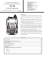
VX-7R
YAESU EUROPE B.V.
P.O. Box 75525, 1118 ZN Schiphol, The Netherlands
YAESU UK LTD.
Technical Supplement
Unit 12, Sun Valley Business Park, Winnall Close
Winchester, Hampshire, SO23 0LB, U.K.
VERTEX STANDARD HK LTD.
©2002 VERTEX STANDARD CO., LTD. Printed in Japan.
Unit 5, 20/F., Seaview Centre, 139-141 Hoi Bun Road,
Kwun Tong, Kowloon, Hong Kong
EH009M90A
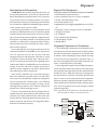
Introduction
DW
This manual provides the technical information necessary for servicing
the VX-7R 50/144/430 MHzTriple-Band Heavy Duty Submersible Transceiver.
Servicing this equipment requires expertise in handing surface-mount
chip components. Attempts by non-qualified persons to service this
equipment may result in permanent damage not covered by the warranty, and may be illegal in some countries.
Two PCB layout diagrams provided for each double-sided board in
this transceiver. Each side of the board is referred to by the type of the
majority of components installed on that side ("Side A" or "Side B"). In
most cases one side has only chip components, and the other has either
a mixture of both chip and leaded components (trimmers, coils, electrolytic capacitors, ICs, etc.), or leaded components only.
While we believe the information in this manual to be correct, VERTEX STANDARD assumes no liability for damage that may occur as a
result of typographical or other errors that may be present. Your cooperation in pointing out any inconsistencies in the technical information
would be appreciated.
Contents
Specification .................................................................................................................................... 2
Exploded View & Miscellaneous Parts ........................................................................................ 4
Block Diagram ................................................................................................................................. 5
Interconnection Diagram ............................................................................................................... 6
Circuit Description ........................................................................................................................ 7
Alignment ...................................................................................................................................... 11
Board Unit (Schematics, Layouts & Parts)
RF Unit .................................................................................................................................................................... 19
AF Unit .................................................................................................................................................................... 33
CNTL Unit .............................................................................................................................................................. 43
VCO Unit ................................................................................................................................................................ 53
1
Specifications
General
Frequency Ranges:
Channel Steps:
Frequency Stability:
Emission Type:
Antenna Impedance:
Supply Voltage:
Current Consumption:
Operating Temperature:
Case Size:
Weight:
2
Rx (MAIN):
0.5 - 1.8 MHz (BC Band)
1.8 - 30 MHz (SW Band)
30-59 MHz (50 MHz HAM: USA version)
30-76 MHz (50 MHz HAM: EXP version)
59-108 MHz (FM: USA version)
76-108 MHz (FM: EXP version)
108-137 MHz (Air Band)
137-174 MHz (144 MHz HAM)
174-222 MHz (VHF-TV)
222-225 MHz (220 MHz HAM: USA version)
225-420 MHz (ACT1: Action Band 1: USA version)
222-420 MHz (ACT1: Action Band 1: EXP version)
420-470 MHz (430 MHz HAM)
470-729 MHz (UHF-TV: USA version)
470-800 MHz (UHF-TV: EXP version)
800-999 MHz (ACT2: Action Band 2, cellular Blocked)
Rx (SUB):
50 - 54 MHz
137 - 174 MHz
420 - 470 MHz
Tx: 50 - 54 MHz (MAIN & SUB)
144 - 146 MHz or 144 - 148 MHz (MAIN & SUB)
222-225 MHz (MAIN, USA version)
430 - 440 MHz or 430 - 450 MHz (MAIN & SUB)
5/9/10/12.5/15/20/25/50/100 kHz
±5 ppm (+14°F to +122°F, –10°C to +50°C)
F2, F3, A3
50-ohm
Nominal: 7.4 V DC, Negative Ground
Operating: 10 - 16 V DC, Negative Ground (EXT DC jack)
150 mA (Mono Band Receive)
200 mA (Dual Band Receive)
55 mA (Mono Band Receive, Standby, Saver Off)
100 mA (Dual Band Receive, Standby, Saver Off)
25 mA (Mono Band Receive, Standby, Saver On "Save Ratio 1:5")
50 mA (Dual Band Receive, Standby, Saver On "Save Ratio 1:5")
400 µA (Auto Power Off)
1.6/1.3/1.0/0.7 A (50 MHz, Tx HI/L3/L2/L1)
1.71.4/1.1/0.8 A (144 MHz, Tx HI/L3/L2/L1)
0.6 A (220 MHz, Tx)
1.8/1.5/1.2/0.9/ A (430 MHz, Tx HI/L3/L2/L1)
–4°F to +140°F (–20°C to +60°C)
60 (W) x 90 (H) x 28 (D) mm (w/o knob & antenna)
250 g
Specifications
Transmitter
RF Power Output:
Modulation Type:
Maximum Deviation:
Spurious Emission:
Microphone Impedance:
5/2.5/1.0/0.5 W (50/144/430 MHz, FM)
0.3 W (220 MHz, FM)
1.0 W (50 MHz, FM)
FM: Variable Reactance
AM: Early Stage (Low Level)
±5/±2.5 kHz
At least 60 dB below (@ Tx 1W)
2 k-ohm
Receiver
Circuit Type:
Intermediate Frequencies:
Sensitivity:
Selectivity:
AF Output:
N-FM, AM: Double-Conversion Superheterodyne
W-FM: Triple-Conversion Superheterodyne
1st: 47.25 MHz (N-FM, AM)
45.8 MHz (W-FM)
2nd: 450 kHz (N-FM, AM)
10.7 MHz (W-FM)
3rd: 1 MHz (W-FM)
3.0 µV for 10 dB SINAD (0.5 - 30 MHz, AM)
0.5 µV for 12 dB SINAD (30 - 50 MHz, N-FM)
0.16 µV for 12 dB SINAD (50 - 54 MHz, N-FM)
15 kHz/35 kHz (-6 dB/-60 dB: N-FM, AM)
200 kHz/300 kHz (-6 dB/-20 dB: W-FM)
200 mW @ 8 ohm for 10 % THD (@ 7.4V DC)
400 mW @ 8 ohm for 10 % THD (@ 13.8V DC)
Specifications are subject to change without notice, and are guaranteed within amateur bands only.
3
Exploded View & Miscellaneous Parts
Â
Â
RA0417100
PANEL FRAME
Â
Â
RA03995000
WINDOW
RA03994000
DOUBLE FACE TAPE
RA0401600
O RING
No. VXSTD P/N
À U9900137
Á U9900138
 U07225120
à U9900136
Ä RA0304300
Å U00103002
Æ U00104002
Ç U9900140
È U44104002
É U9900141
U07125102
DISCRIPTION
BINDING HEAD SCREW M2X21.7 (W/ O RING)
BINDING HEAD SCREW M2X5 (W/ O RING)
PAN HEAD SCREW M2X2.5SUS#1
SPECIAL SCREW M2X2.35
WASHER
PAN HEAD SCREW M2X3NI
PAN HEAD SCREW M2X4NI
TAPTITE SCREW M2X6SUS#3
TAPTITE SCREW M2X4NI
TAPTITE SCREW M1.7X5NI#3
TAPTITE SCREW M1.7X2.5SUS#1
CP7346002 (USA)
CP7346003 (EXPORT)
CP7346004 (GERMANY)
PANEL ASS’Y
with RUBBER KNOB, MIC SHEET,
SP SHEET, SP, PROTECTOR L,
PROTECTOR R
RA0399800
LIGHT GUIDE (LED)
RA0400000
RUBBER PACKING
Q7000426
LCD MODULE
RA014250A
DOUBLE FACE TAPE (LCD)
RA0399100
LIGHT GUIDE (LED)
RA0399900
REFLECTOR SHEET
RA0405600
MIC HOLDER RUBBER
È
CNTL-Unit
È
È
Æ
É
È
É
Æ
AF-Unit
Æ
FR008330C
FPC CABLE
Æ
There is a direction in
WASHER.
RA0426800
O RING
RA0400200
STUD (X4 pcs)
RA0400900
O RING
SCREW
ÆÆ
WASHER
EXP CAP
RA0400500
EXT CAP
RA0292200
SPECIAL NUT
RA01403AA
LATCH NAIL
Å
Ã
Ä
Á
Ç Ç
CP7342003
REAR CASE ASS’Y
with SMA CONNECTOR ASS’Y,
TERMINAL BOARD ASS’Y,
RUBBER KNOB (PTT),
RUBBER KNOB (PTT)
Á
RA0426900
O RING
Á
RA0087900
SPECIAL NUT
RA0400600
CAP(SP/MIC)
RA0399700
HOLDER (PTT)
Á
RA0401200
ENCODER KNOB
RA0401900
VOLUME KNOB
À
À
RA0400100
RUBBER KNOB (PTT)
RA0140100
MASK SHEET
RA0141600
RUBBER PACKING
FNB-80LI
4
QTY.
2
4
4
1
1
1
6
2
4
2
2
Block Diagram
5
Interconnection Diagram
6
Circuit Description
The VX-7R consists of a RF-UNIT, a CNTL-UNIT and
an AF-UNIT. The RF-UNIT contains the receiver front
end, PLL IC, power and switching circuits, and the VCOUNIT for transmit and receive local signal oscillation.
The CNTL-UNIT contains the CPU, and audio ICs, and
the power circuitry for the LCD. The AF-UNIT contains
the IF, and audio ICs.
Receiver Signal Flow
The VX-7R includes five receiver front ends, each
optimized for a particular frequency range and mode
combination.
(1) Triplexer
Signals between 0.5 and 540 MHz received at the antenna terminal pass through a first low-pass filter composed of C1266, C1269, C1289, C1291, C1296, C1297,
L1059, L1060, L1067 and L1068.
Received 430-MHz signals, after passing through the
low-pass filter, are fed to the UHF T/R switch circuit composed of diode switch D1048 (RLS135), D1051 (1SV307).
Received 145-MHz signals, after passing through the
low-pass filter, are fed to the VHF T/R switch circuit composed of diode switch D1053 (RLS135), D1054 (1SV307).
Received 50-MHz signals, after passing through the
low-pass filter, are fed to the 50MHz T/R switch circuit
composed of diode switch D1058 (RLS135), D1059
(1SV307).
(2) 145-MHz Band and 76-300MHz Reception
Received signals between 76 and 300 MHz pass through
the Triplexer circuit, low-pass filter/high-pass filter circuit, VHF T/R switch circuit and protector diode D1002
(1SS362) before additional filtering by a band-pass filter prior to application to RF amplifier Q1004 (2SC5555).
The amplified RF signal is passed through a band-pass
filter to first mixer Q1012 (2SC5555). Meanwhile, VHF
output from the VCO-UNIT is amplified by Q1017
(2SC5374) and applied through diode T/R switch D1041
(DAN222) to mixer Q1012 as the first local signal.
The 47.25-MHz intermediate frequency product of the
mixer is delivered to the AF-UNIT.
The TUNE voltage from the CPU on the CNTL-UNIT
is amplified by DC amplifier Q3017 (NJU7007F2) and
applied to varactors D1020 and D1022 (HVC369B),
D1019, D1021, D1023, D1024, D1033 and D1036 (1SV325)
in the variable frequency band-pass filters. By changing
the electrostatic capacitance of the varactors, optimum
filter characteristics are provided for each specific operating frequency.
(3) 435-MHz Band and 222-540MHz Reception
Received signals between 222 and 540 MHz pass
through the Triplexer circuit, low-pass filter/high-pass
filter circuit, UHF T/R switch circuit and protector diode D1001 (1SS362) before additional filtering by a bandpass filter prior to application to RF amplifier Q1003
(2SC5555). The amplified RF signal is passed through a
band-pass filter, RF amplifier Q1006 (2SC5555) and
band-pass filter to first mixer Q1011 (2SC5555). Meanwhile, UHF output from the VCO-UNIT is amplified by
Q1016 (2SC5374) and applied through diode T/R switch
D1045 (HN2D01FU) to mixer Q1011 as the first local signal.
The 47.25-MHz intermediate frequency product of the
mixer is delivered to the AF-UNIT.
The TUNE voltage from the CPU on the CNTL-UNIT
is amplified by DC amplifier Q3017 and applied to varactors D1005, D1018, D1030 and D1031 (HVC358B) in
the variable frequency band-pass filters. By changing the
electrostatic capacitance of the varactors, optimum filter characteristics are provided for each specific operating frequency.
(4) 50-MHz-Band and 30-76 MHz Reception
Received signals between 30 and 76 MHz pass through
the Triplexer circuit, low-pass filter circuit, 50 MHz T/R
switch circuit and protector diode D1003 (1SS362) before additional filtering by a band-pass filter prior to
application to RF amplifier Q1005 (2SC5555). The amplified RF signal is passed through a band-pass filter to
first mixer Q1008 (2SC5555). Meanwhile, 50 MHz output from the VCO-UNIT is amplified by Q1018
(2SC5374) and applied through diode T/R switch D1046
(HN2D01FU) to mixer Q1008 as the first local signal.
The 47.25-MHz intermediate frequency product of the
mixer is delivered to the AF-UNIT.
The TUNE voltage from the CPU on the CNTL-UNIT
is amplified by DC amplifier Q3017 and applied to varactors D1025 and D1026 (1SV325) in the variable frequency band-pass filters. By changing the electrostatic capacitance of the varactors, optimum filter characteristics are
provided for each specific operating frequency.
7
Circuit Description
(5) 0.5 - 30 MHz Reception
Received signals between 0.5 and 30 MHz pass through
the Triplexer circuit, low-pass filter circuit, HF T/R switch
circuit and protector diode D1003 before additional filtering by a band-pass filter prior to application to RF
amplifier Q1009 (2SC4915-0). The amplified RF signal
is passed through a band-pass filter to first mixer Q1013
(2SC4915-0). Meanwhile, HF output from the VCOUNIT is amplified by Q1018 and applied through diode
T/R switch D1046 to mixer Q1013 as the first local signal.
The 47.25-MHz intermediate frequency product of the
mixer is delivered to the AF-UNIT.
The TUNE voltage from the CPU on the CNTL-UNIT
is amplified by DC amplifier Q3017 and applied to varactors D1013 (HVR100) in the variable frequency bandpass filters. By changing the electrostatic capacitance of
the varactors, optimum filter characteristics are provided for each specific operating frequency.
tal X1001 on the RF-UNIT is multiplied fourfold by Q2004
(2SC4915-0) and Q2012 (2SC4154E) to provide the 46.8MHz second local signal, applied to the Narrow IF IC.
Within the IC, this signal is mixed with the 47.25-MHz
first intermediate frequency signal to produce the 450
kHz second intermediate frequency.
This second IF is filtered by ceramic filter CF2002
(ALFYM450F=k) and amplified by the limiting amplifier within the Narrow IF IC before quadrature detection
by ceramic discriminator CD2001 (CDBM450C7).
Demodulated audio is passed from pin 9 of the Narrow IF IC through the "Mute" analog switch Q2029
(2SJ364) and squelch gate Q2036 (2SJ364) before de-emphasis at Q2028 (DTC144EE).
The resulting audio is amplified by AF amplifier Q2040
(TDA7233D) and fed through the MIC/EAR jack J2002
to internal speaker SP1001 or an external earphone.
(6) 540 - 999 MHz Reception
Received signals between 540 and 999 MHz pass
through the high-pass filter circuit, T/R switch D1004
(1SV271) prior to application to RF amplifier Q1002
(2SC5277). The amplified RF signal is passed through a
band-pass filter to first mixer Q1010 (2SC5277). Meanwhile, UHF output from the VCO-UNIT is amplified by
Q1016 and applied through diode T/R switch D1045 to
mixer Q1010 as the first local signal.
The 47.25-MHz intermediate frequency product of the
mixer is delivered to the AF-UNIT.
The TUNE voltage from the CPU on the CNTL-UNIT
(8) Squelch Control
Signal components in the neighborhood of 15 kHz contained in the discriminator output pass through an active band-pass filter composed of R2059, R2060, R2062,
C2076, C2078 and the operational amplifier between pins
7 and 8 within Narrow IF IC Q2016. They are then rectified by D2012 and D2013 (MC2850) to obtain a DC voltage corresponding to the level of noise. This voltage is
fed to pin 49 of CPU Q3035 (HD6472237TF10), which
compares the input voltage with a previously set threshold. When the input voltage drops below the threshold,
normally due to the presence of a carrier, the CPU turns
on squelch gate Q2036 and allows any demodulated au-
is amplified by DC amplifier Q3017 and applied to varactors D1015 and D1017 (HVC355B) in the variable fre-
dio to pass. At the same time, Q3001 and/or Q3003 and/
or Q3004 goes on, causing the BUSY/TX lamp D3033
quency band-pass filters. By changing the electrostatic
capacitance of the varactors, optimum filter characteris-
(FRGB1312CE-10-TF) to light.
tics are provided for each specific operating frequency.
(7) 47.25-MHz First Intermediate Frequency
The 47.25-MHz first intermediate frequency from the
first mixers is delivered from the RF-UNIT to the AFUNIT through jacks J1008 and J2001. On the AF-UNIT,
the IF for AM and FM-narrow signals is passed through
NAR/WIDE switch D2001 (DAP222) and the 47.25-MHz
monolithic crystal filter (MCF) XF2001 to narrow IF amplifier Q2002 (2SC4915-0) for input to pin 16 of the Narrow IF IC Q2016 (TA31136FN), after amplitude limiting
by D2003 (DA221).
Meanwhile, a portion of the output of 11.7-MHz crys-
8
Transmitter Signal Flow
(1) 145-MHz-Band Transmit/Receive Switching
Closing PTT switch S2002 on the AF-UNIT pulls the
base of Q3008 (DTA144EE) low, causing the collector to
go high. This signal is fed to pin 33 (PTT) of CPU Q3035,
allowing the CPU to recognize that the PTT switch has
been pushed. When the CPU detects closure of the PTT
switch, pin 10 (TX) goes high. This control signal is delivered to the RF-UNIT, where it switches Q1044 (UMW1)
and Q1043 (CPH6102) to produce the TX control signal
that activates Q1046 (2SA1774). At the same time, PLL
division data is fed to PLL IC Q1019 (MB15A01PFV1)
from the CPU, to disable the receiver power saver. Also,
Circuit Description
it switches Q1048 (KRC654U) to disable the receiver circuits. This causes the "red" mode of BUSY/TX lamp D3033
to light.
(2) Modulation
Voice signal input from either built-in microphone
MC3001 (EM-140) on the CNTL-UNIT or external jack
J2002 on the AF-UNIT is pre-emphasized by C3012 and
R3031, and processed by microphone amplifier Q3018
(NJM3403AV), IDC (instantaneous deviation control) circuit Q1014 to prevent overmodulation, and fed through
active low-pass filter Q1014.
During CTCSS operation, the voice signal is mixed with
the TONE ENC subaudible tone signal from pin 43 of
the CPU and delivered to the RF-UNIT through jacks
J3003 and J1008. During DTMF operation, the DTMF
tones from pin 44 of the CPU are fed to the IDC stage.
(3) 145-MHz-Band Transmission
Modulating audio from the CNTL-UNIT passes
through deviation setting D/A converter Q3012 to the
VHF modulator portion of the VCO-UNIT mounted on
the RF-UNIT. This signal is applied to varactor D4005
(HSC277) in the tank circuit of VHF VCO Q4004
(EC3H07B), which oscillates at the desired VHF transmitting frequency. The modulated VCO signal is buffered by amplifier Q4006 (EC3H07B) and Q1017 and delivered through VHF T/R diode switch D1041 to the RFUNIT. The modulated low-level VHF transmit signal
from the VCO is passed through diode switch D1043
(DAN222) to amplifier Q1014 (2SC5226-5). The modulated VHF transmit signal from the VCO is amplified by
Q1023 (2SK3475) and RF power amplifier Q1027
(2SK3476) up to 0.05, 1.0, 2.5 or 5 Watts (depending on
the power source). The RF output passes through TX
diode switch D1053. RF output is passed by the T/R
switch and low-pass filter to suppress harmonics and
spurious products before output gets to the antenna at
the antenna terminal.
ered by amplifier Q4006 and Q1016 and delivered
through UHF T/R diode switch D1045 to the RF-UNIT.
The modulated low-level UHF transmit signal from the
VCO is passed through diode switch D1045 (HN2D01FU)
to amplifier Q1014. The modulated UHF transmit signal
from the VCO is amplified by Q1023 and RF power amplifier Q1027 up to 0.05, 1.0, 2.5 or 5 Watts (depending
on the power source). The RF output passes through TX
diode switch D1048. RF output is passed through the T/
R switch and low-pass filter to suppress harmonics and
spurious products before output gets to the antenna at
the antenna terminal.
(5) 50-MHz-Band Transmission
Modulating audio from the CNTL-UNIT passes
through deviation setting D/A converter Q3012 to the 50
MHz modulator portion of the VCO-UNIT mounted on
the RF-UNIT. This signal is applied to varactor D4009
(HSC277) in the tank circuit of 50 MHz VCO Q4005
(EC3H07B), which oscillates at the desired 50 MHz transmitting frequency. The modulated VCO signal is buffered by amplifier Q4006 and Q1018 and delivered
through 50 MHz T/R diode switch D1046 to the RF-UNIT.
The modulated low-level 50 MHz transmit signal from
the VCO is passed through diode switch D1046
(HN2D01FU) to amplifier Q1014. The modulated 50 MHz
transmit signal from the VCO is amplified by Q1023 and
RF power amplifier Q1027 up to 0.05, 1.0, 2.5 or 5 Watts
(depending on the power source). The RF output passes
through TX diode switch D1058. RF output is passed
through the T/R switch and low-pass filter to suppress
harmonics and spurious products before output gets to
the antenna at the antenna terminal.
(4) 435-MHz-Band Transmission
Modulating audio from the CNTL-UNIT passes
through deviation setting D/A converter Q3012 to the
UHF modulator portion of the VCO-UNIT mounted on
the RF-UNIT. This signal is applied to varactor D4002
(HSC277) in the tank circuit of UHF VCO Q4002
(EC3H07B), which oscillates at the desired UHF transmitting frequency. The modulated VCO signal is buff-
9
Circuit Description
PLL Frequency Synthesizer
PLL IC Q1019 on the RF-UNIT consists of a data shift
register, reference frequency divider, phase comparator,
charge pump, "intermittent operation" circuit, and band
selector switch. Serial PLL data from the CPU is converted into parallel data by the shift register in the PLL
IC and is latched into the comparative frequency divider and reference frequency divider to set a frequency
dividing ratio for each. An 11.7-MHz reference signal
produced by X1001 is fed to "REF" pin 1 of the PLL IC.
The internal reference frequency divider divides the 11.7MHz reference by 2,050 (or 1,640) to obtain a reference
frequency of 5 kHz (or 6.25 kHz), which is applied to the
phase comparator. Meanwhile, a sample of the output
of VHF VCO Q4004 or UHF VCO Q4002 or 50 MHz VCO
Q4005 on the VCO-UNIT, buffered by Q4006, is fed to
the PLL IC, where it is divided by the internal comparative frequency divider to produce a comparative frequency which also is applied to the phase comparator. The
phase comparator compares the phase between the reference frequency and comparative frequency to output
10
a pulse corresponding to the phase difference between
them. This pulse is fed to the charge pump, and the output from the charge pump passes through a loop filter
composed of L1044, R1089, C1175, and either R1090,
C1192, R1103 and C1195 for VHF, or R1086, C1189, R1102
and C1194 for UHF, or R1091, C1193, R1104 and C1196
for 50 MHz, which convert the pulse into a corresponding smoothed varactor control voltage (VCV). The VCV
is applied to varactors D4004 and D4013 (1SV325) in the
VHF VCO tank circuit, or to varactor D4001 (HVC355B)
in the UHF VCO tank circuit, or to varactors D4007 and
D4008 (1SV325) in the 50 MHz VCO, to eliminate any
phase difference between the reference frequency and
comparative frequency, thus locking the VCO oscillation
frequency to the reference crystal. The VCO frequency
is determined by the frequency-dividing ratio sent from
the CPU to the PLL IC. During receiver power save operation, the PLL circuit operates intermittently to reduce
current consumption, for which the "intermittent operation" control circuit reduces the lock-up time.
Alignment
Introduction and Precautions
Required Test Equipment
The VX-7R has been carefully aligned at the factory for
the specified performance across the specified amateur
bands. Realignment should therefore not be necessary
except in the event of a component failure. All component replacement and service should be performed only
by an authorized VERTEX STANDARD representative,
or the warranty policy may be voided.
The following procedures cover the sometimes critical
and tedious adjustments that are not normally required
once the transceiver has left the factory. However, if damage occurs and some parts are replaced, realignment may
be required. If a sudden problem occurs during normal
operation, it is likely due to component failure; realignment should not be done until after the faulty component has been replaced.
We recommend that servicing be performed only by
authorized VERTEX STANDARD service technicians,
who are experienced with the circuitry and fully
equipped for repair and alignment. Therefore, if a fault
is suspected, contact the dealer from whom the transceiver was purchased for instructions regarding repair.
Authorized VERTEX STANDARD service technicians
realign all circuits and make complete performance
checks to ensure compliance with factory specifications
after replacing any faulty components.
Those who do undertake any of the following alignments are cautioned to proceed at their own risk. Problems caused by unauthorized attempts at realignment
are not covered by the warranty policy. Also, VERTEX
STANDARD must reserve the right to change circuits
and alignment procedures in the interest of improved
performance, without notifying owners.
Under no circumstances should any alignment be attempted unless the normal function and operation of the
transceiver are clearly understood, the cause of the malfunction has been clearly pinpointed and any faulty components replaced, and the need for realignment determined to be absolutely necessary.
m RF Signal Generator with calibrated output level at 500 MHz
m Deviation
Meter (linear detector)
In-line Wattmeter with 5% accuracy at 500 MHz
m 50-ohm, 10-W RF Dummy Load
m 8-ohm AF Dummy Load
m Regulated DC Power Supply adjustable from 3 to 15 V DC,
3A
m Frequency Counter: 0.2-ppm accuracy at 500 MHz
m AF Signal Generator
m AC Voltmeter
m DC Voltmeter: high impedance
m UHF Sampling Coupler
m SINAD Meter
m
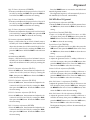
Alignment Preparation & Precautions
A 10-W RF dummy load and in-line wattmeter must
be connected to the main antenna jack in all procedures
that call for transmission, alignment is not possible with
an antenna. After completing one step, read the next step
to see if the same test equipment is required. If not, remove the test equipment (except dummy load and wattmeter, if connected) before proceeding.
Correct alignment requires that the ambient temperature be the same as that of the transceiver and test equipment, and that this temperature be held constant between
68~86°F (20~30°C). When the transceiver is brought into
the shop from hot or cold air, it should be allowed some
time to come to room temperature before alignment.
Whenever possible, alignments should be made with oscillator shields and circuit boards firmly affixed in place.
Also, the test equipment must be thoroughly warmed
up before beginning.
Note: Signal levels in dB referred to in the alignment procedure are based on 0 dBµ=0.5 µV (closed circuit).
RF Signal
Generator
50-ohm
RF Load
In-Line
Wattmeter
8-ohm
AF Load
Sampling
Coupler
SINAD
Meter
Deviation
Meter
Frequency
Counter
DW
Alignment Setup
11
Alignment
Test Setup
Set up the test equipment as shown below for transceiver alignment, and apply 8.7 V DC power to the transceiver. Refer to the drawings for Alignment Points.
Internal System Alignment Routine
This uses a programmed routine in the transceiver
which simplifies many previously complex discrete component settings and adjustments with digitally-controlled
settings via front panel buttons and LCD indications.
To begin, set the transceiver to the center of the 50 MHz,
144 MHz, 222 MHz and 430 MHz bands. Next, select the
430 MHz band, then turn the transceiver off.
Now, press and hold in the MON/F,
and 0 buttons
(at the same time) while powering the radio on again.
The display will show the first setting. Thereafter, the
frequencies used during alignment will automatically be
set without action by the technician.
In the alignment process, each adjustment is selected
by rotating the DIAL. Alignment is performed by:
m Pressing the V/M button;
m Injecting a signal of the required frequency and level; then
m Pressing the V/M button after a level setting or adjustment is made. This second pressing of the MON/
F button stores the entry.
To exit the alignment routine, press the HM/RV button. After performing the system alignment in its entirety, individual settings can be returned to and adjusted
should the need arise.
As each transceiver is individually optimized at the
factory, the precise settings for the transceiver on your
bench may be slightly different.
Main Band Alignment
PLL Reference Frequency (PLL REF)
Press the V/M button, then transmit and adjust the
counter frequency to 440.000 (±300 Hz) by rotating the
DIAL, then press the V/M button. Rotate the DIAL to select the next setting.
430 MHz band Alignment
Squelch Hysteresis Adjustment (HIS SQL)
m Rotate the DIAL for minimum squelch hysteresis. Press
the V/M button, then rotate the DIAL to select the next
setting.
12
Squelch Preset Threshold (THLD SQL) [86]
m Inject a –15.0 dBµ RF signal (1 kHz tone @ ±3.5 kHz
deviation), then press the V/M button, then press the
MON/F button twice. Press the V/M button, then rotate
the DIAL to select the next setting.
Squelch Preset Tight (TIGH SQL)
m Adjust the generator level to –4.0 dBµ, then press the
V/M button, then press the MON/F button twice. Press
the V/M button, then rotate the DIAL to select the next
setting.
S-Meter S-1 Adjustment (S1 LEVEL)
m Adjust the generator level to –7.0 dBµ (1 kHz tone @
±3.5 kHz deviation), then press the V/M button, then
press the MON/F button twice. Press the V/M button,
then rotate the DIAL to select the next setting.
S-Meter Full-Scale Adjustment (S9 LEVEL)
m Adjust the generator level to +20 dBµ (1 kHz tone @
±3.5 kHz deviation), then press the V/M button, then
press the MON/F button twice. Press the V/M button,
then rotate the DIAL to select the next setting.
Wide-FM S-Meter S-1 Adjustment (S1 LEVEL)
Adjust the generator level to 0 dBµ (1 kHz tone @ ±20
kHz deviation), then press the V/M button, then press
the MON/F button twice. Press the V/M button, then
rotate the DIAL to select the next setting.
m
Wide-FM S-Meter Full-Scale Adjustment (S9 LEVEL)
m Adjust the generator level to +20 dBµ (1 kHz tone @
±20 kHz deviation), then press the V/M button, then
press the MON/F button twice. Press the V/M button,
then rotate the DIAL to select the next setting.
The alignment frequency will now be automatically set
to 430.000 MHz.
High TX Power Adjustment (HI POWER)
m Transmit, and adjust the output power level for 5.0 W
(±0.3 W) by rotating the DIAL, then press the V/M button. Rotate the DIAL to select the next setting.
L3 Tx Power Adjustment (L3 POWER)
m Transmit, and adjust the output power level for 2.5 W
(±0.2 W) by rotating the DIAL, then press the V/M button. Rotate the DIAL to select the next setting.
L2 Tx Power Adjustment (L2 POWER)
m Transmit, and adjust the output power level for 1.0 W
(±0.1 W) by rotating the DIAL, then press the V/M button. Rotate the DIAL to select the next setting.
Alignment
L1 Tx Power Adjustment (L1 POWER)
m Transmit, and adjust the output power level for 50 mW
(+50/-30 mW) by rotating the DIAL, then press the V/M
button. Rotate the DIAL to select the next setting.
High TX Power Adjustment (L2 POWER)
m Transmit, and adjust the output power level for 1.0 W
(±0.1 W) by rotating the DIAL, then press the V/M button. Rotate the DIAL to select the next setting.
TX Deviation Adjustment (MAX DEV)
High TX Power Adjustment (L1 POWER)
m Transmit, and adjust the output power level for 50 mW
(+50/-30 mW) by rotating the DIAL, then press the V/M
button. Rotate the DIAL to select the next setting.
m
Inject a 1 kHz audio tone at a level of 50 mV (rms) to
the MIC jack. Press the V/M button, then transmit and
adjust the deviation for 4.5 kHz (±0.2 kHz) (USA Version: 4.2 kHz (±0.2 kHz)) by rotating the DIAL, then
press the V/M button. Rotate the DIAL to select the next
setting.
CTCSS Tx Deviation Adjustment (TN 67.0)
m Press the V/M button, then transmit and adjust the deviation for 0.5 kHz (+0.05/-0.1 kHz) by rotating the
DIAL, then press the V/M button. Rotate the DIAL to
select the next setting.
CTCSS Tx Deviation Adjustment (TN 183.5)
m Press the V/M button, then transmit and adjust the deviation for 0.5 kHz (±0.1 kHz) by rotating the DIAL,
then press the V/M button. Rotate the DIAL to select
the next setting.
CTCSS Tx Deviation Adjustment (TN 254.1)
m Press the V/M button, then transmit and adjust the deviation for 0.5 kHz (±0.1 kHz) by rotating the DIAL,
then press the V/M button. Rotate the DIAL to select
the next setting.
DCS Tx Deviation Adjustment (DCS DEV)
m Press the V/M button, then transmit and adjust the deviation for 0.6 kHz (±0.1 kHz) by rotating the DIAL,
then press the V/M button. Rotate the DIAL to select
the next setting.
Press the MON/F to activate the TX Power and Deviation alignment routine.
The alignment frequency will automatically be set to
440.000 MHz (USA Version: 450.000 MHz).
High TX Power Adjustment (HI POWER)
m Transmit, and adjust the output power level for 5.0 W
(±0.3 W) by rotating the DIAL, then press the V/M button. Rotate the DIAL to select the next setting.
High TX Power Adjustment (L3 POWER)
m Transmit, and adjust the output power level for 2.5 W
(±0.2 W) by rotating the DIAL, then press the V/M button. Rotate the DIAL to select the next setting.
TX Deviation Adjustment (MAX DEV)
m
Inject a 1 kHz audio tone at a level of 50mV (rms) to the
MIC jack. Press the V/M button, then transmit and adjust the deviation for 4.5 kHz (±0.2 kHz) (USA Version:
4.2 kHz (±0.2 kHz)) by rotating the DIAL, then press the
V/M button. Rotate the DIAL to select the next setting.
CTCSS Tx Deviation Adjustment (TN 67.0)
m Press the V/M button, then transmit and adjust the deviation for 0.5 kHz (+0.05/-0.1 kHz) by rotating the
DIAL, then press the V/M button. Rotate the DIAL to
select the next setting.
CTCSS Tx Deviation Adjustment (TN 183.5)
m Press the V/M button, then transmit and adjust the deviation for 0.5 kHz (±0.1 kHz) by rotating the DIAL,
then press the V/M button. Rotate the DIAL to select
the next setting.
CTCSS Tx Deviation Adjustment (TN 254.1)
m Press the V/M button, then transmit and adjust the deviation for 0.5 kHz (±0.1 kHz) by rotating the DIAL,
then press the V/M button. Rotate the DIAL to select
the next setting.
DCS Tx Deviation Adjustment (DCS DEV)
m Press the V/M button, then transmit and adjust the deviation for 0.6 kHz (±0.1 kHz) by rotating the DIAL,
then press the V/M button. Rotate the DIAL to select
the next setting.
Press the BAND button to activate the 50 MHz band
internal alignment routine.
The alignment frequency will automatically be set to
52.100 MHz.
50 MHz Band Alignment
Squelch Hysteresis Adjustment (HIS SQL)
m Rotate the DIAL for minimum squelch hysteresis. Press
the V/M button, then rotate the DIAL to select the next
setting.
13
Alignment
Squelch Preset Threshold (THLD SQL)
m Inject a –15.0 dBµ RF signal (1 kHz tone @ ±3.5 kHz
deviation), then press the V/M button, then press the
MON/F button twice. Press the V/M button, then rotate
the DIAL to select the next setting.
Squelch Preset Tight (TIGH SQL)
m Adjust the generator level to –4.0 dBµ, then press the V/M
button, then press the MON/F button twice. Press the V/
M button, then rotate the DIAL to select the next setting.
S-Meter S-1 Adjustment (S1 LEVEL)
m Adjust the generator level to –7.0 dBµ (1 kHz tone @
±3.5 kHz deviation), then press the V/M button, then
press the MON/F button twice. Press the V/M button,
then rotate the DIAL to select the next setting.
S-Meter Full-Scale Adjustment (S9 LEVEL)
m Adjust the generator level to +19 dBµ (1 kHz tone @
±3.5 kHz deviation), then press the V/M button, then
press the MON/F button twice. Press the V/M button,
then rotate the DIAL to select the next setting.
Wide-FM S-Meter S-1 Adjustment (S1 LEVEL)
m Adjust the generator level to 0 dBµ (1 kHz tone @ ±20
kHz deviation), then press the V/M button, then press
the MON/F button twice. Press the V/M button, then
rotate the DIAL to select the next setting.
Wide-FM S-Meter Full-Scale Adjustment (S9 LEVEL)
m Adjust the generator level to +20 dBµ (1 kHz tone @
±20 kHz deviation), then press the V/M button, then
press the MON/F button twice. Press the V/M button,
then rotate the DIAL to select the next setting.
The alignment frequency will now be automatically set
to 50.000 MHz.
High TX Power Adjustment (HI POWER)
m Transmit, and adjust the output power level for 5.0 W
(±0.3 W) by rotating the DIAL, then press the V/M button. Rotate the DIAL to select the next setting.
L3 Tx Power Adjustment (L3 POWER)
m Transmit, and adjust the output power level for 2.5 W
(±0.2 W) by rotating the DIAL, then press the V/M button. Rotate the DIAL to select the next setting.
L2 Tx Power Adjustment (L2 POWER)
m Transmit, and adjust the output power level for 1.0 W
(±0.1 W) by rotating the DIAL, then press the V/M button. Rotate the DIAL to select the next setting.
14
L1 Tx Power Adjustment (L1 POWER)
m Transmit, and adjust the output power level for 50 mW
(+50/-30 mW) by rotating the DIAL, then press the V/M
button. Rotate the DIAL to select the next setting.
TX Deviation Adjustment (MAX DEV)
m
Inject a 1 kHz audio tone at a level of 50mV (rms) to the
MIC jack. Press the V/M button, then transmit and adjust the deviation for4.5 kHz (±0.2 kHz) (USA Version:
(4.2 ±0.2 kHz)) by rotating the DIAL, then press the V/M
button. Rotate the DIAL to select the next setting.
AM Modulation (AM MOD)
m Inject a 1 kHz audio tone at a level of 100 mV (rms) to
the MIC jack. Press the V/M button, then transmit and
adjust the modulation for 60% (±10%) by rotating the
DIAL, then press and hold in the MON/F button for
one second.
CTCSS Tx Deviation Adjustment (TN 67.0)
m Press the V/M button, then transmit and adjust the deviation for 0.5 kHz (+0.05/-0.1 kHz) by rotating the
DIAL, then press the V/M button. Rotate the DIAL to
select the next setting.
CTCSS Tx Deviation Adjustment (TN 183.5)
m Press the V/M button, then transmit and adjust the deviation for 0.5 kHz (±0.1 kHz) by rotating the DIAL,
then press the V/M button. Rotate the DIAL to select
the next setting.
CTCSS Tx Deviation Adjustment (TN 254.1)
m Press the V/M button, then transmit and adjust the deviation for 0.5 kHz (±0.1 kHz) by rotating the DIAL,
then press the V/M button. Rotate the DIAL to select
the next setting.
DCS Tx Deviation Adjustment (DCS DEV)
m Press the V/M button, then transmit and adjust the deviation for 0.6 kHz (±0.1 kHz) by rotating the DIAL,
then press the V/M button. Rotate the DIAL to select
the next setting.
Press the MON/F button to activate the TX Power and
Deviation alignment routine.
The alignment frequency will automatically be set to
54.000 MHz.
High TX Power Adjustment (HI POWER)
m Transmit, and adjust the output power level for 5.0 W
(±0.3 W) by rotating the DIAL, then press the V/M button. Rotate the DIAL to select the next setting.
Alignment
High TX Power Adjustment (L3 POWER)
m Transmit, and adjust the output power level for 2.5 W
(±0.2 W) by rotating the DIAL, then press the V/M button. Rotate the DIAL to select the next setting.
Press the BAND button to activate the 145 MHz band
internal alignment routine.
The alignment frequency will automatically be set to
145.100 MHz (USA Version: 146.100 MHz).
High TX Power Adjustment (L2 POWER)
m Transmit, and adjust the output power level for 1.0 W
(±0.1 W) by rotating the DIAL, then press the V/M button. Rotate the DIAL to select the next setting.
144 MHz Band Alignment
High TX Power Adjustment (L1 POWER)
m Transmit, and adjust the output power level for 50 mW
(+50/-30 mW) by rotating the DIAL, then press the V/M
button. Rotate the DIAL to select the next setting.
TX Deviation Adjustment (MAX DEV)
Squelch Hysteresis Adjustment (HIS SQL)
m Rotate the DIAL for minimum squelch hysteresis. Press
the V/M button, then rotate the DIAL to select the next
setting.
Squelch Preset Threshold (THLD SQL)
m Inject a –15.0 dBµ RF signal (1 kHz tone @ ±3.5 kHz
deviation), then press the V/M button, then press the
MON/F button twice. Press the V/M button, then rotate
the DIAL to select the next setting.
Inject a 1 kHz audio tone at a level of 50mV (rms) to
the MIC jack. Press the V/M button, then transmit and
adjust the deviation for 4.5 kHz (±0.2 kHz) (USA Version: 4.2 kHz (±0.2 kHz)) by rotating the DIAL, then
press the V/M button. Rotate the DIAL to select the next
setting.
Squelch Preset Tight (TIGH SQL)
m Adjust the generator level to –4.0 dBµ, then press the
V/M button, then press the MON/F button twice. Press
the V/M button, then rotate the DIAL to select the next
setting.
AM Modulation (AM MOD)
m Inject a 1 kHz audio tone at a level of 100mV (rms) to
the MIC jack. Press the V/M button, then transmit and
adjust the modulation for 60% (±10%) by rotating the
DIAL.
S-Meter S-1 Adjustment (S1 LEVEL)
m Adjust the generator level to –7.0 dBµ (1 kHz tone @
±3.5 kHz deviation), then press the V/M button, then
press the MON/F button twice. Press the V/M button,
then rotate the DIAL to select the next setting.
CTCSS Tx Deviation Adjustment (TN 67.0)
m Press the V/M button, then transmit and adjust the deviation for 0.5 kHz (+0.05/-0.1 kHz) by rotating the
DIAL, then press the V/M button. Rotate the DIAL to
select the next setting.
S-Meter Full-Scale Adjustment (S9 LEVEL)
m Adjust the generator level to +19 dBµ (1 kHz tone @
±3.5 kHz deviation), then press the V/M button, then
press the MON/F button twice. Press the V/M button,
then rotate the DIAL to select the next setting.
CTCSS Tx Deviation Adjustment (TN 183.5)
m Press the V/M button, then transmit and adjust the de-
Wide-FM S-Meter S-1 Adjustment (S1 LEVEL)
m Adjust the generator level to 0 dBµ (1 kHz tone @ ±20
kHz deviation), then press the V/M button, then press
the MON/F button twice. Press the V/M button, then
rotate the DIAL to select the next setting.
m
viation for 0.5 kHz (±0.1 kHz) by rotating the DIAL,
then press the V/M button. Rotate the DIAL to select
the next setting.
CTCSS Tx Deviation Adjustment (TN 254.1)
m Press the V/M button, then transmit and adjust the deviation for 0.5 kHz (±0.1 kHz) by rotating the DIAL,
then press the V/M button. Rotate the DIAL to select
the next setting.
Wide-FM S-Meter Full-Scale Adjustment (S9 LEVEL)
m Adjust the generator level to +20 dBµ (1 kHz tone @
±20 kHz deviation), then press the V/M button, then
press the MON/F button twice. Press the V/M button,
then rotate the DIAL to select the next setting.
DCS Tx Deviation Adjustment (DCS DEV)
m Press the V/M button, then transmit and adjust the deviation for 0.6 kHz (±0.1 kHz) by rotating the DIAL,
then press the V/M button. Rotate the DIAL to select
the next setting.
The alignment frequency will now be automatically set
to 144.000 MHz.
15
Alignment
High TX Power Adjustment (HI POWER)
m Transmit, and adjust the output power level for 5.0 W
(±0.3 W) by rotating the DIAL, then press the V/M button. Rotate the DIAL to select the next setting.
Press the MON/F to activate the TX Power and Deviation alignment routine.
The alignment frequency will automatically be set to
146.000 MHz (USA Version: 148.000 MHz).
L3 Tx Power Adjustment (L3 POWER)
m Transmit, and adjust the output power level for 2.5 W
(±0.2 W) by rotating the DIAL, then press the V/M button. Rotate the DIAL to select the next setting.
High TX Power Adjustment (HI POWER)
m Transmit, and adjust the output power level for 5.0 W
(±0.3 W) by rotating the DIAL, then press the V/M button. Rotate the DIAL to select the next setting.
L2 Tx Power Adjustment (L2 POWER)
m Transmit, and adjust the output power level for 1.0 W
(±0.1 W) by rotating the DIAL, then press the V/M button. Rotate the DIAL to select the next setting.
High TX Power Adjustment (L3 POWER)
m Transmit, and adjust the output power level for 2.5 W
(±0.2 W) by rotating the DIAL, then press the V/M button. Rotate the DIAL to select the next setting.
L1 Tx Power Adjustment (L1 POWER)
m Transmit, and adjust the output power level for 50 mW
(+50/-30 mW) by rotating the DIAL, then press the V/M
button. Rotate the DIAL to select the next setting.
High TX Power Adjustment (L2 POWER)
m Transmit, and adjust the output power level for 1.0 W
(±0.1 W) by rotating the DIAL, then press the V/M button. Rotate the DIAL to select the next setting.
TX Deviation Adjustment (MAX DEV)
High TX Power Adjustment (L1 POWER)
m Transmit, and adjust the output power level for 50 mW
(+50/-30 mW) by rotating the DIAL, then press the V/M
button. Rotate the DIAL to select the next setting.
m
Inject a 1 kHz audio tone at a level of 50mV (rms) to
the MIC jack. Press the V/M button, then transmit and
adjust the deviation for 4.5 kHz (±0.2 kHz) (USA Version: 4.2 kHz (±0.2 kHz)) by rotating the DIAL, then
press the V/M button. Rotate the DIAL to select the next
setting.
CTCSS Tx Deviation Adjustment (TN 67.0)
m Press the V/M button, then transmit and adjust the deviation for 0.5 kHz (+0.05/-0.1 kHz) by rotating the
DIAL, then press the V/M button. Rotate the DIAL to
select the next setting.
CTCSS Tx Deviation Adjustment (TN 183.5)
m Press the V/M button, then transmit and adjust the deviation for 0.5 kHz (±0.1 kHz) by rotating the DIAL,
then press the V/M button. Rotate the DIAL to select
the next setting.
CTCSS Tx Deviation Adjustment (TN 254.1)
m Press the V/M button, then transmit and adjust the deviation for 0.5 kHz (±0.1 kHz) by rotating the DIAL,
then press the V/M button. Rotate the DIAL to select
the next setting.
DCS Tx Deviation Adjustment (DCS DEV)
m Press the V/M button, then transmit and adjust the deviation for 0.6 kHz (±0.1 kHz) by rotating the DIAL,
then press the V/M button. Rotate the DIAL to select
the next setting.
16
TX Deviation Adjustment (MAX DEV)
m
Inject a 1 kHz audio tone at a level of 50mV (rms) to
the MIC jack. Press the V/M button, then transmit and
adjust the deviation for 4.5 kHz (±0.2 kHz) (USA Version: 4.2 kHz (±0.2 kHz)) by rotating the DIAL, then
press the V/M button. Rotate the DIAL to select the next
setting.
CTCSS Tx Deviation Adjustment (TN 67.0)
m Press the V/M button, then transmit and adjust the deviation for 0.5 kHz (+0.05/-0.1 kHz) by rotating the
DIAL, then press the V/M button. Rotate the DIAL to
select the next setting.
CTCSS Tx Deviation Adjustment (TN 183.5)
m Press the V/M button, then transmit and adjust the deviation for for 0.5 kHz (±0.1 kHz) by rotating the DIAL,
then press the V/M button. Rotate the DIAL to select
the next setting.
CTCSS Tx Deviation Adjustment (TN 254.1)
m Press the V/M button, then transmit and adjust the deviation for 0.5 kHz (±0.1 kHz) by rotating the DIAL,
then press the V/M button. Rotate the DIAL to select
the next setting.
Alignment
DCS Tx Deviation Adjustment (DCS DEV)
m Press the V/M button, then transmit and adjust the deviation for 0.6 kHz (±0.1 kHz) by rotating the DIAL,
then press the V/M button. Rotate the DIAL to select
the next setting.
DCS Tx Deviation Adjustment (DCS DEV)
m Press the V/M button, then transmit and adjust the deviation for 0.6 kHz (±0.1 kHz) by rotating DIAL, then
press the V/M button. Rotate the DIAL to select the next
setting.
NOTE: The next step depends on the geographical "version"
of the transceiver being aligned:
Press the MON/F to activate the TX Power and Deviation alignment routine.
The alignment frequency will automatically be set to
224.995 MHz.
EXP Version: Alignment of the "SUB Band " follows
(see page 18.)
USA Version: Press the BAND button to activate the
222 MHz band internal alignment routine. In this case,
the alignment frequency will automatically be set to
222.000 MHz.
222 MHz Band Alignment
L2 Tx Power Adjustment (L2 POWER)
m Transmit, and adjust the output power level for 0.3 W
(±0.1 W) by rotating the DIAL, then press the V/M button. Rotate the DIAL to select the next setting.
L1 Tx Power Adjustment (L1 POWER)
m Transmit, and adjust the output power level for 50 mW
(+50/-30 mW) by rotating the DIAL, then press the V/M
button. Rotate the DIAL to select the next setting.
TX Deviation Adjustment (MAX DEV)
m
Inject a 1 kHz audio tone at a level of 50mV (rms) to
the MIC jack. Press the V/M button, then transmit and
adjust the deviation for 4.2 kHz (±0.2 kHz) by rotating
the DIAL, then press the V/M button. Rotate the DIAL
to select the next setting.
CTCSS Tx Deviation Adjustment (TN 67.0)
m Press the V/M button, then transmit and adjust the deviation for 0.5 kHz (+0.05/-0.1 kHz) by rotating the
DIAL, then press the V/M button. Rotate the DIAL to
select the next setting.
CTCSS Tx Deviation Adjustment (TN 183.5)
m Press the V/M button, then transmit and adjust the deviation for 0.5 kHz (±0.1 kHz) by rotating the DIAL,
then press the V/M button. Rotate the DIAL to select
the next setting.
CTCSS Tx Deviation Adjustment (TN 254.1)
m Press the V/M button, then transmit and adjust the deviation for 0.5 kHz (±0.1 kHz) by rotating the DIAL,
then press the V/M button. Rotate the DIAL to select
the next setting.
High Tx Power Adjustment (L2 POWER)
m Transmit, and adjust the output power level for 0.3 W
(±0.1 W) by rotating the DIAL, then press the V/M button. Rotate the DIAL to select the next setting.
High Tx Power Adjustment (L1 POWER)
m Transmit, and adjust the output power level for 50 mW
(+50/-30 mW) by rotating the DIAL, then press the V/M
button. Rotate the DIAL to select the next setting.
TX Deviation Adjustment (MAX DEV)
m
Inject a 1 kHz audio tone at a level of 50mV (rms) to
the MIC jack. Press the V/M button, then transmit and
adjust the deviation for 4.2 kHz ±0.2 kHz by rotating
DIAL, then press the V/M button. Rotate the DIAL to
select the next setting.
CTCSS Tx Deviation Adjustment (TN 67.0)
m Press the V/M button, then transmit and adjust the deviation for 0.5 kHz (+0.05/-0.1 kHz) by rotating the
DIAL, then press the V/M button. Rotate the DIAL to
select the next setting.
CTCSS Tx Deviation Adjustment (TN 183.5)
m Press the V/M button, then transmit and adjust the deviation for 0.5 kHz (±0.1 kHz) by rotating the DIAL,
then press the V/M button. Rotate the DIAL to select
the next setting.
CTCSS Tx Deviation Adjustment (TN 254.1)
m Press the V/M button, then transmit and adjust the deviation for 0.5 kHz (±0.1 kHz) by rotating the DIAL,
then press the V/M button. Rotate the DIAL to select
the next setting.
DCS Tx Deviation Adjustment (DCS DEV)
m Press the V/M button, then transmit and adjust the deviation for 0.6 kHz (±0.1 kHz) by rotating the DIAL,
then press the V/M button. Rotate the DIAL to select
the next setting.
17
Alignment
Press the SUB button to activate the SUB band internal alignment routine.
The alignment frequency will automatically be set to
435.100 MHz (USA Version: 440.100 MHz) on the SUB
band.
Squelch Preset Tight (TIGH SQL)
m Adjust the generator level to –4.0 dBµ, then press the
V/M button, then press the MON/F button twice. Press
the V/M button, then rotate the DIAL to select the next
setting.
SUB Band Alignment
430 MHz Band Alignment
S-Meter S-1 Adjustment (S1 LEVEL)
m Adjust the generator level to –7.0 dBµ (1 kHz tone @
±3.5 kHz deviation), then press the V/M button, then
press the MON/F button twice. Press the V/M button,
then rotate the DIAL to select the next setting.
Squelch Hysteresis Adjustment (HIS SQL)
m Rotate the DIAL for minimum squelch hysteresis. Press
the V/M button, then rotate the DIAL to select the next
setting.
Squelch Preset Threshold (THLD SQL)
m Inject a –13.0 dBµ RF signal (1 kHz tone @ ±3.5 kHz
deviation), then press the V/M button, then press the
MON/F button twice. Press the V/M button, then rotate
the DIAL to select the next setting.
Squelch Preset Tight (TIGH SQL)
m Adjust the generator level to –4.0 dBµ, then press the V/M
button, then press the MON/F button twice. Press the V/
M button, then rotate the DIAL to select the next setting.
S-Meter S-1 Adjustment (S1 LEVEL)
m Adjust the generator level to –7.0 dBµ (1 kHz tone @
±3.5 kHz deviation), then press the V/M button, then
press the MON/F button twice. Press the V/M button,
then rotate the DIAL to select the next setting.
S-Meter Full-Scale Adjustment (S9 LEVEL)
m Adjust the generator level to +20 dBµ (1 kHz tone @
±3.5 kHz deviation), then press the V/M button, then
press the MON/F button twice. Press the V/M button.
Press the BAND button to activate the 50 MHz SUB
band internal alignment routine.
The alignment frequency will automatically be set to
52.100 MHz.
50 MHz SUB Band Alignment
Squelch Hysteresis Adjustment (HIS SQL)
for minimum squelch hysteresis. Press
the V/M button, then rotate the DIAL to select the next
setting.
m Rotate the DIAL
Squelch Preset Threshold (THLD SQL)
m Inject a –13.0 dBµ RF signal (1 kHz tone @ ±3.5 kHz
deviation), then press the V/M button, then press the
MON/F button twice. Press the V/M button, then rotate
the DIAL to select the next setting.
18
S-Meter Full-Scale Adjustment (S9 LEVEL)
m Adjust the generator level to +19 dBµ (1 kHz tone @
±3.5 kHz deviation), then press the V/M button, then
press the MON/F button twice. Press the V/M button.
Press the BAND button to activate the 144 MHz SUB band
internal alignment routine.
The alignment frequency will automatically be set to
145.100 MHz (USA Version: 146.100 MHz).
144 MHz SUB Band Alignment
Squelch Hysteresis Adjustment (HIS SQL)
m Rotate the DIAL for minimum squelch hysteresis. Press the
V/M button, then rotate the DIAL to select the next setting.
Squelch Preset Threshold (THLD SQL)
m Inject a –15.0 dBµ RF signal (1 kHz tone @ ±3.5 kHz
deviation), then press the V/M button, then press the
MON/F button twice. Press the V/M button, then rotate
the DIAL to select the next setting.
Squelch Preset Tight (TIGH SQL)
m Adjust the generator level to –4.0 dBµ, then press the V/M
button, then press the MON/F button twice. Press the V/
M button, then rotate the DIAL to select the next setting.
S-Meter S-1 Adjustment (S1 LEVEL)
m Adjust the generator level to –7.0 dBµ (1 kHz tone @
±3.5 kHz deviation), then press the V/M button, then
press the MON/F button twice. Press the V/M button,
then rotate the DIAL to select the next setting.
S-Meter Full-Scale Adjustment (S9 LEVEL)
m Adjust the generator level to +19 dBµ (1 kHz tone @
±3.5 kHz deviation), then press the V/M button, then
presses the MON/F button twice. Press the V/M button.
This completes the internal alignment routine for all
bands. To save all settings and exit, press the HM/RV
button.
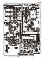
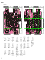
Circuit Diagram
MAIN NFM RX:+14.7dBµ
435.000MHz, @12dB SINAD
1000pF Coupling Capacitor.
800M RX:0.8V
800M RX:1.87V
145M TX:+5.1dBm
430M TX:+6.9dBm
1000pF Coupling Capacitor.
0V
(3.97V)
800M RX:0.73V
800M RX:1.61V
RF Unit
0V
(50M TX:1.84V)
(144M TX:1.85V)
(430M TX:2.85V)
0V
(1.98V)
0V
(1.86V)
13.5V
(13.3V)
MAIN NFM RX:+7.3dBµ
435.000MHz
1000pF Coupling Capacitor.
MAIN NFM RX:+2.0dBµ
435.000MHz
1000pF Coupling Capacitor.
430M RX:1.77V
(0V)
430M RX:1.89V
(0V)
0V
(1.24V)
0V
(50M:0.88V)
(144M:0.88V)
(430M:1.32V)
430M RX:1.05V (0V)
430M RX:0.66V
(0V)
430M RX:0.79V (0V)
0V
(5.22V)
430M RX:
0.81V
(0V)
0V
(2.27V)
0V
(50M:1.75V)
(144M:2.37V)
(430M:2.52V)
0V
(50M:0.8V)
(144M:0.82V)
(430M:1.29V)
0V
(1.42V)
0V
(50M:1.5V)
(144M:2.2V)
(430M:1.7V)
SUB NFM RX:+5.7dBµ
435.000MHz
1000pF Coupling Capacitor.
SUB430M RX:1.57V (0V)
0V (2.28V)
SUB430M RX:
2.14V (0V)
MAIN NFM RX:+11.5dBµ
SUB NFM RX:+7.1dBµ
145.000MHz
1000pF Coupling Capacitor.
0V
(50M:0.84V)
(144M:0.82V)
(430M:1.29V)
1.0V
(2.4V)
0.7V
(0.7V)
76~222M RX:1.81V (0V)
SUB430M RX:0.83V (0V)
76~222M RX:1.83V (0V)
76~222M RX:
0.73V (0V)
0.8V (0V)
0V
(50M:0.86V)
(144M:0.86V)
(430M:1.32V)
0V (50M TX:4.51V)
50M TX:+15.7dBm
1000pF Coupling Capacitor.
76~222M RX:1.37V
76~222M TX:1.08V
0V
(50M:2.44V)
76~222M RX:0.6V
76~222M TX:0.2V
0V
(50M:1.12V)
50M RX:0.35V
50M TX:0.45V
BC SW RX:0.79V
50M RX:1.31V
50M TX:3.9V
MAIN NFM RX:+4.3dBµ
SUB NFM RX:+3.5dBµ
52.000MHz
1000pF Coupling Capacitor.
SUB144M RX:2.4V (0V)
0V (0V)
50M RX:2.0V (0V)
50M RX:1.13V (0V)
1.88V
(1.92V)
0V (0V)
0.7V (0V)
50M RX:0.8V
50M RX:0.67V (0V)
6.4V
(6.4V)
0V (0V)
2.25V (2.3V)
1.3V
(1.3V)
13.4V
(13.3V)
0V (4.85V)
12.8V
(12.7V)
2.98V
(3.03V)
1.32V
(1.32V)
2.93V
(2.98V)
2.26V
(2.81V)
0V (0.48V)
2.9V
(2.9V)
0V (2.4V)
SUB50M RX:1.27V (0V)
BC SW RX:0.59V
BC SW RX:0.78V
BC SW RX:0.75V
0V (0V)
2.3V
(2.3V)
0V (2.95V)
2.12V
SAVE:0V
0V (0V)
76~222M RX:1.98V
76~222M TX:2.05V
430M: 1.99V
(2.01V)
50M: 1.99V
(2.07V)
0V (0V)
2.9V (2.9V)
UL:0V
BC SW RX:1.5V
2.78V (0V)
0V (0V)
0V (0V)
UL:2.9V
1.55V (1.6V)
SAVE:2.94V
0.66V
(0.66V)
0V (2.9V)
AM RX:+12dBµ
10dB SN
0.1µF Coupling Capacitor.
6.47V
(6.47V)
2.25V
(1.6V)
0V (5.5V)
50M RX:0V
0V (0V)
50M RX:0.45V
0V (2.9V)
(AMTX:2.38V)
0V (0V)
SW RX:2.95V
0.2V (0V)
430M RX:2.13V
0V~6.43V (0V)
0V (0V)
AM RX:2.61V
0V (2.5V)
(AMTX:0V)
0.66V (0V)
430M RX:2.7V
0V (0V)
AM:2.5V
(AM:2.5V)
50M: 2.77V
(0.48V)
0V (2.9V)
AMRX:1.84V
(AMTX:2.9V)
SHIFT ON:2.86V
SHIFT OFF:0V
0V (0V)
13.8V
(13.6V)
EXT DC IN 13.8V
:RX, ( ):TX
**
**
19
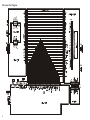
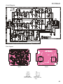
RF Unit
Parts Layout
A
B
C
D
a
b
CPH6102 (AB)
(Q1043)
DTA144EE (16)
(Q1021)
20
MB15A01PFV1
(Q1019)
KRX202U-RTK
(Q1015)
HN1J02FU (KS)
(Q1031)
UMW1 (W1)
(Q1044)
DTC143ZE (E23)
(Q1025)
DTC144EE (26)
(Q1001, 1026, 1029,
1030, 1034, 1035,
1042, 1051, 1053)
2SA1774 (FR)
(Q1033, 1036, 1038,
1046, 1052)
2SC4154E (LE)
(Q1032)
2SC5226 (LN)
(Q1014, 1024)
2SC5277 (D2)
(Q1002, 1010)
2SC5374 (NA)
(Q1016, 1017, 1018)
2SC4915 (QY)
(Q1008, 1009, 1013,
1020)
2SC5555ZD (ZD-)
(Q1003, 1004, 1005,
1006, 1007, 1011,
1012)
d
1
1
2
2
3
3
Side A
NJM12902V
(Q1022)
c
Side B
2SK3475
(Q1023)
KRC654U-RTK
(Q1040, 1048, 1049)
2SK3476
(Q1027)
KRA755U-RTK
(Q1047)
KRA760U-RTK
(Q1028, 1037, 1039,
1041, 1045, 1050)
DTC144TE-TL
(Q1054)
HN2D01FU (A1)
(D1045, 1046)
1SS362 (C3)
(D1001, 1002, 1003)
1SS321 (F9)
(D1047)
DAN222 (N)
(D1006, 1007, 1008,
1009, 1010, 1011,
1012, 1027, 1028,
1041, 1043, 1044,
1063)
1SS385 (09)
(D1050)
RF Unit
Parts List
REF.
C 1001
C 1002
C 1003
C 1004
C 1005
C 1006
C 1007
C 1008
C 1009
C 1010
C 1011
C 1013
C 1014
C 1015
C 1016
C 1017
C 1018
C 1019
C 1021
C 1023
C 1024
C 1025
C 1026
C 1027
C 1028
C 1029
C 1030
C 1031
C 1032
C 1033
C 1034
C 1035
C 1036
C 1037
C 1038
C 1040
C 1041
C 1042
C 1043
C 1044
C 1045
C 1046
C 1047
C 1048
C 1049
C 1051
C 1052
C 1053
C 1054
C 1055
C 1056
C 1057
C 1058
C 1059
C 1060
C 1061
DESCRIPTION
VALUE
V/W
PCB with Components (with VCO Unit)
PCB with Components (with VCO Unit)
PCB with Components (with VCO Unit)
Printed Circuit Board
CHIP CAP.
2pF
50V
CHIP CAP.
2pF
50V
CHIP CAP.
22pF
50V
CHIP CAP.
0.001uF
50V
CHIP CAP.
100pF
50V
CHIP CAP.
56pF
50V
CHIP CAP.
0.001uF
50V
CHIP CAP.
0.001uF
50V
CHIP CAP.
0.1uF
10V
CHIP CAP.
0.01uF
16V
CHIP CAP.
0.1uF
10V
CHIP CAP.
3pF
50V
CHIP CAP.
0.001uF
50V
CHIP CAP.
6pF
50V
CHIP CAP.
0.001uF
50V
CHIP CAP.
3pF
50V
CHIP CAP.
0.001uF
50V
CHIP CAP.
33pF
50V
CHIP CAP.
100pF
50V
CHIP CAP.
0.001uF
50V
CHIP CAP.
0.001uF
50V
CHIP CAP.
4pF
50V
CHIP CAP.
22pF
50V
CHIP CAP.
33pF
50V
CHIP CAP.
0.001uF
50V
CHIP CAP.
0.001uF
50V
CHIP CAP.
68pF
50V
CHIP CAP.
0.01uF
16V
CHIP CAP.
0.001uF
50V
CHIP CAP.
0.001uF
50V
CHIP CAP.
0.001uF
50V
CHIP CAP.
0.1uF
10V
CHIP CAP.
56pF
50V
CHIP CAP.
220pF
25V
CHIP CAP.
68pF
50V
CHIP CAP.
0.01uF
16V
CHIP CAP.
0.01uF
16V
CHIP CAP.
0.01uF
16V
CHIP CAP.
0.001uF
50V
CHIP CAP.
0.01uF
16V
CHIP CAP.
0.001uF
50V
CHIP CAP.
22pF
50V
CHIP CAP.
22pF
50V
CHIP CAP.
0.1uF
10V
CHIP CAP.
0.1uF
10V
CHIP CAP.
0.01uF
16V
CHIP CAP.
0.001uF
50V
CHIP CAP.
0.001uF
50V
CHIP CAP.
0.001uF
50V
CHIP CAP.
22pF
50V
CHIP CAP.
1pF
50V
CHIP CAP.
0.001uF
50V
CHIP CAP.
22pF
50V
CHIP CAP.
1pF
50V
CHIP CAP.
2pF
50V
CHIP CAP.
33pF
50V
TOL.
MFR’S DESIG
VXSTD P/N
VERS.
USA
EXPORT
GERMANY
CK
CK
CH
B
CH
CH
B
B
B
B
B
CJ
B
CH
B
CJ
B
CH
CH
B
B
CH
CH
CH
B
B
CH
B
B
B
B
B
CH
CH
CH
B
B
B
B
B
B
CH
CH
B
B
B
B
B
B
CH
CK
B
CH
CK
CK
CH
UMK105CK020CW-F
UMK105CK020CW-F
UMK105CH220JW-F
UMK105B102KW-F
UMK105CH101JW-F
UMK105CH560JW-F
UMK105B102KW-F
UMK105B102KW-F
GRM36B104K10PT
GRM36B103K16PT
GRM36B104K10PT
UMK105CJ030CW-F
UMK105B102KW-F
UMK105CH060DW-F
UMK105B102KW-F
UMK105CJ030CW-F
UMK105B102KW-F
UMK105CH330JW-F
UMK105CH101JW-F
UMK105B102KW-F
UMK105B102KW-F
UMK105CH040CW-F
UMK105CH220JW-F
UMK105CH330JW-F
UMK105B102KW-F
UMK105B102KW-F
UMK105CH680JW-F
GRM36B103K16PT
UMK105B102KW-F
UMK105B102KW-F
UMK105B102KW-F
GRM36B104K10PT
UMK105CH560JW-F
GRM36CH221J25PT
UMK105CH680JW-F
GRM36B103K16PT
GRM36B103K16PT
GRM36B103K16PT
UMK105B102KW-F
GRM36B103K16PT
UMK105B102KW-F
UMK105CH220JW-F
UMK105CH220JW-F
GRM36B104K10PT
GRM36B104K10PT
GRM36B103K16PT
UMK105B102KW-F
UMK105B102KW-F
UMK105B102KW-F
UMK105CH220JW-F
UMK105CK010CW-F
UMK105B102KW-F
UMK105CH220JW-F
UMK105CK010CW-F
UMK105CK020CW-F
UMK105CH330JW-F
FR008200C
K22178250
K22178250
K22178266
K22178829
K22178282
K22178276
K22178829
K22178829
K22108802
K22128804
K22108802
K22178251
K22178829
K22178254
K22178829
K22178251
K22178829
K22178270
K22178282
K22178829
K22178829
K22178252
K22178266
K22178270
K22178829
K22178829
K22178278
K22128804
K22178829
K22178829
K22178829
K22108802
K22178276
K22148203
K22178278
K22128804
K22128804
K22128804
K22178829
K22128804
K22178829
K22178266
K22178266
K22108802
K22108802
K22128804
K22178829
K22178829
K22178829
K22178266
K22178248
K22178829
K22178266
K22178248
K22178250
K22178270
LOT. SIDE LAY ADR.
CB7372002
CB7372003
CB7372004
11A
1A
1A
1A
1A
1B
1B
1B
1B
1B
1B
1A
1A
1A
1A
1A
1A
1A
1A
1A
1A
1A
1A
1B
1B
1A
1B
1B
1B
1B
1B
1B
1B
1B
1B
1B
1B
1B
1B
1B
1B
1B
1B
1B
1B
1B
1A
1A
1A
1A
1A
1A
1A
1A
1A
1A
A1
A1
B2
B2
B1
c2
c2
c1
c2
d2
d2
A1
A1
A2
A2
A2
A2
B1
B1
B1
B1
B1
B1
c2
c2
B2
c2
c2
b1
c2
c2
c2
c2
c2
c2
c2
d2
c2
d2
d3
d2
d2
d3
d2
d2
d3
C3
C3
C3
A2
B2
A2
A2
B2
B2
B2
21
RF Unit
REF.
C 1062
C 1063
C 1064
C 1065
C 1066
C 1067
C 1068
C 1069
C 1071
C 1072
C 1074
C 1075
C 1076
C 1077
C 1078
C 1079
C 1080
C 1081
C 1082
C 1083
C 1084
C 1085
C 1086
C 1087
C 1088
C 1089
C 1090
C 1091
C 1092
C 1093
C 1094
C 1095
C 1096
C 1097
C 1098
C 1099
C 1100
C 1101
C 1102
C 1103
C 1104
C 1105
C 1106
C 1107
C 1108
C 1109
C 1110
C 1111
C 1112
C 1113
C 1114
C 1115
C 1116
C 1117
C 1118
C 1119
C 1120
C 1121
C 1122
C 1123
22
DESCRIPTION
CHIP CAP.
CHIP CAP.
CHIP CAP.
CHIP CAP.
CHIP CAP.
CHIP CAP.
CHIP CAP.
CHIP CAP.
CHIP CAP.
CHIP CAP.
CHIP CAP.
CHIP CAP.
CHIP CAP.
CHIP CAP.
CHIP CAP.
CHIP CAP.
CHIP CAP.
CHIP CAP.
CHIP CAP.
CHIP CAP.
CHIP CAP.
CHIP CAP.
CHIP CAP.
CHIP CAP.
CHIP CAP.
CHIP CAP.
CHIP CAP.
CHIP CAP.
CHIP CAP.
CHIP CAP.
CHIP CAP.
CHIP CAP.
CHIP CAP.
CHIP CAP.
CHIP CAP.
CHIP CAP.
CHIP CAP.
CHIP CAP.
CHIP CAP.
CHIP CAP.
CHIP CAP.
CHIP CAP.
CHIP CAP.
CHIP CAP.
CHIP CAP.
CHIP CAP.
CHIP CAP.
CHIP CAP.
CHIP CAP.
CHIP CAP.
CHIP CAP.
CHIP CAP.
CHIP CAP.
CHIP CAP.
CHIP CAP.
CHIP CAP.
CHIP CAP.
CHIP CAP.
CHIP CAP.
CHIP CAP.
VALUE
4pF
4pF
0.001uF
0.001uF
22pF
8pF
6pF
10pF
8pF
22pF
8pF
8pF
0.001uF
0.001uF
22pF
68pF
22pF
0.001uF
82pF
120pF
12pF
3pF
22pF
0.001uF
8pF
0.01uF
0.001uF
100pF
0.001uF
68pF
3pF
0.001uF
100pF
5pF
0.001uF
5pF
22pF
0.001uF
1pF
0.1uF
27pF
82pF
0.1uF
27pF
0.01uF
0.01uF
12pF
0.5pF
7pF
0.001uF
33pF
1pF
2pF
33pF
2pF
0.001uF
0.1uF
8pF
9pF
6pF
V/W
50V
50V
50V
50V
50V
50V
50V
50V
50V
50V
50V
50V
50V
50V
50V
50V
50V
50V
50V
50V
50V
50V
50V
50V
50V
16V
50V
50V
50V
50V
50V
50V
50V
50V
50V
50V
50V
50V
50V
10V
50V
50V
10V
50V
16V
16V
50V
50V
50V
50V
50V
50V
50V
50V
50V
50V
10V
50V
50V
50V
TOL.
CH
CH
B
B
CH
CH
CH
CH
CH
CH
CH
CH
B
B
CH
CH
CH
B
CH
CH
CH
CJ
CH
B
CH
B
B
CH
B
CH
CJ
B
CH
CH
B
CH
CH
B
CK
B
CH
CH
B
CH
B
B
CH
CK
CH
B
CH
CK
CK
CH
CK
B
B
CH
CH
CH
MFR’S DESIG
UMK105CH040CW-F
UMK105CH040CW-F
UMK105B102KW-F
UMK105B102KW-F
UMK105CH220JW-F
UMK105CH080DW-F
UMK105CH060DW-F
UMK105CH100DW-F
UMK105CH080DW-F
UMK105CH220JW-F
UMK105CH080DW-F
UMK105CH080DW-F
UMK105B102KW-F
UMK105B102KW-F
UMK105CH220JW-F
UMK105CH680JW-F
UMK105CH220JW-F
UMK105B102KW-F
UMK105CH820JW-F
UMK105CH121JW-F
UMK105CH120JW-F
UMK105CJ030CW-F
UMK105CH220JW-F
UMK105B102KW-F
UMK105CH080DW-F
GRM36B103K16PT
UMK105B102KW-F
UMK105CH101JW-F
UMK105B102KW-F
UMK105CH680JW-F
UMK105CJ030CW-F
UMK105B102KW-F
UMK105CH101JW-F
UMK105CH050CW-F
UMK105B102KW-F
UMK105CH050CW-F
UMK105CH220JW-F
UMK105B102KW-F
UMK105CK010CW-F
GRM36B104K10PT
UMK105CH270JW-F
UMK105CH820JW-F
GRM36B104K10PT
UMK105CH270JW-F
GRM36B103K16PT
GRM36B103K16PT
UMK105CH120JW-F
UMK105CK0R5CW-F
UMK105CH070DW-F
UMK105B102KW-F
UMK105CH330JW-F
UMK105CK010CW-F
UMK105CK020CW-F
UMK105CH330JW-F
UMK105CK020CW-F
UMK105B102KW-F
GRM36B104K10PT
UMK105CH080DW-F
UMK105CH090DW-F
UMK105CH060DW-F
VXSTD P/N
K22178252
K22178252
K22178829
K22178829
K22178266
K22178256
K22178254
K22178258
K22178256
K22178266
K22178256
K22178256
K22178829
K22178829
K22178266
K22178278
K22178266
K22178829
K22178280
K22178284
K22178260
K22178251
K22178266
K22178829
K22178256
K22128804
K22178829
K22178282
K22178829
K22178278
K22178251
K22178829
K22178282
K22178253
K22178829
K22178253
K22178266
K22178829
K22178248
K22108802
K22178268
K22178280
K22108802
K22178268
K22128804
K22128804
K22178260
K22178247
K22178255
K22178829
K22178270
K22178248
K22178250
K22178270
K22178250
K22178829
K22108802
K22178256
K22178257
K22178254
VERS.
LOT. SIDE LAY ADR.
111111111111111111111111111111111111111111111111111111111111-
A
A
A
A
B
A
A
A
B
A
B
A
A
B
B
B
B
B
B
B
B
B
B
B
B
B
B
B
B
B
B
B
B
B
B
B
B
B
B
B
B
B
B
B
B
B
A
A
A
A
A
A
A
A
A
A
A
A
A
A
B2
B2
B2
B2
b2
B1
B2
B2
b2
B2
b2
B2
B2
b2
c2
c2
b2
b2
b2
b2
b2
b3
b3
b3
b3
c2
d2
c2
c3
c2
c2
c3
c2
c2
c3
c3
c3
c3
c3
d3
c2
c2
c3
c3
d3
d3
B2
B2
B2
A2
B2
B2
B2
B2
B2
C2
C2
B2
B2
B2
RF Unit
REF.
C 1124
C 1125
C 1126
C 1127
C 1128
C 1129
C 1130
C 1131
C 1132
C 1133
C 1134
C 1135
C 1136
C 1139
C 1142
C 1143
C 1145
C 1146
C 1147
C 1151
C 1152
C 1153
C 1154
C 1155
C 1156
C 1159
C 1160
C 1161
C 1162
C 1163
C 1164
C 1165
C 1166
C 1167
C 1170
C 1171
C 1172
C 1173
C 1174
C 1175
C 1178
C 1179
C 1180
C 1181
C 1182
C 1183
C 1184
C 1186
C 1187
C 1188
C 1189
C 1190
C 1190
C 1191
C 1192
C 1193
C 1194
C 1195
C 1196
C 1199
DESCRIPTION
CHIP CAP.
CHIP CAP.
CHIP CAP.
CHIP CAP.
CHIP CAP.
CHIP CAP.
CHIP CAP.
CHIP CAP.
CHIP CAP.
CHIP CAP.
CHIP CAP.
CHIP CAP.
CHIP CAP.
CHIP CAP.
CHIP CAP.
CHIP CAP.
CHIP CAP.
CHIP CAP.
CHIP CAP.
CHIP CAP.
CHIP CAP.
CHIP CAP.
CHIP CAP.
CHIP CAP.
CHIP CAP.
CHIP CAP.
CHIP CAP.
CHIP CAP.
CHIP CAP.
CHIP CAP.
CHIP CAP.
CHIP CAP.
CHIP CAP.
CHIP TA.CAP.
CHIP CAP.
CHIP CAP.
CHIP CAP.
CHIP CAP.
CHIP CAP.
CHIP TA.CAP.
CHIP CAP.
CHIP CAP.
CHIP CAP.
CHIP CAP.
CHIP CAP.
CHIP CAP.
CHIP CAP.
CHIP CAP.
CHIP CAP.
CHIP CAP.
CHIP TA.CAP.
CHIP CAP.
CHIP CAP.
CHIP CAP.
CHIP TA.CAP.
CHIP TA.CAP.
CHIP CAP.
CHIP CAP.
CHIP CAP.
CHIP CAP.
VALUE
56pF
0.001uF
6pF
2pF
0.001uF
0.001uF
0.1uF
0.01uF
0.1uF
0.01uF
10pF
0.01uF
0.01uF
0.001uF
0.001uF
0.001uF
22pF
0.001uF
0.001uF
0.001uF
1uF
0.01uF
220pF
0.01uF
22pF
0.001uF
47pF
0.001uF
0.001uF
0.1uF
0.01uF
47pF
0.001uF
22uF
0.1uF
0.01uF
47pF
10pF
0.001uF
1.5uF
33pF
15pF
0.001uF
0.01uF
47pF
0.001uF
0.001uF
0.001uF
0.01uF
0.01uF
0.1uF
12pF
12pF
1uF
0.1uF
0.1uF
0.001uF
0.01uF
0.033uF
0.001uF
V/W
50V
50V
50V
50V
50V
50V
10V
16V
10V
16V
50V
16V
16V
50V
50V
50V
50V
50V
50V
50V
10V
16V
50V
16V
50V
50V
50V
50V
50V
10V
16V
50V
50V
4V
10V
16V
50V
50V
50V
10V
50V
50V
50V
16V
50V
50V
50V
50V
16V
16V
20V
50V
50V
10V
20V
20V
50V
16V
10V
50V
TOL.
CH
B
CH
CK
B
B
B
B
B
B
CH
B
B
B
B
B
CH
B
B
B
F
B
B
B
CH
B
CH
B
B
B
B
CH
B
B
B
CH
CH
B
CH
CH
B
B
CH
B
B
B
B
B
CH
CH
F
B
B
B
B
MFR’S DESIG
UMK105CH560JW-F
UMK105B102KW-F
UMK105CH060DW-F
UMK105CK020CW-F
UMK105B102KW-F
UMK105B102KW-F
GRM36B104K10PT
GRM36B103K16PT
GRM36B104K10PT
GRM36B103K16PT
UMK105CH100DW-F
GRM36B103K16PT
GRM36B103K16PT
UMK105B102KW-F
UMK105B102KW-F
UMK105B102KW-F
UMK105CH220JW-F
UMK105B102KW-F
UMK105B102KW-F
UMK105B102KW-F
GRM39F105Z10PT
GRM36B103K16PT
UMK105B221KW-F
GRM36B103K16PT
UMK105CH220JW-F
UMK105B102KW-F
UMK105CH470JW-F
UMK105B102KW-F
UMK105B102KW-F
GRM36B104K10PT
GRM36B103K16PT
UMK105CH470JW-F
UMK105B102KW-F
TESVSP0G226M-8R
GRM36B104K10PT
GRM36B103K16PT
UMK105CH470JW-F
UMK105CH100DW-F
UMK105B102KW-F
TESVSP1A155M-8R
UMK105CH330JW-F
UMK105CH150JW-F
UMK105B102KW-F
GRM36B103K16PT
UMK105CH470JW-F
UMK105B102KW-F
UMK105B102KW-F
UMK105B102KW-F
GRM36B103K16PT
GRM36B103K16PT
SKF-1D104M-RP
UMK105CH120JW-F
UMK105CH120JW-F
GRM39F105Z10PT
SKF-1D104M-RP
SKF-1D104M-RP
UMK105B102KW-F
GRM36B103K16PT
GRM36B333K10PT
UMK105B102KW-F
VXSTD P/N
K22178276
K22178829
K22178254
K22178250
K22178829
K22178829
K22108802
K22128804
K22108802
K22128804
K22178258
K22128804
K22128804
K22178829
K22178829
K22178829
K22178266
K22178829
K22178829
K22178829
K22105001
K22128804
K22178821
K22128804
K22178266
K22178829
K22178274
K22178829
K22178829
K22108802
K22128804
K22178274
K22178829
K78060047
K22108802
K22128804
K22178274
K22178258
K22178829
K78100050
K22178270
K22178262
K22178829
K22128804
K22178274
K22178829
K22178829
K22178829
K22128804
K22128804
K78130049
K22178260
K22178260
K22105001
K78130049
K78130049
K22178829
K22128804
K22108803
K22178829
VERS.
USA
EXPORT
LOT. SIDE LAY ADR.
111111111111111111111111111111111111111111111111111121111111-
B
A
A
B
B
B
B
B
B
B
B
B
B
A
A
A
A
A
A
B
B
B
B
B
B
A
A
A
A
A
A
B
B
B
A
A
B
B
B
B
A
A
A
A
A
A
A
A
A
A
B
B
B
B
B
B
B
B
B
B
b2
B2
B2
a2
b3
b2
b2
c3
c3
c3
c3
c3
c3
B3
B3
A3
C2
C2
C2
a2
a2
a2
a2
a2
a2
A2
C2
C2
C2
D1
C2
a2
a2
a2
C3
C2
a2
a2
a2
a3
D2
D2
D1
C2
C2
D1
D1
C1
C2
C2
a3
a3
a3
b3
a3
b3
a3
b3
b3
a3
23
RF Unit
REF.
C 1200
C 1201
C 1202
C 1203
C 1205
C 1205
C 1205
C 1205
C 1206
C 1207
C 1207
C 1207
C 1207
C 1208
C 1208
C 1209
C 1210
C 1212
C 1213
C 1214
C 1215
C 1216
C 1218
C 1219
C 1220
C 1221
C 1222
C 1223
C 1224
C 1225
C 1226
C 1227
C 1228
C 1229
C 1230
C 1231
C 1232
C 1233
C 1234
C 1235
C 1236
C 1237
C 1238
C 1239
C 1240
C 1241
C 1242
C 1244
C 1245
C 1246
C 1247
C 1248
C 1249
C 1250
C 1251
C 1253
C 1254
C 1255
C 1256
C 1257
24
DESCRIPTION
CHIP CAP.
CHIP CAP.
CHIP CAP.
CHIP CAP.
CHIP CAP.
CHIP CAP.
CHIP CAP.
CHIP CAP.
CHIP CAP.
CHIP CAP.
CHIP CAP.
CHIP CAP.
CHIP CAP.
CHIP CAP.
CHIP CAP.
CHIP CAP.
CHIP CAP.
CHIP CAP.
CHIP TA.CAP.
CHIP CAP.
CHIP CAP.
CHIP CAP.
CHIP CAP.
CHIP CAP.
CHIP CAP.
CHIP CAP.
CHIP CAP.
CHIP CAP.
CHIP CAP.
CHIP CAP.
CHIP CAP.
CHIP CAP.
CHIP CAP.
CHIP CAP.
CHIP CAP.
CHIP CAP.
CHIP CAP.
CHIP CAP.
CHIP CAP.
CHIP CAP.
CHIP CAP.
CHIP CAP.
CHIP CAP.
CHIP CAP.
CHIP CAP.
CHIP CAP.
CHIP CAP.
CHIP CAP.
CHIP CAP.
CHIP CAP.
CHIP CAP.
CHIP CAP.
CHIP CAP.
CHIP CAP.
CHIP CAP.
CHIP CAP.
CHIP TA.CAP.
CHIP TA.CAP.
CHIP TA.CAP.
CHIP CAP.
VALUE
0.001uF
0.001uF
1uF
1uF
33pF
27pF
33pF
27pF
18pF
10pF
22pF
10pF
22pF
15pF
15pF
0.01uF
0.001uF
56pF
4.7uF
120pF
0.001uF
0.001uF
0.01uF
0.001uF
0.01uF
0.001uF
0.001uF
0.001uF
0.022uF
1uF
0.001uF
0.001uF
0.001uF
0.001uF
0.001uF
0.001uF
0.001uF
10pF
12pF
22pF
0.001uF
0.01uF
33pF
1pF
0.001uF
0.001uF
68pF
33pF
39pF
0.001uF
0.001uF
0.001uF
150pF
220pF
0.01uF
1uF
22uF
2.2uF
10uF
0.001uF
V/W
50V
50V
10V
10V
50V
50V
50V
50V
50V
50V
50V
50V
50V
50V
50V
16V
50V
50V
6.3V
50V
50V
50V
16V
50V
16V
50V
50V
50V
16V
10V
50V
50V
50V
50V
50V
50V
50V
50V
50V
50V
50V
16V
50V
50V
50V
50V
50V
50V
50V
50V
50V
50V
50V
25V
16V
10V
4V
4V
6.3V
50V
TOL.
B
B
F
F
CH
CH
CH
CH
CH
CH
CH
CH
CH
CH
CH
B
B
CH
CH
B
B
B
B
B
B
B
B
B
F
B
B
B
B
B
B
B
CH
CH
CH
B
B
CH
CK
B
B
CH
CH
CH
B
B
B
CH
CH
B
F
B
MFR’S DESIG
UMK105B102KW-F
UMK105B102KW-F
GRM39F105Z10PT
GRM39F105Z10PT
UMK105CH330JW-F
UMK105CH270JW-F
UMK105CH330JW-F
UMK105CH270JW-F
UMK105CH180JW-F
UMK105CH100DW-F
UMK105CH220JW-F
UMK105CH100DW-F
UMK105CH220JW-F
UMK105CH150JW-F
UMK105CH150JW-F
GRM36B103K16PT
UMK105B102KW-F
UMK105CH560JW-F
TESVSP0J475M-8R
UMK105CH121JW-F
UMK105B102KW-F
UMK105B102KW-F
GRM36B103K16PT
UMK105B102KW-F
GRM36B103K16PT
UMK105B102KW-F
UMK105B102KW-F
UMK105B102KW-F
GRM36B223K16PT
GRM39F105Z10PT
UMK105B102KW-F
UMK105B102KW-F
UMK105B102KW-F
UMK105B102KW-F
UMK105B102KW-F
UMK105B102KW-F
UMK105B102KW-F
UMK105CH100DW-F
UMK105CH120JW-F
UMK105CH220JW-F
UMK105B102KW-F
GRM36B103K16PT
UMK105CH330JW-F
UMK105CK010CW-F
UMK105B102KW-F
UMK105B102KW-F
GRM39CH680J50PT
UMK105CH330JW-F
UMK105CH390JW-F
UMK105B102KW-F
UMK105B102KW-F
UMK105B102KW-F
GRM39CH151J50PT
GRM36CH221J25PT
GRM36B103K16PT
GRM39F105Z10PT
TESVSP0G226M-8R
TESVSP0G225M-8R
TESVSP0J106M-8R
UMK105B102KW-F
VXSTD P/N
K22178829
K22178829
K22105001
K22105001
K22178270
K22178268
K22178270
K22178268
K22178264
K22178258
K22178266
K22178258
K22178266
K22178262
K22178262
K22128804
K22178829
K22178276
K78080053
K22178284
K22178829
K22178829
K22128804
K22178829
K22128804
K22178829
K22178829
K22178829
K22128806
K22105001
K22178829
K22178829
K22178829
K22178829
K22178829
K22178829
K22178829
K22178258
K22178260
K22178266
K22178829
K22128804
K22178270
K22178248
K22178829
K22178829
K22174231
K22178270
K22178272
K22178829
K22178829
K22178829
K22174239
K22148203
K22128804
K22105001
K78060047
K78060025
K78080055
K22178829
VERS.
GERMANY
USA
EXPORT
EXPORT
USA
EXPORT
EXPORT
GERMANY
EXPORT
GERMANY
LOT. SIDE LAY ADR.
111111121112111111111111111111111111111111111111111111111111-
B
B
B
B
A
A
A
A
A
A
A
A
A
A
A
B
A
A
A
A
A
A
A
A
A
B
A
A
B
B
B
A
A
A
A
B
A
A
A
A
A
A
A
A
A
A
B
B
B
A
B
B
B
B
B
A
A
B
A
A
b3
b3
b3
b3
C1
C1
C1
C1
C1
C1
C1
C1
C1
C1
C1
a1
C2
C1
C1
C1
C1
C1
B1
C2
B2
a1
D1
C3
a2
a2
a1
B3
A3
A2
B3
a1
C2
B1
B1
B1
A2
A2
B1
B1
B1
B1
b1
c1
c1
B1
c1
c2
b1
b1
c2
D2
A3
a1
A3
A3
RF Unit
REF.
C 1258
C 1259
C 1260
C 1262
C 1264
C 1266
C 1267
C 1269
C 1270
C 1271
C 1272
C 1273
C 1274
C 1275
C 1276
C 1277
C 1278
C 1279
C 1280
C 1281
C 1282
C 1283
C 1284
C 1285
C 1286
C 1287
C 1288
C 1289
C 1290
C 1291
C 1292
C 1293
C 1295
C 1296
C 1297
C 1298
C 1299
C 1301
C 1302
C 1303
C 1304
C 1305
C 1306
C 1307
C 1308
C 1309
C 1310
C 1310
C 1310
C 1310
C 1311
C 1312
C 1313
C 1314
C 1315
C 1316
C 1317
C 1319
C 1320
C 1322
DESCRIPTION
CHIP CAP.
CHIP CAP.
CHIP CAP.
CHIP CAP.
CHIP CAP.
CHIP CAP.
CHIP CAP.
CHIP CAP.
CHIP CAP.
CHIP CAP.
CHIP CAP.
CHIP CAP.
CHIP CAP.
CHIP CAP.
CHIP CAP.
CHIP CAP.
CHIP CAP.
CHIP CAP.
CHIP CAP.
CHIP CAP.
CHIP CAP.
CHIP CAP.
CHIP CAP.
CHIP CAP.
CHIP TA.CAP.
CHIP CAP.
CHIP CAP.
CHIP CAP.
CHIP CAP.
CHIP CAP.
CHIP CAP.
CHIP CAP.
CHIP CAP.
CHIP CAP.
CHIP CAP.
CHIP CAP.
CHIP CAP.
CHIP CAP.
CHIP CAP.
CHIP CAP.
CHIP CAP.
CHIP CAP.
CHIP CAP.
CHIP CAP.
CHIP CAP.
CHIP CAP.
CHIP CAP.
CHIP CAP.
CHIP CAP.
CHIP CAP.
AL.ELECTRO.CAP.
CHIP CAP.
CHIP CAP.
CHIP CAP.
CHIP CAP.
CHIP CAP.
CHIP CAP.
CHIP CAP.
CHIP CAP.
CHIP CAP.
VALUE
0.001uF
2pF
0.001uF
1pF
3pF
7pF
0.5pF
12pF
39pF
7pF
0.001uF
7pF
33pF
22pF
0.001uF
15pF
0.5pF
0.001uF
39pF
1pF
150pF
27pF
150pF
0.001uF
10uF
0.001uF
0.5pF
15pF
1pF
15pF
0.5pF
8pF
47pF
18pF
7pF
33pF
27pF
12pF
0.001uF
0.001uF
0.001uF
0.1uF
0.047uF
0.001uF
1uF
0.1uF
4pF
5pF
4pF
5pF
100uF
12pF
0.001uF
2pF
3pF
6pF
0.001uF
15pF
12pF
10pF
V/W
50V
50V
50V
50V
50V
50V
50V
50V
50V
50V
50V
50V
50V
50V
50V
50V
50V
50V
50V
50V
50V
50V
50V
50V
6.3V
50V
50V
50V
50V
50V
50V
50V
50V
50V
50V
50V
50V
50V
50V
50V
50V
10V
10V
50V
10V
10V
50V
50V
50V
50V
16V
50V
50V
50V
50V
50V
50V
50V
50V
50V
TOL.
B
CK
B
CK
CJ
CH
CK
CH
CH
CH
B
CH
CH
CH
B
CH
CK
B
CH
CK
CH
CH
CH
B
B
CK
CH
CK
CH
CK
CH
CH
CH
CH
CH
CH
CH
B
B
B
B
B
B
F
B
CH
CH
CH
CH
CH
B
CK
CJ
CH
B
CH
CH
CH
MFR’S DESIG
UMK105B102KW-F
UMK105CK020CW-F
UMK105B102KW-F
UMK105CK010CW-F
UMK105CJ030CW-F
UMK105CH070DW-F
GRM36CK0R5B50PT
UMK105CH120JW-F
UMK105CH390JW-F
UMK105CH070DW-F
UMK105B102KW-F
UMK105CH070DW-F
UMK105CH330JW-F
UMK105CH220JW-F
UMK105B102KW-F
UMK105CH150JW-F
GRM36CK0R5B50PT
UMK105B102KW-F
UMK105CH390JW-F
UMK105CK010CW-F
GRM36CH151J50PT
UMK105CH270JW-F
GRM36CH151J50PT
UMK105B102KW-F
TESVSP0J106M-8R
UMK105B102KW-F
GRM36CK0R5B50PT
UMK105CH150JW-F
UMK105CK010CW-F
UMK105CH150JW-F
GRM36CK0R5B50PT
UMK105CH080DW-F
UMK105CH470JW-F
UMK105CH180JW-F
UMK105CH070DW-F
UMK105CH330JW-F
UMK105CH270JW-F
UMK105CH120JW-F
UMK105B102KW-F
UMK105B102KW-F
UMK105B102KW-F
GRM36B104K10PT
GRM36B473K10PT
UMK105B102KW-F
GRM39F105Z10PT
GRM36B104K10PT
UMK105CH040CW-F
UMK105CH050CW-F
UMK105CH040CW-F
UMK105CH050CW-F
ECEV1CA101WP
UMK105CH120JW-F
UMK105B102KW-F
UMK105CK020CW-F
UMK105CJ030CW-F
UMK105CH060DW-F
UMK105B102KW-F
UMK105CH150JW-F
UMK105CH120JW-F
UMK105CH100DW-F
VXSTD P/N
K22178829
K22178250
K22178829
K22178248
K22178251
K22178255
K22178285
K22178260
K22178272
K22178255
K22178829
K22178255
K22178270
K22178266
K22178829
K22178262
K22178285
K22178829
K22178272
K22178248
K22178240
K22178268
K22178240
K22178829
K78080055
K22178829
K22178285
K22178262
K22178248
K22178262
K22178285
K22178256
K22178274
K22178264
K22178255
K22178270
K22178268
K22178260
K22178829
K22178829
K22178829
K22108802
K22108801
K22178829
K22105001
K22108802
K22178252
K22178253
K22178252
K22178253
K48120012
K22178260
K22178829
K22178250
K22178251
K22178254
K22178829
K22178262
K22178260
K22178258
VERS.
USA
EXPORT
EXPORT
GERMANY
LOT. SIDE LAY ADR.
111111111111111111111111111111111111111111111111211111111111-
A
A
A
A
B
A
B
A
A
B
B
B
B
B
B
B
B
B
B
B
B
B
B
B
B
B
A
A
B
A
B
A
A
A
A
B
B
B
B
B
B
B
B
A
A
A
A
A
A
A
A
A
A
A
A
A
B
B
B
A2
A1
A1
A1
c1
A1
c1
A1
A1
c1
c1
c1
c1
c1
c1
c1
c1
d1
d2
c1
d2
d1
d1
a2
a1
a1
A1
A1
d1
A1
d1
A1
A1
A1
A1
c1
c1
c1
a2
a2
a2
c1
c1
C1
C1
D1
C1
C1
C1
C1
B3
B2
B2
A2
B1
B2
b3
a3
d1
25
RF Unit
REF.
C 1323
D 1001
D 1002
D 1003
D 1004
D 1005
D 1006
D 1007
D 1008
D 1009
D 1010
D 1011
D 1012
D 1013
D 1014
D 1015
D 1017
D 1018
D 1019
D 1020
D 1021
D 1022
D 1023
D 1024
D 1025
D 1026
D 1027
D 1028
D 1029
D 1030
D 1031
D 1032
D 1033
D 1034
D 1035
D 1036
D 1037
D 1038
D 1039
D 1040
D 1041
D 1042
D 1043
D 1044
D 1045
D 1046
D 1047
D 1048
D 1049
D 1050
D 1051
D 1052
D 1053
D 1054
D 1055
D 1056
D 1057
D 1058
D 1059
D 1060
26
DESCRIPTION
CHIP CAP.
DIODE
DIODE
DIODE
DIODE
DIODE
DIODE
DIODE
DIODE
DIODE
DIODE
DIODE
DIODE
DIODE
DIODE
DIODE
DIODE
DIODE
DIODE
DIODE
DIODE
DIODE
DIODE
DIODE
DIODE
DIODE
DIODE
DIODE
DIODE
DIODE
DIODE
DIODE
DIODE
DIODE
DIODE
DIODE
DIODE
DIODE
DIODE
DIODE
DIODE
DIODE
DIODE
DIODE
DIODE
DIODE
DIODE
DIODE
DIODE
DIODE
DIODE
DIODE
DIODE
DIODE
DIODE
DIODE
DIODE
DIODE
DIODE
DIODE
VALUE
0.001uF
V/W
50V
TOL.
B
MFR’S DESIG
UMK105B102KW-F
1SS362 TE85R
1SS362 TE85R
1SS362 TE85R
1SV271 TPH3
HVC358B(TAPE)
DAN222 TL
DAN222 TL
DAN222 TL
DAN222 TL
DAN222 TL
DAN222 TL
DAN222 TL
HVR100-8TRU
M1FM3-4063
HVC355B(TAPE)
HVC355B(TAPE)
HVC358B(TAPE)
1SV325(TPH3)
HVC369B TRF
1SV325(TPH3)
HVC369B TRF
1SV325(TPH3)
1SV325(TPH3)
1SV325(TPH3)
1SV325(TPH3)
DAN222 TL
DAN222 TL
1SS400 TE61
HVC358B(TAPE)
HVC358B(TAPE)
1SS400 TE61
1SV325(TPH3)
1SS400 TE61
1SS400 TE61
1SV325(TPH3)
1SS400 TE61
1SS400 TE61
1SS400 TE61
1SS400 TE61
DAN222 TL
HVC359 TRF
DAN222 TL
DAN222 TL
HN2D01FUTE85R
HN2D01FUTE85R
1SS321 TE85R
RLS135 TE-11
RB751S-40TE61
1SS385(TE85L)
1SV307(TPH3)
1SV271 TPH3
RLS135 TE-11
1SV307(TPH3)
RB751S-40TE61
1SV271 TPH3
1SV271 TPH3
RLS135 TE-11
1SV307(TPH3)
1SS400 TE61
VXSTD P/N
K22178829
G2070268
G2070268
G2070268
G2070476
G2070590
G2070174
G2070174
G2070174
G2070174
G2070174
G2070174
G2070174
G2070540
G2070804
G2070588
G2070588
G2070590
G2070848
G2070872
G2070848
G2070872
G2070848
G2070848
G2070848
G2070848
G2070174
G2070174
G2070634
G2070590
G2070590
G2070634
G2070848
G2070634
G2070634
G2070848
G2070634
G2070634
G2070634
G2070634
G2070174
G2070708
G2070174
G2070174
G2070348
G2070348
G2070076
G2070128
G2070850
G2070880
G2070638
G2070476
G2070128
G2070638
G2070850
G2070476
G2070476
G2070128
G2070638
G2070634
VERS.
LOT. SIDE LAY ADR.
111111111111111111111111111111111111111111111111111111111111-
A
B
B
A
A
A
A
B
B
B
B
B
B
A
A
A
A
B
B
B
B
B
B
B
B
B
B
A
A
A
A
B
A
B
B
B
B
B
B
B
B
A
A
A
B
A
A
B
A
A
A
B
B
B
B
B
B
B
A
B1
c2
c2
A1
B1
B1
B1
c2
b2
c2
c2
d2
d2
C3
A2
A2
B2
b2
b2
b2
b2
b2
b2
c3
c3
d3
d3
A2
B2
B2
B2
b2
B2
b2
b2
c3
c3
c3
c3
b2
a2
C2
C2
C2
b2
A2
B1
c1
A3
B2
A1
c1
c1
c1
c1
c1
c1
c2
A3
RF Unit
REF.
D 1061
D 1062
D 1063
D 1064
FB1001
HS1001
J 1006
J 1007
J 1008
L 1001
L 1002
L 1003
L 1004
L 1005
L 1006
L 1007
L 1008
L 1009
L 1010
L 1011
L 1012
L 1013
L 1014
L 1015
L 1016
L 1017
L 1018
L 1019
L 1020
L 1021
L 1022
L 1023
L 1025
L 1026
L 1027
L 1028
L 1029
L 1030
L 1031
L 1032
L 1033
L 1034
L 1035
L 1036
L 1037
L 1038
L 1039
L 1040
L 1041
L 1042
L 1043
L 1044
L 1045
L 1046
L 1047
L 1048
L 1049
L 1049
L 1049
L 1049
DESCRIPTION
DIODE
DIODE
DIODE
DIODE
CHIP COIL
HEATSINK PLATE
CONNECTOR
CONNECTOR
CONNECTOR
M.RFC
M.RFC
M.RFC
M.RFC
M.RFC
M.RFC
M.RFC
M.RFC
M.RFC
M.RFC
M.RFC
M.RFC
M.RFC
M.RFC
M.RFC
M.RFC
M.RFC
M.RFC
M.RFC
M.RFC
M.RFC
M.RFC
M.RFC
M.RFC
M.RFC
M.RFC
M.RFC
M.RFC
M.RFC
M.RFC
M.RFC
M.RFC
M.RFC
M.RFC
M.RFC
M.RFC
M.RFC
M.RFC
M.RFC
M.RFC
M.RFC
M.RFC
M.RFC
M.RFC
M.RFC
CHIP COIL
M.RFC
M.RFC
M.RFC
M.RFC
M.RFC
VALUE
V/W
TOL.
MFR’S DESIG
RB751S-40TE61
1SV271 TPH3
DAN222 TL
1SS400 TE61
BLM21P300SPT
0.01uH
0.56uH
0.0082uH
0.01uH
0.033uH
0.0068uH
0.01uH
0.15uH
0.056uH
0.15uH
0.15uH
0.068uH
33uH
120uH
27uH
2.2uH
33uH
0.0056uH
0.0056uH
0.01uH
0.01uH
0.018uH
0.082uH
0.082uH
0.082uH
0.015uH
0.039uH
0.1uH
0.072uH
0.33uH
0.22uH
0.22uH
0.33uH
0.072uH
0.072uH
0.01uH
0.01uH
0.018uH
0.033uH
0.022uH
0.022uH
1uH
470uH
0.027uH
0.015uH
0.047uH
0.22uH
0.022uH
0.033uH
0.022uH
0.033uH
2%
5%
2%
2%
2%
2%
2%
2%
2%
2%
2%
2%
2%
2%
2%
5%
5%
2%
2%
2%
2%
2%
2%
AXK6F10335P
AXK6F10335P
IL-FPR-33S-VF-E1500
ELJ-RF10NJF2
LK1608 R56K-T
TFL0510-8N2
ELJ-RF10NJF2
C1608CA-33NG
C1608CA-6N8J
C1608CA-10NG
LK1608 R15K-T
HK1608 56NJ-T
LK1608 R15K-T
C1608CA-R15G
LK1608 68NM-T
LK1608 330M-T
FLC32T-121J
LK1608 270M-T
LK1608 2R2K-T
LK1608 330M-T
TFL0510-5N6
TFL0510-5N6
C1608CA-10NG
C1608CA-10NG
C1608CA-18NG
C1608CA-82NG
C1608CA-82NG
C1608CA-82NG
C1608CA-15NG
C1608CA-39NG
C1608CA-R10G
C1608CA-72NG
C1608CA-R33G
C1608CA-R22J
C1608CA-R22J
C1608CA-R33G
C1608CA-72NG
C1608CA-72NG
ELJ-RF10NJF2
C1608CA-10NG
C1608CA-18NG
C1608CA-33NG
TFL0510-22N
TFL0510-22N
LK1608 1R0K-T
FLC32T-471J
TFL0510-27N
TFL0510-15N
LQN21A47NJ04
LK1608 R22K-T
ELJ-RE22NJF2
ELJ-RE33NJF2
ELJ-RE22NJF2
ELJ-RE33NJF2
VXSTD P/N
G2070850
G2070476
G2070174
G2070634
L1690840
RA0395500
P0091225
P0091225
P1091138
L1690831
L1690415
L1690810
L1690831
L1691038
L1691093
L1691032
L1690409
L1690525
L1690409
L1691101
L1690406
L1690690
L1690228
L1691031
L1690634
L1690690
L1690808
L1690808
L1691032
L1691032
L1691035
L1691044
L1691044
L1691044
L1691034
L1691039
L1691045
L1691043
L1691106
L1691068
L1691068
L1691106
L1691043
L1691043
L1690831
L1691032
L1691035
L1691038
L1690815
L1690815
L1690687
L1690235
L1690816
L1690813
L1690617
L1690410
L1690718
L1690720
L1690718
L1690720
VERS.
USA
EXPORT
EXPORT
GERMANY
LOT. SIDE LAY ADR.
111111111111111111111111111111111111111111111111111111111121-
B
A
B
B
A
B
B
B
A
A
B
A
A
A
A
A
B
B
B
B
B
B
B
B
B
B
A
A
A
A
A
B
B
B
B
B
B
B
B
B
B
B
B
B
A
A
A
A
A
A
A
B
A
A
A
A
A
A
A
A
d1
A1
b2
a2
C3
b1
c2
b2
A2
A1
d2
A1
A1
B1
B1
B1
c2
c2
c2
c2
c2
c2
d2
d2
d2
d2
A2
A2
B2
B2
B2
b2
b2
b2
c2
b2
b2
b3
c3
c2
c3
c3
c2
c2
B2
B2
B2
B2
C2
C2
C2
a3
C2
D1
C1
C1
C1
C1
C1
C1
27
RF Unit
REF.
L 1050
L 1051
L 1052
L 1053
L 1054
L 1055
L 1056
L 1057
L 1058
L 1059
L 1060
L 1061
L 1062
L 1063
L 1064
L 1065
L 1066
L 1067
L 1068
L 1069
L 1070
L 1071
L 1072
L 1073
L 1074
L 1075
NF1001
Q 1001
Q 1002
Q 1003
Q 1004
Q 1005
Q 1006
Q 1007
Q 1008
Q 1009
Q 1010
Q 1011
Q 1012
Q 1013
Q 1014
Q 1015
Q 1016
Q 1017
Q 1018
Q 1019
Q 1020
Q 1021
Q 1022
Q 1023
Q 1024
Q 1025
Q 1026
Q 1027
Q 1028
Q 1029
Q 1030
Q 1031
Q 1032
Q 1033
28
DESCRIPTION
M.RFC
COIL
COIL
M.RFC
COIL
COIL
M.RFC
COIL
M.RFC
COIL
COIL
COIL
COIL
COIL
COIL
CHIP COIL
COIL
COIL
COIL
COIL
COIL
COIL
M.RFC
M.RFC
M.RFC
M.RFC
EMI FILTER
TRANSISTOR
TRANSISTOR
TRANSISTOR
TRANSISTOR
TRANSISTOR
TRANSISTOR
TRANSISTOR
TRANSISTOR
TRANSISTOR
TRANSISTOR
TRANSISTOR
TRANSISTOR
TRANSISTOR
TRANSISTOR
TRANSISTOR
TRANSISTOR
TRANSISTOR
TRANSISTOR
IC
TRANSISTOR
TRANSISTOR
IC
FET
TRANSISTOR
TRANSISTOR
TRANSISTOR
FET
TRANSISTOR
TRANSISTOR
TRANSISTOR
FET
TRANSISTOR
TRANSISTOR
VALUE
0.1uH
V/W
TOL.
2%
4.7uH
4.7uH
4.7uH
0.22uH
0.0068uH
0.0082uH
0.012uH
0.012uH
5%
MFR’S DESIG
C1608CA-R10G
E2 0.25-1.85-8.5T-L
E2 0.4-1.3-2T-L
LK1608 4R7K-T
E2 0.5-1.4-2.5T-L
E2 0.5-1.4-2.5T-L
LK1608 4R7K-T
E2 0.28-1.0-11TR
LK1608 4R7K-T
E2 0.35-1.4-3.5T-L-B
E2 0.35-1.4-3.5T-L-B
E2 0.35-1.6-4T-L
E2 0.35-1.6-7T-L
E2 0.35-1.6-7T-L
E2 0.35-1.6-7T-L
LQN21AR22J04
E2 0.25-1.85-8.5T-L
E2 0.35-1.6-4T-L
E2 0.35-1.6-4T-L
E2 0.3-1.7-7T-R
E2 0.35-1.6-7T-L
E2 0.25-1.9-10.5T-L
C1608CA-6N8J
HK1608 8N2J-T
TFL0510-12N
TFL0510-12N
NFM4516P13C204FT1
DTC144EE TL
2SC5277-D2-TL
2SC5555ZD-TR
2SC5555ZD-TR
2SC5555ZD-TR
2SC5555ZD-TR
2SC5555ZD-TR
2SC4915-O(TE85L)
2SC4915-O(TE85L)
2SC5277-D2-TL
2SC5555ZD-TR
2SC5555ZD-TR
2SC4915-O(TE85L)
2SC5226-5-TL
UMD6N TR
2SC5374-TL
2SC5374-TL
2SC5374-TL
MB15A01PFV1-G-BND-EF
2SC4915-O(TE85L)
DTA144EE TL
NJM12902V(TE1)
2SK3475(TE12L)
2SC5226-5-TL
DTC143ZE TL
DTC144EE TL
2SK3476(TE12L)
KRA760U-RTK
DTC144EE TL
DTC144EE TL
HN1J02FU(TE85L)
2SC4154-T11-1E
2SA1774 TL R
VXSTD P/N
L1691045
L0022576
L0022580
L1690688
L0022750
L0022750
L1690688
L0022426
L1690688
L0022729
L0022729
L0022456
L0022390
L0022390
L0022390
L1690600
L0022576
L0022456
L0022456
L0022372
L0022390
L0022749
L1691093
L1690515
L1690812
L1690812
Q9000759
G3070075
G3352778B
G3355557
G3355557
G3355557
G3355557
G3355557
G3349158O
G3349158O
G3352778B
G3355557
G3355557
G3349158O
G3352268E
G3070215
G3353748
G3353748
G3353748
G1092545
G3349158O
G3070074
G1093592
G3834758
G3352268E
G3070102
G3070075
G3834768
G3070278
G3070075
G3070075
G3070221
G3341548E
G3117748R
VERS.
LOT. SIDE LAY ADR.
111111111111111111111111111111111111111111111111111111111111-
A
A
A
A
B
B
B
B
B
A
A
A
B
B
B
B
B
A
A
B
B
B
A
A
A
A
A
A
A
A
B
B
A
A
B
B
A
A
B
B
A
A
A
B
B
B
B
B
A
A
A
A
B
A
A
A
A
B
A
A
C1
C1
B2
B1
b1
b1
c1
b1
c1
A1
A1
A1
c1
c1
c1
c2
d1
A1
A1
c1
d1
d1
C1
B2
B2
B2
C3
A2
A2
B1
c2
c2
B2
B2
c3
d3
A2
C2
b2
c3
C2
C2
C2
b2
b2
b2
a2
a2
D1
C1
C1
C2
a1
C1
C2
C2
C2
a1
A3
A3
RF Unit
REF.
Q 1034
Q 1035
Q 1036
Q 1037
Q 1038
Q 1039
Q 1040
Q 1041
Q 1042
Q 1043
Q 1044
Q 1045
Q 1046
Q 1047
Q 1048
Q 1049
Q 1050
Q 1051
Q 1052
Q 1053
Q 1054
R 1001
R 1002
R 1003
R 1005
R 1006
R 1007
R 1008
R 1009
R 1010
R 1011
R 1012
R 1013
R 1014
R 1015
R 1016
R 1017
R 1018
R 1019
R 1020
R 1021
R 1022
R 1023
R 1024
R 1025
R 1027
R 1028
R 1029
R 1030
R 1031
R 1032
R 1033
R 1034
R 1035
R 1036
R 1037
R 1038
R 1039
R 1040
R 1042
DESCRIPTION
TRANSISTOR
TRANSISTOR
TRANSISTOR
TRANSISTOR
TRANSISTOR
TRANSISTOR
TRANSISTOR
TRANSISTOR
TRANSISTOR
TRANSISTOR
TRANSISTOR
TRANSISTOR
TRANSISTOR
TRANSISTOR
TRANSISTOR
TRANSISTOR
TRANSISTOR
TRANSISTOR
TRANSISTOR
TRANSISTOR
TRANSISTOR
CHIP RES.
CHIP RES.
CHIP RES.
CHIP RES.
CHIP RES.
CHIP RES.
CHIP RES.
CHIP RES.
CHIP RES.
CHIP RES.
CHIP RES.
CHIP RES.
CHIP RES.
CHIP RES.
CHIP RES.
CHIP RES.
CHIP RES.
CHIP RES.
CHIP RES.
CHIP RES.
CHIP RES.
CHIP RES.
CHIP RES.
CHIP RES.
CHIP RES.
CHIP RES.
CHIP RES.
CHIP RES.
CHIP RES.
CHIP RES.
CHIP RES.
CHIP RES.
CHIP RES.
CHIP RES.
CHIP RES.
CHIP RES.
CHIP RES.
CHIP RES.
CHIP RES.
VALUE
1k
1k
1.5k
1k
3.3k
47k
220
47k
22
22
220
22k
22
22
4.7k
47
47k
220
1k
1k
2.2k
100k
1k
100k
100k
100k
100k
22k
100
100k
10k
100
100k
22
22
100k
100k
330k
100k
V/W
1/16W
1/16W
1/16W
1/16W
1/16W
1/16W
1/16W
1/16W
1/16W
1/16W
1/16W
1/16W
1/16W
1/16W
1/16W
1/16W
1/16W
1/16W
1/16W
1/16W
1/16W
1/16W
1/16W
1/16W
1/16W
1/16W
1/16W
1/16W
1/16W
1/16W
1/16W
1/16W
1/16W
1/16W
1/16W
1/16W
1/16W
1/16W
1/16W
TOL.
5%
5%
5%
5%
5%
5%
5%
5%
5%
5%
5%
5%
5%
5%
5%
5%
5%
5%
5%
5%
5%
5%
5%
5%
5%
5%
5%
5%
5%
5%
5%
5%
5%
5%
5%
5%
5%
5%
5%
MFR’S DESIG
DTC144EE TL
DTC144EE TL
2SA1774 TL R
KRA760U-RTK
2SA1774 TL R
KRA760U-RTK
KRC654U-RTK
KRA760U-RTK
DTC144EE TL
CPH6102-TL
UMW1 TR
KRA760U-RTK
2SA1774 TL R
KRA755U-RTK
KRC654U-RTK
KRC654U-RTK
KRA760U-RTK
DTC144EE TL
2SA1774 TL R
DTC144EE TL
DTC144TE-TL
RMC1/16S 102JTH
RMC1/16S 102JTH
RMC1/16S 152JTH
RMC1/16S 102JTH
RMC1/16S 332JTH
RMC1/16S 473JTH
RMC1/16S 221JTH
RMC1/16S 473JTH
RMC1/16S 220JTH
RMC1/16S 220JTH
RMC1/16S 221JTH
RMC1/16S 223JTH
RMC1/16S 220JTH
RMC1/16S 220JTH
RMC1/16S 472JTH
RMC1/16S 470JTH
RMC1/16S 473JTH
RMC1/16S 221JTH
RMC1/16S 102JTH
RMC1/16S 102JTH
RMC1/16S 222JTH
RMC1/16S 104JTH
RMC1/16S 102JTH
RMC1/16S 104JTH
RMC1/16S 104JTH
RMC1/16S 104JTH
RMC1/16S 104JTH
RMC1/16S 223JTH
RMC1/16S 101JTH
RMC1/16S 104JTH
RMC1/16S 103JTH
RMC1/16S 101JTH
RMC1/16S 104JTH
RMC1/16S 220JTH
RMC1/16S 220JTH
RMC1/16S 104JTH
RMC1/16S 104JTH
RMC1/16S 334JTH
RMC1/16S 104JTH
VXSTD P/N
G3070075
G3070075
G3117748R
G3070278
G3117748R
G3070278
G3070290
G3070278
G3070075
G3070223
G3070078
G3070278
G3117748R
G3070292
G3070290
G3070290
G3070278
G3070075
G3117748R
G3070075
G3070280
J24189025
J24189025
J24189027
J24189025
J24189031
J24189045
J24189017
J24189045
J24189005
J24189005
J24189017
J24189041
J24189005
J24189005
J24189033
J24189009
J24189045
J24189017
J24189025
J24189025
J24189029
J24189049
J24189025
J24189049
J24189049
J24189049
J24189049
J24189041
J24189013
J24189049
J24189037
J24189013
J24189049
J24189005
J24189005
J24189049
J24189049
J24189055
J24189049
VERS.
LOT. SIDE LAY ADR.
111111111111111111111111111111111111111111111111111111111111-
A
A
A
A
B
A
A
A
B
B
B
B
B
A
B
A
A
A
A
A
B
A
B
B
A
A
A
A
A
A
A
A
B
B
B
B
B
B
B
B
B
B
B
B
A
A
A
A
A
A
B
A
A
B
B
B
B
B
B
B
B2
A1
A3
B2
a1
B2
B3
B2
c1
a1
a1
a1
a1
C2
a1
D2
C2
C2
C2
C1
a1
B2
c2
c2
A1
A2
A2
A2
B1
B1
B1
B1
c2
c2
c2
c2
c2
c2
d2
d2
d2
d3
d2
d3
B2
B2
B2
B2
B2
B2
b2
B2
B2
c2
c2
c2
b2
b2
c3
c3
29
RF Unit
REF.
R 1043
R 1044
R 1045
R 1046
R 1049
R 1050
R 1051
R 1052
R 1052
R 1053
R 1054
R 1055
R 1056
R 1057
R 1058
R 1059
R 1060
R 1061
R 1062
R 1063
R 1064
R 1065
R 1066
R 1067
R 1068
R 1069
R 1069
R 1069
R 1069
R 1070
R 1071
R 1072
R 1073
R 1074
R 1075
R 1076
R 1077
R 1078
R 1079
R 1080
R 1081
R 1082
R 1083
R 1084
R 1085
R 1086
R 1087
R 1088
R 1089
R 1090
R 1090
R 1090
R 1090
R 1091
R 1092
R 1093
R 1094
R 1095
R 1096
R 1097
30
DESCRIPTION
CHIP RES.
CHIP RES.
CHIP RES.
CHIP RES.
CHIP RES.
CHIP RES.
CHIP RES.
CHIP RES.
CHIP RES.
CHIP RES.
CHIP RES.
CHIP RES.
CHIP RES.
CHIP RES.
CHIP RES.
CHIP RES.
CHIP RES.
CHIP RES.
CHIP RES.
CHIP RES.
CHIP RES.
CHIP RES.
CHIP RES.
CHIP RES.
CHIP RES.
CHIP RES.
CHIP RES.
CHIP RES.
CHIP RES.
CHIP RES.
CHIP RES.
CHIP RES.
CHIP RES.
CHIP RES.
CHIP RES.
CHIP RES.
CHIP RES.
CHIP RES.
CHIP RES.
CHIP RES.
CHIP RES.
CHIP RES.
CHIP RES.
CHIP RES.
CHIP RES.
CHIP RES.
CHIP RES.
CHIP RES.
CHIP RES.
CHIP RES.
CHIP RES.
CHIP RES.
CHIP RES.
CHIP RES.
CHIP RES.
CHIP RES.
CHIP RES.
CHIP RES.
CHIP RES.
CHIP RES.
VALUE
100k
1k
47k
330
330k
470
100k
1k
220
100k
330k
220
470
220
100k
220
330
220
100k
220
330
2.2k
330k
330
100
1k
680
680
1k
100
1k
1k
1k
330k
100k
100k
1M
10k
470
1k
47
10k
33k
33k
100
1.5k
1k
330k
1.8k
1.8k
1k
1.8k
1k
1k
47
27k
10k
470
10k
220k
V/W
1/16W
1/16W
1/16W
1/16W
1/16W
1/16W
1/16W
1/16W
1/16W
1/16W
1/16W
1/16W
1/16W
1/16W
1/16W
1/16W
1/16W
1/16W
1/16W
1/16W
1/16W
1/16W
1/16W
1/16W
1/16W
1/16W
1/16W
1/16W
1/16W
1/16W
1/16W
1/16W
1/16W
1/16W
1/16W
1/16W
1/16W
1/16W
1/16W
1/16W
1/16W
1/16W
1/16W
1/16W
1/16W
1/16W
1/16W
1/16W
1/16W
1/16W
1/16W
1/16W
1/16W
1/16W
1/16W
1/16W
1/16W
1/16W
1/16W
1/16W
TOL.
5%
5%
5%
5%
5%
5%
5%
5%
5%
5%
5%
5%
5%
5%
5%
5%
5%
5%
5%
5%
5%
5%
5%
5%
5%
5%
5%
5%
5%
5%
5%
5%
5%
5%
5%
5%
5%
5%
5%
5%
5%
5%
5%
5%
5%
5%
5%
5%
5%
5%
5%
5%
5%
5%
5%
5%
5%
5%
5%
5%
MFR’S DESIG
RMC1/16S 104JTH
RMC1/16S 102JTH
RMC1/16S 473JTH
RMC1/16S 331JTH
RMC1/16S 334JTH
RMC1/16S 471JTH
RMC1/16S 104JTH
RMC1/16S 102JTH
RMC1/16S 221JTH
RMC1/16S 104JTH
RMC1/16S 334JTH
RMC1/16S 221JTH
RMC1/16S 471JTH
RMC1/16S 221JTH
RMC1/16S 104JTH
RMC1/16S 221JTH
RMC1/16S 331JTH
RMC1/16S 221JTH
RMC1/16S 104JTH
RMC1/16S 221JTH
RMC1/16S 331JTH
RMC1/16S 222JTH
RMC1/16S 334JTH
RMC1/16S 331JTH
RMC1/16S 101JTH
RMC1/16S 102JTH
RMC1/16S 681JTH
RMC1/16S 681JTH
RMC1/16S 102JTH
RMC1/16S 101JTH
RMC1/16S 102JTH
RMC1/16S 102JTH
RMC1/16S 102JTH
RMC1/16S 334JTH
RMC1/16S 104JTH
RMC1/16S 104JTH
RMC1/16S 105JTH
RMC1/16S 103JTH
RMC1/16S 471JTH
RMC1/16S 102JTH
RMC1/16S 470JTH
RMC1/16S 103JTH
RMC1/16S 333JTH
RMC1/16S 333JTH
RMC1/16S 101JTH
RMC1/16S 152JTH
RMC1/16S 102JTH
RMC1/16S 334JTH
RMC1/16S 182JTH
RMC1/16S 182JTH
RMC1/16S 102JTH
RMC1/16S 182JTH
RMC1/16S 102JTH
RMC1/16S 102JTH
RMC1/16S 470JTH
RMC1/16S 273JTH
RMC1/16S 103JTH
RMC1/16S 471JTH
RMC1/16S 103JTH
RMC1/16S 224JTH
VXSTD P/N
J24189049
J24189025
J24189045
J24189019
J24189055
J24189021
J24189049
J24189025
J24189017
J24189049
J24189055
J24189017
J24189021
J24189017
J24189049
J24189017
J24189019
J24189017
J24189049
J24189017
J24189019
J24189029
J24189055
J24189019
J24189013
J24189025
J24189023
J24189023
J24189025
J24189013
J24189025
J24189025
J24189025
J24189055
J24189049
J24189049
J24189061
J24189037
J24189021
J24189025
J24189009
J24189037
J24189043
J24189043
J24189013
J24189027
J24189025
J24189055
J24189028
J24189028
J24189025
J24189028
J24189025
J24189025
J24189009
J24189042
J24189037
J24189021
J24189037
J24189053
VERS.
EXPORT
EXPORT
USA
GERMANY
GERMANY
USA
EXPORT
EXPORT
LOT. SIDE LAY ADR.
111111112111111111111111112111111111111111111111111121111111-
B
B
B
B
A
A
A
A
A
A
A
A
A
A
B
B
B
B
B
B
B
B
B
B
B
A
A
A
A
A
A
A
A
B
B
B
B
A
A
A
A
A
B
B
A
B
B
B
B
B
B
B
B
B
A
A
A
A
A
A
c3
d3
d3
d3
A2
A2
B2
A2
A2
B2
C2
C2
C2
B2
b2
b2
b2
b3
b2
c3
c3
c3
c3
c3
c3
C2
C2
C2
C2
C2
C3
C3
C3
a2
a2
a2
a2
C2
C2
C2
C2
C2
b2
b2
C2
a3
a2
a2
a3
a3
a3
a3
a3
b3
C2
D1
D1
D1
D2
D1
RF Unit
REF.
R 1098
R 1099
R 1100
R 1102
R 1103
R 1103
R 1103
R 1103
R 1104
R 1105
R 1106
R 1107
R 1108
R 1109
R 1110
R 1111
R 1112
R 1113
R 1114
R 1115
R 1116
R 1118
R 1119
R 1120
R 1121
R 1122
R 1123
R 1124
R 1125
R 1126
R 1127
R 1128
R 1129
R 1130
R 1131
R 1132
R 1133
R 1134
R 1135
R 1136
R 1137
R 1138
R 1139
R 1140
R 1141
R 1142
R 1143
R 1144
R 1145
R 1146
R 1147
R 1148
R 1149
R 1150
R 1151
TH1001
TH1002
X 1001
DESCRIPTION
CHIP RES.
CHIP RES.
CHIP RES.
CHIP RES.
CHIP RES.
CHIP RES.
CHIP RES.
CHIP RES.
CHIP RES.
CHIP RES.
CHIP RES.
CHIP RES.
CHIP RES.
CHIP RES.
CHIP RES.
CHIP RES.
CHIP RES.
CHIP RES.
CHIP RES.
CHIP RES.
CHIP RES.
CHIP RES.
CHIP RES.
CHIP RES.
CHIP RES.
CHIP RES.
CHIP RES.
CHIP RES.
CHIP RES.
CHIP RES.
CHIP RES.
CHIP RES.
CHIP RES.
CHIP RES.
CHIP RES.
CHIP RES.
CHIP RES.
CHIP RES.
CHIP RES.
CHIP RES.
CHIP RES.
CHIP RES.
CHIP RES.
CHIP RES.
CHIP RES.
CHIP RES.
CHIP RES.
CHIP RES.
CHIP RES.
CHIP RES.
CHIP RES.
CHIP RES.
CHIP RES.
CHIP RES.
CHIP RES.
THERMISTOR
THERMISTOR
XTAL TSS-6
TERMINAL PLATE
INSULATOR SHEET
VALUE
100
10k
330
3.3k
2.2k
1.5k
2.2k
1.5k
1k
12k
15k
100
4.7k
47
2.7k
100k
10k
47k
10k
47k
10k
330
3.3k
330
330
10k
4.7k
3.3k
1k
100k
4.7k
3.3k
3.3k
330
10k
4.7k
1k
4.7k
220
1k
10k
10k
1k
1k
10k
100
10k
22k
0
220
100k
100k
1k
10k
100
11.7MHz
V/W
1/16W
1/16W
1/16W
1/16W
1/16W
1/16W
1/16W
1/16W
1/16W
1/16W
1/16W
1/16W
1/16W
1/16W
1/16W
1/16W
1/16W
1/16W
1/16W
1/16W
1/16W
1/16W
1/16W
1/16W
1/16W
1/16W
1/16W
1/16W
1/16W
1/16W
1/16W
1/16W
1/16W
1/16W
1/16W
1/16W
1/16W
1/16W
1/16W
1/16W
1/16W
1/16W
1/16W
1/16W
1/16W
1/16W
1/16W
1/16W
1/16W
1/16W
1/16W
1/16W
1/16W
1/16W
1/16W
TOL.
5%
5%
5%
5%
5%
5%
5%
5%
5%
5%
5%
5%
5%
5%
5%
5%
5%
5%
5%
5%
5%
5%
5%
5%
5%
5%
5%
5%
5%
5%
5%
5%
5%
5%
5%
5%
5%
5%
5%
5%
5%
5%
5%
5%
5%
5%
5%
5%
5%
5%
5%
5%
5%
5%
5%
MFR’S DESIG
VXSTD P/N
RMC1/16S 101JTH
RMC1/16S 103JTH
RMC1/16S 331JTH
RMC1/16S 332JTH
RMC1/16S 222JTH
RMC1/16S 152JTH
RMC1/16S 222JTH
RMC1/16S 152JTH
RMC1/16S 102JTH
RMC1/16S 123JTH
RMC1/16S 153JTH
RMC1/16S 101JTH
RMC1/16S 472JTH
RMC1/16S 470JTH
RMC1/16S 272JTH
RMC1/16S 104JTH
RMC1/16S 103JTH
RMC1/16S 473JTH
RMC1/16S 103JTH
RMC1/16S 473JTH
RMC1/16S 103JTH
RMC1/16S 331JTH
RMC1/16S 332JTH
RMC1/16S 331JTH
RMC1/16S 331JTH
RMC1/16S 103JTH
RMC1/16S 472JTH
RMC1/16S 332JTH
RMC1/16S 102JTH
RMC1/16S 104JTH
RMC1/16S 472JTH
RMC1/16S 332JTH
RMC1/16S 332JTH
RMC1/16S 331JTH
RMC1/16S 103JTH
RMC1/16S 472JTH
RMC1/16S 102JTH
RMC1/16S 472JTH
RMC1/16S 221JTH
RMC1/16S 102JTH
RMC1/16S 103JTH
RMC1/16S 103JTH
RMC1/16S 102JTH
RMC1/16S 102JTH
RMC1/16S 103JTH
RMC1/16S 101JTH
RMC1/16S 103JTH
RMC1/16S 223JTH
RMC1/16 000JATP
RMC1/16S 221JTH
RMC1/16S 104JTH
RMC1/16S 104JTH
RMC1/16S 102JTH
RMC1/16S 103JTH
RMC1/16S 101JTH
ERTJ1VV473J
ERTJ1VV473J
TSS-5032A 11.7MHZ
J24189013
J24189037
J24189019
J24189031
J24189029
J24189027
J24189029
J24189027
J24189025
J24189038
J24189039
J24189013
J24189033
J24189009
J24189030
J24189049
J24189037
J24189045
J24189037
J24189045
J24189037
J24189019
J24189031
J24189019
J24189019
J24189037
J24189033
J24189031
J24189025
J24189049
J24189033
J24189031
J24189031
J24189019
J24189037
J24189033
J24189025
J24189033
J24189017
J24189025
J24189037
J24189037
J24189025
J24189025
J24189037
J24189013
J24189037
J24189041
J24185000
J24189017
J24189049
J24189049
J24189025
J24189037
J24189013
G9090122
G9090122
H0103264
RA0287100
RA0408300
VERS.
GERMANY
USA
EXPORT
EXPORT
LOT. SIDE LAY ADR.
111111121111111111111111111111111111111111111111111111111111-
A
A
A
B
B
B
B
B
B
B
B
A
A
A
A
B
B
B
B
B
B
A
B
B
B
B
B
B
A
B
A
A
A
B
B
A
B
B
A
B
B
B
B
A
B
A
A
A
A
B
B
B
B
A
A
B
A
B
C1
C1
C1
a3
a3
a3
a3
a3
b3
a1
a1
C1
C1
C2
D2
a2
a2
a2
a2
a2
a1
B1
c1
c1
c2
a2
a1
a1
A3
a1
A3
A1
A1
c1
c1
A3
a1
d1
A1
a2
a2
a2
a1
D2
c1
C1
C1
C1
B1
c3
a1
a1
d2
C3
C2
a2
C1
a2
31
RF Unit
Note:
32
AF Unit
Circuit Diagram
2.3V (0V)
2.2V (0V)
WFM RX:2.94V
BUSY:3.0V
0V (0V)
NFM:2.55V
(0V)
NFM:0.65V
(0V)
2.4V (0V)
WFM RX:2.2V
NFM:0.73V
(0V)
12.8V (12.5V)
BUSY:2.48V
0V (0V)
WFM RX:2.95V
(0V)
WFM RX:2.75V
(0V)
MAIN WFM RX:+7.4dBµ
@45.8MHz
1000pF Coupling Capacitor.
BUSY:3.0V
0V (0V)
2.8V (0V)
1.6V (1.6V)
BUSY:0V
2.73V (2.76V)
0.94V
(0V)
2.02V (0V)
AM:0.42V
(AM:0.42V)
0.63V
(0.63V)
0V (0V)
0.77V (0.45V)
WFM RX:0.73V
(0V)
1.6V
(0V)
MAIN RX:+10.5dBµ
@47.25MHz
0.01µF Coupling Capacitor.
WFM RX:2.68V
(0V)
WFM RX:0.68V
(0V)
0V (0V)
0V (0V)
1.17V (1.17V)
BUSY:0V
3.0V (3.0v)
2.5V (0V)
2.8V
(0V)
SUB 50M:0.82V
SUB 144M:0.67V
SUB 430M:0.83V
(0V)
BUSY:0V
3.0V (3.0V)
2.94V
(2.94V)
DUAL:2.84V
(0V)
0V (0V)
2.8V
(2.8V)
AM RX:1.29V
(0V)
DUAL:1.0V
(0V)
DUAL:0.97V
(0V)
1.39V
(0V)
0.604V
(0V)
0.5V
(0.5V)
SUB RX:+6.3dBµ
@46.35MHz
0.01µF Coupling Capacitor.
DUAL:0.94V
(0V)
DUAL:2.0V
(0V)
DUAL RX:2.8V (0V) DUAL:2.48V (0V)
AM RX:0.72V
(0V)
AM RX:0.635V
(0V)
DUAL RX:0.65V
SUB BUSY:0V
(0V)
3.0V (3.0V)
DUAL:1.25V
(0V)
0V (0V)
DUAL RX:1.63V
(0V)
AM RX:0.124V
(0V)
WFM RX:2.58V
(0V)
SUB BUSY:0V
3.0V (3.0V)
0V
(0V)
AM RX:0.927V
(0V)
0V (0V)
NFM AM RX:2.8V
WFM RX:0V
(0V)
WFM RX:0.47V
(0V)
0V (0V)
1.12V
(0V)
2.5V
(0V)
WFM RX:0.63V
(0V)
0V (0V)
0V
(0V)
1.29V
(0V)
1.6V (0V)
0V (0V)
0V
(0V)
AM TX RX:2.5V
0V (0V)
0.66V
(0V)
WFM RX:1.6V
(0V)
2.7V (2.7V)
1.43V (1.43V)
0.3V (0V)
WFM RX:0.8V
2.6V
(AM TX:0.5V)
(0V)
BUSY:1.33V
0V (0V)
2.4V (0V)
WFM RX:0V
2.8V
(0V)
2.2V (0V)
WFM RX:2.9V
2.84V (0V)
2.56V
(0V)
0V (0V)
BUSY:4.3V
0.4V (0.4V)
2.85V
(0V)
MAIN NFM RX:+4.6dBµ
@47.25MHz
1000pF Coupling Capacitor.
BUSY:0.55V
0.4V (0.4V)
BUSY:9.2V
0V (0V)
13.3V (13.1V)
AM RX:0.03V
(0V)
3.0V (3.0V)
DUAL RX:2.33V
(0V)
SUB RX:-6.2dBµ
@46.35MHz
1000pF Coupling Capacitor.
DUAL:2.64V
(0V)
DUAL RX:2.8V
0V (0V)
DUAL:1.83V
(0V)
0V (0V)
SUB 430M:1.75V
(0V)
SUB 430M:1.06V
(0V)
DUAL RX:0.69V
(0V)
DUAL RX:2.25V
2.45V (2.5V)
DUAL RX:0.69V
(0V)
SUB 430M RX:2.46V
0V (0V)
DUAL:1.25V
(0V)
3.0V (3.0V)
DUAL:0.52V
(0V)
SUB 144M RX:2.84V
0V (0V)
DUAL RX:2.77V
(0V)
DUAL:0.6V (0V)
DUAL RX:1.05V (0V)
DUAL:1.37V (0V)
SUB RX:-2.0dBµ
@46.35MHz
1000pF Coupling Capacitor.
SUB 430M RX:0.2V
2.9V (3.0V)
SUB 430M RX:2.25V
2.95V (3.0V)
SUB 144M RX:0.2V
2.9V (3.0V)
SUB 144M RX:2.25V
2.95V (3.0V)
SUB 50M RX:0.2V
2.9V (3.0V)
SUB 430M:0.3V
(0V)
0V (0V)
DUAL:1.7V
(0V)
SUB 50M RX:2.25V
2.95V (3.0V)
SUB 430M RX:0V
DUAL RX:1.65V
(0V)
SUB 50,144M RX:1.04V
SUB 430M RX:1.18V
(0V)
DUAL:2.84V
(0V)
SUB 50M RX:2.83V
0V (0V)
SUB 430M RX:0V
DUAL RX:1.39V
(0V)
6.47V (6.47V)
DUAL:0.75V
(0V)
AM RX:0.9V
1.24V (0V)
EXT DC IN 13.8V
:RX, ( ):TX
**
**
33
AF Unit
Parts Layout
A
B
C
D
a
b
c
d
1
1
2
3
Side A
2
MB15A01PFV1
(Q2007)
BU4094BCFV-E2
(Q2048)
TA31136FN
(Q2016, 2037)
TDA7233D
(Q2040)
2SC4154E (LE)
(Q2003, 2012, 2022,
2023, 2030, 2032,
2041, 2044, 2045)
2SC4915 (QY)
(Q2002, 2004, 2006,
2010, 2011, 2013,
2038)
UMB3N (B3)
(Q2003)
CPH6102 (AB)
(Q2033)
2SA1774 (FR)
(Q2009, 2014, 2020,
2021, 2024, 2025,
2026, 2049)
HN2D01FU (A1)
(D2011)
DAN222 (N)
(D2004, 2007, 2008,
2009, 2010)
DTA144EE (16)
(Q2008, 2034)
DTC143ZE (E23)
(Q2039)
2SJ364-R(4M)
(Q2029, 2036, 2042,
2043, 2047)
3
34
DA221 (K)
(D2003, 2017, 2018)
MC2850 (A7)
(D2012, 2013, 2016)
DAP222 (P)
(D2001)
2SC5374 (NA)
DTC144EE (26)
(Q2017, 2018, 2019, (Q2001, 2005, 2015,
2031)
2027, 2028, 2035,
2046)
Side B
AF Unit
Parts List
REF.
DESCRIPTION
VALUE
V/W
TOL.
MFR’S DESIG
VXSTD P/N
VERS.
LOT. SIDE LAY ADR.
*** AF UNIT ***
C 2001
C 2002
C 2003
C 2004
C 2005
C 2008
C 2011
C 2012
C 2013
C 2014
C 2015
C 2016
C 2017
C 2018
C 2019
C 2020
C 2021
C 2022
C 2023
C 2024
C 2026
C 2027
C 2029
C 2030
C 2032
C 2034
C 2035
C 2036
C 2037
C 2038
C 2039
C 2040
C 2041
C 2042
C 2043
C 2044
C 2045
C 2046
C 2047
C 2048
C 2049
C 2050
C 2051
C 2052
C 2053
C 2054
C 2055
C 2056
C 2058
C 2059
C 2060
C 2061
C 2062
C 2063
C 2064
C 2065
C 2066
PCB with Components
Printed Circuit Board
CHIP CAP.
CHIP CAP.
CHIP CAP.
CHIP CAP.
CHIP CAP.
CHIP CAP.
CHIP CAP.
CHIP CAP.
CHIP CAP.
CHIP CAP.
CHIP CAP.
CHIP CAP.
CHIP CAP.
CHIP CAP.
CHIP CAP.
CHIP CAP.
CHIP CAP.
CHIP CAP.
CHIP TA.CAP.
CHIP TA.CAP.
CHIP CAP.
CHIP CAP.
CHIP CAP.
CHIP CAP.
CHIP CAP.
CHIP CAP.
CHIP CAP.
CHIP CAP.
CHIP CAP.
CHIP CAP.
CHIP TA.CAP.
CHIP CAP.
CHIP CAP.
CHIP CAP.
CHIP CAP.
CHIP CAP.
CHIP CAP.
CHIP TA.CAP.
CHIP CAP.
CHIP CAP.
CHIP CAP.
CHIP CAP.
CHIP TA.CAP.
CHIP CAP.
CHIP CAP.
CHIP CAP.
CHIP CAP.
CHIP CAP.
CHIP CAP.
CHIP CAP.
CHIP CAP.
CHIP CAP.
CHIP CAP.
CHIP CAP.
CHIP CAP.
CHIP CAP.
CHIP CAP.
33pF
0.01uF
0.47uF
68pF
0.01uF
0.01uF
0.01uF
0.001uF
0.01uF
180pF
3pF
0.01uF
0.001uF
100pF
0.01uF
1uF
0.001uF
10pF
2.2uF
1uF
0.001uF
0.001uF
0.01uF
15pF
12pF
0.001uF
0.01uF
0.01uF
0.01uF
0.001uF
0.1uF
0.001uF
120pF
0.01uF
22pF
0.01uF
6pF
0.1uF
0.0047uF
56pF
27pF
0.01uF
47uF
0.047uF
0.01uF
0.01uF
0.01uF
0.01uF
0.01uF
9pF
2pF
0.001uF
0.001uF
7pF
47pF
22pF
2pF
50V
16V
25V
50V
16V
16V
16V
50V
16V
25V
50V
16V
50V
50V
16V
10V
50V
50V
4V
16V
50V
50V
16V
50V
50V
50V
16V
16V
16V
50V
35V
50V
50V
16V
50V
16V
50V
35V
25V
50V
50V
16V
10V
10V
16V
16V
16V
16V
16V
50V
50V
50V
50V
50V
50V
50V
50V
CH
B
B
CH
B
B
B
B
B
CH
CJ
B
B
CH
B
F
B
CH
B
B
B
CH
CH
B
B
B
B
B
B
CH
B
CH
B
CH
B
CH
CH
B
B
B
B
B
B
B
CH
CK
B
B
CH
CH
CH
CK
UMK105CH330JW-F
GRM36B103K16PT
GRM40B474K25PT
UMK105CH680JW-F
GRM36B103K16PT
GRM36B103K16PT
GRM36B103K16PT
UMK105B102KW-F
GRM36B103K16PT
GRM36CH181J25PT
UMK105CJ030CW-F
GRM36B103K16PT
UMK105B102KW-F
UMK105CH101JW-F
GRM36B103K16PT
GRM39F105Z10PT
UMK105B102KW-F
UMK105CH100DW-F
TESVSP0G225M-8R
TMCSA1C105MTR
UMK105B102KW-F
UMK105B102KW-F
GRM36B103K16PT
UMK105CH150JW-F
UMK105CH120JW-F
UMK105B102KW-F
GRM36B103K16PT
GRM36B103K16PT
GRM36B103K16PT
UMK105B102KW-F
TESVA1V104M1-8R
UMK105B102KW-F
UMK105CH121JW-F
GRM36B103K16PT
UMK105CH220JW-F
GRM36B103K16PT
GRM36CH060B50PT
TESVA1V104M1-8R
GRM36B472K25PT
UMK105CH560JW-F
UMK105CH270JW-F
GRM36B103K16PT
TEMSVC1A476M12R
GRM36B473K10PT
GRM36B103K16PT
GRM36B103K16PT
GRM36B103K16PT
GRM36B103K16PT
GRM36B103K16PT
GRM36CH090B50PT
UMK105CK020CW-F
UMK105B102KW-F
UMK105B102KW-F
GRM36CH070B50PT
UMK105CH470JW-F
UMK105CH220JW-F
UMK105CK020CW-F
CB1870001
FR008210C
K22178270
K22128804
K22140824
K22178278
K22128804
K22128804
K22128804
K22178829
K22128804
K22148201
K22178251
K22128804
K22178829
K22178282
K22128804
K22105001
K22178829
K22178258
K78060025
K78120023
K22178829
K22178829
K22128804
K22178262
K22178260
K22178829
K22128804
K22128804
K22128804
K22178829
K78160025
K22178829
K22178284
K22128804
K22178266
K22128804
K22178293
K78160025
K22148830
K22178276
K22178268
K22128804
K78100024
K22108801
K22128804
K22128804
K22128804
K22128804
K22128804
K22178296
K22178250
K22178829
K22178829
K22178294
K22178274
K22178266
K22178250
1111111111111111111111111111111111111111111111111111111111-
B
B
A
B
B
A
B
A
A
A
A
B
B
B
B
A
A
A
A
A
A
A
B
B
B
B
A
B
B
A
A
A
A
A
A
B
A
A
A
A
A
A
A
B
A
B
B
B
A
A
A
A
A
A
A
A
A
c2
c2
B2
c2
c2
B2
c3
B2
B2
B2
B2
c3
d2
d2
d2
A2
A2
A2
A2
A2
A2
A2
c1
c2
c2
d2
B2
c2
d2
B2
A2
A2
B2
B2
A1
c3
A2
A2
A2
A2
A2
C3
C3
b1
C2
b1
a1
b1
C2
A2
A2
A2
A1
A2
A1
A1
A1
35
AF Unit
REF.
C 2067
C 2068
C 2069
C 2070
C 2071
C 2072
C 2073
C 2074
C 2075
C 2076
C 2077
C 2078
C 2079
C 2080
C 2081
C 2082
C 2083
C 2084
C 2085
C 2086
C 2087
C 2088
C 2089
C 2090
C 2091
C 2092
C 2094
C 2095
C 2096
C 2097
C 2098
C 2099
C 2100
C 2101
C 2102
C 2103
C 2104
C 2105
C 2106
C 2107
C 2108
C 2109
C 2111
C 2112
C 2113
C 2114
C 2115
C 2116
C 2117
C 2118
C 2119
C 2120
C 2121
C 2122
C 2123
C 2124
C 2126
C 2126
C 2127
C 2128
36
DESCRIPTION
CHIP CAP.
CHIP CAP.
CHIP CAP.
CHIP CAP.
CHIP CAP.
CHIP CAP.
CHIP CAP.
CHIP CAP.
CHIP CAP.
CHIP CAP.
CHIP CAP.
CHIP CAP.
CHIP CAP.
CHIP CAP.
CHIP CAP.
CHIP CAP.
CHIP CAP.
CHIP CAP.
CHIP CAP.
CHIP CAP.
CHIP CAP.
CHIP CAP.
CHIP CAP.
CHIP CAP.
CHIP CAP.
CHIP CAP.
CHIP TA.CAP.
CHIP CAP.
CHIP CAP.
CHIP CAP.
CHIP CAP.
CHIP CAP.
CHIP CAP.
CHIP CAP.
CHIP CAP.
CHIP CAP.
CHIP CAP.
CHIP CAP.
CHIP CAP.
CHIP CAP.
CHIP CAP.
CHIP TA.CAP.
CHIP CAP.
CHIP TA.CAP.
CHIP CAP.
CHIP CAP.
CHIP CAP.
CHIP CAP.
CHIP CAP.
CHIP CAP.
CHIP CAP.
CHIP CAP.
CHIP CAP.
CHIP CAP.
CHIP TA.CAP.
CHIP CAP.
CHIP TA.CAP.
CHIP TA.CAP.
CHIP CAP.
CHIP CAP.
VALUE
0.001uF
0.001uF
0.001uF
10pF
100pF
330pF
0.0022uF
0.1uF
0.01uF
470pF
0.0047uF
470pF
0.0056uF
0.01uF
0.0039uF
0.047uF
0.001uF
0.1uF
0.1uF
0.01uF
0.01uF
0.001uF
0.001uF
0.001uF
0.001uF
0.001uF
22uF
0.001uF
0.1uF
0.01uF
0.1uF
0.0022uF
0.1uF
0.01uF
0.047uF
0.01uF
10pF
2pF
0.01uF
0.1uF
39pF
3.3uF
0.1uF
4.7uF
0.01uF
0.1uF
0.01uF
0.1uF
0.01uF
10pF
0.01uF
0.047uF
0.01uF
22pF
22uF
0.01uF
220uF
330uF
0.001uF
0.0068uF
V/W
50V
50V
50V
50V
50V
50V
50V
10V
16V
50V
25V
50V
25V
16V
50V
10V
50V
10V
10V
16V
16V
50V
50V
50V
50V
50V
4V
50V
10V
16V
10V
50V
10V
16V
10V
16V
50V
50V
16V
10V
50V
10V
10V
6.3V
16V
10V
16V
10V
16V
50V
16V
10V
16V
50V
4V
16V
10V
10V
50V
25V
TOL.
B
B
B
CH
CH
B
B
B
B
B
B
B
B
B
B
B
B
B
B
B
B
B
B
B
B
B
B
B
B
B
B
B
B
B
B
CH
CK
B
B
CH
B
B
B
B
B
B
CH
B
B
B
CH
B
B
B
MFR’S DESIG
UMK105B102KW-F
UMK105B102KW-F
UMK105B102KW-F
UMK105CH100DW-F
UMK105CH101JW-F
UMK105B331KW-F
GRM36B222K50PT
GRM36B104K10PT
GRM36B103K16PT
UMK105B471KW-F
GRM36B472K25PT
UMK105B471KW-F
GRM36B562K50PT
GRM36B103K16PT
UMK105B392KW-F
GRM36B473K10PT
UMK105B102KW-F
GRM36B104K10PT
GRM36B104K10PT
GRM36B103K16PT
GRM36B103K16PT
UMK105B102KW-F
UMK105B102KW-F
UMK105B102KW-F
UMK105B102KW-F
UMK105B102KW-F
TEMSVA0G226M-8R
UMK105B102KW-F
GRM36B104K10PT
GRM36B103K16PT
GRM36B104K10PT
UMK105B222KW-F
GRM36B104K10PT
GRM36B103K16PT
GRM36B473K10PT
GRM36B103K16PT
UMK105CH100DW-F
UMK105CK020CW-F
GRM36B103K16PT
GRM36B104K10PT
UMK105CH390JW-F
SKF-1A335M-RP
GRM36B104K10PT
TEMSVA20J475M-8R
GRM36B103K16PT
GRM36B104K10PT
GRM36B103K16PT
GRM36B104K10PT
GRM36B103K16PT
UMK105CH100DW-F
GRM36B103K16PT
GRM36B473K10PT
GRM36B103K16PT
UMK105CH220JW-F
TEMSVA0G226M-8R
GRM36B103K16PT
TMCRE1A227MTR
F931A337MNC
UMK105B102KW-F
GRM36B682J25PT
VXSTD P/N
K22178829
K22178829
K22178829
K22178258
K22178282
K22178823
K22178813
K22108802
K22128804
K22178825
K22148830
K22178825
K22148802
K22128804
K22178836
K22108801
K22178829
K22108802
K22108802
K22128804
K22128804
K22178829
K22178829
K22178829
K22178829
K22178829
K78060023
K22178829
K22108802
K22128804
K22108802
K22178833
K22108802
K22128804
K22108801
K22128804
K22178258
K22178250
K22128804
K22108802
K22178272
K78100051
K22108802
K78080031
K22128804
K22108802
K22128804
K22108802
K22128804
K22178258
K22128804
K22108801
K22128804
K22178266
K78060023
K22128804
K78100064
K78100066
K22178829
K22148803
VERS.
LOT. SIDE LAY ADR.
111111111111111111111111111111111111111111111111111111111211-
A
A
A
A
A
A
A
B
B
B
B
B
B
B
B
B
B
B
B
A
B
A
B
A
A
A
A
B
B
B
B
B
B
B
B
B
B
B
B
B
B
B
B
A
A
A
A
B
B
A
B
B
B
B
A
B
A
A
A
A
A1
B1
A1
B2
C1
C1
C1
a1
a1
b1
b1
b1
b1
b1
b1
b1
b1
a1
b1
D1
a1
A1
d3
A3
B2
A1
A1
d1
b2
b2
a2
b2
a2
b2
b2
a2
c3
c3
c3
b2
c3
c1
c1
C2
C2
C2
C2
b2
c2
B2
c2
c2
b2
c3
C2
c3
B1
B1
B1
C2
AF Unit
DESCRIPTION
VALUE
C 2129 CHIP CAP.
C 2130 CHIP CAP.
C 2131 CHIP TA.CAP.
C 2132 CHIP CAP.
C 2133 CHIP CAP.
C 2134 CHIP CAP.
C 2135 CHIP CAP.
C 2136 CHIP CAP.
C 2137 CHIP CAP.
C 2138 CHIP CAP.
C 2139 CHIP CAP.
C 2140 CHIP CAP.
C 2141 CHIP CAP.
C 2142 CHIP CAP.
C 2143 CHIP CAP.
C 2144 CHIP CAP.
C 2145 CHIP CAP.
C 2147 CHIP TA.CAP.
C 2148 CHIP TA.CAP.
C 2149 CHIP CAP.
C 2150 CHIP CAP.
C 2151 CHIP TA.CAP.
C 2152 CHIP CAP.
C 2153 CHIP CAP.
C 2154 CHIP CAP.
C 2156 CHIP CAP.
C 2157 CHIP CAP.
C 2158 CHIP TA.CAP.
C 2159 CHIP CAP.
C 2160 CHIP CAP.
C 2161 CHIP CAP.
C 2162 CHIP CAP.
C 2163 CHIP CAP.
C 2164 CHIP CAP.
C 2166 CHIP CAP.
C 2168 CHIP CAP.
C 2173 CHIP CAP.
C 2174 CHIP CAP.
C 2177 CHIP CAP.
C 2178 CHIP CAP.
C 2179 CHIP CAP.
C 2191 CHIP CAP.
C 2192 CHIP CAP.
C 2193 CHIP CAP.
C 2194 CHIP CAP.
C 2195 CHIP CAP.
C 2196 CHIP CAP.
C 2199 CHIP CAP.
C 2200 CHIP CAP.
C 2205 CHIP CAP.
C 2206 CHIP CAP.
C 2207 CHIP TA.CAP.
CD2001 CERAMIC DISC
CD2002 CERAMIC DISC
CF2001 CERAMIC FILTER
CF2002 CERAMIC FILTER
CF2003 CERAMIC FILTER
D 2001 DIODE
D 2002 DIODE
D 2003 DIODE
REF.
0.001uF
820pF
4.7uF
0.01uF
0.01uF
100pF
470pF
0.0047uF
0.01uF
0.047uF
0.1uF
470pF
0.0056uF
0.001uF
0.1uF
0.1uF
0.01uF
1uF
100uF
0.001uF
820pF
10uF
0.001uF
0.1uF
0.001uF
0.001uF
0.1uF
4.7uF
0.022uF
0.01uF
0.0022uF
0.001uF
0.01uF
0.047uF
0.001uF
0.001uF
0.001uF
0.01uF
0.001uF
0.047uF
0.047uF
22pF
0.01uF
0.01uF
56pF
10pF
33pF
0.01uF
10pF
0.1uF
0.1uF
22uF
V/W
50V
50V
6.3V
16V
16V
50V
50V
25V
16V
10V
10V
50V
25V
50V
10V
10V
16V
25V
10V
50V
50V
10V
50V
10V
50V
50V
10V
6.3V
16V
16V
50V
50V
16V
10V
50V
50V
50V
16V
50V
10V
10V
50V
16V
16V
50V
50V
50V
16V
50V
10V
10V
4V
TOL.
B
B
B
B
CH
B
B
B
B
B
B
B
B
B
B
B
B
B
B
B
B
B
B
B
B
B
B
B
B
B
B
B
B
B
B
B
CH
B
B
CH
CH
CH
B
CH
B
B
MFR’S DESIG
UMK105B102KW-F
GRM36B821K50PT
TEMSVA20J475M-8R
GRM36B103K16PT
GRM36B103K16PT
UMK105CH101JW-F
UMK105B471KW-F
GRM36B472K25PT
GRM36B103K16PT
GRM36B473K10PT
GRM36B104K10PT
UMK105B471KW-F
GRM36B562K50PT
UMK105B102KW-F
GRM36B104K10PT
GRM36B104K10PT
GRM36B103K16PT
TEMSVA1E105M-8R
TEMSVD1A107M12R
UMK105B102KW-F
GRM36B821K50PT
TEMSVA1A106M-8R
UMK105B102KW-F
GRM36B104K10PT
UMK105B102KW-F
UMK105B102KW-F
GRM36B104K10PT
TMCMA0J475MTR
GRM36B223K16PT
GRM36B103K16PT
UMK105B222KW-F
UMK105B102KW-F
GRM36B103K16PT
GRM36B473K10PT
UMK105B102KW-F
UMK105B102KW-F
UMK105B102KW-F
GRM36B103K16PT
UMK105B102KW-F
GRM36B473K10PT
GRM36B473K10PT
UMK105CH220JW-F
GRM36B103K16PT
GRM36B103K16PT
UMK105CH560JW-F
UMK105CH100DW-F
UMK105CH330JW-F
GRM36B103K16PT
UMK105CH100DW-F
GRM36B104K10PT
GRM36B104K10PT
TESVSP0G226M-8R
CDBM450C7
CDBM450C7
SFECV10.7MS2-A-TC
ALFYM450F=K
ALFYM450F=K
DAP222-TL
1SS400 TE61
DA221 TL
VXSTD P/N
K22178829
K22178808
K78080031
K22128804
K22128804
K22178282
K22178825
K22148830
K22128804
K22108801
K22108802
K22178825
K22148802
K22178829
K22108802
K22108802
K22128804
K78140013
K78100031
K22178829
K22178808
K78100028
K22178829
K22108802
K22178829
K22178829
K22108802
K78080026
K22128806
K22128804
K22178833
K22178829
K22128804
K22108801
K22178829
K22178829
K22178829
K22128804
K22178829
K22108801
K22108801
K22178266
K22128804
K22128804
K22178276
K22178258
K22178270
K22128804
K22178258
K22108802
K22108802
K78060047
H7900930
H7900930
H3900514
H3900531
H3900531
G2070432
G2070634
G2070178
VERS.
LOT. SIDE LAY ADR.
111111111111111111111111111111111111111111111111111111111111-
A
A
A
A
A
B
B
B
B
B
B
B
B
B
B
B
B
A
A
A
A
A
A
A
A
A
A
A
A
A
B
A
B
B
B
A
A
A
A
A
A
B
B
B
B
B
B
A
B
A
A
C2
C2
C2
D2
D2
c2
c2
c2
c2
c2
b2
b2
b2
b3
c3
b3
b3
C1
B1
C1
C2
C1
C1
C2
B1
C2
B1
C2
D2
C2
b3
D3
c3
b3
b3
A3
A1
A3
B2
C1
D1
d2
d2
d1
d2
d2
d2
D1
c1
C2
C2
B
B
B
B
B
B
A
B
b1
b2
c2
a1
b3
c2
A2
c1
37
AF Unit
REF.
D 2004
D 2005
D 2006
D 2007
D 2008
D 2009
D 2010
D 2011
D 2012
D 2013
D 2014
D 2015
D 2016
D 2017
D 2018
FB2001
FB2002
FB2003
FB2004
FB2005
FB2006
J 2001
J 2002
L 2001
L 2002
L 2005
L 2006
L 2007
L 2008
L 2009
L 2010
L 2011
L 2012
L 2013
L 2014
L 2015
L 2016
L 2017
L 2018
L 2019
L 2020
L 2021
Q 2001
Q 2002
Q 2003
Q 2004
Q 2005
Q 2006
Q 2007
Q 2008
Q 2009
Q 2010
Q 2011
Q 2012
Q 2013
Q 2014
Q 2015
Q 2016
Q 2017
Q 2018
38
DESCRIPTION
DIODE
DIODE
DIODE
DIODE
DIODE
DIODE
DIODE
DIODE
DIODE
DIODE
DIODE
DIODE
DIODE
DIODE
DIODE
CHIP COIL
CHIP COIL
CHIP COIL
CHIP COIL
CHIP COIL
CHIP COIL
CONNECTOR
CONNECTOR
M.RFC
M.RFC
M.RFC
M.RFC
M.RFC
M.RFC
M.RFC
M.RFC
M.RFC
M.RFC
M.RFC
M.RFC
M.RFC
M.RFC
M.RFC
M.RFC
M.RFC
M.RFC
M.RFC
TRANSISTOR
TRANSISTOR
TRANSISTOR
TRANSISTOR
TRANSISTOR
TRANSISTOR
IC
TRANSISTOR
TRANSISTOR
TRANSISTOR
TRANSISTOR
TRANSISTOR
TRANSISTOR
TRANSISTOR
TRANSISTOR
IC
TRANSISTOR
TRANSISTOR
VALUE
0.39uH
0.15uH
0.47uH
1uH
0.22uH
0.33uH
4.7uH
1uH
0.082uH
0.018uH
4.7uH
0.082uH
0.1uH
0.47uH
10uH
0.33uH
0.33uH
0.33uH
0.22uH
V/W
TOL.
2%
2%
2%
2%
MFR’S DESIG
DAN222 TL
HVC355B(TAPE)
1SV325(TPH3)
DAN222 TL
DAN222 TL
DAN222 TL
DAN222 TL
HN2D01FUTE85R
MC2850-T11-1
MC2850-T11-1
RB751S-40TE61
RD6.8UMB2-T1B
MC2850-T11-1
DA221 TL
DA221 TL
BLM10A121SPT
BLM10A121SPT
BLM10A121SPT
BLM10A121SPT
BLM10A121SPT
BLM10A121SPT
IL-FHR-F40S-HF-E3000
KP-269
LK1608 R39K-T
LK1608 R15K-T
LK1608 R47K-T
LK1608 1R0K-T
LK1608 R22K-T
C1608CA-R33G
LK1608 4R7K-T
LK1608 1R0K-T
HK1608 82NJ-T
C1608CA-18NG
LK1608 4R7K-T
C1608CA-82NG
LK1608 R10K-T
LK1608 R47K-T
KQ1008TE100G
LK1608 R33K-T
LK1608 R33K-T
LK1608 R33K-T
LK1608 R22K-T
DTC144EE TL
2SC4915-O(TE85L)
2SC4154-T11-1E
2SC4915-O(TE85L)
DTC144EE TL
2SC4915-O(TE85L)
MB15A01PFV1-G-BND-EF
DTA144EE TL
2SA1774 TL R
2SC4915-O(TE85L)
2SC4915-O(TE85L)
2SC4154-T11-1E
2SC4915-O(TE85L)
2SA1774 TL R
DTC144EE TL
TA31136FN(EL)
2SC5374-TL
2SC5374-TL
VXSTD P/N
G2070174
G2070588
G2070848
G2070174
G2070174
G2070174
G2070174
G2070348
G2070704
G2070704
G2070850
G2070438
G2070704
G2070178
G2070178
L1690843
L1690843
L1690843
L1690843
L1690843
L1690843
P1091131
P1091150
L1690413
L1690409
L1690414
L1690687
L1690410
L1691106
L1690688
L1690687
L1690527
L1691035
L1690688
L1691044
L1690407
L1690414
L1691216
L1690412
L1690412
L1690412
L1690410
G3070075
G3349158O
G3341548E
G3349158O
G3070075
G3349158O
G1092545
G3070074
G3117748R
G3349158O
G3349158O
G3341548E
G3349158O
G3117748R
G3070075
G1091605
G3353748
G3353748
VERS.
LOT. SIDE LAY ADR.
111111111111111111111111111111111111111111111111111111111111-
B
A
A
A
A
B
B
B
B
B
B
B
B
B
B
A
A
A
A
A
A
A
B
B
B
A
A
B
B
A
A
A
A
A
A
A
A
A
B
B
B
B
B
B
A
A
B
B
A
A
A
B
B
A
A
A
A
B
A
A
c1
A2
A2
D1
B2
d3
a1
c3
b2
b2
a2
c1
c2
b3
c3
B1
B2
B2
B2
B1
B2
B3
c1
c2
c2
B2
B2
d2
c1
B2
A2
B2
A2
A2
A1
A1
B1
C1
c3
c3
d2
d2
c2
c2
B2
B2
d3
d2
A2
A2
A1
d2
c2
B2
B2
A1
A1
b1
A2
A1
AF Unit
REF.
Q 2019
Q 2020
Q 2021
Q 2022
Q 2023
Q 2024
Q 2025
Q 2026
Q 2027
Q 2028
Q 2029
Q 2030
Q 2031
Q 2032
Q 2033
Q 2034
Q 2035
Q 2036
Q 2037
Q 2038
Q 2039
Q 2040
Q 2041
Q 2042
Q 2043
Q 2044
Q 2045
Q 2046
Q 2047
Q 2048
Q 2049
R 2002
R 2003
R 2004
R 2005
R 2006
R 2007
R 2008
R 2009
R 2010
R 2012
R 2013
R 2014
R 2015
R 2016
R 2017
R 2018
R 2019
R 2021
R 2022
R 2023
R 2024
R 2025
R 2026
R 2028
R 2029
R 2030
R 2031
R 2032
R 2033
DESCRIPTION
TRANSISTOR
TRANSISTOR
TRANSISTOR
TRANSISTOR
TRANSISTOR
TRANSISTOR
TRANSISTOR
TRANSISTOR
TRANSISTOR
TRANSISTOR
FET
TRANSISTOR
TRANSISTOR
TRANSISTOR
TRANSISTOR
TRANSISTOR
TRANSISTOR
FET
IC
TRANSISTOR
TRANSISTOR
IC
TRANSISTOR
FET
FET
TRANSISTOR
TRANSISTOR
TRANSISTOR
FET
IC
TRANSISTOR
CHIP RES.
CHIP RES.
CHIP RES.
CHIP RES.
CHIP RES.
CHIP RES.
CHIP RES.
CHIP RES.
CHIP RES.
CHIP RES.
CHIP RES.
CHIP RES.
CHIP RES.
CHIP RES.
CHIP RES.
CHIP RES.
CHIP RES.
CHIP RES.
CHIP RES.
CHIP RES.
CHIP RES.
CHIP RES.
CHIP RES.
CHIP RES.
CHIP RES.
CHIP RES.
CHIP RES.
CHIP RES.
CHIP RES.
VALUE
470
470
100k
1k
10k
100k
470
100k
100
150k
100
4.7k
1k
1k
1k
10k
100
470k
33k
330
1k
100
10k
1.5k
1.8k
3.3k
2.2k
100k
100
V/W
1/16W
1/16W
1/16W
1/16W
1/16W
1/16W
1/16W
1/16W
1/16W
1/16W
1/16W
1/16W
1/16W
1/16W
1/16W
1/16W
1/16W
1/16W
1/16W
1/16W
1/16W
1/16W
1/16W
1/16W
1/16W
1/16W
1/16W
1/16W
1/16W
TOL.
5%
5%
5%
5%
5%
5%
5%
5%
5%
5%
5%
5%
5%
5%
5%
5%
5%
5%
5%
5%
5%
5%
5%
5%
5%
5%
5%
5%
5%
MFR’S DESIG
2SC5374-TL
2SA1774 TL R
2SA1774 TL R
2SC4154-T11-1E
2SC4154-T11-1E
2SA1774 TL R
2SA1774 TL R
2SA1774 TL R
DTC144EE TL
DTC144EE TL
2SJ364-R(TX)
2SC4154-T11-1E
2SC5374-TL
2SC4154-T11-1E
CPH6102-TL
DTA144EE TL
DTC144EE TL
2SJ364-R(TX)
TA31136FN(EL)
2SC4915-O(TE85L)
DTC143ZE TL
TDA7233D-TR
2SC4154-T11-1E
2SJ364-R(TX)
2SJ364-R(TX)
2SC4154-T11-1E
2SC4154-T11-1E
DTC144EE TL
2SJ364-R(TX)
BU4094BCFV-E2
2SA1774 TL R
RMC1/16S 471JTH
RMC1/16S 471JTH
RMC1/16S 104JTH
RMC1/16S 102JTH
RMC1/16S 103JTH
RMC1/16S 104JTH
RMC1/16S 471JTH
RMC1/16S 104JTH
RMC1/16S 101JTH
RMC1/16S 154JTH
RMC1/16S 101JTH
RMC1/16S 472JTH
RMC1/16S 102JTH
RMC1/16S 102JTH
RMC1/16S 102JTH
RMC1/16S 103JTH
RMC1/16S 101JTH
RMC1/16S 474JTH
RMC1/16S 333JTH
RMC1/16S 331JTH
RMC1/16S 102JTH
RMC1/16S 101JTH
RMC1/16S 103JTH
RMC1/16S 152JTH
RMC1/16S 182JTH
RMC1/16S 332JTH
RMC1/16S 222JTH
RMC1/16S 104JTH
RMC1/16S 101JTH
VXSTD P/N
G3353748
G3117748R
G3117748R
G3341548E
G3341548E
G3117748R
G3117748R
G3117748R
G3070075
G3070075
G3703648R
G3341548E
G3353748
G3341548E
G3070223
G3070074
G3070075
G3703648R
G1091605
G3349158O
G3070102
G1091112
G3341548E
G3703648R
G3703648R
G3341548E
G3341548E
G3070075
G3703648R
G1093527
G3117748R
J24189021
J24189021
J24189049
J24189025
J24189037
J24189049
J24189021
J24189049
J24189013
J24189051
J24189013
J24189033
J24189025
J24189025
J24189025
J24189037
J24189013
J24189057
J24189043
J24189019
J24189025
J24189013
J24189037
J24189027
J24189028
J24189031
J24189029
J24189049
J24189013
VERS.
LOT. SIDE LAY ADR.
111111111111111111111111111111111111111111111111111111111111-
A
A
A
B
B
B
B
B
A
B
A
B
B
B
B
B
B
A
B
B
B
A
A
A
A
B
A
A
A
A
B
B
B
B
A
A
A
B
A
A
B
B
A
A
A
A
A
B
B
B
B
B
B
A
A
A
A
A
A
A
B2
C1
C1
b1
a2
c3
c3
d3
C1
b2
C2
a2
c3
c1
c1
d1
d1
C2
b2
c2
c1
B1
C2
D2
C2
b3
C2
D2
C2
C3
d3
c2
c2
c2
B2
B2
A2
c2
B2
B2
d2
d2
A2
A2
A2
B2
A1
c2
c2
c2
c2
d1
c2
B2
A2
A2
A2
A2
B2
B2
39
AF Unit
REF.
R 2034
R 2035
R 2036
R 2037
R 2038
R 2039
R 2040
R 2043
R 2044
R 2045
R 2046
R 2047
R 2048
R 2049
R 2050
R 2051
R 2052
R 2053
R 2054
R 2055
R 2056
R 2057
R 2058
R 2059
R 2060
R 2061
R 2062
R 2063
R 2064
R 2065
R 2066
R 2067
R 2068
R 2069
R 2070
R 2071
R 2072
R 2073
R 2074
R 2075
R 2076
R 2077
R 2078
R 2079
R 2080
R 2081
R 2082
R 2083
R 2084
R 2085
R 2086
R 2087
R 2088
R 2089
R 2090
R 2091
R 2093
R 2094
R 2095
R 2096
40
DESCRIPTION
CHIP RES.
CHIP RES.
CHIP RES.
CHIP RES.
CHIP RES.
CHIP RES.
CHIP RES.
CHIP RES.
CHIP RES.
CHIP RES.
CHIP RES.
CHIP RES.
CHIP RES.
CHIP RES.
CHIP RES.
CHIP RES.
CHIP RES.
CHIP RES.
CHIP RES.
CHIP RES.
CHIP RES.
CHIP RES.
CHIP RES.
CHIP RES.
CHIP RES.
CHIP RES.
CHIP RES.
CHIP RES.
CHIP RES.
CHIP RES.
CHIP RES.
CHIP RES.
CHIP RES.
CHIP RES.
CHIP RES.
CHIP RES.
CHIP RES.
CHIP RES.
CHIP RES.
CHIP RES.
CHIP RES.
CHIP RES.
CHIP RES.
CHIP RES.
CHIP RES.
CHIP RES.
CHIP RES.
CHIP RES.
CHIP RES.
CHIP RES.
CHIP RES.
CHIP RES.
CHIP RES.
CHIP RES.
CHIP RES.
CHIP RES.
CHIP RES.
CHIP RES.
CHIP RES.
CHIP RES.
VALUE
4.7k
22k
10k
100k
10k
1k
220
22k
10k
100
10k
2.7k
100
100
3.3k
47
150
100
100
10k
1.5k
220
10k
330k
10k
4.7k
3.3k
15k
330k
100
10k
680
0
3.3k
560k
10k
470
10k
10k
10k
330k
10k
330k
4.7k
3.3k
1k
220k
4.7k
1M
100k
1k
1k
100
220k
100k
56k
470
10k
1k
10k
V/W
1/16W
1/16W
1/16W
1/16W
1/16W
1/16W
1/16W
1/16W
1/16W
1/16W
1/16W
1/16W
1/16W
1/16W
1/16W
1/16W
1/16W
1/16W
1/16W
1/16W
1/16W
1/16W
1/16W
1/16W
1/16W
1/16W
1/16W
1/16W
1/16W
1/16W
1/16W
1/16W
1/16W
1/16W
1/16W
1/16W
1/16W
1/16W
1/16W
1/16W
1/16W
1/16W
1/16W
1/16W
1/16W
1/16W
1/16W
1/16W
1/16W
1/16W
1/16W
1/16W
1/16W
1/16W
1/16W
1/16W
1/16W
1/16W
1/16W
1/16W
TOL.
5%
5%
5%
5%
5%
5%
5%
5%
5%
5%
5%
5%
5%
5%
5%
5%
5%
5%
5%
5%
5%
5%
5%
5%
5%
5%
5%
5%
5%
5%
5%
5%
5%
5%
5%
5%
5%
5%
5%
5%
5%
5%
5%
5%
5%
5%
5%
5%
5%
5%
5%
5%
5%
5%
5%
5%
5%
5%
5%
5%
MFR’S DESIG
RMC1/16S 472JTH
RMC1/16S 223JTH
RMC1/16S 103JTH
RMC1/16S 104JTH
RMC1/16S 103JTH
RMC1/16S 102JTH
RMC1/16S 221JTH
RMC1/16S 223JTH
RMC1/16S 103JTH
RMC1/16S 101JTH
RMC1/16S 103JTH
RMC1/16S 272JTH
RMC1/16S 101JTH
RMC1/16S 101JTH
RMC1/16S 332JTH
RMC1/16S 470JTH
RMC1/16S 151JTH
RMC1/16S 101JTH
RMC1/16S 101JTH
RMC1/16S 103JTH
RMC1/16S 152JTH
RMC1/16S 221JTH
RMC1/16S 103JTH
RMC1/16S 334JTH
RMC1/16S 103JTH
RMC1/16S 472JTH
RMC1/16S 332JTH
RMC1/16S 153JTH
RMC1/16S 334JTH
RMC1/16S 101JTH
RMC1/16S 103JTH
RMC1/16S 681JTH
RMC1/16S JPTH
RMC1/16S 332JTH
RMC1/16S 564JTH
RMC1/16S 103JTH
RMC1/16S 471JTH
RMC1/16S 103JTH
RMC1/16S 103JTH
RMC1/16S 103JTH
RMC1/16S 334JTH
RMC1/16S 103JTH
RMC1/16S 334JTH
RMC1/16S 472JTH
RMC1/16S 332JTH
RMC1/16S 102JTH
RMC1/16S 224JTH
RMC1/16S 472JTH
RMC1/16S 105JTH
RMC1/16S 104JTH
RMC1/16S 102JTH
RMC1/16S 102JTH
RMC1/16S 101JTH
RMC1/16S 224JTH
RMC1/16S 104JTH
RMC1/16S 563JTH
RMC1/16S 471JTH
RMC1/16S 103JTH
RMC1/16S 102JTH
RMC1/16S 103JTH
VXSTD P/N
J24189033
J24189041
J24189037
J24189049
J24189037
J24189025
J24189017
J24189041
J24189037
J24189013
J24189037
J24189030
J24189013
J24189013
J24189031
J24189009
J24189015
J24189013
J24189013
J24189037
J24189027
J24189017
J24189037
J24189055
J24189037
J24189033
J24189031
J24189039
J24189055
J24189013
J24189037
J24189023
J24189070
J24189031
J24189058
J24189037
J24189021
J24189037
J24189037
J24189037
J24189055
J24189037
J24189055
J24189033
J24189031
J24189025
J24189053
J24189033
J24189061
J24189049
J24189025
J24189025
J24189013
J24189053
J24189049
J24189046
J24189021
J24189037
J24189025
J24189037
VERS.
LOT. SIDE LAY ADR.
111111111111111111111111111111111111111111111111111111111111-
A
A
A
B
A
B
A
A
A
A
A
A
A
A
A
A
A
A
A
A
A
A
A
B
B
B
B
B
B
A
A
B
B
B
B
B
B
B
B
B
A
A
A
B
B
B
B
B
B
B
B
B
B
B
B
B
B
B
B
A
A1
A1
A1
b1
C1
c1
C2
D1
D1
D1
D1
A1
A1
A1
A1
A2
A1
A1
A1
B2
C1
C1
C1
b1
b1
b1
b1
b1
b2
C1
D1
b1
a1
b1
a2
a1
a1
c3
c3
d3
C2
C2
C2
a2
b2
b2
a2
a2
b2
b2
b2
c3
a2
c3
a2
a2
c3
c1
c1
C2
AF Unit
REF.
R 2097
R 2098
R 2099
R 2100
R 2101
R 2102
R 2103
R 2104
R 2105
R 2106
R 2107
R 2108
R 2109
R 2110
R 2111
R 2112
R 2113
R 2114
R 2115
R 2116
R 2117
R 2118
R 2119
R 2120
R 2121
R 2122
R 2123
R 2124
R 2125
R 2126
R 2127
R 2128
R 2129
R 2130
R 2131
R 2132
R 2133
R 2134
R 2135
R 2136
R 2137
R 2138
R 2139
R 2140
R 2142
R 2143
R 2144
R 2145
R 2146
R 2147
S 2001
S 2002
S 2003
XF2001
XF2002
DESCRIPTION
CHIP RES.
CHIP RES.
CHIP RES.
CHIP RES.
CHIP RES.
CHIP RES.
CHIP RES.
CHIP RES.
CHIP RES.
CHIP RES.
CHIP RES.
CHIP RES.
CHIP RES.
CHIP RES.
CHIP RES.
CHIP RES.
CHIP RES.
CHIP RES.
CHIP RES.
CHIP RES.
CHIP RES.
CHIP RES.
CHIP RES.
CHIP RES.
CHIP RES.
CHIP RES.
CHIP RES.
CHIP RES.
CHIP RES.
CHIP RES.
CHIP RES.
CHIP RES.
CHIP RES.
CHIP RES.
CHIP RES.
CHIP RES.
CHIP RES.
CHIP RES.
CHIP RES.
CHIP RES.
CHIP RES.
CHIP RES.
CHIP RES.
CHIP RES.
CHIP RES.
CHIP RES.
CHIP RES.
CHIP RES.
CHIP RES.
CHIP RES.
TACT SWITCH
TACT SWITCH
ROTARY ENCODER
XTAL FILTER
XTAL FILTER
SHIELD PLATE
VALUE
330k
100k
220
330k
22k
470k
2.7k
47
10k
33k
330k
330k
1.5k
4.7k
10k
15k
100
330k
680
3.3k
330k
3.3k
3.3k
1k
10k
10
150k
2.2M
2.2k
10k
4.7k
10k
10k
100k
330k
330k
10k
10k
1M
100k
1k
1k
1k
100
1k
4.7k
1k
10k
10k
10k
47.25MHz
46.35MHz
V/W
1/16W
1/16W
1/16W
1/16W
1/16W
1/16W
1/16W
1/16W
1/16W
1/16W
1/16W
1/16W
1/16W
1/16W
1/16W
1/16W
1/16W
1/16W
1/16W
1/16W
1/16W
1/16W
1/16W
1/16W
1/16W
1/16W
1/16W
1/16W
1/16W
1/16W
1/16W
1/16W
1/16W
1/16W
1/16W
1/16W
1/16W
1/16W
1/16W
1/16W
1/16W
1/16W
1/16W
1/16W
1/16W
1/16W
1/16W
1/16W
1/16W
1/16W
TOL.
5%
5%
5%
5%
5%
5%
5%
5%
5%
5%
5%
5%
5%
5%
5%
5%
5%
5%
5%
5%
5%
5%
5%
5%
5%
5%
5%
5%
5%
5%
5%
5%
5%
5%
5%
5%
5%
5%
5%
5%
5%
5%
5%
5%
5%
5%
5%
5%
5%
5%
MFR’S DESIG
RMC1/16S 334JTH
RMC1/16S 104JTH
RMC1/16S 221JTH
RMC1/16S 334JTH
RMC1/16S 223JTH
RMC1/16S 474JTH
RMC1/16S 272JTH
RMC1/16S 470JTH
RMC1/16S 103JTH
RMC1/16S 333JTH
RMC1/16S 334JTH
RMC1/16S 334JTH
RMC1/16S 152JTH
RMC1/16S 472JTH
RMC1/16S 103JTH
RMC1/16S 153JTH
RMC1/16S 101JTH
RMC1/16S 334JTH
RMC1/16S 681JTH
RMC1/16S 332JTH
RMC1/16S 334JTH
RMC1/16S 332JTH
RMC1/16S 332JTH
RMC1/16S 102JTH
RMC1/16S 103JTH
RMC1/16S 100JTH
RMC1/16S 154JTH
RMC1/16S 225JTH
RMC1/16S 222JTH
RMC1/16S 103JTH
RMC1/16S 472JTH
RMC1/16S 103JTH
RMC1/16S 103JTH
RMC1/16S 104JTH
RMC1/16S 334JTH
RMC1/16S 334JTH
RMC1/16S 103JTH
RMC1/16S 103JTH
RMC1/16S 105JTH
RMC1/16S 104JTH
RMC1/16S 102JTH
RMC1/16S 102JTH
RMC1/16S 102JTH
RMC1/16S 101JTH
RMC1/16S 102JTH
RMC1/16S 472JTH
RMC1/16S 102JTH
RMC1/16S 103JTH
RMC1/16S 103JTH
RMC1/16S 103JTH
SKQTLA
SKQTLA
TP70D270E20 20F A203
MF47R2 47.25MHZ
MF46R5 46.35MHZ
(AF)
VXSTD P/N
J24189055
J24189049
J24189017
J24189055
J24189041
J24189057
J24189030
J24189009
J24189037
J24189043
J24189055
J24189055
J24189027
J24189033
J24189037
J24189039
J24189013
J24189055
J24189023
J24189031
J24189055
J24189031
J24189031
J24189025
J24189037
J24189001
J24189051
J24189065
J24189029
J24189037
J24189033
J24189037
J24189037
J24189049
J24189055
J24189055
J24189037
J24189037
J24189061
J24189049
J24189025
J24189025
J24189025
J24189013
J24189025
J24189033
J24189025
J24189037
J24189037
J24189037
N5090110
N5090110
Q9000789A
H1102347
H1102348
RA0406800
VERS.
LOT. SIDE LAY ADR.
11111111111111111111111111111111111111111111111111111111-
A
B
B
B
A
A
A
A
A
A
A
A
A
B
B
B
B
B
B
B
B
B
B
B
A
A
A
A
A
A
A
A
A
A
A
A
A
A
B
B
A
A
A
B
A
B
B
A
A
C2
c2
c2
c2
B1
C2
C2
C2
C2
C2
D2
C2
C2
c2
c2
c2
c3
b2
c3
c2
b3
b3
b3
c3
B1
B1
C2
C2
C2
C2
D2
D2
D2
D2
D2
C2
C2
D3
b3
b3
C3
C3
C2
d2
B2
d3
c1
C2
D2
B
B
B
B
B
d3
d2
a1
c2
c2
41
AF Unit
Note:
42
CNTL Unit
Circuit Diagram
1.17V max~0.48V min
3.0V
2.69V max~0.47V min
0.47V (0.83V)
0V (0.87V)
0V (0.87V)
3.0V
1.83V max
~0.01V min
1.70V max
~0.46V min
11.3V max~12.0V min
1.12V max~0.11V min
3.0V
2.96V max
~0.80V min
13.3V
(13.2V)
13.1V
(12.9V)
3.0V (3.0V)
3.0V (3.0V)
0.8V (2.1V)
1.18V max
~0.47V min
0V (0V)
0.32V (0.81V)
11.5V max
~12.0V min
3.0V (3.0V)
3.0V
10.1V max 1.74V max
~11.0V min ~0.02V min
1.83V max
10.1V max
~0.01V min
~11.1V min
0V (0V)
1.69V max
~0.46V min
0.58V (0V)
0.8V
0.67V
(0.34V)
1.17V max
~0.47V min
13.7V (13.6V)
4.3V
(4.3V)
0.8V
3.0V (3.0V)
2.57V
(0.07V)
1.74V max
~0.01V min
1.15V max
~0V min
2.96V max
~0.80V min
1.69V max
~0.46V min
1.74V max
1.73V max
~0.01V min
~0.01V min
1.14V max
1.15V max
~0V min
~0V min
0.79V
0.65V
(0.33V)
1.19V max
~0.05V min
1.83V max
~0.01V min
3.0V
(3.0V)
0~1.51V
0~1.28V
1.6V
(0.8V)
3.0V
1.27V (1.27V)
0.59V (0V)
3.0V
(3.0V)
1.88V
2.85V max
~0.80V min
1.63V max
~0.46V min
1.23V (1.23V)
2.6V
6.45V
(6.45V)
0V (0.79V)
1.79V max
~0.02V min
1.88V
9.1V
(9.1V)
3.0V (3.0V)
1.22V (1.22V)
0.29V
(0.56V)
0V (0V)
3.1V
(3.1V)
3.0V
(3.0V)
1.68V
0.83V (1.73V)
3.0V
(3.0V)
0.59V
(0.59V)
1.22V (1.22V)
1.22V (1.22V)
0V (0V)
1.23V (1.23V)
0V (0V)
0.73V
(1.41V)
1.5V
(0V)
1.25V
(1.25V)
1.24V (1.24V)
3.0V (3.0V)
0V (0V)
0V
(3.0V)
POW OFF:0V
CHG:0V
CHG COMP:3.0V
0V
(0V)
1.92V (1.9V)
0V/3.0V
1.09V
(1.09V)
1.08V
(1.08V)
1.22V
(1.22V)
0.90V
(1.72V)
1.23V
(1.23V)
1.23V (1.23V)
2.94V
(2.94V)
2.94V
(2.94V)
2.95V
(2.95V)
3.0V (3.0V)
3.0V
(3.0V)
0V~6.43V
0.68V (0V)
0V (0V)
2.0V (0V)
1.78V (1.78V)
3.0V
(3.0V)
3.0V
(3.0V)
3.0V (3.0V)
1.91V (0V)
0V (0V)
BEEP OUT:1.55V
1.51V
(1.24V)
0V (0V)
0.8V (0.8V)
1.24V
(1.24V)
3.0V (3.0V)
0.25V
(0V)
3.0V (3.0V)
0V
(1.22V)
3.0V
3.0V
(1.08V)
1.23V
(1.23V)
1.26V (1.26V)
1.5V (1.5V)
0V
ON:2.84V
OFF:0V
1.21V (1.21V)
1.5V (1.5V)
3.0V
0V (0V)
ATT ON:2.6V
POWER ON:2.9V
POWER OFF:2.9V
1.21V (1.21V)
0.6V
(0.6V)
0V
0V (0V)
0.5~50M (MAIN):
3.0V (3.0V)
0V
0V
0V (2.95V)
0V
0V (0V)
UL:2.46V
0V
0V
1.22V
(1.22V)
1.23V (1.23V)
0V
2.85V
0V
0V
1.26V (1.26V)
2.85V
(2.85V)
0V (0V)
12.8V
(12.6V)
3.0V
(3.0V)
1.26V
(1.26V)
0V
POW OFF:0V
CHG:0V
COMP:5.1V
1.25V (1.25V)
0V (2.9V)
-5.88V
1.51V
-1.43V
1.24V (1.24V)
0V
(0V)
0V (0V)
0V
2.4V
(2.4V)
-4.4V
1.48V
1.22V (1.22V)
2.9V (2.9V)
1.5V
0V (0V)
0V
-2.92V
-4.4V
0V (0V)
-5.88V
3.0V
(3.0V)
13.3V
(13.0V)
0V (0V)
JACK IN::3.0V
2.0V (0V)
0V (0V)
0V (0V)
76~222M (MAIN):
3.0V (3.0V)
430M,800M (MAIN):
3.0V (3.0V)
0V (0V)
SAVE:2.95V
3.0V
(3.0V)
MONI:0V
2.9V
POW OFF:2.9V
CHG:0V
COMP:2.9V
0V
POW OFF:0V
CHG:1.3V
COMP:0V
0.74V
POW OFF:0.74V
CHG:1.4V
COMP:0V
EXT DC IN 13.8V
:RX, ( ):TX
**
**
43
CNTL Unit
Parts Layout
A
B
C
a
D
b
c
d
1
1
2
2
AT24C128N-10SI-2.7
(Q3034)
3
3
2SJ364-R
(Q3016, 3021, 3022)
RH5RH651A
(Q3028)
CPH6102 (AB) NJU7007F2-TE1
(Q3017)
(Q3039)
4
4
KRX202U-RTK
(Q3029)
UMW1 (W1)
(Q3041)
2SD1801S
(Q3040)
5
5
DTC124EE (25)
(Q3042)
DTC143ZE (E23)
(Q3037)
6
6
Side A
Side B
HD6472237TF10
(Q3035)
2SC5374 (NA)
(Q3038)
2SC4154E (LE)
(Q3009, 3023, 3043)
M62364FP
(Q3012)
NJM12902V
(Q3006, 3010, 3020)
NJM2904V
(Q3005, 3030)
S-35L12AEFS-TB
(Q3044)
NJM3403AV
(Q3018)
44
DAN222 (N)
(D3014)
S-80830CNMC-B8P-T2
(Q3026, 3027)
SPMA10-1104Q7NC
(D3001, 3002)
UMP11N (P11)
(D3028, 3029)
TAR5S30
(Q3024)
DTA144EE (16) DTC144EE (26)
(Q3008)
(Q3007, 3011, 3013,
3014, 3015, 3019,
3036)
CAUTION
Danger of explosion if battery BT3001
is in correctly replaced. Replace only
with the Same of equivalent Type.
NJU7231F30
(Q3025)
DA221 (K)
(D3015, 3016, 3017,
3018, )
CNTL Unit
Parts List
REF.
DESCRIPTION
BT3001
C 3001
C 3002
C 3003
C 3004
C 3005
C 3006
C 3007
C 3008
C 3009
C 3011
C 3012
C 3013
C 3014
C 3015
C 3016
C 3017
C 3018
C 3019
C 3020
C 3021
C 3022
C 3023
C 3024
C 3025
C 3026
C 3027
C 3028
C 3029
C 3030
C 3031
C 3032
C 3033
C 3034
C 3035
C 3036
C 3037
C 3038
C 3039
C 3040
C 3041
C 3042
C 3043
C 3044
C 3045
PCB with Components
PCB with Components
PCB with Components
PCB with Components
PCB with Components
PCB with Components
PCB with Components
PCB with Components
PCB with Components
PCB with Components
PCB with Components
PCB with Components
PCB with Components
PCB with Components
Printed Circuit Board
LI-ION BATTERY
CHIP CAP.
CHIP CAP.
CHIP CAP.
CHIP CAP.
CHIP CAP.
CHIP CAP.
CHIP CAP.
CHIP CAP.
CHIP TA.CAP.
CHIP CAP.
CHIP CAP.
CHIP CAP.
CHIP CAP.
CHIP CAP.
CHIP CAP.
CHIP CAP.
CHIP CAP.
CHIP CAP.
CHIP CAP.
CHIP CAP.
CHIP CAP.
CHIP CAP.
CHIP CAP.
CHIP CAP.
CHIP CAP.
CHIP TA.CAP.
CHIP CAP.
CHIP CAP.
CHIP CAP.
CHIP CAP.
CHIP CAP.
CHIP CAP.
CHIP CAP.
CHIP CAP.
CHIP CAP.
CHIP CAP.
CHIP CAP.
CHIP CAP.
CHIP CAP.
CHIP CAP.
CHIP CAP.
CHIP CAP.
CHIP CAP.
CHIP CAP.
VALUE
1uF
1uF
0.001uF
0.001uF
0.0047uF
0.0047uF
0.0027uF
0.01uF
22uF
0.001uF
0.0047uF
0.001uF
0.001uF
0.001uF
0.001uF
0.015uF
0.022uF
270pF
0.001uF
0.022uF
0.047uF
0.001uF
180pF
0.01uF
0.01uF
22uF
0.001uF
1uF
0.015uF
270pF
0.001uF
0.047uF
1uF
0.0033uF
0.01uF
0.0022uF
0.001uF
1uF
1uF
0.01uF
0.001uF
0.001uF
1uF
1uF
V/W
10V
10V
50V
50V
25V
25V
50V
16V
4V
50V
25V
50V
50V
50V
50V
50V
16V
50V
50V
16V
10V
50V
25V
16V
16V
4V
50V
10V
50V
50V
50V
16V
10V
50V
16V
50V
50V
10V
10V
16V
50V
50V
10V
10V
TOL.
F
F
B
B
B
B
B
B
B
B
B
B
B
B
F
B
B
B
B
B
B
CH
B
B
B
F
F
B
B
B
F
B
B
B
B
F
F
B
B
B
F
F
MFR’S DESIG
VXSTD P/N
MS614-FL28N
GRM39F105Z10PT
GRM39F105Z10PT
UMK105B102KW-F
UMK105B102KW-F
TMK105B472KW-F
TMK105B472KW-F
UMK105B272KW-F
GRM36B103K16PT
TEMSVA0G226M-8R
UMK105B102KW-F
TMK105B472KW-F
UMK105B102KW-F
UMK105B102KW-F
UMK105B102KW-F
UMK105B102KW-F
UMK105F153ZW-F
GRM36B223K16PT
UMK105B271KW-F
UMK105B102KW-F
GRM36B223K16PT
GRM36B473K10PT
UMK105B102KW-F
TMK105CH181JW-F
GRM36B103K16PT
GRM36B103K16PT
TEMSVA0G226M-8R
UMK105B102KW-F
GRM39F105Z10PT
UMK105F153ZW-F
UMK105B271KW-F
UMK105B102KW-F
GRM39B473K16PT
GRM39F105Z10PT
GRM36B332K50PT
GRM36B103K16PT
UMK105B222KW-F
UMK105B102KW-F
GRM39F105Z10PT
GRM39F105Z10PT
GRM36B103K16PT
UMK105B102KW-F
UMK105B102KW-F
GRM39F105Z10PT
GRM39F105Z10PT
CB1871002
CB1871003
CB1871004
CB1871005
CB1871006
CB1871007
CB1871008
CB1871009
CB1871010
CB1871011
CB1871012
CB1871013
CB1871014
CB1871015
FR008220C
Q9000783
K22105001
K22105001
K22178829
K22178829
K22148831
K22148831
K22178834
K22128804
K78060023
K22178829
K22148831
K22178829
K22178829
K22178829
K22178829
K22179018
K22128806
K22178822
K22178829
K22128806
K22108801
K22178829
K22148244
K22128804
K22128804
K78060023
K22178829
K22105001
K22179018
K22178822
K22178829
K22124804
K22105001
K22178815
K22128804
K22178833
K22178829
K22105001
K22105001
K22128804
K22178829
K22178829
K22105001
K22105001
VERS.
LOT. SIDE LAY ADR.
USA
VERSION A1
VERSION A2
VERSION A3
VERSION B1
VERSION B2
VERSION B3
VERSION C1
VERSION C2
VERSION C2
VERSION D1
VERSION D2
TYP:B1 GERMANY
TYP:B2 GERMANY
1111111111111111111111111111111111111111111111-
B
B
B
B
B
B
B
B
B
B
B
B
B
B
B
B
B
B
B
B
B
B
B
B
B
B
B
B
B
B
B
B
B
B
B
B
B
B
B
B
B
B
B
B
B
c1
a5
a5
a3
a2
a5
a5
a5
a5
a5
a3
a3
a3
a3
a3
a5
a6
a6
a6
a6
a6
a3
a3
a4
a4
a4
a4
a4
c5
a6
a6
a6
b6
a4
a4
a3
a3
b4
b4
b4
d5
d5
c5
a3
a3
45
CNTL Unit
REF.
C 3046
C 3047
C 3048
C 3049
C 3050
C 3051
C 3052
C 3053
C 3054
C 3055
C 3056
C 3057
C 3060
C 3061
C 3062
C 3063
C 3064
C 3065
C 3066
C 3067
C 3068
C 3069
C 3070
C 3080
C 3081
C 3082
C 3084
C 3085
C 3086
C 3087
C 3089
C 3090
C 3092
C 3094
C 3095
C 3097
C 3098
C 3100
C 3101
C 3105
C 3106
C 3107
C 3108
C 3109
C 3110
C 3111
C 3112
C 3113
C 3114
C 3115
C 3116
C 3117
C 3118
C 3119
C 3120
C 3121
C 3122
C 3123
C 3124
C 3125
46
DESCRIPTION
CHIP CAP.
CHIP TA.CAP.
CHIP CAP.
CHIP CAP.
CHIP CAP.
CHIP CAP.
CHIP CAP.
CHIP CAP.
CHIP CAP.
CHIP CAP.
CHIP CAP.
CHIP CAP.
CHIP CAP.
CHIP CAP.
AL.ELECTRO.CAP.
CHIP CAP.
CHIP CAP.
CHIP TA.CAP.
CHIP CAP.
CHIP TA.CAP.
CHIP CAP.
CHIP CAP.
CHIP CAP.
AL.ELECTRO.CAP.
CHIP CAP.
CHIP CAP.
CHIP TA.CAP.
CHIP TA.CAP.
CHIP CAP.
CHIP CAP.
CHIP CAP.
CHIP CAP.
CHIP CAP.
CHIP CAP.
CHIP CAP.
CHIP CAP.
CHIP TA.CAP.
CHIP CAP.
CHIP CAP.
CHIP CAP.
CHIP CAP.
CHIP CAP.
CHIP CAP.
CHIP CAP.
CHIP CAP.
CHIP CAP.
CHIP CAP.
CHIP CAP.
CHIP CAP.
CHIP CAP.
CHIP TA.CAP.
CHIP CAP.
CHIP CAP.
CHIP CAP.
CHIP CAP.
CHIP CAP.
CHIP CAP.
CHIP CAP.
CHIP CAP.
CHIP CAP.
VALUE
V/W
TOL.
1uF
220uF
1uF
0.001uF
0.01uF
1uF
0.01uF
100pF
100pF
0.01uF
0.01uF
0.01uF
0.001uF
1uF
47uF
0.01uF
0.001uF
10uF
0.001uF
22uF
0.001uF
0.01uF
0.01uF
10uF
0.001uF
0.001uF
33uF
10uF
0.001uF
0.001uF
0.01uF
0.001uF
0.001uF
100pF
100pF
100pF
22uF
0.001uF
0.001uF
0.001uF
15pF
5pF
2pF
0.047uF
0.1uF
100pF
15pF
0.01uF
0.047uF
0.001uF
22uF
0.001uF
0.001uF
1uF
1uF
1uF
1uF
1uF
1uF
1uF
10V
4V
10V
50V
16V
10V
16V
50V
50V
16V
16V
16V
50V
10V
16V
16V
50V
6.3V
50V
4V
50V
16V
16V
16V
50V
50V
10V
10V
50V
50V
16V
50V
50V
50V
50V
50V
4V
50V
50V
50V
50V
50V
50V
10V
10V
50V
50V
16V
10V
50V
4V
50V
50V
10V
10V
10V
10V
10V
10V
10V
F
F
B
B
F
B
CH
CH
B
B
B
B
F
B
B
B
B
B
B
B
B
B
B
B
B
B
CH
CH
CH
B
B
B
CH
CH
CK
B
B
CH
CH
B
B
B
B
B
F
F
F
F
F
F
F
MFR’S DESIG
GRM39F105Z10PT
SK4-0G227M-RD
GRM39F105Z10PT
UMK105B102KW-F
GRM36B103K16PT
GRM39F105Z10PT
GRM36B103K16PT
GRM36CH101J50PT
GRM36CH101J50PT
GRM36B103K16PT
GRM36B103K16PT
GRM36B103K16PT
UMK105B102KW-F
GRM39F105Z10PT
RV4-16V470MF46-RR2
GRM36B103K16PT
UMK105B102KW-F
TESVSP0J106M-8R
UMK105B102KW-F
TEMSVA0G226M-8R
UMK105B102KW-F
GRM36B103K16PT
GRM36B103K16PT
RV4-16V100MD46-RR2
UMK105B102KW-F
UMK105B102KW-F
TEMSVB21A336M-8R
TEMSVA1A106M-8R
UMK105B102KW-F
UMK105B102KW-F
GRM36B103K16PT
UMK105B102KW-F
UMK105B102KW-F
UMK105CH101JW-F
UMK105CH101JW-F
UMK105CH101JW-F
TESVSP0G226M-8R
UMK105B102KW-F
UMK105B102KW-F
UMK105B102KW-F
GRM36CH150J50PT
UMK105CH050CW-F
UMK105CK020CW-F
GRM36B473K10PT
GRM36B104K10PT
GRM36CH101J50PT
GRM36CH150J50PT
GRM36B103K16PT
GRM36B473K10PT
UMK105B102KW-F
TEMSVA0G226M-8R
UMK105B102KW-F
UMK105B102KW-F
GRM39F105Z10PT
GRM39F105Z10PT
GRM39F105Z10PT
GRM39F105Z10PT
GRM39F105Z10PT
GRM39F105Z10PT
GRM39F105Z10PT
VXSTD P/N
K22105001
K78060014
K22105001
K22178829
K22128804
K22105001
K22128804
K22178236
K22178236
K22128804
K22128804
K22128804
K22178829
K22105001
K48120019
K22128804
K22178829
K78080055
K22178829
K78060023
K22178829
K22128804
K22128804
K48120018
K22178829
K22178829
K78100047
K78100028
K22178829
K22178829
K22128804
K22178829
K22178829
K22178282
K22178282
K22178282
K78060047
K22178829
K22178829
K22178829
K22178216
K22178253
K22178250
K22108801
K22108802
K22178236
K22178216
K22128804
K22108801
K22178829
K78060023
K22178829
K22178829
K22105001
K22105001
K22105001
K22105001
K22105001
K22105001
K22105001
VERS.
LOT. SIDE LAY ADR.
111111111111111111111111111111111111111111111111111111111111-
B
B
B
B
B
B
B
B
B
B
B
B
B
B
B
B
B
B
B
B
B
B
B
B
B
B
B
B
B
B
B
B
B
B
B
B
B
B
B
B
B
B
B
B
A
A
B
B
B
B
B
B
B
B
B
B
B
B
B
B
d3
a2
d4
c3
b4
c4
c4
b6
b6
a4
b3
b3
d4
c4
a1
c3
c4
b4
b4
b3
c4
c1
a4
a2
d4
c5
c3
c3
c3
c2
d6
a3
c5
c2
c2
c2
c3
c2
c2
a2
a2
a2
a1
b2
C2
C2
a2
a2
b2
c5
c5
c5
a3
b2
b2
b2
b2
c2
c2
c2
CNTL Unit
REF.
C 3126
C 3127
C 3129
C 3130
C 3131
C 3133
C 3134
C 3136
C 3137
C 3138
C 3139
C 3140
C 3141
C 3142
D 3001
D 3002
D 3004
D 3005
D 3006
D 3007
D 3008
D 3009
D 3012
D 3013
D 3014
D 3015
D 3016
D 3017
D 3018
D 3019
D 3020
D 3021
D 3022
D 3024
D 3025
D 3026
D 3027
D 3028
D 3029
D 3030
D 3031
D 3032
D 3033
D 3034
D 3035
DS3001
J 3001
J 3002
J 3003
J 3004
J 3005
L 3001
L 3002
MC3001
Q 3001
Q 3002
Q 3003
Q 3004
Q 3005
Q 3006
DESCRIPTION
CHIP CAP.
CHIP CAP.
CHIP CAP.
CHIP TA.CAP.
CHIP CAP.
CHIP CAP.
CHIP CAP.
CHIP CAP.
CHIP TA.CAP.
CHIP TA.CAP.
CHIP TA.CAP.
CHIP TA.CAP.
CHIP CAP.
CHIP CAP.
LED
LED
LED
LED
LED
LED
LED
LED
DIODE
DIODE
DIODE
DIODE
DIODE
DIODE
DIODE
DIODE
DIODE
DIODE
DIODE
DIODE
DIODE
DIODE
DIODE
DIODE
DIODE
DIODE
LED
DIODE
LED
DIODE
DIODE
LCD MODULE
CONNECTOR
CONNECTOR
CONNECTOR
SHIELD FINGER
SHIELD FINGER
M.RFC
M.RFC
MIC. ELEMENT
TRANSISTOR
TRANSISTOR
TRANSISTOR
TRANSISTOR
IC
IC
VALUE
1uF
0.001uF
0.001uF
33uF
0.01uF
0.001uF
0.001uF
0.001uF
33uF
33uF
22uF
4.7uF
0.001uF
0.001uF
150uH
150uH
V/W
10V
50V
50V
4V
16V
50V
50V
50V
4V
4V
4V
6.3V
50V
50V
TOL.
F
B
B
B
B
B
B
B
B
MFR’S DESIG
VXSTD P/N
GRM39F105Z10PT
UMK105B102KW-F
UMK105B102KW-F
TEMSVA0G336M-8R
GRM36B103K16PT
UMK105B102KW-F
UMK105B102KW-F
UMK105B102KW-F
TEMSVA0G336M-8R
TEMSVA0G336M-8R
TESVSP0G226M-8R
TESVSP0J475M-8R
UMK105B102KW-F
UMK105B102KW-F
SPMA10-1104Q7NC
SPMA10-1104Q7NC
19-215UYOC/S530-A2/TR8
19-215UYOC/S530-A2/TR8
19-215UYOC/S530-A2/TR8
19-215UYOC/S530-A2/TR8
19-215UYOC/S530-A2/TR8
19-215UYOC/S530-A2/TR8
UDZ TE-17 5.1B
1SS400 TE61
DAN222 TL
DA221 TL
DA221 TL
DA221 TL
DA221 TL
RB521S-30 TE61
RB751S-40TE61
RB751S-40TE61
RB751S-40TE61
1SS400 TE61
1SS400 TE61
1SS400 TE61
1SS400 TE61
UMP11N TN
UMP11N TN
RD2.0UM-T2
19-215UYOC/S530-A2/TR8
UDZS TE-17 9.1B
FRGB1312CE-10-TF
1SS400 TE61
RB551V-30 TE-17
LM7910FWTU
AXK6F10335P
IL-FHR-F30S-HF-E3000
IL-FHR-F45S-HF-E3000
2026 3100012
2026 3100012
FLC32P-T-151K
FLC32T-151J
EM-140
CPH6202-TL
CPH6202-TL
CPH6202-TL
CPH6202-TL
NJM2904V-TE1
NJM12902V(TE1)
K22105001
K22178829
K22178829
K78060036
K22128804
K22178829
K22178829
K22178829
K78060036
K78060036
K78060047
K78080053
K22178829
K22178829
G2070878
G2070878
G2070884
G2070884
G2070884
G2070884
G2070884
G2070884
G2070448
G2070634
G2070174
G2070178
G2070178
G2070178
G2070178
G2070642
G2070850
G2070850
G2070850
G2070634
G2070634
G2070634
G2070634
G2070646
G2070646
G2070190
G2070884
G2070868
G2070870
G2070634
G2070892
Q7000426
P0091225
P1091027
P1091135
S5000196
S5000196
L1690661
L1690229
M3290032
G3070265
G3070265
G3070265
G3070265
G1091677
G1093592
VERS.
LOT. SIDE LAY ADR.
111111111111111111111111111111111111111111111111111111111111-
B
B
B
B
B
B
B
B
B
B
A
c2
a2
a4
c4
a3
c6
b6
c5
c4
d4
B2
A
A
A
A
A
A
A
A
B
B
B
B
B
B
B
B
B
B
B
B
B
B
B
B
B
B
A
B
A
B
A1
D1
D6
C5
C6
B5
A6
A5
a4
a3
a5
a6
d3
c3
b6
a1
c4
b3
c1
b5
b5
b5
b5
b5
b5
b2
A4
c3
D4
c4
B
B
B
A
A
B
B
A
A
A
A
A
B
B
c4
b1
d2
B3
C3
b3
a2
D3
D3
B2
D3
C3
a5
a6
47
CNTL Unit
REF.
Q 3007
Q 3008
Q 3009
Q 3010
Q 3011
Q 3012
Q 3013
Q 3014
Q 3015
Q 3016
Q 3017
Q 3018
Q 3019
Q 3020
Q 3021
Q 3022
Q 3023
Q 3024
Q 3025
Q 3026
Q 3027
Q 3028
Q 3029
Q 3030
Q 3034
Q 3035
Q 3036
Q 3037
Q 3038
Q 3039
Q 3040
Q 3041
Q 3042
Q 3043
Q 3044
R 3001
R 3002
R 3003
R 3004
R 3005
R 3006
R 3007
R 3008
R 3009
R 3010
R 3011
R 3012
R 3013
R 3014
R 3015
R 3016
R 3017
R 3018
R 3019
R 3020
R 3021
R 3022
R 3023
R 3024
R 3025
48
DESCRIPTION
TRANSISTOR
TRANSISTOR
TRANSISTOR
IC
TRANSISTOR
IC
TRANSISTOR
TRANSISTOR
TRANSISTOR
FET
IC
IC
TRANSISTOR
IC
FET
FET
TRANSISTOR
IC
IC
IC
IC
IC
TRANSISTOR
IC
IC
IC
TRANSISTOR
TRANSISTOR
TRANSISTOR
TRANSISTOR
TRANSISTOR
TRANSISTOR
TRANSISTOR
TRANSISTOR
IC
CHIP RES.
CHIP RES.
CHIP RES.
CHIP RES.
CHIP RES.
CHIP RES.
CHIP RES.
CHIP RES.
CHIP RES.
CHIP RES.
CHIP RES.
CHIP RES.
CHIP RES.
CHIP RES.
CHIP RES.
CHIP RES.
CHIP RES.
CHIP RES.
CHIP RES.
CHIP RES.
CHIP RES.
CHIP RES.
CHIP RES.
CHIP RES.
CHIP RES.
VALUE
4.7
4.7
47
1k
2.2k
0
10
10
10
10
10
10
220
47
1k
12
47
1k
560k
10k
15k
680
150k
8.2k
47k
V/W
1/16W
1/16W
1/4W
1/16W
1/16W
1/16W
1/16W
1/16W
1/16W
1/16W
1/16W
1/16W
1/16W
1/4W
1/16W
1/4W
1/4W
1/16W
1/16W
1/16W
1/16W
1/16W
1/16W
1/16W
1/16W
TOL.
5%
5%
5%
5%
5%
5%
5%
5%
5%
5%
5%
5%
5%
5%
5%
5%
5%
5%
5%
5%
5%
5%
5%
5%
5%
MFR’S DESIG
DTC144EE TL
DTA144EE TL
2SC4154-T11-1E
NJM12902V(TE1)
DTC144EE TL
M62364FP 600D
DTC144EE TL
DTC144EE TL
DTC144EE TL
2SJ364-R(TX)
NJU7007F2-TE1
NJM3403AV(TE1)
DTC144EE TL
NJM12902V(TE1)
2SJ364-R(TX)
2SJ364-R(TX)
2SC4154-T11-1E
TAR5S30(TE85L)
NJU7231F30(TE1)
S-80830CNMC-B8P-T2
S-80830CNMC-B8P-T2
RH5RH651A-T1
KRX202U-RTK
NJM2904V-TE1
AT24C128N-10SI-2.7
HD6472237TF10 R0663
DTC144EE TL
DTC143ZE TL
2SC5374-TL
CPH6102-TL
2SD1801S-TL
UMW1 TR
DTC124EE TL
2SC4154-T11-1E
S-35L12AEFS-TB
RMC1/16S 4R7JTH
RMC1/16S 4R7JTH
RMC1/4 470JATP
RMC1/16S 102JTH
RMC1/16S 222JTH
RMC1/16S JPTH
RMC1/16S 100JTH
RMC1/16S 100JTH
RMC1/16S 100JTH
RMC1/16S 100JTH
RMC1/16S 100JTH
RMC1/16S 100JTH
RMC1/16S 221JTH
RMC1/4 470JATP
RMC1/16S 102JTH
RMC1/4 120JATP
RMC1/4 470JATP
RMC1/16S 102JTH
RMC1/16S 564JTH
RMC1/16S 103JTH
RMC1/16S 153JTH
RMC1/16S 681JTH
RMC1/16S 154JTH
RMC1/16S 822JTH
RMC1/16S 473JTH
VXSTD P/N
G3070075
G3070074
G3341548E
G1093592
G3070075
G1093033
G3070075
G3070075
G3070075
G3703648R
G1093617
G1092215
G3070075
G1093592
G3703648R
G3703648R
G3341548E
G1093570
G1093512
G1093618
G1093618
G1092598
G3070277
G1091677
G1093516
G1093748
G3070075
G3070102
G3353748
G3070223
G3418018S
G3070078
G3070109
G3341548E
G1093558
J24189066
J24189066
J24245470
J24189025
J24189029
J24189070
J24189001
J24189001
J24189001
J24189001
J24189001
J24189001
J24189017
J24245470
J24189025
J24245120
J24245470
J24189025
J24189058
J24189037
J24189039
J24189023
J24189051
J24189036
J24189045
VERS.
USA
LOT. SIDE LAY ADR.
111111111111111111111111111111111111111111111111111111111111-
B
B
B
B
B
B
B
B
B
B
B
B
B
B
B
B
B
B
B
B
B
B
B
B
B
B
B
A
B
B
B
B
B
B
B
A
A
A
A
B
B
A
A
A
A
A
A
A
A
A
A
A
A
B
B
B
B
B
B
B
a3
a3
a5
b6
a6
c6
a5
a5
a6
b4
c5
a3
b3
c6
b3
b3
d3
c4
c4
c4
c4
b3
b6
b3
c5
b2
b3
C2
a2
c5
a3
c5
b3
b5
c1
B2
C2
D3
D4
a3
a3
C2
B2
B2
B2
B2
B2
B2
D3
D4
A2
C3
C4
a5
a5
a5
a5
a5
a5
a5
CNTL Unit
REF.
R 3026
R 3027
R 3028
R 3029
R 3030
R 3031
R 3032
R 3033
R 3034
R 3035
R 3036
R 3037
R 3038
R 3039
R 3040
R 3041
R 3042
R 3043
R 3044
R 3045
R 3046
R 3047
R 3048
R 3049
R 3050
R 3051
R 3052
R 3053
R 3054
R 3055
R 3056
R 3057
R 3058
R 3059
R 3060
R 3061
R 3062
R 3063
R 3064
R 3065
R 3066
R 3067
R 3068
R 3069
R 3070
R 3071
R 3072
R 3073
R 3074
R 3075
R 3076
R 3077
R 3079
R 3080
R 3081
R 3082
R 3083
R 3084
R 3085
R 3086
DESCRIPTION
CHIP RES.
CHIP RES.
CHIP RES.
CHIP RES.
CHIP RES.
CHIP RES.
CHIP RES.
CHIP RES.
CHIP RES.
CHIP RES.
CHIP RES.
CHIP RES.
CHIP RES.
CHIP RES.
CHIP RES.
CHIP RES.
CHIP RES.
CHIP RES.
CHIP RES.
CHIP RES.
CHIP RES.
CHIP RES.
CHIP RES.
CHIP RES.
CHIP RES.
CHIP RES.
CHIP RES.
CHIP RES.
CHIP RES.
CHIP RES.
CHIP RES.
CHIP RES.
CHIP RES.
CHIP RES.
CHIP RES.
CHIP RES.
CHIP RES.
CHIP RES.
CHIP RES.
CHIP RES.
CHIP RES.
CHIP RES.
CHIP RES.
CHIP RES.
CHIP RES.
CHIP RES.
CHIP RES.
CHIP RES.
CHIP RES.
CHIP RES.
CHIP RES.
CHIP RES.
CHIP RES.
CHIP RES.
CHIP RES.
CHIP RES.
CHIP RES.
CHIP RES.
CHIP RES.
CHIP RES.
VALUE
47k
68k
33k
47k
10k
5.6k
22k
47k
390k
2.2k
470
470k
470k
330k
330k
100
100
100
100
470k
470k
470k
330k
330k
330k
330k
470k
470k
470k
330k
330k
10k
390k
390k
10k
68k
47k
390k
10k
10k
47k
47k
180k
270k
270k
5.6k
100k
33k
10k
100
100
100
330k
330k
470k
270k
390k
470k
220k
270k
V/W
1/16W
1/16W
1/16W
1/16W
1/16W
1/16W
1/16W
1/16W
1/16W
1/16W
1/16W
1/16W
1/16W
1/16W
1/16W
1/16W
1/16W
1/16W
1/16W
1/16W
1/16W
1/16W
1/16W
1/16W
1/16W
1/16W
1/16W
1/16W
1/16W
1/16W
1/16W
1/16W
1/16W
1/16W
1/16W
1/16W
1/16W
1/16W
1/16W
1/16W
1/16W
1/16W
1/16W
1/16W
1/16W
1/16W
1/16W
1/16W
1/16W
1/16W
1/16W
1/16W
1/16W
1/16W
1/16W
1/16W
1/16W
1/16W
1/16W
1/16W
TOL.
5%
5%
5%
5%
5%
5%
5%
5%
5%
5%
5%
5%
5%
5%
5%
5%
5%
5%
5%
5%
5%
5%
5%
5%
5%
5%
5%
5%
5%
5%
5%
5%
5%
5%
5%
5%
5%
5%
5%
5%
5%
5%
5%
5%
5%
5%
5%
5%
5%
5%
5%
5%
5%
5%
5%
5%
5%
5%
5%
5%
MFR’S DESIG
RMC1/16S 473JTH
RMC1/16S 683JTH
RMC1/16S 333JTH
RMC1/16S 473JTH
RMC1/16S 103JTH
RMC1/16S 562JTH
RMC1/16S 223JTH
RMC1/16S 473JTH
RMC1/16S 394JTH
RMC1/16S 222JTH
RMC1/16S 471JTH
RMC1/16S 474JTH
RMC1/16S 474JTH
RMC1/16S 334JTH
RMC1/16S 334JTH
RMC1/16S 101JTH
RMC1/16S 101JTH
RMC1/16S 101JTH
RMC1/16S 101JTH
RMC1/16S 474JTH
RMC1/16S 474JTH
RMC1/16S 474JTH
RMC1/16S 334JTH
RMC1/16S 334JTH
RMC1/16S 334JTH
RMC1/16S 334JTH
RMC1/16S 474JTH
RMC1/16S 474JTH
RMC1/16S 474JTH
RMC1/16S 334JTH
RMC1/16S 334JTH
RMC1/16S 103JTH
RMC1/16S 394JTH
RMC1/16S 394JTH
RMC1/16S 103JTH
RMC1/16S 683JTH
RMC1/16S 473JTH
RMC1/16S 394JTH
RMC1/16S 103JTH
RMC1/16S 103JTH
RMC1/16S 473JTH
RMC1/16S 473JTH
RMC1/16S 184JTH
RMC1/16S 274JTH
RMC1/16S 274JTH
RMC1/16S 562JTH
RMC1/16S 104JTH
RMC1/16S 333JTH
RMC1/16S 103JTH
RMC1/16S 101JTH
RMC1/16S 101JTH
RMC1/16S 101JTH
RMC1/16S 334JTH
RMC1/16S 334JTH
RMC1/16S 474JTH
RMC1/16S 274JTH
RMC1/16S 394JTH
RMC1/16S 474JTH
RMC1/16S 224JTH
RMC1/16S 274JTH
VXSTD P/N
J24189045
J24189047
J24189043
J24189045
J24189037
J24189034
J24189041
J24189045
J24189056
J24189029
J24189021
J24189057
J24189057
J24189055
J24189055
J24189013
J24189013
J24189013
J24189013
J24189057
J24189057
J24189057
J24189055
J24189055
J24189055
J24189055
J24189057
J24189057
J24189057
J24189055
J24189055
J24189037
J24189056
J24189056
J24189037
J24189047
J24189045
J24189056
J24189037
J24189037
J24189045
J24189045
J24189052
J24189054
J24189054
J24189034
J24189049
J24189043
J24189037
J24189013
J24189013
J24189013
J24189055
J24189055
J24189057
J24189054
J24189056
J24189057
J24189053
J24189054
VERS.
LOT. SIDE LAY ADR.
111111111111111111111111111111111111111111111111111111111111-
B
B
B
B
B
B
B
B
B
B
B
B
B
B
B
B
B
B
B
B
B
B
B
B
B
B
B
B
B
B
B
B
B
B
B
B
B
B
B
B
B
B
B
B
B
B
B
B
B
B
B
B
B
B
B
B
B
B
B
B
a5
a6
a5
a5
a5
a3
a3
a3
a3
a3
a3
b6
b6
b6
b6
c6
c6
c6
c6
c6
c5
b6
b6
b6
b5
b5
b5
b5
b5
b5
b5
a5
a6
a6
a5
a6
a5
a6
a3
a3
a4
a4
a4
a4
a4
a4
a3
a4
b4
c6
c6
c6
c6
c6
c6
a3
d5
c5
c6
d5
49
CNTL Unit
REF.
R 3087
R 3088
R 3088
R 3089
R 3090
R 3091
R 3092
R 3093
R 3094
R 3095
R 3096
R 3097
R 3098
R 3099
R 3100
R 3101
R 3102
R 3103
R 3104
R 3105
R 3106
R 3107
R 3108
R 3109
R 3110
R 3111
R 3112
R 3113
R 3114
R 3115
R 3116
R 3118
R 3119
R 3120
R 3121
R 3122
R 3123
R 3124
R 3125
R 3126
R 3127
R 3128
R 3129
R 3131
R 3132
R 3133
R 3134
R 3137
R 3138
R 3139
R 3140
R 3141
R 3142
R 3143
R 3144
R 3145
R 3146
R 3147
R 3148
R 3149
50
DESCRIPTION
CHIP RES.
CHIP RES.
CHIP RES.
CHIP RES.
CHIP RES.
CHIP RES.
CHIP RES.
CHIP RES.
CHIP RES.
CHIP RES.
CHIP RES.
CHIP RES.
CHIP RES.
CHIP RES.
CHIP RES.
CHIP RES.
CHIP RES.
CHIP RES.
CHIP RES.
CHIP RES.
CHIP RES.
CHIP RES.
CHIP RES.
CHIP RES.
CHIP RES.
CHIP RES.
CHIP RES.
CHIP RES.
CHIP RES.
CHIP RES.
CHIP RES.
CHIP RES.
CHIP RES.
CHIP RES.
CHIP RES.
CHIP RES.
CHIP RES.
CHIP RES.
CHIP RES.
CHIP RES.
CHIP RES.
CHIP RES.
CHIP RES.
CHIP RES.
CHIP RES.
CHIP RES.
CHIP RES.
CHIP RES.
CHIP RES.
CHIP RES.
CHIP RES.
CHIP RES.
CHIP RES.
CHIP RES.
CHIP RES.
CHIP RES.
CHIP RES.
CHIP RES.
CHIP RES.
CHIP RES.
VALUE
47k
100k
100k
330k
1M
10k
390k
10k
120k
5.6k
4.7k
2.2k
4.7k
330k
330k
0
0
470k
47k
3.3M
150k
47k
10k
10k
10k
4.7k
10k
10k
10k
22k
330k
10k
10k
15k
390k
100k
1M
330k
22k
22k
82k
150k
2.2
100
4.7k
1k
1M
4.7
22k
22k
100k
68k
33k
100k
1M
2.2k
100k
100k
100k
100k
V/W
TOL.
1/16W
1/16W
1/16W
1/16W
1/16W
1/16W
1/16W
1/16W
1/16W
1/16W
1/16W
1/16W
1/16W
1/16W
1/16W
1/16W
1/16W
1/16W
1/16W
1/16W
1/16W
1/16W
1/16W
1/16W
1/16W
1/16W
1/16W
1/16W
1/16W
1/16W
1/16W
1/16W
1/16W
1/16W
1/16W
1/16W
1/16W
1/16W
1/16W
1/16W
1/16W
1/16W
1/16W
1/16W
1/16W
1/16W
1/16W
1/16W
1/16W
1/16W
1/16W
1/16W
1/16W
1/16W
1/16W
1/16W
1/16W
1/16W
1/16W
1/16W
5%
5%
0.50%
5%
5%
5%
5%
5%
5%
5%
5%
5%
5%
5%
5%
5%
5%
5%
5%
5%
5%
5%
5%
5%
5%
5%
5%
5%
5%
5%
5%
5%
5%
5%
5%
5%
5%
5%
5%
5%
5%
5%
5%
5%
5%
5%
5%
5%
5%
5%
5%
0.50%
5%
5%
5%
5%
0.50%
0.50%
0.50%
0.50%
MFR’S DESIG
RMC1/16S 473JTH
RMC1/16S 104JTH
RR0510R-104-D
RMC1/16S 334JTH
RMC1/16S 105JTH
RMC1/16S 103JTH
RMC1/16S 394JTH
RMC1/16S 103JTH
RMC1/16S 124JTH
RMC1/16S 562JTH
RMC1/16S 472JTH
RMC1/16S 222JTH
RMC1/16S 472JTH
RMC1/16S 334JTH
RMC1/16S 334JTH
RMC1/16S JPTH
RMC1/16S JPTH
RMC1/16S 474JTH
RMC1/16S 473JTH
RMC1/16S 335JTH
RMC1/16S 154JTH
RMC1/16S 473JTH
RMC1/16S 103JTH
RMC1/16S 103JTH
RMC1/16S 103JTH
RMC1/16S 472JTH
RMC1/16S 103JTH
RMC1/16S 103JTH
RMC1/16S 103JTH
RMC1/16S 223JTH
RMC1/16S 334JTH
RMC1/16S 103JTH
RMC1/16S 103JTH
RMC1/16S 153JTH
RMC1/16S 394JTH
RMC1/16S 104JTH
RMC1/16S 105JTH
RMC1/16S 334JTH
RMC1/16S 223JTH
RMC1/16S 223JTH
RMC1/16S 823JTH
RMC1/16S 154JTH
RMC1/16 2R2JATP
RMC1/16S 101JTH
RMC1/16S 472JTH
RMC1/16S 102JTH
RMC1/16S 105JTH
RMC1/16S 4R7JTH
RMC1/16S 223JTH
RMC1/16S 223JTH
RMC1/16S 104JTH
RR0510R-683-D
RMC1/16S 333JTH
RMC1/16S 104JTH
RMC1/16S 105JTH
RMC1/16S 222JTH
RR0510R-104-D
RR0510R-104-D
RR0510R-104-D
RR0510R-104-D
VXSTD P/N
J24189045
J24189049
J24189167
J24189055
J24189061
J24189037
J24189056
J24189037
J24189050
J24189034
J24189033
J24189029
J24189033
J24189055
J24189055
J24189070
J24189070
J24189057
J24189045
J24189324
J24189051
J24189045
J24189037
J24189037
J24189037
J24189033
J24189037
J24189037
J24189037
J24189041
J24189055
J24189037
J24189037
J24189039
J24189056
J24189049
J24189061
J24189055
J24189041
J24189041
J24189048
J24189051
J24185229
J24189013
J24189033
J24189025
J24189061
J24189066
J24189041
J24189041
J24189049
J24189163
J24189043
J24189049
J24189061
J24189029
J24189167
J24189167
J24189167
J24189167
VERS.
LOT. SIDE LAY ADR.
112111111111111111111111111111111111111111111111111111111111-
B
B
B
B
B
B
B
B
B
B
B
B
B
B
B
B
B
B
B
B
B
B
B
B
B
B
B
B
B
B
B
B
B
B
B
B
B
B
B
B
B
B
B
B
B
B
B
B
B
B
B
B
A
A
B
B
B
B
B
B
b6
a3
a3
c5
d5
c5
a6
a6
a6
a4
a4
a3
a3
b4
b4
b4
b4
a4
b4
d5
d5
a5
a5
a6
a4
a3
b3
b3
b3
b3
b3
b3
b3
c4
d4
b6
a4
a3
c4
c3
c4
c4
b3
b6
b6
c1
a4
c3
b3
b3
b3
b2
C2
C2
a1
a2
b2
b2
b2
a2
CNTL Unit
REF.
DESCRIPTION
R 3150
R 3151
R 3152
R 3153
R 3154
R 3155
R 3156
R 3157
R 3158
R 3159
R 3160
R 3161
R 3162
R 3167
R 3168
R 3169
R 3170
R 3171
R 3172
TH3001
X 3001
X 3002
CHIP RES.
CHIP RES.
CHIP RES.
CHIP RES.
CHIP RES.
CHIP RES.
CHIP RES.
CHIP RES.
CHIP RES.
CHIP RES.
CHIP RES.
CHIP RES.
CHIP RES.
CHIP RES.
CHIP RES.
CHIP RES.
CHIP RES.
CHIP RES.
CHIP RES.
THERMISTOR
XTAL VT-200
XTAL SX-1319
MIC HOLDER RUBBER
REFLECTOR SHEET
DOUBLE FACE
LIGHT GUIDE
VALUE
1M
47k
22k
22k
4.7
4.7k
2.7k
4.7k
47k
47k
100k
100k
100k
10
100k
100k
2.2k
22k
47k
32.768KHz
3.579545MHz
V/W
1/16W
1/16W
1/16W
1/16W
1/2W
1/16W
1/16W
1/16W
1/16W
1/16W
1/16W
1/16W
1/16W
1/16W
1/16W
1/16W
1/16W
1/16W
1/16W
TOL.
5%
5%
5%
5%
5%
5%
5%
5%
5%
5%
5%
5%
5%
5%
5%
5%
5%
5%
5%
MFR’S DESIG
RMC1/16S 105JTH
RMC1/16S 473JTH
RMC1/16S 223JTH
RMC1/16S 223JTH
RMC1/2 4R7JCTP
RMC1/16S 472JTH
RMC1/16S 272JTH
RMC1/16S 472JTH
RMC1/16S 473JTH
RMC1/16S 473JTH
RMC1/16S 104JTH
RMC1/16S 104JTH
RMC1/16S 104JTH
RMC1/16S 100JTH
RMC1/16S 104JTH
RMC1/16S 104JTH
RMC1/16S 222JTH
RMC1/16S 223JTH
RMC1/16S 473JTH
ERTJ1VV473J
20PPM/6PF
3.579545MHZ
(LCD)
(LCD)
VXSTD P/N
J24189061
J24189045
J24189041
J24189041
J24275479
J24189033
J24189030
J24189033
J24189045
J24189045
J24189049
J24189049
J24189049
J24189001
J24189049
J24189049
J24189029
J24189041
J24189045
G9090122
H0103267
H0103229
RA0405600
RA0399900
RA014250A
RA0399100
VERS.
LOT. SIDE LAY ADR.
11111111111111111111111111-
B
B
B
B
B
B
B
B
B
B
B
B
B
A
B
B
B
B
B
B
B
B
c5
b2
c4
c4
a3
b2
c5
b2
b5
b6
c1
c1
c1
B2
b4
c2
c4
d6
a5
a2
c1
a1
51
CNTL Unit
Note:
52
VCO Unit
Circuit Diagram
Parts Layout
Side A
Side B
DTC143ZE (E23)
(Q4001, 4003, 4007)
EC3H07B (G)
(Q4002, 4004, 4005,
4006)
53
VCO Unit
Note
54
VCO Unit
Parts List
REF.
DESCRIPTION
C 4001
C 4002
C 4003
C 4004
C 4005
C 4006
C 4007
C 4008
C 4009
C 4010
C 4011
C 4012
C 4013
C 4014
C 4015
C 4017
C 4018
C 4019
C 4020
C 4021
C 4022
C 4023
C 4024
C 4025
C 4026
C 4027
C 4028
C 4029
C 4030
C 4031
C 4032
C 4033
C 4034
C 4035
C 4036
C 4037
C 4038
C 4039
C 4040
C 4041
C 4042
C 4043
C 4044
C 4045
C 4047
C 4048
C 4049
D 4001
D 4002
D 4003
D 4004
D 4005
D 4006
D 4007
D 4008
D 4009
D 4010
D 4011
PCB with Components
Printed Circuit Board
CHIP CAP.
CHIP CAP.
CHIP CAP.
CHIP CAP.
CHIP CAP.
CHIP CAP.
CHIP CAP.
CHIP CAP.
CHIP CAP.
CHIP CAP.
CHIP CAP.
CHIP CAP.
CHIP CAP.
CHIP CAP.
CHIP CAP.
CHIP CAP.
CHIP CAP.
CHIP CAP.
CHIP CAP.
CHIP CAP.
CHIP CAP.
CHIP CAP.
CHIP CAP.
CHIP CAP.
CHIP CAP.
CHIP CAP.
CHIP CAP.
CHIP CAP.
CHIP CAP.
CHIP CAP.
CHIP CAP.
CHIP CAP.
CHIP CAP.
CHIP CAP.
CHIP CAP.
CHIP CAP.
CHIP CAP.
CHIP CAP.
CHIP CAP.
CHIP CAP.
CHIP CAP.
CHIP CAP.
CHIP CAP.
CHIP CAP.
CHIP CAP.
CHIP CAP.
CHIP CAP.
DIODE
DIODE
DIODE
DIODE
DIODE
DIODE
DIODE
DIODE
DIODE
DIODE
DIODE
VALUE
0.001uF
0.01uF
0.5pF
0.01uF
0.01uF
2pF
0.01uF
6pF
7pF
4pF
0.001uF
15pF
0.001uF
0.001uF
1pF
1pF
0.01uF
39pF
0.01uF
0.001uF
39pF
39pF
4pF
0.001uF
0.01uF
0.001uF
33pF
2pF
1pF
68pF
0.001uF
5pF
0.01uF
0.01uF
47pF
10pF
15pF
0.001uF
0.001uF
10pF
0.001uF
10pF
0.001uF
0.001uF
0.01uF
0.01uF
33pF
V/W
50V
16V
50V
16V
16V
50V
16V
50V
50V
50V
50V
50V
50V
50V
50V
50V
16V
50V
16V
50V
50V
50V
50V
50V
16V
50V
50V
50V
50V
50V
50V
50V
16V
16V
50V
50V
50V
50V
50V
50V
50V
50V
50V
50V
16V
16V
50V
TOL.
B
B
CK
B
B
CK
B
CH
CH
CH
B
CH
B
B
CK
CK
B
CH
B
B
CH
CH
CH
B
B
B
CH
CK
CK
CH
B
CH
B
B
CH
CH
CH
B
B
CH
B
CH
B
B
B
B
CH
MFR’S DESIG
VXSTD P/N
UMK105B102KW-F
GRM36B103K16PT
UMK105CK0R5CW-F
GRM36B103K16PT
GRM36B103K16PT
UMK105CK020CW-F
GRM36B103K16PT
GRM36CH060B50PT
GRM36CH070B50PT
UMK105CH040CW-F
UMK105B102KW-F
UMK105CH150JW-F
UMK105B102KW-F
UMK105B102KW-F
UMK105CK010CW-F
UMK105CK010CW-F
GRM36B103K16PT
UMK105CH390JW-F
GRM36B103K16PT
UMK105B102KW-F
UMK105CH390JW-F
UMK105CH390JW-F
UMK105CH040CW-F
UMK105B102KW-F
GRM36B103K16PT
UMK105B102KW-F
UMK105CH330JW-F
UMK105CK020CW-F
UMK105CK010CW-F
UMK105CH680JW-F
UMK105B102KW-F
UMK105CH050CW-F
GRM36B103K16PT
GRM36B103K16PT
UMK105CH470JW-F
UMK105CH100DW-F
UMK105CH150JW-F
UMK105B102KW-F
UMK105B102KW-F
UMK105CH100DW-F
UMK105B102KW-F
UMK105CH100DW-F
UMK105B102KW-F
UMK105B102KW-F
GRM36B103K16PT
GRM36B103K16PT
UMK105CH330JW-F
HVC355B(TAPE)
HSC277TRF
HSC277TRF
1SV325(TPH3)
HSC277TRF
HSC277TRF
1SV325(TPH3)
1SV325(TPH3)
HSC277TRF
1SS400 TE61
1SS400 TE61
CB1872001
FR007830D
K22178829
K22128804
K22178247
K22128804
K22128804
K22178250
K22128804
K22178293
K22178294
K22178252
K22178829
K22178262
K22178829
K22178829
K22178248
K22178248
K22128804
K22178272
K22128804
K22178829
K22178272
K22178272
K22178252
K22178829
K22128804
K22178829
K22178270
K22178250
K22178248
K22178278
K22178829
K22178253
K22128804
K22128804
K22178274
K22178258
K22178262
K22178829
K22178829
K22178258
K22178829
K22178258
K22178829
K22178829
K22128804
K22128804
K22178270
G2070588
G2070584
G2070584
G2070848
G2070584
G2070584
G2070848
G2070848
G2070584
G2070634
G2070634
VERS.
LOT. SIDE LAY ADR.
11111111111111111111111111111111111111111111111111111111111-
A
A
A
A
A
A
A
A
A
A
A
A
A
A
A
A
A
A
A
A
A
A
A
A
A
A
A
A
A
A
A
A
A
A
A
A
A
A
A
A
A
A
A
A
A
A
A
A
A
A
A
A
A
A
A
A
A
A
55
VCO Unit
REF.
D 4012
D 4013
D 4014
D 4015
J 4001
J 4002
L 4001
L 4002
L 4003
L 4004
L 4005
L 4006
L 4007
L 4008
L 4009
L 4010
L 4011
L 4012
L 4013
L 4014
L 4015
Q 4001
Q 4002
Q 4003
Q 4004
Q 4005
Q 4006
Q 4007
R 4001
R 4002
R 4003
R 4004
R 4005
R 4006
R 4007
R 4008
R 4009
R 4010
R 4011
R 4012
R 4013
R 4014
R 4015
R 4016
R 4017
R 4018
R 4019
R 4020
R 4021
R 4022
R 4023
R 4024
R 4025
R 4026
R 4027
56
DESCRIPTION
DIODE
DIODE
DIODE
DIODE
CONNECTOR
CONNECTOR
M.RFC
M.RFC
M.RFC
M.RFC
M.RFC
M.RFC
M.RFC
M.RFC
M.RFC
M.RFC
M.RFC
M.RFC
M.RFC
M.RFC
M.RFC
TRANSISTOR
TRANSISTOR
TRANSISTOR
TRANSISTOR
TRANSISTOR
TRANSISTOR
TRANSISTOR
CHIP RES.
CHIP RES.
CHIP RES.
CHIP RES.
CHIP RES.
CHIP RES.
CHIP RES.
CHIP RES.
CHIP RES.
CHIP RES.
CHIP RES.
CHIP RES.
CHIP RES.
CHIP RES.
CHIP RES.
CHIP RES.
CHIP RES.
CHIP RES.
CHIP RES.
CHIP RES.
CHIP RES.
CHIP RES.
CHIP RES.
CHIP RES.
CHIP RES.
CHIP RES.
CHIP RES.
SHIELD CASE VCO
VALUE
V/W
1uH
0.0082uH
0.0082uH
1uH
4.7uH
0.018uH
0.018uH
1uH
4.7uH
0.1uH
1uH
0.33uH
0.033uH
0.1uH
0.22uH
10k
100k
470
2.2k
47
4.7k
47
10k
100k
470
2.2k
100
10k
100
10k
100k
3.3k
10k
100
100
390
47
3.9k
100
100
1k
100k
TOL.
5%
5%
2%
2%
2%
2%
1/16W
1/16W
1/16W
1/16W
1/16W
1/16W
1/16W
1/16W
1/16W
1/16W
1/16W
1/16W
1/16W
1/16W
1/16W
1/16W
1/16W
1/16W
1/16W
1/16W
1/16W
1/16W
1/16W
1/16W
1/16W
1/16W
1/16W
5%
5%
5%
5%
5%
5%
5%
5%
5%
5%
5%
5%
5%
5%
5%
5%
5%
5%
5%
5%
5%
5%
5%
5%
5%
5%
5%
MFR’S DESIG
1SS400 TE61
1SV325(TPH3)
HSC277TRF
1SV325(TPH3)
AXK5F10335P
AXK5F10335P
LK1608 1R0K-T
C1608CA-8N2J
C1608CA-8N2J
LK1608 1R0K-T
LK1608 4R7K-T
C1608CA-18NG
C1608CA-18NG
LK1608 1R0K-T
LK1608 4R7K-T
C1608CA-R10G
LK1608 1R0K-T
LK1608 R33K-T
HK1608 33NJ-T
LK1608 R10K-T
C1608CA-R22G
DTC143ZE TL
EC3H07B-TL
DTC143ZE TL
EC3H07B-TL
EC3H07B-TL
EC3H07B-TL
DTC143ZE TL
RMC1/16S 103JTH
RMC1/16S 104JTH
RMC1/16S 471JTH
RMC1/16S 222JTH
RMC1/16S 470JTH
RMC1/16S 472JTH
RMC1/16S 470JTH
RMC1/16S 103JTH
RMC1/16S 104JTH
RMC1/16S 471JTH
RMC1/16S 222JTH
RMC1/16S 101JTH
RMC1/16S 103JTH
RMC1/16S 101JTH
RMC1/16S 103JTH
RMC1/16S 104JTH
RMC1/16S 332JTH
RMC1/16S 103JTH
RMC1/16S 101JTH
RMC1/16S 101JTH
RMC1/16S 391JTH
RMC1/16S 470JTH
RMC1/16S 392JTH
RMC1/16S 101JTH
RMC1/16S 101JTH
RMC1/16S 102JTH
RMC1/16S 104JTH
VXSTD P/N
G2070634
G2070848
G2070584
G2070848
P1091136
P1091136
L1690687
L1691095
L1691095
L1690687
L1690688
L1691035
L1691035
L1690687
L1690688
L1691045
L1690687
L1690412
L1690522
L1690407
L1691103
G3070102
G3070286
G3070102
G3070286
G3070286
G3070286
G3070102
J24189037
J24189049
J24189021
J24189029
J24189009
J24189033
J24189009
J24189037
J24189049
J24189021
J24189029
J24189013
J24189037
J24189013
J24189037
J24189049
J24189031
J24189037
J24189013
J24189013
J24189020
J24189009
J24189032
J24189013
J24189013
J24189025
J24189049
RA0400300
VERS.
LOT. SIDE LAY ADR.
11111111111111111111111111111111111111111111111111111111-
A
A
A
A
B
B
A
A
A
A
A
A
A
A
A
A
A
A
A
A
A
A
A
A
A
A
A
A
A
A
A
A
A
A
A
A
A
A
A
A
A
A
A
A
A
A
A
A
A
A
A
A
A
A
A
Note:
VCO Unit
57
VCO Unit
Copyright 2002
VERTEX STANDARD CO., LTD.
All rights reserved
No portion of this manual
may be reproduced without
the permission of
VERTEX STANDARD CO., LTD.
Printed in Japan.
58
E
H
0
0
9
M
9
0
0