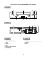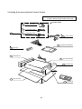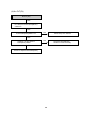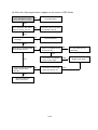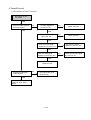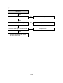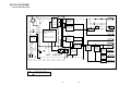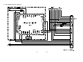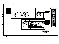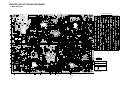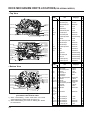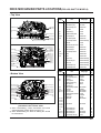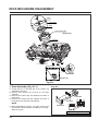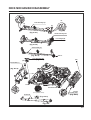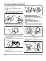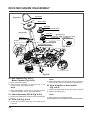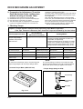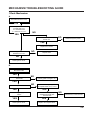
1
VIDEO CASSETTE RECORDER
VHR-M261EV,VHR-M261SP
VHR-M291E,VHR-M291EV,VHR-M291IR
INDEX
1. SUMMARY
CABINET & MAIN CHASIS
ELECTRICAL (ADJUSTMENT)
ELECTRICAL (TROUBLESHOOTING)
ELECTRICAL (BLOCK DIAGEAMS)
2. ELECTRICAL (CIRCUIT DIAGEAMS 1)
3. ELECTRICAL (CIRCUIT DIAGEAMS 2)
4. ELECTRICAL (PRINTED CIRCUIT BOARD 1)
5. ELECTRICAL (PRINTED CIRCUIT BOARD 2)
6. MECHANISM (PARTS LOCATIONS)
MECHANISM (DISASSEMBLY 1)
7. MECHANISM (DISASSEMBLY 2)
8. MECHANISM (DISASSEMBLY 3)
9. MECHANISM (ADJUSTMENT)
A. MECHANISM (MAIN TENACE/
INSPECTION PROCDURE)
MECHANISM (TROUBLESHOOTING)
B. MECHANISM (EXPLODED VIEWS)
C. REPLACEMENT PAETS LIST
I
i n d ex
FILE NO.
SERVICE MANUAL
Video Cassette Recorder
VHR-M261EV
(Product Code : 143 182 15)
(Europe)
VHR-M271SP
(Product Code : 143 182 16)
(Spain, Portugal)
VHR-M291E
(Product Code : 143 182 12)
(U.K.)
VHR-M291EV
(Product Code : 143 182 14)
(Europe)
(VHR-M291EV)
VHR-M291IR
(Product Code : 143 182 13)
(Ireland)
Feb./ '01/ 4320 K
SANYO Electric Co.,Ltd.
Osaka, Japan
KR2LN/EV2, SP, E, EV, IR
REFERENCE No.SM5310270
I
i n d ex
REFERENCE
MODEL NUMBER DECODER
FRONT
REAR
VHR-M291E
NO
NO
2SCART
VHR-M291IR
NO
NO
2SCART
VHR-M271SP
CANAL
NO
2SCART
VHR-M261EV
NO
NO
1SCART
VHR-M291EV
NO
NO
1SCART
TABLE OF CONTENTS
BLOCK DIAGRAMS . . . . . . . . . . . . . . . . . . . . .3-17
SECTION 1
SUMMARY
1. Power Block Diagram . . . . . . . . . . . . . . . . . . . .3-17
2. Tuner/IF, NICAM & A2 Block Diagram . . . . . . . .3-19
3. Y/C Block Diagram . . . . . . . . . . . . . . . . . . . . . .3-21
KEY TO ABBREVIATIONS . . . . . . . . . . . . . . . . 1-1
IMPORTANT SAFETY PRECAUTIONS . . . . . . . . . . 1-2
• Precautions During Servicing
SAFETY CHECK AFTER SERVICING . . . . . . . . 1-3
4. System Block Diagram . . . . . . . . . . . . . . . . . . .3-23
5. AUDIO Block Diagram . . . . . . . . . . . . . . . . . . . .3-25
6. SCART Block Diagram . . . . . . . . . . . . . . . . . . .3-27
CIRCUIT DIAGRAMS . . . . . . . . . . . . . . . . . . . .3-29
• Insulation resistance test
1. Power, Tuner, NICAM/A2 Circuit Diagram . . . . .3-29
• Dielectric strength test
2. A/V, SECAM, VPS Circuit Diagram . . . . . . . . . .3-32
• Clearance distance
3. System Circuit Diagram . . . . . . . . . . . . . . . . . . .3-35
• Leakage current test
PROPOSAL FOR APPLYING SHORT
PROTECTION . . . . . . . . . . . . . . . . . . . . . . . . . . .1-4
PROPOSAL FOR APPLYING SHORT
SERVICE NOTICE ON REPLACING EEPROM . .1-5
SPECIFICATIONS . . . . . . . . . . . . . . . . . . . . . . . 1-6
LOCATION OF CUSTOMER CONTROLS . . . . . 1-7
SECTION 2
CABINET & MAIN CHASSIS
4. SCART Circuit Diagram . . . . . . . . . . . . . . . . . . .3-37
PRINTED CIRCUIT BOARD DIAGRAMS . . . . .3-39
1. MAIN P.C.Board . . . . . . . . . . . . . . . . . . . . . . . .3-39
2. KEY 1 P.C.Board . . . . . . . . . . . . . . . . . . . . . . . .3-41
3. KEY 2 P.C.Board . . . . . . . . . . . . . . . . . . . . . . . .3-42
SECTION 4
MECHANISM
NOTE) The table of contents for this section is edited
NOTE) separately.
SERVICE METHOD . . . . . . . . . . . . . . . . . . . . . 2-1
Electrical Part . . . . . . . . . . . . . . . . . . . . . . . . . . . . . 2-1
EXPLODED VIEWS . . . . . . . . . . . . . . . . . . . . . . 2-2
1. Cabinet & Main Frame Section . . . . . . . . . . . . . 2-2
2. Packing & Accessory Remote Control Section . . 2-3
SECTION 5
REPLACEMENT PARTS LIST
• Mechanical Section . . . . . . . . . . . . . . . . . . . . . . . .5-1
SECTION 3
ELECTRICAL
ELECTRICAL ADJUSTMENT POINTS
ARRANGEMENT . . . . . . . . . . . . . . . . . . . . . . . .3-1
ELECTRICAL ADJUSTMENT PROCEDURES . . 3-2
1. Servo Circuit . . . . . . . . . . . . . . . . . . . . . . . . . . . 3-2
ELECTRICAL TROUBLESHOOTING GUIDE . . . 3-3
1. Power Circuit(SMPS) . . . . . . . . . . . . . . . . . . . . . 3-3
2. Servo Circuit
. . . . . . . . . . . . . . . . . . . . . . . . . . .3-6
3. System & Front Panel Circuit . . . . . . . . . . . . . . . .3-9
4. Y/C Circuit . . . . . . . . . . . . . . . . . . . . . . . . . . . . .3-11
5. Tuner/IF Circuit . . . . . . . . . . . . . . . . . . . . . . . . .3-15
• Electrical Section . . . . . . . . . . . . . . . . . . . . . . . . .5-4
SECTION1 SUMMARY
KEY TO ABBREVIATIONS
A
B
C
AC
ACC
ACSS
ADJ
A/E
AFC
AFT
AGC
A.H.SW
ALC
AM
AMP
ANT
APC
ASS’Y
AUX
B
BGP
BPF
BS
BW or B/W
C
CAN
CAP
CAP.BRK
CAP.RVS
CATV
CBA
CCD
C.CTL
CFG
CHROMA
CNR
COMB
COMP
D
E
F
G
H
I
L
CONV
C.ROT SW
CS
C.SYNC
CTL DIV
CUR
CYL
D
D.ADJ
DC
D.CTL
DEMOD
DET
DEV
DHP
DIGITRON
DL
DOC
DUB
D.V SYNC
E
EE
EMPH
ENA
ENV
EP
EQ
EXP
F
FB
FBC
FE
FG
FL
FM
F/R
FS
FSC
F/V
GEN
H
IC
IF
INS
L
LD
LD VTG CTL
LECHA
L.M
LP
:Alternating Current
:Automatic Color Control
:Automatic Channel Setting System
:Adjust
:Audio Erase
:Automatic Frequency Control
:Automatic Fine Tuning
:Automatic Gain Control
:Audio Head Switch
:Automatic Level Control
:Amplitude Modulation
:Amplifier
:Antenna
:Automatic Phase Control
:Assembly
:Auxiliary
:Base
:Burst Gate Pulse
:Bandpass Filter
:Brodcasting Satellite
:Black and White
:Capacitor, Chroma, Collector
:Cancel
:Capstan
:Capstan Brake
:Capstan Reverse
:Cable Television
:Circuit Board Assembly
:Charge Coupled Device
:Chro Control, Capstan Control
:Capstan Frequency Generator
:Chrominance
:Chroma Noise Redution
:Combination
Comb Filter
:Comparator
Composite
Compensation
:Converter
:Color Rotary Switch
:Chip Selcet
:Composite Synchronization
:Control Divide
:Current
:Cylinder
:Drum, Digital, Diode, Drain
:Drum Adjust
:Direct Current
:Drum Control
:Demodulator
:Detector
:Deviation
:Double High Pass
:Digital Display Tube
:Delay line
:Drop Out Compensator
:Dubbing
:Dummy Vertical Synchronization
:Emitter
:Electric to Eletric
:Emphasis
:Enable
:Envelope
:Extended Play
:Equalizer
:Expander
:Fuse
:Feed Back
:Feed Back Clamp
:Full Erase
:Frequency Generator
:Filter
:Frequency Modulation
:Front/Rear
:Frequency Synthesizer
:Subcarrier Frequency
:Frequency Voltage
:Generator
:High, Horizontal
:Integrated Circuit
:Intermediate Frequency
:Insert
:Low, Left, Coil
:LED
:Loading Voltage Control
:Letter Character
:Level Meter
:Long Play
M
N
O
P
Q
R
S
T
U
V
W
X
Y
Z
1-1
LPF
MAX
MD
MECHA.CTL
MIC
MIN
MIX
M.M.
MMV
MOD
MODEM
MPX
NR
:Low Pass Filter
:Maximum
:Modulator
:Mechanism Control
:Microphone
:Minimum
:Mixer, Mixing
:Monostable, Multivibrator
:Mono Multi Vibrator
:Modulation, Modulator
:Modulator-Demodulator
:Multiplex
:Noise Reduction
OSC
OSD
PB
PCB
P.CTL
PRE-AMP
P.F
PG
PLL
PREM.DET
P.P
PS
PWM
PWR CTL
Q
QH
QSR
QTR
QV
R
RE(or RC)
REC
REC S ‘H’
REF
REG
REMOCON
RF
R/P
RTC
S
S.ACCEL
SAOP
SC
S.DET
SH
SHARP
SIF
SLD
S/N
SP
ST
SUB
SW or S/W
SYNC
SYSCON
T
TP
TR
TRK
TRANS
TU
UHF
UNREG
V
VA
VCO
VGC
VHF
V.H.SW
VISS
VPS
VR
V-SYNC
VTG
VV
VXO
W
WHT
W/O
X-TAL
Y/C
YNR
ZD
:Oscillator
:On Screen Display
:Playback
:Printed Circuit Board
:Power Control
:Preamplifier
:Power Failure
:Pulse Generator
:Phase Locked Loop
:Premire Detect
:Peak-to-Peak
:Phase Shift
:Pulse Width Modulation
:Power Control
:Transistor
:Quasi Horizontal
:Quick Setting Record
:Quick Timer Record
:Quasi Vertical
:Resistor, Right
:Remocon, Receiver
:Recording
:Record Start ‘Hight’
:Reference
:Regulated, Regulator
:Remote Control(unit)
:Radio Frequency
:Record/Playback
:Reel Time Counter
:Serial
:Slow Accel
:Second Audio Program
:Scart, Simulcast
:Secam Detect
:Shift
:Sharpness
:Sound Intermediate Frequency
:Side Locking
:Signal to Noise Ratio
:Standard Play
:Stereo
:Subtract, Subcarrier
:Switch
:Synchronization
:System Control
:Coil
:Test Point
:Transistor
:Tracking
:Transformer
:Tuner, Take-up
:Ultra High Frequency
:Unregulated
:Volt, Vertical
:Always Voltage
:Voltage Controlled Oscillator
:Voltage Gain Control
:Very High Frequency
:Video Head Switch
:VHS Index Search
:Video Program System
:Variable Resistor or Volume
:Vertical Synchronization
:Voltage
:Voltage to Voltage
:Voltage X-tal Oscillator
:Watt
:White
:With out
:Crystal
:Luminance/Chrominance
:Luminance Noise Reduction
:Zener Diode
IMPORTANT SAFETY PRECAUTIONS
Prior to shipment from the factory, the products are strictly inspected to confrom with the recognized product
safety and electrical codes of the countries in which they are to be sold. However, in order to maintain such compliance, it is equally important to implement the following precautions when a set is being serviced.
• Precautions during Servicing
1. Locations requiring special caution are denoted by labels and inscriptions on the cabinet, chassis and
certain parts of the product. When performing service, be sure to read and comply with these and other
cautionary notices appearing in the operation and service manuals.
2. Parts identified by the
symbol and shaded ( Y ) parts are critical for safety.
Replace only with specified part numbers.
Note : Parts in this category also include those specified to comply with X-ray emission standards for
products using cathode ray tubes and those specified for compliance with various regulations
regarding spurious radiation emission.
3. Use Specified internal wiring. Note especially:
1) Double insulated wires
2) High voltage leads
4. Use specified insulating materials for hazardous live parts. Note especially:
1) Insulation Tape
2) PVC tubing
3) Spacers
4) Insulation sheets for transistor
5. Observe that wires do not contact heat producing
parts (heatsinks, oxide metal film resistors, fusible
resistors, etc.)
6. Check that replaced wires do not contact sharp edged
or pointed parts.
7. 1) When a power cord has been replaced, check
that A mark is made on the cord, under strain,
near the aperture, and the flexible cord is
subjected 100 times to a pull of 40N for a duration
of 1 second each.
2) During the test, the cord shall not be displaced by
more than 2mm
Power code
Fig. 1
8. Also check areas surrounding repaired locations.
9. The internal wiring is secured so as not to approach the heating parts and high voltage parts by its shape.
So, these wires must be restored to its former state.
1-2
SAFETY CHECK AFTER SERVICING
Examine the area surrounding the repaired location for damage or deterioration. Observe that screws, parts and
wires have been returned to original positions. Afterwards, perform the following tests and confirm the specified
values in order to verify compliance with safety standards.
• Insulation resistance test
confirm the specified insulation resistance or greater between power cord plug prongs and externally exposed
parts of the set (RF terminals, antenna terminals, video and audio input and output terminals, incrophone jacks,
earphone jacks, etc.) See table below.
• Dielectric strength test
Confirm specified dielectric strength or greater between power cord prongs and exposed accessible parts of
the set (RF terminals, antenna terminals, video and
audio input and output terminals, incrophone jacks,
earphone jacks, etc.) See table below.
d
Primary circuit terminals
• Clearance distance
Chassis
When replacing primary circuit components, confirm
specified clearance distance (d), (d') between soldered terminals, and between terminals and surrounding metallic parts. See table below.
a
Fig. 2
Table 1 : Ratings for selected areas
AC Line Voltage
Region
Insulation
Resistance
Dielectric
Strength
Clearance
Distance(d),(d)
F 6mm(d)
*100 to 130 V
Europe
F 8mm(d)
F 10 MΩ/500 V DC
4kV
1
minute
*200 to 240 V
Australia
(a Power cord)
* Class II model only.
Note. This table is unofficial and for reference only. Be sure to confirm the precise values for your particular
country and locality.
• Leakage Current test
Confirm specified or lower leakage current between B(earth ground, power cord plug prongs) and externally
exposed accessible parts (RF terminals, antenna terminals, video and audio input and output terminals, microphone jacks, earphone jacks, etc.)
Exposde
accessible
part
Load
Measuring Method: (Power ON)
Insert load Z between B(earth ground, power cord
plug prongs) and exposed accessible parts. Use an
AC voltmeter to measure across both terminals of
load Z. See figure and following table.
Region
AC Voltmeter
Earth Ground,
Power cord plug prongs
B
Table 2:Leakage current ratings for selected areas.
AC Line Voltage
Z
Load Z
Fig. 3
Leakage Current(i)
Earth Ground
(B) to :
i E 0.7m A peak
Antenna earth
terminals
i E 2m A DC
i E 0.7m A peak
200 to 240 V
Australia
Other terminals
i E 2m A DC
50kΩ
Note. This table is for IEC member only. Be sure to confirm the precise values for your particular country and
Note. locality.
100 to 130 V
Europe
2kΩ
1-3
PROPOSAL FOR APPLYING SHORT PROTECTION
• The Contents of Examination
As all the IC that is applied to VCR is controlled by IIC, mutual communication, if Vcc of IC is short or open
with detecting ‘Acknowledge’ data of the specific IC according to each power(5V, 5VT) µ-COM gets unable to
detect ‘ACK’ data.
µ-COM regards this case as abnormal one and if it can’t detect ‘ACK’ data for a certain time(3.5 sec) the signal of ‘Power Control’ and ‘Timer Control’ are switched to ‘Low’. As a result POWER Switching TR is kept from
generating heat and fire.
Conception
BLOCK Diagram
TIMER
CONTROL
5VT SW
SLAVE with 5V
IIC BUS
MASTER
SLAVE with 5V
POWER
CONTROL
5VT SW
• POWER for each IC
5.2V
5.2VT
Modulator
5.3VA
Hi-Fi IC
5.3VA
NICAM IC
Power Control
AVCP IC
TUNER
OSD
VPS IC
SECAM IC
Timer Control
• IC to detect ‘ACK’ data is selected as below because IC is different in accordance to region and option
S/
Series
P/Y/I
Series
5V POWER
5VT POWER
5V POWER
5VT POWER
SECAM IC
AVCP IC
Modulator
AVCP IC
*Short protection off mode : DJ01 Diode in
1-4
SERVICE NOTICE ON REPLACING EEPROM
In case that defective EEPROM of PAL models is replaced, to operate these sets from the initial state MP KEY
must be repaired as well before delivering to the customer.
If MP KEY isn’t repaired the setting of RF OUT channel or LANGUAGE might be different from that for custormer’s country.
•MP KEY : In case of PAL VCR if holding the REC button on the front panel and the CLEAR button on the
remote control handset for 5 ~ 7 seconds with power being switch all and no tapes,
OK is displayed at FLD for FLD models and LED becomes on for LED CLOCK models.
This is the state that initializing EEPROM is finished.
(In case of PAL VCP if holding the REC button on the front panel and the MENU button on the
remote control handset for 5 ~ 7 seconds with power being off and no tapes, All the LED DOTs
become on. This is the state that initializing EEPROM is finished.)
•MP KEY's function : MP KEY sets EEPROM's data up to the initial state.
• FLD MODEL:
MP KEY “OK”
OK
REC
VCR
TIMER
• LED CLOCK MODEL:
MP KEY Switch all on a Light
AM
• LED DOT MODEL:
MP KEY Switch all on a Light
1-5
SPECIFICATIONS
General
Power
Power consumption
Video Head system
Tape speed
Tape format
Maximum recording time
Rewind time
Dimensions (W X H X D)
Weight
Operating temperature
Operating humidity
Timer
Video
Television system
Recording format
RF Out
RF Modulator
Input level
Output level
Signal to noise ratio
Audio
Input level
Output level
Audio track
Audio signal to noise ratio
: 200~240V, 50Hz
: Approx. 14 watts(Energy Saving mode : 3 watts)
: Rotary 2 heads, helical scanning system
: PAL/MESECAM : 23.39 mm/s (SP mode)
11.69 mm/s (LP mode)
NTSC (Playback only) : 33.35 mm/s (SP mode)
16.67 mm/s (LP mode)
11.12 mm/s (EP mode)
: Tape width 1/2” (12.7 mm high density VHS tape)
: 4 hours in SP mode/8 hours in LP mode (with E-240 tape)
: Approx. 150 sec. (with E-180 tape)
: 14.2” X 3.6” X 11.4” (360 x 94 x 270 mm)
: 9.0 lbs. (4.0 kg)
: 41°F-95°F (5°C-35°C)
: Less than 80%
: 24 hours display type
: CCIR standard (625 lines, 50 fields)
PAL(B/G) colour signal(VHR-M271SP/M261EV/M291EV)
PAL(I) colour signal(VHR-M291E)
PAL(I/I) colour signal(VHR-M291IR)
: PAL
: G(VHR-M271SP/M261EV/M291EV)
I (VHR-M291E/M291IR)
: UHF 22-68 (Adjustable)
: VIDEO IN (SCART type)
1.0 Vp-p, 75 ohm, unbalanced
: VIDEO OUT (SCART type)
1.0 Vp-p, 75 ohm, unbalanced
: More than 43 dBm
: AUDIO IN (SCART type)
-3.8dBm, more than 10kΩ
: AUDIO OUT (SCART type)
-3.8dBm, less than 1kΩ
Mono track
: More than 43 dBm(at SP mode)
• Design and specifications are subject to change without notice.
1-6
LOCATION OF CUSTOMER CONTROLS
FRONT
1
2
3
11
10
4
9
8
5
6
7
REAR
1
2
FRONT
11.
12.
13.
14.
15.
16.
17.
18.
19.
10.
11.
POWER
STOP & TAPE EJECT
CASSETTE COMPARTMENT
REW
PAUSE
FAST FORWARD
PLAY
REC
REMOTE CONTROL SENSOR
VCR DISPLAY
CHANNEL(-/+)
3
4
5
REAR
11. MAINS LEAD
12. EURO AV2
(VHR-M271SP, VHR-M291IR,VHR-M291E ONLY)
13. EURO AV1
14. RF.OUT
1-7
REMOTE CONTROL
NUMBER buttons
1
2
POWER button
3
TV/VCR
4
5
TV/VCR button
6
CM-CUT
7
8
SAFE button
CM-CUT button
9
INPUT
SAFE
SP/LP
SP/LP button
0
REC
EJECT
EJECT button
PAUSE button
REW button
REC button
PAUSE
REW
PLAY
STOP button
FF
FF button
PLAY button
STOP
OK
i
CLK/COUNT
i button
VIDEO Plus+ button
VHR-M291E/VHR-M291IR/VHR-M291EV ONLY
CH
TRACK
CURSORS button
CLEAR
OK/CLK/COUNT button
CLEAR button
B30902
1-8
SECTION 2 CABINET & MAIN CHASSIS
SERVICE METHOD
Electrical Part
(1) Re-assembly Flow for service like Fig. 2-1
Timer C.B.A
Main C.B.A
Housing & Deck
Assembly
(2) To check and replace Electrical parts
2 Re-assemble the unit according to No.1) Re-assembly Flow.
3 Place the unit like Fig. 2-1
4 Check and replace Electrical parts.
NOTE :
1 Insert Video Cassette Tape inversely like Fig. 2-1 to check and replace defective parts.
2 In disassembling and reassembling, be careful not to damaged CST switch.
(Positioned Upside Down)
Main C.B.A
Cassette Tape
(Upside Down)
Housing & Deck Ass'y
Timer C.B.A
Fig.2-1
2-1
EXPLODED VIEWS
1. Cabinet and Main Frame Section
452
A46
LED502(LED501)
TU70
323
1(TU
NER
)
1SCART
452
452
2SCART
462
320
300
5
NOTE) Refer to “SECTION 5 REPLACEMENT
PARTS LIST” in order to look for the
part number of each part.
_ OPTIONAL PARTS
330
A43
283
A42
A00
280
284
457 457
457
2
457
457
457
260
A49
452
3
250
462
275
4
1
A
B
C
2-2
D
2.Packing & Accessory Remote Control Section
NOTE) Refer to “SECTION REPLACEMENT PARTS LIST
NOTE) in order to look for the part number of each part.
OPTIONAL PARTS
806
811
810
812
CABLE SET ASS'Y
(Optional parts)
PLUG ASS'Y 1WAY
(Optional parts)
PLUG ASS'Y 2WAY
(Optional parts)
821
801
808
BATTERY
803
PACKING (LF)
SCART CABLE
INSTRUCTION MANUAL
804
BAG. SOFR SHEET
803
802
PACKING (RF)
BOX CARTON
900
2-3
REMOCON
SECTION 3 ELECTRICAL
ELECTRICAL ADJUSTMENT POINTS ARRANGEMENT
: Measurement point
: Adjustment point
SCART JACK
VPS
S
M
P
S
Drum
Connector
Hi-Fi
OSC
C+
AVCP
T
U
N
E
R
Secam
A/V
W5J5
H
S
R
Micom
SYSTEM
NICAM
W5J4
H/SW
PG.ADJ
L/D IC
E2PROM
DISPLAY(DOT,CLK)
KEY-BOARD 2
KEY-BOARD 1
MAIN P.C.B
(Component Side)
3-1
ELECTRICAL ADJUSTMENT PROCEDURES
1. Servo Adjustment
1) PG Adjustment
• Test Equipment
a) OSCILLOSCOPE
b) PAL TEST TAPE (VHS SP)
• Adjustment And Specification
MODE
MEASUREMENT POINT
ADJUSTMENT POINT
SPECIFICATION
PLAY
V.Out
H/SW(W5J4, W5J5)
VR501
6.5 ± 0.5H
• Adjustment Procedure
a) Insert the PAL SP Test Tape and play.
Note - Adjust the distance of X, pressing the Tracking(+) or Tracking(-) when the “ATR” is blink after the
PAL SP Test Tape is inserted.
b) Connect the CH1 of the oscilloscope to the H/SW(W5J4, W5J5) and CH2 to the Video Out for the VCR.
c) Trigger the mixed Video Signal of CH2 to the CH1 H/SW(W5J4, W5J5), and then check the distance
(time difference), which is from the selected A(B) Head point of the H/SW(W5J4, W5J5) signal to the
starting point of the vertical synchronized signal, to 6.5H ± 0.5H (416µs, 1H=64.0µs).
• CONNECTION
V.Out
OSCILLOSCOPE
CH1 CH2
H/SW(W5J4,W5J5)
VR501
H/SW V.out
(W5J4, W5J5)
• WAVEFORM
H/SW
6.5H(416us)
Composite
VIDEO
3-2
ELECTRICAL TROUBLESHOOTING GUIDE
1. Power Circuit(SMPS)
(1) No 5.3VA.
No 5.3VA.
YES
Is the F101 normal?
NO
Replace the F101
(Use the same Fuse).
YES
Is the BD101 normal?
NO
Replace the BD101.
YES
Is the R101 normal?
NO
Replace the R101.
YES
Does the oscillation waveform appear at
the IC101 Pin 1?
NO
Is Vcc(about 13~15V) permittable at the
IC101 Pin 4?
NO
YES
Check or Replace the D103.
Is there DC voltage at the IC101 Pin 5?
NO
Replace the IC102.
YES
Is there about 2.5V at the IC103 Vref ?
NO
Replace the IC103.
YES
Is the D106 normal?
NO
YES
Check the Main PCB 5.3VA Line short?
3-3
Replace the D106.
7. Power Circuit(SMPS)
(2) No 12VA.(Capstan)
No 12VA.
YES
Does 5.3VA work normally?
NO
Check whether 5.3VA is out of order.
YES
Is the D109 normal?
NO
Replace the D109.
YES
Check 12VA Line of the Main PCB short.
(3) No 12VA (CANAL, Buffer)
No 12VA.
YES
Is Vcc(about 13VA) put into the D160(+)?
NO
YES
Is Voltage(about 12V) put into the D160(-)?
YES
Check or Replace the D160.
3-4
Replace the Peripheral Circuitry of D160.
7. Power Circuit(SMPS)
(4) No 5VT(5V)
No 5VT.(5V)
YES
Is 5.3VA put into the Q152(Q151)
collector?
YES
Is the Q163(Q162) Base “H”?
NO
Check the µ-com Control.
YES
Is about 4.7V put into the
Q152(Q151) Base?
NO
YES
Check or Replace the Q152(Q151).
3-5
Check the Q163(Q162)
whether it works normally.
2. Servo Circuit
A.
Unstable Video in PB
Mode.
Does the on screen noise
level change periodically?
YES
Do CTL pulses appear at
IC501 pin 37?
YES
NO
Does the CFG divide
waveform appear at IC501
pin 40?
Is the height of the CTL
Head adjusted correctly?
NO
YES
Do the CTL pulses move
when TRK is operated?
YES
Adjust the CTL Head.
NO
Does the Video Envelope
waveform appear at IC501
Pin 12?
YES
Replace IC501.
Replace IC501.
NO
Check AVCP IC.
3-6
B.
Drum Motor stopped.
Does 12V appear at PMD01 Pin 4?
NO
YES
Does 2.8V appear at PMD01 Pin 1?
Check Power.
NO
Check Connector and Drum Motor Ass’y.
Does Drum PWM appear at IC501 Pin 26?
NO
YES
Check the Components and foil Pattern
between IC501 Pin 26 and PMD01
Pin 1 for shorts.
Do DFG Pulses appear at PMD01 Pin 3?
NO
YES
Do DFG Pulses appear at IC501 Pin 38?
YES
Check Drum Monitor Ass’y.
NO
Check the Components and foil pattern
between PMD01 Pin 3 and IC501
Pin 38 for shorts.
Does the Drum PWM waveform
appear at IC501 Pin 26?
YES
NO
Check the Components and foil Pattern
Connected to IC501 Pin 26 PMD01
Pin 1 for shorts.
Replace IC501.
3-7
C.
Capstan Motor Stopped.
Does 12VA appear at PMC01 Pin 5?
NO
YES
Does 2.8V appear at PMC01 Pin 4?
Check Power.
NO
YES
Check Connector and Capstan
Motor Ass’y.
Does PWM wave appear at IC501
Pin 25?
NO
YES
Check the Components and foil Patterns
Connected between IC501 Pin 25 and
PMC01 Pin 4 for shorts.
Does the CFG signal appear at PMC01
Pin 6?
NO
YES
Does the CFG signal appear at IC501
Pin 40?
YES
Check Capstan Motor Ass’y.
NO
Check Components and foil patterns
between PMC01 Pin 6 and IC501
Pin 40 for shorts.
Does Capstan PWM appear at IC501
Pin 25?
YES
NO
Check the components and foil pattern
connected between IC501 Pin 25 and
PMC01 Pin 4 for shorts
Replace IC501.
3-8
3. System & Front Panel Circuit
A.
Auto stop.
Does SW30 waveform
appear at IC501 Pin 24?
YES
NO
Do Take-up reel pulses
appear at IC501 Pin 4?
YES
Check the Drum Motor
Signal.
NO
Do Take-up reel pulses
appear at the base of
Q514?
Change IC501.
NO
YES
Does 5.3V appear at
RS501.
YES
Replace the Take-Up Reel
Photocoupler in the
Deck(RS501).
3-9
NO
Check the Power.
B.
Cassette tape loading is unstable.
Is REG 12V applied to IC502 Pin 6?
YES
NO
Is High signal applied to IC501 Pin 57
when inserting the CST?
Check the power.
NO
Is 5.3V applied to R544?
YES
YES
Does Low signal occur form IC501 Pin 19
when inserting the CST?
YES
Check the CST SW and
peripheral circuitry.
Check the power.
NO
Does 6.2V occur from IC502 Pin 2 when
inserting the CST?
YES
NO
Check IC501 Pins 74, 75, 76, 77.
NO
Check the Deck Mechanism.
Change IC502 or ZD501(GDZJ 6.2C).
NOTE : Auto stop may also be caused by lack of lubrication,due to dried grease or oil.
C.
Non working finction buttons.
Is the voltage of IC501 Pin 15, 5V?
YES
NO
Does(LED CLOCK) display change
when a function button is pressed?
YES
Check the power.
NO
Replace the defective Switch.
(Function SW)
Replace IC501.
3-10
4. Y/C CIRCUIT
(1) No Video in EE Mode,
No Video in EE Mode
Does the Video signal
appear at the IC301 Pin 38?
NO
Check the Video Input
Jack.
(Line In Jack)
YES
NO
Is 5V applied to the IC301
Pins 16, 40, 55, 58, 75, 87?
Check the 5V Line.
(Power Circuit)
YES
Does the Video signal
appear at the IC301 Pin 29?
NO
Is I2C BUS signal applied to
the IC301 Pin 23, 24?
YES
Does the Video signal
appear at the IC501 Pin 45?
NO
YES
NO
Chck the path of the signal
between the IC301 Pin 29
and IC501 Pin 43.
Check C316. (AGC)
YES
YES
Does the Video signal
appear at the Emitter
terminal of the Q701?
Check the System Circuit.
(Refer to ‘SYSTEM I2C BUS
CHECK Trouble Shooting’)
NO
Does the 5V appear at
the Emitter terminal of
the Q701.
NO
Replace the IC301.
YES
Replace the Q701.
3-11
Check the 5V Line.
(Power Circuit)
3. Y/C CIRCUIT
(2) When the Y(Luminance) signal doesn’t appear on the screen in PB Mode,
Is 5V applied to the IC301
Pins 16, 40, 55, 58, 87?
NO
Check the line of the 5.2V
Line. (Power Circuit)
YES
Is the I2C Bus siganl applied NO
to the IC301 Pins 23, 24?
Refer to ‘SYSTEM I2C BUS
CHECK Trouble Shooting’.
YES
NO
Does the normal RF signal
appear at the IC301 Pin 74?
NO
Is the V.H.S/W signal
applied to the IC301 Pin 11 ?
Check the System Circuit.
(IC501 Pin 24)
YES
Is V.H.S/W “H” about 3.4V
at the IC301 Pin 11?
NO
Check the V.H.S/W level.
(Check R304, R340)
YES
YES
Clean the Drum.
Does the Y(Luminance) RF NO
signal appear at the IC301
Pin 17?
NO
Check the path of the
Y(Luminance) RF signal.
(Check the Q301)
YES
Check the path of the
Y(Luminance) RF signal.
(Check Q302, Q303)
YES
YES
Is the Y(Luminance) Video
waveform showed up at
theIC301 Pin 41?
NO
YES
Replace the IC301.
3-12
Replace the IC301.
3. Y/C CIRCUIT
(3) When the C(Color) signal doesn’t appear on the screen in PB Mode,
Is 5V applied to the IC301
Pins 16, 40, 55, 58, 87?
NO
Check the line of the 5.2V
Line. (Power Circuit)
NO
Check the Color Rotary
Circuit. (IC501 pin 28 )
YES
Is the Color Rotary signal
applied to the IC301
Pin 10?
YES
Is Color Rotary “H”
about 1.6V?
Check the Color Rotary
level.
(Check the R303)
NO
YES
Does the Color signal
appear at the IC301
Pin 71 ?
YES
Replace the IC301.
NO
NO
Does the X301(4.43MHZ)
or X302(3.58MHZ) oscillate?
Replace the X301 or
the X302.
NO
Does the Color signal
appear at the IC301 Pin 61?
Check the Color Pass.
(Check the Q304)
Check the circuit of the
IC301 35, 62.
3-13
YES
Replace the IC301.
3. Y/C CIRCUIT
(4) When the Video signal doesn’t appear on the screen in REC Mode,
Is the EE signal normal?
NO
Check EE Mode.
YES
Is 5V applied to the IC301
Pins 16, 40, 55, 58, 87?
NO
Check the line of the 5.2V
Line.(Power Circuit)
YES
Does PB Mdoe operate
normally?
NO
Check PB Mode.
YES
Does the RF signal appear
at the IC301 Pin 12?
NO
Is the REC ‘H’ signal
(about 4V) applied to the
IC 301 Pin 30?
NO
Check the System of REC
‘H’. (the IC501 Pin 79
/ the D301)
YES
YES
Does the REC RF signal
appear at the IC301
Pin 90?
NO
Check REC Luminance
Pass & Color Pass.
YES
Check the circuit of the
IC301 Pin 90, 92, 94.
YES
YES
Check the Drum &
Drum Connector
3-14
Replace the IC301.
5. Tuner/IF circuit
(1) No picture on the TV screen
No picture on the
TV screen
YES
Does the Video signal at
the TU701 Pin24?
NO
Is +30VT applied to
TU701 Pin 16?
YES
NO
Check 33VT line.
YES
Is +5VT applied to
TU701 Pin 13?
NO
Check 5VT line.
YES
Does the Clock signal
appear at TU701 Pin 11?
NO
Check the liC Clock
signal of µ-com Pin 90.
NO
Check the liC Data signal
of µ-com Pin 91.
YES
Does the data signal
appear at TU701 Pin 12?
YES
Replace Tuner
Does Sync appear at
IC501 Pin54?
NO
Check the signal flow
from TU701 Pin 24 to
IC301 Pin 38.
YES
Check the signal flow from
IC501 Pin45 to JK901
Pin19.
3-15
(2) No sound
No sound
YES
Check the Vcc of IC301 Pin 75.
NO
Check 5VT power.
YES
Check the Tuner Audio signal
at IC301 Pin 76.
NO
Chekc the signal flow from TU701
Pin21 to IC301 Pin 76.
YES
Check the Audio signal at IC301 Pin 96.
NO
YES
Check the signal flow from IC301
pin 96 to IC901 Pin 6.
3-16
Replace IC301.
BLOCK DIAGRAMS
1. Power Block Diagram
BD101
!
T101 !
TRANSFORMER
R101
4
2
6
SNUBBER
BLOCK
1
+
3
7
C103
8
(D102,R104,
C105,C106)
RECTIFIER
& SMOOTHING
R115
(D109, C120,
L104,C121)
TO Canal+
12VA
D160
D151
4
9
RECTIFIER
& SMOOTHING
24V S/W
Q159,R166,R167
(D110, C123)
R106
F. µ-com
SEARCH "H"
Q161
R163
TO CAPSTAN M
24/12VA
DRIVE & S/W BLOCK
OVER CURRENT LIMIT
BLOCK
R102
LINE FILTER
BLOCK
(IC101, R109, C135, D103,
10
R103,C109, R125, R126)
(C101,L102,
C102)
TO DRUM
12VA
RECTIFIER
& SMOOTHING
D152
(D106, C116,
L103,C117)
3
TO TU/IF
33V
11
!
2
RECTIFIER
& SMOOTHING
12
F101
(D105, C115)
!
HOT GND
1
4
!
C113
C112
FEED-BACK
BLOCK
!
3
IC102
BK
WH
(BR)
(BL)
PW101
!
2
!
HOT CIRCUIT
TO SYS, TU/IF
5.4VA
36V S/W
BLOCK
(Q154, R157,
R158,R155)
TO AV, TU/IF,
SECAM, VPS
5.2VT
5VT SW
BLOCK
(Q152, R153,
R154, D156)
5V S/W
BLOCK
(Q151, R151,
R152)
(R116,R117,R118
R119,R120,R121
C114)
PWR CTL
BLOCK
IC103
(Q162, R161)
Q163
TO Hi-Fi, Sensor
5.2V
FROM µ-COM
P.CTL"H"
TIMER "H"
FROM µ-COM
'00 11. 30
NOTES :
Symbol denotes AC ground.
Symbol denotes DC chassis ground.
3-17
3-18
(From Power)
2. Tu/IF, NICAM & A2 Block Diagram
WITHOUT
3-19
3-20
3. Y/C Block Diagram
1) PB Mode
2) REC Mode
PB
RF
15
74
57
59
52
54
51
61
72
21
71
71
IC201 TA1238F
ACC
MAIN
CONV
C. COMB
LPF
Y
DELAY
C LPF
SP 'B' PB
SP 'A' PB
V. ENV
11
18
COMB
AMP
DOUBLE
LIMIT
17
57
59
C. COMB
CCD
LPF
NL
DE EMP
90
(TO DRUM)
Y/C
MIX
46
Y
DELAY
15
IC201
TA1238F
24
45
43
YNR
+
CLAMP
20
DETAIL
ENH
Y-LPF
NL EMPH
FBC
FM
MOD
60dB AMP
23
24
28
V. IN 3
34
36
38
REC FM
EQ
LPF
V. IN 2
V. IN 1
S/W
32
W/D
CLIP
AGC
31
S/W V.OUT
29
10
PB
PEAKING
54
41
SUB
LPF
21
52
BPF1
FM
DEM
93
10
45
51
SP REC
YNR
PB EQ
BPF
IC 301
LA71598M
46
41
91
PB FM
AGC
61
43
IC301
LA71598M
88
72
11
MAIN
DE-EMPH
COLOR V.H S/W
ROTARY
18
19
23
24
28
29
30
MAIN
EMPH
V. OUT(TO VPS/PDC)
COLOR
ROTARY
CLOCK DATA C SYNC
V.OUT(TO MICOM)
V. II S/W
CLOCK
C. SYNC
DATA
REC 'H'
V.OUT(TO MICOM)
’00 11. 30 R10613A
3-21
3-22
4. System Block Diagram
3-23
3-24
(From Tuner)
Tuner V.IN
PB.AUDIO IN
IC301
HA118717NF
DET
VCA
REC
AMP
Scart 1, V.OUT
Scart 2, V.OUT
78
L.A.IN 2
76
L.A.IN 1
80
V.OUT
(To AVCP)
L.A.IN 3
V.IN
(From µ-COM)
PB EQ
AMP
AMP
4
96
R/P HEAD
7
R/P HEAD
6. SCART Block Diagram
TO MOD/LINE OUT
5. AUDIO Block Diagram
3-25
3-26
28
29
30
31
5
IC901
3
S2 V.IN
Scart 2, V.IN
1
S1 V.IN
Scart 1, V.IN
CIRCUIT DIAGRAMS
* IC101 Voltage Sheet
1. Power, Tuner, NICAM/A2 Circuit Diagram
16.1
4.0
REC
16.3
4.6
4.0
0.0
REC 4.0
PB
0.0
4
IC101
D109, C120 are defective.
No 14VA, 12VA are 12VT.
No power.
D102 is defective.
Power dead.
F101 is defective.
IC102
1
309
0.0
0.0
REC 309
0.0
0.0
PB
Power dead.
BD101, R101 are defective.
* IC102 Voltage Sheet
5
No 5.3VA and 5VG, 5VT.
D106 is defective.
Switching dead.
IC101 is defective.
PB
1
4.9
3.9
REC 4.9
4.0
PB
No 5.2VT.
Q152 is defective.
Power dead.
IC102, IC103 are defective.
J9M8
_ TR Voltage Sheet
Emitter
EE MODE(VIDEO)
EE/PB MODE (VIDEO)
TU MODE (AUDIO)
NOTES)
Symbol denotes AC ground.
NOTES)
Symbol denotes DC chassis ground.
NOTE)
NOTE)
NOTE)
NOTE)
Warning
Parts that are shaded are critical
With respect to risk of fire or
electricial shock.
NOTE :
1. Shaded( ) parts are critical for safety. Replace only
with specified part number.
2. Voltages are DC-measured with a digital voltmeter
during TUNER mode.
3-27
3-28
Collector
Base
PB
REC
PB
REC
PB
REC
Q151
11.9
11.8
14.8
15.0
12.5
12.4
Q152
9.4
9.3
11.8
11.6
10.0
9.9
Q514
-27.3
-27.9
-27.3
-27.8
-26.6
-27.0
* IC103 Voltage Sheet
Emitter
IC103
Collector
Base
PB
REC
PB
REC
PB
REC
2.5
2.5
0.0
0.0
3.9
3.9
2. A/V, SECAM, VPS Circuit Diagram
WAVEFORM & VOLTAGE SHEET
_ IC301 Oscilloscope Waveform
X301 is defective.
PB COLOR Signal disappear.
11
IC301 Pin 20
PB mode
500mvp-p
IC301 Pins 38,32,31
Video in
1Vp-p
IC301 Pin 28
PB/REC mode
4.2Vp-p
IC301 Pin 7
REC mode
1.4Vp-p
IC301 Pin 6
REC mode
2.2Vp-p
IC301 Pin 29
PB mode
2.1Vp-p
IC301 Pin 41
PB mode
400mVp-p
IC301 Pin 64
PB mode
600mVp-p
IC301 Pin 23
PB/REC mode
5Vp-p
IC301 Pin 24
PB/REC mode
5Vp-p
IC301 Pins 71 , 72
REC mode
340mVp-p
IC301 Pins 51, 52,54
PB mode
300mVp-p
IC301 Pin 63
PB mode
600mVp-p
IC301 Pin 11
PB mode
3.2Vp-p
IC301 Pin 10
PB mode
1.8Vp-p
IC301 Pin 43
PB mode
400mVp-p
10
13
12
9
11
8
8
16
7
7
2
6
IC301 Pin 93 is defective.
Audio Tracking is failed.
1
(VHR-M291E/M291EV/M291IR ONLY)
9
2
5
10
5
15
4
3
6
14
4
_ IC301 Voltage Sheet
IC301 Pin 10 is defective.
PB COLOR Signal disappear.
PIN
3
Q308, Q309, Q310
are defective.
No mono Audio Signal
in PB MODE.
FL301, Q309, Q311 are defective.
Normal Audio signal is not recorded.
2
Q305 is defective.
EE, PB Screen doesn’t appear.
Q301, 302 are defective.
PB Screen is bad.
D301 or IC301 Pin30 is defective.
REC is failded.
IC301 Pin 23, 24 are defective.
PB and Recording is failed.
(IC301 doesn’t operate.)
1
A
REC Y+C
PB Y+C
REC SECAM COLOR
PB AUDIO(MONO)
REC Y
PB Y
PB SECAM COLOR
REC AUDIO
REC C
PB C
B
C
D
E
F
WAVEFORM
G
H
I
3-29
J
K
L
3-30
M
N
O
P
Q
PB
REC PIN
1
2.44 2.42
21
2
2.44 2.42
22
3
2.46 2.44
23
4
2.45 2.35
5
0.09 0.88
6
2.46 2.34
7
2.46 2.34
PB
REC PIN
2.41 2.52
PB
_ TR Voltage Sheet
REC PIN
PB
REC PIN
REC
0
0
41
2.93 2.92
61
3.43 3.43
81
42
3.16 3.14
62
3.31 3.32
82
4.48 4.52
43
3.02 2.05
63
24
4.19 4.23
44
25
1.69 1.69
45
2.34 2.33
65
2.03 2.03
26
0.05 0.06
46
1.46 1.44
66
2.66 2.67
86
3.87 3.86
87
4.87 4.80
88
1.83 3.97
0
0
0
0
64
0.03 0.03
Q303
2.161
0.03 0.03
Q304
1.217 5.061 1.835 1.216 5.039 1.824
Q305
2.383
0
1.705 2.420
0
Q306
1.222
0
0.545 1.221
0
Q307
5.258 0.280 5.176 5.186 3.301 4.352
47
9.13 9.12
67
0.34 0.34
48
1.94 1.96
68
9
0
0
29
1.78 1.84
49
0.85 0.85
69
0.80 1.27
89
30
1.10 4.57
50
31
2.97 2.94
4.98 2.60
32
13
1.49 1.52
14
1.68 1.38
15
2.34 2.32
16
17
18
0
0
0
Q308
0
1.499 2.147
0
1.494
1.749
0.557
0
0
0.744 15.624
0
-21.49
0
0
0.720
0
-21.77
70
1.98 2.92
90
1.83 3.95
Q309
51
1.83 1.82
71
2.52 2.51
91
1.83 3.98
Q310
5.256 5.180 4.583 5.189 -21.64 5.148
52
2.71 2.62
72
3.37 1.73
92
0.02 1.55
Q311
1.224 3.923 1.872 0.271 3.190 0.688
33
1.45 1.37
53
73
3.8
3.17
93
2.17 0.01
Q3A1
34
1.81 1.79
54
2.62 2.62
74
1.55 0.01
94
0
2.01
35
3.25 3.22
55
4.91 4.91
75
4.96 4.94
95
0
0
5.01 5.02
36
1.82 1.95
56
0.56 0.57
76
2.43 2.41
96
3.08 0.15
37
4.79 4.79
57
3.44 3.44
77
0.01 0.14
97
1.98 2.45
38
1.81 2.25
58
5.00 5.00
78
2.42 2.42
98
2.43 2.41
19
1.18 2.45
39
4.10 4.10
59
3.36 3.37
79
2.46 2.45
99
5.08 4.28
20
3.01 3.05
40
5.00 5.00
60
3.31 3.31
80
2.43 2.23 100 2.43 2.60
0
0
0
0
2.3
-
0
B
1.548 5.158 2.191 1.813 5.147 2.452
85
0.34 0.34
1.68 1.68
C
Q302
84
28
0.93 0.93
E
5
27
11
REC mode
B
5
0
0
C
1.213 3.930 1.864 1.783 3.348 2.435
83
0
0
PB mode
E
Q301
5
0
12
0.03 0.04
5
8
10
PB
0
0
2.29 2.38
0
0
3-31
5.251
0
-5.69
1.258 5.179 1.756
* IC501 Waveform Photographs
3. System Circuit Diagram
LD Motor will not operate.
IC502, ZD501 are defective.
Reset is defective.
Set dead.
IC504 is defective.
PB PG will not operate.
VR501 is defective.
VCR dead.
IC505 is defective.
IC501 Pin 24
1V/5mS
REC/PB modes
(V.H/SW)
IC501 Pin 27
1V/2mS
QUE/REV modes
(D.V-SYNC)
IC501 Pin 31
1V/10mS
REC mode
(CTL+)
IC501 Pin 32
1V/10mS
REC mode
(CTL-)
IC501 Pin 38
1V/1mS
REC/PB mode
(DFG)
IC501 Pin 39
1V/10uS
REC/PB modes
(DPG)
IC501 Pin 40
1V/1mS
REC/PB modes
(CFG)
IC501 Pin 43
100mV/10uS
EE/PB modes
(V-IN)
IC501 Pin 45
500MV/10uS
EE/PB modes
(V-OUT)
IC501 Pin 54
1V/20uS
EE/PB modes
(C-SYNC)
1
10
2
5 6 7
3 4
8
9
_ System IC Voltage Sheet
Emitter
Q514
Auto stop occures.
RS501, RS502, Q514,
Q515 are defective.
•Tape mode not Working.
(Tape remaining on reel.)
•Auto Rew not working.
ES501, ES502, LD501
are defective.
REC
PB
REC
PB
REC
PB
REC
0
0
H/L
H/L
H/L
H/L
1
0
0
21
5.24 5.24
41
5.24 5.24
61
0
0
81
2.55 2.55
0
0
22
5.24 5.24
42
4.99 4.99
62
0
0
82
5.07 5.07
REC
PB
REC
0
0
H/L
0
0
0.7
0.7
0.4
0.4
3
0.78 0.79
23
H/L
H/L
43
2.41 2.37
63
83
0
0
5.32
5.25
5.24
4.43
4.43
4
H/L
H/L
24
H/L
H/L
44
1.36 1.36
64
5.21 5.21
84
0
0
Q501
0
0
0
0
0.75
0.75
5
H/L
H/L
25
2.81 2.81
45
2.43 2.43
65
5.21 5.21
85
0
6
3.34
3.3
26
2.73 2.73
46
86
0
0
7
1
2
27
0
0
47
2.01 2.01
67
87
4.7
4.7
8
1
2
28
H/L
H/L
48
1.41 1.41
68
88
0
0
9
3.2
1.62
29
5.15 5.15
49
10
2.2
0
0
H/L
5
3-33
PB
5.32
H/L
H/L
0
0
0
0
66
0
0
4.58 4.58
0
0
0
69
1.45 1.45
89
4.87 4.87
0.83 0.83
90
5.08 5.08
2.2
30
4.97 4.88
50
1.32 1.32
70
11
0.74
0
31
2.25 2.99
51
1.35 1.35
71
91
5.03 5.03
12
4.0
2.3
32
2.25
2.2
52
2.5
2.5
72
2.49 2.47
92
5.28 5.28
13
5.28 5.28
33
0
0
53
2.43 2.43
73
2.47 2.47
93
5.28 5.28
14
5.28 5.28
34
0
0
54
0.38 0.38
74
5.29 5.29
94
4.6
4.6
15
5.28 5.28
35
2.25 2.25
55
5.21 5.21
75
95
16
5.24 5.28
36
2.25 2.25
56
2.25 2.25
0
0
0
0
5.2
5.2
76
5.29 5.29
96
0
0
0
0
IC503
17
0
0
37
57
5.05 5.05
77
2.29 5.29
97
0
0
1
PB 0.00 0.00 0.00 0.00
18
0
0
38 Pulse Pulse 58
5.16 5.20
78
3.14 3.15
98
0
0
REC 0.00 0.00 0.00 0.00
3-32
REC
Q503
REC 5.34 0.00 5.21 5.21
µ-COM is unstable.
Q501, Q503 are defective.
PB
Q506
PB 5.34 0.00 4.60 4.60
WAVEFORM
_ SYSTEM IC Voltage Sheet
• IC501(HD3977)
PB
_ IC503 Voltage Sheet
Deck will not operater.
R575, R576, R577, R578
are defective.
Base
REC
2
Q515
µ-COM will not
opreate.
X501, X502 are
defective.
Collector
PB
3-34
19
5.18 5.18
39 Pulse Pulse 59
20
5.18 5.18
40 Pulse Pulse 60
0
0
5.21 5.14
79
0
4.84
99
0
0
80
2.8
2.8
100
0
0
* IC901 Voltage Sheet
4. SCART Circuit Diagram
PB
0
4.8
4.7
3.8
1.5
1.5
3.3
5.5
5.5
REC
0
4.8
4.7
3.8
1.5
1.5
3.3
5.5
5.5
30
5.5
5.5
5.5
5.5
5.5
5.5
0
5.5
5.5
5.5
5.5
5.5
5.5
0
25
20
IC901(MM1443)
2.7 11.6
5
2.7 11.6 3.5
5.5
5.5
5.5
0
10
5.5 11.7 5.5
0
5.5
15
0
5.5
0
REC 2.7 11.6
2.7 11.6 3.5
5.5
5.5
5.5
0
5.5 11.7 5.5
0
5.5
0
5.5
0
PB
OPTION : WITHOUT
IC801 42, 43 Pins are defective.
All Audio is not appear.
VHR-M271SP MODEL ONLY
PB Hi-Fi
V.OUT
NORMAL Audio
V.IN
3-35
3-36
5. SHUTTLE & KEY Circuit Diagram
3-37
3-38
PRINTED CIRCUIT BOARD DIAGRAMS
1. MAIN P.C.Board
LOCATION GUIDE
PG.ADJ
ABBREVIATIONS
ADJ : Adjustment
PG : Pulse Generator
NOTE :
Measurement Point
: Adjustment Point
Emitter : TRANSISTOR
Collector
Base
(Solder Side)
3-39
3-40
2. KEY 1 P.C.Board
3. KEY 2 P.C.Board
LOCATION GUIDE
LOCATION GUIDE
(Solder Side)
(Solder Side)
3-41
3-42
SECTION 4 MECHANISM
CONTENTS
DECK MECHANISM PARTS
LOCATIONS
•
•
Top View...................................................4-1
Bottom View ............................................4-1
DECK MECHANISM
DISASSEMBLY
1.
2.
3.
4.
5.
Drum Assembly .........................................4-3
Plate Assembly Top...................................4-4
Holder Assembly CST ...............................4-4
Guide CST ................................................4-4
Bracket Side(L)/Bracket Assembly Door
..................................................................4-4
6. Arm Assembly F/L .....................................4-4
7. Lever Assembly S/W .................................4-4
8. Arm Assembly Cleaner..............................4-6
9. Head F/E ...................................................4-6
10.Base Assembly A/C Head .........................4-6
11. Brake Assembly S .....................................4-7
12.Brake Assembly T .....................................4-7
13.Arm Assembly Tension..............................4-7
14.Reel S/Reel T............................................4-7
15.Support CST .............................................4-8
16.Base Assembly P4 ....................................4-8
17.Opener Lid ................................................4-8
18.Arm Assembly T/up ...................................4-8
19.Arm Assembly Pinch .................................4-8
20.Belt Capstan/Motor Capstan .....................4-9
21.Clutch Assembly D33-K ............................4-9
22.Lever F/R ..................................................4-9
23.Gear H-up/D-K ..........................................4-9
24.Bracket Assembly Jog.............................4-10
25.Guide Rack F/L, Gear Rack F/L .............4-10
26.Brake Assembly Capstan ........................4-10
27.Gear Drive/Gear Cam/Gear Connector
.................................................................4-11
28.Bracket Assembly L/D Motor ...................4-11
29.Gear Sector.............................................4-12
30.Base Tension/Plate Slider/Lever Tension
................................................................4-12
31.Gear Assembly P3/Gear Assembly P2
................................................................4-13
32.Base Assembly P3/Base Assembly P2
................................................................4-13
33.Arm Assembly Idler Jog ..........................4-13
DECK MECHANISM ADJUSTMENT
• Tools and Fixtures for Service.............4-14
1. Mechanism and Mode Switch Alignment
Check ......................................................4-15
2. Deck Preparation for Adjustment ............4-17
3. Checking Torque .....................................4-17
4. Guide Roller Height Adjustment..............4-18
4-1. Preliminary Adjustment ....................4-18
4-2. Precise Adjustment ..........................4-18
5. Audio/Control (A/C) Head Adjustment ....4-19
5-1. Preliminary Adjustment ....................4-19
5-2. Confirmation of Tape Path between
Pinch Roller and Take-up Guide .....4-20
5-3. Precise Adjustment(Azimuth Adjustment)
.........................................................4-20
6. X-Value Adjustment .................................4-20
7. Adjustment after Replacing Drum Assembly
(Video Heads) .........................................4-21
8. Check the Tape Travel after Reassembling
Deck Mechanism.....................................4-21
8-1. Checking Audio and RF Locking Time
during Playback after CUE or REV
.........................................................4-21
8-2. Checking Tape Curling or Jamming
.........................................................4-21
MAIN TENANCE/INSPECTION
PROCEDURE
1.
2.
3.
4.
Check before starting Repairs ................4-22
Required Maintenance ............................4-24
Scheduled Maintenance..........................4-24
Supplies Required for Inspection and
Maintenance............................................4-24
5. Maintenance Procedure ..........................4-24
5-1. Cleaning...........................................4-24
5-2. Greasing ..........................................4-25
MECHANISM TROUBLESHOOTING
GUIDE
1. Deck Mechanism.....................................4-26
2. Front Loading Mechanism.......................4-29
EXPLODED VIEWS
1. Front Loading Mechanism Section .........4-31
2. Moving Mechanism Section (1)...............4-32
3. Moving Mechanism Section (2)...............4-33
DECK MECHANISM PARTS LOCATIONS(FOR NORMAL MODELS)
• Top View
Pracedure
Starting
No.
Part
1 Drum Assembly
Bracket Side 'L' 5
6 Bracket
Assembly Door
Plate Assembly 2
Top
2
2,3,4
7 Arm Assembly F/L
Opener Door
Lever Assembly 8
S/W
4 Guide CST
3 Holder Assembly CST
33 Bracket Assembly
L/D Motor
11 Base Assembly
A/C Head
21 Arm Assembly Pinch
Drum Assembly 1
19 Opener Lid
Support CST 17
18 Base Assembly P4
40 Base Assembly P3
Base Assembly P2 41
Brake Spring S
4 Guide CST
2 Hooks
A-2
5 Bracket Side (L)
1 Screw
A-2
A-2
A-2
A-2
2,3,4,5
8 Lever Assembly S/W
Chassis Hole
9 Arm Assembly Cleaner
Chassis Embossing A-3
10 Head F/E
2 Hooks
A-3
11 Base Assembly A/C Head
1 Screw
A-3
12 Brake Assembly S
Chassis Hole
A-4
2,3
13 Brake Assembly T
Chassis Hole
A-4
2,3,12,
14 Arm Assembly Tension
Chassis Hole
A-4
2,3,12,14 15 Reel S
Chassis Shaft
A-4
2,3,13
A-4
16 Reel T
Chassis Shaft
17 Support CST
Chassis Embossing A-5
18 Base Assembly P4
Chassis Embossing A-5
19 Opener Lid
Chassis Embossing A-5
19
20 Arm Assembly T/Up
Chassis Embossing A-5
19
21 Arm Assembly Pinch
Chassis Shaft
Pracedure
Starting
No.
22
23
24
22,24
25
22,24
26
27
27
28
27, 28
29
27, 28
30
27, 28, 29 31
27, 28, 29, 30 32
33
34
35
22, 24, 25, 36
27, 28, 30,
34, 35
22, 24, 25, 37
27, 28, 30,
34, 35
34
38
A-10
34, 38
39
34, 38, 39 40
34, 38, 39, 40 41
1, 2
42
22
38 Gear Assembly P3
Motor Capstan 23
Gear Connector 32
39 Gear Assembly P2
Gear Cam 31
Brake Assembly 29
Capstan
Belt Capstan 22
Gear Drive 30
35 Base Tension
34 Gear Sector
37 Lever Tension
36 Plate Slider
Guide Rack F/L 27
Gear Rack F/L 28
Clutch Assembly D33-K 24
26 Gear Assembly H-Up/D-K
(For High Rewind Models)
26 Gear Assembly Up/D-K
Option
(For Normal Models)
NOTE : When reassembly perform the
procedure in the reverse order.
1) When reassembling, confirm Mechanism and Mode
Switch Alignment Position (Pefer to Page 4-14)
2) When disassembling, the Parts for Starting No. Should
be removed first.
4-1
A-2
1 Screw
Brake Spring T
• Bottom View
Lever F/R 25
A-2
Chassis Hole
16 Reel T
Lever
Assembly S/W 8
Two Hooks
Chassis Hole
6 Bracket Assembly Door
13 Brake Assembly T
Reel S 15
2 Plate Assembly Top
3 Holder Assembly CST
7 Arm Assembly F/L
42 Arm Assembly ldler
Arm Assembly 14
Tension
Band Assembly
Tension
3 Screws , Cap FPC A-1
2,3,4
20 Arm Assembly T/Up
Brake Assembly S 12
Figure
2,3,4,5,6
9 Arm Assembly Cleaner
Head F/E 10
Fixing Type
Part
Fixing Type
A-5
Figure
Belt Capstan
Motor Capstan
3 Screws
Clutch Assembly D33-K
1 Washer
Lever F/R
1 Hook
Gear H-Up/D-K
2 Washers
Guide Rack F/L
1Screw
Gear Rack F/L
Brake Assembly Capstan Chassis Shaft
Gear Drive
1 Washer
Gear Cam
Chassis Shaft
Gear Connector
Chassis Shaft
Bracket Assembly L/D Motor 3 Hooks
Gear Sector
3 Washers
BaseTension
1 Screw
Plate Slider
Chassis Shaft
A-6
A-6
A-6
A-6
A-6
A-7
A-7
A-7
A-8
A-8
A-8
A-8
A-9
A-9
A-9
Lever Tension
Chassis Hole
A-9
Gear Assembly P3
2 Hooks
Gear Assembly P2
Base Assembly P3
Base Assembly P2
Arm Assembly Idler
2 Hooks
Chassis Hole
Chassis Hole
1 Hook
A-10
A-10
A-10
A-10
DECK MECHANISM PARTS LOCATIONS(FOR JOG SHUTTLE MODELS)
• Top View
Pracedure
Starting
No.
Bracket Side 'L' 5
6 Bracket
Assembly Door
Plate Assembly 2
Top
Opener Door
Lever Assembly 8
S/W
4 Guide CST
3 Holder Assembly CST
34 Bracket Assembly
L/D Motor
11 Base Assembly
A/C Head
21 Arm Assembly Pinch
Drum Assembly 1
19 Opener Lid
Support CST 17
18 Base Assembly P4
41 Base Assembly P3
Base Assembly P2 42
Brake Spring S
2 Plate Assembly Top
Two Hooks
A-2
3 Holder Assembly CST
Chassis Hole
A-2
4 Guide CST
2 Hooks
A-2
5 Bracket Side (L)
1 Screw
A-2
2,3,4
6 Bracket Assembly Door
1 Screw
A-2
2,3,4,5,6
7 Arm Assembly F/L
Chassis Hole
A-2
8 Lever Assembly S/W
Chassis Hole
A-2
9 Arm Assembly Cleaner
Chassis Embossing A-3
2
2,3,4,5
A-4
Chassis Hole
A-4
2 ,3,12,
14 Arm Assembly Tension
Chassis Hole
A-4
2, 3,12,14 15 Reel S
Chassis Shaft
A-4
2, 3,13
16 Reel T
Chassis Shaft
A-4
17 Support CST
Chassis Embossing A-5
18 Base Assembly P4
Chassis Embossing A-5
19 Opener Lid
Chassis Embossing A-5
Brake Spring T
19
20 Arm Assembly T/Up
Chassis Embossing A-5
19
21 Arm Assembly Pinch
Chassis Shaft
Pracedure
Starting
No.
• Bottom View
22
23
24
22,24
25
22,24
26
27
28
28
29
28, 29
30
28, 29
31
28, 29, 30 32
28, 29, 30, 31 33
34
35
36
22, 24, 25, 37
27, 28, 29,
31, 35, 36
22, 24, 25, 38
27, 28, 29,
31, 35, 36
35
39
35, 39
40
35, 39, 40 41
35, 39, 40, 41 42
1, 2
43
22
39 Gear Assembly P3
Motor Capstan 23
Gear Connector 33
40 Gear Assembly P2
Gear Cam 32
Brake Assembly 30
Capstan
Belt Capstan 22
Gear Drive 31
36 Base Tension
35 Gear Sector
38 Lever Tension
37 Plate Slider
Guide Rack F/L 28
27 Bracket Assembly
Jog
Gear Rack F/L 29
Clutch Assembly D33-K 24
Lever F/R 25
A-3
Chassis Hole
16 Reel T
Lever
Assembly S/W 8
A-3
1 Screw
12 Brake Assembly S
13 Brake Assembly T
Reel S 15
2 Hooks
11 Base Assembly A/C Head
13 Brake Assembly T
43 Arm Assembly
ldler Jog
Arm Assembly 14
Tension
Band Assembly
Tension
10 Head F/E
2, 3
20 Arm Assembly T/Up
Brake Assembly S 12
26 Gear H-Up/D-K
NOTE : When reassembly perform the
procedure in the reverse order.
1) When reassembling, confirm Mechanism and Mode
Switch Alignment Position (Pefer to Page 4-14)
2) When disassembling, the Parts for Starting No. Should
be removed first.
Figure
3 Screws , Cap FPC A-1
9 Arm Assembly Cleaner
Head F/E 10
Fixing Type
1 Drum Assembly
2,3,4
7 Arm Assembly F/L
Part
Part
Fixing Type
A-5
Figure
Belt Capstan
Motor Capstan
Clutch Assembly D33-K
Lever F/R
Gear H-Up/D-K
Bracket Assembly Jog
Guide Rack F/L
Gear Rack F/L
Brake Assembly Capstan
Gear Drive
Gear Cam
Gear Connector
Bracket Assembly L/D Motor
Gear Sector
BaseTension
Plate Slider
Chassis Shaft
1 Washer
Chassis Shaft
Chassis Shaft
3 Hooks
3 Washers
1 Screw
Chassis Shaft
A-6
A-6
A-6
A-6
A-6
A-7
A-7
A-7
A-7
A-8
A-8
A-8
A-8
A-9
A-9
A-9
Lever Tension
Chassis Hole
A-9
Gear Assembly P3
Gear Assembly P2
Base Assembly P3
Base Assembly P2
Arm Assembly Idler Jog
2 Hooks
2 Hooks
Chassis Hole
Chassis Hole
1 Hook
A-10
A-10
A-10
A-10
A-10
3 Screws
1 Washer
1 Hook
2 Washers
1 Screw
1Screw
4-2
DECK MECHANISM DISASSEMBLY
(S2)
Stator
(S2)
(S3)
Drum Motor
(S3)
Rotor
Drum Sub Assembly
(Fig. A-1-1)
Drum FPC
(S1)
(For Jog Shuttle Models)
(S1)
Optional Parts
(S1)
Holder FPC
(only for 2HD MODEL)
H1
Cap FPC
(Fig. A-1-1)
Fig. A-1
1. Drum Assembly (Fig. A-1-1)
(Fig. B-1)
1) Unhook the (H1) on the back side of the Chassis and
separate the Cap FPC.
2) Remove three Screws (S1) and lift up the Drum
Assembly.
3) Remove two Screws (S2) and Separate the Stator of
Drum Motor.
4) Remove two Screws (S3) and Separate the Rotor of
Drum Motor from the Drum Sub Assembly.
Cap FPC
Drum FPC
NOTE
(1) When reassembling Cap FPC, two Holes of Drum FPC
are inserted to the two Bosses of Holder FPC correctly.
(Refer to Fig. B-1)
Holder FPC
Figure in the opposite direction
4-3
DECK MECHANISM DISASSEMBLY
H1
H2
Plate Assembly Top
(A)
(B)
(Fig. A-2-1)
Holder Assembly CST
Lever Stopper(R)
(Fig. A-2-2)
Arm Assembly F/L
Arm F/L
(Fig. A-2-6)
Lever Assembly S/W
(Fig. A-2-7)
(H5)
(S4)
Bracket Side (L)
(S4)
(Fig. A-2-4)
Groove
Gear Rack F/L Groove
Bracket
Assembly Door
(For Jog Shuttle Models)
H3
Guide CST
(Fig. A-2-5)
(Fig. A-2-3)
H4
Fig. A-2
4-4
DECK MECHANISM DISASSEMBLY
2. Plate Assembly Top (Fig. A-2-1)
1) Unhook the (H1) and separate the Left Side.
2) Unhook the (H2) and lift up the Plate Assembly Top.
NOTE
(1) When reassembling, confirm (A),(B) Part of the Plate
Assembly Top is inserted to the (L),(R) Grooves of the
Bracket Side(L) and Bracket Assembly Door.
(H4)
(H3)
Bracket Side (L)
Plate Assembly Top
Bracket Assembly Door
5. Bracket Side(L) (Fig. A-2-4)/
Bracket Assembly Door (Fig.A-2-5)
(L)
1) Remove the Screw (S4) and disassemble the Bracket
Side(L) in the front.
2) Remove the Screw (S4) and disassemble the Bracket
Assembly Door in the front.
(R)
(B)
(A)
Bracket Side (L)
Bracket Assembly Door
6. Arm Assembly F/L (Fig. A-2-6)
1) Push the Arm Assembly F/L to the left and lift up it.
NOTE
3. Holder Assembly CST (Fig.A-2-2)
1) Push the Lever Stopper (R) in the direction of the arrows
(A) and move the Holder Assembly CST.
(1) When reassembling, confirm that the Gear(A) of the Arm
F/L and the Gear(B) of the Gear Rack F/L are assembled
as below.
Gear (A)
Lever Stopper (R)
Holder Assembly CST
(A)
2) Push the Bracket Assembly Door to the right and lift up
the Holder Assembly CST along the Guide Groove of the
Bracket Assembly Door.
Guide Groove
Bracket Assembly Door
Gear (B)
7. Lever Assembly S/W (Fig. A-2-7)
1) Hook the Spring Lever S/W on (H5).
2) Lift up the left side of the Lever S/W from the Groove(A)
of the Chassis.
Holer Assembly CST
Spring
Lever S/W
4. Guide CST (Fig.A-2-3)
1) Unhook(H3) in the direction of the arrow and separate
the left side.
2) Unhook (H4) as above No.1) and disassemble the Guide
CST in the direction of the arrow.
4-5
(H5)
(H5)
DECK MECHANISM DISASSEMBLY
Arm Assembly
Cleaner
(A)
(S5)
(Fig. A-3-1)
Base Assembly A/C Head
( H1)
(Fig. A-3-3)
(Fig. A-3-2)
Head F/E
(For Jog Shuttle Models)
Fig. A-3
8. Arm Assembly Cleaner(Fig. A-3-1)
NOTE
(1) Place the Spring Lever S/W of the above (No.1) as
original position.
1) Break away the (A) part shown above Fig. A-3-1 from the
Embossing of the Chassis in the clockwise direction and
lift up the Arm Assembly Cleaner.
9. Head F/E (Fig. A-3-2)
1) Unhook the two Hooks (H1) on the back side of the
Chassis and lift up the Head F/E.
10. Base Assembly A/C Head (Fig. A-3-3)
Spring
Lever S/W
1) Remove the Screw (S5) and lift up the Base Assembly
A/C Head.
(H5)
(H5)
4-6
DECK MECHANISM DISASSEMBLY
Spring S Brake
Brake Assembly S
(A)
(Fig. A-4-1)
Arm Assembly
Tension
Spring Tension
Reel T
(C)
(Fig. A-4-5)
(Fig. A-4-3)
Band
Assembly
Tension
Reel S
Spring T Brake
B
Brake Assembly T
(Fig. A-4-2)
(Fig. A-4-4)
(For Jog Shuttle Models)
Fig. A-4
11. Brake Assembly S (Fig. A-4-1)
13. Arm Assembly Tension (Fig. A-4-3)
1) Remove the Spring S Brake.
2) Hold the (A) part shown above Fig. A-4-1 and turn to the
clockwise direction, and then lift up the Brake Assembly S.
1) Remove the Spring Tension.
2) Hold the (C) part shown above Fig. A-4-3 and turn to the clockwise direction, and then lift up the Arm Assembly Tension.
NOTE
NOTE
(1) When reassembling, be careful not to change the Spring
with below No.12.(Refer to Fig. B-2).
(1) When reassembling, be careful not to change the Spring
with above No.11,12.(Refer to Fig. B-2).
12. Brake Assembly T (Fig. A-4-2)
14. Reel S (Fig. A-4-4) & Reel T (Fig. A-4-5)
1) Remove the Spring T Brake.
2) Hold the (B) part shown above Fig. A-4-2 and turn to the
counterclockwise direction, and then lift up the Brake
Assembly T.
1) Lift up the Reel S and Reel T.
NOTE
NOTE
(1) When reassembling, be careful not to change the Reel S
and Reel T each other.
(1) When reassembling, be careful not to change the Spring
with above No.11.(Refer to Fig. B-2).
(Difference for Springs)
(Fig. B-2)
Spring T Brake Color (Black)
Spring S Brake
Spring Tension
4-7
Three Holes
Reel S
Reel T
(2) Confirm two Slide Washers under the Reel S and Reel T.
DECK MECHANISM DISASSEMBLY
(D)
Opener Lid
(Fig. A-5-3)
(C)
Arm Assembly T/up
(Fig. A-5-4)
Arm
Assembly
Pinch
Base Assembly P4
(Fig. A-5-5)
Support CST
(Fig. A-5-1)
(B)
(A)
(Fig. A-5-2)
Fig. A-5
15. Support CST (Fig. A-5-1)
1) Break away the (A) part shown above Fig. A-5-1 from the
Embossing of the Chassis in the clockwise direction, and
lift up the Support CST.
NOTE
(1) When reassembling, confirm the opener lid is placed on
the Hook(H1) of the Arm Assembly T/UP as below figure.
16. Base Assembly P4 (Fig. A-5-2)
1) Break away the (B) part shown above Fig. A-5-2 from the
Embossing of the Chassis in the counterclockwise direction and lift up the Base Assembly P4.
Opener Lid
17. Opener Lid (Fig. A-5-3)
1) Break away the (C) Part of the Opener Lid from the
Embossing of the Chassis in the Clockwise direction and
lift up the Opener Lid.
18. Arm Assembly T/up (Fig. A-5-4)
1) Just lift up the Arm Assembly T/UP.
(H1)
Arm Assembly T/up
19. Arm Assembly Pinch (Fig. A-5-5)
1) Lift up the Arm Assembly Pinch.
4-8
DECK MECHANISM DISASSEMBLY
Belt Capstan
(Fig. A-6-1)
(B)
Motor Capstan
(A)
Washer(W1)
Clutch Assembly D33-K
(Fig. A-6-3)
(Fig. A-6-2)
Washer(W2 )
Optional Parts
Gear H-Up/D-K
Lever F/R
(For Hi-Rewind Models)
(Fig. A-6-4)
Hook(H1)
or
Gear Up/D-K
(For Normal Models)
Spring Up/D
(C)
Brake Assembly Capstan
(4HD MONO/4HD Hi-Fi Model Only)
(Fig. A-6-5)
(B ')
( A')
(For Jog Shuttle Models)
(For Jog Shuttle Models)
(S6)
Fig. A-6
20. Belt Capstan (Fig. A-6-1)/
Motor Capstan (Fig. A-6-2)
1) Remove the Belt Capstan.
2) Remove three Screws(S6) on the back side of the
Chassis and lift up the Motor Capstan.
NOTE
(1) When reassembling, Confirm the (A), (B) parts of Motor
Capstan is located to the (A'), (B') of the Chassis.
21. Clutch Assembly D33-K (Fig. A-6-3)
1) Remove the Washer(W1) and lift up the Clutch Assembly
D33-K.
22. Lever F/R (Fig. A-6-4)
1) Unhook the (H1) shown above Fig. A-6-4 and lift up the
Lever F/R.
4-9
NOTE
(1) When reassembling, move the (C) part of the Lever F/R up
and down, then confirm if it is returned to original position.
23. Gear H-Up/D-K or Gear Up/D-K
(Fig. A-6-5)
1) Remove the Washer(W2) and lift up the Gear H-up/D-K.
2) Remove the Spring Up/D.
NOTE
(1) Gear H-Up/D-K is for Hi-Rewind Models.
(2) Gear Up/D-K is for Normal Models except Hi-Rewind Models.
DECK MECHANISM DISASSEMBLY
Brake
Assembly Capstan
Hole (A)+(B)
Barke
Assembly Capstan
Gear Cam
(H2)
(4HD MONO/4HD Hi-Fi Model Only)
Spring Capstan
(Fig. A-7-4)
Hole (A)
Guide Rack F/L
(H1)
(S4)
(S4)
Barke Assembly Jog
(For Jog Shuttle Models)
(Fig. A-7-2)
Gear Rack F/L
(Fig. A-7-1)
Gear Cam
Hole (B)
(Fig. A-7-3)
Fig. A-7
(For Jog Shuttle Models)
24. Bracket Assembly Jog (Fig. A-7-1)
(Jog shuttle model option)
Hook(H2)
1) Remove the Screw(S4) and lift up the Bracket Assembly
Jog.
Hook(H2)
25. Guide Rack F/L (Fig. A-7-2)/
Gear Rack F/L (Fig. A-7-3)
1) Remove the Screw(S4) and lift up the Guide Rack F/L.
2) Lift up the Gear Rack F/L.
26. Brake Assembly Capstan (Fig. A-7-4)
(4HD model option)
1) Hook the Spring Capstan on the Hook(H1).
2) Unhook the Hook(H2) and lift up the Brake Assembly
Capstan.(Refer to Fig. to the right)
NOTE
(1) When reassembling, confirm that the Hole(A) of the
Brake Assembly Capstan is aligned to the Hole(B) of the
Gear Cam.
(Refer to above Fig. A-7-4).
4-10
DECK MECHANISM DISASSEMBLY
Washer (W1)
Gear Drive
(Fig. A-8-1)
Gear Cam
Hole (B)
(Fig. A-8-2)
Brake Assembly Capstan
(4HD/4HD Hi-Fi Model Only)
Gear Connector
Hole (A)
Hole (A')+(A)
(Fig. A-8-3)
Gear Connector
Hole (B')
Hole (A')
Chassis
H1
Bracket Assembly
L/D Motor
Hole (B')+(B)
H2
(Fig. A-8-4)
Gear Cam
Fig. A-8
27. Gear Drive (Fig. A-8-1)/
Gear Cam (Fig. A-8-2)/
Gear Connector (Fig. A-8-3)
(Fig. B-3)
Gear Cam (C)
1) Remove the Washer(W1) and lift up the Gear Drive.
2) Lift up the Gear Cam.
3) Lift up the Gear Connector.
Gear Drive (D)
NOTE
(1) When reassembling, confirm that the Hole (A) of the
Gear Connector is aligned to the Hole (A') of the Chassis
(Fig. A-8-3).
(2) When reassembling, confirm that the Hole (B) of the
Gear Cam is aligned to the Hole (B') of the Chassis (Fig.
A-8-2).
(3) When reassembling, confirm that the (C) part of the Gear
Cam is aligned to the (D) part of the Gear Drive as shown
Fig. B-3
28. Bracket Assembly L/D Motor (Fig. A-8-4)
1) Unhook the three Hooks(H1),(H2) and push down the
Bracket Assembly L/D Motor.
Hook (H1), (H2)
Chassis
4-11
DECK MECHANISM DISASSEMBLY
(W1)
Washer
Gear Sector
(Fig. A-9-1)
(S4)
Base Tension
Plate Slider
(Fig. A-9-2)
(Fig. A-9-3)
Lever Tension
(Fig. A-9-4)
(A)
(For Jog Shuttle Models)
Fig. A-9
29. Gear Sector (Fig. A-9-1)
1) Remove the Washer(W1) and lift up the Gear Sector.
30. Base Tension (Fig. A-9-2)/
Plate Slider (Fig. A-9-3)/
Lever Tension (Fig. A-9-4)
NOTE
(1) When reassembling, turn the Lever Tension to the clockwise direction in maximum.
(2) Push the plate slide right side to be guided by the shaft.
1) Remove the Screw(S4) and lift up the Base Tension.
2) Lift up the Plate Slider.
3) Hold the (A) Part of the Lever Tension and turn to the
counterclockwise direction, and then lift up the Lever
Tension.
4-12
DECK MECHANISM DISASSEMBLY
(Fig. A-10-1)
Gear Assembly P3
H1
Gear Assembly P3
H2
Gear Assembly P2
(Fig. A-10-2)
(A)
(B)
Gear Assembly P2
(A)
(B)
Chassis
Optional Parts
Base Assembly P2
Arm Assembly Idler or Arm Assembly Idler Jog
(For Normal Models) (For Jog Shuttle Models)
(Fig. A-10-4)
(Fig. A-10-5)
(H3)
(Fig. A-10-3)
Base Assembly P3
Fig. A-10
31. Gear Assembly P3 (Fig. A-10-1)/
Gear Assembly P2 (Fig. A-10-2)
1) Unhook the two Hooks(H1) and lift up the Gear Assembly
P3.
2) Unhook the two Hooks(H2) and lift up the Gear Assembly
P2.
32. Base Assembly P3 (Fig. A-10-3)/
Base Assembly P2 (Fig. A-10-4)
1) Move the Base Assembly P3 in the direction of the arrow of
the Chassis Hole(A) and push down the Base Assembly P3.
2) Move the Base Assembly P2 in the direction of the arrow of
the Chassis Hole(B) and push down the Base Assembly P2.
33. Arm Assembly Idler or Arm Assembly
Idler Jog(Fig. A-10-5)
1) Unhook the Hook(H3) and push down the Arm Assembly
Idler Jog.
4-13
NOTE
1) Arm Assembly Idler is for Normal Models.
2) Arm Assembly Idler Jog is for Jog Shuttle Models.
NOTE
1) When reassembling, confirm that the (A) Part of the Gear
Assembly P3 is aligned to the (B) Part of the Gear Assembly
P2 as shown below.
Gear Assembly P3
(Unloading Condition)
(A)
(B)
Gear Assembly P2
DECK MECHANISM DISASSEMBLY
• Tools and Fixfures for Service
SR K
1. Cassette Torque meter
1. SRK-VHT-303(Not SVC part)
1. Parts No: D00-D006
-V
HT
-S
2. Alignment tape
Parts No NTSC: DTN-001
PAL:DTN-0002
3. Torque gauge
3. 600g.Cm ATG
3. Parts No:D00-D002
5. Post height adjusting driver
Parts No:DTL-0005
6. + Type driver (ø 5)
300
250
200
150
0 50
SR
VID K
CAS EO
S
TOR ETTE
Q
MET UE
VHT ER
-303
-T
K- V HT0
SR
50
100
150
200
300
250
4. Torque gauge adaptor
Parts No:D09-R001
4-14
DECK MECHANISM ADJUSTMENT(FOR NORMAL MODELS)
1.Mechanism Alignment Position Check
Purpose:To determine if the Mechanism is in the correct position, when a Tape is ejected.
Test Equipment/ Fixture
Test Conditions (Mechanism
Condition)
• Blank tape
• Eject Mode (with Cassette ejected)
1) Turn the Power S/W on and eject the Cassette by pressing the Eject Button.
2) Remove the Top Cover and Plate Assembly Top, visually check if the Gear Cam Hole is aligned with the
Chassis Hole as below Fig. C-2.
3) IF not, rotate the Shaft of the Loading Motor to either
Clockwise or Counterclockwise until the Alignment is
as below Fig. C-2.
Check Point
• Mechanism and Mode Switch Position
4) Remove the Screw which fixes the Deck Mechanism and
Main Frame and confirm if the Gear Cam is aligned with
the Gear Drive as below Fig. C-1(A).
5) Confirm if the Mode S/W on the Main P.C.Board is
aligned as below Fig. C-1(B).
6) Remount the Deck Mechanism on the Main P.C.Board
and check each operation.
CHECK DIAGRAM
Mode S/W
Gear Cam
(B)
(A)
Gear Drive
Gear Cam (o) and Gear Drive (o) groove alignment
BOTTOM VIEW
Fig. C-1
L/D Motor Assembly
Gear Cam
Chassis Hole
Gear Cam Hole
TOP VIEW
Fig. C-2
4-15
DECK MECHANISM ADJUSTMENT(FOR JOG SHUTTLE MODELS)
1.Mechanism Alignment Position Check
Purpose:To determine if the Mechanism is in the correct position, when a Tape is ejected.
Test Equipment/ Fixture
Test Conditions (Mechanism
Condition)
• Blank tape
• Eject Mode (with Cassette ejected)
1) Turn the Power S/W on and eject the Cassette by pressing the Eject Button.
2) Remove the Top Cover and Plate Assembly Top, visually check if the Gear Cam Hole is aligned with the
Chassis Hole as below Fig. C-2.
3) IF not, rotate the Shaft of the Loading Motor to either
Clockwise or Counterclockwise until the Alignment is
as below Fig. C-2.
Check Point
• Mechanism and Mode Switch Position
4) Remove the Screw which fixes the Deck Mechanism and
Main Frame and confirm if the Gear Cam is aligned with
the Gear Drive as below Fig. C-1(A).
5) Confirm if the Mode S/W on the Main P.C.Board is
aligned as below Fig. C-1(B).
6) Remount the Deck Mechanism on the Main P.C.Board
and check each operation.
CHECK DIAGRAM
Mode S/W
Gear Cam
(B)
(A)
Gear Drive
Gear Cam (o) and Gear Drive (o) groove alignment
BOTTOM VIEW
Fig. C-1
L/D Motor Assembly
Gear Cam
Chassis Hole
Gear Cam Hole
TOP VIEW
Fig. C-2
4-16
DECK MECHANISM ADJUSTMENT
Loading the Cassette without Tape.
Cover the Holes of the End Sensors at the both sides of
the Bracket Side(L) and Bracket Assembly Door to prevent a light leak.
Then The Deck Mechanism drives to the Stop Mode.
In this case, The Deck Mechanism can accept inputs of
each mode, however the Rewind and Review Operation
can not be performed for more than a few seconds
because the Take-up Reel Table is in the Stop State
and can not be detected the Reel Pulses.
2. Preparation for Adjustment (To set the
Deck Mechanism to the Loading state
without inserting a Cassette Tape).
1)
2)
3)
4)
Unplug the Power Cord from the AC Outlet.
Disassemble the Top Cover and Plate Assembly Top.
Plug the Power Cord into the AC Outlet.
Turn the Power S/W on and push the Lever Stopper
(L),(R) of the Holder Assembly CST to the back for
3. Checking Torque
Purpose: To insure smooth Transport of the Tape during each Mode of Operation.
If the Tape Transport is abnormal, then check the Torque as indicated by the chart below.
Test Conditions
(Mechanism Condition)
Test Equipment/ Fixture
• Torque Gauge(600g/cm ATG)
• Torque Gauge Adaptor
• Cassette Torque Meter
SRK-VHT-303
• Play (FF) or Review (REW) Mode • Perform each Deck Mechanism Mode without
inserting a Cassette Tape(Refer to above No.2
Preparation for Adjustment).
• Read the Measurement of the Take-up or Supply
Reels on the Cassette Torque Meter(Fig. C-3-2).
• Attach the Torque Gauge Adaptor to the Torque
Gauge and then read the Value of it(Fig. C-3-1).
Mode
Item
Checking Method
Test Equipment
Measurement Reel
Measurement Values
Fast Forward Torque
Fast Forward
Cassette Torque Gauge
Rewind Torque
Rewind
Cassette Torque Gauge Supply Reel
More than 400g/cm
Play Take-Up Torque
Play
Cassette Torque Meter
Take-Up Reel
70~120g/cm
Review Torque
Review
Cassette Torque Meter
Supply Reel
130~210g/m
NOTE:
Take-Up Reel
More than 400g/cm
NOTE:
The Values are measured by using a Torque Gauge and
Torque Gauge Adaptor with the Torque Gauge affixed.
SR K
• Cassette Torque Meter (SRK-VHT-303)
-V
HT
-S
The Torque reading to measure occurs when the Tape
abruptly changes direction from Fast Forward of Rewind
Mode, when quick bracking is applied to both Reels.
• Torque Gauge (600g.cm ATG)
300
250
200
150
0 50
Torque Gauge
SR
VID K
CAS EO
S
TOR ETTE
QUE
MET
VHT ER
-303
-T
K- V HT0
SR
50
100
150
Torque Gauge
Adaptor
200
300
250
Reel Table
Fig. C-3-2
Fig. C-3-1
4-17
DECK MECHANISM ADJUSTMENT
4.Guide Roller Height Adjustment
Purpose: To regulate the Height of the Tape so that the Bottom of the Tape runs along the
Tape Guide Line on the Lower Drum.
4-1. Preliminary Adjustment
Test Equipment/ Fixture
• Post Height Adjusting Driver
Test Conditions (Mechanism Condition)
• Play or Review Mode
Adjustment Procedure
Adjustment Point
• Guide Roller Height Adjustment
screws on the Supply and Take-Up
Guide Rollers.
ADJUSTMENT DIAGRAM
1) Confirm if the Tape runs along the Tape Guide Line of the
Lower Drum.
2) If the Tape runs the Bottom of the Guide Line, turn the Guide
Roller Height Adjustment Screw to Clockwise direction.
3) If it runs the Top, turn to Counterclockwise direction.
4) Adjust the Height of the Guide Roller to be guided to the
Guide Line of the Lower Drum from the Starting and Ending
Point of the Drum.
Guide Roller Height
Adjustment screw
Upper Flange
Guide Roller
Retaining Screw
Fig. C-4-1
4-2. Precise Adjustment
Test Equipment/Fixture
• Oscilloscope
• Alignment Tape
• Post Height Adjusting
Driver
Test Equipment Connection Points
• CH-1:PB RF Envelope
• CH-2:NTSC: SW 30Hz
PAL: SW 25Hz
• Head Switching Output
Point
• RF Envelope Output
Point
Adjustment Point
Test Conditions VCR(VCP) State
• Guide Roller Height
Adjustment Screws
• Play an Alignment Tape
Waveform Diagrams
P2 POST
ADJUSTMENT
Adjustment Procedure
1) Play an Alignment Tape after connecting the Probe of the
Oscilloscope to the RF Envelope Output Test Point and
Head Switching Output Test Point.
2) Tracking Control(in PB Mode) : Center Position(When
this Adjustment is performed after the Drum Assembly
has been replaced, set the Tracking Control so that the
RF Output is Maximum).
3) Height Adjustment Screw : Flatten the RF Waveform.
(Fig. C-4-2)
4) Turn(Move) the Tracking Control(in PB Mode)
Clockwise and Counterclockwise.(Fig. C-4-3)
5) Check that any Drop of RF Output is uniform at the
Start and End of the Waveform.
NOTE
Turn the Roller Guide Height
Adjustment Screw slightly
to flatten the waveform.
P3 POST
ADJUSTMENT
Fig. C-4-2
Tracking control at center
Turn(Move) the tracking
control to both directions
Fig. C-4-3
Connection Diagram
OSCILLOSCOPE
If the adjustment is excessive or insufficient the tape
will jam or fold.
RF ENVELOPE OUTPUT TEST POINT
HEAD SWITCHING OUTPUT TEST
POINT
4-18
DECK MECHANISM ADJUSTMENT
5. Audio/Control (A/C) Head Adjustment
Purpose: To insure that the Tape passes accurately over the Audio and Control Tracks in
exact Alignment in both the Record and Playback Modes.
5-1. Preliminary Adjustment (Height and Tilt Adjustment)
Perform the Preliminary Adjustment, when there is no Audio Output Signal with the Alignment Tape.
Test Equipment/ Fixture
• Blank Tape
• Screw Driver(+) Type 5mm
Test Conditions (Mechanism Condition)
Adjustment Point
• Tilt Adjustment Screw(C)
• Height Adjustment Screw(B)
• Azimuth Adjustment Screw(A)
• Play the blank tape
Adjustment Procedure/Diagrams
1) Initially adjust the Base Assembly A/C Head as shown
Fig. C-5-1 by using the Height Adjustment Screw(B).
2) Play a Blank Tape and observe if the Tape passes accurately over the A/C Head without Tape Curling or Folding.
3) If Folding or Curling is occured then adjust the Tilt
Adjustment Screw(C) while the Tape is running to resemble Fig. C-5-3.
4) Reconfirm the Tape Path after Playback about 4~5 seconds.
NOTE
Ideal A/C head height occurs, when the tape runs
between 0.2~0.25mm above the bottom edge of the A/C
head core.
Tape
A/C Head
P4
10.9
Tape
0.2~0.25mm
A/C Head Base
Fig. C-5-3
Fig. C-5-1
X-Value Adjustment
Hole
Fixed Screw
Azimuth Adjustment
Screw(A)
Tilt Adjustment
Screw(C)
Height Adjustment
Screw(B)
A/C Head Assembly
Fig. C-5-2
4-19
DECK MECHANISM ADJUSTMENT
5-2. Confirm that the Tape passes smoothly
between the Take-up Guide and Pinch
Roller(using a Mirror or the naked eye).
1)
After completing Step 5-1.(Preliminary Adjustment),
check that the Tape passes around the Take-up Guide
and Pinch Roller without Folding or Curling at the Top or
Bottom.
(1) If Folding or Curling is observed at the Bottom of
the Take-up Guide then slowly turn the Tilt
Adjustment Screw(C) in the Clockwise direction.
(2) If Folding or Curling is observed at the Top of it then
slowly turn the Tilt Adjustment Screw(C) in the
Counterclockwise direction.
NOTE:
Check the RF Envelope after adjusting the A/C Head, if
the RF Waveform differs from Fig. C-5-4, performs
Precise Adjustment to flat the RF Waveform.
5-3. Precise Adjustment (Azimuth adjustment)
Connection Point
Test Equipment/ Fixture
• Oscilloscope
• Alignment Tape(SP)
• Screw Driver(+) Type 5mm
• Audio output jack
Test Conditions
(Mechanism Condition)
• Play an Alignment Tape
1KHz, 7KHz Sections
Adjustment Procedure
Adjustment Point
• Azimuth Adjustment Screw(A)
• Height Adjustment Screw(B)
1KHZ
1) Connect the Probe of the Oscilloscope to Audio Output
Jack.
2) Alternately adjust the Azimuth Adjustment Screw(A) and
the Tilt Adjustment Screw(C) for Maximum Output of the
1Khz and 7Khz segments, while maintaining the flattest
Envelope differential between the two Frequencies.
7KHZ
A:Maximum
B:Maximum
Fig. C-5-4
6. X-Value Adjustment
Purpose: To obtain compatibility with other VCR(VCP) Models.
Test Equipment/ Fixture
• Oscilloscope
• Alignment tape(SP only)
• Screw Driver(+) Type 5mm
Connection Point
• CH-1: PB RF Envelope
• CH-2: NTSC: SW 30Hz
PAL: SW 25Hz
• Head Switching Output
Test Point
• RF Envelope Output Test
Point
Adjustment Procedure
1) Release the Automatic Tracking to run long enough for
Tracking to complete it’s Cycle.
2) Loosen the Fixed Mounting Screw and move the Base
Assembly A/C Head in the direction as shown in the
Diagram to find the center of the peak that allows for the
maximum Waveform Envelope.
This method should allow the 31um Head to be centrally
located over the 58um Tape Track.
3) Tighten the Base Assembly A/C Head mounting Screw.
Test Conditions
(Mechanism Condition)
Adjustment Point
• Play an Alignment Tape
Left
Groove at the
Base A/C
Right
Adjustment Diagram
X-Value Adjustment Hole
Fixed Screw
Azimuth Adjustment
Screw(A)
Tilt Adjustment Screw(C)
Height Adjustment Screw(B)
OSCILLOSCOPE
Connection Diagram
RF ENVELOPE OUTPUT TEST POINT
CH-1 CH-2
HEAD SWITCHING OUTPUT TEST POINT
4-20
DECK MECHANISM ADJUSTMENT
7. Adjustment after Replacing Drum Assembly (Video Heads)
Purpose: To correct for shift in the Roller Guide and X value after replacing the Drum.
Test Equipment/ Fixture
• Oscilloscope
• Alignment tapes
• Blank Tape
• Post Height Adjusting Driver
• Screw Driver(+) Type 5mm
Test Conditions
(Mechanism Condition)
Connection Point
• CH-1: PB RF Envelope
• CH-2: NTSC: SW 30Hz
PAL: SW 25Hz
• Head Switching Output
Test Point
• RF Envelope Output Test Point
Checking/Adjustment Procedure
Adjustment Points
• Guide Roller Precise
Adjustment
• Switching Point
• Tracking Preset
• X-Value
• Play the blank tape
• Play an alignment tape
Connection Diagram
OSCILLOSCOPE
Play a blank tape and check for tape curling or creasing around
the roller guide. If there is a problem then follow the procedure RF ENVELOPE OUTPUT TEST POINT
4. "Guide Roller Height" and 5. "Audio Control(A/C) Head
HEAD SWITCHING OUTPUT TEST
Adjustment".
CH1 CH2
POINT
Waveform
V1/V MAX E 0.7
V2/V MAX E 0.8
RF ENVELOPE OUTPUT
V1
V
V2
Fig. C-7
8. Check the Tape Travel after Reassembling Deck Assembly.
8-1.Check Audio and RF Locking Time during playback and after CUE or REV (FF/REW)
• Oscilloscope
• Alignment tapes(with 6H
3kHz Color Bar Signal)
• Stop Watch
Test Equipment
Connection
Connection Points
Points
Specification
Test Equipment/ Fixture
• RF Locking Time: Less than 5
sec.
• Audio Locking Time:Less than
10sec
Checking Procedure
• CH-1: PB RF Envelope
• CH-2: Audio Output
• RF Envelope Output Point
• Audio Output Jack
Test Conditions
(Mechanism Condition)
• Play an alignment tape
(with 6H 3kHz Color Bar
Signal)
NOTES:
Play an alignment tape then change the operating mode to
CUE or REV and confirm if the unit meets the above listed
specifications.
1) CUE is fast forward mode (FF)
2) REV is the rewind mode (REW)
3) Referenced to the Play mode
8-2.Check for tape curling or jamming
Test Equipment/ Fixture
• T-160 Tape
• T-120 Tape
Specification
Test Conditions
VCR(VCP)
(Mechanism
State Condition)
• Be sure there is no tape jamming or curling at • Run the CUE, REV play mode at the
the begining, middle or end of the tape.
beginning and the end of the tape.
Checking Procedure
1) Confirm that the tape runs smoothly around the roller
guides, drum and A/C head assemblies while abruptly
changing operating modes from Play to CUE or REV.
This is to be checked at the begining, middle and end
sections of the cassette.
4-21
2) Confirm that the tape passes over the A/C head assembly as indicated by proper audio reproduction and proper tape counter performance.
MAINTENANCE/INSPECTION PROCEDURE(FOR NORMAL MODELS)
1 Check before starting repairs
The following faults can be remedied by cleaning and oiling. Check the needed lubrication and the conditions of
cleanliness in the unit.
Check with the customer to find out how often the unit is
used, and then determine that the unit is ready for inspection and maintenance. Check the following parts.
Phenomenon
Replacement
Inspection
Color beats
F/E Head
Dirt on full-erase head
o
Poor S/N, no color
Dirt on video head
o
Vertical or
Horizontal jitter
Dirt on video head
Dirt on tape transport system
o
Low volume,
Sound distorted
Dirt on Audio/control head
o
Dirt on pinch roller
o
Belt Capston
Clutch Assembly D33K
Torque reduced
o
Clutch
Assembly D33K
Tape does not run.
Tape is slack
In Review and
Unloading (off mode),
the Tape is rolled up
loosely.
Video Head
Fig. C-9-1 Top VIEW
A/C Head
Pinch Roller
Cleaning Drum and
transport system
Fig. C-9-3
NOTE
If locations marked with o do not operate normally after
cleaning, check for wear and replace.
See the EXPLODED VIEWS at the end of this manual as
well as the above illustrations See the Greasing (Page 4-22)
for the sections to be lubricated and greased.
Fig. C-9-2 BOTTOM VIEW
* No. (1)~(13) Indicates the Tape Path to be traveled from Supply Reel to Take-up Reel.
(7) Base Assembly P3
(4) F/E Head
(8) A/C Head
(3) P1 Post
(9) P4 Post
(6) Drum Assembly
(Video Head)
(11) Pinch Roller
(12) Take-up Guide Post
(5) Base
Assembly P2
(2) Tension Post
(10) Capstan Shaft
(13) Take-up Reel
(1) Supply Reel
Fig. C-9-3 Tape Transport System
4-22
MAINTENANCE/INSPECTION PROCEDURE(FOR JOG SHUTTLE MODELS)
1 Check before starting repairs
The following faults can be remedied by cleaning and oiling. Check the needed lubrication and the conditions of
cleanliness in the unit.
Check with the customer to find out how often the unit is
used, and then determine that the unit is ready for inspection and maintenance. Check the following parts.
Phenomenon
Replacement
Inspection
Color beats
F/E Head
Dirt on full-erase head
o
Poor S/N, no color
Dirt on video head
o
Vertical or
Horizontal jitter
Dirt on video head
Dirt on tape transport system
o
Low volume,
Sound distorted
Dirt on Audio/control head
o
Dirt on pinch roller
o
Belt Capston
Clutch Assembly D33K
Torque reduced
o
Clutch
Assembly D33K
Tape does not run.
Tape is slack
In Review and
Unloading (off mode),
the Tape is rolled up
loosely.
Video Head
Fig. C-9-1 Top VIEW
A/C Head
Pinch Roller
Cleaning Drum and
transport system
Fig. C-9-3
NOTE
If locations marked with o do not operate normally after
cleaning, check for wear and replace.
See the EXPLODED VIEWS at the end of this manual as
well as the above illustrations See the Greasing (Page 4-22)
for the sections to be lubricated and greased.
Fig. C-9-2 BOTTOM VIEW
* No. (1)~(13) Indicates the Tape Path to be traveled from Supply Reel to Take-up Reel.
(7) Base Assembly P3
(4) F/E Head
(8) A/C Head
(3) P1 Post
(9) P4 Post
(6) Drum Assembly
(Video Head)
(11) Pinch Roller
(12) Take-up Guide Post
(5) Base
Assembly P2
(2) Tension Post
(10) Capstan Shaft
(13) Take-up Reel
(1) Supply Reel
Fig. C-9-3 Tape Transport System
4-23
MAINTENANCE/INSPECTION PROCEDURE
2. Required Maintenance
The recording density of a VCR(VCP) is much higher than
that of an audio tape recorder. VCR(VCP) components must
be very precise, at tolerances of 1/1000mm, to ensure compatiblity with other VCRs. If any of these components are
worn or dirty, the symptoms will be the same as if the part is
defective. To ensure a good picture, periodic inspection and
maintenance, including replacement of worn out parts and
lubrication, is necessary.
3. Scheduled Maintenance
Schedules for maintenance and inspection are not fixed
because they vary greatly according to the way in which the
customer uses the VCR(VCP), and the environment in which
the VCR(VCP) is used.
But, in general home use, a good picture will be maintained
if inspection and maintenance is made every 1,000 hours.
The table below shows the relation between time used and
inspection period.
Table 1
When
inspection is
necessary
About 1
year
About 18
months
About 3
years
Average
hours used
per day
4. Supplies Required for Inspection and
Maintence
(1)
(2)
(3)
(4)
Grease : Kanto G-311G (Blue) or equivalent
Isopropyl Alcohol or equivalent
Cleaning Patches
Grease : Kanto G-381(Yellow) : Used only for Reel S and
Reel T
5) Maintenance Procedure
5-1) Cleaning
(1) Cleaning video head
First use a cleaning tape. If the dirt on the head is too
stubborn to remove by tape, use the cleaning patch. Coat
the cleaning patch with Isopropyl Alcohol. Touch the
cleaning patch to the head tip and gently turn the
head(rotating cylinder) right and left.
(Do not move the cleaning patch vertically. Make sure
that only the buckskin on the cleaning patch comes into
contact with the head. Otherwise, the head may be damaged.)
Thoroughly dry the head. Then run the test tape. If lsopropyl Alcohol remains on the video head, the tape may
be damaged when it comes into contact with the head
surface.
(2) Clean the tape transport system and drive system, etc,
by wiping with a cleaning patch wetted with Isporopyl
Alcohol.
NOTES:
One hour
1
Two hours
2
Three hours
It is the tape transport system which comes into contact
with the running tape. The drive system consists of those
parts which moves the tape.
Make sure that during cleaning you do not touch the tape
transport system with the tip of a screw driver and no that
force is that would cause deforming or damage applied to
the system.
Drum
(Rotating Cylinder)
Cleaning Patch
Head Tip
Coat With Isopropyl Alcohol
Touch this section of cleaning
patch to the head tip and gently
turn the Drum (Rotating Cylinder)
Fig. C-9-4
4-24
MAINTENANCE/INSPECTION PROCEDURE
5-2) Greasing
(1) Greasing guidelines
Apply grease, with a cleaning patch. Do not use excess
grease. It may come into contact with the tape transport
or drive system. Wipe any excess and clean with clean
ing patch wetted in Isopropyl Alcohol.
(2) Periodic greasing
Grease specified locations every 5,000 hours.
1) Loading Path Inside & Top side
2) Shaft
3) Gear Rack F/L Moving Section
4) Shaft
5) Lever Tension Groove
6) Clutch Assembly D33 Shaft
7) Brake "S" Rubbing Section
NOTE:Greasing Points
1) Loading Path Inside & Top side
2) Base Tension Boss inside Hole
3) Arm Assembly F/L "U" Groove
4) Arm Take-up Rubbing Section
5) L/D Motor Worm Wheel Part
1
6) Shaft
7) Arm Assembly F/L of Buming
Inside Hole
8) Reel S, T Shaft (G381:Yellow)
9) Brake T Groove
1
2
4
4
3
5
5
6
2
6
Chassis (Bottom)
9
3
7
7
8
Chassis (Top)
Side
Gear Part
Bottom
inside
Cam Part
Cam &
Gear Part
Bottom
Gear Sector
Gear Cam
Cam Part
Guide Rack F/L
Gear Rack F/L
Press
Cam Part
Gear Assembly Up/D Gear Drive
Stopper Part
Plate Slider (Top)
Gear Part
Cam Part
Guide Rail
Bracket Side (L)
4-25
Bracket Assembly Door
Plate Slider (Bottom)
MECHANISM TROUBLESHOOTING GUIDE
1.Deck Mechanism
A.
Auto REW doesn't work.
YES
Is the output of END sensor
of supply side "H"?
“H”: more than 3.5V
“L”: less than 0.7V~1V
YES
NO
Is the Vcc. voltage of End
sensor 5V?
NO
Check the syscon power.
YES
Replace End sensor.
Is the voltage across IR LED
between 0.8~1.5V?
NO
Replace LED.
NO
Check syscon circuit.
B.
No F/R modes.
YES
Is the present mode,
F/R Mode?
NO
Is the mode SW assembled
correctly (refer to Pages 4-14.)
YES
NO
Does the Capstan Motor rotate?
YES
Do the T/Up, Supply Reel
rotate?
YES
Check syscon circuit.
Is the normal voltage supplied to
the Capstan Motor Vcc1, Vcc2.?
YES
Does terminal voltage(Vctl) of
Capstan Motor supply side
more than 4V?
NO
Check Servo, Power Circuits.
YES
Replace the Capstan Motor.
4-26
MECHANISM TROUBLESHOOTING GUIDE
C.
AUTO STOP.
(PLAY/CUE/REV)
Check aligment positions (page 414) Check spring Pinch.
In Play/Cue/Rev is the pinch
roller in contact with the capstan
shaft.
NO
Is the output of DFG, DPG OK?
YES
Are there T/up and supply reel
pulses.
Replace Drum Motor.
NO
YES
NO
Check Servo, Syscon.
YES
Check the Syscon, µ-COM.
Replace Reel Sensor.
D.
No cassette loading.
Insert the cassette.
YES
Does the lever S/W work
normally.
NO
Check Cassette Carry Assembly.
YES
Is there variation for F/L S/W
Output?
(In Tape with REC Tab
“L”→“H”→“L”)
(In Tape without REC Tab
“L”→“H”→“L”→“H”)
NO
NO
Does the F/L S/W work normally?
YES
YES
NO
Check Syscon Circuit.
4-27
Check Syscon Circuit.
Replace F/L S/W.
MECHANISM TROUBLESHOOTING GUIDE
E.
In PB mode Tape Presence
not sensed.
Is the Pinch Roller attached
to the Capstan Motor Shaft?
NO
Check Alignment positions
(page 4-14)
YES
Does the T/Up
Reel turn?
NO
NO
Is the Belt ok?
YES
Replace the Belt.
YES
Check the clutch and the Idler
Assembly.
Does the Capstan Motor turn?
YES
Does the Drum
Motor turn?
NO
YES
Is the Voltage supplied to the
Capstan Motor Vcc1,Vcc2 each?
YES
Are there DPG,
DFG Pulses?
Is the terminal voltage of Capstan
Motor supplied more than 4V?
YES
NO
Check Servo,
Power.
YES
Are the T/Up Supply Reel Sensors
ok?
Replace the
Capstan Motor.
YES
NO
Check Servo, Syscon.
Is the Vcc voltage of the Drum
Motor normal?
NO
Check Syscon,
Circuit.
YES
Is the terminal voltage of the
Drum Motor more than 2.3V?
NO
Check Syscon,
Circuit.
YES
Replace the
Drum Motor.
4-28
MECHANISM TROUBLESHOOTING GUIDE
2. Front Loading Mechanism
A.
Cassette cannot be inserted.
Does the Lever Switch work?
NO
Is the Lever Switch Spring
damaged or omitted?
YES
YES
Does the F/L switch work
normally?
Is the Vcc of Main P.C.Board
5V?
YES
Replace or add the
Lever Switch Spring.
NO
Replace F/L Switch.
YES
Check syscon circuit.
NO
Is the voltage between cassette
switch and GND on Main
P.C.Board 5V??
YES
NO
Check power circuit.
NO
Check Mode switch location and
syscon circuit.
Is there a short circuit between cassette
switch and GND on main P.C.Board?
NO
YES
Remove the short circuit part or
Replace the main P.C.Board.
Replace F/L Switch.
B.
Cassette will not eject.
Does the L/D motor rotate in reverse?
NO
Check L/D Motor or Drive IC.
YES
Does the Lever Switch work?
NO
Replace lever Switch.
YES
NO
Does the Arm Assembly F/L work normally?
Replace Arm Assembly F/L.
YES
NO
Does the Opener Door work?
4-29
Replace the Opener Door.
MECHANISM TROUBLESHOOTING GUIDE
C.
Cassette will not load.
Does the CST insert?
YES
Does the opener Lid work?
YES
NO
Does the Gear Rack F/L work?
YES
NO
Does the Opener Door work?
YES
Replace the Arm Assembly F/L.
NO
Does the Holder Assembly Cassette
move the Arm Assembly F/L?
YES
Is the opener Door assembled correctly?
NO
Does the L/D Motor work?
YES
Replace the Rear Rack F/L.
NO
Does the Arm Assembly F/L work?
YES
Replace the Opener Lid.
Check the power of L/D Motor.
NO
Replace the Front Loading
Mechanism Assembly.
Is the Holder Assembly Cassette
assembled correctly?
4-30
EXPLODED VIEWS
1. Front Loading Mechanism Section
101
426
A24
103
110
117
115
116
104
100
A21
105
112
106
113
107
114
A23
426
108
109
032
A22
4-31
EXPLODED VIEWS
2. Moving Mechanism Section(1)
031
011
(On
o
ly f
r
022
401
401
rts
Pa
)
els
nal
od
tio
RM
Op
VC
012
017
504
(For Normal Models)
(Only for Jog-shuttle Models)
024
024
Optional Parts
002
401
001
ts
r
al Pa
n
Optio
003
018
(2HD Model Only)
019
A01
023
016
004
014
A03
409
406
406
013
006
007
406
032
015
029
028
504
025
A04
020
026
027
021
009
4-32
EXPLODED VIEWS
426
054
060
517
061
519
062
051
518
062
052
056
r
ly fo
(On els)
d
l Mo
a
Nom
055
)
063
r
dels
o
ly fo
(On wind M
e
Hi-R
arts
nal P
Optio
032
057
410
518
066
067
064
077
065
A11
070
069
068
426
078
A12
Optional Parts
074
075
076
072
071
A13
(Only for Jog-Shuttle Models)
426
079
4-33
053
3. Moving Mechanism Section(2)
SECTION 5 REPLACEMENT PARTS LIST
A:VHR-M261EV,B:M271SP,C:M291EV,D:M291IR,E:M291E
RUN : 2001.02.20
. Mechanical Section
S
AL
LOCA. NO.
PARTS NO.
NSP : Not Service Parts
A B C D E
DESCRIPTION
SPECIFICATION
N.S.P.
REMARKS
NSP
NSP
6721R-0406A
6721RF0405A
6723R-D201B
4261R-0015A
4811R-0019A
4811R-0019B
4470R-0028A
4470R-0026A
4931R-0031A
4811R-0018A
4261R-0016A
4510R-0019A
ASSEMBLY SECTION
A00
A00
A01
A03
A04
A04
A11
A12
A21
A22
A23
A24
645 048 0973
645 048 0980
645 048 1000
645 045 0433
645 045 1102
645 048 0720
645 045 0525
645 045 0501
645 045 0631
645 045 1096
645 045 0440
645 045 0969
O
O
O
O
O
O
O
O
O
O
O
O
O
O
O
O
O
O
O
O
O
DECK ASSY,VIDEO
O
O DECK ASSY,VIDEO
O O O DRUM(CIRC) ASSY
O O O ARM ASSY
O
O BRACKET ASSY
O
BRACKET ASSY
O O O GEAR
O O O GEAR
O O O HOLDER ASSY
O O O BRACKET ASSY
O O O ARM ASSY
O O O LEVER
D33Y1 (2HD, NP, HSR, VCR)
D33Y1 DI (2HD, NP, VCR)
D33(Y1)-2CH SP/EP (6M2)
CLEANER
L/D MOTOR
L/D MOTOR(SAMHONGSA)
ASSY P3
ASSY P2
CST
DOOR
F/L
ASSY SWITCH
PARTS SECTION
001
002
002
003
004
006
007
009
011
012
013
014
015
016
016
017
018
019
020
021
022
023
024
025
026
026
027
028
029
029
031
032
051
052
053
054
055
056
057
060
061
062
063
064
065
066
067
068
069
070
077
078
079
100
101
103
104
105
106
107
108
109
110
112
113
645 048 0997
645 047 5436
645 047 5443
645 044 0717
645 044 0762
645 045 1027
645 045 0396
645 045 0457
645 045 0464
645 045 0334
645 045 0341
645 045 0365
645 045 1140
645 047 4903
645 045 0358
645 045 0891
645 045 0686
645 045 0471
645 045 0679
645 045 0488
645 045 1126
645 045 1119
645 045 0426
645 045 1065
645 045 1058
645 048 0713
645 045 0495
645 045 0907
645 047 5412
645 045 0419
645 045 0716
645 047 4934
645 045 0884
645 047 5429
645 045 1416
645 045 0938
645 045 0556
645 045 0549
645 045 0570
645 045 1010
645 045 0877
645 045 0594
645 045 0662
645 045 0563
645 045 0952
645 045 0648
645 045 0532
645 045 0518
645 045 0648
645 045 0945
645 045 0839
645 045 0983
645 045 0815
645 045 0853
645 045 1089
645 045 0624
645 045 1423
645 045 0600
645 045 0617
645 045 1003
645 045 1072
645 045 1133
645 045 0402
645 045 0822
645 045 0693
O
O
O
O
O
O
O
O
O
O
O
O
O
O
O
O
O
O
O
O
O
O
O
O
O
O
O
O
O
O
O
O
O
O
O
O
O
O
O
O
O
O
O
O
O
O
O
O
O
O
O
O
O
O
O
O
O
O
O
O
O
O
O
O
O
O
O
O
O
O
O
O
O O O
O O O
O O O
O
O
O
O
O
O
O
O
O
O
O
O
O
O
O
O
O
O
O
O
O
O
O
O
O
O
O
O
O
O
O
O
O
O
O
O
O
O
O
O
O
O
O
O
O
O
O
O
O
O
O
O
O
O
O
O
O
O
O
O
O
O
O
O
O
O
O
O
O
O
O
O
O
O
O
O
O
O
O
O
O
O
O
O
O
O
O
O
O
O
O
O
O
O
O
O
O
O
O
O
O
O
O
O
O
O O DRUM(CIRC) ASSY
O O MOTOR(MECH)
O MOTOR(MECH)
O O HOLDER
O O CAP
O O ROLLER
O O ARM
O O ARM ASSY
O O ARM ASSY
O O BASE ASSY
O O BASE ASSY
O BASE ASSY
O O OPENER
O BASE ASSY
O
BASE ASSY
O O REEL
O O SPRING
O O BRAKE ASSY
O O SPRING
O O BRAKE ASSY
O HEAD
O O SUPPORTER
O O ARM ASSY
O O BRACKET
O MOTOR ASSY
O
MOTOR ASSY
O O GEAR
O O REEL
O ARM ASSY
O
ARM ASSY
O O SPRING
O O CHASSIS ASSY
O O BELT
O MOTOR(MECH)
O O GUIDE
O O GEAR
O O GEAR
O O GEAR
O O GEAR
O O LEVER
O O CLUTCH ASSY
O GEAR
O O SPRING
O O GEAR
O O LEVER
O O SPRING
O O GEAR
O O GEAR
O O SPRING
O O LEVER
O O PLATE
O O LEVER
O O BASE
O O PLATE ASSY
O O BRACKET
O O HOLDER
O O GUIDE
O O HOLDER
O O HOLDER
O O LEVER
O O BRACKET
O O OPENER
O O ARM
O O BODY
O O SPRING
SUB D33-2CH SP/EP (5M2)
DRUM I2OEL SEJIN-SANKYO (SENSO
DRUM GVD-D33Y LGIT (W/O IC)
FPC(2CH)
FPC
CLEANER
CLEANER
T/UP(D-33K)
TENSION (D-33K)
P2
P3
P4
LID(D-33K)
A/C HEAD(TDK)
A/C HEAD(LGEC)
S
SB
S
TB
T
FE D33 . LG C&D/ST
CST
IDLER
L/D MOTOR
L/D
L/D (SAMHONGSA)
WHEEL
T
PINCH (MOLD BEARING)
PINCH (MOLD BEARING)
TENSION (D-33K)
D33Y
CAPSTAN
CAPSTAN F2QSB53 SANKYO PWM
RACK F/L
RACK F/L
DRIVE
CAM
CONNECT
F/R(D33K)
D33K
UP / D33K
UP/D
SECTOR
P3
L/D
P3
P2
L/D
P2
SLIDER
TENSION
TENSION(D-33K)
TOP
SIDE(L)
SIDE(L)
CST
CST
SIDE(R)
STOPPER(R)
SIDE(R)
DOOR
F/L (L)
F/L
F/L(R)
5-1
NSP
NSP
NSP
NSP
NSP
NSP
NSP
NSP
NSP
NSP
NSP
NSP
NSP
NSP
NSP
NSP
NSP
NSP
NSP
6723R-D104B
4680R-B001A
4680R-B002A
4930R-0106A
5006R-0020A
4580R-0004A
4260R-0027A
4261R-0017A
4261R-0018A
3041R-0003A
3041R-0004A
3041R-0007A
5870R-0003A
3041R-0005B
3041R-0005F
4408R-0001B
4970R-0054A
4421R-0003A
4970R-0053A
4421R-0004A
523-833B
4980R-0010A
4261R-0013A
4810R-0066A
4681R-0008A
4681R-0008B
4470R-0025A
4408R-0002B
4261R-0011A
4261R-0011B
4970R-0069A
3141R-0002C
4400R-0005A
4680R-A001A
4974R-0018A
4470R-0037A
4470R-0033A
4470R-0032B
4470R-0036B
4510R-0025B
4265R-0003A
4470R-0058A
4970R-0051A
4470R-0034A
4510R-0016A
4970R-0046A
4470R-0029A
4470R-0027A
4970R-0046A
4510R-0015A
3300R-0157A
4510R-0022A
3040R-0021A
3301R-0032A
4810R-0068A
4930R-0162A
4974R-0019A
4930R-0159A
4930R-0161A
4510R-0024A
4810R-0067A
5870R-0002A
4260R-0030A
3070R-0001A
4970R-0056A
A:VHR-M261EV,B:M271SP,C:M291EV,D:M291IR,E:M291E
RUN : 2001.02.20
NSP : Not Service Parts
S
AL
LOCA. NO.
114
115
116
117
PARTS NO.
645 045 0389
645 045 0655
645 045 0976
645 045 0846
A B C D E
O
O
O
O
O
O
O
O
O
O
O
O
O
O
O
O
O
O
O
O
DESCRIPTION
ARM
SPRING
LEVER
PLATE
SPECIFICATION
F/L(R)
SWITCH
SWITCH
SPRING
N.S.P.
NSP
NSP
REMARKS
4260R-0019A
4970R-0050A
4510R-0020A
3300R-0537A
SCREW&NUT,WASHER
401
406
409
410
426
504
517
518
519
645 047 4880
645 045 0778
645 045 1393
645 045 0761
645 045 1409
645 045 0860
645 045 0792
645 045 0785
645 045 0808
O
O
O
O
O
O
O
O
O
O
O
O
O
O
O
O
O
O
O
O
O
O
O
O
O
O
O
O
O
O
O
O
O
O
O
O
O
O
O
O
O
O
O
O
SCREW MACHINE,PAN HEAD
PAN HEAD MACHINE SCREW S/W +
PAN HEAD MACN SCREW S/P WASH +
SCREW TAP TITE(B),PAN HEAD
PAN HEAD MACHINE SCREW +
WASHER
WASHER
WASHER
WASHER
D 2.6
D 3.0
D 3.0
L 4.0 MSWR3/FZY
L 6.0 MSWR3/FZY
L 8.0 MSWR3/FZY
#NAME?
D 3.0 L 6.0 MSWR3/FZY
P.S D3.1XD6X0.5T
STOPPER
STOPPER
STOPPER
1MPC0261418
1MEC0302018
1MGC0302418
1APF0262218
1MPC0302018
354-001B
1WZZR-0004B
1WZZR-0004A
1WZZR-0004D
SANYO POWER KEY BOARD
CBCY202H/W SANYO LEFT KEY
CCY219TI (VHR-M291E,IR)
CCY211TP (VHR-M271SP)
CCY210TP (VHR-M261EV)
CCY218TP (VHR-M291EV)
CCY219TI NA4US
CCY219TF.EVNT
CCY210TP.NA3GS
CCY211TP.NA6SS
CCY218TP.NA3GS
CCY219TI.NA4US
BCY202W EVNT
CBCY202H/W SANYO RIGHT
6871R-2146A
6871R-2170A
3721R-F163Q
3721R-F163R
3721R-F163S
3721R-F163T
3721R-F163U
3501R-1291D
3501R-2418M
3501R-2418N
3501R-2418P
3501R-2418Q
6871R-2147C
6871R-2171C
. Cabinet & Main Frame Section
ASSEMBLY SECTION
A42
A42
A43
A43
A43
A43
A43
A46
A46
A46
A46
A46
A49
A49
645 048 1055
645 048 1079
645 048 0546
645 048 0553
645 048 0560
645 048 0577
645 048 0584
645 048 0386
645 048 0393
645 048 0409
645 048 0416
645 048 0423
645 048 1062
645 048 1086
O
PWB(PCB) ASSY,TOTAL
O PWB(PCB) ASSY,TOTAL
PANEL ASSY,FRONT[NORMAL PARTS]
O
PANEL ASSY,FRONT[NORMAL PARTS]
O
PANEL ASSY,FRONT[NORMAL PARTS]
O
PANEL ASSY,FRONT[NORMAL PARTS]
O PANEL ASSY,FRONT[NORMAL PARTS]
O
BOARD ASSY
O
BOARD ASSY
O
BOARD ASSY
O
BOARD ASSY
O BOARD ASSY
O
PWB(PCB) ASSY,TOTAL
O O O
O PWB(PCB) ASSY,TOTAL
O O O
O
PARTS SECTION
250
260
275
280
280
280
283
283
283
283
284
300
300
320
320
323
330
645 044 0670
645 044 0694
645 047 5450
645 048 0515
645 048 0522
645 048 0539
645 048 0454
645 048 0461
645 048 0478
645 048 0485
645 044 6504
645 048 0898
645 044 0830
645 048 0492
645 048 0508
645 048 0379
645 048 0447
O O O O O CASE
O O O O O FRAME
O O O
O HOLDER
O PANEL,VIDEO
O O
PANEL,VIDEO
O
PANEL,VIDEO
O DOOR
O
DOOR
O
DOOR
O
DOOR
O O O
O SPRING
O O POWER CORD
O O O
POWER CORD
O
O
PANEL
O
O O PANEL
O O O O O CASE ASSY
O O O O O COVER
TOP(J597G:SILVER),SIDE
MAIN (VII-PJT, 60HR)
LED
FRONT CCY219TI,TF(B,W/O AV,CLO
FRONT CCY210,1TP(B,W/O AV,CLOC
FRONT CCY218TP(B,W/O AV,CLOCK
CST CCY219TI,TF(VHR-M291) B589
CST CCY211TP(VHR-M271) B589G 1
CST CCY210TP(VHR-M261EV) B589G
CST CCY218TP(VHR-M291EV) B589G
DOOR
H03VVH2-F2 X 0.75MM FILTER VOL
H03VVH2-F2 X 0.75MM FILTER VOL
DISTRIBUTOR (PAL-1SCART)
DISTRIBUTOR (PAL-SCART MONO)
PRE-AMP (PBSB-SH)
BOTTOM(LARGE)
O O O O O SCREW
O O O O O SCREW
O O O O O SCREW
SPECIAL
SPECIAL (3X12)
SPECIAL(FBK) (353S353A)
NSP
NSP
NSP
NSP
3110R-0128U
3210R-0023B
4930R-0102A
3720R-F123J
3720R-F123K
3720R-F123L
3580R-V010N
3580R-V010P
3580R-V010Q
3580R-V010R
442-681A
6410RBHV01A
6410RCHV02A
3720R-D020A
3720R-D020B
3111R-0089B
3550R-0210A
SCREW
452
457
462
645 048 0430
645 047 5030
645 047 5047
353-051A
353-051E
353-136A
. Packing Accessory Section
801
801
801
801
801
802
802
802
802
802
803
804
804
806
808
810
810
645 048 0591
645 048 0607
645 048 0614
645 048 0621
645 048 0638
645 048 0652
645 048 0669
645 048 0676
645 048 0683
645 048 0690
645 048 0706
645 047 4897
645 048 0645
645 048 1017
645 048 0744
645 048 1024
645 048 1031
O
O
O
O
O
O
O
O
O
O
O O O O O
O O O
O
O
O O O O O
O O O O O
O O O
O
O
INSTRUCTION ASSY
INSTRUCTION ASSY
INSTRUCTION ASSY
INSTRUCTION ASSY
INSTRUCTION ASSY
BOX
BOX
BOX
BOX
BOX
PACKING
BAG
SHEET (MECH)
CABLE,COAXIAL
BATTERY
CABLE ASSY,RF
CABLE ASSY,RF
ACCY210TP EVENT
CCY218TP EVENT
CCY211TP EVENT
CCY219TI EVENT
CCY219TF EVENT
AL182W EVNT SW3-A 0.9 1 FLX 1
CCY210TP NA3GS SW3-A 0.849 2 F
CCY211TP NA6SS SWW3-A 0.849 2
CCY219TI NA4US SWW3-A 0.849 3
CCY218TP NA3GS SW3-A 0.849 2 F
AF999NS 0.02 65 EPS 12 1190 23
SOFT(VCP)
LDPE 600M 630MM 0.5 VCR_DVD
1200M/M PAL-PAL DOUBLE SHIELD
1.5V AAM UM-3 LOL 1PAIR
CABLE ASSY,RF/SCART/RCA USING
CABLE ASSY,RF/SCART/RCA USING
NSP
NSP
3835RP0063A
3835RP0063B
3835RP0063C
3835RP0063D
3835RP0063E
3890R-H023B
3890R-H755D
3890R-H755E
3890R-H755J
3890R-H755K
3920R-0067A
292-053A
3858R-S001A
6850R-CAA26
534-002C
6851RP0003A
6851RP0003C
. Remote Control Section
900
900
900
645 048 0942
645 048 0959
645 048 0966
O
O O
O O REMOTE CONTROLLER ASSY,FOR GEN
REMOTE CONTROLLER ASSY,FOR GEN
REMOTE CONTROLLER ASSY,FOR GEN
5-2
SANYO(PAL NORMAL(1AV4U10B30900
SANYO(PAL NORMAL(1AV4U10B30901
SANYO(PAL NORMAL(1AV4U10B30902
6711R2N040D
6711R2N040E
6711R2N040F
A:VHR-M261EV,B:M271SP,C:M291EV,D:M291IR,E:M291E
RUN : 2001.02.20
. Electrical Section
S
AL
NSP : Not Service Parts
A B C D E
LOCA. NO.
DESCRIPTION
SPECIFICATION
REMARKS PART NO.(LG)
CAPACITOR
C101
C101
C102
C102
C103
C105
C106
C109
C112
C113
C114
C115
C116
C117
C120
C120
C121
C127
C135
C152
C301
C303
C304
C305
C306
C307
C308
C309
C310
C311
C312
C313
C314
C315
C316
C317
C318
C319
C320
C322
C323
C324
C325
C326
C327
C328
C329
C330
C332
C333
C334
C336
C337
C338
C339
C340
C341
C342
C343
C344
C346
C348
C354
C358
C369
C374
C376
C377
C378
C379
C380
C382
C383
C384
C385
C386
C387
C388
C389
C391
C392
C393
C394
645 047 5696
645 048 0843
645 047 5696
645 048 0843
645 047 9861
645 047 3906
645 048 0836
645 047 9847
645 047 9908
645 047 9892
645 047 3975
645 047 5665
645 047 3562
645 047 3647
645 047 3708
645 047 9878
645 047 3630
645 047 3821
645 047 3807
645 047 3678
645 047 3531
645 047 3531
645 047 3661
645 047 3760
645 047 3753
645 047 3999
645 047 3753
645 047 9946
645 047 3654
645 047 9939
645 047 3999
645 047 9915
645 047 3753
645 047 3548
645 047 3548
645 047 3753
645 047 3531
645 047 3760
645 047 3531
645 047 3548
645 047 9984
645 047 3753
645 047 3548
645 047 3548
645 047 3548
645 047 3883
645 047 3753
645 047 3753
645 047 3753
645 047 3548
645 047 3753
645 047 3753
645 047 3654
645 047 3821
645 047 3654
645 047 3883
645 047 3821
645 047 3753
645 047 3883
645 047 3753
645 047 3661
645 047 3531
645 047 3661
645 047 3531
645 047 3821
645 047 3548
645 047 3548
645 047 3548
645 047 3739
645 047 3548
645 047 3739
645 047 3753
645 047 3739
645 047 3753
645 047 3753
645 047 3593
645 047 3814
645 047 9922
645 047 3548
645 047 3951
645 047 3692
645 047 3920
645 047 3913
O O O
O
O O O
O
O
O
O
O
O
O
O
O
O
O
O
O
O
O
O
O
O
O
O
O
O
O
O
O
O
O
O
O
O
O
O
O
O
O
O
O
O
O
O
O
O
O
O
O
O
O
O
O
O
O
O
O
O
O
O
O
O
O
O
O
O
O
O
O
O
O
O
O
O
O
O
O
O
O
O
O
O
O
O
O
O
O
O
O
O
O
O
O
O
O
O
O
O
O
O
O
O
O
O
O
O
O
O
O
O
O
O
O
O
O
O
O
O
O
O
O
O
O
O
O
O
O
O
O
O
O
O
O
O
O
O
O
O
O
O
O
O
O
O
O
O
O
O
O
O
O
O
O
O
O
O
O
O
O
O
O
O
O
O
O
O
O
O
O
O
O
O
O
O
O
O
O
O
O
O
O
O
O
O
O
O
O
O
O
O
O
O
O
O
O
O
O
O
O
O
O
O
O
O
O
O
O
O
O
O
O
O
O
O
O
O
O
O
O
O
O
O
O
O
O
O
O
O
O
O
O
O
O
O
O
O
O
O
O
O
O
O
O
O
O
O
O
O
O
O
O
O
O
O
O
O
O
O
O
O
O
O
O
O
O
O
O
O
O
O
O
O
O
O
O
O
O
O
O
O
O
O
O
O
O
O
O
O
O
O
O
O
O
O
O
O
O
O
O
O
O
O
O
O
O
O
O
O
O
O
O
O
O
O
O
O
O
O CAPACITOR,DRAWING
CAPACITOR
O CAPACITOR,DRAWING
CAPACITOR
O CAPACITOR,AL.ELECTROLYTIC
O CAPACITOR,POLYESTER
O CAPACITOR
O CAPACITOR,ELECTROLYTIC
O CAPACITOR,SEMI CERAMIC
O CAPACITOR,SEMI CERAMIC
O CAPACITOR,POLYESTER(MYLAR)
O CAPACITOR
O CAPACITOR,AL.ELECTROLYTIC
O CAPACITOR,ELECTROLYTIC
O CAPACITOR,AL.ELECTROLYTIC
CAPACITOR,ELECTROLYTIC
O CAPACITOR,FIXED ELECTROLYTIC
O CAPACITOR,TUBULAR(HIGH DIELEC)
O CAPACITOR TUBULA(HIGH DIELE)
O CAPACITOR,ELECTROLYTIC
O CAPACITOR,ELECTROLYTIC
O CAPACITOR,ELECTROLYTIC
O CAPACITOR,ELECTROLYTIC
O CAPACITOR,FIXED TUBULAR(High d
O CAPACITOR TUBULA(HIGH DIELE)
O CAPACITOR TUBULA(T.C)
O CAPACITOR TUBULA(HIGH DIELE)
O CAPACITOR,TUBULAR(HIGH DIELEC)
O CAPACITOR,FIXED ELECTROLYTIC
O CAPACITOR TUBULA(HIGH DIELE)
O CAPACITOR TUBULA(T.C)
O CAPACITOR,TUBULAR(HIGH DIELEC)
O CAPACITOR TUBULA(HIGH DIELE)
O CAPACITOR,ELECTROLYTIC
O CAPACITOR,ELECTROLYTIC
O CAPACITOR TUBULA(HIGH DIELE)
O CAPACITOR,ELECTROLYTIC
O CAPACITOR,FIXED TUBULAR(High d
O CAPACITOR,ELECTROLYTIC
O CAPACITOR,ELECTROLYTIC
O CAPACITOR TUBULA(T.C)
O CAPACITOR TUBULA(HIGH DIELE)
O CAPACITOR,ELECTROLYTIC
O CAPACITOR,ELECTROLYTIC
O CAPACITOR,ELECTROLYTIC
O CAPACITOR,FIXED TUBULAR(High d
O CAPACITOR TUBULA(HIGH DIELE)
O CAPACITOR TUBULA(HIGH DIELE)
O CAPACITOR TUBULA(HIGH DIELE)
O CAPACITOR,ELECTROLYTIC
O CAPACITOR TUBULA(HIGH DIELE)
O CAPACITOR TUBULA(HIGH DIELE)
O CAPACITOR,FIXED ELECTROLYTIC
O CAPACITOR,TUBULAR(HIGH DIELEC)
O CAPACITOR,FIXED ELECTROLYTIC
O CAPACITOR,FIXED TUBULAR(High d
O CAPACITOR,TUBULAR(HIGH DIELEC)
O CAPACITOR TUBULA(HIGH DIELE)
O CAPACITOR,FIXED TUBULAR(High d
O CAPACITOR TUBULA(HIGH DIELE)
O CAPACITOR,ELECTROLYTIC
O CAPACITOR,ELECTROLYTIC
O CAPACITOR,ELECTROLYTIC
O CAPACITOR,ELECTROLYTIC
O CAPACITOR,TUBULAR(HIGH DIELEC)
O CAPACITOR,ELECTROLYTIC
O CAPACITOR,ELECTROLYTIC
O CAPACITOR,ELECTROLYTIC
O CAPACITOR,CERAMIC (HIGH DIELEC
O CAPACITOR,ELECTROLYTIC
O CAPACITOR,CERAMIC (HIGH DIELEC
O CAPACITOR TUBULA(HIGH DIELE)
O CAPACITOR,CERAMIC (HIGH DIELEC
O CAPACITOR TUBULA(HIGH DIELE)
O CAPACITOR TUBULA(HIGH DIELE)
O CAPACITOR,ELECTROLYTIC
O CAPACITOR,TUBULAR(HIGH DIELEC)
O CAPACITOR TUBULA(HIGH DIELE)
O CAPACITOR,ELECTROLYTIC
O CAPACITOR,POLYESTER
O CAPACITOR,AL.ELECTROLYTIC
O CAPACITOR,POLYESTER
O CAPACITOR,POLYESTER(MYLAR)
5-3
PCX2 275V 0.1UF,M (PILKO)
PCX2 0.1UF/275VAC R T/P
PCX2 275V 0.1UF,M (PILKO)
PCX2 0.1UF/275VAC R T/P
47UF SHL,SD 400V M FL BK7.5
0.01UF D 630V K PE NI TP
HIGH-VOL 100P/1KV SMPS SAMHWA
10M SRA 50V M FM5 TP(5)
3300 PF 400V M E R(NK,AD,SD)
220 PF 400V M B R(NK,AD,SD)
0.047UF S 50V J PE TP
CE 47UF/50V KME (SMPS)
1000UF KME 16V M FM5 BULK
330UF SMS 10V M FM5 TP5
470UF KME TYPE 25V M FM5 BULK
470UF KME 25V M FM5 TP5
330UF SHL,SD 25V 20% FL TP 5
0.022UF 50V Z F TA26 S
220P 50V K B TA26
47M SRA/SS 16V M FM5 TP(5)
1.0M SRA/SS50V M FM5 TP(5)
1.0M SRA/SS50V M FM5 TP(5)
47M SRA 6.3V M FM5 TP(5)
0.1UF D 50V 80%,-20% F(Y5V) TA
0.01M 16V M Y TA26
27P
50V J SL TA26
0.01M 16V M Y TA26
390P 50V K B
TA26
4.7UF SRA,SS 50V 20% FM5 TP 5
180P 50V K B
TA26
27P
50V J SL TA26
100PF 50V J B TA26
0.01M 16V M Y TA26
10M SRA 16V M FM5 TP(5)
10M SRA 16V M FM5 TP(5)
0.01M 16V M Y TA26
1.0M SRA/SS50V M FM5 TP(5)
0.1UF D 50V 80%,-20% F(Y5V) TA
1.0M SRA/SS50V M FM5 TP(5)
10M SRA 16V M FM5 TP(5)
33P 50V J SL TA26
0.01M 16V M Y TA26
10M SRA 16V M FM5 TP(5)
10M SRA 16V M FM5 TP(5)
10M SRA 16V M FM5 TP(5)
0.047UF D 50V 80%,-20% F(Y5V)
0.01M 16V M Y TA26
0.01M 16V M Y TA26
0.01M 16V M Y TA26
10M SRA 16V M FM5 TP(5)
0.01M 16V M Y TA26
0.01M 16V M Y TA26
4.7UF SRA,SS 50V 20% FM5 TP 5
0.022UF 50V Z F TA26 S
4.7UF SRA,SS 50V 20% FM5 TP 5
0.047UF D 50V 80%,-20% F(Y5V)
0.022UF 50V Z F TA26 S
0.01M 16V M Y TA26
0.047UF D 50V 80%,-20% F(Y5V)
0.01M 16V M Y TA26
47M SRA 6.3V M FM5 TP(5)
1.0M SRA/SS50V M FM5 TP(5)
47M SRA 6.3V M FM5 TP(5)
1.0M SRA/SS50V M FM5 TP(5)
0.022UF 50V Z F TA26 S
10M SRA 16V M FM5 TP(5)
10M SRA 16V M FM5 TP(5)
10M SRA 16V M FM5 TP(5)
0.1UF S 50V Z F TR
10M SRA 16V M FM5 TP(5)
0.1UF S 50V Z F TR
0.01M 16V M Y TA26
0.1UF S 50V Z F TR
0.01M 16V M Y TA26
0.01M 16V M Y TA26
22M SRA 16V M FM5 TP(5)
2200P 16V M X TA26
1200P 16V M X TA26
10M SRA 16V M FM5 TP(5)
0.022UF S 63V K PP NI TP5
47UF SRA,SS 35V M FM5 TP 5
0.015UF S 50V J PE TP
0.01UF S 50V J PE TP
624-088F
624-088H
624-088F
624-088H
0CE476CU611
0CQ1031Y519
624-087B
0CE1064K638
0CG3320U630
0CG2210U610
0CQ4732K409
624-085D
0CE108BF630
0CE3376D638
0CE477BH630
0CE477BH638
0CE337CH618
0CN223AK948
0CN2210K518
0CE4764F638
0CE1054K638
0CE1054K638
0CE4764C638
0CN1040K948
0CN1030F678
0CX2700K408
0CN1030F678
0CN3910K518
0CE4754K638
0CN1810K518
0CX2700K408
0CN1010K418
0CN1030F678
0CE1064F638
0CE1064F638
0CN1030F678
0CE1054K638
0CN1040K948
0CE1054K638
0CE1064F638
0CX3300K408
0CN1030F678
0CE1064F638
0CE1064F638
0CE1064F638
0CN4730K948
0CN1030F678
0CN1030F678
0CN1030F678
0CE1064F638
0CN1030F678
0CN1030F678
0CE4754K638
0CN223AK948
0CE4754K638
0CN4730K948
0CN223AK948
0CN1030F678
0CN4730K948
0CN1030F678
0CE4764C638
0CE1054K638
0CE4764C638
0CE1054K638
0CN223AK948
0CE1064F638
0CE1064F638
0CE1064F638
0CK104AK945
0CE1064F638
0CK104AK945
0CN1030F678
0CK104AK945
0CN1030F678
0CN1030F678
0CE2264F638
0CN2220F668
0CN1220F668
0CE1064F638
0CQ2232L559
0CE4764J638
0CQ1532K409
0CQ1032K409
A:VHR-M261EV,B:M271SP,C:M291EV,D:M291IR,E:M291E
RUN : 2001.02.20
NSP : Not Service Parts
S
AL
LOCA. NO.
C396
C3B1
C500
C500
C501
C502
C504
C505
C507
C509
C510
C512
C513
C514
C515
C517
C518
C519
C524
C525
C526
C527
C529
C530
C531
C532
C533
C534
C535
C540
C541
C542
C543
C544
C545
C546
C551
C552
C556
C557
C561
C564
C567
C570
C571
C574
C575
C576
C577
C581
C582
C588
C589
C596
C5G1
C5R1
C5S1
C701
C703
C704
C706
C707
C710
C711
C712
C713
C7M1
C7M2
C7M3
C7M6
C7V1
C7V2
C7V3
C7V5
C7V6
C7V7
C7V8
C901
C902
C903
C904
C905
C906
C908
C911
PARTS NO.
645 047 3821
645 047 3883
645 047 3609
645 047 5658
645 047 3760
645 047 3661
645 047 3715
645 047 3548
645 047 3753
645 047 3821
645 047 3609
645 047 9939
645 047 3739
645 047 3487
645 047 3487
645 047 3814
645 047 9823
645 047 9830
645 047 3623
645 047 3548
645 047 3692
645 047 9939
645 047 3739
645 047 3548
645 047 3531
645 047 3821
645 047 3746
645 047 3654
645 047 3654
645 047 3852
645 047 3654
645 047 3890
645 047 3814
645 047 3975
645 047 3852
645 047 3685
645 047 3968
645 047 3753
645 047 3753
645 047 3753
645 047 3548
645 047 3845
645 047 3746
645 047 3487
645 047 3487
645 047 3746
645 047 3746
645 047 3999
645 047 3821
645 047 3753
645 047 3753
645 047 3654
645 047 3944
645 047 3821
645 047 9854
645 047 3548
645 047 9991
645 047 3654
645 047 3654
645 047 3678
645 047 3715
645 047 3760
645 048 0010
645 047 9984
645 048 0003
645 047 3678
645 047 9915
645 047 3678
645 047 9991
645 047 3999
645 047 3678
645 047 3753
645 047 3753
645 047 9960
645 047 3654
645 047 3531
645 047 3531
645 047 3746
645 047 9885
645 047 3746
645 047 3746
645 047 9977
645 047 9977
645 047 3746
645 047 3746
A B C D E
O O O O O
O O O O O
O O O
O O
O O O O O
O O O O O
O O O O O
O O O O O
O O O O O
O O O O O
O O
O O O O O
O O O O O
O O O O O
O O O O O
O O O O O
O O O O O
O O O O O
O O O O O
O O O O O
O O O O O
O O O O O
O O O O O
O O O O O
O O O O O
O O O O O
O O O O O
O O O O O
O O O O O
O O O O O
O O O O O
O O O O O
O O O O O
O O O O O
O O O O O
O O O O O
O O O O O
O O O O O
O O O O O
O O O O O
O O O O O
O O O O O
O O O O O
O O O O O
O O O O O
O O O O O
O O O O O
O O O O O
O O O O O
O O O O O
O O O O O
O O O O O
O O O O O
O O O O O
O O O O O
O O O O O
O O O O O
O O O O O
O O O O O
O O O O O
O O O O O
O O O O O
O O O O O
O O O O O
O O O O O
O O O O O
O O O O O
O O O O O
O O O O O
O O O O O
O O O
O O O
O O O
O O O
O O O
O O O
O O O
O O O O O
O O O O O
O O O O O
O O O O O
O O O O O
O O O O O
O O O O O
O
O O
DESCRIPTION
CAPACITOR,TUBULAR(HIGH DIELEC)
CAPACITOR,FIXED TUBULAR(High d
CAPACITOR,ELECTROLYTIC
CAPACITOR
CAPACITOR,FIXED TUBULAR(High d
CAPACITOR,ELECTROLYTIC
CAPACITOR,AL.ELECTROLYTIC
CAPACITOR,ELECTROLYTIC
CAPACITOR TUBULA(HIGH DIELE)
CAPACITOR,TUBULAR(HIGH DIELEC)
CAPACITOR,ELECTROLYTIC
CAPACITOR TUBULA(HIGH DIELE)
CAPACITOR,CERAMIC (HIGH DIELEC
CAPACITOR,CERAMIC(TEMP COMP)
CAPACITOR,CERAMIC(TEMP COMP)
CAPACITOR,TUBULAR(HIGH DIELEC)
CAPACITOR CERAMIC(TEMP COMP)
CAPACITOR CERAMIC(TEMP COMP)
CAPACITOR,ELECTROLYTIC
CAPACITOR,ELECTROLYTIC
CAPACITOR,AL.ELECTROLYTIC
CAPACITOR TUBULA(HIGH DIELE)
CAPACITOR,CERAMIC (HIGH DIELEC
CAPACITOR,ELECTROLYTIC
CAPACITOR,ELECTROLYTIC
CAPACITOR,TUBULAR(HIGH DIELEC)
CAPACITOR TUBULA(HIGH DIELE)
CAPACITOR,FIXED ELECTROLYTIC
CAPACITOR,FIXED ELECTROLYTIC
CAPACITOR,TUBULAR(HIGH DIELEC)
CAPACITOR,FIXED ELECTROLYTIC
CAPACITOR TUBULA(HIGH DIELE)
CAPACITOR,TUBULAR(HIGH DIELEC)
CAPACITOR,POLYESTER(MYLAR)
CAPACITOR,TUBULAR(HIGH DIELEC)
CAPACITOR,ELECTROLYTIC
CAPACITOR,POLYESTER(MYLAR)
CAPACITOR TUBULA(HIGH DIELE)
CAPACITOR TUBULA(HIGH DIELE)
CAPACITOR TUBULA(HIGH DIELE)
CAPACITOR,ELECTROLYTIC
CAPACITOR TUBULA(HIGH DIELE)
CAPACITOR TUBULA(HIGH DIELE)
CAPACITOR,CERAMIC(TEMP COMP)
CAPACITOR,CERAMIC(TEMP COMP)
CAPACITOR TUBULA(HIGH DIELE)
CAPACITOR TUBULA(HIGH DIELE)
CAPACITOR TUBULA(T.C)
CAPACITOR,TUBULAR(HIGH DIELEC)
CAPACITOR TUBULA(HIGH DIELE)
CAPACITOR TUBULA(HIGH DIELE)
CAPACITOR,FIXED ELECTROLYTIC
CAPACITOR,POLYESTER(MYLAR)
CAPACITOR,TUBULAR(HIGH DIELEC)
CAPACITOR,AL.ELECTROLYTIC
CAPACITOR,ELECTROLYTIC
CAPACITOR TUBULA(T.C)
CAPACITOR,FIXED ELECTROLYTIC
CAPACITOR,FIXED ELECTROLYTIC
CAPACITOR,ELECTROLYTIC
CAPACITOR,AL.ELECTROLYTIC
CAPACITOR,FIXED TUBULAR(High d
CAPACITOR TUBULA(T.C)
CAPACITOR TUBULA(T.C)
CAPACITOR TUBULA(T.C)
CAPACITOR,ELECTROLYTIC
CAPACITOR,TUBULAR(HIGH DIELEC)
CAPACITOR,ELECTROLYTIC
CAPACITOR TUBULA(T.C)
CAPACITOR TUBULA(T.C)
CAPACITOR,ELECTROLYTIC
CAPACITOR TUBULA(HIGH DIELE)
CAPACITOR TUBULA(HIGH DIELE)
CAPACITOR,POLYESTER(MYLAR)
CAPACITOR,FIXED ELECTROLYTIC
CAPACITOR,ELECTROLYTIC
CAPACITOR,ELECTROLYTIC
CAPACITOR TUBULA(HIGH DIELE)
CAPACITOR,AL.ELECTROLYTIC
CAPACITOR TUBULA(HIGH DIELE)
CAPACITOR TUBULA(HIGH DIELE)
CAPACITOR TUBULA(T.C)
CAPACITOR TUBULA(T.C)
CAPACITOR TUBULA(HIGH DIELE)
CAPACITOR TUBULA(HIGH DIELE)
5-4
SPECIFICATION
0.022UF 50V Z F TA26 S
0.047UF D 50V 80%,-20% F(Y5V)
220M SRA 6.3V M FM5 TP(5)
SUPER CAP 0.047F/5.5V T/P S/S
0.1UF D 50V 80%,-20% F(Y5V) TA
47M SRA 6.3V M FM5 TP(5)
470UF SHL,SD 10V M FM5 TP 5
10M SRA 16V M FM5 TP(5)
0.01M 16V M Y TA26
0.022UF 50V Z F TA26 S
220M SRA 6.3V M FM5 TP(5)
180P 50V K B
TA26
0.1UF S 50V Z F TR
15P
50V J NP0 TS
15P
50V J NP0 TS
2200P 16V M X TA26
33P
50V J NP0 TP
39P
50V J NPO TP
33M SRA 16V M FM5 TP(5)
10M SRA 16V M FM5 TP(5)
47UF SRA,SS 35V M FM5 TP 5
180P 50V K B
TA26
0.1UF S 50V Z F TR
10M SRA 16V M FM5 TP(5)
1.0M SRA/SS50V M FM5 TP(5)
0.022UF 50V Z F TA26 S
1000P 50V K B
TA26
4.7UF SRA,SS 50V 20% FM5 TP 5
4.7UF SRA,SS 50V 20% FM5 TP 5
0.033UF 50V K B TA26
4.7UF SRA,SS 50V 20% FM5 TP 5
680P 50V K B
TA26
2200P 16V M X TA26
0.047UF S 50V J PE TP
0.033UF 50V K B TA26
47M SRA 25V M FM5 TP(5)
0.033UF S 50V J PE TP
0.01M 16V M Y TA26
0.01M 16V M Y TA26
0.01M 16V M Y TA26
10M SRA 16V M FM5 TP(5)
330P 50V K B TA26
1000P 50V K B
TA26
15P
50V J NP0 TS
15P
50V J NP0 TS
1000P 50V K B
TA26
1000P 50V K B
TA26
27P
50V J SL TA26
0.022UF 50V Z F TA26 S
0.01M 16V M Y TA26
0.01M 16V M Y TA26
4.7UF SRA,SS 50V 20% FM5 TP 5
0.022UF S 50V J PE TP
0.022UF 50V Z F TA26 S
1000000000 PF SMS,SG 6.3V M FM
10M SRA 16V M FM5 TP(5)
43P 50V J SL TA26
4.7UF SRA,SS 50V 20% FM5 TP 5
4.7UF SRA,SS 50V 20% FM5 TP 5
47M SRA/SS 16V M FM5 TP(5)
470UF SHL,SD 10V M FM5 TP 5
0.1UF D 50V 80%,-20% F(Y5V) TA
68P 50V J SL TA26
33P 50V J SL TA26
5.6PF 50V K SL TA26
47M SRA/SS 16V M FM5 TP(5)
100PF 50V J B TA26
47M SRA/SS 16V M FM5 TP(5)
43P 50V J SL TA26
27P
50V J SL TA26
47M SRA/SS 16V M FM5 TP(5)
0.01M 16V M Y TA26
0.01M 16V M Y TA26
0.0560UF S 50V J PE TP
4.7UF SRA,SS 50V 20% FM5 TP 5
1.0M SRA/SS50V M FM5 TP(5)
1.0M SRA/SS50V M FM5 TP(5)
1000P 50V K B
TA26
470UF SR,SV 6.3V M FL TP 5
1000P 50V K B
TA26
1000P 50V K B
TA26
10P 50V J SL TA26
10P 50V J SL TA26
1000P 50V K B
TA26
1000P 50V K B
TA26
N.S.P.
REMARKS
0CN223AK948
0CN4730K948
0CE2274C638
624-074A
0CN1040K948
0CE4764C638
0CE477CD638
0CE1064F638
0CN1030F678
0CN223AK948
0CE2274C638
0CN1810K518
0CK104AK945
0CC1500K415
0CC1500K415
0CN2220F668
0CC3300K415
0CC3900K415
0CE3364F638
0CE1064F638
0CE4764J638
0CN1810K518
0CK104AK945
0CE1064F638
0CE1054K638
0CN223AK948
0CN1020K518
0CE4754K638
0CE4754K638
0CN3330K518
0CE4754K638
0CN6810K518
0CN2220F668
0CQ4732K409
0CN3330K518
0CE4764H638
0CQ3332K409
0CN1030F678
0CN1030F678
0CN1030F678
0CE1064F638
0CN3310K518
0CN1020K518
0CC1500K415
0CC1500K415
0CN1020K518
0CN1020K518
0CX2700K408
0CN223AK948
0CN1030F678
0CN1030F678
0CE4754K638
0CQ2232K409
0CN223AK948
0CE1086C638
0CE1064F638
0CX4300K408
0CE4754K638
0CE4754K638
0CE4764F638
0CE477CD638
0CN1040K948
0CX6800K408
0CX3300K408
0CX5R60K508
0CE4764F638
0CN1010K418
0CE4764F638
0CX4300K408
0CX2700K408
0CE4764F638
0CN1030F678
0CN1030F678
0CQ5632K409
0CE4754K638
0CE1054K638
0CE1054K638
0CN1020K518
0CE4775C618
0CN1020K518
0CN1020K518
0CX1000K408
0CX1000K408
0CN1020K518
0CN1020K518
A:VHR-M261EV,B:M271SP,C:M291EV,D:M291IR,E:M291E
RUN : 2001.02.20
NSP : Not Service Parts
S
AL
LOCA. NO.
C912
C914
C917
C920
C921
C922
C923
C951
C957
C958
C960
C961
C962
C963
C964
C9A1
C9A2
C9A3
C9A4
C9A5
C9A6
C9A7
C9F6
C9M1
PARTS NO.
645 047 9885
645 047 3746
645 047 9977
645 047 9953
645 047 9953
645 047 9953
645 047 9953
645 047 3548
645 047 3999
645 047 3999
645 047 3531
645 047 3531
645 047 3531
645 047 3548
645 047 3531
645 047 3531
645 047 3531
645 047 3531
645 047 3760
645 047 3548
645 047 3548
645 047 3548
645 047 3760
645 047 3760
A B C D E
O
O
DESCRIPTION
CAPACITOR,AL.ELECTROLYTIC
CAPACITOR TUBULA(HIGH DIELE)
CAPACITOR TUBULA(T.C)
CAPACITOR TUBULA(HIGH DIELE)
CAPACITOR TUBULA(HIGH DIELE)
CAPACITOR TUBULA(HIGH DIELE)
CAPACITOR TUBULA(HIGH DIELE)
CAPACITOR,ELECTROLYTIC
CAPACITOR TUBULA(T.C)
CAPACITOR TUBULA(T.C)
CAPACITOR,ELECTROLYTIC
CAPACITOR,ELECTROLYTIC
CAPACITOR,ELECTROLYTIC
CAPACITOR,ELECTROLYTIC
CAPACITOR,ELECTROLYTIC
CAPACITOR,ELECTROLYTIC
CAPACITOR,ELECTROLYTIC
CAPACITOR,ELECTROLYTIC
CAPACITOR,FIXED TUBULAR(High d
CAPACITOR,ELECTROLYTIC
CAPACITOR,ELECTROLYTIC
CAPACITOR,ELECTROLYTIC
CAPACITOR,FIXED TUBULAR(High d
CAPACITOR,FIXED TUBULAR(High d
SPECIFICATION
470UF SR,SV 6.3V M FL TP 5
1000P 50V K B
TA26
10P 50V J SL TA26
82PF 50V K B TA26
82PF 50V K B TA26
82PF 50V K B TA26
82PF 50V K B TA26
10M SRA 16V M FM5 TP(5)
27P
50V J SL TA26
27P
50V J SL TA26
1.0M SRA/SS50V M FM5 TP(5)
1.0M SRA/SS50V M FM5 TP(5)
1.0M SRA/SS50V M FM5 TP(5)
10M SRA 16V M FM5 TP(5)
1.0M SRA/SS50V M FM5 TP(5)
1.0M SRA/SS50V M FM5 TP(5)
1.0M SRA/SS50V M FM5 TP(5)
1.0M SRA/SS50V M FM5 TP(5)
0.1UF D 50V 80%,-20% F(Y5V) TA
10M SRA 16V M FM5 TP(5)
10M SRA 16V M FM5 TP(5)
10M SRA 16V M FM5 TP(5)
0.1UF D 50V 80%,-20% F(Y5V) TA
0.1UF D 50V 80%,-20% F(Y5V) TA
O
O
O
O
O
O
O
O
O
O
O
O
O
O
O
DIODE
DIODE
DIODE,RECTIFIER
DIODE,SWITCHING
DIODE
DIODE,RECTIFIER
DIODE,RECTIFIER
DIODE,RECTIFIER
DIODE,RECTIFIER
DIODE,SWITCHING
DIODE,RECTIFIER
DIODE,SWITCHING
DIODE,SWITCHING
DIODE,SWITCHING
DIODE,SWITCHING
S1WBA60(1A 600V) SHIDENKEN
ERA22-10 KFLB,TP ,R T/P,FUJI
ERA18-02KFRB TP FUJI DO204AL 2
1SS133 DETECT,SW TP
EU01W(R-FORM) TP SANKEN
1N5822 BK RECTRON DO201AD 40V
HER202 BK RECTRON NON 100V 2A
RL104 R. TP GULF SEMICONDUCTOR
RL104 R. TP GULF SEMICONDUCTOR
1SS133 DETECT,SW TP
RL104 R. TP GULF SEMICONDUCTOR
1SS133 DETECT,SW TP
1SS133 DETECT,SW TP
1SS133 DETECT,SW TP
1SS133 DETECT,SW TP
0DD160000DA
0DD221009AA
0DR180209AA
0DD133009AA
0DD010009AC
0DR158220AA
0DR202000AB
0DR104009AB
0DR104009AB
0DD133009AA
0DR104009AB
0DD133009AA
0DD133009AA
0DD133009AA
0DD133009AA
O
O
O
O
HOLDER ASSY
O HOLDER ASSY
HOLDER ASSY
O O
O HOLDER ASSY
O O O O FUSE,SLOW BLOW
O O O O HOLDER
O O O O HOLDER
END
END(DI-CKD)LOCAL
END
END(DI-CKD)LOCAL
1600MA 250 V 5.2X20 CY/GL SEMK
FUSE CLIP TP SINSUNG
FUSE CLIP TP SINSUNG
4931R-0016A
4931R-0016C
4931R-0016A
4931R-0016C
585-011T
586-008B
586-008B
O
O
O
O
O
O
O
O
O
O
O
O
O
O
O
O
STR-G6351L SANKEN 5PIN TO220 S
KIA431 3 PIN TP
LA71598M 100QFP BK AVCP PAL
GMS3977RBB16F HYUNDAI 100 QFP
GMS3977RBB19F HYUNDAI 100 QFP
GMS3977RBB19F HYUNDAI 100 QFP
FAN8082 8P DIP ST MOTOR DRIVE
KS24C081C 8DIP ST 8K EEPROM IC
KIA7031P 3P 3.1V RESET(TAPING)
KIA7042P 3P 4.2V RESET(TAPING)
KA7542Z RESET TO92 TP 4.2V
LC74793/JM DIP24S BK VPS+PDC
MM1443XJ SSOP-34 TP CANAL S/W
0IPMGSK001A
0IKE431000A
0ISA715980A
0IMCRHY004A
0IMCRHY008A
0IMCRHY008A
0IFA808200A
0ISS240810B
0IKE703100A
0IKE704200B
0ISS754200A
0ISA747930A
0IMT144300A
SOCKET (CIRC),R.G.B.
SOCKET (CIRC),R.G.B.
O O SOCKET (CIRC),R.G.B.
O O O
O FILTER(CIRC)
O
FILTER(CIRC)
2F-21P 3.81 ANGLE(BL-BK)
1F-21P 3.81 ANGLE(BLACK)
2F-21P 3.81 ANGLE(BK-BK)
SHT LFS2020V4-04350
V-04350 LS FUTAI BULK =616-145
6620RM0002A
6620RM0002B
6620RM0002C
616-145H
616-145M
O
O
O
O
O
O
O
O
O
O
O
O
BEAD CORE BFS3550R2FD8,R T/P
BIAC OSC,1CHIP 5V(KS-75M)
CHOCK(22MH) TP 5MM
CHOCK(22MH) TP 5MM
10UH 5% TP 3X5 TR5
56M K 2.3X3.4 L5 TP
39M K 2.3X3.4 L5 TP
10UH 5% TP 3X5 TR5
10UH 5% TP 3X5 TR5
10UH 5% TP 3X5 TR5
100UH 5% TP 3X5 TR5
470M K 6X6 L5 TP
636-004C
633-032K
633-088G
633-088G
0LR0102J0N5
0LA0562K018
0LA0392K018
0LR0102J0N5
0LR0102J0N5
0LR0102J0N5
0LR1000J0N5
0LR4700K035
O
O
O
O
O
O O
O O
O O
O
O O
O O O O
O O O O
O O O O
O
O
O O O O
O
O
O
O
O
O
O
O
O
O
O
O
O
O
O O
O
O
O
O
O
O
O
N.S.P.
REMARKS
0CE4775C618
0CN1020K518
0CX1000K408
0CN8200K518
0CN8200K518
0CN8200K518
0CN8200K518
0CE1064F638
0CX2700K408
0CX2700K408
0CE1054K638
0CE1054K638
0CE1054K638
0CE1064F638
0CE1054K638
0CE1054K638
0CE1054K638
0CE1054K638
0CN1040K948
0CE1064F638
0CE1064F638
0CE1064F638
0CN1040K948
0CN1040K948
DIODE
BD101
D102
D103
D104
D105
D106
D109
D151
D152
D156
D160
D301
D509
D901
D902
645 047 4033
645 048 0027
645 048 0041
645 047 4026
645 047 4019
645 048 0034
645 048 0058
645 047 4057
645 047 4057
645 047 4026
645 047 4057
645 047 4026
645 047 4026
645 047 4026
645 047 4026
O
O
O
O
O
O
O
O
O
O
O
O
O
O
O
O
O
O
O
O
O
O
O
O
O
O
O
O
O
O
O
O
O
O
O
O
O
O
O
O
O
O
O
O
O
O
O
O
O
O
O
O
O
O
O
FUSE,HOLDER
ES501
ES501
ES502
ES502
F101
FH01
FH02
645 044 0748
645 047 5467
645 044 0748
645 047 5467
645 048 0775
645 047 5573
645 047 5573
O
O O O
O
IC
IC101
IC103
IC301
IC501
IC501
IC501
IC502
IC503
IC504
IC505
IC505
IC7V1
IC901
645 048 0096
645 047 4132
645 048 0102
645 048 0065
645 048 0072
645 048 0072
645 047 4118
645 048 0126
645 047 4149
645 047 4156
645 048 0133
645 048 0119
645 048 0089
O
O O O IC,POWER MANAGEMENT
O O O IC,KEC
O O O IC,SANYO
O
IC,MICRO CONTROLLER
O IC,MICRO CONTROLLER
O
IC,MICRO CONTROLLER
O O O IC,FAIRCHILD
O O O IC,SAMSUNG ELECTRONICS
O O O IC,KEC
O
O IC,KEC
O
IC,SAMSUNG ELECTRONICS
O O O IC,SANYO
IC,MITSUMI
JACK,FILTER
JK901
JK901
JK901
L102
L102
645 044 0885
645 044 0892
645 044 0908
645 048 0799
645 048 0805
O
O
O
COIL
J101
FL301
L103
L104
L301
L302
L303
L305
L307
L310
L311
L502
645 048 0881
645 048 0867
645 047 5726
645 047 5726
645 048 0188
645 048 0164
645 048 0157
645 048 0188
645 048 0188
645 048 0188
645 047 4248
645 048 0195
O
O
O
O
O
O
O
O
O
O
O
O
O
O
O
O
O
O
O
O
O
O
O
O
O
O
O
O
O
O
O
O
O
O
O
O
O
O
O
O
O
O
O
O
O
O
O
O
COIL
COIL
COIL,CHOKE
COIL,CHOKE
INDUCTOR,RADIAL LEAD
INDUCTOR AXIAL LEAD
INDUCTOR AXIAL LEAD
INDUCTOR,RADIAL LEAD
INDUCTOR,RADIAL LEAD
INDUCTOR,RADIAL LEAD
INDUCTOR,RADIAL LEAD
INDUCTOR RADIAL LEAD
5-5
A:VHR-M261EV,B:M271SP,C:M291EV,D:M291IR,E:M291E
RUN : 2001.02.20
NSP : Not Service Parts
S
AL
LOCA. NO.
L503
L505
L506
L5G1
L5S1
L702
L703
L704
L705
L7V1
L901
L902
L904
L905
L906
L907
L911
L912
L914
L916
PARTS NO.
645 047 4187
645 047 9809
645 048 0874
645 048 0195
645 048 0140
645 047 4248
645 048 0188
645 048 0171
645 047 4248
645 047 9816
645 047 4200
645 047 4200
645 047 4200
645 048 0881
645 047 4200
645 048 0881
645 047 4200
645 047 4200
645 047 4200
645 047 4200
A B C D E
O
O
O
O
O
O
O
O
O
O
O
O
O
O
O
O
O
O
O
O
O
O
O
O
O
O
O
O
O
O
O
O
O
O
O
O
O
O
O
O
O
O
O
O
O
O
O
O
O
O
O
O
O
O
O
O
O
O
O
O
O
O
O
O
O
O
O
O
O
O
O
O
O
O
O
O
O
O
O
O
O
O
O
O
O
O
O
O
O
O
DESCRIPTION
INDUCTOR AXIAL LEAD
INDUCTOR,RADIAL LEAD
COIL
INDUCTOR RADIAL LEAD
INDUCTOR AXIAL LEAD
INDUCTOR,RADIAL LEAD
INDUCTOR,RADIAL LEAD
INDUCTOR AXIAL LEAD
INDUCTOR,RADIAL LEAD
INDUCTOR,RADIAL LEAD
INDUCTOR AXIAL LEAD
INDUCTOR AXIAL LEAD
INDUCTOR AXIAL LEAD
COIL
INDUCTOR AXIAL LEAD
COIL
INDUCTOR AXIAL LEAD
INDUCTOR AXIAL LEAD
INDUCTOR AXIAL LEAD
INDUCTOR AXIAL LEAD
SPECIFICATION
12M K 2.3X3.4 L5 TP
LF7.5N OEL 10UH 10% TP 4.8X4.0
EL0405RA SKI150G-3 K-TDK 15UH
470M K 6X6 L5 TP
33M K 2.3X3.4 L5 TP
100UH 5% TP 3X5 TR5
10UH 5% TP 3X5 TR5
8.2M K 2.3X3.4 L5 TP
100UH 5% TP 3X5 TR5
LF7.5N OEL 100UH 10% TP 4.8X4.
100M K 2.3X3.4 L5 TP
100M K 2.3X3.4 L5 TP
100M K 2.3X3.4 L5 TP
BEAD CORE BFS3550R2FD8,R T/P
100M K 2.3X3.4 L5 TP
BEAD CORE BFS3550R2FD8,R T/P
100M K 2.3X3.4 L5 TP
100M K 2.3X3.4 L5 TP
100M K 2.3X3.4 L5 TP
100M K 2.3X3.4 L5 TP
N.S.P.
REMARKS
0LA0122K018
GLR0102K0P5
635-027C
0LR4700K035
0LA0332K018
0LR1000J0N5
0LR0102J0N5
0LA0821K018
0LR1000J0N5
GLR1000K0P5
0LA1000K018
0LA1000K018
0LA1000K018
636-004C
0LA1000K018
636-004C
0LA1000K018
0LA1000K018
0LA1000K018
0LA1000K018
HOLDER,LED
LD501
LD501
LED501
645 044 0755
645 047 5474
645 048 0850
O
HOLDER ASSY
O O O
O HOLDER ASSY
O O O O O LED ASSY
LED
LED(DI-CKD)LOCAL
LTG-9935M-1 LITEON UNIVERSAL G
4931R-0017A
4931R-0017C
6301R1U002B
GF120-3S-TS-A LGC 3PIN 1.25MM
GF105-06S-TS LG CABLE 6PIN 2MM
GB201-2P-TS-B(LGC)
MA V 8283-0212 WH ELCO
TUC-P10X-B1,TAIKO B-B 10PIN
GB202-10S-LS LG CABLE 10PIN 2M
JE612-08 JAE EUN 8PIN 2.0MM ST
GF120-05S-TS(LGC)
TUC-P10P-B1, TAIKO B-B 10PIN
GB202-10P-TS-S LG CABLE 10PIN
TMC-T02X-C1 TAIKO 2PIN 2.5MM S
GP390 LGC 3P 3.96 STRAIGHT SN
561-234Z
6630R5S010A
561-251B
561-036A
561-844J
6630R2S014J
6630R-BE01H
561-234D
561-843J
6630R2P011J
6630R2S011A
561-292B
PWB(PCB) ASSY,TOTAL
PWB(PCB) ASSY,TOTAL
PWB(PCB) ASSY,TOTAL
PWB(PCB) ASSY,TOTAL
O PWB(PCB) ASSY,TOTAL
CCY219TF EVNT
CCY210TP NA3GS
CCY211TP NA6SS
CCY218TP NA3GS
CCY219TI NA4US
6871R-1291D
6871R-2418M
6871R-2418N
6871R-2418P
6871R-2418Q
O TRANSISTOR
O TRANSISTOR
O TRANSISTOR
TRANSISTOR
O TRANSISTOR
TRANSISTOR
O TRANSISTOR
O TRANSISTOR
O TRANSISTOR
O TRANSISTOR
O TRANSISTOR
O TRANSISTOR
O TRANSISTOR
O TRANSISTOR
O TRANSISTOR
O TRANSISTOR
O TRANSISTOR
O TRANSISTOR
TRANSISTOR
O TRANSISTOR
TRANSISTOR
O TRANSISTOR
O TRANSISTOR
TRANSISTOR
O TRANSISTOR
TRANSISTOR
O TRANSISTOR
TRANSISTOR
O TRANSISTOR
TRANSISTOR
O TRANSISTOR
TRANSISTOR
O TRANSISTOR
TRANSISTOR
O TRANSISTOR
TRANSISTOR
O TRANSISTOR
TRANSISTOR
KTA1273-TP-Y (KTA966A)KEC
KTA1273-TP-Y (KTA966A)KEC
KTA1268-BL TP KEC
KTC3199-BL MINI TP KEC
2SC5343-L TP AUK TO92
KRC101M(TO92M),4.7-4.7,KEC
SRC1201 TP AUK TO92 4.7K,4.7K
KTC3199-BL MINI TP KEC
KTC3199-BL MINI TP KEC
KTA1267-GR MINI TP KEC
KTC3199-BL MINI TP KEC
KTA1267-GR MINI TP KEC
KTA1267-GR MINI TP KEC
KTA1267-GR MINI TP KEC
KTC3199-BL MINI TP KEC
KTC3199-BL MINI TP KEC
KTA1267-GR MINI TP KEC
2SC5344Y TP
KTC3199-BL MINI TP KEC
2SC5343-L TP AUK TO92
KTC3199-BL MINI TP KEC
2SC5343-L TP AUK TO92
KTA1273-TP-Y (KTA966A)KEC
KTC3199-BL MINI TP KEC
2SC5343-L TP AUK TO92
KRC103M-TP (KRC1203) KEC
SRC1203 TP AUK TO92 22K,22K
KRC103M-TP (KRC1203) KEC
SRC1203 TP AUK TO92 22K,22K
KTC3199-BL MINI TP KEC
2SC5343-L TP AUK TO92
KTC3199-BL MINI TP KEC
2SC5343-L TP AUK TO92
KTC3199-BL MINI TP KEC
2SC5343-L TP AUK TO92
KTC3199-BL MINI TP KEC
2SC5343-L TP AUK TO92
KTC3199-BL MINI TP KEC
0TR127309AA
0TR127309AA
0TR126809BA
0TR319909AF
0TR534309BA
0TR101009AF
0TR120109AC
0TR319909AF
0TR319909AF
0TR126709AC
0TR319909AF
0TR126709AC
0TR126709AC
0TR126709AC
0TR319909AF
0TR319909AF
0TR126709AC
0TR534409AA
0TR319909AF
0TR534309BA
0TR319909AF
0TR534309BA
0TR127309AA
0TR319909AF
0TR534309BA
0TR103009AE
0TR120309AE
0TR103009AE
0TR120309AE
0TR319909AF
0TR534309BA
0TR319909AF
0TR534309BA
0TR319909AF
0TR534309BA
0TR319909AF
0TR534309BA
0TR319909AF
CONNECTOR
P3D01
P3D02
P3D03
PKM01
PKM02
PKM02
PMC01
PMD01
PMK02
PMK02
PML01
PW101
645 044 0809
645 044 0922
645 044 4197
645 047 5528
645 048 0768
645 048 0935
645 044 0915
645 047 5535
645 048 0751
645 048 0928
645 047 5825
645 044 0816
O
O
O
O
O
O
O
O
O
O
O
O
O
O
O
O
O
O
O
O
O
O
O
O
O
O O O O O
O O O O O
O O O
O
O
O O O O O
O O O O O
CONNECTOR (CIRC)
CONNECTOR (CIRC)
CONNECTOR
CONNECTOR
CONNECTOR (CIRC)
CONNECTOR (CIRC),BOARD TO BOAR
CONNECTOR (CIRC),BOARD TO BOAR
CONNECTOR (CIRC),FFC/FPC
CONNECTOR (CIRC)
CONNECTOR (CIRC),BOARD TO BOAR
CONNECTOR (CIRC)
CONNECTOR
PWB ASSEMBLY
PBM00
PBM00
PBM00
PBM00
PBM00
645 048 1048
645 048 1093
645 048 1109
645 048 1116
645 048 1123
O
O
O
O
TRANSISTOR
Q151
Q152
Q154
Q162
Q162
Q163
Q163
Q301
Q302
Q303
Q304
Q305
Q306
Q307
Q308
Q309
Q310
Q311
Q501
Q501
Q502
Q502
Q503
Q506
Q506
Q514
Q514
Q515
Q515
Q5G1
Q5G1
Q5G2
Q5G2
Q5G3
Q5G3
Q5G4
Q5G4
Q5G5
645 048 0355
645 048 0355
645 048 0348
645 048 0362
645 047 4859
645 047 4781
645 047 4804
645 048 0362
645 048 0362
645 048 0331
645 048 0362
645 048 0331
645 048 0331
645 048 0331
645 048 0362
645 048 0362
645 048 0331
645 047 4866
645 048 0362
645 047 4859
645 048 0362
645 047 4859
645 048 0355
645 048 0362
645 047 4859
645 047 4798
645 048 0324
645 047 4798
645 048 0324
645 048 0362
645 047 4859
645 048 0362
645 047 4859
645 048 0362
645 047 4859
645 048 0362
645 047 4859
645 048 0362
O O O O
O O O O
O O O O
O
O O O
O
O O O
O O O O
O O O O
O O O O
O O O O
O O O O
O O O O
O O O O
O O O O
O O O O
O O O O
O O O O
O O O O
O O O O
O O O O
O O O O
O O O O
O O O O
O O O O
O O O O
O O O O
O O O O
O O O O
5-6
A:VHR-M261EV,B:M271SP,C:M291EV,D:M291IR,E:M291E
RUN : 2001.02.20
NSP : Not Service Parts
S
AL
LOCA. NO.
Q5G5
Q5P1
Q5P1
Q5P2
Q5P2
Q5P3
Q5P3
Q5P4
Q5P4
Q5P5
Q5P5
Q5P6
Q5P6
Q5P7
Q5P7
Q5P8
Q5P8
Q5P9
Q5P9
Q5S2
Q5S2
Q701
Q701
Q901
Q901
Q902
Q902
Q903
Q903
PARTS NO.
645 047 4859
645 047 4781
645 047 4804
645 047 4781
645 047 4804
645 047 4781
645 047 4804
645 047 4781
645 047 4804
645 047 4781
645 047 4804
645 047 4781
645 047 4804
645 047 4781
645 047 4804
645 047 4798
645 048 0324
645 047 4798
645 048 0324
645 048 0362
645 047 4859
645 048 0331
645 047 4811
645 048 0331
645 047 4811
645 048 0331
645 047 4811
645 047 4798
645 048 0324
A B C D E
O O O O
O O O O
O O O O
O O O O
O O O O
O O O O
O O O O
O O O O
O O O O
O O O O
O
O O O
O
O
O
O
O
O
O
DESCRIPTION
O TRANSISTOR
TRANSISTOR
O TRANSISTOR
TRANSISTOR
O TRANSISTOR
TRANSISTOR
O TRANSISTOR
TRANSISTOR
O TRANSISTOR
TRANSISTOR
O TRANSISTOR
TRANSISTOR
O TRANSISTOR
TRANSISTOR
O TRANSISTOR
TRANSISTOR
O TRANSISTOR
TRANSISTOR
O TRANSISTOR
TRANSISTOR
O TRANSISTOR
TRANSISTOR
O TRANSISTOR
TRANSISTOR
O TRANSISTOR
TRANSISTOR
O TRANSISTOR
TRANSISTOR
O TRANSISTOR
SPECIFICATION
2SC5343-L TP AUK TO92
KRC101M(TO92M),4.7-4.7,KEC
SRC1201 TP AUK TO92 4.7K,4.7K
KRC101M(TO92M),4.7-4.7,KEC
SRC1201 TP AUK TO92 4.7K,4.7K
KRC101M(TO92M),4.7-4.7,KEC
SRC1201 TP AUK TO92 4.7K,4.7K
KRC101M(TO92M),4.7-4.7,KEC
SRC1201 TP AUK TO92 4.7K,4.7K
KRC101M(TO92M),4.7-4.7,KEC
SRC1201 TP AUK TO92 4.7K,4.7K
KRC101M(TO92M),4.7-4.7,KEC
SRC1201 TP AUK TO92 4.7K,4.7K
KRC101M(TO92M),4.7-4.7,KEC
SRC1201 TP AUK TO92 4.7K,4.7K
KRC103M-TP (KRC1203) KEC
SRC1203 TP AUK TO92 22K,22K
KRC103M-TP (KRC1203) KEC
SRC1203 TP AUK TO92 22K,22K
KTC3199-BL MINI TP KEC
2SC5343-L TP AUK TO92
KTA1267-GR MINI TP KEC
2SA1980G TP AUK TO92
KTA1267-GR MINI TP KEC
2SA1980G TP AUK TO92
KTA1267-GR MINI TP KEC
2SA1980G TP AUK TO92
KRC103M-TP (KRC1203) KEC
SRC1203 TP AUK TO92 22K,22K
O RESISTOR
RESISTOR,CEMENT
RESISTOR,FIXED CARBON FILM
RESISTOR,FIXED CARBON FILM
RESISTOR,FIXED METAL OXIDE FIL
RESISTOR,FIXED CARBON FILM
RESISTOR,FIXED METAL OXIDE FIL
RESISTOR,FIXED CARBON FILM
RESISTOR,DRAWING
RESISTOR,FIXED CARBON FILM
RESISTOR,FIXED CARBON FILM
RESISTOR,FIXED CARBON FILM
RESISTOR,FIXED METAL FILM
RESISTOR,FIXED METAL FILM
RESISTOR,FIXED CARBON FILM
RESISTOR,FIXED CARBON FILM
RESISTOR,FIXED CARBON FILM
RESISTOR,FIXED CARBON FILM
RESISTOR,FIXED CARBON FILM
RESISTOR,FIXED CARBON FILM
RESISTOR,FIXED CARBON FILM
RESISTOR,FIXED CARBON FILM
RESISTOR,FIXED CARBON FILM
RESISTOR,FIXED CARBON FILM
RESISTOR,FIXED CARBON FILM
RESISTOR,FIXED CARBON FILM
RESISTOR,FIXED CARBON FILM
RESISTOR,FIXED CARBON FILM
RESISTOR,FIXED CARBON FILM
RESISTOR,FIXED CARBON FILM
RESISTOR,FIXED CARBON FILM
RESISTOR,FIXED CARBON FILM
RESISTOR,FIXED CARBON FILM
RESISTOR,FIXED CARBON FILM
RESISTOR,FIXED CARBON FILM
RESISTOR,FIXED CARBON FILM
RESISTOR,FIXED CARBON FILM
RESISTOR,FIXED CARBON FILM
RESISTOR,FIXED CARBON FILM
RESISTOR,FIXED CARBON FILM
RESISTOR,FIXED CARBON FILM
RESISTOR,FIXED CARBON FILM
RESISTOR,FIXED CARBON FILM
RESISTOR,FIXED CARBON FILM
RESISTOR,FIXED CARBON FILM
RESISTOR,FIXED CARBON FILM
RESISTOR,FIXED CARBON FILM
RESISTOR,FIXED CARBON FILM
RESISTOR,FIXED CARBON FILM
RESISTOR,FIXED CARBON FILM
RESISTOR,FIXED CARBON FILM
RESISTOR,FIXED CARBON FILM
RESISTOR,FIXED CARBON FILM
RESISTOR,FIXED CARBON FILM
2.7/2W CEMENT SMPS V
2.7 OHM 2 W 5% TR RWR
680K OHM 1/6 W 5.00% TA26
47 OHM 1/6 W 5.00% TA26
56K OHM 2 W 5.00% TR
680K OHM 1/6 W 5.00% TA26
0.35 OHM 2 W 5.00% TR
100K OHM 1/6 W 5.00% TA26
1 OHM 1/2 W(7.0) 5.00% TR
220 OHM 1/6 W 5.00% TA26
3.9K OHM 1/6 W 5.00% TA26
1K OHM 1/6 W 5.00% TA26
3.3K OHM 1/6 W 1.00% TA26
2.7K OHM 1/6 W 1.00% TA26
180 OHM 1/6 W 5.00% TA26
4.7K OHM 1/6 W 5.00% TA26
1K OHM 1/6 W 5.00% TA26
1K OHM 1/6 W 5.00% TA26
560 OHM 1/6 W 5.00% TA26
1K OHM 1/6 W 5.00% TA26
330 OHM 1/6 W 5.00% TA26
1K OHM 1/6 W 5.00% TA26
1K OHM 1/6 W 5.00% TA26
18K OHM 1/6 W 5.00% TA26
4.7K OHM 1/6 W 5.00% TA26
10K OHM 1/6 W 5.00% TA26
18K OHM 1/6 W 5.00% TA26
18K OHM 1/6 W 5.00% TA26
1.2K OHM 1/6 W 5.00% TA26
330 OHM 1/6 W 5.00% TA26
330 OHM 1/6 W 5.00% TA26
2.7K OHM 1/6 W 5.00% TA26
680 OHM 1/6 W 5.00% TA26
560 OHM 1/6 W 5.00% TA26
4.7K OHM 1/6 W 5.00% TA26
1.8K OHM 1/6 W 5.00% TA26
390 OHM 1/6 W 5.00% TA26
470 OHM 1/6 W 5.00% TA26
150 OHM 1/6 W 5.00% TA26
4.7K OHM 1/6 W 5.00% TA26
1K OHM 1/6 W 5.00% TA26
1K OHM 1/6 W 5.00% TA26
1K OHM 1/6 W 5.00% TA26
100K OHM 1/6 W 5.00% TA26
2.2K OHM 1/6 W 5.00% TA26
1.2K OHM 1/6 W 5.00% TA26
470 OHM 1/6 W 5.00% TA26
18K OHM 1/6 W 5.00% TA26
18K OHM 1/6 W 5.00% TA26
220 OHM 1/6 W 5.00% TA26
10K OHM 1/6 W 5.00% TA26
2.2M OHM 1/6 W 5.00% TA26
47K OHM 1/6 W 5.00% TA26
3.9K OHM 1/6 W 5.00% TA26
N.S.P.
REMARKS
0TR534309BA
0TR101009AF
0TR120109AC
0TR101009AF
0TR120109AC
0TR101009AF
0TR120109AC
0TR101009AF
0TR120109AC
0TR101009AF
0TR120109AC
0TR101009AF
0TR120109AC
0TR101009AF
0TR120109AC
0TR103009AE
0TR120309AE
0TR103009AE
0TR120309AE
0TR319909AF
0TR534309BA
0TR126709AC
0TR198009CA
0TR126709AC
0TR198009CA
0TR126709AC
0TR198009CA
0TR103009AE
0TR120309AE
RESISTER
R101
R101
R102
R103
R104
R106
R109
R112
R115
R116
R117
R118
R119
R120
R121
R125
R126
R151
R152
R153
R154
R155
R157
R158
R161
R302
R303
R304
R305
R306
R307
R308
R309
R310
R311
R312
R313
R315
R316
R318
R319
R321
R322
R323
R325
R326
R327
R335
R337
R338
R340
R342
R343
R344
645 047 5597
645 048 0782
645 048 0270
645 047 4293
645 048 0317
645 048 0270
645 048 0300
645 047 4347
645 047 4699
645 047 4453
645 047 4576
645 047 4323
645 047 4729
645 048 0294
645 047 4415
645 047 4590
645 047 4323
645 047 4323
645 047 4613
645 047 4323
645 047 4538
645 047 4323
645 047 4323
645 047 4439
645 047 4590
645 047 4330
645 047 4439
645 047 4439
645 047 4378
645 047 4538
645 047 4538
645 047 4514
645 047 4644
645 047 4613
645 047 4590
645 047 4422
645 048 0232
645 048 0249
645 048 0225
645 047 4590
645 047 4323
645 047 4323
645 047 4323
645 047 4347
645 047 4460
645 047 4378
645 048 0249
645 047 4439
645 047 4439
645 047 4453
645 047 4330
645 047 4491
645 047 4606
645 047 4576
O O O
O
O
O
O
O
O
O
O
O
O
O
O
O
O
O
O
O
O
O
O
O
O
O
O
O
O
O
O
O
O
O
O
O
O
O
O
O
O
O
O
O
O
O
O
O
O
O
O
O
O
O
O
O
O
O
O
O
O
O
O
O
O
O
O
O
O
O
O
O
O
O
O
O
O
O
O
O
O
O
O
O
O
O
O
O
O
O
O
O
O
O
O
O
O
O
O
O
O
O
O
O
O
O
O
O
O
O
O
O
O
O
O
O
O
O
O
O
O
O
O
O
O
O
O
O
O
O
O
O
O
O
O
O
O
O
O
O
O
O
O
O
O
O
O
O
O
O
O
O
O
O
O
O
O
O
O
O
O
O
O
O
O
O
O
O
O
O
O
O
O
O
O
O
O
O
O
O
O
O
O
O
O
O
O
O
O
O
O
O
O
O
O
O
O
O
O
O
O
O
O
O
O
O
O
O
O
O
O
O
O
O
O
O
O
O
O
O
O
O
O
O
O
O
O
O
O
O
O
O
O
O
O
O
O
O
O
O
O
O
O
O
O
O
O
O
O
O
O
O
O
O
O
O
O
O
O
O
O
O
O
O
5-7
614-007A
614-007R
0RD6803F608
0RD0472F608
0RS5602K619
0RD6803F608
0RS0350K619
0RD1003F608
0RF0101A619
0RD2200F608
0RD3901F608
0RD1001F608
0RN3301F408
0RN2701F408
0RD1800F608
0RD4701F608
0RD1001F608
0RD1001F608
0RD5600F608
0RD1001F608
0RD3300F608
0RD1001F608
0RD1001F608
0RD1802F608
0RD4701F608
0RD1002F608
0RD1802F608
0RD1802F608
0RD1201F608
0RD3300F608
0RD3300F608
0RD2701F608
0RD6800F608
0RD5600F608
0RD4701F608
0RD1801F608
0RD3900F608
0RD4700F608
0RD1500F608
0RD4701F608
0RD1001F608
0RD1001F608
0RD1001F608
0RD1003F608
0RD2201F608
0RD1201F608
0RD4700F608
0RD1802F608
0RD1802F608
0RD2200F608
0RD1002F608
0RD2204F608
0RD4702F608
0RD3901F608
A:VHR-M261EV,B:M271SP,C:M291EV,D:M291IR,E:M291E
RUN : 2001.02.20
NSP : Not Service Parts
S
AL
LOCA. NO.
R345
R346
R347
R348
R349
R351
R352
R353
R354
R355
R356
R357
R358
R359
R360
R361
R362
R363
R364
R365
R366
R3B1
R501
R502
R503
R504
R505
R506
R507
R508
R510
R511
R512
R513
R514
R515
R516
R517
R518
R519
R520
R521
R522
R523
R524
R525
R526
R527
R528
R529
R530
R531
R532
R533
R534
R535
R542
R543
R544
R545
R546
R547
R548
R550
R553
R555
R556
R557
R558
R559
R560
R561
R562
R563
R564
R567
R568
R569
R570
R575
R576
R577
R578
R579
R580
PARTS NO.
645 047 4651
645 047 4378
645 047 4507
645 047 4545
645 047 4590
645 047 4477
645 047 4422
645 047 4675
645 047 4385
645 047 4569
645 048 0225
645 047 4323
645 047 4521
645 047 4460
645 047 4590
645 047 4330
645 047 4477
645 047 4613
645 047 4293
645 047 4323
645 047 4279
645 047 4590
645 047 4316
645 047 4316
645 048 0263
645 047 4323
645 047 4323
645 047 4323
645 047 4323
645 047 4576
645 047 4460
645 047 4323
645 047 4323
645 047 4347
645 048 0218
645 047 4538
645 048 0256
645 047 4354
645 047 4613
645 047 4521
645 047 4323
645 047 4392
645 047 4323
645 047 4545
645 047 4705
645 047 4620
645 047 4620
645 047 4613
645 047 4323
645 047 4330
645 047 4286
645 047 4330
645 047 4620
645 047 4422
645 047 4354
645 048 0256
645 047 4460
645 047 4316
645 047 4590
645 047 4460
645 047 4620
645 047 4385
645 047 4347
645 047 4453
645 047 4453
645 047 4453
645 047 4477
645 047 4521
645 047 4477
645 047 4590
645 047 4590
645 047 4613
645 047 4613
645 047 4620
645 047 4521
645 047 4422
645 048 0270
645 047 4354
645 047 4590
645 047 4590
645 047 4590
645 047 4590
645 047 4590
645 047 4637
645 048 0201
A B C D E
O
O
O
O
O
O
O
O
O
O
O
O
O
O
O
O
O
O
O
O
O
O
O
O
O
O
O
O
O
O
O
O
O
O
O
O
O
O
O
O
O
O
O
O
O
O
O
O
O
O
O
O
O
O
O
O
O
O
O
O
O
O
O
O
O
O
O
O
O
O
O
O
O
O
O
O
O
O
O
O
O
O
O
O
O
O
O
O
O
O
O
O
O
O
O
O
O
O
O
O
O
O
O
O
O
O
O
O
O
O
O
O
O
O
O
O
O
O
O
O
O
O
O
O
O
O
O
O
O
O
O
O
O
O
O
O
O
O
O
O
O
O
O
O
O
O
O
O
O
O
O
O
O
O
O
O
O
O
O
O
O
O
O
O
O
O
O
O
O
O
O
O
O
O
O
O
O
O
O
O
O
O
O
O
O
O
O
O
O
O
O
O
O
O
O
O
O
O
O
O
O
O
O
O
O
O
O
O
O
O
O
O
O
O
O
O
O
O
O
O
O
O
O
O
O
O
O
O
O
O
O
O
O
O
O
O
O
O
O
O
O
O
O
O
O
O
O
O
O
O
O
O
O
O
O
O
O
O
O
O
O
O
O
O
O
O
O
O
O
O
O
O
O
O
O
O
O
O
O
O
O
O
O
O
O
O
O
O
O
O
O
O
O
O
O
O
O
O
O
O
O
O
O
O
O
O
O
O
O
O
O
O
O
O
O
O
O
O
O
O
O
O
O
O
O
O
O
O
O
O
O
O
O
O
O
O
O
O
O
O
O
O
O
O
O
O
O
O
O
O
O
O
O
O
O
O
O
O
O
O
O
O
O
O
O
O
O
O
O
O
O
O
O
O
O
O
O
O
O
O
O
O
O
O
O
O
O
O
O
O
O
O
O
O
O
O
O
O
O
O
O
O
O
O
O
O
O
O
O
O
O
O
O
O
O
O
O
O
O
O
O
O
O
O
O
DESCRIPTION
RESISTOR,FIXED CARBON FILM
RESISTOR,FIXED CARBON FILM
RESISTOR,FIXED CARBON FILM
RESISTOR,FIXED CARBON FILM
RESISTOR,FIXED CARBON FILM
RESISTOR,FIXED CARBON FILM
RESISTOR,FIXED CARBON FILM
RESISTOR,FIXED CARBON FILM
RESISTOR,FIXED CARBON FILM
RESISTOR,FIXED CARBON FILM
RESISTOR,FIXED CARBON FILM
RESISTOR,FIXED CARBON FILM
RESISTOR,FIXED CARBON FILM
RESISTOR,FIXED CARBON FILM
RESISTOR,FIXED CARBON FILM
RESISTOR,FIXED CARBON FILM
RESISTOR,FIXED CARBON FILM
RESISTOR,FIXED CARBON FILM
RESISTOR,FIXED CARBON FILM
RESISTOR,FIXED CARBON FILM
RESISTOR,FIXED CARBON FILM
RESISTOR,FIXED CARBON FILM
RESISTOR,FIXED CARBON FILM
RESISTOR,FIXED CARBON FILM
RESISTOR,FIXED CARBON FILM
RESISTOR,FIXED CARBON FILM
RESISTOR,FIXED CARBON FILM
RESISTOR,FIXED CARBON FILM
RESISTOR,FIXED CARBON FILM
RESISTOR,FIXED CARBON FILM
RESISTOR,FIXED CARBON FILM
RESISTOR,FIXED CARBON FILM
RESISTOR,FIXED CARBON FILM
RESISTOR,FIXED CARBON FILM
RESISTOR,FIXED CARBON FILM
RESISTOR,FIXED CARBON FILM
RESISTOR,FIXED CARBON FILM
RESISTOR,FIXED CARBON FILM
RESISTOR,FIXED CARBON FILM
RESISTOR,FIXED CARBON FILM
RESISTOR,FIXED CARBON FILM
RESISTOR,FIXED CARBON FILM
RESISTOR,FIXED CARBON FILM
RESISTOR,FIXED CARBON FILM
RESISTOR,DRAWING
RESISTOR,FIXED CARBON FILM
RESISTOR,FIXED CARBON FILM
RESISTOR,FIXED CARBON FILM
RESISTOR,FIXED CARBON FILM
RESISTOR,FIXED CARBON FILM
RESISTOR,FIXED CARBON FILM
RESISTOR,FIXED CARBON FILM
RESISTOR,FIXED CARBON FILM
RESISTOR,FIXED CARBON FILM
RESISTOR,FIXED CARBON FILM
RESISTOR,FIXED CARBON FILM
RESISTOR,FIXED CARBON FILM
RESISTOR,FIXED CARBON FILM
RESISTOR,FIXED CARBON FILM
RESISTOR,FIXED CARBON FILM
RESISTOR,FIXED CARBON FILM
RESISTOR,FIXED CARBON FILM
RESISTOR,FIXED CARBON FILM
RESISTOR,FIXED CARBON FILM
RESISTOR,FIXED CARBON FILM
RESISTOR,FIXED CARBON FILM
RESISTOR,FIXED CARBON FILM
RESISTOR,FIXED CARBON FILM
RESISTOR,FIXED CARBON FILM
RESISTOR,FIXED CARBON FILM
RESISTOR,FIXED CARBON FILM
RESISTOR,FIXED CARBON FILM
RESISTOR,FIXED CARBON FILM
RESISTOR,FIXED CARBON FILM
RESISTOR,FIXED CARBON FILM
RESISTOR,FIXED CARBON FILM
RESISTOR,FIXED CARBON FILM
RESISTOR,FIXED CARBON FILM
RESISTOR,FIXED CARBON FILM
RESISTOR,FIXED CARBON FILM
RESISTOR,FIXED CARBON FILM
RESISTOR,FIXED CARBON FILM
RESISTOR,FIXED CARBON FILM
RESISTOR,FIXED CARBON FILM
RESISTOR,FIXED CARBON FILM
5-8
SPECIFICATION
6.8K OHM 1/6 W 5.00% TA26
1.2K OHM 1/6 W 5.00% TA26
270 OHM 1/6 W 5.00% TA26
3.3K OHM 1/6 W 5.00% TA26
4.7K OHM 1/6 W 5.00% TA26
22K OHM 1/6 W 5.00% TA26
1.8K OHM 1/6 W 5.00% TA26
8.2K OHM 1/6 W 5.00% TA26
12K OHM 1/6 W 5.00% TA26
330K OHM 1/6 W 5.00% TA26
150 OHM 1/6 W 5.00% TA26
1K OHM 1/6 W 5.00% TA26
27K OHM 1/6 W 5.00% TA26
2.2K OHM 1/6 W 5.00% TA26
4.7K OHM 1/6 W 5.00% TA26
10K OHM 1/6 W 5.00% TA26
22K OHM 1/6 W 5.00% TA26
560 OHM 1/6 W 5.00% TA26
47 OHM 1/6 W 5.00% TA26
1K OHM 1/6 W 5.00% TA26
2.2 OHM 1/6 W 5.00% TA26
4.7K OHM 1/6 W 5.00% TA26
100 OHM 1/6 W 5.00% TA26
100 OHM 1/6 W 5.00% TA26
68K OHM 1/6 W 5.00% TA26
1K OHM 1/6 W 5.00% TA26
1K OHM 1/6 W 5.00% TA26
1K OHM 1/6 W 5.00% TA26
1K OHM 1/6 W 5.00% TA26
3.9K OHM 1/6 W 5.00% TA26
2.2K OHM 1/6 W 5.00% TA26
1K OHM 1/6 W 5.00% TA26
1K OHM 1/6 W 5.00% TA26
100K OHM 1/6 W 5.00% TA26
120K OHM 1/6 W 5.00% TA26
330 OHM 1/6 W 5.00% TA26
470K OHM 1/6 W 5.00% TA26
1M OHM 1/6 W 5.00% TA26
560 OHM 1/6 W 5.00% TA26
27K OHM 1/6 W 5.00% TA26
1K OHM 1/6 W 5.00% TA26
1.5K OHM 1/6 W 5.00% TA26
1K OHM 1/6 W 5.00% TA26
3.3K OHM 1/6 W 5.00% TA26
6.8 OHM 1 W 5.00% TR
5.6K OHM 1/6 W 5.00% TA26
5.6K OHM 1/6 W 5.00% TA26
560 OHM 1/6 W 5.00% TA26
1K OHM 1/6 W 5.00% TA26
10K OHM 1/6 W 5.00% TA26
22 OHM 1/6 W 5.00% TA26
10K OHM 1/6 W 5.00% TA26
5.6K OHM 1/6 W 5.00% TA26
1.8K OHM 1/6 W 5.00% TA26
1M OHM 1/6 W 5.00% TA26
470K OHM 1/6 W 5.00% TA26
2.2K OHM 1/6 W 5.00% TA26
100 OHM 1/6 W 5.00% TA26
4.7K OHM 1/6 W 5.00% TA26
2.2K OHM 1/6 W 5.00% TA26
5.6K OHM 1/6 W 5.00% TA26
12K OHM 1/6 W 5.00% TA26
100K OHM 1/6 W 5.00% TA26
220 OHM 1/6 W 5.00% TA26
220 OHM 1/6 W 5.00% TA26
220 OHM 1/6 W 5.00% TA26
22K OHM 1/6 W 5.00% TA26
27K OHM 1/6 W 5.00% TA26
22K OHM 1/6 W 5.00% TA26
4.7K OHM 1/6 W 5.00% TA26
4.7K OHM 1/6 W 5.00% TA26
560 OHM 1/6 W 5.00% TA26
560 OHM 1/6 W 5.00% TA26
5.6K OHM 1/6 W 5.00% TA26
27K OHM 1/6 W 5.00% TA26
1.8K OHM 1/6 W 5.00% TA26
680K OHM 1/6 W 5.00% TA26
1M OHM 1/6 W 5.00% TA26
4.7K OHM 1/6 W 5.00% TA26
4.7K OHM 1/6 W 5.00% TA26
4.7K OHM 1/6 W 5.00% TA26
4.7K OHM 1/6 W 5.00% TA26
4.7K OHM 1/6 W 5.00% TA26
56K OHM 1/6 W 5.00% TA26
10 OHM 1/6 W 5.00% TA26
N.S.P.
REMARKS
0RD6801F608
0RD1201F608
0RD2700F608
0RD3301F608
0RD4701F608
0RD2202F608
0RD1801F608
0RD8201F608
0RD1202F608
0RD3303F608
0RD1500F608
0RD1001F608
0RD2702F608
0RD2201F608
0RD4701F608
0RD1002F608
0RD2202F608
0RD5600F608
0RD0472F608
0RD1001F608
0RD0221F608
0RD4701F608
0RD1000F608
0RD1000F608
0RD6802F608
0RD1001F608
0RD1001F608
0RD1001F608
0RD1001F608
0RD3901F608
0RD2201F608
0RD1001F608
0RD1001F608
0RD1003F608
0RD1203F608
0RD3300F608
0RD4703F608
0RD1004F608
0RD5600F608
0RD2702F608
0RD1001F608
0RD1501F608
0RD1001F608
0RD3301F608
0RF0681J619
0RD5601F608
0RD5601F608
0RD5600F608
0RD1001F608
0RD1002F608
0RD0222F608
0RD1002F608
0RD5601F608
0RD1801F608
0RD1004F608
0RD4703F608
0RD2201F608
0RD1000F608
0RD4701F608
0RD2201F608
0RD5601F608
0RD1202F608
0RD1003F608
0RD2200F608
0RD2200F608
0RD2200F608
0RD2202F608
0RD2702F608
0RD2202F608
0RD4701F608
0RD4701F608
0RD5600F608
0RD5600F608
0RD5601F608
0RD2702F608
0RD1801F608
0RD6803F608
0RD1004F608
0RD4701F608
0RD4701F608
0RD4701F608
0RD4701F608
0RD4701F608
0RD5602F608
0RD0102F608
A:VHR-M261EV,B:M271SP,C:M291EV,D:M291IR,E:M291E
RUN : 2001.02.20
NSP : Not Service Parts
S
AL
LOCA. NO.
R581
R583
R586
R589
R5B5
R5C5
R5C6
R5C7
R5C9
R5E7
R5E8
R5G1
R5G2
R5G3
R5G4
R5G5
R5P1
R5P2
R5P3
R5P4
R5P5
R5P6
R5P7
R5P8
R5P9
R5R1
R5S2
R5T1
R5T10
R5T2
R5T3
R5T4
R5T5
R5T9
R5V1
R705
R706
R707
R7M1
R7M2
R7M3
R7M4
R7M5
R7V4
R7V5
R7V6
R7V7
R7V8
R901
R902
R905
R906
R909
R911
R912
R915
R916
R933
R934
R960
R961
R962
R963
R964
R965
R966
R967
R9M1
R9M2
R9S1
R9S2
PARTS NO.
645 048 0263
645 047 4330
645 047 4460
645 047 4354
645 047 4316
645 047 4323
645 047 4323
645 047 4323
645 047 4330
645 047 4330
645 047 4330
645 047 4613
645 047 4613
645 047 4613
645 047 4613
645 047 4613
645 047 4286
645 047 4286
645 047 4286
645 047 4286
645 047 4286
645 047 4286
645 047 4286
645 047 4286
645 047 4286
645 047 4538
645 047 4651
645 047 4422
645 047 4392
645 047 4392
645 047 4460
645 047 4514
645 047 4576
645 047 4422
645 047 4460
645 047 4613
645 047 4453
645 047 4453
645 047 4323
645 047 4453
645 047 4422
645 047 4422
645 047 4453
645 047 4460
645 047 4330
645 047 4620
645 047 4316
645 047 4316
645 047 4309
645 047 4309
645 047 4613
645 047 4613
645 047 4613
645 047 4309
645 047 4309
645 047 4613
645 047 4613
645 047 4385
645 047 4330
645 047 4545
645 047 4545
645 047 4316
645 047 4316
645 048 0287
645 047 4323
645 047 4378
645 047 4439
645 047 4606
645 047 4576
645 047 4606
645 047 4576
A B C D E
O
O
O
O
O
O
O
O
O
O
O
O
O
O
O
O
O
O
O
O
O
O
O
O
O
O
O
O
O
O
O
O
O
O
O
O
O
O
O
O
O
O
O
O
O
O
O
O
O
O
O
O
O
O
O
O
O
O
O
O
O
O
O
O
O
O
O
O
O
O
O
O
O
O
O
O
O
O
O
O
O
O
O
O
O
O
O
O
O
O
O
O
O
O
O
O
O
O
O
O
O
O
O
O
O
O
O
O
O
O
O
O
O
O
O
O
O
O
O
O
O
O
O
O
O
O
O
O
O
O
O
O
O
O
O
O
O
O
O
O
O
O
O
O
O
O
O
O
O
O
O
O
O
O
O
O
O
O
O
O
O
O
O
O
O
O
O
O
O
O
O
O
O
O
O
O
O
O
O
O
O
O
O
O
O
O
O
O
O
O
O
O
O
O
O
O
O
O
O
O
O
O
O
O
O
O
O
O
O
O
O
O
O
O
O
O
O
O
O
O
O
O
O
O
O
O
O
O
O
O
O
O
O
O
O
O
O
O
O
O
O
O
O
O
O
O
O
O
O
O
O
O
O
O
O
O
O
O
O
O
O
O
O
O
O
O
O
O
O
O
O
O
O
O
O
O
O
O
O
O
O
O
O
O
O
O
O
O
O
O
O
O
O
O
O
O
O
O
DESCRIPTION
RESISTOR,FIXED CARBON FILM
RESISTOR,FIXED CARBON FILM
RESISTOR,FIXED CARBON FILM
RESISTOR,FIXED CARBON FILM
RESISTOR,FIXED CARBON FILM
RESISTOR,FIXED CARBON FILM
RESISTOR,FIXED CARBON FILM
RESISTOR,FIXED CARBON FILM
RESISTOR,FIXED CARBON FILM
RESISTOR,FIXED CARBON FILM
RESISTOR,FIXED CARBON FILM
RESISTOR,FIXED CARBON FILM
RESISTOR,FIXED CARBON FILM
RESISTOR,FIXED CARBON FILM
RESISTOR,FIXED CARBON FILM
RESISTOR,FIXED CARBON FILM
RESISTOR,FIXED CARBON FILM
RESISTOR,FIXED CARBON FILM
RESISTOR,FIXED CARBON FILM
RESISTOR,FIXED CARBON FILM
RESISTOR,FIXED CARBON FILM
RESISTOR,FIXED CARBON FILM
RESISTOR,FIXED CARBON FILM
RESISTOR,FIXED CARBON FILM
RESISTOR,FIXED CARBON FILM
RESISTOR,FIXED CARBON FILM
RESISTOR,FIXED CARBON FILM
RESISTOR,FIXED CARBON FILM
RESISTOR,FIXED CARBON FILM
RESISTOR,FIXED CARBON FILM
RESISTOR,FIXED CARBON FILM
RESISTOR,FIXED CARBON FILM
RESISTOR,FIXED CARBON FILM
RESISTOR,FIXED CARBON FILM
RESISTOR,FIXED CARBON FILM
RESISTOR,FIXED CARBON FILM
RESISTOR,FIXED CARBON FILM
RESISTOR,FIXED CARBON FILM
RESISTOR,FIXED CARBON FILM
RESISTOR,FIXED CARBON FILM
RESISTOR,FIXED CARBON FILM
RESISTOR,FIXED CARBON FILM
RESISTOR,FIXED CARBON FILM
RESISTOR,FIXED CARBON FILM
RESISTOR,FIXED CARBON FILM
RESISTOR,FIXED CARBON FILM
RESISTOR,FIXED CARBON FILM
RESISTOR,FIXED CARBON FILM
RESISTOR,FIXED CARBON FILM
RESISTOR,FIXED CARBON FILM
RESISTOR,FIXED CARBON FILM
RESISTOR,FIXED CARBON FILM
RESISTOR,FIXED CARBON FILM
RESISTOR,FIXED CARBON FILM
RESISTOR,FIXED CARBON FILM
RESISTOR,FIXED CARBON FILM
RESISTOR,FIXED CARBON FILM
RESISTOR,FIXED CARBON FILM
RESISTOR,FIXED CARBON FILM
RESISTOR,FIXED CARBON FILM
RESISTOR,FIXED CARBON FILM
RESISTOR,FIXED CARBON FILM
RESISTOR,FIXED CARBON FILM
RESISTOR,FIXED CARBON FILM
RESISTOR,FIXED CARBON FILM
RESISTOR,FIXED CARBON FILM
RESISTOR,FIXED CARBON FILM
RESISTOR,FIXED CARBON FILM
RESISTOR,FIXED CARBON FILM
RESISTOR,FIXED CARBON FILM
RESISTOR,FIXED CARBON FILM
SPECIFICATION
68K OHM 1/6 W 5.00% TA26
10K OHM 1/6 W 5.00% TA26
2.2K OHM 1/6 W 5.00% TA26
1M OHM 1/6 W 5.00% TA26
100 OHM 1/6 W 5.00% TA26
1K OHM 1/6 W 5.00% TA26
1K OHM 1/6 W 5.00% TA26
1K OHM 1/6 W 5.00% TA26
10K OHM 1/6 W 5.00% TA26
10K OHM 1/6 W 5.00% TA26
10K OHM 1/6 W 5.00% TA26
560 OHM 1/6 W 5.00% TA26
560 OHM 1/6 W 5.00% TA26
560 OHM 1/6 W 5.00% TA26
560 OHM 1/6 W 5.00% TA26
560 OHM 1/6 W 5.00% TA26
22 OHM 1/6 W 5.00% TA26
22 OHM 1/6 W 5.00% TA26
22 OHM 1/6 W 5.00% TA26
22 OHM 1/6 W 5.00% TA26
22 OHM 1/6 W 5.00% TA26
22 OHM 1/6 W 5.00% TA26
22 OHM 1/6 W 5.00% TA26
22 OHM 1/6 W 5.00% TA26
22 OHM 1/6 W 5.00% TA26
330 OHM 1/6 W 5.00% TA26
6.8K OHM 1/6 W 5.00% TA26
1.8K OHM 1/6 W 5.00% TA26
1.5K OHM 1/6 W 5.00% TA26
1.5K OHM 1/6 W 5.00% TA26
2.2K OHM 1/6 W 5.00% TA26
2.7K OHM 1/6 W 5.00% TA26
3.9K OHM 1/6 W 5.00% TA26
1.8K OHM 1/6 W 5.00% TA26
2.2K OHM 1/6 W 5.00% TA26
560 OHM 1/6 W 5.00% TA26
220 OHM 1/6 W 5.00% TA26
220 OHM 1/6 W 5.00% TA26
1K OHM 1/6 W 5.00% TA26
220 OHM 1/6 W 5.00% TA26
1.8K OHM 1/6 W 5.00% TA26
1.8K OHM 1/6 W 5.00% TA26
220 OHM 1/6 W 5.00% TA26
2.2K OHM 1/6 W 5.00% TA26
10K OHM 1/6 W 5.00% TA26
5.6K OHM 1/6 W 5.00% TA26
100 OHM 1/6 W 5.00% TA26
100 OHM 1/6 W 5.00% TA26
75 OHM 1/6 W 5.00% TA26
75 OHM 1/6 W 5.00% TA26
560 OHM 1/6 W 5.00% TA26
560 OHM 1/6 W 5.00% TA26
560 OHM 1/6 W 5.00% TA26
75 OHM 1/6 W 5.00% TA26
75 OHM 1/6 W 5.00% TA26
560 OHM 1/6 W 5.00% TA26
560 OHM 1/6 W 5.00% TA26
12K OHM 1/6 W 5.00% TA26
10K OHM 1/6 W 5.00% TA26
3.3K OHM 1/6 W 5.00% TA26
3.3K OHM 1/6 W 5.00% TA26
100 OHM 1/6 W 5.00% TA26
100 OHM 1/6 W 5.00% TA26
820 OHM 1/6 W 5.00% TA26
1K OHM 1/6 W 5.00% TA26
1.2K OHM 1/6 W 5.00% TA26
18K OHM 1/6 W 5.00% TA26
47K OHM 1/6 W 5.00% TA26
3.9K OHM 1/6 W 5.00% TA26
47K OHM 1/6 W 5.00% TA26
3.9K OHM 1/6 W 5.00% TA26
N.S.P.
REMARKS
0RD6802F608
0RD1002F608
0RD2201F608
0RD1004F608
0RD1000F608
0RD1001F608
0RD1001F608
0RD1001F608
0RD1002F608
0RD1002F608
0RD1002F608
0RD5600F608
0RD5600F608
0RD5600F608
0RD5600F608
0RD5600F608
0RD0222F608
0RD0222F608
0RD0222F608
0RD0222F608
0RD0222F608
0RD0222F608
0RD0222F608
0RD0222F608
0RD0222F608
0RD3300F608
0RD6801F608
0RD1801F608
0RD1501F608
0RD1501F608
0RD2201F608
0RD2701F608
0RD3901F608
0RD1801F608
0RD2201F608
0RD5600F608
0RD2200F608
0RD2200F608
0RD1001F608
0RD2200F608
0RD1801F608
0RD1801F608
0RD2200F608
0RD2201F608
0RD1002F608
0RD5601F608
0RD1000F608
0RD1000F608
0RD0752F608
0RD0752F608
0RD5600F608
0RD5600F608
0RD5600F608
0RD0752F608
0RD0752F608
0RD5600F608
0RD5600F608
0RD1202F608
0RD1002F608
0RD3301F608
0RD3301F608
0RD1000F608
0RD1000F608
0RD8200F608
0RD1001F608
0RD1201F608
0RD1802F608
0RD4702F608
0RD3901F608
0RD4702F608
0RD3901F608
REMOTE CONTROL RECEIVER
RC501
645 047 5887
O O O O O REMOTE CONTROLLER RECEIVER
TSOP2838WE1 TEMIC 19MM 37.9KHZ
6712R1938GA
O O O O O SENSOR,PHOTO
O O O O O SENSOR
O O O O O SENSOR
KP1010 COSMO =PC817 PHOTOCOUPL
GP1S566 SHARP D-33 REEL SENSOR
GP1S566 SHARP D-33 REEL SENSOR
6500RDB011A
6500RAB002A
6500RAB002A
O
O
O
O
O
MPU10252MLB4 MIC NON 5V 0.01A
MMS00420ZMBO MIC NON 5V 1MA VE
THVV951BAA POSTECH NON 12V 5A
THVV951BAA POSTECH NON 12V 5A
THVV951BAA POSTECH NON 12V 5A
6600RDB004C
6600RPY001B
556-213C
556-213C
556-213C
SENSOR
IC102
RS501
RS502
645 048 0911
645 044 0847
645 044 0847
SWITCH
CS501
MS501
SW5T1
SW5T10
SW5T14
645 044 0861
645 044 0878
645 047 5504
645 047 5504
645 047 5504
O
O
O
O
O
O
O
O
O
O
O
O
O
O
O
O
O
O
O
O
SWITCH,DETECTOR
SWITCH,DETECTOR
SWITCH,DETECTOR
SWITCH,DETECTOR
SWITCH,DETECTOR
5-9
A:VHR-M261EV,B:M271SP,C:M291EV,D:M291IR,E:M291E
RUN : 2001.02.20
NSP : Not Service Parts
S
AL
LOCA. NO.
SW5T2
SW5T4
SW5T5
SW5T6
SW5V1
SW5V2
PARTS NO.
645 047 5511
645 047 5511
645 047 5511
645 047 5511
645 047 5511
645 047 5511
A B C D E
O
O
O
O
O
O
O
O
O
O
O
O
O
O
O
O
O
O
O
O
O
O
O
O
O
O
O
O
O
O
DESCRIPTION
SWITCH,TACT
SWITCH,TACT
SWITCH,TACT
SWITCH,TACT
SWITCH,TACT
SWITCH,TACT
SPECIFICATION
THVV502GAA POSTECH NON 12V 5A
THVV502GAA POSTECH NON 12V 5A
THVV502GAA POSTECH NON 12V 5A
THVV502GAA POSTECH NON 12V 5A
THVV502GAA POSTECH NON 12V 5A
THVV502GAA POSTECH NON 12V 5A
N.S.P.
REMARKS
556-219B
556-219B
556-219B
556-219B
556-219B
556-219B
TRANSISTOR,TU,RESONATOR,CRYSTAL,X-TAL
T101
VR501
X301
X501
X502
645 048 0904
645 047 5580
645 048 0812
645 048 0829
645 048 0737
O
O
O
O
O
O
O
O
O
O
O
O
O
O
O
O
O
O
O
O
O
O
O
O
O
TRANSFORMER,SMPS
RESISTOR SEMI-FIXED
CRYSTAL,STANDARD
CRYSTAL
X-TAL
SJE-015G/SHT-015G SJ/SH/CS/LSE
RH063MCJ5R (220K)
H49U KJE RADIAL 4.433709MHZ 15
ATS TAEIL RADIAL 10000000HZ 30
32.768KHZ SEIKO
642-015G
613-032W
6202R2443AC
6202R31001E
529-001K
GDZJ6.2C 26MM TP GRANDE DO34 0
GDZJ6.2C 26MM TP GRANDE DO34 0
0DZ622609CA
0DZ622609CA
ZENER DIODE
ZD501
ZD503
645 047 4095
645 047 4095
O O O O O DIODE,ZENER
O O O O O DIODE,ZENER
5-10
FILE NO.
SERVICE MANUAL
Video Cassette Recorder
VHR-M261EV
(Product Code : 143 182 15)
(Europe)
VHR-M271SP
(Product Code : 143 182 16)
(Spain, Portugal)
VHR-M291E
(Product Code : 143 182 12)
(U.K.)
VHR-M291EV
(Product Code : 143 182 14)
(Europe)
(VHR-M291EV)
VHR-M291IR
(Product Code : 143 182 13)
(Ireland)
Feb./ '01/ 4320 K
SANYO Electric Co.,Ltd.
Osaka, Japan
KR2LN/EV2, SP, E, EV, IR
REFERENCE No.SM5310270