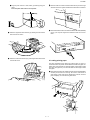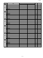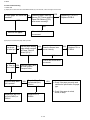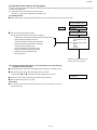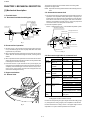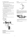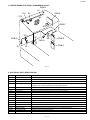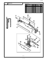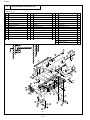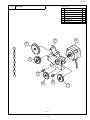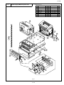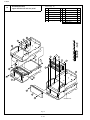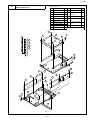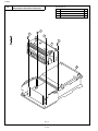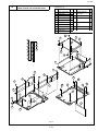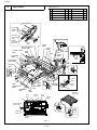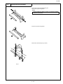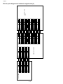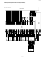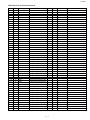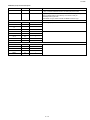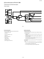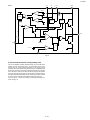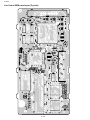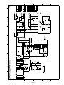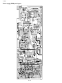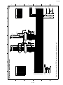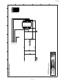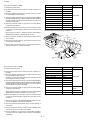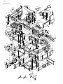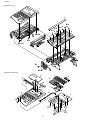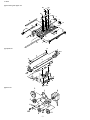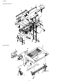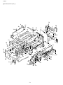
1
FO-6600U SERVICE MANUAL No. 00ZFO6600USME FACSIMILE MODEL FO-6600 CAUTION This laser printer is a class 1 laser product that complies with 21CFR 1040.10 and 1040.11 of the CDRH standard. This means that this machine does not produce a hazardous laser radiation. The use of controls, adjustments or performance of procedures other than those specified herein may result in hazardous radiation exposure. This laser radiation is not a danger to the skin, but when an exact focusing of the laser beam is achieved on the eyes retina, there is danger of spot damage to the retina. The following cautions must be observed to avoid exposure of the laser beam to your eyes at the time of servicing. 1) When a problem in the laser optical unit has occurred, the whole optical unit must be exchanged as a unit, not an individual part. 2) Do not look into the machine with the main switch turned on after removing the toner/developer unit and drum cartridge. 3) Do not look into the laser beam exposure slit of the laser optical unit with the connector connected when removing and installing the optical system. 4) The cover of Laser Printer Unit contains the safety interlock switch. Do not defeat the safety interlock by inserting wedges or other items into the switch slot. Laser Wave Length : 770-810 mm Laser Pulse Times : 49.2 µs Laser Output Power : 0.5 mW Parts marked with " " is important for maintaining the safety of the set. Be sure to replace these parts with specified ones for maintaining the safety and performance of the set. SHARP CORPORATION 1-1 This document has been published to be used for after sales service only. The contents are subject to change without notice. FO-6600U CONTENTS CHAPTER 1. GENERAL DESCRIPTION [1] Specifications . . . . . . . . . . . . . . . . . . . . . . . . . . . . . . . . . . . . . . . . . . . . . . . . . . . . . . . . . . . . . . . . . . 1-1 [2] Operation panel . . . . . . . . . . . . . . . . . . . . . . . . . . . . . . . . . . . . . . . . . . . . . . . . . . . . . . . . . . . . . . . . 1-2 [3] Transmittable documents . . . . . . . . . . . . . . . . . . . . . . . . . . . . . . . . . . . . . . . . . . . . . . . . . . . . . . . . . 1-4 [4] Installation . . . . . . . . . . . . . . . . . . . . . . . . . . . . . . . . . . . . . . . . . . . . . . . . . . . . . . . . . . . . . . . . . . . . 1-5 [5] Quick reference guide . . . . . . . . . . . . . . . . . . . . . . . . . . . . . . . . . . . . . . . . . . . . . . . . . . . . . . . . . . 1-10 CHAPTER 2. ADJUSTMENTS [1] Adjustments . . . . . . . . . . . . . . . . . . . . . . . . . . . . . . . . . . . . . . . . . . . . . . . . . . . . . . . . . . . . . . . . . . . 2-1 [2] Diagnostics and service soft switches . . . . . . . . . . . . . . . . . . . . . . . . . . . . . . . . . . . . . . . . . . . . . . . 2-2 [3] Troubleshooting . . . . . . . . . . . . . . . . . . . . . . . . . . . . . . . . . . . . . . . . . . . . . . . . . . . . . . . . . . . . . . . 2-37 [4] Error code table . . . . . . . . . . . . . . . . . . . . . . . . . . . . . . . . . . . . . . . . . . . . . . . . . . . . . . . . . . . . . . . 2-42 [5] Overseas communication mode . . . . . . . . . . . . . . . . . . . . . . . . . . . . . . . . . . . . . . . . . . . . . . . . . . . 2-43 CHAPTER 3. MECHANICAL DESCRIPTION [1] Mechanical description . . . . . . . . . . . . . . . . . . . . . . . . . . . . . . . . . . . . . . . . . . . . . . . . . . . . . . . . . . . 3-1 [2] Printer description . . . . . . . . . . . . . . . . . . . . . . . . . . . . . . . . . . . . . . . . . . . . . . . . . . . . . . . . . . . . . . 3-3 [3] Disassembly/assembly procedures . . . . . . . . . . . . . . . . . . . . . . . . . . . . . . . . . . . . . . . . . . . . . . . . 3-10 CHAPTER 4. DIAGRAMS [1] Block diagram . . . . . . . . . . . . . . . . . . . . . . . . . . . . . . . . . . . . . . . . . . . . . . . . . . . . . . . . . . . . . . . . . 4-1 [2] Wiring diagram . . . . . . . . . . . . . . . . . . . . . . . . . . . . . . . . . . . . . . . . . . . . . . . . . . . . . . . . . . . . . . . . . 4-2 [3] Point to point diagram and connector signal name . . . . . . . . . . . . . . . . . . . . . . . . . . . . . . . . . . . . . 4-3 CHAPTER 5. CIRCUIT DESCRIPTION [1] Circuit description . . . . . . . . . . . . . . . . . . . . . . . . . . . . . . . . . . . . . . . . . . . . . . . . . . . . . . . . . . . . . . . 5-1 [2] Circuit description of control PWB . . . . . . . . . . . . . . . . . . . . . . . . . . . . . . . . . . . . . . . . . . . . . . . . . . 5-1 [3] Circuit description of line control PWB . . . . . . . . . . . . . . . . . . . . . . . . . . . . . . . . . . . . . . . . . . . . . . 5-19 [4] Circuit description of TEL/LIU1 PWB . . . . . . . . . . . . . . . . . . . . . . . . . . . . . . . . . . . . . . . . . . . . . . . 5-22 [5] Circuit description of TEL/LIU2 PWB . . . . . . . . . . . . . . . . . . . . . . . . . . . . . . . . . . . . . . . . . . . . . . . 5-25 [6] Circuit description of CCD PWB . . . . . . . . . . . . . . . . . . . . . . . . . . . . . . . . . . . . . . . . . . . . . . . . . . . 5-28 [7] Circuit description of operation PWB . . . . . . . . . . . . . . . . . . . . . . . . . . . . . . . . . . . . . . . . . . . . . . . 5-28 [8] Circuit description of power supply PWB . . . . . . . . . . . . . . . . . . . . . . . . . . . . . . . . . . . . . . . . . . . . 5-29 [9] Circuit description of RS232C I/F PWB . . . . . . . . . . . . . . . . . . . . . . . . . . . . . . . . . . . . . . . . . . . . . 5-34 CHAPTER 6. CIRCUIT SCHEMATICS AND PARTS LAYOUT [1] Control PWB circuit . . . . . . . . . . . . . . . . . . . . . . . . . . . . . . . . . . . . . . . . . . . . . . . . . . . . . . . . . . . . . 6-1 [2] Line control PWB circuit . . . . . . . . . . . . . . . . . . . . . . . . . . . . . . . . . . . . . . . . . . . . . . . . . . . . . . . . . 6-20 [3] TEL/LIU 1, 2 PWB circuit . . . . . . . . . . . . . . . . . . . . . . . . . . . . . . . . . . . . . . . . . . . . . . . . . . . . . . . . 6-28 [4] Power supply PWB circuit . . . . . . . . . . . . . . . . . . . . . . . . . . . . . . . . . . . . . . . . . . . . . . . . . . . . . . . 6-33 [5] Operation panel PWB circuit . . . . . . . . . . . . . . . . . . . . . . . . . . . . . . . . . . . . . . . . . . . . . . . . . . . . . 6-35 [6] CCD PWB circuit . . . . . . . . . . . . . . . . . . . . . . . . . . . . . . . . . . . . . . . . . . . . . . . . . . . . . . . . . . . . . . 6-37 [7] RS232C I/F PWB circuit . . . . . . . . . . . . . . . . . . . . . . . . . . . . . . . . . . . . . . . . . . . . . . . . . . . . . . . . . 6-38 [8] Printer control PWB circuit . . . . . . . . . . . . . . . . . . . . . . . . . . . . . . . . . . . . . . . . . . . . . . . . . . . . . . . 6-40 CHAPTER 7. OPERATION FLOWCHART [1] Protocol . . . . . . . . . . . . . . . . . . . . . . . . . . . . . . . . . . . . . . . . . . . . . . . . . . . . . . . . . . . . . . . . . . . . . . 7-1 [2] Power on sequence . . . . . . . . . . . . . . . . . . . . . . . . . . . . . . . . . . . . . . . . . . . . . . . . . . . . . . . . . . . . . 7-2 CHAPTER 8. OTHERS [1] Service Tools . . . . . . . . . . . . . . . . . . . . . . . . . . . . . . . . . . . . . . . . . . . . . . . . . . . . . . . . . . . . . . . . . . 8-1 [2] IC signal name . . . . . . . . . . . . . . . . . . . . . . . . . . . . . . . . . . . . . . . . . . . . . . . . . . . . . . . . . . . . . . . . . 8-7 PARTS GUIDE 1–2 FO-6600U CHAPTER 1. GENERAL DESCRIPTION [1] Specifications Effective scanning width: 10.1" (256 mm) Applicable telephone line: Public switched telephone network Effective recording width: 8.0" (203 mm) Compatibility: ITU-T (CCITT) G3 mode Copy function: Configuration: Half-duplex, desktop transceiver Single/Multi-copy/Sort-copy (99 copies/page) Compression scheme: MH, MR, MMR and Sharp special mode Telephone function: Standard (cannot be used if power fails) Memory size*: 2 MB (approx. 108 average pages) Halftone (gray scale): 64 levels Memory option: 1 MB/2 MB/4 MB/16 MB Flash Memory Power requirements: 120 V AC, 60 Hz Scanning method: Flat-bed, solid-state CCD Operating environment: 50-86°F (10-30°C), 20 to 85% RH Resolution: Horizontal: Power consumption: Stand-by: 15 W • GENERAL 203 lines/inch (8 dots/mm) Maximum: 400 W Vertical: Dimensions: Standard-98 lines/inch (3.85 lines/mm) Width: 13.8" (351 mm) Depth: 22.9" (582 mm) Height: 18.5" (469 mm) Fine/Halftone-196 lines/inch (7.7 lines/mm) Weight: Approx. 59.8 lbs. (27.1 kg) Super fine-391 lines/inch (15.4 lines/mm) Printing density: Horizontal: • PRINTER SECTION 406 lines/inch (16 lines/mm) Vertical: Type: Desktop, Laser Beam Printer Print system: Electrostatic Dry Powdered Imaging System Exposure system: Laser Diode + Polygon Mirror Scanning Resolution: Horizontal: 406 (dot/inch) 391 lines/inch (15.4 lines/mm) Reception modes: Auto/Manual switching Modem speed: 33600 bps with automatic fallback to 31200, 28800, 26400, 24000, 21600, 19200, 16800, 14400, 12000, 9600, 7200, 4800, or 2400 bps Note: Transmission speeds in Super G3 mode may vary due to telephone line conditions. Transmission time*: Input document size: Vertical: 391 (dot/inch) Print speed: 6 pages per minute (Letter size paper) First print time: Within 19 seconds (face down) Approx. 3 seconds Warming-up time: Within 40 sec. Automatic feeding: Operating environment: Temperature: 10-30°C Humidity: 20-80%RH Width 5.8 to 11.0" (148 to 280 mm) Length 5.0 to 14.3" (128 to 364 mm) Manual feeding: Width 5.8 to 11.0" (148 to 280 mm) Toner cartridge life: 3,700 prints or more (when black-towhite ratio on print is 4% or less) Drum cartridge life: 20,000 prints or more (when blackto-white ratio on print is 5% or less) Length 5.0 to 17.0" (128 to 432 mm) Paper size: Width 8.5" (216 mm) * Length 11-14" (280-356 mm) Paper capacity: Based on ITU-T (CCITT) Test Chart #1 at standard resolution in Sharp special mode, excluding time for protocol signals (i.e., ITU-T phase C time only). 1150 sheets Automatic document feeder: 50 documents max. <IMPORTANT PLEASE READ FIRST> To avoid problems with supplies, please don’t use supplies from other units. Please use new supplies, when supply changes are required. 1–1 FO-6600U [2] Operation panel (1) LINE STATUS lights This LINE-1 lights illuminates when Line 1 is being used, and the LINE-2 lights illuminates when Line 2 is being used. LINE key Press this key before dialing to select the line. Display This displays messages and prompts during operation and programming. LINE-STATUS IN USE Service indicator This lights when a problem occurs which must be fixed by a service technician. Drum cartridge indicator This blinks when the drum cartridge nears the end of its life, and lights steadily when the drum cartridge needs replacement. LINE-2 LINE CHANGEOVER key Three types of information appear in the display: prompts related to operations you are performing, information about how the fax is using the line 1 (transmitting, receiving, etc.), information about how the fax is using the line 2. Press this key to switch through the three types of information. RESOLUTION key Press this key to adjust the resolution before sending or copying a document. RESOLUTION STANDARD FINE SUPER FINE HALF TONE CHANGEOVER Toner cartridge indicator This blinks when toner nears empty, and lights steadily when the toner/developer cartridge needs replacement. Paper out indicator This blinks when one of the paper sources (cassette) is out of paper, and lights steadily when all sources are out of paper. FUNCTION key SPEED DIAL key Press this key to dial Press this key to select a Speed Dial number. various special functions. BROADCAST key Press this key to send a document to a group of receiving fax machines. Telephone dial keypad (numeric keys) Use these keys to dial and program numbers. REPORT key Press this key to print out a report on the transaction just completed. COPY key Press this key to make a copy of a document. ABC 1 GHI MNO 5 COPY REPORT DOCUMENT SPEED DIAL BROADCAST COVER SHEET PRIORITY 6 TUV 7 FUNCTION 3 JKL 4 PRS DEF 2 DOCUMENT key Press this key to transmit a document without reading it into memory. WXY 8 REDIAL 9 OPER SPEAKER STOP START 0 REDIAL key Press this key to automatically redial the last number dialed. SPEAKER key Press this key to dial a number without picking up the handset. Note: This is not a speakerphone. You must pick up the handset to talk with the other party. STOP key Press this key to stop operations before they are completed. COVER SHEET key Press this key to include a cover sheet with a transmitted document. 1–2 START key Press this key to send or receive a document. PRIORITY key Press this key when you want to transmit a document ahead of other documents waiting in memory for transmission. FO-6600U Operation panel (2) RELAY key Press this key to send a document to another fax machine and have that machine in turn send the document to a number of end receiving machines. PAGE COUNTER key Press this key to have a slash and the total number of pages added after each page number on the pages of a transmitted document. Rapid Dial keys Press one of these keys to dial a fax or voice number automatically (these keys also serve as letter entry keys when storing a name). TIMER key Press this key to set an operation to be performed automatically at a later time. LIFE key Press this key, followed by the "1" key, to check the total number of pages printed by the fax machine. CONFIDENTIAL key Press this key to send or print out a confidential document. CONTRAST key Press this key to adjust the contrast before sending or copying a document. MEM. STATUS key Press this key to check the documents that have been scanned into memory for transmission. 01 02 03 04 05 06 07 08 33 34 35 36 37 38 39 A B C D E F G H A B C D E F G H 09 10 11 12 13 14 15 16 41 42 43 44 45 46 47 48 J K L M N O P I J K L M N O P I 17 18 19 20 21 22 23 24 CONTRAST PAGE COUNTER CONFIDENTIAL TIMER RELAY Q U Q R S T U V W X 25 26 27 28 29 30 31 32 Y Z SHIFT SP CLEAR CLEAR key Press this key to clear mistakes when storing names and numbers. SP key Press this key to enter symbols when storing a name. SHIFT key Press this key to switch between upper and lower case when storing a name. T V key, key Press these keys to move the cursor forward and backward when storing names and numbers. 1–3 MEM.STATUS SEARCH DIAL W DOWN X UP Z SPACE (Flip up the Rapid Key overlay) SPACE key Press this key to enter a space when storing a name. S DUPLEX SCAN Y SPACE R LIFE 40 SHIFT SP CLEAR DUPLEX SCAN key Press this key to transmit or copy two-sided documents. UP and DOWN keys Press these keys to adjust the volume of the handset when the handset is lifted, the volume of the speaker when the SPEAKER key has been pressed, or the volume of the ringer at all other times. SEARCH DIAL key Press this key to search by name for a number stored for automatic dialing. FO-6600U [3] Transmittable documents 4. Cautions on Transmitting Documents 1. Document Sizes Normal size width 5.83"–8.5"(148 – 216 mm) length 5.04" – 11"(128 – 279 mm) (Max.) 432mm (Max.) Letter size 279mm (Min.) 128mm 148mm • Documents written in yellow, greenish yellow, or light blue ink cannot be transmitted. • Ink, glue, and correcting fluid on documents must be dry before the documents can be transmitted. • All clips, staples and pins must be removed from documents be-fore transmission. • Patched (taped) documents should be copied first on a copier and then the copies used for transmission. • All documents should be fanned before insertion into the feeder to prevent possible double feeds. 5. Automatic Document Feeder Capacity 216mm [Normal size] Number of pages that can be placed into the feeder at anytime is as follows: 216mm [Special size] Normal size: max. 50 sheets (14 lbs – 20 lbs) Use document carrier sheet for smaller documents. Special size: single sheet only (manual feed) * With special sizes, only one sheet can be fed into the machine at a time. Insert next page into feeder as current page is being scanned. NOTES: 2. Paper Thickness & Weight Indication Weight Japanese indication indication Size 4 × 6 Metric system indication American indication LB system indication Thickness Metric system indication indication Inch system indication Document Document size size Range Number of Document size ADF sheets Weight Paper quality Kind • Product specifications Lower Limit Upper Limit 45kg paper 70kg paper When you need to send or copy more pages than the feeder limit, place additional pages in feeder when last page in feeder is being scanned. Place additional pages carefully and gently in feeder. If force is used, double-feeding or a document jam may result. 6. Readable Width & Length 52g/m2 80g/m2 The readable width and length of a document are slightly smaller than the actual document size. 14 LB 20 LB Note that characters or graphics outside the effective document scanning range will not be read. 0.06mm 0.1mm • Readable width 8.3" (208 mm) max. 0.0024" 0.0035" (148mm × 128mm) ~ W letter (279.4mm × 432mm) A4 (210mm × 297mm) Letter (216mm × 279mm) B6 ~ Letter/A4 size 50 sheets B4 size/Legal 20 sheets W letter size 1 sheet 90 kg (104g/m2) or more 135 kg (157g/m2) or less 1 sheet Paper of fine quality/bond paper/ Kent paper Readable width • 3. Document Types • • Readable length This is the length of the document sent minus 0.16" (4 mm) from the top and bottom edges. Normal paper Documents handwritten in pencil (No. 2 lead or softer), fountain pen, ball point pen, or felt-tipped pen can be transmitted. 4mm Documents of normal contrast duplicated by a copying machine can also be transmitted. • Readable length Diazo copy (blueprint) Diazo copy documents of a normal contrast may be transmitted. • Carbon copy 4mm A carbon copy may be transmitted if its contrast is normal. 1–4 FO-6600U 7. Use of Document Carrier Sheet A document carrier sheet must be used for the following documents. TELEPHONE JACK • • Those with tears. • Carbon-backed documents A standard RJ11C telephone jack must be located near the machine. This is the telephone jack commonly used in most homes and offices. • Plugging the fax machine into a jack which is not an RJ11C jack may result in damage to the machine or your telephone system. If you do not know what kind of jack you have, or need to have one installed, contact the telephone company. Those smaller than size 5.83" (W) × 5.04" (L) (148 mm (W) × 128 mm (L)). Make print straight across paper E.G. Place the document carrier in the document feeder with the clear film side down If the machine is moved from a cold to a warm place... If the machine is moved from a cold to a warm place, it is possible that the reading glass may fog up, preventing proper scanning of documents for transmission. To remove the fog, turn on the power and wait approximately 2 hours before using the machine. 2. Installing the printer cartridges (Toner cartridge: FO-45ND/Drum cartridge: FO-45DR) 1 Press the button on the side of the printer compartment, and open Direction of insertion NOTE: To transmit a carbon-backed document, insert a white sheet of paper between the carbon back of the document and the document carrier. • Those containing an easily separable writing substance (e.g., tracing paper written on with a soft, heavy lead pencil). NOTES: • • • • the printer cover. • Caution! The ribs on the bottom of the inside of the printer cover become very hot during printing. Be careful not to touch them. • If you are installing the cartridges for the first time, go to Step 4. When using the document carrier, carefully read the instructions written on the back. If the document carrier is dirty, clean it with a soft, moist cloth, and then dry it before using for transmission. Do not place more than one document in the carrier at a time. The thickness of document which can be held with the carrier sheet is up to 20 lb. 2 If you are replacing the cartridges, grasp the handle on the toner [4] Installation cartridge, and pull the toner cartridge out of the compartment. 1. Site selection Take the following points into consideration when selecting a site for this model. • If you are only replacing the drum cartridge, place the toner cartridge on a piece of paper on a horizontal surface. • If you are only replacing the toner cartridge, go to Step 6. ENVIRONMENT • • The machine must be installed on a level surface. • Provide easy access to the front, back, and sides of the machine. In particular, keep the area in front of the machine clear, or the original document may jam as it comes out after scanning. • • The temperature should be between 41° and 95°F (10° and 35°C). Keep the machine away from air conditioners, heaters, direct sunlight, and dust. The humidity should be between 30% and 85% (without condensation). ELECTRICITY A 120 V, 60 Hz, grounded (3-prong) AC outlet is required. 3 Pull the old drum cartridge out of the compartment. Caution! • Connection to a power source other than that specified will cause damage to the equipment and is not covered under the warranty. • If your area experiences a high incidence of lightning or power surges, we recommend that you install a surge protector for the power and telephone lines. Surge protectors can be purchased at most telephone specialty stores 1–5 FO-6600U 4 Remove the new drum cartridge from its packaging. 9 If you replace the toner cartridge, reset the toner counter by pressing the LIFE key (flip up the Rapid Key overlay if necessary), the "2" key, and the START key. LIFE 2 V F If you replace the drum cartridge, reset the drum counter by pressing 5 Align the arrowhead on the right side of the drum cartridge (the right the LIFE key (flip up the Rapid Key overlay if necessary), the "3" key, and the START key. side is marked "R") with the arrowhead pointing down on the right side of the compartment, and insert the cartridge into the compartment so that the ends of the cartridge move along the guides on the sides of the compartment. Make sure the cartridge is set firmly in place. • Place the old drum cartridge (if you removed one) in the empty drum cartridge bag, seal the bag, and dispose of it in a way that conforms to any local regulations that may exist in your area. • If you are not replacing the toner cartridge, go to Step 7. START LIFE V START 3 3. Assembly and connections 1 Connect the handset cord to the handset and the fax as shown. L • R1 The ends of the handset cord are identical, so they will go into either jack. Place the handset on the handset rest. Left Right 6 Remove the new toner cartridge from its packaging, and shake it several times as shown. • This ensures that the toner is well distributed inside the cartridge. Use the handset to make ordinary phone calls, or to transmit and receive documents manually. 7 Hold the handle of the toner cartridge so that the "2" marked on the 2 Connect the LINE 1 jack and the LINE 2 jack to the appropriate wall cartridge is to the right, and insert the cartridge into the com-partment that the two knobs on each side of the cartridge move along the two guides on each side of the compartment. Press the handle down so that the cartridge sets into place. • jacks with the telephone line cords. The wall jacks should be standard (RJ11C) single-line wall jacks for separate lines. Place the old toner cartridge (if you removed one) in the empty toner cartridge bag, seal the bag, and dispose of it in a way that conforms to any local regulations that may exist in your area. • Note: Voice communications, manual fax transmission and manual fax reception are only possible on Line 1. • The fax machine will only ring when a call is received on Line 1 (it will not ring when a call is received on Line 2). TEL. LINE 2 Left Right 8 Close the printer cover. LINE 1 LINE 2 1–6 TEL. LINE FO-6600U 3 Plug the power cord into a 120V, 60Hz, grounded (3-prong) AC 6 Insert the male end of the PC interface cable into the port on the right outlet. side of fax as shown. Tighten the attached screws with a screwdriver. Press the power switch to turn on the power. ON | OFF 0 7 Insert the female end of the PC interface cable into the serial (RS232C) 4 Attach the original document OUT tray by inserting the tabs into the port on your computer. Tighten the attached screws with a screwdriver. holes in the fax as shown. 5 Attach the received document tray by inserting the tabs into the holes in the fax as shown. 4. Loading printing paper The paper cassettes and the paper tray hold the paper on which received documents are printed. The FO-6600 comes with two paper cassettes. Each paper cassette can hold 500 sheets of either legal or letter size paper. The paper tray can hold 150 sheets of either legal or letter size paper. 1 Grasp the hand hold on the cassette as shown, lift the cassette slightly, and then pull it out as far as it will go. Do not force. Push down on green levers on both sides of the cassette tray as shown, and then pull it completely out of the fax using both hands. 1–7 FO-6600U 2 Pinch the ends of the paper guide together, and move the guide to 7 Rotate the received document tray back. Grasp the hand hold on the original document IN tray as shown, and open it. the appropriate position depending on whether you are loading letter or legal size paper. 8 Move the paper guide to the appropriate position depending on 3 Push the pressure plate down until it locks into position. whether you are loading letter or legal paper. • To remove the paper guide, press its inner side at the arrow marks and lift. 4 Place a stack of paper in the cassette, print side up. Make sure the two far corners of the paper go under the paper holders as shown. • LT Make sure the stack of paper is not higher than the tabs at the top of the paper guide. If it is, remove some of the paper. R LG L Letter Legal 9 Place the paper in the tray. 5 Put the cassette back in the fax. F Close the original document IN tray. 6 If desired, attach a letter or legal sticker as appropriate to the cassette. G If desired, attach a letter or legal sticker as appropriate to the fax as shown. 1–8 FO-6600U 5 Replace the drum cartridge, and then the toner cartridge. 5. Clearing paper jams If a document doesn’t feed through the scanner properly during transmission or copying, or DOCUMENT JAM appears in the display, first try pressing the START key. If the document doesn’t come out of the feeder, open the operation panel by squeezing the operation panel release on the right side of the operation panel (marked "PULL OPEN"), and gently pull out document. L R1 Left 1 Right 2 Left Right 6 Close the printer cover. 2 If the leading edge of the document is protruding from the printer compartment outlet, try pulling it out. • If you are unable to clear the paper jam in this way, continue with the following steps. 7 If you didn’t find any paper in the printer compartment, or if PAPER 3 Open the printer cover and remove the toner cartridge and drum cartridge. JAM still appears in the display after you close the printer cover, check each paper cassette and the paper tray. • • To release the cassette when pulling it out, press down on the levers on each side of the cassette. • To check the paper tray, grasp the hand hold on the original document IN tray and rotate the tray up. Caution! The ribs on the bottom of the inside of the printer cover become very hot during printing. Be careful not to touch them. 4 Gently pull the paper out of the compartment. • If the leading edge of the paper has entered the fusing unit, first pull the leading edge out of the fusing unit, then pull the paper out of the compartment. • Be sure to remove any torn pieced of paper. 8 Gently pull out any jammed paper you find, and then replace the cassette or close the original document IN tray. 1–9 FO-6600U [5] Quick reference guide FUNCTION key menu The following chart shows the layout of the functions and settings accessed by pressing the FUNCTION key. First press the FUNCTION key, the appropriate numeric key as shown, and then "#" or " " until the desired item appears. Instructions for making each setting appear in the display. Refer to the detailed instructions on the page shown below the setting. FUNCTION 1 Reception Mode 4 3 2 Entry Mode Optional Settings Activity Report Fax/Tel Numbers for Auto Dialing Fine Resolution Priority Timer List Telephone Number List Passcode Number Number of Rings in Auto Answer Mode Relay Group List Own Number and Name Set Number of Rings to Auto Manual Answer Date and Time Set Auto Listing Passcode List Option Setting List Program/Group List Batch Transmission List Department Usage List Confidential Reception List Day Light Saving ID Number System Number Store Junk Fax Number Department Code Mode 7 6 Listing Mode Print Hold Mode Program/Group Mode Retransmission Times Hold Data Print Program Entry Mode Retransmission Interval Print Hold Code Set Heater Mode Print Hold Code Clear Group Entry Mode Junk Fax Check Alarm Buzzer Transaction Report Print Select Dial Mode Recall Times Quick on Line Recall Wait Interval Multi TTI Security Selection Beep Length ECM Tel. Billing Code Auto cover Sheet Department Code Mode Memory Scanning Distinctive Ringing Anti Junk Fax Number List Copy Reduce Verification Stamp Copy Cut-off Print Hold Receive Reduce PC-Interface Mode Image Memory Print Receive Unit Cassette Selection Dial Selection Cassette Changeover Separate Mode Note: Steps which are optional are enclosed in a dotted frame: RESOLUTION LINE Transmitting documents Normal Dialing (1) Load document RESOLUTION Lift handset or press SPEAKER Dial (press numeric keys) START Wait for reception tone Normal Dialing (2) Lift handset or press SPEAKER Hang up Load document Dial (press numeric keys) RESOLUTION START Wait for reception tone Direct Keypad Dialing Hang up START Load document RESOLUTION LINE Dial (press numeric keys) Load document RESOLUTION LINE Press Rapid key Load document RESOLUTION LINE SPEED DIAL RESOLUTION REDIAL Rapid Key Dialing Speed Dialing Enter Speed Dial number (press numeric keys, -if less than 3 digits, press START to complete entry) START Redialing START Load document 1 – 10 Wait for reception tone 8 Serial Polling Mode 9 Memory Polling Mode Memory Polling Set Memory Polling Clear FO-6600U CHAPTER 2. ADJUSTMENTS (1) F102 (CCP2E20) is installed in order to protect IC’s from and overcurrent generated in the verification stamp drive circuit. If F102 is open, replace it with a new one. [1] Adjustments (2) F101, F103 (CCP2E30) is installed in order to protect IC’s from an overcurrent generated in the TX motor drive circuit. If F101, F103 is open, replace it with a new one. General Since the following adjustments and settings are provided for this model, make adjustments and/or setup as necessary. In addition to the replacement of F101, F103 and F102, the factor causing F101, F103 and F102 to open must also be repaired. If not, F101, F103 and F102 will open again. 1. Adjustments Replacement parts Adjustments of output voltage (FACTORY ONLY) CCP2E20 (Sharp code: VHVCCP2E20/-1) 1. Install the power supply unit in the machine. CCP2E30 (Sharp code: VHVCCP2E30/-1) 2. Set the recording paper and document. 3. Volume adjustment 3. When the document is loaded, power is supplied to the output lines. Confirm that outputs are within the limits below. You can adjust the volume of the speaker, handset, and ringer using the UP and DOWN keys on the operation panel (flip up the Rapid Key overlay to access the keys). Speaker The speaker has 3 volume levels: HIGH, MIDDLE, and LOW. To adjust the volume of the speaker, press the SPEAKER key and then press the UP or DOWN key until the desired level appears in the display. Press the SPEAKER key again to turn the speaker off. Handset The handset receiver has 3 volume levels: HIGH, MIDDLE, and LOW. To adjust the volume of the handset receiver, lift the handset and then press the UP or DOWN key until the desired level appears in the display. Ringer The ringer has 4 volume levels: HIGH, MIDDLE, LOW, and OFF. To adjust the volume of the ringer, press the UP or DOWN key until the desired level appears in the display (make sure the SPEAKER has not been pressed and the handset is not lifted). The fax will ring at the new volume level each time you change the level. If you select OFF, press the START key to confirm your selection. Output voltage settings POWER SUPPLY PWB CNPW CNPW CONTROL PWB Fig. 1 Output Voltage limits +5V +12V 4.75V~5.25V 11.5V~12.5V VM (+24V) 23.04V~24.96V Connector No. Pin No. 1 2 3 4 5 6 7 8 VM VM VM MG MG MG +5V +5V 4. Settings CNPW 9 DG 10 11 DG +12V 12 AG (1) Dial mode selector OPTION SETTING: DIAL MODE (Soft Switch No. SW2 DATA No. 1) Use this to set the fax machine to the type of telephone line you are on. • The factory setting is "TONE". OPTIONAL SETTING: DIAL MODE Soft Switch No. SW2 DATA No.1 for Line 1 No. SW15 DATA No.1 for Line 2 Use this to set the fax machine to the type of telephone line you are on. • The factory setting is "TONE". (step 1) Select "OPTION SETTING". KEY: FUNCTION 4 DISPLAY: 4:OPTION SETTING ENTER #01 33, (step 2) Select "DIAL MODE". KEY: 2. IC protectors replacement ICPs (IC Protectors) are installed to protect the TX motor drive circuit and verification stamp drive circuit. ICPs protect various ICs and electronic circuits from an overcurrent condition. 3 KEY: 1 DISPLAY: 1:LINE 1 KEY: CNPW F101 F102 1=TONE, 2=PULSE 2 CNPRT DISPLAY: 2:LINE 2 IC20 1=LINE 1,2=LINE 2 (step 3) Select "LINE", using "1" or "2". The location of ICPs are shown below: CONTROL PWB (TOP SIDE) 2 DISPLAY: 23:DIAL MODE 1=TONE, 2=PULSE F103 CNRS (step 4) Select, using "1" or "2". IC21 KEY: 1 DISPLAY: TONE SELECTED CNPN KEY: 2 DISPLAY: PULSE SELECTED (step 5) End, using the "STOP" key. Fig. 2 KEY: 2–1 STOP ,# FO-6600U [2] Diagnostics and service soft switch 1. Operating procedure 1-2. Print diagnosis Two kinds of diagnoses are supported. This diagnosis is concerned with the print which is used for production and service support. 1-1. Fax diagnosis Entering the diagnostic mode This diagnosis is concerned with the main body of fax which is used for production and service support. 9 Press FUNC display will appear. Entering the diagnostic mode 9 Press FUNC display will appear. MAIN: FBQ0 SUB: FBR0 8 Then press the START key. Select the desired item with key and the key or select with the rapid key. (Diag • specifications) key START key. (Diag • specifications) 9 the Enter the mode with the START key. Then press the START key. Select the desired item with the and the key or select with the rapid key. FUNC 6 , and the following PCU ROM Ver.: 7 , and the following FBQ1 FBR0 Enter the mode with the 8 FUNC 8 7 MAIN: FBQ0 SUB: FBR0 9 8 6 PCU ROM Ver.: FBQ1 FBR0 START START 01 START AREA PRINT MODE 02 START CHECK PATTERN 1 03 START CHECK PATTERN 2 04 START CHECK PATTERN 3 05 START PAPER FEED AGING 06 START BIAS ADJUST MODE 07 START LIFE SET MODE 08 START LIFE ALL CLEAR 09 START LIFE ENTRY MODE 01 START SOFT SWITCH MODE 02 START PRINT AREA 03 START ROM & RAM CHECK 04 START AUTO FEEDER MODE 05 START AGING MODE 06 START PANEL CHECK MODE 07 START OPTICAL ADJUST MODE 08 START PRODUCT CHECK 09 START SIGNAL SEND MODE 10 START TOP ADJUST MODE 10 START COMM. CHECK MODE 11 START LIFE CLEAR MODE 11 START MEMORY CLEAR 3) Memory clear when power is turned on 12 START FLASH MEMORY Pressing the START and STOP keys, turn on the main power, and the following message will be displayed. 13 START ALL FAX/TEL ENTRY MODE 14 START RS232C CHECK MODE 15 START DEPT. PASSCODE 16 START CONF. PASSCODE Here, when 1: YES is selected, the memory will be cleared to be ready for operation. 17 START PRINT HOLD CODE If 2: NO is selected, it will continue ready for operation as it is. 18 START MEMORY SET MODE 19 START MOTOR AGING 20 START STAMP AGING 21 START SCANNER SET MODE 22 START DIAL TEST MODE 23 START COPY DIAG MODE 24 START SIGNAL SEND MODE 2 MEMORY CLEAR EXECUTE ? 1 = YES , 2 = NO 2–2 FO-6600U 2. Diagnostic items description • 2-1. Fax diagnosis • 1) Soft switch mode In this mode, the soft switch are set and the soft switch list is printed. Soft switch mode screen Soft switch mode screen SOFT SWITCH MODE SW01=00000000 8 Switch 1 No. 1 Switch number selection • • • Data • Press START key for setting of the next soft switch. If the soft switch number is the final, pressing START key will exit the soft switch mode. Enter two digits of a soft switch number to set the switch number. If a switch number of unexisting soft switch is entered, key error buzzer sounds to reject the input. SOFT SWITCH MODE SW1 SOFT SWITCH MODE SW01=00000000 1 • SOFT SWITCH MODE SW16=00010110 6 2 Data number selection The cursor position shows the data to be set. Pressing # key moves the cursor to the right. If, however, the cursor is on data number 8, pressing # key shifts the cursor to data number 1 of the next switch number. If the switch number is the final, pressing # key will exit the soft switch mode. Pressing key moves the cursor to the left. If, however, the cursor is on data number 1, pressing key shifts the cursor to data number 1 of the former switch number. If the switch number is 1, pressing key will not move the cursor. • Mutual switch of ON/OFF of PC interface function during operation of image memory. When the PC interface board is not mounted, [Switch of OFF → ON of the item of "PC interface function" and of FAX → PC of the item of "automatic receiving in the PC interface mode] (Note: This supports not only the operation protect of the op-tional setting and soft switch mode but also an example of the automatic compensation of soft switch to OFF/FAX when the power is turned on even if the PC PWB is removed when the optional setting and soft switch mode are set at ON/PC.) (Though they are not provided, the existing model can operate without setting of the soft switch when it is not installed.) OFF to ON of multi TTI function and telephone billing code function when the department control function is OFF. OFF to ON of department control function during use of image memory. (Note: In the existing set, the department control function is set from OFF to ON when the timer communication (including the batch sending) or the memory hold is set.) ON to OFF of continuous serial polling function when the continuous serial polling is started. (Note: In the existing set, "ON to OFF of the continuous serial polling function when the continuous serial polling is registered" has been applied, but the conditions are now moderated. However, reg-istration is impossible to the program of the new continuous serial polling when the continuous serial polling function is OFF.) In addition, change of all soft switches during communication 7 Linked change of data (This is the same even in the optional setting.) • When the department control function is off, the multi TTI function and telephone billing code function are turned off. 2) Print area 3 Data setting method According to the size of the specified sheet, the effective printing area is printed. Press the FUNCTION key, and the data at the position of the cursor will be reversed to 0 when it is 1, or to 1 when it is 0. (If the soft switch can be changed at the bit (Refer to .), the error buzzer will sound with the process not received.) 3) ROM & RAM check 6 The sum value of ROM, the work and the back-up RAM are checked. The RS232C interface is also checked. If any error occurs, the buzzer will inform it. (Refer to the following table). Finally, the result will be printed. This diagnosis does not check the flash memory. The flash memory is checked with the flash memory test. 4 Outputting method of soft switch list In the soft switch mode, press the REPORT key, and the soft switch list will be output. If the recording paper runs out or is clogged, the key error buzzer will sound with the process not received. Number of buzzer sounds 5 Storage of data In the following case, the data of the soft switches set will be stored. • It is shifted to set the next soft switch by pressing the START switch. • It is shifted to set the next soft switch with the [#] key. • It is shifted to set the last soft switch with the [ ] key. • It is shifted to set another soft switch by inputting two digits as the switch number. (When 2 digits are completely input.) • Output of the soft switch list is started. 6 Inhibition of data change (This is also applicable for the optional setting.) In the following case, it is inhibited to change the data with the key error buzzer. • When the print hold bus code is not registered, the print hold func-tion is turned from OFF to ON. • When the print hold function is on, the print hold bus code is cleared. • When the memory is used because of substitutive receiving, etc, the print hold function is mutually turned on/off. • OFF to ON of telephone billing function which is using the image memory is used (Note: In the existing set, the telephone billing code function is specified from OFF to ON when the timer system com-munication (including the batch communication) is set.) Here, the memory is usable when the telephone billing code function is on. It can be set from ON to OFF while the memory is used. However, if setting is practically changed even once, it can not be returned from OFF to ON. Device checked Remarks 1 time <Short sound> ROM1 2 times <Short sounds> ROM2 Main Main 3 times <Short sounds> Integrated ROM/RAM Main 4 times <Short sounds> D-RAM Main 5 times <Short sounds> S-RAM Main *6 times <Short sounds> S-RAM (on the optional memory) Main 1 time <Long sound> ROM Sub 1 2 times <Long sounds> Integrated ROM/RAM Sub 1 3 times <Long sounds> D-RAM Sub 1 4 times <Long sounds> ROM Sub 2 5 times <Long sounds> Integrated ROM/RAM Sub 2 6 times <Long sounds> D-RAM Sub 2 * As practical, it is judged that the optional memory is not installed if any error occurs. Therefore, it does sometimes not sound. For the short and long sounds, one pattern is as follows. Main system: 0.25 seconds ON/0.25 seconds OFF Sub system: 1.00 second ON/0.25 seconds OFF The execution state of checking is as follows. Moreover, the list of the check result is output after checking is ended. Display during check Display after check ROM CPU SRAM DRM DPR ROM CPU SRAM DRM DPR ••••••• •• PPPPPPP E ••• •• P=PASS 2–3 PPP PP E=ERROR ROM/RAM check list output FO-6600U <Relationship between display and memory> When [PANEL CHECK MODE] is displayed, press the [START] key. The test will be started. When the test is started, LED’s will sequentially come on. It is used to check all LED’s. 2 Press any other key except [STOP] key. At this time, the name of each key will be displayed every push of the key. 3 However, if any key is pressed with the page plate opened, it will be equal to a press of key 32 with the page plate opened. 4 Finally press the [STOP] key. If all keys can be input, the key input "ALL KEY OK!!" will be displayed when the STOP key is ended. The screen will be all displayed in black, and the test result will be printed. In this test, it is okayed if all the other keys except [STOP] key have been pressed from start of the test to its end (the [STOP] key is pressed). If any key is skipped, it will be regarded as "KEY ERROR!!", and the name of the key not pressed will be printed on the list as the result. This will complete printing. • If the ten-key pad is used to input in this mode, DTMF corresponding to the pressed key is sent out continuously (lines 1/2 simultaneously). 1 Display during check ROM CPU SRAM DRM DPR ••••••• •• ••• •• Dual Port Ram for Comm. PWB Dual Port Ram for Comm. PWB DRAM(2Mbit) for Comm. PWB - SUB2 DRAM(2Mbit) for Comm. PWB - SUB1 DRAM(2Mbit) for Comm. PWB - MAIN SRAM(512kbit x 2) CPU - SUB2 CPU - SUB1 CPU - MAIN EPROM(16bit bus / 4Mbit) - SUB2 EPROM(16bit bus / 4Mbit) - SUB1 EPROM(8bit bus / 4Mbit x 2) - MAIN The check result of RS232C interface board is listed and printed together with the check result of ROM&RAM. 4) Auto feeder mode The auto feed function can be checked by inserting and discharging the document. (The distance between pages can be displayed during operation of the scanner.) 1 Check of auto feed function After this mode is activated, set up the document, and press the START key, and it will be automatically fed. (Before the START key is pressed, the document sensor alone is activated.) Moreover, the document size (A4/B4) and sensor information (A4/B4/ORG) are displayed when the document sensor is turned. 7) Optical adjust mode The document reading LED is turned on. 8) Product check The diagnosis is used in the production process. After shift to the mode, the following operations are sequentially executed. At this time, the sensor of read-error can be checked by feed-ing the B3 document. Set up one short document of B4 size. 04 : AUTO FEEDER MODE ( ) After setup of the document 1 Memory clear (Same as Diagnosis 11) 2 Panel test (Same as Diagnosis 06) 3 Dial test (Same as Diagnosis 24) 4 Document feed 5 Stamp press 6 ROM & RAM test, RS232C interface board check (Same as the Diagnosis 03) 7 Flash memory test mode (Same as Diagnosis 12) 8 Registration of fixed data 04 : AUTO FEEDER MODE B4 (A4 B4 ORG) Only the sensor which is activated (fallen down) is displayed.) The paper sheet size (A4/B4) is displayed. 2 Display of distance between pages during operation of the scanner • Soon after this mode is c\activated, press the FUNCTION key for 5 seconds or more, and the display mode of the distance between pages will be activated. Then, set up the sending paper and select the image quality, and then press the START key, and operation will be started. Be sure to press the FUNCTION key prior to the START key. If the FUNCTION key is not pressed but the START key is pressed, it will operate in the same manner as in the existing auto feeder mode. If the START key is pressed, the FUNCTION key will be invalid hereafter. Therefore, the display mode of the distance between pages and the existing mode can not be changed. • While the sending paper is read, the image quality key can be input. STD/FINE/S-FINE modes are usable. However, the same operation of FINE will be selected if the intermediate tone is set. • The image quality, the length of the sending page read, the page distance to the next sending paper and the total of the sending papers read are shown on the display. • When the stop key is pressed or 100 sending papers are read, the content shown on the display will be totally output as the list after the remaining sending papers are discharged. Registration of rapid key No. and other data necessary for production. The registered data are shown in the following table. The chain dial is not set for any destination. 5) Aging mode Rapid No. 01 FAX No. 20 Rapid No. 06 FAX No. 25 Rapid No. 11 FAX No. 1 Rapid No. 21 FAX No. 01 02 21 07 26 12 2 22 02 03 22 08 27 13 3 23 03 04 23 09 28 14 4 24 04 05 24 10 29 15 5 25 05 9 Transmission check (Same as Diagnosis 10) The soft switches necessary for production are set. F Test result print (two sheets) • AUTO FEEDER CHECK LIST • FLASH MEMORY CHECK LIST If any document is set up in the first state (when started), copying will be executed. If it is not set up, "check pattern 1" of the print diagnosis is output at the intervals of 1 time/60 minutes. (A total of 10 sheets are output.) Memory clear printing Panel test result printing ROM&RAM test result printing Check result printing of RS232C interface board 6) Panel check mode This is used to check whether each key is normally operated or not. According to the key input, LCD is displayed. Moreover, during exe-cution, the document reading lamp is turned on. G 2–4 Print area printing (one sheet) FO-6600U 9) Signal send mode 13) All FAX/TEL. entry mode After shift to the mode, press the START key, and the signals will be transmitted in the following sequence. It can be used to check the modem and so on. • The selection signal is sent out simultaneously from the lines 1/2 in this mode. The function is used to simplify the registration of FAX/TEL No. during aging. First, write the reference destination No. with the Rapid No. 01 key in the FAX No. registration mode before start of the diagnosis. 1 The diagnosis mode is activated. If anything is not registered in the Rapid No. 01 or any program or group is not registered, it will pass the diagnosis without doing anything. 2 The FAX/TEL No. (including the substitutive destination) of the Rapid No. 01 is copied to the Rapid Nos. 02 thru 48. 3 FAX No. of the Rapid No. 01 is copied to SPEED key Nos. 001 thru 200. 4 If any chain dial is not in the Rapid No., the Rapid Nos. 02 thru 48 and SPEED key Nos. 001 thru 200 are registered in the group No. 01. If any chain dial is not set, the group will be not produced but the chain dial setting alone of the Rapid No. 01 will be reset. (In all others except the Rapid No. 01, the chain dials will be continuously set as they are.) [ 1] No signals [ 2] 4800BPS (V27ter) [ 3] 14400BPS (V. 33) [ 4] 12000BPS (V. 33) [ 5] 14400BPS (V. 17) [ 6] 12000BPS (V. 17) [ 7] 9600BPS (V. 17) [ 8] 7200BPS (V. 17) [ 9] 9600BPS (V. 29) [10] 7200BPS (V. 29) (16th and subsequential letters of the destination name registered in the Rapid No. 01 will be discarded.) [11] 4800BPS (V27ter) [12] 2400BPS (V27ter) [13] 14) RS232C check mode 300BPS (FLAG) RS232C interface board is checked. When the interface board is installed, the result will be printed after the check. It is not installed, the following will be displayed. [14] 2100Hz (CED) [15] 1100Hz (CNG) 10) Comm. check mode 14: RS232C CHECK MODE I/F PWB NOT CONNECT 1 Turn on the line monitor. 2 Turn off the cover sheet function. The process will be ended after sounding of the error end buzzer. 3 Set 0 km at the line equivalence. 15) Dept. passcode 4 Bring the copy mode into the continuity mode. The department passcode list is printed. 16) Conf. passcode It is set to shift into the diagnosis mode when the SPEED key alone is pressed. After the check, it is necessary to be sure to return the aforemen-tioned soft switches into the initial state. (Clear the memory with the diagnosis.) 5 The confidential passcode list is printed. Differing from printing of one box alone soon after registration, the confidential passcodes of all boxes are printed. 17) Print hold code 11) Memory clear The print lockout passcode No. is printed. Clear the back-up memory to initialize the soft switches. The flash memory will be initialized. Then, the initialized list be output. 12) Flash memory The flash memory is checked. The ordinary memories (ROM, SRAM, DRAM) are checked in the ROM&RAM check process. The write/read test is taken every block to print the result. When an error occurs, the following error buzzer will sound. Number of buzzer sounds Check device 7 times <Short sounds> 8 times <Short sounds> Page memory Flash memory 9 times <Short sounds> Flash memory (optional) During operation of this diagnosis, dual operation is not possible at all. If this is excessively repeated, it will shorten the life of the flash memory. 2–5 FO-6600U 18) Memory set mode • Select the above items 1, 2 and 3 with the [ ] and [#] keys, and set the values with the [←] and [→] keys. The values can be set in the range of +3.0 mm to -3.0 mm at the 0.1 mm intervals. While the [←] and [→] key is continuously pressed one second or more, the setting value is automatically increased/decreased (in the range between the upper and lower limits). The set and dump list of the memory content is output. • The address (8 digits (P) generally including the bank information is input, and the data of 2 digits is continuously input. Inputting is done in the hexadecimal mode. The ten-key is used for 0 thru 9, and the alphabetic keys A (RAPID01 thru 06) are used for A thru F. • • During data inputting, the address can be moved forward and backward one byte by one byte with " " and "#". (The address prior to the address 0 is looped as the maximum address.) Input the quality selection key, and the value will be respectively set corresponding to the selected image quality. Here, the interme-diate tone is the same as for the setting value of FINE. • ±0.0 mm is default for all. • The Validity of the address is not checked. Accordingly, writ-ing/ reading operations are possible in the address of the memory not assigned, the address of ROM and so on. (However, as practical, writing is not done, and the data content runs short each reading.) Though writing is possible in the flash memory, a little time is required. It is also necessary to take care that the life of the flash memory is excessively shortened if much data is written in the flash memory. Since it may run away depending the written content, take minute care for the writing address. • <Drive conditions of motor> 4. Motor 5. Phase 6. Slow-up 7. Slow-down Specify the above values. • Setting values 4. 6 steps 5. Selection of one mode from 1-2 phase, 2-phase and micro step 6. 3 steps 7. 3 steps When the REPORT key is input, the memory dump list is produced from the displayed address (here, it is limited at the 16-byte boundary address (address with end 0) which does not exceed the specified address and is just in front.). The dump list is output to a maximum of 99 pages. If any data of one page can be repeatedly developed and printed, the list is sufficient. But it is not desired that the content of plural pages are developed in the memory once and are then printed. If the STOP key is pressed, it will pass to the diagnosis after the page which is now being printed is completed printed. If the address exceeds the maximum address, it will return to the address 0 and printing will be continued. • 19) Motor aging • Whether a document is present or not, the motor in the sending system is kept in rotation until the STOP key is pressed. • The image quality selection key can be input during stop alone to set the rotation speed for the image quality. (Here, the speed for FINE is selected when the intermediate tone is specified.) • The image quality for default at the start of execution is STD regardless of the image quality selection priority of the main body. • For rotation, the key "1" selects the 1-2 phase excitation, "2" selects the 2-phase excitation and "3" selects the micro step. It can not be changed during rotation. The 1-2 phase excitation is set as default. It is impossible if any document is not set up. • The document is fed at the 10 mm intervals, and is continuously stamped. • The total number of stamps from entry of the mode is displayed on the screen. • The ordinary operation aging which stamps a finish every docu-ment is executed in the ordinary copying mode. The mode is used to inspect whether dialing is accurate in two kinds of dial modes . All data which can be dialed in this mode are automatically called up in both PB mode and DP mode. When this mode is activated, the following operations will be automatically executed . Whether the dialed content is right or not is judged with the external instrument which is connected to the line cable. 1 After shift to the FAX diagnosis mode, press RAPID 24. (Also switch the display with the [ ] and [#] keys.) 2 Press the START key. 3 Turn on CML, and dial the following in the PB mode. 1, 2, 3, 4, 5, 6, 7, 8, 9, , 0, # 4 Turn off CML 500 mS alone. 5 Dial the following in the DP mode. 1, 5, 9, 0 6 After dialing, turn off CML. This mode uses the ordinary auto dial. (Accordingly, the signal send-ing time and minimum pause are all the same as ordinary. The measurement result in this mode is completely all the same as in the ordinary dial mode. Moreover, the same process as above is also done in the dial test mode which is executed in the product check mode. • The lines 1/2 operate simultaneously in this mode. 21) Scanner set mode • Input the quality selection key, and the value will be respectively set corresponding to the selected image quality. Here, the interme-diate tone is the same as for the setting value of FINE. 1. TOP 2. BOTTOM 3. LEFT 4. MOTOR 5. PHASE 6. SLOW UP 7. SLOW DOWN 22) Dial test mode 20) Stamp aging • Select the above items 4 thru 7 with the [ ] and [#] keys, and select the setting value with the ten-key. The reading width and motor drive conditions are set. <Reading width> 1. Top margin 2. Bottom margin 3. Left adjustment (The left position alone is specified.) Specify the above values. 2–6 FO-6600U 1. [Full black pattern] 2. [Intermediate tone 2 pattern] 23) Copy diag mode In order to shorten the process time during production, this mode is used to automatically switch the copy mode. Three menus are pro-vided. The left pattern is repeated. 1. 1 Set up two documents. (In case of two documents or more, there is no problem. 2 Press the START key. 3 Copy 1st document in the fine mode/density AUTO. (One sheet is printed in the ordinary copy mode.) 4 Copy 2nd (subsequential) document in the intermediate tone mode/density DARK. (In the ordinary copying mode, one sheet is printed when the RESOLUTION key is pressed three times.) 3. [Intermediate tone 1 pattern] The left pattern is repeated. When copy test is tried during production or is checked in two modes (fine and intermediate tones), this mode is provided to reduce the troublesome work which makes the operator stand aside to change the mode. Accordingly, the fine and intermediate tones are merely switched, and the mode is not switched to another mode. (Input of the image quality/ density key is invalid.) 2. Try the copy in the mode fixed at COPY REDUCE 95% and fine mode/density AUTO. At this time, don’t change the soft key of COPY REDUCE. (Input of the image quality/density key is invalid. 3. Continuously try the above items 1 and 2. 4. [Mesh point pattern] The left pattern is repeated. 24) Signal send mode 2 The signals concerned with V.34 & V.8 are checked. After this mode is activated, press the START key, and the signals will be sent in the following sequence. It can be used to check the modem. • The selection signal is sent out simultaneously from the lines 1/2 in this mode. [ 1] No signal [ 2] 33600BPS [ 3] 31200BPS 5. [Longitudinal strip 2 pattern] Black 2 dot and white 2 dot are repeated in line. [ 4] 28800BPS 6. [Lateral strip 2 pattern] Black 2 line and white 2 line are repeated. [ 5] 26400BPS 7. [Lateral strip 1 pattern] Black 1 line and white 1 line are repeated. [ 6] 24000BPS 8. [Full White pattern] [ 7] 21600BPS Rapid key 02: Check pattern 1 [ 8] 19200BPS The lateral stripe 2 pattern is printed on one sheet. (Black 2 line and white 2 line are repeated.) [ 9] 16800BPS Rapid key 03: Check pattern 2 [10] 14400BPS [11] 12000BPS The lateral stripe 2 pattern is printed on multiple pages. Press the STOP key to end the printing. [12] 9600BPS Rapid key 04: Check pattern 3 The intermediate tone 1 is printed on one sheet. [13] 7200BPS Rapid key 05: Paper feed aging [14] 4800BPS The mode is used for aging related to the printing. In this mode, the following modes are provided. 1 Blank paper aging mode (ALL WHITE AGING) 2 Whole black print aging mode (ALL BLACK AGING) 3 5% printing aging mode (5% AGING) 4 4% printing aging mode (4% AGING) After selecting the paper-pass aging mode in the print diagnosis mode, input the number of each mode above with the ten-key, and the mode will be executed. The detailed specifications of each mode are described as follows. Here, the operation in each mode is stopped only when the STOP key is pressed by the operator or a printing-impossible error occurs. [15] 2400BPS [16] V. 21 0-300bps [17] ANSam 2-2. Print diagnosis Rapid key 01: Area print mode The effective printing area frame is printed in the specified sheet size. 4mm ± 2.5 1. Full Black pattern 2. Intermediate tone 2 pattern 3. Intermediate tone 1 pattern 4. Mesh point pattern 5. Longitudinal strip 2 pattern 6. Lateral strip 2 pattern 7. Lateral strip 1 pattern 8. Full white pattern Pattern is repeated. 208mm 4mm ± 2 2–7 • Blank paper aging mode In the mode, printing is continued in the whole white (white paper) printing pattern until the STOP key is pressed by the operator. (In the printing area) • Whole black printing aging mode In the mode, printing is continued in the whole black (whole black) printing pattern until the STOP key is pressed by the operator. (In the printing area) FO-6600U Rapid key 6: Bias adjust mode set, the model which has the error display and RMS function will inform RMS when the counter reaches the set value. For setting, proceed with the following procedure. The mode is used to adjust the printing density of the printed image. The image printing density is adjustable in six steps of 1 to 6. For details, refer to the following table. (For selection, use the keys 1 thru 6.) Image printing density Thin ← 1 2 3 Default value 4 → Thick 5 6 1 When the life counter setting mode is selected, the following will be displayed. L I F E 1 = 0 0 0 0 0 0 O # key L I F E 2 = 0 0 0 0 0 0 key Rapid key 7: Life set mode The mode is used to set the life counter of the printer and the counter of the auto feeder at desired values. For setting, proceed with the following procedure. 1 L I F E 3 = 0 0 0 0 0 0 The cursor blinks at the top data. Three counters can be selected with the "#" and " " keys. When the life counter setting mode is selected, the following will be is displayed. M A C H I N E L I F E = 0 0 0 1 2 3 D R U M L I F E = 0 0 0 1 2 3 2 In the state 1 , input a desired setting number of 6 digits with the tenkey. 3 After input of 6 digits, shift to another counter with the "#" and " " keys as necessary. When all necessary counters are completely input, press the START key. 4 "STORED" will be displayed with the set values stored into the memory. For checking, retry this mode. L I F E 1 = 0 0 0 1 2 3 key # key L I F E 2 = 0 0 0 1 2 3 Note: L I F E 3 = 0 0 0 1 2 3 F E E D E R L I F E = 0 0 0 1 2 3 T O N E R L I F E = 0 0 0 1 2 3 The cursor blinks at the top data. Seven counters can be selected with the "#" and " " keys. 2 In the state 1, input a desired setting number of 6 digits with the tenkey. 3 After input of 6 digits, shift to another counter with the "#" and " " keys as necessary. When all necessary counters are completely input, press the START key. 4 "STORED" will be displayed with the set values stored into the memory. For checking, retry this mode. The counter shows the operational state of the printer (how many sheets have been printed since start of use? and oth-ers). The ordinary memory does not reset the counter. For clearing, set 0 in this mode or use the life counter clear mode in Item 3-9. (Accordingly, it is necessary to reset the counter or do the clear process in addition to the ordinary memory clear if the content in the memory on the control PWB is broken be-cause of PWB repair, etc. (In the production stage, it is neces-sary to execute this in the last process.) Rapid key 10: Top adjust mode As the method to adjust the top margin for printing, adjust top-margin adjusting VR on the PWB. If this mode is used at this time, adjust-ment is possible without the printing test every time when VR is turned. For the practical use, determine the adjusting value on the basis of the old data, and adjust to the determined value in this mode. Then, check it with the printing test. Rapid key 11: Life clear mode The mode is used to respectively clear the life counter of the printer and the counter of the auto feeder. For setting, proceed with the following procedure. Note: The counter shows the operational state of the printer (how many sheets have been printed since start of use? and others). The ordi-nary memory does not reset the counter. For clearing, set 0 in this mode or use the life counter clear mode in Item 3-9. (Accordingly, it is necessary to reset the counter or do the clear process in addition to the ordinary memory clear if the content in the memory on the control PWB is broken because of PWB repair, etc. (In the production stage, it is necessary to execute this in the last process.) 1 When the life counter clearing mode is selected, the following will be is displayed. Seven counters can be selected with the "#" and " " keys. M A C H I N E L I F E C L E A R D R U M L I F E C L E A R L I F E 1 C L E A R L I F E 2 C L E A R L I F E 3 C L E A R F E E D E R L I F E C L E A R T O N E R L I F E C L E A R Rapid key 08: Life all clear The mode is used to clear the life counter of the printer of the counter of the auto feeder. Note: # key The counter shows the operational state of the printer (e.g. how many sheets have been printed since start of use?). The ordinary memory does not reset the counter. For clearing, set 0 in the mode 8 or execute this mode. (Accordingly, it is nec-essary to reset this counter in addition to the ordinary memory clear if the content in the memory on the control PWB is broken because of PWB repair, etc. (In the production stage, it is necessary to execute this in the last process.) Rapid key 09: Life entry mode (For Serviceman temporary counter) The mode is used to set a desired value for the judgment value (alarm judgment counter value) of the general purpose life counters 1 thru 3 of the printer. If the life of a consumable part (developer,imprinter, etc) is 2–8 key 2 In the state 1, input the CLEAR key, and the counter will be respectively cleared. 3 After one clear, move the cursor to another counter with the "#" and " " keys as necessary, and then press the CLEAR key. When the necessary counters are completely cleared, press the STOP key. FO-6600U 3. How to make soft switch setting To enter the softswitch mode, make the following key entries in se-quence. Press FUNCTION 9 8 7 START 01 START SFT S W 1 = 0 0 0 0 0 0 0 0 Press FUNCTION key. SFT S W 1 = 1 0 0 0 0 0 0 0 Press key. Press key. SFT S W 1 = 1 0 0 0 0 0 0 0 SFT S W 1 = 1 0 0 0 0 0 0 0 Bit1 - 8 are set. SFT S W 1 = 1 0 0 0 0 0 0 0 Press START key during setting. SFT S W 2 = 0 0 0 0 0 0 0 0 Soft SW2 - 99 are set. S F T S W 99 = 0 0 0 0 0 0 0 0 To finish the settings halfway between SW 1 and SW99, press the STOP key. In this case, the setting being done to the SW No. on display will be nullified while settings done to the preceding SW Nos. remain in effect. The soft switch mode is terminated. • • SW1 to SW13: For line 1 SW14 to SW26: For line 2 2–9 FO-6600U 4. Soft switch description • Soft switch Note : SW1 to SW13 : For line 1, SW14 to SW26 : For line 2. SW DATA NO. NO. 1 2 Switch setting and function ITEM Recall interval 1 Binary input No. = 3 SW1 SW2 SW3 4 5 EX Recall attempts 8 1 4 2 2 3 1 4 (Data No.) 0 1 0 1 5 6 7 Initial setting Remarks 0 1 OPTION Set to 1~15 0 eg. Recall interval is set to 5 min. Binary input 8 4 2 1 1 0 6 No. = 7 8 EX 0 0 1 0 eg. Recall attempt times is set to 2 times. 8 (Data No.) OPTION 0 1 0 Set to 0~15 1 Dialing mode PULSE TONE 0 2 3 Receive mode ECM mode AUTO Off MANUAL On 1 0 4 Reserved 5 6 Polling security Auto cover sheet On No Off Yes 1 1 7 JUNK-FAX function in manual reception Yes No 0 8 1 JUNK-FAX function Number of rings for auto-receive Yes Binary input 0 0 OPTION OPTION 2 (0: No ring receive) 0 Set to 0~15 No. = 3 4 8 4 2 No 1 1 2 3 4 (Data No.) EX 0 0 0 1 eg. Number of rings for auto receive is set to 1. 5 Switch to auto-receive from manual receive 6 7 (0: No switch) OPTION 0 Binary input No. = EX 8 OPTION OPTION 0 1 8 4 2 1 0 OPTION 5 0 6 0 7 0 8 (Data No.) 0 0 0 Set to 0~15 eg. Switch to auto receive is set to disable. 0 Printed at Printed at Printed at Not printed Printed error only error/timer/ transmisevery time Communication results printout SW4 0 memory sion mode only only OPTION 1 No. 1 0 0 0 1 1 2 No. 2 0 0 1 0 1 0 0 3 4 No. 3 Image addition function to the communication On 1 0 0 Off 0 0 1 1 OPTION result table (for memory transmission only) SW5 5 6 Reserved TEL billing code function On Off 0 0 OPTION 7 Billing code position Before After 1 OPTION 8 1 Multi-TTI feature Time display format On 24 hours Off 12 hours-AM/PM 0 0 OPTION 2 Date display format Month-Day-Year Day-Month-Year 1 3 4 Header print Footer print Off On On Off 0 0 5 Relay data output No Yes 0 6 7 Substitute reception Substitute reception conditions Off On Reception disable without TSI Reception enable without TSI 0 0 8 CSI transmission Off 0 On 2 – 10 FO-6600U SW DATA NO. NO. Switch setting and function ITEM 1 1 MH fixed Yes 0 No (depend on remote machine) 2 H2 mode No Yes 3 4 Reserved Reserved SW6 0 0 V. 33 V. 17 V. 29 V. 27ter Default 14400 BPS MODEM 5 14400 12000 1440012000 9600 7200 9600 7200 4800 2400 No. 5 0 0 1 1 1 1 0 0 0 0 1 machine-1000 6 No. 6 1 1 0 0 0 0 0 0 0 0 0 (V. 17-14400) 7 8 No. 7 No. 8 0 0 1 0 0 0 1 0 0 1 1 1 0 1 1 1 1 0 0 0 0 0 Reception speed fixed NO 1 No. 1 0 2 No. 2 0 V. 17- V. 29- V. 27ter- 14400BPS 9600BPS 4800BPS 1 0 1 1 1 0 0 0 3 DIS receive acknowledge in G3 transmission Twice Once in NSF reception, twice in DIS reception 0 4 Non-modulated carrier in V.29 transmission mode On Off 0 5 EOL detection timer 25sec 13sec 0 6 7 Protocol monitor Line monitor On On Off Off 0 0 Max. length for TX/RX/Copy TX: 432mm, RX: unlimited SW7 When 14400BPS MODEM used, setting to 14400BPS is ignore. Effective to international comm. 8 Compromise Equalizer SW8 Remarks 0 0 Modem speed (DCS data reception speed) Initial setting TX/Copy: 432mm, RX: 1.5m constant (ROM) No Filter 1.8Km 0 variable (SRAM) 3.6Km 7.2Km 1 No. 1 0 0 1 1 0 2 3 No. 2 0 1 0 1 Reserved 1 0 4 Pause time 2 sec (1 sec from the second pause) 4 sec (2 sec from the second pause) 0 5 6 Signal transmission level Binary input No. = 1 0 8 5 4 6 2 7 1 8 (Data No.) 1 0 1 0 7 EX 8 Set to -(n+3)dBm eg. Signal transmission level is set to -11dBm 2 – 11 1 0 FO-6600U SW DATA NO. NO. 1 2 SW9 Switch setting and function ITEM CED tone signal interval CI signal OFF detect enable time 1 500ms 350ms or more 75ms 700ms or more 3 Equalizer freeze On Off 0 Equalizer freeze conditions Reserved All 7200bps 0 0 6 CED detection time 500ms 1000ms 7 8 Reserved Reserved 0 0 1 Reserved 0 2 3 Reserved Reserved 0 0 4 0 5 No. 5 OFF 0 6 No. 6 0 0 0 1 1 0 7 8 No. 7 No. 8 0 0 0 1 0 0 0 0 0 0 0 0 Memory retransmission times Binary input 2 3 No. = EX 4 5 6 RING2 0 RING3 1 0 8 4 2 1 1 1 1 2 0 3 1 4 (Data No.) 0 0 1 eg. Retransmission time set to 10 times. Memory retransmission interval Binary input No. = 8 5 4 6 2 7 1 8 (Data No.) 0 0 0 0 EX eg. Retransmission interval set to 5 min. 0 0 0 Reserved Reserved 0 3 No. 3 3sec 0 4 No. 4 0 1sec 0 1 No BEEP No BEEP 1 1 0 1 0 0 5 6 Action when RTN received Handle to no error V.34 mode function in case of manual communication On Handle to error Off 7 V.34 mode function On Off 8 1 V.34 control channel communication speed V.34 mode sending speed 2400bps 1200bps Sending speed = 2400 (bps) x N 0 1 Example: 1 2 3 4 2400 (bps) x 12 = 28800 (bps) 2400 (bps) is set for N = 0. SW13 0 1 1 1 0 33600 (bps) is set for N = 15. 5 6 V.34 mode receiving speed Receiving speed = 2400 (bps) x N Example: 1 1 7 2400 (bps) x 12 = 28800 (bps) 1 8 2400 (bps) is set for N = 0. 33600 (bps) is set for N = 15. 0 1 Reserved 0 2 3 Reserved Reserved 1 0 4 Reserved 1 5 6 Reserved Reserved 0 0 7 Reserved 1 8 Reserved 0 2 – 12 OPTION 0 0 0 8 1 Alarm buzzer SW14 STANDARD RING1 0 1 7 2 SW12 0 Reserved Distinctive ringing 1 Remarks 0 0 4 5 SW10 SW11 Initial setting 0 OPTION FO-6600U SW DATA NO. NO. SW15 SW16 SW17 SW18 Switch setting and function ITEM 1 Initial setting 0 1 2 Dialing mode Reserved PULSE TONE 3 Reserved 0 4 5 Reserved Reserved 0 1 6 Reserved 1 7 8 Reserved Reserved 0 0 1 Number of rings for auto-receive 2 3 (0 : No ring receive) Binary input No. = EX 4 0 1 8 4 2 1 0 OPTION 1 0 2 0 3 0 4 (Data No.) 1 0 0 Set to 0 ~15 eg. Number of rings for auto receive is set to 1. 1 5 6 Reserved Reserved 0 0 7 Reserved 0 8 1 Reserved Reserved 0 0 2 Reserved 0 3 4 Reserved Reserved 1 1 5 Reserved 0 6 7 Reserved Reserved 0 1 8 Reserved 0 1 2 Reserved Reserved 0 1 3 Reserved 0 4 5 Reserved Reserved 0 0 6 Reserved 0 7 8 Reserved Reserved 0 0 1 Reserved 0 2 3 Reserved Reserved 0 0 4 Reserved 0 SW19 Modem speed (DCS data reception speed) V. 33 V. 17 V. 29 V. 27ter 14400 12000 1440012000 9600 7200 9600 7200 4800 2400 Default 14400 BPS MODEM 5 No. 5 0 0 1 1 1 1 0 0 0 0 1 6 7 No. 6 No. 7 1 0 1 1 0 0 0 1 0 0 0 1 0 0 0 1 0 1 0 0 0 0 No. 8 0 0 0 0 1 1 1 1 0 0 0 8 Reception speed fixed NO 1 2 3 No. 1 0 No. 2 0 DIS receive acknowledge in G3 transmission Twice Remarks V. 17V. 29- V. 27ter14400PS 9600BPS 4800BPS 1 0 1 1 1 0 Once in NSF reception, twice 0 0 0 in DIS reception machine-1000 (V. 17-14400) When 14400BPS MODEM used, setting to 14400BPS is ignore. Effective to international SW20 comm. 4 Non-modulated carrier in V.29 On Off 0 transmission mode 5 6 EOL detection timer Protocol monitor 25sec On 13sec Off 0 0 7 Line monitor On Off 0 8 Reserved 0 2 – 13 FO-6600U SW DATA NO. NO. Switch setting and function ITEM 1 Compromise Equalizer constant (ROM) 1 2 SW21 No Filter 1.8Km 3.6Km 7.2Km 0 0 0 1 1 0 1 1 No. 1 No. 2 3 Reserved 4 5 Pause time Signal transmission level 0 variable (SRAM) Initial setting 0 1 0 2 sec (1 sec from the second pause) 4 sec (2 sec from the second pause) Binary input 8 4 2 1 6 No. = 7 8 EX 1 0 1 Set to -(n+3)dBm 5 6 7 0 1 8 (Data No.) 0 0 1 0 eg. Signal transmission level is set to -11dBm SW22 1 2 CED tone signal interval CI signal OFF detect enable time 3 Equalizer freeze On Off 0 4 5 Equalizer freeze conditions Reserved All 7200bps 0 0 6 CED detection time 500ms 1000ms 7 8 Reserved Reserved 0 0 1 Reserved 0 2 3 Reserved Reserved 0 0 4 SW23 SW24 SW25 500ms 350ms or more 75ms 700ms or more 0 0 0 Reserved 0 Distinctive ringing 5 No. 5 OFF 0 STANDARD 0 RING1 1 RING2 0 RING3 1 6 No. 6 0 0 0 1 1 0 0 7 8 No. 7 No. 8 0 0 0 1 0 0 0 0 0 0 0 0 1 Reserved 1 2 3 Reserved Reserved 0 1 4 Reserved 0 5 6 Reserved Reserved 0 0 7 Reserved 0 8 1 Reserved Reserved 0 0 2 Reserved 0 3 4 Reserved Reserved 0 0 5 Reserved 0 6 7 Reserved V.34 mode function On Off 1 1 8 V.34 control channel communication speed 2400bps 1200bps 0 1 2 V.34 mode sending speed Sending speed = 2400 (bps) x N Example: 1 1 3 2400 (bps) x 12 = 28800 (bps) 1 4 2400 (bps) is set for N = 0. 33600 (bps) is set for N = 15. 0 SW26 5 6 7 8 V.34 mode receiving speed Receiving speed = 2400 (bps) x N 1 Example: 2400 (bps) x 12 = 28800 (bps) 1 1 2400 (bps) is set for N = 0. 33600 (bps) is set for N = 15. 2 – 14 0 Remarks FO-6600U SW DATA NO. NO. Switch setting and function ITEM Line condition setting Line 1 RX 0 RX TX TX Line 2 TX/RX RX TX TX/RX TX TX/RX RX No. 1 No. 2 0 0 0 0 0 1 0 1 1 0 1 0 1 1 0 0 No. 3 0 1 0 1 0 1 0 0 1 2 3 SW27 4 Preference line specification Key buzzer volume LINE 2 Off 0 MIDDLE LOW No. 5 0 0 1 1 1 6 7 No. 6 0 1 0 1 Reserved 1 0 8 Reserved 1 No. 1 HIGH 0 HIGH 0 MIDDLE 1 LOW 1 1 2 No. 2 0 1 0 1 1 3 No. 3 HIGH 0 HIGH 0 MIDDLE 1 LOW 1 1 4 No. 4 0 1 0 1 0 5 No. 5 Off 0 HIGH 0 MIDDLE 1 LOW 1 1 6 No. 6 0 1 0 1 0 Handset volume Ringer volume SW29 LINE 1 HIGH 1 7 8 Reserved Reserved 0 0 1 Line to be used in PC I/F mode LINE 2 LINE 1 0 2 3 PC I/F mode Auto receive with PC I/F On PC Off FAX 0 0 4 Reserved 0 5 6 Reserved Reserved 0 0 7 Reserved 0 8 1 Reserved Reserved 0 0 2 Reserved 3 Continuous serial polling Dialing interval in continuous serial polling OPTION OPTION 0 On 0minute Off 30minutes 60minutes 120minutes 0 When SW30-3 SW30 is ON to be set 4 5 SW31 Remarks OPTION 5 Speaker volume SW28 Initial setting 1 TX/RX TX/RX TX/RX No. 4 No. 5 0 0 0 1 1 0 1 1 0 0 6 Reserved 7 8 Reserved Quick on-line 0 1 Reserved 0 2 3 Reserved Reserved 0 0 4 Reserved 0 5 6 Reserved Reserved 1 0 7 Reserved 1 8 Reserved 0 Yes No 2 – 15 0 1 by OPTION setting FO-6600U SW DATA NO. NO. Switch setting and function ITEM 1 Initial setting 0 1 Print hold On Off 0 2 Document transmission in Super G3 mode Yes No 0 3 Reserved 4 Changeover of print cassette On Selection of print cassette W cassette Auto. Remarks OPTION Refer to Page 2-44. 0 Off 1 TUL TLU UTL ULT LTU LUT OPTION Indicate of priority T...TRAY SW32 5 6 No. 5 No. 6 0 0 1 0 1 0 0 1 0 1 0 0 0 0 0 0 7 No. 7 0 0 0 0 0 1 1 0 8 No. 8 SEPA. 1 0 1 0 0 Selection of print cassette 0 1 0 Auto. U→L L→U MODE ON priority except in this table. No. 5 No. 6 0 0 0 1 0 0 0 0 7 No. 7 0 0 1 0 8 No. 8 0 1 0 0 Always on Always off Off timer 0 0 1 0 1 0 1 No. 1 2 Density adjustment of print bias SW33 Indicate of Work in auto mode 5 6 Heater mode No. 2 Binary input 4 2 0 1 3 4 5 No. = 4 5 EX 0 1 1 eg. Bias is set to level 3. Drum life limit U...UPPER L...LOWER 0 OPTION set to 1~6. 3 6 U...UPPER L...LOWER (Data No.) 1: faint 6: deep 0 near = 19,000 pcs. 0 near = 15,000 pcs. 0 set to 0,7 is 1 1 equal to 3 (001). 0 1 near = 15,000 pcs. 1 near = 16,000 pcs. 7 0 limit = 20,000 pcs. 1 limit = 16,000 pcs. 0 limit = 20,000 pcs. 1 limit = 20,000 pcs. 8 Reserved 1 2 Start time of heater OFF timer (Upper digit of hour) 3 SW34 Start time of heater OFF timer 6 (Lower digit of hour) 7 8 SW35 Binary input No. = 8 1 4 2 2 3 1 4 (Data No.) 0 0 0 0 Start time of heater OFF timer 2 3 (Upper digit of minute) Binary input 0 8 4 2 1 5 6 7 8 (Data No.) 0 OPTION OPTION 0 0 8 4 2 1 0 No. = EX 1 0 2 0 3 0 4 (Data No.) 0 0 0 Binary input No. = 8 5 4 6 2 7 1 8 (Data No.) 0 0 0 0 4 OPTION 0 Start time of heater OFF timer (Lower digit of minute) 7 EX 8 1 End time of heater OFF timer 2 (Upper digit of hour) 3 4 5 End time of heater OFF timer 6 7 (Lower digit of hour) 8 0 0 0 0 EX 0 0 0 0 eg. Start time is set to 15: XX 1 5 6 SW36 0 Binary input No. = EX 4 5 0 eg. Start time is set to XX: 40 Binary input 8 4 2 1 0 0 0 0 0 No. = 1 2 3 4 (Data No.) 0 EX 0 0 0 0 0 0 8 4 2 1 0 5 0 6 0 7 0 8 (Data No.) 0 0 0 Binary input No. = EX eg. End time is set to 21: XX 2 – 16 OPTION 0 OPTION OPTION FO-6600U SW DATA NO. NO. 1 2 End time of heater OFF timer (Upper digit of minute) 3 SW37 SW39 SW40 SW41 1 Binary input No. = EX 4 5 End time of heater OFF timer 6 (Lower digit of minute) 7 8 SW38 Switch setting and function ITEM Binary input No. = 0 Initial setting 8 1 4 2 2 3 1 4 (Data No.) 0 0 0 0 0 0 0 8 4 2 1 0 0 5 6 7 8 (Data No.) 0 EX 0 0 0 0 eg. End time is set to XX: 35 0 0 1 Reserved 1 2 3 Reserved Reserved 0 0 4 Reserved 0 5 6 Reserved Reserved 0 0 7 Reserved 0 8 1 Reserved Reserved 0 0 2 Reserved 1 3 4 Reserved Reserved 0 0 5 Reserved 0 6 7 Reserved Reserved 0 0 8 Reserved 0 1 2 Reserved Reserved 1 0 3 Reserved 0 4 5 Reserved Reserved 0 0 6 Reserved 0 7 8 Reserved Reserved 0 0 1 Reserved 0 2 3 Reserved Reserved 0 1 4 Reserved 0 5 6 Reserved Reserved 0 1 7 Reserved 0 8 Reserved 1 2 – 17 Remarks OPTION OPTION FO-6600U SW DATA NO. NO. SW42 SW43 Switch setting and function ITEM 1 Initial setting 0 1 2 Reserved Reserved 0 0 3 Reserved 1 4 5 Reserved Reserved 0 0 6 Reserved 1 7 8 Reserved Reserved 0 1 1 Reserved 1 2 3 Reserved Reserved 0 0 4 Reserved 0 5 6 Reserved Reserved 0 1 7 Reserved 0 8 1 Reserved Automatic printing of activity report Yes (When memory full) 1 0 No (First data is cleared Remarks OPTION when memory full) SW44 2 Printout of total time and total number of pages on activity report 3 Reserved 4 5 Department function Department ID digit Off On 0 On Binary input 0 0 OPTION Set is 3~9. 0 8 4 2 Off 1 5 6 7 6 No. = 8 (Data No.) 1 7 8 EX 0 1 0 0 eg. Department ID is set to 4 digits. 0 0 1 Picture quality priority mode Fine Standard 0 OPTION 2 3 Cut-off mode (when copy mode) Scanning ratio in memory input Continue 1:1 Cut-off Reduce 0 0 OPTION Memory 4 Verification STAMP Yes No 0 5 Overseas communication mode selection Yes No 0 scanning SW45 function Reduce ratio (when copy mode) Invalid if not mounted. Refer to Page 2-44. AUTO 100% 95% 89% 74% 6 No. 6 0 1 0 0 1 1 7 8 No. 7 No. 8 0 0 0 0 1 0 0 1 1 0 0 0 2 – 18 FO-6600U SW DATA NO. NO. Switch setting and function ITEM 1 Reserved 2 Reserved 1 Initial setting 0 0 0 Density adjustment (when Fine/STD mode) Normal Faint Deep 0 0 0 1 1 0 Normal Faint Deep Deep (when Dark mode) SW46 3 4 No. 1 No. 2 Density adjustment (when Half-tone mode) 1 1 0 0 Deep (when Dark mode) SW47 SW48 SW49 SW50 SW51 5 No. 3 0 0 1 1 0 6 7 No. 4 0 1 0 1 HTF correction in Half-tone mode On Off 0 1 8 MTF correction in Half-tone mode Strong Weak 1 2 Reserved Reserved 0 0 3 Reserved 0 4 5 Reserved Reserved 0 0 6 Reserved 0 7 8 Reserved Reserved 0 0 1 Reserved 0 2 3 Reserved Reserved 0 0 4 Reserved 0 5 6 Reserved Reserved 0 0 7 Reserved 0 8 1 Reserved Reserved 0 0 2 Reserved 0 3 4 Reserved Reserved 0 0 5 Reserved 0 6 7 Reserved Reserved 0 0 8 Reserved 0 1 2 Reserved Reserved 0 0 3 Reserved 0 4 5 Reserved Reserved 0 0 6 Reserved 0 7 8 Reserved Reserved 0 0 1 Reserved 0 2 3 Reserved Reserved 0 0 4 Reserved 0 5 6 Reserved Reserved 0 0 7 Reserved 0 8 Reserved 0 2 – 19 0 Remarks FO-6600U SW DATA NO. NO. SW52 SW53 SW54 SW55 SW56 Switch setting and function ITEM 1 1 Reserved 0 2 3 Reserved Reserved 0 0 4 Reserved 0 5 6 Reserved Reserved 0 0 7 Reserved 0 8 1 Reserved Reserved 0 0 2 Reserved 0 3 4 Reserved Reserved 0 0 5 Reserved 0 6 7 Reserved Reserved 0 0 8 Reserved 0 1 2 Reserved Reserved 0 0 3 Reserved 0 4 5 Reserved Reserved 0 0 6 Reserved 0 7 8 Reserved Reserved 0 0 1 Reserved 0 2 3 Reserved Reserved 0 0 4 Reserved 0 5 6 Reserved Reserved 0 0 7 Reserved 0 8 1 Reserved Reserved 0 1 2 Reserved 1 3 4 Reserved Reserved 1 1 5 Printing when toner empty Printing Reduction of print data SW57 Initial setting 0 Stop 0 6 No. 6 AUTO 0 7 No. 7 0 0 1 0 1 0 8 1 No. 8 0 0 0 1 0 Reserved 0 0 2 Reserved 0 3 4 Reserved Reserved 0 0 5 Reserved 0 6 7 Reserved Reserved 0 0 8 Reserved 0 2 – 20 100% 1 Remarks 94%(92%) 88%(86%) 73%(72%) 0 0 1 0 The number in () is applicable for the footer print on. AUTO is equivalent to 100 %. FO-6600U SW DATA NO. NO. SW58 SW59 SW60 SW61 SW62 SW63 ITEM Switch setting and function 1 0 Initial setting 1 Reserved 0 2 Reserved 0 3 4 Reserved Reserved 0 0 5 Reserved 0 6 7 Reserved Reserved 0 0 8 Reserved 0 1 2 Reserved Reserved 0 0 3 Reserved 0 4 5 Reserved Reserved 0 0 6 Reserved 0 7 8 Reserved Reserved 0 0 1 Reserved 0 2 3 Reserved Reserved 0 0 4 Reserved 0 5 6 Reserved Reserved 0 0 7 Reserved 0 8 1 Reserved Reserved 0 0 2 Reserved 0 3 4 Reserved Reserved 0 0 5 Reserved 0 6 7 Reserved Reserved 0 0 8 Reserved 0 1 2 Reserved Reserved 0 0 3 Reserved 0 4 5 Reserved Reserved 0 0 6 Reserved 0 7 8 Reserved Reserved 0 0 1 Reserved 0 2 3 Reserved Reserved 0 0 4 Reserved 0 5 6 Reserved Reserved 0 0 7 Reserved 0 8 Reserved 0 2 – 21 Remarks FO-6600U SW DATA NO. NO. SW64 SW65 SW66 SW67 SW68 Switch setting and function ITEM 1 0 Initial setting 1 Reserved 0 2 3 Reserved Reserved 0 0 4 Reserved 0 5 6 Reserved Reserved 0 0 7 Reserved 0 8 1 Reserved Reserved 0 0 2 Reserved 0 3 4 Reserved Reserved 0 0 5 Reserved 0 6 7 Reserved Reserved 0 0 8 Reserved 0 1 2 Reserved Reserved 0 0 3 Reserved 0 4 5 Reserved Reserved 0 0 6 Reserved 0 7 8 Reserved Reserved 0 0 1 Reserved 0 2 3 Reserved Reserved 0 0 4 Reserved 0 5 6 Reserved Reserved 0 0 7 Reserved 0 8 1 Reserved Reserved 0 0 2 Reserved 0 3 4 Reserved Reserved 0 0 5 Reserved 0 6 7 Reserved Reserved 0 0 8 Reserved 1 2 Cassette define (LTR/A4): Tray Cassette define (LTR/A4): Upper Remarks 0 A4 A4 LTR LTR 0 0 When W cassette 3 Cassette define (LTR/A4): Lower A4 LTR 0 4 Separation of image area in the half-tone On Off 1 5 6 Removal of notch in the binary mode Reserved On Off 1 1 7 Reserved 1 8 Reserved 0 SW69 2 – 22 Ignore when W cassette. FO-6600U SW DATA NO. NO. SW70 Switch setting and function ITEM 1 Initial setting 0 1 Reserved 1 2 Reserved 1 3 4 Reserved Reserved 1 1 5 Reserved 0 6 7 Reserved Reserved 0 0 8 Reserved Black line detection (When transmission scanning) 0 Continued black line count when detected 1 2 3 4 5 6 7 Unused 1 No. 1 0 0 0 0 0 0 0 0 0 2 3 No. 2 No. 3 0 0 0 0 0 1 0 1 1 0 1 0 1 1 1 1 0 1 No. 4 0 1 0 1 0 1 0 1 1 4 All white page detection (When transmission scanning) All white line count ratio against total count of page to judge the white page Unused 1.0% 1.5% 2.0% 2.5% 3.0% 3.5% 4.0% SW71 5 6 No. 5 No. 6 0 0 0 0 0 0 0 0 0 1 0 1 0 1 0 1 0 1 7 No. 7 0 0 1 1 0 0 1 1 0 No. 8 0 1 0 1 0 1 0 All white line count ratio against total count of page to 1 1 8 judge the white page No. 5 6 No. 6 0 0 0 0 1 1 1 1 7 8 No. 7 No. 8 0 0 0 1 1 0 1 1 0 0 0 1 1 0 1 1 Black line detection Continued black line count when detected (When copy scanning) SW72 4.5% 5.0% 5.5% 6.0% 7.0% 8.0% 9.0% 10.0% 1 1 1 1 1 1 1 1 5 1 No. 1 1 0 2 0 3 0 4 0 5 0 6 0 7 0 Unused 0 0 2 No. 2 0 0 0 0 1 1 1 1 0 3 4 No. 3 No. 4 0 0 0 1 1 0 1 1 0 0 0 1 1 0 1 1 1 1 White page detect All white line count ratio against total count of page to (When copy scanning) judge the white page Unused 1.0% 1.5% 2.0% 2.5% 3.0% 3.5% 4.0% 5 No. 5 0 0 0 0 0 0 0 0 0 6 7 No. 6 No. 7 0 0 0 0 0 1 0 1 1 0 1 0 1 1 1 1 1 0 No. 8 0 1 0 1 0 1 0 1 1 8 All white line count ratio against total count of page to judge the white page 4.5% 5.0% 5.5% 6.0% 7.0% 8.0% 9.0% 10.0% SW73 5 6 No. 5 No. 6 1 0 1 0 1 0 1 0 1 1 1 1 1 1 1 1 7 No. 7 0 0 1 1 0 0 1 1 8 1 No. 8 0 1 0 1 0 1 0 1 Reserved 1 2 Reserved 0 3 4 Reserved Reserved 0 0 5 Reserved 0 6 7 Reserved Reserved 0 0 8 Reserved 1 2 – 23 Remarks FO-6600U SW DATA NO. NO. SW74 SW75 SW76 SW77 Switch setting and function ITEM 1 0 Initial setting 1 2 Reserved Reserved 0 1 3 Reserved 1 4 5 Reserved Reserved 0 0 6 Reserved 0 7 8 Reserved Reserved 0 0 1 Reserved 0 2 3 Reserved Reserved 1 0 4 Reserved 0 5 6 Reserved Reserved 0 0 7 Reserved 0 8 1 Reserved Reserved 0 1 2 Reserved 1 3 4 Reserved Reserved 1 1 5 Reserved 1 6 7 Reserved Reserved 1 0 8 Reserved 0 1 2 Reserved Reserved 0 0 3 Reserved 0 4 5 Reserved Reserved 0 0 6 Reserved 0 7 8 Reserved Reserved 0 0 1 Secure billing code Yes No 0 2 Pause with Z key Yes No 0 Remarks Only when special billing code is given. SW78 3 4 Reserved Z key pause time 5 250 ms unit Binary input No. = 16 8 4 2 1 0 0 4 6 7 8 (Data No.) 0 5 6 7 EX 0 0 0 0 0 eg. Pause time 250 ms 0 0 8 Time = (n + 1) x 250 ms 0 Only when the special billing code is given The ordinary pause is not affected. SW79 1 Reserved 1 2 Reserved 1 3 4 Reserved Reserved 1 1 5 Reserved 0 6 7 Reserved Reserved 0 0 8 Reserved 0 2 – 24 FO-6600U SW DATA NO. NO. SW80 SW81 SW82 SW83 SW84 SW85 ITEM Switch setting and function 1 0 Initial setting 1 2 Reserved Reserved 0 0 3 Reserved 1 4 5 Reserved Reserved 1 0 6 Reserved 1 7 8 Reserved Reserved 1 0 1 Reserved 0 2 3 Reserved Reserved 0 0 4 Reserved 0 5 6 Reserved Reserved 1 0 7 Reserved 0 8 1 Reserved Reserved 0 1 2 Reserved 0 3 4 Reserved Reserved 0 1 5 Reserved 0 6 7 Reserved Reserved 0 1 8 Reserved 1 1 2 Reserved Reserved 0 1 3 Reserved 0 4 5 Reserved Reserved 0 0 6 Reserved 1 7 8 Reserved Reserved 1 0 1 Reserved 0 2 3 Reserved Reserved 0 1 4 Reserved 0 5 6 Reserved Reserved 0 0 7 Reserved 0 8 1 Reserved Reserved 1 0 2 Reserved 0 3 4 Reserved Reserved 1 0 5 Reserved 0 6 7 Reserved Reserved 0 0 8 Reserved 1 2 – 25 Remarks FO-6600U SW DATA NO. NO. SW86 Switch setting and function ITEM 1 1 F.A.S.T. (RMS) mode On Off 0 2 3 F.A.S.T. (RMS) line Day light saving time feature LINE 2 On LINE 1 Off 0 0 4 Separate mode On Off 5 6 Reserved Reserved 7 CNG send when manual TX On Off 1 8 1 Ringer of line 2 Reserved On Off 0 0 2 No. 2 3 No. 3 SW87 SW89 SW90 SW91 0 0 0 Addition of header to various lists SW88 Initial setting 0 Relay instruction transmission line specification Without Information Information Without addition of line 1 0 0 addition 1 0 0 of line 2 1 0 1 0 1 AUTO Line 1 Line 2 Not used (AUTO) 4 No. 4 0 0 1 1 0 5 6 No. 5 0 1 0 1 Reserved 1 1 7 Reserved 0 8 1 Reserved Reserved 0 0 2 Reserved 1 3 4 Reserved Reserved 0 0 5 Reserved 0 6 7 Reserved Reserved 0 0 8 Reserved 0 1 2 Reserved Reserved 0 0 3 Reserved 0 4 5 Reserved Reserved 0 0 6 Reserved 0 7 8 Reserved Reserved 0 0 1 Reserved 0 2 3 Reserved Reserved 0 0 4 Reserved 0 5 6 Reserved Reserved 0 0 7 Reserved 0 8 1 Reserved Reserved 0 0 2 Reserved 0 3 4 Reserved Reserved 0 0 5 Reserved 0 6 7 Reserved Reserved 0 0 8 Reserved 0 2 – 26 Remarks OPTION FO-6600U SW DATA NO. NO. SW92 SW93 SW94 SW95 SW96 SW97 ITEM Switch setting and function 1 0 Initial setting 1 Reserved 0 2 3 Reserved Reserved 0 0 4 Reserved 0 5 6 Reserved Reserved 0 0 7 Reserved 0 8 1 Reserved Reserved 0 0 2 Reserved 0 3 4 Reserved Reserved 0 0 5 Reserved 0 6 7 Reserved Reserved 0 0 8 Reserved 0 1 2 Reserved Reserved 0 0 3 Reserved 0 4 5 Reserved Reserved 0 0 6 Reserved 0 7 8 Reserved Reserved 0 0 1 Reserved 0 2 3 Reserved Reserved 0 0 4 5 Reserved Reserved 0 0 6 Reserved 0 7 8 Reserved Reserved 0 0 1 Reserved 0 2 3 Reserved Reserved 0 0 4 Reserved 0 5 6 Reserved Reserved 0 0 7 Reserved 0 8 1 Reserved Reserved 0 0 2 Reserved 0 3 4 Reserved Reserved 0 0 5 Reserved 1 6 7 Reserved Reserved 1 1 8 Reserved 1 2 – 27 Remarks FO-6600U SW DATA NO. NO. SW98 SW99 ITEM Switch setting and function 1 0 Initial setting 1 Reserved 0 2 3 Reserved Reserved 0 0 4 Reserved 0 5 6 Reserved Reserved 0 0 7 Reserved 0 8 1 Reserved Reserved 0 0 2 Reserved 0 3 4 Reserved Reserved 0 0 5 Reserved 0 6 7 Reserved Reserved 0 0 8 Reserved 0 2 – 28 Remarks FO-6600U • • • Soft switch function description SW1 No. 1 ~ No. 4 Recall interval SW1 to SW13: For line 1 SW14 to SW26: For line 2 Choice is made for a recall interval for speed and rapid dial-numbers. Use a binary number to program this. If set to 0 accidentally, 1 will be assumed. SW1 No. 5 ~ No. 8 Recall attempts Choice is made as to how many recall attempts should be made. Use a binary number to program this. SW2 No. 1 Dialing mode Switch the type according to the telephone circuit connected to the facsimile. 0: PULSE DIAL 1: TONE DIAL SW2 No. 2 Receive mode Auto/manual receiving mode is set. SW2 No. 3 ECM mode Used to determine ECM mode function. Refer to the following table. SW2-No.3 ECM MODE 0 0 0 0 0 0 0 0 1 1 1 1 1 1 1 SW6-No.1 MH FIXED 0 1 0 1 0 1 0 1 0 1 0 1 0 1 0 1 1 ECM MMR mode Yes No Yes No No No No No No No No No No No No No Compre- ECM MR mode Yes No Yes No Yes No Yes No No No No No No No No No ssion ECM MMH mode Yes Yes No No Yes Yes No No No No No No No No No No method ECM MH mode Yes Yes Yes Yes Yes Yes Yes Yes No No No No No No No No MR mode Yes No Yes No Yes No Yes No Yes No Yes No Yes No Yes No MH mode Yes Yes Yes Yes Yes Yes Yes Yes Yes Yes Yes Yes Yes Yes Yes Yes (Depending on remote machine) SW2 No. 4 Reserved SW3 No. 5 ~ No. 8 Switch to auto-receive from manual receive (0: No switch) Set to "0". Choice is made after how many rings in the manual receive mode it should be automatically change to auto answer mode or remain in the manual receive mode. Entering the binary number 0 forces the machine to remain in the manual answer mode. If a number between 1 and 9 is entered, the machine will go into the answer mode after the given number of rings. However, it can be used as an ordinary telephone if the handset is taken off the hook before this programmed number is finished. If entry of a number above 9 by accident, it will be set to 9. In this case, it must be corrected to the proper number. SW2 No. 5 Polling security This switch is employed to enable or disable the polling operation using the ID code verification function, in order to prevent unauthorized polling operation. SW2 No. 6 Auto cover sheet When "1" (=YES) is selected, the cover sheet is automatically sent after transmission of the original to notify the receiver of the number of original sheets transmitted. SW4 No. 1 ~ No. 3 Communication results printout SW2 No. 7 JNNK-FAX function in manual reception It is possible to obtain communication results after each transaction. Normally, the switch is set (No. 1: 0, No. 2: 0, No. 3: 1) so that the communication result is produced only a communication error is encountered. If No. 1 was set to 1, No. 2 was set to 1 and No. 3 was set to 0, the communication result will be produced every time a communication is done, even if the communication was successful. It is set whether JUNK-FAX is functioned in the manual receiving mode or not. SW2 No. 8 JUNK-FAX function This function is used to receive data from a specific remote machine (station registered in entry mode). It is the function that refused a reception in the case that TSI of remote machine matched with fax number of the station registered. If No. 1 was set to 0, No. 2 to 1 and No. 3 to 0, the communication result will be produced every transmission. Setting No. 1 to 1 No. 2 to 0 and No. 3 to 0 will disable this function. No transaction report will be printed. 0: No 1: Yes If No. 1 was set to 0, No. 2 to 0 and No. 3 to 0, the communication result is produced only after a timer and memory transmission or when a communication error is encountered. SW3 No. 1 ~ No. 4 Number of rings for auto-receive (0: No ring receive) When the machine is set in the auto receive mode, the number of rings before answering can be selected. It may be set from one to nine rings using a binary number. If the soft switch was set to 1, a direct connection is made to the facsimile. If a facsimile. If it was set to 0 accidentally, receive ring is set to 1. If it was above 9, receive rings are set to 9. So, this has to be corrected. SW4 No. 4 Image addition function to the communication result table (for memory transmission only) Used to set addition of sending image to the communication result table. SW4 No. 5 Reserved Set to "0". SW4 No. 6 TEL billing code function When set to "1", the TEL billing code function is enabled. 2 – 29 FO-6600U SW4 No. 7 Billing code position SW7 No. 4 Non-modulated carrier in V29 transmission mode When set to "1", the billing code is delivered before dialing the remote number. When set to "0", the billing code is delivered after dialing. Though transmission of a non-modulated carrier is not required for transmission by the V29 modem according to the CCITT Recommendation, it may be permitted to send a non-modulated carrier before the image signal to avoid an echo suppression problem. SW4 No. 8 Multi-TTI feature When this switch is set to "1", Multi TTI function is enabled. SW5 No. 1 Time display format It may be useful for overseas communication to avoid an echo suppression problem, if set to 1. When this switch is set to "0", time is displayed in 12-hour system. SW7 No. 5 EOL detection timer When set to "1", 24-hour system. Used to make a choice of whether to use the 25-second or 13-second timer for detection of End of line. SW5 No. 2 Date display format This is effective to override communication failures with some facsimile models that have longer End of line detection. Used to select date display/print formats. SW5 No. 3 Header print SW7 No. 6 Protocol Monitor When it is set at 0, sender’s name, sending page number and so on are automatically printed in the recording paper on the receiving side during transmission. Thus, the sender can be known on the receiving side. Normally set to "0". If set to "1", communication can be checked, in case of troubles, without using a G3 tester or other tools. When communication FSK data transmission or reception is made, the data is taken into buffer. When communication is finished, the data analyzed and print out. When data is received with the line monitor (SW7No. 7) set to "1" the reception level is also print out. 0: Applied. 1: Not applied. SW5 No. 4 Footer print SW7 No. 7 Line monitor When set to "1", the date of reception, the sender machine No., and the page No. are automatically recorded at the end of reception. Normally set to "0". If set to "1", the transmission speed and the reception level are displayed on the LCD. Used for line tests. SW5 No. 5 Relay data output SW7 No. 8 Max. length for TX/RX/Copy 0: Output ON Used to set the maximum page length. 1: Output OFF SW5 No. 6 Substitute reception To avoid possible paper jam, the page length is normally limited to 432 mm for copy or transmit, and 1.5 meters for receive. Selection of substitute reception in the case of recording paper exhausted or paper jam. If set to "NO", auto receive is disabled even when the receive memory is ready to receive. It is possible to set it to "No limit" to transmit/receive a long document, such as a computer print form, etc. (In this case, the receiver/transmitter must also be set to no limit.) Substitute reception is not performed even during receive operation. SW8 No. 1, No. 2 Compromised Equalizer SW5 No. 7 Substitute reception condition The specific line equalizer is inserted. No. 1 No. 2 Selection of substitute reception according to existence of TEL number from transmitting side. Initial setting allows substitute reception without CSI. If set to "no", the receiver cannot receive any documents. SW5 No. 8 CSI transmission 0 0 The line equalizer built in the modem is turned off. 0 1 Line equalizer corresponding to 1.8 km 1 0 Line equalizer corresponding to 3.6 km 0 1 Line equalizer corresponding to 7.2 km CSI signal contains the sender’s phone number registered in the machine. If this switch is set to "1", no sender’s name will be printed at the receiving side. SW8 No. 3 Reserved SW6 No. 1 MH fixed Set to "0". Normally set to allow automatic selection of MH and MR mode according to the remote side. SW8 No. 4 Pause time This relates to the pause code of dial signal. When this switch is set to "1", the 1st pause is 2 seconds, and the 2nd and subsequent pauses are 1 second. In case of "0", the 1st pause is 4 seconds, and the 2nd and subsequent pauses are 2 seconds. If set to 1, the mode is fixed to MH and is useful if the remote side is a MH only unit; or a lot of image distortion is met due to a bad line. SW6 No. 2 H2 mode Used to determine H2 mode (15 sec transmission mode). When set to OFF, H2 mode is inhibited even though the transmitting machine has H2 mode. SW8 No. 5 ~ No. 8 Signal transmission level SW6 No. 3, No. 4 Reserved SW9 No. 1 CED tone signal interval Set to "0". For international communication, the 2100Hz CED tone may act as an echo suppresser switch, causing a communication problem. Though this soft switch is normally set to "0", it should be set to "1" so as to change the time between CED tone and DIS signal from 75ms to 500ms to eliminate the communication problem caused by echo. Used to control the signal transmission level in the range of –0dB to –15dB. SW6 No. 5 ~ No. 8 Modem speed (DCS date reception speed) Used to determine the initial modem speed. The default is 14400BPS (V17). It may be necessary to program it to a slower speed when frequent line fallback is encountered, in order to save the time required for the fallback procedure. SW9 No. 2 CI signal OFF detect enable time Used to set the continuous detection time during OFF period of CI signal. Normally set to 700ms, where the short ring (500ms: OFF period) cannot be detected. Therefore, selection of 350ms is allowed. SW7 No. 1, No. 2 Reception speed fixed The transferable speed of modem in the receiving mode is set. SW7 No. 3 DIS receive acknowledge during G3 transmission Used to make a choice of whether reception of NSF (DIS) is acknowledged after receiving two NSFs (DISs) or receiving one NSF (two DISs). It may be useful for overseas communication to avoid an echo suppression problem, if set to 1. 2 – 30 FO-6600U SW9 No. 3 Equalization freeze SW12 No. 5 Action when RTN received This switch is used to perform reception operation by fixing the equalizer control of modem for the line which is always in unfavorable state and picture cannot be received. Usually, the control is executed according to the state of line where the equalizer setting is changed always. The operation is set when the RTN signal is received in the G3 transmission mode. SW12 No. 6 V.34 mode function in case of manual communication Used to select whether the V.34 mode is made valid when automatically transmitting/receiving. SW9 No. 4 Equalization freeze conditions SW12 No. 7 V.34 mode function Setting which specifies SW9 No.3 control only in condition of 7200bps modem speed. Used to select the V.34 mode for communication when set to "1", communication methed is V.34 mode. SW9 No. 5 Reserved SW12 No. 8 V.34 control channel communication speed Set to "0". Used to select the control channel communication speed for V.34 mode. SW9 No. 6 CED detection time. SW13 No. 1 ~ No. 4 V.34 mode transmission speed The detection time of the CED signal from the called side in the auto calling mode is set. Used to determine the initial modem speed when communication methed is V.34 transmission mode. SW9 No. 7, No. 8 Reserved Set to "0". SW13 No. 5 ~ No. 8 V.34 mode receiving speed SW10 No. 1 ~ No. 4 Reserved Used to determine the initial modem speed when communication methed is V.34 reception mode. Set to "0". SW14 No. 1 Reserved SW10 No. 5 ~ No. 8 Distinctive ringing Set to "0". When the ringing setting is turned off, all of the CI signal is received. When any of the standard, and ring patterns 1 through 3 is selected for the ringing setting, only the selected CI signal is received. SW14 No. 2 Reserved Set to "1". CI signal patterns. The CI signal patterns consists of the standard pattern, and ring patterns 1 through 7. The standard pattern is the conventional one. SW14 No. 3 Reserved Set to "0". SW14 No. 4 Reserved 2S Set to "1". 4S STANDARD SW14 No. 5, No. 6 Reserved 2S Set to "0". 2S SW14 No. 7 Reserved 1.5S Set to "1". 3S SW14 No. 8 Reserved 1S Set to "0". 4S SW15 No. 1 Dialing mode 0.5S 1.5S 0.5S RING PATTERN 1 for USA 0.8S 0.8S 0: PULSE DIAL 0.5S RING PATTERN 2 for USA 4S SW15 No. 2 Reserved 0.2S 4S SW15 No. 3, No. 4 Reserved 4S SW15 No. 5, No. 6 Reserved 3.5S 1S 0.5S Set to "1". 0.5S SW15 No. 7, No. 8 Reserved 0.5S RING PATTERN 3 for CANADA Set to "0". 1S 1S 0.5S RING PATTERN 2 for CANADA Set to "1". 0.4S 0.4S 0.8S 0.2S 0.2S RING PATTERN 1 for CANADA 1: TONE DIAL 0.3S 0.8S 0.3S 0.2S RING PATTERN 3 for USA Switch the type according to the telephone circuit connected to the facsimile. 4S 0.5S 0.5S 0.5S 0.5S 0.5S 3S Set to "0". 1S SW16 No. 1 ~ No. 4 Number of rings for auto-receive (0: No ring receive) 3S When the machine is set in the auto receive mode, the number of rings before answering can be selected. It may be set from one to nine rings using a binary number. If the soft switch was set to 1, a direct connection is made to the facsimile. If a facsimile. If it was set to 0 accidentally, receive ring is set to 1. If it was above 9, receive rings are set to 9. So, this has to be corrected. SW11 No. 1 ~ No. 4 Memory retransmission times The number of memory retransmissions is set. SW11 No. 5 ~ No. 8 Memory retransmission interval The interval between memory retransmissions is set. SW12 No. 1, No. 2 Reserved SW16 No. 5 ~ No. 8 Reserved Set to "0". Set to "0". SW12 No. 3, No. 4 Alarm buzzer The length of the buzzer for normal end of operation is set. 2 – 31 FO-6600U SW17 No. 1, No. 2 Reserved SW21 No. 1, No. 2 Compromised Equalizer Set to "0". The specific line equalizer is inserted. No. 1 No. 2 SW17 No. 3, No. 4 Reserved Set to "1". 0 0 The line equalizer built in the modem is turned off. SW17 No. 5, No. 6 Reserved 0 1 Line equalizer corresponding to 1.8 km Set to "0". 1 0 Line equalizer corresponding to 3.6 km SW17 No. 7 Reserved 0 1 Line equalizer corresponding to 7.2 km Set to "1". SW21 No. 3 Reserved SW17 No. 8 Reserved Set to "0". Set to "0". SW21 No. 4 Pause time SW18 No. 1 Reserved SW18 No. 2 Reserved This relates to the pause of dial signal. When this switch is set to "1", the 1st pause is 2 seconds, and the 2nd and subsequent pauses are 1 second. In case of "0", the 1st pause is 4 seconds, and the 2nd and subsequent pauses are 2 seconds. Set to "1". SW21 No. 5 ~ No. 8 Signal transmission level SW18 No. 3 ~ No. 8 Reserved Set to "0". Used to control the signal transmission level in the range of –0dB to – 15dB. SW19 No. 1 ~ No. 4 Reserved SW22 No. 1 CED tone signal interval Set to "0". For international communication, the 2100Hz CED tone may act as an echo suppresser switch, causing a communication problem. Though this soft switch is normally set to "0", it should be set to "1" so as to change the time between CED tone and DIS signal from 75ms to 500ms to eliminate the communication problem caused by echo. Set to "0". SW19 No. 5 ~ No. 8 Modem speed (DCS date reception speed) Used to determine the initial modem speed. The default is 14400BPS (V17). It may be necessary to program it to a slower speed when frequent line fallback is encountered, in order to save the time required for the fallback procedure. SW22 No. 2 CI signal OFF detect enable time The speed of modem in the receiving mode is set. Used to set the continuous detection time during OFF period of CI signal. Normally set to 700ms, where the short ring (500ms: OFF period) cannot be detected. Therefore, selection of 350ms is allowed. SW20 No. 3 DIS receive acknowledge during G3 transmission SW22 No. 3 Equalization freeze Used to make a choice of whether reception of NSF (DIS) is acknowledged after receiving two NSFs (DISs) or receiving one NSF (two DISs). This switch is used to perform reception operation by fixing the equalizer control of modem for the line which is always in unfavorable state and picture cannot be received. Usually, the control is executed according to the state of line where the equalizer setting is changed always. SW20 No. 1, No. 2 Reception speed fixed It may be useful for overseas communication to avoid an echo suppression problem, if set to 1. SW22 No. 4 Equalization freeze conditions SW20 No. 4 Non-modulated carrier in V29 transmission mode Setting which specifies SW9 No.3 control only in condition of 7200bps modem speed. Though transmission of a non-modulated carrier is not required for transmission by the V29 modem according to the CCITT Recommendation, it may be permitted to send a non-modulated carrier before the image signal to avoid an echo suppression problem. SW22 No. 5 Reserved Set to "0". It may be useful for overseas communication to avoid an echo suppression problem, if set to 1. SW22 No. 6 CED detection time. SW20 No. 5 EOL detection timer The detection time of the CED signal from the called side in the auto calling mode is set. Used to make a choice of whether to use the 25-second or 13-second timer for detection of End of line. SW22 No. 7, No. 8 Reserved This is effective to override communication failures with some facsimile models that have longer End of line detection. Set to "0". SW20 No. 6 Protocol Monitor Set to "0". SW23 No. 1 ~ No. 4 Reserved Normally set to "0". If set to "1", communication can be checked, in case of troubles, without using a G3 tester or other tools. When communication FSK data transmission or reception is made, the data is taken into buffer. When communication is finished, the data analyzed and print out. When data is received with the line monitor (SW7No. 7) set to "1" the reception level is also print out. SW20 No. 7 Line monitor Normally set to "0". If set to "1", the transmission speed and the reception level are displayed on the LCD. Used for line tests. SW20 No. 8 Reserved Set to "0". 2 – 32 FO-6600U SW23 No. 5 ~ No. 8 Distinctive ringing SW27 No. 1 ~ No. 3 Line condition setting When the ringing setting is turned off, all of the CI signal is received. When any of the standard, and ring patterns 1 through 3 is selected for the ringing setting, only the selected CI signal is received. The communication conditions of lines 1/2 are set respectively. CI signal patterns The CI signal patterns consists of the standard pattern, and ring patterns 1 through 7. The standard pattern is the conventional one. In the case when it is allowed to select the line 1 or 2 in the transmission mode, the preference line is set. SW27 No. 4 Preference line specification SW27 No. 5, No. 6 Key buzzer volume Key buzzer volume: The sound volume of key inputting buzzer and other buzzers is set. 2S 4S STANDARD SW27 No. 7, No. 8 Reserved 2S Set to "0". 2S SW28 No. 1, No. 2 Speaker volume 1.5S Speaker volume: The sound volume of the speaker in the on-hook mode is set. 3S SW28 No. 3, No. 4 Handset volume 1S Handset volume: The volume of sound heard from the receiver is set. 4S 0.5S 1.5S SW28 No. 5, No. 6 Ringer volume 0.5S RING PATTERN 1 for USA 0.8S 0.8S SW28 No. 7, No. 8 Reserved 0.5S RING PATTERN 2 for USA 4S SW29 No. 1 Line to be used in PC I/F mode 0.2S 4S SW29 No. 2 PC I/F mode 0.5S RING PATTERN 3 for CANADA Automatic receiving of I/F mode: Which receives the call is determined. 0.5S 0.5S 0.5S 0.5S SW29 No. 3 Auto receive with PC I/F 3.5S 1S 0.5S 0.5S PC I/F mode: The interface with the personal computer is selected. 4S 1S 1S 0.5S RING PATTERN 2 for CANADA The line to communicate in the PC I/F mode is set. 0.4S 0.4S 0.8S 0.2S 0.2S RING PATTERN 1 for CANADA Set to "0". 0.3S 0.8S 0.3S 0.2S RING PATTERN 3 for USA Ringer volume: The calling sound volume of CI signal receiving is set. 4S 0.5S SW29 No. 4 ~ No. 8 Reserved 3S 1S Set to "0". SW30 No. 1, No. 2 Reserved 3S Set to "0". SW24 No. 1 Reserved SW30 No. 3 Continuous serial polling Set to "1". Turns on/off the continuous polling function. SW24 No. 2 Reserved SW30 No. 4, No. 5 Dialing interval in continuous serial polling Set to "0". Used to set continuous serial polling interval time. SW24 No. 3 Reserved SW30 No. 6, No. 7 Reserved Set to "1". Set to "0". SW24 No. 4 ~ No. 8 Reserved SW30 No. 8 Quick on-line Set to "0". Set to "0". It is selected whether auto dial call is activated in the memory input mode when one document is completely read or when all pages are completely read. SW25 No. 6 Reserved SW31 No. 1 ~ No. 4 Reserved Set to "1". Set to "0". SW25 No. 7 V.34 mode function SW31 No. 5 Reserved Used to select the V.34 mode for communication when set to "1", communication methed is V.34 mode. Set to "1". SW25 No. 8 V.34 control channel communication speed Set to "0". Used to select the control channel communication speed for V.34 mode. SW31 No. 7 Reserved SW26 No. 1 ~ No. 4 V.34 mode transmission speed Set to "1". Used to determine the initial modem speed when communication methed is V.34 transmission mode. SW31 No. 8 Reserved SW25 No. 1~ No. 5 Reserved SW31 No. 6 Reserved Set to "0". SW26 No. 5 ~ No. 8 V.34 mode receiving speed Used to determine the initial modem speed when communication methed is V.34 reception mode. 2 – 33 FO-6600U SW32 No. 1 Print hold SW38 No. 1 Reserved When set to "1", the print hold function is enabled. Set to "1". SW32 No. 2 Document transmission in Super G3 mode (Refer to Page 2-44.) SW38 No. 2 ~ No. 8 Reserved When this switch is set to "1", even if documents are sent, the communication in the super G3 mode is possible. In case of "0", document transmission is made at a rate of 14.4 kbps or below (V.17/V.33/V.29/ V.27ter). SW39 No. 1 Reserved SW32 No. 3 Reserved Set to "1". Set to "0". SW39 No. 3 ~ No. 8 Reserved SW32 No. 4 Changeover of Print cassette Set to "0". When the cassette selection priority is set to the upper priority or the lower priority and paper in the cassette is exhausted, this function is used to set changeover of the cassette of not. SW40 No. 1 Reserved Set to "0". Set to "0". SW39 No. 2 Reserved Set to "1". SW40 No. 2 ~ No. 8 Reserved SW32 No. 5 ~ No. 8 Selection of print cassette Set to "0". Used to set the priority of selection of the recording paper cassettes. (Auto selection/Upper priority/Lower priority) SW41 No. 1, No. 2 Reserved SW33 No.1 No. 2 Heater mode Set to "0". Used to set ON/OFF of the heater. Three settings are available: always ON, always OFF, and OFF timer. (Only when Off timer is selected, SW34SW37 settings are valid.) SW41 No. 3 Reserved Set to "1". SW41 No. 4, No. 5 Reserved SW33 No. 3 ~ No. 5 Density adjustment of print bias Set to "0". The density of printing is set. SW41 No. 6 Reserved It can be also set in the print diagnosis mode. Set to "1". SW33 No. 6, No. 7 Drum life limit SW41 No. 7 Reserved The drum life-over judgment conditions are set. Set to "0". SW33 No. 8 Reserved SW41 No. 8 Reserved Set to "0". Set to "1". SW34 No. 1 ~ No. 4 Start time of heater OFF time (Upper digit of hour) SW42 No.1, No. 2 Reserved Used to set the start time of the heater OFF timer. (Enter in 24-hour system.) Set to "0". SW34 No. 5 ~ No. 8 Start time of heater OFF time (Lower digit of hour) Set to "1". SW42 No. 3 Reserved SW42 No. 4, No. 5 Reserved Used to set the start time of the heater OFF timer. (Enter in 24-hour system.) Set to "0". SW42 No. 6 Reserved SW35 No. 1 ~ NO. 4 Start time of heater OFF time (Upper digit of minute) Set to "1". Used to set the start time of the heater OFF timer. (Enter in 24-hour system.) SW42 No. 7 Reserved SW35 No. 5 ~ No. 8 Start time of heater OFF time (Lower digit of hour) SW42 No. 8 Reserved Set to "0". Used to set the start time of the heater OFF timer. (Enter in 24-hour system.) Set to "1". SW36 No. 1 ~ No. 4 End time of heater OFF time (Upper digit of hour) Set to "1". SW43 No. 1 Reserved SW43 No. 2 ~ No. 5 Reserved Used to set the end time of the heater OFF timer. (Enter in 24-hour system.) Set to "0". SW36 No. 5 ~ No. 8 End time of heater OFF time (Lower digit of hour) SW43 No. 6 Reserved Used to set the end time of the heater OFF timer. (Enter in 24-hour system.) SW43 No. 7 Reserved SW37 No. 1 ~ No. 4 End time of heater OFF time (Upper digit of minute) SW43 No. 8 Reserved Set to "1". Set to "0". Set to "1". Used to set the end time of the heater OFF timer. (Enter in 24-hour system.) SW37 No. 5 ~ No. 8 End time of heater OFF time (Lower digit of minute) Used to set the end time of the heater OFF timer. (Enter in 24-hour system.) 2 – 34 FO-6600U SW44 No. 1 Automatic printing of activity report SW46 No. 3, No. 4 Density adjustment (when Fine/STD mode) This soft switch is used to select; whether or not to produce the activity report when the memory is full (about 50 items). An activity report can be produced when the following key entry command is made. This is used for density adjustment in fine/standard mode. Adjust the density according to that of frequently used original. Set to "Dark" for darker reading (either in the auto or the dark mode) of light original. Set to "Light" for lighter reading (either in the auto or the dark mode) of dark original. "FUNC", "2", "#", "START" After producing the activity report, all the data in the memory will be cleared. Set to "Dark only in dark mode" for darker reading only in the dark mode. When the switch function is set to "0" (NO), the data in memory will be deleted from the oldest as it reaches the maximum memory capacity (approx. 50 items). SW46 No. 5, No. 6 Density adjustment (when Half-tone mode) This is used for density adjustment in the half tone. Setting procedures are the same as SW46 No. 3, No. 4. SW44 No. 2 Printout of total time and total number of pages on activity report SW46 No. 7 HTF correction in Half-tone mode In the half tone mode, image area is separated from character area and processed separately to eliminate unclear character transmission. This switch is used to change the criteria of judgement of separation. When "Strong" (= 1) is selected, more area is judge d as character area, providing clearer characters. Used to make a choice of whether the total communication time and pages are recorded in the activity report. SW44 No. 3 Reserved Set to "0". On the contrary, however, edges of image area may be emphasized. SW44 No. 4 Department function This model has the department audit feature, it has to be set to 1 to utilize this feature. It is advisable to restrict the use of this function only when clear characters must be transmitted, and to use the function of "Weak" (= 0) for general cases. SW44 No. 5 ~ No. 8 Department ID digit SW46 No.8 MTF correction in Half-tone mode Used to set the department ID digit number. When set to "D", the number is "4". This allows selection of MTF correction (dimness correction) in the half tone mode. When "NO" (= 1) is selected, the whole image becomes soft and mild, On the contrary, however, cleamess of characters will be reduced. Normally set to "NO" (= 1). SW45 No. 1 Picture qualitypriority mode Used to set the transmission mode which is automatically selected when the MODE key is not pressed. In the copy mode, however, the fine mode is automatically selected unless the MODE key is manually set to another mode. SW47 ~ SW55 No. 1 ~ No. 8 Reserved Set to "0". SW56 No. 1 ~ No. 4 Reserved SW45 No. 2 Cut-off mode (when copy mode) Set to "1". When in copy, if the scanned data is out of the range of recrding, the operator has one of the choices below using the switch. SW56 No. 5 Printing when toner empty It is set whether printing is stopped for empty toner or not. 0: Continue: Data is printed onto the next page with the last 20mm also printed at the beginning of the next page. 1: Cut off: SW56 No. 6 ~ No. 8 Reduction of print data Data scanned out of the limit is cut off (a page is printed.) Reduction ratio of receiving is set. SW45 No. 3 Scanning ratio in memory input It can be changed even in the optional mode. In the case of memory transmission, etc., only letter size (A4) documents can be stored in the memory. To input B4 documents into the memory, therefore, the B4 documents must be reduced to letter size (A4) or the both ends of the B4 documents will be cut off to input the center letter-size (A4) portion. This switch provides the selection. SW57 ~ SW68 No. 1 ~ No. 8 Reserved Set to "0". SW69 No. 1 (Cassette define (LTR/A4): Tray A4 cassette can be used. 0: Reduced to A4 size and inputted. Set 0 or 1 for all of three bits. 1: The both ends are cut off and the center portion (A4 size) is inputted. Do not change the setting during printing. SW45 No. 4 Verification STAMP SW69 No. 2 Cassette define (LTR/A4): Upper End stamp: It is set whether the red round mark is stamped at the bottom margin of the document of every page in the memory input mode and document sending mode or not. A4 cassette can be used. Set 0 or 1 for all of three bits. Do not change the setting during printing. SW45 No. 5 Overseas communication mode selection function (Refer to Page 2-44.) SW69 No. 3 Cassette define (LTR/A4): Lower When this switch is set to "1", the communication in Super G3 mode can be turned off by pressing the "SPACE" key before sending operation, for the transmission set after that (including polling). Set 0 or 1 for all of three bits. A4 cassette can be used. Do not change the setting during printing. SW45 No. 6 ~ No. 8 Reduce ratio (when copy mode) SW69 No. 4 Separation of image area in the half-tone Reduction ratio of copying is set. It can be changed even in the optional mode. This allows selection of MTF correction (dimness correction) in the half tone mode. When "NO" (= 1) is selected, the whole image becomes soft and mild, On the contrary, however, cleamess of characters will be reduced. Normally set to "NO" (= 1). SW46 No. 1, No. 2 Reserved Set to "0". SW69 No. 5 Removal of notch in the binary mode The notch signal is removed in the binary mode. SW69 No. 6, No. 7 Reserved Set to "1". SW69 No. 8 Reserved Set to "0". 2 – 35 FO-6600U SW70 No. 1 ~ No. 4 Reserved SW80 No. 1, No. 2 Reserved Set to "1". Set to "0". SW70 No. 5 ~ No. 8 Reserved SW80 No. 3, No. 4 Reserved Set to "0". Set to "1". SW71 No. 1 ~ No. 4 Black line detection (When transmission scanning). SW80 No. 5 Reserved Set to "0". Number of continuous judgements of black lines during duplex scan. SW80 No. 6, No. 7 Reserved SW71 No. 5 ~ No. 8 All white page detection (When transmission scanning) Set to "1". Ratio of black and white during duplex scan. SW80 No. 8 Reserved Set to "0". SW72 No. 1 ~ No. 4 Black line detection (When copy scanning) SW81 No. 1 ~ No. 4 Reserved Number of continuous judgements of black lines during duplex scan. Set to "0". SW72 No. 5 ~ No. 8 White page detect (When copy scanning) SW81 No. 5 Reserved Ratio of black and white during duplex scan. Set to "1". SW73 No. 1 Reserved SW81 No. 6 ~ No. 8 Reserved Set to "1". Set to "0". SW73 No. 2 ~ No. 7 Reserved SW82 No. 1 Reserved Set to "0". Set to "1". SW73 No. 8 Reserved SW82 No. 2, No. 3 Reserved Set to "1". Set to "0". SW74 No. 1 Reserved SW82 No. 4 Reserved Set to "0". Set to "1". SW74 No. 2, No. 3 Reserved SW82 No. 5, No. 6 Reserved Set to "1". Set to "0". SW74 No. 4 ~ No. 8 Reserved SW82 No. 7, No. 8 Reserved Set to "0". Set to "1". SW75 No. 1 Reserved SW83 No. 1 Reserved Set to "0". Set to "0". SW75 No. 2 Reserved SW83 No. 2 Reserved Set to "1". Set to "1". SW75 No. 3 ~ No. 8 Reserved SW83 No. 3 ~ No. 5 Reserved Set to "0". Set to "0". SW76 No. 1 ~ No. 5 Reserved SW83 No. 6, No. 7 Reserved Set to "1". Set to "1". SW76 No. 6 ~ No. 8 Reserved SW83 No. 8 Reserved Set to "0". Set to "0". SW77 No. 1 ~ No. 8 Reserved SW84 No. 1, No. 2 Reserved Set to "0". Set to "0". SW78 No. 1 Secure billing code When the Tel. Billing Code function is ON, the operation of SECURE BILLING CODE is enabled. SW84 No. 3 Reserved SW78 No. 2 Pause with Z key SW84 No. 4 ~ No. 7 Reserved The pause corresponding to the Z key is inserted for Secure Billing Code input. Set to "0". SW78 No. 3 Reserved Set to "1". Set to "1". SW84 No. 8 Reserved Set to "0". SW85 No. 1, No. 2 Reserved SW78 No. 4 ~ No. 8 Z key pause time (250 ms unit) Set to "0". The Z key pause time is set SW85 No. 3 Reserved SW79 No. 1 ~ No. 4 Reserved Set to "1". Set to "1". SW85 No. 4 ~ No. 7 Reserved SW79 No. 5 ~ No. 8 Reserved Set to "0". Set to "0". SW85 No. 8 Reserved Set to "1". 2 – 36 FO-6600U SW86 No. 1 F.A.S.T (Remote maintenance system) mode Used to determine remote maintenance system (F.A.S.T) function. SW86 No. 2 F.A.S.T. (Remote maintenance system) line The line where the F.A.S.T. function is set. SW86 No. 3 Day light saving feature The Day light saving function ON/OFF is set. SW86 No. 4 Separate mode The Separate mode ON/OFF is set. SW86 No. 5, No. 6 Reserved Set to "0". SW86 No. 7 CNG send when manual TX CN G signal sending ON/OFF in case of manual transmission is set SW86 No. 8 Ringer of line 2 The ringer ringing ON/OFF is set when incoming call is received through the line 2. SW87 No. 1 Reserved Set to "0". SW87 No. 2, No. 3 Addition of header to various lists ON/OFF of addition of header (sender information) to various lists is set. SW87 No. 4, No. 5 Relay instruction transmission line specification The line to be used for relay specification transmission is set. In case of AUTO setting the line specified in the transmission operation is used. SW87 No. 6 Reserved Set to "1". SW87 No. 7, No. 8 Reserved Set to "0". SW88 No. 1 Reserved Set to "0". SW88 No. 2 Reserved Set to "1". SW88 No. 3 ~ No. 8 Reserved Set to "0". SW89 ~ SW96 No. 1 ~ No. 8 Reserved Set to "0". SW97 No. 1 ~ No. 4 Reserved Set to "0". SW97 No. 5 ~ No. 8 Reserved Set to "1". SW98 No. 1 ~ No. 8 Reserved Set to "0". SW99 No. 1 ~ No. 8 Reserved Set to "0". 2 – 37 FO-6600U [3] Troubleshooting • 1. Fax troubleshooting Refer to the following actions to troubleshoot any of problems men-tioned in 1-4. [1] A communication error evoked. [2] Image distortion produced. [3] Unable to do overseas communication. [4] Communication speed slow liable to failback. • • Apply line equalization SOFT SWITCH 8-1, 2 Can be used in all cases. • Slow down the transmission speed SOFT SWITCH 6-4, 5, 6, 7, 8 Can be used in case [2] [3] • Replace the TEL/LIU PWB. Can be used in all cases. • Increase the transmission level SOFT SWITCH 8-5, 6, 7, 8 Can be used in case [1] [2] [3] Replace the control PWB. Can be used in all cases. * If transmission problems still exist on the machine, use the follow-ing format and check the related matters. Decrease the transmission level SOFT SWITCH 8-5, 6, 7, 8 Can be used in case [3] TO: ATT: Ref.No. : CC: ATT: Date : Dept : Sign : FM: From: Mr. Our customer Other party Problem mode Frequency: Confirmation item Ref.No.: ***** Facsimile communication problem ***** Fax Tel No.: Date: Name Address Contact person Name Address Contact person Line: Domestic / international Mode: G3 Reception / Transmission Automatic reception / Manual reception Automatic dialing / Manual dialing / Others % ROM version: Our customer Other party B1 B2 Tel No. Fax No. Model name Tel No. Fax No. Model name Phase: A. B. C. D. Please mark problem with an X No problem is: 0 A1 A2 B1 B2 C1 C2 A1 A2 C1 D2 C2 E1 E2 Our service D1 Other party's service Comment Countermeasure **** Please attach the G3 data and activity report on problem. **** 2 – 38 D1 D2 E1 E2 Transmission level setting is ( customer Transmission level ( ) dBm Reception level ( ) dBm By level meter at B1 and B2 ) dB at our FO-6600U (5) Exit fan malfunction The voltage equivalent to the current*1 of the Exit Fan Motor remains 160 mV or lower for 2 sec. 2. Printer trouble detection (1) Paper jam The printer recognizes if paper remains inside the printer by detecting the status of the Paper Take-Up Sensor (PC1) and the Paper Exit Sensor (PC3). A paper jam is detected by the timing that PC1 and PC3 become activated or deactivated. When a paper jam is detected, the drive for all elements is stopped except for the Fan Motor (M3) , excluding the two following cases. • *1: detected by converting the Motor current into voltage. How to Reset these malfunctions Turn OFF The Power ON/OFF Switch (S1). During multi printing When condition 1 listed below is detected and paper remains in the printer, all elements except the Fan Motor (M3) will be stopped after the paper is fed out of the printer. • During single printing When condition 1 listed below is detected and paper does not remains in the printer, elements except the Heater Lamp (H1) and Fan Moter (M3) will be stopped. 1. The Paper Take-Up Sensor (PC1) does not activate within 2 sec, after the Paper Take-Up Roller in the printer starts rotating, or within 4 sec. after the Paper Take-Up Roller in the optional 250 Sheet Second Tray starts rotating. 2. The Paper Take-Up Sensor (PC1) activates when the Power ON/ OFF Switch (S1) is turmed ON, or when the Upper Unit is closed. 3. The Paper Exit Sensor (PC3) activates when the Power ON/OFF Switch(S1) is turned ON, of when the Upper Unit is closed. 4. The Paper Take-Up Sensor (PC1) does not deactivate within 11 sec. after the paper leading edge reaches the Paper Take-Up Sensor (PC1). 5. The Paper Exit Sensor (PC3) does not activate within 3.5 to 4.5 sec. after the paper leading edge reaches the Paper Take-Up Sensor (PC1). 6. The Paper Exit Sensor (PC3) does not deactivate within 3.4 to 4.7 sec. afer the paper trailing edge passes the PaperTake-Up Sensor (PC1). (2) Laser malfuction All elements except the Exit Fan Motor (M3) are deactivated when the malfunctions described below are detected. The LDVR1 signal or LDVT2 signal deviates from the specified value while the laser power is adjusted. LDVR1/LDVR2 : These signals are to adjust the laser drive current. (3) Polygon motor malfunction 1. The SSCAN signal has not been entered once within 1 sec. after the Polygon Motor is energized. 2. The number of Polygon Motor rotations has not stabilized within ± by 4.2 sec. after the Motor is energized. 3. The number of Polygon Motor rotations has exceeded ±3% for more than 0.5 sec. after the Motor is energized and the rotation number stabilizes within ±0.5%. (4) Fusing malfunction 1. The temperature detected by the Thermistor has not risen 20˚C for 50 mmsec. within 12 to 30 sec. after the warming up. (This detec-tion applies only when the Thermistor detecting temperature is 90˚C or less.) 2. The Thermistor detecting temperature has not reached to 172˚C within 60 sec. after warming up. 3. Except in the Pause Mode*, the Thermistor detecting temperature during the idle state has fallen to 80˚C or lower for 50 msec., or the temperature during printing has fallen to 133˚C or lower. 4. The Thermistor detecting temperature has exceeded 193˚C for 50 msec. during temperature control. *Pause Mode : During this mode, the control temperature is de-creased to save power during the idle state, the Heater Lamp being turned OFF. 2 – 39 FO-6600U 3. Printer troubleshooting 1. PAPER JAM (1) Paper jam occurred when the Power ON/OFF Switch (S1) is turned ON, or when the Upper Unit is closed. Is there paper still inside the NO machine? YES YES Does the Paper Take-Up Sensor (PC1) lever and the Paper Exit Sensor (PC3) lever move correctly? Replace PC1 or PC3 Replace PWB-A. NO Correct the Sensor lever movement. Remove the paper. (2) Paper jam occurred at the paper take-up section Was the pa- YES Has the paper leading edge already reached per taken up? the Paper Take-UP Sensor (PC1) ? NO NO YES Does the Sensor lever move correctly. YES Replace PC1 or PWB-A. NO Correct the Sensor lever movement. Does the PaClean the Paper Takeper Take-Up YES Up Roller and the roller rotate? Transport Roller. NO Does the Main Motor (M1) operate? NO YES Does the Paper TakeUp Solenids (SL1) function. NO YES 1. Check if the paper currently used satisfies the specification for paper type. 2. Check if the paper is curled, waved,of damp. Replace M1,the Power Unit (PWB-E) or PWB-A. Replace SL1 or PWB-A. 2 – 40 FO-6600U (3) Paper jam occurred at the paper transport section Has the paper been separated from the Fusing Roller? Has the paper leading YES edge alredy reached the Fusing Roller? NO Does the Paper Exit YES Sensor (PC3) lever move correctly? YES NO NO Correct the Sensor lever. Check the Fusing Roller and the Paper Separator. Clean the Pre-Image Transfer Roller. Replace PC3 or PWB-A. 2. UNIT ERROR (1) Laser malfunction Replace PWB-A. NG Replace the Print Head Unit. (2) Polygon motor malfunction Replace PWB-A. NG Replace the Print Head Unit. (3) Fusing malfunction TH1 check Does the Heater Lamp turn ON when the power is ON? YES Is the Thermistor (TH1) YES surface dirty? NO NO H1 check Is H1 conductive? NO Is there electrical con- YES ductin between CN2 of TH1? Replace H1. YES NO S3 check Is there electrical conductin between CN2-1 and CN2-3? Clean TH1 NO Replace the Thermistat (S3) or the Fusing Unit. YES Replace the Power Unit (PWB-E) or PWB-A. 2 – 41 Replace TH1. Replace PWB-E or PWB-A. FO-6600U (4) Exit fan malfunction Does the Exit Fan Motor (M3) rotate when the power is ON? YES Replace PWB-A. NO NO Replace M3. 3. OTHER TROUBLE SHOOTING (1) No Power Has the Power ON/OFF Switch been turned ON? YES Has the Power Cord been securely connected to the printer? YES Has the Power Cord been securely connected to the outlet? YES Has the fuse in the Power Unit (PWB-E) blown? NO Replace PWB-E or PWB-A. YES Replace the fuse. 2 – 42 FO-6600U [4] ERROR CODE TABLE 1. Communication error code table G3 Transmission Code Final received signal 0 Incomplete signal frame 1 NSF, DIS Error Condition (Receiver side) Cannot recognize bit stream after flag Cannot recognize DCS signal by echo etc. Cannot recognize NSS signal (FIF code etc) 2 CFR Disconnects line during reception (carrier missing etc) 3 FTT Disconnects line by fall back 4 MCF Disconnects line during reception of multi page Cannot recognize NSS, DCS signal in the case of mode change 5 PIP or PIN The line is hung up without replying to telephone request from the receiving party. 6 RTN or RTP Cannot recognize NSS, DCS signal after transmit RTN or RTP signal. 7 8 No signal or DCN − No response in receiver side or DCN signal received* (transmitter side) Owing to error in some page the error could not be corrected although the specified number of error retransmission was at tempted. − 11 Error occurred after or while reception by the remote (receiving) machine was revealed to be impossible. 12 − Error occurred just after fallback. 13 − Error occurred after a response to retransmission end command was received. G3 Reception Code 0 1 Final received signal Incomplete signal frame NSS, DCS Error Condition (Receiver side) Cannot recognize bit stream after flag Cannot recognize CFR or FTT signal Disconnects line during transmission (line error) 2 NSC, DTC Cannot recognize NSS signal (FIF code etc) 3 EOP Cannot recognize MCF, PIP, PIN, RTN, RTP signal 4 5 EOM MPS Cannot recognize MCF, PIP, PIN, RTN, RTP signal in the case of mode change The line is hung up without replying to communication request. 6 7 PR1-Q No signal or DCN Cannot recognize PIP, PIN signal in the case of TALK request No response in transmitter (cannot recognize DIS signal) or DCN signal received* (receiver side) 8 − Error occurred upon completion of reception of all pages. 9 − Error occurred when mode was changed or Transmission/Reception switching was performed. 10 − Error occurred during partial page or physical page reception. 11 − Error occurred after or during inquiry from the remote (transmitting) machine as to whether reception is possible or not. 12 − Error occurred during or just after fallback. 13 − Error occurred after the retransmission end command was received. 2 – 43 FO-6600U Super G3 Mode Error Code Transmission Errors Reception Errors E-16 Same as E-0 Same as E-0 E-17 Same as E-1 Same as E-1 E-18 Same as E-2 Same as E-2 E-19 − Same as E-8 E-20 Same as E-4 Same as E-9 E-21 − Same as E-10 E-22 − − E-23 Same as E-7 Same as E-7 E-24 Same as E-8 − E-25 Same as E-11 Same as E-11 E-26 Same as E-12 Same as E-12 E-27 Same as E-13 Same as E-13 E-28 − Same as E-14 E-29 E-30 Error occured during handshaking for super G3 mode E-31 <Reference> Details of E-29~31 E-29 Handshaking error in V.8 negotiation procedure E-30 Handshaking error in V.34 line probing procedure E-31 Handshaking error in V.34 HDX training procedure 2. Service call error massage 1. HEATER ERROR 2. LASER ERROR 3. POLYGON ERROR 4. FAN ERROR 5. PCU COMM, ERROR [5] OVERSEAS COMMUNICATION MODE (1) Function The Super G3(V.34) mode is susceptible to influence of line. It is better to use the G3(V.17) mode for communication in specific line conditions. This function is provided to support this status. (2) Memory retransmission In case of memory transmission the retransmission is performed in the following conditions. No. Conditions 1 When a communication error occurred in communication in the Su- The retransmission of this communication is performed after setting per G3 mode due to page 1 MCF reception failure. Super G3 to OFF (in V.17 mode). 2 Operation When a communication error occurred in communication in the Su- The retransmission of this communication is performed without set- per G3 mode after reception of page 1 MCF. ting Super G3 to OFF (in V.34 mode). 3 When a communication error occurred in retransmission. Retransmission is performed again according to 1 and 2 above. 4 When a communication error occurred in sequential system commu- Retransmission is performed according to 1 and 2 above for each nication. station. (3) Original transmission Since retransmission is not provided for the original transmission, recovery by the method 1 is impossible. Accordingly, for the original transmission set Super G3 to OFF (default), and apply V.17 mode. This function can be set to ON or OFF by using the soft switch. SW32 No.2 = 0: Super G3 off (default) = 1: Super G3 on This setting has priority over the Super G3 function setting to OFF by operator which is discussed in item (4). 2 – 44 FO-6600U (4) Super G3 function setting to OFF by operator A function to set Super G3 function to OFF is provided for operator in addition to the functions described in items (2) and (3) above. However, this function is invalid in the default mode. It is made valid only when requested by using the soft switch. SW27 No.4 = 0: Operation invalid (Default) 1: Operation valid (4)-1 Setting method 1 Before communication operation press the SPACE key to set the communication to OFF in the Super G3 mode. APR-24 THU 03: 00PM M: 00% STAND-BY AUTO SPACE 2 INTERNATIONAL MODE ENTERED APR-24 THU 03: 00PM M: 00% STAND-BY AUTO Perform the transmission/polling operation. The operations which are taken as objects are the following. * Instantaneous single station auto-dial transmission (original/memory) * Time-specified single station transmission * Program instantaneous single station transmission * Program time-specified single station transmission * Time-specified single station polling * Program instantaneous single station polling Object addition function : Confidential information Relay Object party specifying method: Rapid Speed Key-pad * Program time-specified single station polling * Manual transmission (original/memory) * Batch transmission Normally, communication is performed in the G3 (V.17) mode. (4)-2 Canceling method (this setting is not canceled while one of the following operations is not performed) 1 After setting operation (pressing the SPACE key) press the STOP key on the WAIT screen. 2 After setting operation (pressing the SPACE key) hold for one minute. In case of operation 1 and 2 the display shown right will appear for 2 seconds. 3 Perform the communication operation (all the communication operations). 4 Start up again the machine (turn on power). (4)-3 Others 1 The operation to set Super G3 to OFF is valid only for one communication which is performed successively. 2 – 45 INTERNATIONAL MODE CANCELED FO-6600U The hopper is used to align documents with the document guides adjusted to the paper width. CHAPTER 3. MECHANICAL DESCRIPTION NOTE: Adjust the document guides before and after inserting the document. [1] Mechanical description 3-2. Automatic document feed 1. Facsimile block 1) The structure with secure paper feed of the transfer roller and secure separation of the separation rubber plate system is employed. The transfer roller is so semicircular as to be rotated only when the paper feed roller is driven with the 2-step paper feed clutch mechanism. Moreover, the separation securely done by running the paper feed and transfer rollers more slowly than the feed rollor. 1-1. Document feed block and diagram Separation rubber plate Front sensor Original sensor Transfer plate 2) Document separation system: Friction + speed reduction rario + roller backlash separation system Transfer roller (2) Separation rubber plate Document Transfer plate Document Last page of document Transfer roller Paper feed roller Transfer roller (1) Document LED Fig. 1 First page of document 2. Document feed operation Transfer roller 1) As shown in Fig.1, the document set in the hopper (the front sensor is on) is fed with the pay-out roller and paper feed roller which rotate together with the pulse motor. Paper feed roller Fig. 3 2) When a specified number of pulses are received from the document sensor after the document lead edge is sensed, scanning will be started. 3-3. Documents applicable for automatic feed 3) When a specified number of pulses are received from the document sensor after the document rear edge is sensed, scanning will be ended to discharge the document to the tray. Indication Weight Japanese indication indication Size 4 × 6 Metric system indication American indication LB system indication Thickness Metric system indication indication Inch system indication Document Document size size Range 4) If the front sensor is on (the document is set up in the hopper), the next document is supplied and fed nearly when the last document is completely read and discharged. If the front sensor is off (no document is set up in the hopper), the drive will be stopped when the document is discharged to the tray. 3. Hopper mechanism 3-1. General view Number of Document size ADF sheets Weight Paper quality Kind Product specifications Lower Limit Upper Limit 45kg paper 70kg paper 52g/m2 80g/m2 14 LB 20 LB 0.06mm 0.1mm 0.0024" 0.0035" (148mm × 128mm) ~ W letter (279.4mm × 432mm) A4 (210mm × 297mm) Letter (216mm × 279mm) B6 ~ Letter/A4 size 50 sheets B4 size/Legal 20 sheets W letter size 1 sheet 90 kg (104g/m2) or more 135 kg (157g/m2) or less 1 sheet Paper of fine quality/bond paper/ Kent paper NOTE: Double-side coated documents and documents on facsimile recording paper should be inserted manually. Documents corresponding to a paper weight heavier than 90kg (104g/ m2) and lighter than 135kg (157g/m2) are acceptable for manual feed. Documents heavier than 135kg in terms of the paper weight must be duplicated on a copier to make it operative in the facsimile. Fig. 2 3–1 FO-6600U 3-4. Loading the documents 4-2. Lens 1) Make sure that the documents are of suitable size and thickness, and free from creases, folds, curls, wet glue, Wet ink, clips, staples and pins. The lens is used to focus the light reflected from the document on the CCD elements. Mark 2) Place documents face down in the hopper. i) Adjust the document guides to the document width. ii) Align the top edge of documents and gently place them into the hopper. The first page under the stack will be taken up by the feed roller to get ready for transmission. NOTES: 1) Curled edge of documents, if any, must be straighten out. 2) Do not load the documents of different sizes and/or thicknesses together. 3-5. Documents requiring use of document carrier Fig. 5 1) Documents smaller than B6 (128mm x 182mm). 4-3. CCD 2) Documents thinner than the thickness of 0.06mm. The CCD (charge coupled device) image sensor consists of a photodiode array which converts the intensity of light reflected from the document surface into series of analog voltages which are then stored in an analog shift register. The series of analog voltages are then converted into a digital equivalent by a black/ white binary logic circuit. 3) Documents containing creases, folds, or curls, especially those whose surface is curled (maximum allowable curl is 5mm). 4) Documents containing tears. 5) Carbon-backed documents. (Insert a white sheet of paper between the carbon back and the document carrier to avoid transfer of carbon to the carrier.) (Example) Scan signal output waveform 6) Documents containing an easily separable writing material (e.g., those written with a lead pencil). Peak 7) Transparent documents. 100% 8) Folded or glued documents. Document in document carrier should be inserted manually into the feeder. 40% minimum Maximum document width, 256mm 4. Optical system Scan line length Fig. 6 (1) General view 1) The minimum output from the CCD at the maximum scan width of document (256mm) must be more than 40% of the peak value. Reading line Transfer roller (2) 2) The peak output must be about 200mV under room temperature to avoid CCD saturation. Mirror 2 Document Transfer roller (1) LED Mirror1 Lens CCD Fig. 4 (2) Composition The optical system is composed of the document feed mechanism, the lamp, the reflecting mirrors, the focusing lens, the CCD sensor, and the read process circuit. 4-1. LED Lamp The LED lamp is used to expose the document. 3–2 FO-6600U [2] Printer description 1. COMPONENTS LAYOUT 4 5 6 3 1. Exit Fan Motor (M3) 2. Lower Fusing Roller 3. Paper Exit Sensor (PC3) 4. Upper Fusing Roller 5. Heater Lamp (H1) 6. Paper Exit Roller 7. Print Head Unit 8. Toner Cartridge 9. Paper Lift-Up Plate 10. Paper Take-Up Roller 11. Paper Transport Roller 12. Paper Take-Up Sensor (PC1) 13. Image Transfer Roller 14. Dram Cartridge 7 2 1 8 14 13 12 10 11 9 Fig. 1 2. DRIVE SECTION Toner Cartridge Upper Fusing Roller Sleeve Roller A Lower Fusing Roller Peper Exit Roller PC Drum lmage Transfer Roller Main Motor (M1) Paper Take-Up Roller Paper Transport Roller 2nd/3rd Transport unit Paper Take-Up Roller Paper Transport Roller Fig. 2 3–3 A FO-6600U 3. PRINTER ENGINE ELECTRICAL COMPONENTS LAYOUT PWB-R H1 TH1 S3 PWB-A PC3 M3 PWB-F S2 PC1 M1 PWB-E PWB-B M2 PWB-D PWB-C S1 SL1 Fig. 3 4. ELECTRICAL PARTS IDENTIFICATION Symbol Name Function PWB-A Printer Control PWB Communicates with the controller and controls all printer operation. PWB-D Laser Diode Drive Detects the start position of the image by the Laser Diode and the SOS Sensor. PWB-E Power Supply PWB Converts the power voltage from AC voltage into DC voltage and supplies that to H1. PWB-F High Voltage PWB Unit Applies each voltage respectively to the Rotating Charge Brush, the Sleeve Roller, the Toner Regulation Plate, the Toner Collecting Plate and the Electrode Plate. PWB-R Resistor PWB Prevents the image transfer current from flowing to paper by the resistor. M1 Main Motor Is the drive source of the printer. M2 Polygon Motor Rotates at high speed and makes the laser scan in scanning direction. M3 Fan Motor Exhausts the heated air out of the printer. SL1 Paper Take-Up Solenoid Transmits the drive of the Main Motor to the Paper Take-Up Roller. H1 Heater Lamp A halogen lamp that supplies heat to the Upper and Lower Fusing Rollers. TH1 Thermistor Detects the temperature of the Upper Fusing Roller. S1 Power ON/OFF Switch Turns ON or OFF the printer. S2 Interlock Switch Detects the opening or closing of the Upper Unit. S3 Thermostat Cuts off the current to H1 when blown. PC1 Paper Take-Up Sensor Detects when paper is picked up and the paper size. The signal is L when the paper is detected. PC3 Paper Exit Sensor Detects when the paper is fed out. The signal is L when the paper is detected. PWB-B 2nd Transport PWB Connects the printer and the Second Tray. PWB-C 3rd Transport PWB Connects the printer and the Third Tray. 3–4 FO-6600U 5. ELECTRICAL SERVICE PARTS ON P.W.BOARDS P.W.Board Symbol PWB-F VR1, 2 PWB-E F701 PWB-A VR1 Function Factory settings Power Unit protection fuse 120V AC125V 5A Positioning adjustment of the start of image (Refer to Adjustment section.) PWB-F PWB-E CN1 1 F701 CN2 CNPW CN1 VR2 CN4 S2 VR1 Fig. 4 Fig. 5 PWB-A CN1 CN15 VR1 CN5 CN13 IC1 CN7 CN2 CN10 CN4 CN11 CN9 CN12 CN6 CN3 Fig. 6 3–5 CN8 FO-6600U 6. PRINT PROCESSING 8. DRUM CHARGE Print Head Unit Print Exit The PC Drum is charged with static electricity before laser exposure. The Rotating Charge Brush and the Precharge-film are used for the charging method. Fusing Exposure Drum Cartridge Drum Charging Image Transfer The rotating brush charging and the Precharge-film charging generate little ozone in the printer. Because the charge is directly given to the PC Drum, the PC Drum can be charged by low voltage. At the same time, PC Drum can be charged stably and evenly. Toner Hopper The Precharge-film charging supplies the charge to the Rotating Charge Brush to improve the charging efficiency. Development Toner Cartridge The Rotating Charge Brush is turned by the drive of the Main Motor (M1) via a gear. 2nd Transport Unit Drum Charging & Precharge-film Bias Drum Cartridge CASSETTE 1 PWB-A Rotating Charge Brush 3rd Transport Unit PWB-F CN4 8 1 1 8 CASSETTE 2 PC Drum Protecting Shutter Fig. 7 CN1 Charged Surface: approx. -800V 7. PAPER TAKE-UP SECTION Rotating Charge Brush PC Drum Paper can be fed into the printer from the Multi Purpose Tray or from the Manual Feed Port (1 sheet). Cleaner A: Drum Charging Bias Installing the Second Tray adds another feeding method. The paper fed by the Paper Take-Up Roller is transported to the Transport Roller, Fusing Roller and then Paper Exit Roller. After this, the paper is fed out onto the Print Tray. Prechargefilm A B: Drum Ground Prechargefilm B The starting position of an image is decided by the Paper Take-Up Sensor (PC1). Fig. 9 7-1. Multi-Purpose Tray 9. LASER EXPOSURE When the Paper Take-Up Solenoid is energized, the drive of the Main Motor (M1) is transmitted to the Paper Take-Up Roller via the Paper Take-Up Clutch (one-way clutch) to rotate the Paper Take-Up Roller one revolution. At the same time, the Depressing Cam rotates and releases the Paper Lift-Up Plate to feed the top (first) sheet of paper. An invisible static image is made by the laser beam emitted from the Print Head Unit. In the sub-scanning direction (vertical direction) When the printer receives the PRINT signal, the Polygon Motor and the Main Motor rotate and the paper is fed into the printer. The printing in the sub-scanning direction is started when the PWB-P sends the VIDEO signal to the Print Head a certain time after the leading edge of the paper activates the Paper Sensor (TOD signal). The print starting position of the 2nd line is decided by delaying the VIDEO signal sending timing. The Fixed Separating Pad is used for the paper separation system. It prevents the second or later sheets of paper from being fed together with the top paper. A Paper Empty Sensor in the Multipurpose Tray senses when the paper tray is empty. Additionally, a sensor informs the Printer Control PWB if the paper guide is adjusted to Legal and that legal sized paper is installed. Upper Fusing Roller In the scanning direction (horizontal direction) The SOS Sensor is installed on the Laser Diode Control Board (PWBD) to unify the laser emission timing for each scan line. Paper Exit Roller Charged Surface Lower Fusing Roller PWB-A Reflector Mirror CN10 1 Paper Exit Sensor (PC3) PC Drum Image Transfer Roller 4 Laser exposed surface: approx. -50V When SL1 is de-energized Paper Take-Up Roller CN5 PWB-D Depressing Cam 1 Paper SOS Sensor M2 Laser Diode Paper Lift-Up Plate 7 Fixed Separating Pad When SL1 is energized Transport Roller Paper Take-Up Sensor (PC1) Paper Take-Up Solenoid (SL1) Paper Take-Up Clutch Paper Lift-Up Plate Fig. 10 Fig. 8 3–6 FO-6600U 10. DEVELOPMENT Toner is applied to the invisible static image on the PC Drum and a toner image is created on the surface. The development is the process of creating a toner image on the PC Drum by applying toner onto the invisible static electricity image. VBL terminal (DC-550V) VB terminal (DC-330V) 2 4 7 VS terminal (DC-287V) VB (Developing Bias) 8 PWB-A VBL (Toner Blade Bias) 4 PWB-F 6 5 CN4 1 7 8 1 1 8 CN1 3 VS (Lower Seal Bias) Fig. 11 Part Name Function 1. Toner Hopper Contains toner. 2. Toner Agitating Screw Agitates the toner in the Toner Hopper and sends the toner to the Toner Transport Roller. 3. Toner Transport Roller Transports the toner to the Sleeve Roller. 4. Doctor Blade Spreads a thin, even coat of toner over the Resin Sleeve. The toner is negatively charged when passing between this Blade and the Resin Sleeve. 5. Sleeve Roller Rotates the Resin Sleeve. 6. Resin Sleeve Carries the toner to the PC Drum surface for development. 7. Bias Seal Carries the toner remaining on the Resin Sleeve and neutralizes charge. 8. PC Drum Exposed to laser to create an invisible image and rotates to carry the developed image to the paper surface. 3–7 FO-6600U 11. IMAGE TRANSFER Image transfer is the process of transferring the toner image created on the PC Drum in the developing process to paper. We use the Roller Image Transfer instead of the Corona Image Transfer, as the image transfer method. In the Roller Image Transfer, there is little generation of ozone due to corona discharge. Also, there is no blur of toner because the paper is always pressed by the PC Drum and the Image Transfer Roller. When cleaning the Image Transfer Roller and before printing, reverse bias is applied. Paper Image Transfer Roller PWB-A PC Drum PWB-F CN4 8 1 1 8 CN1 Sequential Bias approx. 6 - 16 µA Reverse Bias approx. -900V Fig. 12 12. FUSING 12-1. An Overview 12-2. Fusing Temperature Control Circnit The toner image transferred onto the paper is securely fixed. A heat roller system is used as the fusing system. The toner image is fused by the Upper Fusing Rokkellheated by the Heater Lamp, and securely fixed by the pressure between the Upper and Lower Fusing Rollers. A Thermistor (TH1) detects and conttrols the Upper Fusing Roller temperature. The Thermostat (S3) blows when the temperature becomes approx. 133˚C and shuts down the power to the Heater Lamp. The Thermistor (TH1) detects the surface temperature of the Upper Fusing Roller and inputs that analog voltage into IC1A-77. Corresponding to this data, the Heater Lamp ON/OFF signal is output from IC1A-54, causing the Heater Lamp (H1) to turn ON or OFF to control the fusing temperature. When the Heater Lamp is not turned OFF even if the Thermistor detects a high temperature malfunction (if the surface temperature of the Upper Fusing Roller exceeds 200˚C), the signal from IC1A-75 changes from H to L to turn OFF the Heater Lamp forcibly. PWB-A Analog voltage detected by the Thermistor (TH1) IC1 CN2 77 2 H 3 54 L 75 H H IC2 5 6 IC2 IC3 1 H 4 TH1 1 2 DC5V Thermistor CN7 3 L 1 CN2 1 5 Power PWB 5 L 1 2 3 Heater Lamp H1 S3 Thermostat CN1 Heater Lamp ON/ OFF Signal L H1 : ON H H1 : OFF Thermostat Thermistor Upper Fusing Roller Lower Fusing Roller Heater Lamp paper Fig. 13 3–8 FO-6600U 1) Warming Up After the initialization of the printer, warming up of the printer starts and the Heater Lamp turns ON until the temperature of the Upper Fusing Roller reaches approx. 172˚C. Temperature ( C) 2) Standby In this standby mode, the temperature of the Upper Fusing Roller is maintained at 156˚C. When this condition continues for 3minutes, the printer turns to Standby mode at low temperature. 3) Print Cycle When the printer obtains the printing command from its controller, the Upper Fusing Roller is maintained at 172˚C. 4) Standby at low temperatuie The Upper Fusing Roller is maintained at 112˚C. When a print is made soon after warming up 172 156 112 Time Power ON Warming up Standby at low temperature Standby Fig. 14 13. PRINT SEQUENCE 13-1. Print Starting 13-2. Print Ending Unit: msec M3 normal rotation 4000 Printing command Polygon Motor (M2) 20 1st: 790~1300 2ad: 2670~3080 Paper Take-Up Sensor (PC1) 500 Paper Take-Up Solenoid (SL1/SL2) 150 Main Motor (M1) 2310 Drum charge Laser exposure 200 740 1st: 1510 2ad: 1680 Development 500 Image transfer Fig. 15 3–9 300 FO-6600U [3] Disassembly and assembly procedures • • This chapter mainly describes the disassembly procedures. For the assembly procedures, reverse the disassembly procedures. • • • The numbers in the illustration, the parts list and the flowchart in a same section are common to each other. Easy and simple disassembly/assembly procedures of some parts and units are omitted. For disassembly and assembly of such parts and units, refer to the Parts List. To assure reliability of the product, the disassembly and the assembly procedures should be performed carefully and deliberately. The part where the mounting screws are painted in red. (See page 3-31.) 1 Parts list (Fig. 1) Left side panel, speaker and handset cover No. Q’ty No. 1 Mechanism unit Part name 1 10 Screw (3×10) Part name 3 2 Screw (3×10) 3 11 Handset cover unit 1 3 Connector 2 12 Left side panel, top 1 4 Left side panel, top unit 1 13 Screw (3×8) 1 5 Screw (3×10) 2 14 Handset cover, bottom 1 6 Left side panel, bottom 1 15 Screw (3×8) 1 7 Screw (3×10) 3 16 Hook switch PWB 1 8 Washer (φ3) 3 17 Hook switch lever 1 9 Speaker 1 18 Handset cover, top 1 1 2 a' 1 3 4 5 6 7 8 9 10 11 13 14 15 16 17 18 12 2 Hook 4 a TEL/LIU 1 PWB 2 White Hook 3 Hook 2 3 Hook Black 6 7 7 TEL/LIU 2 PWB 5 7 8 8 8 9 10 Hook 10 10 5 12 Hook 13 14 11 15 Fig. 1 3 – 10 16 18 17 Q’ty FO-6600U 2 Parts list (Fig. 2) Right side panel No. 1 Part name Q’ty 1 Mechanism unit 1 2 Screw (3×10) 1 3 Screw (3×10) 2 4 Right side panel, top 1 5 Screw (3×10) 2 6 Right side panel, bottom 1 a' 1 2 3 2 4 5 6 4 PRINTER CONTROL PWB a Hook 3 Hook Hook 3 Hook RS232C I/F PWB 5 Hook 6 Hook Hook Fig. 2 3 – 11 5 FO-6600U 3 Parts list (Fig. 3) Hopper, scanner cover, inner tray and printer front cover No. Part name Q’ty No. 1 12 Screw (3×6) Hopper unit 1 13 Pinion gear 1 Screw (3×10) 2 14 Hopper spring 1 4 Scanner cover 1 15 Hopper guide, left 1 5 Screw (3×10) 3 16 Hopper guide, right 1 6 Connector 1 17 Hopper 1 7 Inner tray unit 1 18 Paper setting plate 1 8 Screw (3×10) 2 19 Screw (3×8) 1 9 Printer front cover 1 20 ROM cover 1 10 Screw (3×8) 2 21 Inner tray 1 11 Hopper window 1 1 Mechanism unit 2 3 Part name 10 12 13 11 14 1 17 2 3 12 10 4 13 11 5 18 16 19 20 21 14 6 15 7 18 16 8 19 17 9 20 15 2 8 21 9 5 5 8 5 7 1 PRINTER CONTROL PWB 3 6 Hook 4 a' a 3 RS232C I/F PWB CONTROL PWB Fig. 3 3 – 12 Q’ty 1 FO-6600U 4 Parts list (Fig. 4) Scanner unit No. Part name Q’ty 1 Mechanism unit 1 2 Screw (3×6) 4 3 Earth cable 1 4 Connector 10 5 Scanner unit 1 2 1 2 5 3 4 4 5 4 4 4 4 4 4 4 4 4 1 LINE CONTROL PWB CONTROL PWB 3 2 2 TEL/LIU 1 PWB 2 TEL/LIU 2 PWB Fig. 4 3 – 13 FO-6600U Parts list (Fig. 5) Document guide lower, operation panel unit and optical unit. 5 No. Part name Q’ty 1 Scanner unit 1 2 Screw (3×10) 5 3 Reader glass 1 4 Document guide lower 1 5 Screw (3×10) 1 6 Operation panel unit 1 7 Optical unit 1 7 1 2 3 3 2 4 5 2 2 6 2 7 6 5 1 Fig. 5 3 – 14 4 FO-6600U 6 Operation panel and document guide upper Parts list (Fig. 6) No. Q’ty No. Q’ty No. 1 Screw (3×10) Part name 3 13 Separator plate Part name 1 25 LCD Part name Q’ty 1 2 Document guide upper unit 1 14 Separator rubber 1 26 Page plate 1 3 Release lever 1 15 Separator sheet 1 27 Panel cable 1 4 Release lever spring 1 16 Paper feed pressure spring 1 28 Screw (2×6) 9 5 Screw (3×8) 3 17 Rear sheet 1 29 Operation panel PWB unit 1 6 Electro-static discharger brush earth cable 1 18 Electro-static discharger brush 1 30 Change key 1 7 Earth plate spring 4 1 19 Bearing 2 31 Stop key 1 8 Reinforcement bracket 1 20 Transfer roller gear 1 32 Mode key 1 9 Separator spring 1 21 Transfer roller 1 33 Start key 1 10 Pinch roller spring 2 22 Document guide upper 1 34 Direct key 1 11 Pinch roller 2 23 Operation panel unit 1 35 12 key 1 12 Pinch roller shaft 1 24 Decoration panel 1 36 Operation panel 1 5 5 6 7 1 5 8 9 2 23 5 3 17 24 27 6 4 18 25 28 7 19 26 29 8 20 30 9 21 31 22 32 13 18 10 11 14 12 15 19 10 13 11 14 33 12 15 34 16 35 17 36 21 17 19 16 22 20 3 17 4 24 26 1 25 1 1 36 34 30 2 23 35 31 32 33 29 27 28 28 28 28 28 Fig. 6 3 – 15 28 28 FO-6600U Parts list (Fig. 7) Optical unit 7 No. Part name Q’ty No. Part name Q’ty 1 Shading sheet 1 9 Connector 1 2 Mirror 1 10 CCD PWB unit 1 3 Screw (3×8) 1 11 Screw (3×8) 2 4 Mirror hold plate, right 1 12 Screw (3×6) 1 5 Mirror 1 13 Lens holding spring 1 6 Screw (3×8) 1 14 Lens 1 7 Mirror hold plate, left 1 15 Lens holder 1 8 Screw (RED) 2 16 Lens holder plate 1 1 3 1 4 2 8 11 3 9 12 4 10 13 5 14 6 15 7 16 2 5 7 6 12 13 14 8 11 10 8 16 15 11 Fig. 7 3 – 16 9 FO-6600U Scanner frame unit and drive unit 8 Parts list (Fig. 8) No. Q’ty No. 1 LED Part name 1 14 ADF transfer gear Part name Q’ty 1 27 No. Document sensor (White) Part name Q’ty 2 Screw (3×10) 2 15 Paper feed roller shaft 2 1 28 Front sensor (Black) 1 3 Pinch roller spring 2 1 16 E ring 1 29 Front sensor (Red) 1 4 Screw (3×10) 1 17 ADF paper feed gear 1 30 Screw (3×10) 2 5 Verification stamp ass’y 1 18 Washer 1 31 Drive unit 1 6 Earth plate spring 2 1 19 Washer 1 32 Screw (3×6) 1 7 Pinch roller 2 20 Paper feed roller 1 33 Earth plate spring 3 1 8 Pinch roller shaft 1 21 Paper feed clutch unit 1 34 Screw (3×10) 2 1 1 9 Screw (3×10) 1 22 Paper feed roller shaft 1 1 35 Scanner frame bracket, rear 10 Stopper spring 1 23 Paper feed gear 1 36 Bushing 1 11 Transfer idler gear 1 24 Transfer roller 1 1 37 Screw (3×10) 2 12 Bearing 5 25 Transfer gear 1 1 38 Scanner frame bracket, front 1 13 Transfer roller 1 26 Transfer sensor (Green) 1 39 Earth plate spring 1 1 40 Dustproof sheet 2 41 Scanner frame 1 13 14 1 9 7 2 10 8 3 11 15 16 17 18 19 20 21 26 34 39 27 35 40 22 23 12 28 36 41 24 25 4 12 29 37 5 30 38 6 31 19 18 17 16 24 15 20 25 32 1 33 12 12 4 5 22 7 8 6 10 26 11 12 2 14 27 Green 3 White 39 13 28 32 31 9 21 23 2 Black 33 29 30 Red 41 30 40 40 35 37 34 38 36 37 Fig. 8 3 – 17 34 FO-6600U 9 Parts list (Fig. 9) Drive unit No. Part name Reduction gear (14/50Z) 1 2 Idler gear (45Z) 1 3 Slow down gear (27/46Z) 1 4 Idler gear (70Z) 1 5 Screw (3×6) 2 6 Transfer motor 1 7 Motor plate 1 6 7 4 1 2 3 3 4 5 6 7 5 5 2 1 Fig. 9 3 – 18 Q’ty 1 FO-6600U 10 Parts list (Fig. 10) PWB section No. Q’ty No. 1 Mechanism unit Part name 1 10 TEL/LIU 1 PWB sheet 2 Connector 1 11 TEL/LIU 1 PWB unit 1 3 Screw (3×6) 2 12 Screw (3×6) 3 4 Screw (3×8) 1 13 TEL/LIU 2 PWB bracket 1 5 Clamp 1 14 TEL/LIU 2 PWB sheet 1 6 Core 1 15 TEL/LIU 2 PWB unit 1 7 Control/line control 1 16 Connector 1 17 Screw (3×6) 1 PWB unit Part name Q’ty 1 8 Screw (3×6) 3 18 Screw (Special) 2 9 TEL/LIU 1 PWB bracket 1 19 RS232C I/F PWB unit 1 1 4 5 Panel cable 2 6 3 7 3 12 2 16 13 3 17 14 4 18 15 5 19 6 7 8 9 1 10 11 1 11 8 10 9 8 15 18 13 8 12 12 16 19 14 17 12 Fig. 10 3 – 19 FO-6600U 11 Parts list (Fig. 11) Power supply PWB and printer unit No. Q’ty No. 1 Mechanism unit Part name 1 8 Screw (4×8) Part name Q’ty 1 2 Screw (3×6) 2 9 AC cord 1 3 Screw (3×6) 1 10 Screw (3×8) 1 4 Screw (3×8) 1 11 Power supply PWB cover 1 5 Connector 4 12 Power supply PWB unit 1 6 Power supply PWB ass’y 1 13 Screw (3×6) 4 7 Screw (3×6) 5 14 Printer unit 1 14 1 2 3 4 1 5 13 6 13 7 14 8 1 13 9 10 11 12 13 13 6 11 10 3 4 7 5 7 7 8 12 7 9 5 Fig. 11 3 – 20 5 2 2 FO-6600U Parts list (Fig. 12) 2nd transport unit, upper chassis unit and rear panel 12 No. Part name Q’ty No. Part name Q’ty 1 Chassis unit 1 7 Connector 1 2 Screw (3×6) 4 8 Screw (3×6) 2 3 Connector 1 9 Printer bracket 1 4 2nd transport unit 1 10 Mini clamp 1 5 Screw (3×6) 4 11 Upper chassis unit 1 6 Screw (3×6) 2 12 Screw (3×10) 2 13 Rear panel 1 8 10 8 1 9 11 2 12 3 13 4 5 1 7 2 5 2 2 4 2 5 9 6 10 7 11 8 3 5 1 6 5 6 12 13 12 Chassis unit Fig. 12 3 – 21 FO-6600U 13 Parts list (Fig. 13) Upper chassis unit No. Part name Q’ty No. Part name 1 Upper chassis unit 1 11 Screw (3×6) 2 2 Edge holder 1 12 Bottom plate brac- 1 3 Wire holder 1 4 Screw (3×6) 4 13 Screw (3×6) 2 5 Top plate, top 1 14 Cassette lock plate, 1 6 Edging 1 7 Screw (3×6) 3 8 Right side chassis 1 9 Screw (3×6) 3 10 Left side chassis 1 ket, top left 15 Cassette lock plate, 7 13 3 8 14 4 9 15 5 10 16 6 11 2 5 4 16 Bottom plate, upper 3 4 4 12 2 7 9 1 8 7 9 7 10 9 11 6 13 14 16 13 15 12 Fig. 13 3 – 22 1 right 4 1 Q’ty 1 FO-6600U 14 Parts list (Fig. 14) 3rd transport unit and lower chassis unit No. Part name Q’ty 1 Screw (3×6) 4 2 3rd transport unit 1 3 Lower chassis unit 1 1 1 1 1 2 1 3 2 3 Fig. 14 3 – 23 FO-6600U 15 Parts list (Fig. 15) Lower chassis unit and bottom plate No. Part name Q’ty No. 11 Part name Q’ty Bottom plate brac- Lower chassis unit 1 2 Screw (3×6) 4 3 Top plate, bottom 1 12 Screw (3×6) 2 4 Foot 2 13 Cassette lock plate, 1 5 Edging 1 6 Screw (3×6) 3 7 Right side chassis 1 8 Screw (3×6) 3 15 Foot 4 9 Left side chassis 1 16 Bottom plate, lower 1 10 Screw (3×6) 2 ket, bottom left 14 Cassette lock plate, 2 3 1 8 14 3 9 15 4 10 16 5 11 6 12 7 13 2 2 4 4 1 6 8 6 6 8 15 10 8 7 9 15 16 10 15 5 12 12 14 11 13 1 Fig. 15 3 – 24 1 right 2 2 1 1 15 FO-6600U 16 Parts list (Fig. 16) Wire treatment No. Part name Q’ty No. 5 5 Core (F2064) Core (F2094) 1 6 Core (F2063) 1 Screw (3×8) 2 7 Band (100 mm) 3 Clamp 1 8 Core (F7009) 1 1 Band (80 mm) 2 3 4 Part name Scanner frame unit •CCD cable •Verification cable 2 times 6 •Document/ Front sensor cable 1 3 •Transfer sensor cable 1 Panel cable •LED cable Power cable Printer cable I/F cable Document/Front sensor cable sensor Transfer CCD cable cable PRINTER CONTROL PWB Printer cable CONTROL PWB Transmission motor cable Printer cable 8 7 Power cable 1 TEL/Liu 2 cable 3 times 7 7 2 7 3 LINE CONTROL PWB Verification cable Paper sensor Panel cable cable 4 5 RS232C I/F PWB Power cable I/F cable LED cable Front sensor Rib Document/Front sensor cable Printer cable 3 times Transfer sensor Rib Rib Front sensor Document guide upper Scanner frame Rib Rib 1 Panel cable Rib Rib Transfer sensor cable 1 Earth cable Document sensor Fig. 16 3 – 25 Q’ty 1 FO-6600U 17 Fusing unit 1. Remove the Upper Unit. 2. Remove the Image Transfer Unit. 3. Remove the drive tension section of the Fusing Unit. (1 screw) 4. Remove the transport gear. 5. Release the hook of the spring and remove the drive gear section of the Fusing Unit. NOTE: • • When rehooking the spring, be sure to hook it at the correct position. After reinstalling the drive section of the Fusing Unit, be sure to check if the gear section moves forward and backward as in the directions shown below. 3 Drive gear section of the Fusing Unit Drive transport gear 4 1 Hook of the spring 2 1 Drive tension section of the Fusing Unit 6. Remove the fusing guide plate. (4 screws) 5 6 5 Fig. 17 3 – 26 FO-6600U 18 Heater lamp 1. Pull the Heater Lamp out of the lamp holder from the right side. NOTE: • When reinstalling the Lamp, position its voltage indication on the fusing drive gear side. • Be sure not to touch the lamp surface with bare hands. 2. Remove the harness cover. 3. Remove the fusing entrance guide. 4. Remove the Fusing Unit. (4 screws) NOTE: • After reinstalling the Fusing Unit, check the direction of the bushings on the Paper Exit Roller and the connection condition between the Roller and the ground plate. Fig. 18 3 – 27 FO-6600U 19 Thermistor 1. Remove the Thermistor (TH1). (1 screw) NOTE: • When reinstalling the Thermistor, wire the harness as shown below. 2. Release the lock of the holder and remove the three paper separators. NOTE: • When reinstalling the paper separators, be careful of these positions as the middle one differs from the others. Fig. 19 3 – 28 FO-6600U 20 Paper exit sensor 1. Remove the Paper Exit Sensor (PC3). 2. Remove the two G-rings from the Fusing Unit. NOTE: When reinstalling the G-rings: • Be careful of the direction. • Securely position them into the grooves of the Fusing Roller. Fig. 20 3 – 29 FO-6600U 21 Fusing roller and Thermostat 1. Remove the Upper Fusing Roller drive gear 2. Remove the Upper Fusing Roller. NOTE: • When reinstalling the Roller, be careful not to damage the Roller surface by the unit frame. 3. Take out the Lower Fusing Roller. 4. Remove the Thermostat (S3). (2 screws) Fig. 21 3 – 30 FO-6600U 22 Print head unit 1. Open the Upper Unit. 2. Remove the Left, Front and Right Covers. 3. Unplug the connectors from PWB-A. 4. Cut the Tie Band. 5. Remove the screw of the cover mounting plate to ease the removal of screw A in the next step. 6. Remove the Print Head Unit. (7 screws) NOTE: • Do not disassemble the print head unit. A Fig. 22 3 – 31 TELEPHONE LINE TEL/LIU 2 PWB UNIT 4–1 LATCH DECODER OPERATION KEY OPERATION PANEL PWB UNIT TEL/LIU 1 PWB UNIT EPROM 1MB DUAL PORT RAM 2KB LED COG (LCD) HANDSET SPEAKER TELEPHONE LINE DRAM 512KB MODEM 33.6 Kbps SUB 2 CPU SH7021 LINE CONTROL PWB UNIT DRAM 512KB MODEM 33.6 Kbps SUB 1 CPU SH7021 DUAL PORT RAM 2KB DRAM 512KB EPROM 1MB EPROM 1MB MAIN CPU SH7021 LR38292 OPERATION PANEL I/F I/O RECORDING DATA CONTROL PICTURE DATA CONTROL CODEC HD813201F LZ9FJ37A READING CONTROL MECHANISM CONTROL/ LIU PORT PC I/F CLOCK I/F FLASH MEMORY (2MB) SRAM 128KB RAM 8KB x 2 RAM 2KB DRAM 12Mbit x 1 FLASH MEMORY OPTION MEMORY (FO-1MG/2MG/ 4MG/16MG) R. T. C. NJU6355E ANALOG CIRCUIT TLS1049 DRIVER DRIVER DRIVER COMPARATOR CONTROL PWB UNIT PRINTER UNIT PCU PRINTER MECHANISM LASER UNIT POWER SUPPLY UNIT CCD PWB VERIFICATION STAMP LED ARRAY TX MOTOR SENSOR SCANNER UNIT RS232C I/F PWB PERSONAL COMPUTER FO-6600U CHAPTER 4. DIAGRAMS [1] Block diagram 4–2 CN2 MAIN MOTOR M1 PE1 3RD TRANSPORT PWB 3RD TRANSPORT UNIT SL3 2 5 HIGH VOLTAGE PWB UNIT PAPER EMPTY SENSOR 8 2 7 4 10 4 2 3 2 3 CN6 CN4 CN1 12 CN9 CN1 SL2 2 2ND TRANSPORT UNIT PAPER TAKE-UP SOLENOIDE CN2 3 CN3 CN1 5 CN7 S2 INTERLOCK SWITCH 2 CN4 POWER SUPPLY PWB CN11 CN1 CN13 AC CORD PRINTER CONTROL PWB 2ND TRANSPORT PWB CN12 CN8 CN3 CN2 CN5 CN10 CN3 PAPER TAKE-UP SOLENOIDE 3RD TRANSPORT MOTOR M4 PC3 PAPER EXIT SENSOR SL1 PAPER TAKE-UP SOLENOID PC1 PAPER TAKE-UP SENSOR TH1 THERMISTOR LASER DIODE DRIVE PWB M2 POLYGON MOTOR PRINTER UNIT 2 1 TE1 CNH1 HEATER LAMP S3 THERMOSTAT 1 CN2 12P M3 FAN MOTOR 32 CNPW 4 TONER EMPTY SENSOR PERSONAL COMPUTER 9 CNDS CNRS RS232C I/F PWB 18 CNRS CNPRT CNPN COG 14 CNLCD OPERATION PANEL PWB CNPN 24 50 26 CNOP 2 2 2 4 8 2 2 2 CNHB 2 CNSP 2 ROLLER SENSOR 4 MJ1 FRONT SENSOR VERIFICATION STAMP LED LAMP TX MOTOR CCD PWB DOCUMENT SENSOR MJTEL TEL/LIU 1 PWB CNLIU DOCUMENT SENSOR 26 TELEPHONE LINE CNLIU CNSEN 50 OPTION MEMORY (FO-1MG/2MG/ 4MG/16MG) MJ TEL/LIU 2 PWB CNLIU CNROL CNSTP CNLED CNTXM CNCCD CONTROL PWB CNSB CNSB1 LINE CONTROL PWB UNIT CNLIU1 MAIN UNIT SPEAKER TELEPHONE LINE HOOK SWITCH PWB FO-6600U [2] Wiring diagram CNPW SP+ SP– RHS DG SPEAKER HOOK SWITCH PWB CNHB 1 RHS 2 DG CNHA 1 2 4–3 PRINTER UNIT (1/2) COG (LCD) 1 3 5 7 9 11 13 15 17 19 21 23 25 DG DG +12V MPX B MPX A N.C TEL MUTE RCV MUTE SIGRX N.C CI N.C N.C A1 A3 A5 A7 A9 A11 A13 A15 B1 B3 B5 B7 B9 B11 B13 B15 PDG PDG PDG PRRDY CMD PDG PDG CPRDY PDG PDG PDG EPRDY STS SRCLK +5VP +5VP OPERATION PANEL PWB POWER SUPPLY PWB (1/2) TEL/LIU 1 PWB CNSP 1 SP+ 2 SP– 1 2 CN1 PDG PCURES HSYNC ETBSY PRINT VIDEO PDG N.C PDG PDG PDG TOD CTBSY PDG +5VP +5VP LD7 E LD6 R/W LEDEN2 RS LEDEN1 SEN6 LD2 SEN5 LD3 SEN4 LD1 SEN3 LD4 SEN2 LD0 SEN1 LD5 SEN0 +5V DG +5V DG A2 A4 A6 A8 A10 A12 A14 A16 B2 B4 B6 B8 B10 B12 B14 B16 CNPN 1 2 3 4 5 6 7 8 9 10 11 12 13 14 15 16 17 18 19 20 21 22 23 24 CNPN 1 2 3 4 5 6 7 8 9 10 11 12 13 14 15 16 17 18 19 20 21 22 23 24 CNPRT A1 PDG A3 PDG A5 PDG A7 PRRDY A9 CMD A11 PDG A13 PDG A15 CPRDY B1 PDG B3 PDG B5 PDG B7 EPRDY B9 STS B11 SRCLK B13 +5VP B15 +5VP LD7 E LD6 R/W LEDEN2 RS LEDEN1 SEN6 LD2 SEN5 LD3 SEN4 LD1 SEN3 LD4 SEN2 LD0 SEN1 LD5 SEN0 +5V DG +5V DG CNPW VM 1 VM 2 VM 3 MG 4 MG 5 MG 6 +5V 7 +5VA 8 DG 9 DG 10 +12V 11 AG 12 CNLIU DG 1 DG 3 +12V 5 MPX B 7 MPX A 9 11 N.C 13 TEL MUTE 15 RCV MUTE 17 SIGRX 19 N.C 21 CI 23 N.C 25 N.C CNPW 1 2 3 4 5 6 7 8 9 10 11 12 CNLIU +5V AG AG VRSEL1 VRSEL2 SPMUTE SPOUT SIGTX RHS DP CML N.C N.C VM VM VM MG MG MG +5V +5VA DG DG +12V AG 2 4 6 8 10 12 14 16 18 20 22 24 26 A2 A4 A6 A8 A10 A12 A14 A16 B2 B4 B6 B8 B10 B12 B14 B16 2 4 6 8 10 12 14 16 18 20 22 24 26 PDG PCURES HSYNC ETBSY PRINT VIDEO PDG N.C PDG PDG PDG TOD CTBSY PDG +5VP +5VP 1 3 5 7 9 11 13 15 17 19 21 23 25 27 29 31 33 35 37 39 41 43 45 47 49 CONTROL PWB (1/3) +5V AG AG VRSEL1 VRSEL2 SPMUTE SPOUT SIGTX RHS DP CML N.C N.C VBT TCS2 MD15 MD13 MD11 MD9 MD7 MD5 MD3 MD1 MWRH MRD MA19 MA17 MA15 MA13 MA11 MA9 MA7 MA5 MA3 MA1 FLBK3 FLBK1 +5V RDG RDG TXDA RXDA RTSA CTSA DSRA DTRA RSCD RSOPT RSCI RDG +5VR RDG +5VR RDG RDG RDG 1 2 3 4 5 6 7 8 9 10 11 12 13 14 15 16 17 18 1 3 5 7 9 11 13 15 17 19 21 23 25 27 29 31 33 35 37 39 41 43 45 47 49 CNRS 1 2 3 4 5 6 7 8 9 10 11 12 13 14 15 16 17 18 CNOP DG RAMCS MD14 MD12 MD10 MD8 MD6 MD4 MD2 MD0 MWRL MA20 MA18 MA16 MA14 MA12 MA10 MA8 MA6 MA4 MA2 FLBSY FLBK2 FLOPT DG 2 4 6 8 10 12 14 16 18 20 22 24 26 28 30 32 34 36 38 40 42 44 46 48 50 RDG RDG TXDA RXDA RTSA CTSA DSRA DTRA RSCD RSOPT RSCI RDG +5VR RDG +5VR RDG RDG RDG 1 VSTP 2 STPON CNCCD2 TMA 1 TMA 2 TMB 3 TMB 4 LEDON VM 1 2 VBT TCS2 MD15 MD13 MD11 MD9 MD7 MD5 MD3 MD1 MWRH MRD MA19 MA17 MA15 MA13 MA11 MA9 MA7 MA5 MA3 MA1 FLBK3 FLBK1 +5V PHIT VO +5VA AG AG PHIR PHI1 PHI2 FRTS DG ORGS DG B4FRS DG 1 2 3 4 5 6 1 2 3 4 5 6 7 8 ROLSNS DG 1 2 CNROL 1 2 CNSEN 1 FRTS 2 DG 3 ORGS 4 DG 5 B4FRS 6 DG CNCCD PHIT 1 VO 2 +5VA 3 AG 4 AG 5 PHIR 6 PHI1 7 PHI2 8 CNLED LEDON 1 VM 2 CNSTP VSTP 1 STPON 2 CNTXM TMA 1 TMA 2 TMB 3 TMB 4 ROLSNS DG 2 4 6 8 10 12 14 16 18 20 22 24 26 28 30 32 34 36 38 40 42 44 46 48 50 CD RXD TXD DTR GND DSR RTS CTS CI DG RAMCS MD14 MD12 MD10 MD8 MD6 MD4 MD2 MD0 MWRL MA20 MA18 MA16 MA14 MA12 MA10 MA8 MA6 MA4 MA2 FLBSY FLBK2 FLOPT DG RS232C I/F PWB TX MOTOR VERIFICATION STAMP LED CCD PWB DOCUMENT/ FRONT SENSOR TRANSFER SENSOR OPTION MEMORY (FO-1MG/2MG/ 4MG/16MG) CNDS 1 2 3 4 5 6 7 8 9 PERSONAL COMPUTER FO-6600U [3] Point- to-point diagram and connector signal name (1) TEL/LIU 2 PWB 1 3 5 7 9 11 13 15 17 19 21 23 25 DG DG +12V MPX B MPX A N.C N.C DG SIGRX N.C CI N.C N.C 2 4 6 8 10 12 14 16 18 20 22 24 26 CNLIU +5V AG AG N.C N.C N.C DG SIGTX N.C DP CML N.C N.C 4–4 2 4 6 8 10 12 14 16 18 20 22 24 26 +5V AG AG N.C N.C N.C DG SIGTX N.C DP CML N.C N.C LINE CONTROL PWB CNLIU1 DG 1 DG 3 +12V 5 MPX B 7 MPX A 9 11 N.C 13 N.C 15 DG 17 SIGRX 19 N.C 21 CI 23 N.C 25 N.C 1 3 5 7 9 11 13 15 17 19 21 23 25 27 29 31 33 35 37 39 41 43 45 47 49 +5V DG MD15 MD13 MD11 MD9 MD7 MD5 MD3 MD1 MCTWRH MRD MDPCS2 MA9 MA7 MA5 MA3 MA1 +5V DG MDPBSY2 DG AG +12V AG 2 4 6 8 10 12 14 16 18 20 22 24 26 28 30 32 34 36 38 40 42 44 46 48 50 CNSB1 SRESET2 DG MD14 MD12 MD10 MD8 MD6 MD4 MD2 MD0 MCTWRL MRES2 MA10 MA8 MA6 MA4 MA2 MDPINT2 +5V DG DG SIGRX2 AG +12V AG CNSB 1 +5V 3 DG 5 MD15 7 MD13 9 MD11 11 MD9 13 MD7 15 MD5 17 MD3 19 MD1 21 MCTWRH 23 MRD 25 MDPCS2 27 MA9 29 MA7 31 MA5 33 MA3 35 MA1 37 +5V 39 DG 41 MDPBSY2 43 DG 45 AG 47 +12V 49 AG 2 4 6 8 10 12 14 16 18 20 22 24 26 28 30 32 34 36 38 40 42 44 46 48 50 SRESET2 DG MD14 MD12 MD10 MD8 MD6 MD4 MD2 MD0 MCTWRL MRES2 MA10 MA8 MA6 MA4 MA2 MDPINT2 +5V DG DG SIGRX2 AG +12V AG CONTROL PWB (2/3) FO-6600U Point to point diagram and connector signal name (2) 4–5 3RD TRANSPORT UNIT CN1C 10 +24V 9 PK UP3 8 +5V 7 GND 6 P EMP3 CASSETTE 5 4 3RDBIN 3 LTR/LGL 3RD MOTOR 2 1 M CLOCK CN3B 1 +24V 2 PK UP3 3 +5V 4 GND 5 P EMP3 6 CASSETTE 7 3RDBIN 8 LTR/LGL 9 3RD MOTOR 10 M CLOCK 1 2 3 2 1 2 1 3 2 1 1 2 8 7 6 5 4 3 2 1 THERMISTER +5V ANODE (PS1) GND PS1 +24V FEED1 ANODE (PS3) GND PS3 P EMP1 GND HV T ANA HV T HV SEL1 HV SEL2 HV B BIAS MON GND +24V LASER DIODE DRIVE PWB TH1 THERMISTER PC1 PAPER TAKE-UP SENSOR SL1 PAPER TAKE-UP SOLENOID PC3 PAPER EXIT SENSOR PE1 S2 INTERLOCK SWITCH S3 THERMOSTAT 2ND TRANSPORT UNIT M1 MAIN MOTOR VM +24V 1 2 1 1 AC CORD CNH1 HEATER LAMP 1 2 3 4 CN1B 12 +24V 11 FEED2 10 PK UP3 9 +5V 8 GND 7 P EMP2 CASSETTE 6 5 UNIT 4 LTR/LGL 3RD MOTOR 3 2 M CLOCK 1 BIN SEL FA FA FB FB 7 6 5 4 3 2 1 S SCAN CO LD APC2 LD APC1 GND L DATA +5V POLYGON MOTOR M2 HIGH VOLTAGE PWB UNIT 4 3 2 1 +24V GND +5V POLYGON CTL CN2 1 2 CN4 1 2 CN3 1 2 3 CN9 1 2 3 4 5 6 7 8 9 10 11 12 AC-L GND AC-N VM +24V HEATER N HEATER L +24V FEED2 PK UP3 +5V GND P EMP2 CASSETTE UNIT LTR/LGL 3RD MOTOR M CLOCK BIN SEL CN5 1 S SCAN 2 CO 3 LD APC2 4 LD APC1 5 GND 6 L DATA 7 +5V CN2 1 THERMISTER 2 +5V CN3 1 ANODE (PS1) 2 GND 3 PS1 4 N.C 5 +24V 6 FEED1 CN8 1 ANODE (PS3) 2 GND 3 PS3 CN12 1 P EMP1 2 GND CN4 1 HV T ANA 2 HV T 3 HV SEL1 4 HV SEL2 5 HV B 6 BIAS MON 7 GND 8 +24V CN6 1 FA 2 FA 3 FB 4 FB CN10 N.C 1 +24V 2 GND 3 +5V 4 POLYGON CTL 5 PRINTER CONTROL PWB (2/2) CN7 1 2 3 4 5 CN15 1 2 POWER SUPPLY PWB (2/2) +24V GND GND +5V FUSER LAMP PS1ZEO +5V CN1 A1 A2 A3 A4 A5 A6 A7 A8 A9 A10 A11 A12 A13 A14 A15 A16 B1 B2 B3 B4 B5 B6 B7 B8 B9 B10 B11 B12 B13 B14 B15 B16 CN13 1 +5V 2 TONER LEVER 3 TONER LED GND 4 CN11 FAN 1 +24V 2 PDG PDG PDG PCURES PDG HSYNC PRRDY ETBSY CMD PRINT PDG VIDEO PDG PDG CPRDY N.C PDG PDG PDG PDG PDG PDG EPRDY TOD STS CTBSY SRCLK PDG +5VP +5VP +5VP +5VP CN1 1 2 3 4 5 VM MG DG +5V HEATER PAPER SENSOR M3 FAN MOTOR TE1 TONER EMPTY SENSOR VM VM VM MG MG MG +5V +5VA DG DG +12V AG CNPW 1 2 3 4 5 6 7 8 9 10 11 12 FO-6600U Point to point diagram and connector signal name (3) CONTROL PWB (3/3) FO-6600U MEMO 4–6 FO-6600U CHAPTER 5. CIRCUIT DESCRIPTION [1] Circuit description 1. General description In this machine, the facsimile control block except the printer control is mainly composed of the units shown in Fig. 1. 2. PWB configuration F Driver block G Connector block (CNSB) H Access control block I Sub-1 CPU block J Sub-1 ROM, DRAM block K Dual port RAM-1 block L Connector block (CNLIU) M Sub-1 access control block AC CORD 2. Description of each block POWER SUPPLAY PWB HOOK SWITCH PWB LINE 2 The main control block uses RISC microprocessor HD6437021 as CPU, being composed of ROM (1 MByte) and DRAM (512 KByte). TEL/LIU 1 PWB TEL/LIU 2 PWB (1) Main control block CCD PWB LINE 1 LINE CONTROL PWB OPERATION PANEL PWB 1) HD6437021 (IC13): pin-100, QFP (main CPU) PRINTER UNIT CONTROL PWB The device is a microprocessor which integrates the peripheral functions, using CPU of 32-bit RISC type as the core. In the instrument, the following peripheral functions are mainly used. RS232C I/F PWB Fig. 1 1 ROM of 32 KByte and RAM of 1 KByte are integrated. A part of programs are stored in the integrated ROM. 2 DMA controller (4 channels are provided, and 2 channels alone are used.) ch.0: Used to transmit image data between CODEC (HM514260) and DRAM(IC7). ch.3: Used to transmit image data between CPU and DRAM(IC7). 3 Clock-synchronous type serial communication interface Commands and statuses are communicated with PCU. 4 Start-stop synchronous type serial communication interface Used for PC interface of RS232C system. 1) Control PWB The control PWB controls all the other operations except the printing operation of the printer and the 2nd line control. 2) Line control PWB The line control PWB controls TX/RX of 2nd line. 3) TEL/LIU 1, 2 PWB 5 Interruption IRQ2: Interruption request from gate array (A) (LZ9FJ37A) The TEL/LIU PWB controls the I/F telephone function of the circuit with the control signals from the control PWB or the line control PWB. IRQ3: Interruption request from gate array (B) (LR38292) IRQ4: Interruption request from CODEC (HD813201F) 4) CCD PWB IRQ6: Interruption request from dual port RAM of sub-2 (IDT7130/ IDT7140) CCD PWB converts the image of the sending or copying draft into the photoelectric signals and transmits the signals to the control PWB. IRQ7: Interruption request from dual port RAM of sub-1 (IDT7130/ IDT7140) 5) Operation panel PWB IRQ0, IRQ1, IRQ5: Not used. The operation panel PWB detects the key input, turns on and off LED and displays LCD according to the control signals from the control PWB. NMI : Not used. 6 DRAM controller Addressing to DRAM(IC7) of the system and control and refresh control of RAS and CAS signals are executed. 7 Timer and watch dog timer 8 General-purpose I/O port Control of analog process of read signals are executed. 9 Clock oscillation Ceramic oscillator of 19.66 MHz is connected for operation of 19.66 MHz. 6) Power supply PWB DC voltages (+5V, +12V, +24V) are produced from AC120V, and are supplied to the printer unit and control PWB unit. 7) RS232C I/F PWB The voltage level of the interface signals to PC is converted. [2] Circuit description of control PWB (2) EPROM, DRAM, RTC block 1. General description 1) 27C040 (IC5, 11): pin-32, DIP (ROM) Programs are stored in two 4 Mbit ROM. The control PWB is composed of the following blocks. 1 Main control block 2) HM514260 (IC7): pin-40, SOJ (DRAM) 2 EPROM, DRAM, RTC block 3 Image memory block Used as the system memory of main CPU and transmission buffer of communication. 4 Modem-1 block 5 Reading process and mechanical control block 6 Gate array (A) block 7 Gate array (B) block 8 CODEC block 9 Page memory block 3) NJU6355E (IC127): pin-8, SOP (Real time clock IC) It is oscillated with the quartz oscillator of 32.768 kHz, and the clock and calendar functions are provided. Even if the power supply of the main body is turned off, it is backed up with lithium battery. This device executes the clock-synchronous type serial communication with the gate array (A), and CPU can know the time and date through the gate array (A). 5–1 FO-6600U HD6437021 (IC13) Terminal descriptions Classification Power Code Terminal No. (TFP-100B) I/O Name Function Vcc 13, 38, 63, 73, 80, 88 I Power Connect to the power supply. Connect Vcc terminals to the power units of all systems. If any open terminal is present, it will not operate Vss 4,15,24,32, 41,50,59,70, 81,82, 92 I Ground Connect to the ground. Connect Vcc terminals to the power units of all systems. If any open terminal is present, it will not operate. EXTAL 71 I External clock Connect to the quartz oscillator. Moreover, EXTAL terminal can input the external clock. Use the same frequency for the quartz oscillator, external clock and system clock. XTAL 72 I Crystal Connect the quartz oscillator. Connect the same frequency of the system clock (CK). To input external clock from EXTAL terminal, open EXTAL terminal. CK 69 O System clock Supply system clock to the peripheral device. RES 76 I Reset If this terminal is turned to the low level when NMI is at the high level, it will be brought into the power-on state. If this terminal is turned to the low level when NMI is at the low level, it will be brought into the manual.reset state. WDTOVF 75 O Watch dog timer overflow It is overflow output signal from WDT. BREQ 60 I Bus right request Select the low level to make the external device request the release of bus right. BACK 58 O Bus right request acknowledge It indicates that the bus right is released to the external device. When receiving BACK signal, the device which outputs BREQ signal can know that bus right is obtained. Operation mode control MD2~ MD0 79~77 I Mode setting The terminal determines the operation mode. During operation, don’t vary any input value. The relationship between MD2 thru MD0 and operation modes are shown in the following list. Interrupt NMI 74 I No-maskable interrupt This is the interrupt request terminal which can not be masked. Either leading edge or trailing edge is selected for receiving. 65,66,67,68, 97,98,99,100 I Interrupt request 0 thru 7 This is the interrupt request terminal which can be masked. Either level input or edge input can be selected. IRQOUT 61 O Interrupt request output in the slave mode It indicates that a factor of interrupt occurs. It indicates that interrupt occurs in the bus release mode. Address A21~A0 45~42,40,39, 37~33,31~25, 23~20 O Address Address is output. Data bus AD15~ AD0 19~16,14, 12~5,3~1 I/O Data bus Bidirectional data bus of 16 bits Multiplex is possible with the low-order 16 bits of the address. DPH 64 I/O High-order side data bus parity Parity data corresponds to D15 thru D8. DPL 62 I/O Low-order side data bus parity Parity data corresponds to D7 thru D0. Clock System control IRQ0~ IRQ7 Relationship between MD2 thru MD0 and operation modes MD2 MD1 MD0 Operation mode (Continuing) IntegratedROM Bus width of area 0 0 0 0 0 0 1 0 1 0 Valid — 0 1 1 (Reserved) — — 1 0 0 (Reserved) — — 1 0 1 (Reserved) — — 1 1 0 (Reserved) — — 1 1 1 (Reserved) — — MCU mode Invalid 5–2 8-bit size 16-bit size FO-6600U HD6437021 (IC13) Terminal descriptions Classification Bus control Code WAIT Wait It is input to insert Tw into the bus cycle during access to the external space. 52 O Low address strobe Timing signal of low address strobe of DRAM O High-order column address strobe Timing signal of column address strobe of DRAM It is output for access to high-order 8 bits of data. CASL 49 O Low-order column address strobe Timing signal of column address strobe of DRAM It is output for access to low-order 8 bits of data. RD 57 O Read It indicates that outside is read out. WRH 56 O High-order write It indicates writing at the external high-order 8 bits. 55 O Low-order write It indicates writing at the external low-order 8 bits. 46~49, 51~54 O Chip select 0 thru 7 Chip select signal for external memory or device AH 61 O Address hold Address hold timing signal for device which uses multiplex bus of address/data HBS, LBS 20 56 O Low-/high-order byte strobe Strobe signal of high/low byte (Commonly used with AO, WRH.) 55 O Write Output during writing. (Commonly used with WRL.) DREQ0, DREQ1 66,68 I DMA transfer request (Channels 0 and 1) Input terminal of DMA transfer request from external DACK0, DACK1 65,67 O DMA transfer request receiving (Channels 0 and 1) It indicates that DMA transfer request is received. TIOCA0, TIOCB0 51, 53 I/O ITU input capture/output conveyor (Channel 0) Output terminal of input capture input/output conveyor TIOCA1, TIOCB1 62, 64 I/O ITU input capture/output conveyor (Channel 1) Output terminal of input capture input/output conveyor TIOCA2, TIOCB2 83, 84 I/O ITU input capture/output conveyor (Channel 2) Output terminal of input capture input/output conveyor TIOCA3, TIOCB3 85, 86 I/O ITU input capture/output conveyor (Channel 3) Output terminal of input capture input/output conveyor TIOCA4, TIOCB4 87, 89 I/O ITU input capture/output conveyor (Channel 4) Output terminal of input capture input/output conveyor TOCXA4, TOCXB4 90, 91 O ITU output conveyor (Channel 4) Output terminal of output conveyor TCLKA~ TCLKD 65,66,90, 91 I ITU timer clock input External clock input terminal to counter of ITU 100~93, 91~89, 87~83 O Timing pattern Output 15 thru 0 Output terminal of timing pattern TxD0, TxD1 94, 96 O Sending data (Channels 0 and 1 Sending data output terminal of SCI0, 1 RxD0, RxD1 93, 95 I Receiving data (Channels 0 and 1) Receiving data input terminal of SCI0, 1 SCK0, SCK1 97, 98 I/O Serial clock (Channels 0 and 1) Clock input/output terminal of SCI0, 1 PA15~ PA0 68~64, 62~60, 58~51 I/O Port A Input/output terminal of 16 bits Input/output can be assigned for each bit. PB15~ PB0 100~93, 91~89, 87~83 I/O Port B Input/output terminal of 16 bits Input/output can be assigned for each bit. Timing pattern TP15~ controller (TPC) TP0 I/O port I Function 47 WR Serial communication nterface (SCI) 54 Name CASH CS0~CS7 16-bit integrated timer pulse unit (ITU) I/O RAS WRL DMAC Terminal No. (TFP-100B) 5–3 FO-6600U The above functions are controlled by getting an access to the inter-face memory in the modem through the data bus from sub-1 CPU (IC4) of the control PWB. The interface memory is composed of 32 8-bit registers, and is controlled with the bank switch. Accordingly, the register is selected by the register selection signals (RS4 to RS0) of 5 bits and chip selection signal (CS). The major content controlled by these reg-isters is as follows. (3) Image memory block This block is composed of 2 MByte flash memory and 128 KByte SRAM. Moreover, a maximum of 16 MByte (when FO-16MG is installed) of image memory can be extended by install-ing the option memory of the connector CNOP. 1) LH28F016SUT (IC6) — Pin-56, TSOP (16 Mbit flash memory) 1) Configuration register The memory is a non-volatile type whose content does not erase even if power is turned off, and stores the copied, sent and received image data. Moreover, the initially registered data, registered content of "RELAY" key and registered content of "CONF" key are stored. Mode setting of V34, V17, V29, V27, G2, FSK and tone transmission 2) Option register Equalizing method of equalizer, carrier detection threshold, addition of echo suppressor protect tone, and setting of transmission/reception mode 2) KM68512ALG-5L(IC2, IC9) — pin-32, SOP (512 Kbit SRAM) 3) Others G2AGC control, tone frequency setting, and so on The setting of receiving mode, optional setting content, soft switch content and dairy data are stored. Even if the power supply of the main body is turned off, it is backed up with a lithium battery. Moreover, data is read from these registers through the data bus to monitor the statuses of the modem such as tone detection, training pattern detection and so on. Next, transmission/reception operation is described. During sending, the sent data is given from the control block to the modem through the data bus. Then, it is modulated and sent to TEL/LIU 1 PWB with SIGTX signal. During receiving, the received data is sent from TEL/LIU 1 PWB to the modem with SIGRX signal and is demodulated. Then, it is sent to the control block with the data bus. The above operation is done with the modem LSI (IC). (4) Modem-1 block The block is mainly composed of the modem R288F (IC3), and is provided with the following modem function. Carrier Frequency Data Rate (bps) Configuration Modulation 1 (Hz) ± 0.01 % ± 0.01 % Symbol Rate (Symbols/Sec.) Bits/SymbolData Bits/SymbolTCM Constellation Points V. 34 33600 TCM V. 34 31200 TCM V. 34 28800 TCM V. 34 26400 TCM V. 34 24000 TCM V. 34 21600 TCM V. 34 19200 TCM V. 34 16800 TCM V. 34 14400 TCM V. 34 12000 TCM V. 34 9600 TCM V. 34 7200 TCM V. 34 4800 TCM V. 34 2400 TCM TCM TCM TCM TCM TCM TCM TCM TCM TCM TCM TCM TCM TCM TCM Note 2 Note 2 Note 2 Note 2 Note 2 Note 2 Note 2 Note 2 Note 2 Note 2 Note 2 Note 2 Note 2 Note 2 33600 31200 28800 26400 24000 21600 19200 16800 14400 12000 9600 7200 4800 2400 3429 only Note 2 Note 2 Note 2 Note 2 Note 2 Note 2 Note 2 Note 2 Note 2 Note 2 Note 2 Note 2 Note 2 Note 2 Note 2 Note 2 Note 2 Note 2 Note 2 Note 2 Note 2 Note 2 Note 2 Note 2 Note 2 Note 2 Note 2 Note 2 Note 2 Note 2 Note 2 Note 2 Note 2 Note 2 Note 2 Note 2 Note 2 Note 2 Note 2 Note 2 Note 2 Note 2 Note 2 Note 2 Note 2 Note 2 Note 2 Note 2 Note 2 Note 2 Note 2 Note 2 Note 2 Note 2 Note 2 V. 23 1200/75 FSK 1700/420 1200/75 1200 1 0 — V. 21 FSK 1080/1750 0-300 300 1 0 — V. 17 14400 TCM V. 17 12000 TCM V. 17 9600 TCM V. 17 7200 TCM TCM TCM TCM TCM 1800 1800 1800 1800 14400 12000 9600 7200 2400 2400 2400 2400 6 5 4 3 1 1 1 1 128 64 32 16 V. 29 9600 V. 29 7200 V. 29 4800 QAM QAM QAM 1700 1700 1700 9600 7200 4800 2400 2400 2400 4 3 2 0 0 0 16 8 4 V. 27 4800 V. 27 2400 DPSK DPSK 1800 1800 4800 2400 1600 1200 3 2 0 0 8 4 V. 21 Channel 2 FSK 1750 300 300 1 0 — Notes: 1. Modulation legend: TCM: Trellis-Coded Modulation QAM: Quadrature Amplitude Modulation FSK: Frequency Shift Keying DPSK: Differential Phase Shift Keying 2. Adaptive; established during handshake: Carrier Frequency (Hz) Symbol Rate (Baud) V. 34 Low Carrier V. 34 High Carrier 2400 1600 1800 2800 1680 1867 3000 1800 2000 3200 1829 1920 3429 1959 1959 5–4 FO-6600U (5) Reading process and mechanical control block (6) Gate array (A) block 1) Reading process block This block is mainly composed of the gate array (A) (IC14: LZ9FJ37A), and has the following functions. The reading block is composed of the following blocks. 1 2 CCD drive block (IC14: LZ9FJ37A) Mapper Mapping is executed in the memory area of the memories, gate array (B), modem and CODEC. 2 Reading process Refer to 1) Reading process block of 2-4 Reading and mechanical control block. 3 Mechanical control block Refer to 2) Mechanical control block of 2-5 Reading and mechani-cal control block. 4 IC interface for clock Writing and reading to IC (IC127: NJU6355E) for clock is executed in the clock-synchronous type serial transfer mode. Analog process block • Analog LSI(IC25: TLS1049) • Tr.C/R etc 3 1 Binary coding block/read data control block (IC14:LZ9FJ37A) The details of each block are described as follows. a) CCD drive block The clock signal necessary for CCD drive is supplied from gate array (A) to CCD. Hereafter, the clocks are outlined. • φT -- Line synchronous signal • φ1/φ2 --- Transmission clock 5 PC interface • I/O port control (communication is done with main CPU.) • Detection of communication speed with AT command monitor b) Analog process block The analog video signal supplied from CCD PWB is directly supplied to the analog LSI. 6 On the other hand, as the reference level (reference voltage) of A/D conversion, the peak voltage of the video signal detected in the peak hold circuit is supplied to the A/D conversion block in the stan-dard/ fine/ super fine mode and the fixed voltage is supplied to the block in the half tone mode. After the offset part is cut in the analog LSI, 7-bit digital video signal is supplied to the gate array by using the integrated 7-bit high speed A/D converter according to the A/D con-version clock output from the gate array. c) Binary coding block/read data control block It is composed of the processing circuit (IC14: LZ9FJ37A) which integrates various binary coding algorithms and the reading line memo-ries (IC23, IC24: LH5268TH10) which record necessary data. The digital video signal input in 7 bits is judged as 2 values (black(1) and white (0), and the data is transmitted to the gate array (B) (IC18: LR38292) in the serial mode and is stored in the page memory. The contents binary-coded here are as follows. • Shading compensation • Half tone process (error diffusion process) • MTF compensation 2) Mechanical control block The mechanical control block is mainly composed of the gate array (A) (IC14: LZ9FJ37A) to control the following. (a) Sending motor control The revolution speed and timing of the sending motor are controlled to output the control signals to the motor driver (IC20, IC21). (b) End stamp and LED lamp control On/off of the end stamp and LED lamp is controlled with the software. 5–5 Generation of alarm sound and ringer sound The keys on the operation panel are pressed to respectively generate the key input sound, alarm sound and ringer sound. FO-6600U LZ9FJ37A (IC14) Terminal descriptions PIN I/O PIN I/O 1 O DP Name Dial pulse control Function 52 I/O D14 Name System data input/output Function 2 O DT4 Output port 53 I/O D13 System data input/output 3 O DT3 Output port 54 I/O D12 System data input/output 4 O DT2 Output port 55 I XCS6 Chip select 6 signal input 5 O DT1 Output port 56 I XCS2 Chip select 2 signal input 6 O BZ Buzzer output 57 I/O D11 System data input/output 7 O BZSL Output port 58 I/O D10 System data input/output 8 I SDT Input port 59 I/O D9 System data input/output 9 I XRHS Input port 60 I/O D8 System data input/output 10 I XCI Input port 61 — GND Ground 11 I XHS1 Input port 62 — VDD Power supply 12 I XHS2 Input port 63 I/O D7 System data input/output 13 I XEXHS1 Input port 64 I/O D6 System data input/output 14 I XEXHS2 Input port 65 I/O D5 System data input/output 15 O CRNT Output port 66 I/O D4 System data input/output 16 O TXB1 B-phase current control output 1 67 I A19 System address input/output 17 O TXB0 B-phase current control output 0 68 I A20 System address input/output 18 O TXA1 A-phase current control output 1 69 I A21 System address input/output 19 O TXA0 A-phase current control output 0 70 I/O D3 System data input/output 20 — VDD Power supply 71 I/O D2 System data input/output 21 — GND Ground 72 I/O D1 System data input/output 22 O TXPB B-phase current direction setting 73 I/O D0 System data input/output 23 O TXPA A-current direction setting 74 I A6 System address input/output 24 O LEDON LED light source control 75 I A5 System address input/output 25 O PLG1ON Plunger 1 control 76 I A4 System address input/output 26 O PLG0ON Plunger 0 control 77 I A3 System address input/output 27 — GND Ground 78 I A2 System address input/output 28 I CLKR Sending system control basic clock input 79 I A1 System address input/output 29 I XFLBSY Flash memory busy signal input 80 — GND Ground 30 O FLBK1 Bank control 1 81 I TEST Test terminal 31 O FLBK2 Bank control 2 82 O XSCCLK Reading serial clock 32 O FLBK3 Bank control 3 83 O XSRVID Reading serial data 33 O XFLOPT Chip select (flash option) 84 O XSTVD Reading valid data output gate 34 O XFLSTD Chip select (flash standard) 85 I TXIN Data receiving from SH1 35 O XPGMSL Chip select (EPROM) 86 O RXOUT Data sending to SH1 36 O XSRAM1 Chip select (SRAM option) 87 O TXOUT Data sending signal to PC 37 O XSRAM0 Chip select (SRAM standard) 88 I RXIN Data receiving signal from PC 38 O XINTRQ Interrupt request output 89 O XRTS Sending of send-ready signal to PC 39 O XREVSL Chip select (spare) 90 O XDSR Sending of data terminal ready to PC 40 I XRESET System reset 91 I XCTS Sending request from PC 41 — GND Ground 92 I XDTR Data set ready sending to PC 42 I CLKF System clock 93 O XRSCI Call-back to PC 43 O XCDCSL Chip select 94 O XRSCD Carrier detection to PC 44 O XGACSL1 Chip select (spare) 95 I XRSOPT PCI/F presence detection 45 O XGACSL0 Chip select 96 O RTCIO RTC input/output control 46 O XGABSL Chip select (gate array B) 97 O RTCCE RTC chip select 47 O XWR System write output 98 O RTCCK RTC data transfer clock 48 I XRD System read signal 99 I/O RTCDT RTC data input/output 49 I XWRH System write (high-order byte) signal 100 — VDD Power supply 50 I XWRL System write (low-order byte) signal 101 — GND Ground 51 I/O D15 System data input/output 102 O PHIA CCD clock A 5–6 FO-6600U LZ9FJ37A (IC14) Terminal descriptions PIN I/O 103 O PHIB Name PIN I/O CCD clock B 104 O 105 O 106 107 Function 154 O RA3 Reading memory address output PHIR CCD reset signal 155 O RA4 Reading memory address output XPHIT CCD #T output 156 O RA5 Reading memory address output I XA3FRS Input port 157 O RA6 Reading memory address output I XB4FRS Input port 158 O RA7 Reading memory address output 108 I XFRSNS Input port 159 O XMDMRST Modem reset output 109 I XORGSNS Input port 160 — GND Ground 110 I XDRSNS Input port 111 O XPHISH Video sample hold 112 O XPHIBL Line clamp 113 O HTEN Half tone select output 114 O XGTW Peak hold gate 115 O XPGST Peak hold circuit clear 116 O ADCK ADC sampling clock output 117 I B7 Video data input 118 I B6 Video data input 119 I B5 Video data input 120 I B4 Video data input 121 — GND Ground 122 I B3 Video data input 123 I B2 Video data input 124 I B1 Video data input 125 I B0 Video data input 126 O RA12 Reading memory address output 127 O RA11 Reading memory address output 128 O RA10 Reading memory address output 129 O RA9 Reading memory address output 130 O RA8 Reading memory address output 131 O XRWE Reading memory write output 132 O XROE Reading memory read output 133 I/O RAD15 Reading memory data input/output 134 I/O RAD14 Reading memory data input/output 135 I/O RAD13 Reading memory data input/output 136 I/O RAD12 Reading memory data input/output 137 I/O RAD11 Reading memory data input/output 138 I/O RAD10 Reading memory data input/output 139 I/O RAD9 Reading memory data input/output 140 I/O RAD8 Reading memory data input/output 141 — GND Ground 142 — VDD Power supply 143 I/O RAD7 Reading memory data input/output 144 I/O RAD6 Reading memory data input/output 145 I/O RAD5 Reading memory data input/output 146 I/O RAD4 Reading memory data input/output 147 I/O RAD3 Reading memory data input/output 148 I/O RAD2 Reading memory data input/output 149 I/O RAD1 Reading memory data input/output 150 I/O RAD0 Reading memory data input/output 151 O RA0 Reading memory address output 152 O RA1 Reading memory address output 153 O RA2 Reading memory address output 5–7 Name Function FO-6600U LR38292 (IC18) Terminal descriptions (7) Gate array (B) block The block is composed of the gate array (B) and SRAM (2 KByte). 1) LR38292(IC18) -- pin-160, QFP (gate array B) The device has the following functions. 1 Printing data process The image data of the page memory for printing is converted into 400 dpi, and the smoothing and contracting processes are applied. 2 Printer (PCU) interface The control of resetting and so on to PCU and the image data processed in Item 1 above are synchronized with the signal (HSYNC) from PCU and are transmitted to PCU in the serial mode. 3 DMA controller (a) The binary-coded data of the draft transmitted in the serial mode from the gate array (A) LZ9FJ37A(IC14) and read with the scanner are transmitted to the page memory. (b) The image data which will be printed are read from the page memory, and the process 1 is applied to transmit the data to PCU in the serial mode. 4 CODEC (HD813201F) interface (a) The timing is controlled for CPU to get an access to CODEC. (b) The timing is controlled for CODEC to get an access to the page memory. 5 DRAM controller Since DRAM is used for the page memory, and the address, RAS and CAS are controlled and refresh-controlled. 6 Panel interface The key input detection on the operation panel, LED lighting con-trol and LCD display control are executed. 2) LH5116NA-10 (IC22) -- pin-24, SOP (16-bit SRAM) This SRAM is a line memory for the printing data process (resolution power conversion, smoothening and contracting to 404 dpi) of the gate array (B). 5–8 Pin 20 62 100 142 16 21 35 48 61 78 87 101 125 134 143 65 66 89 90 91 92 93 70 71 72 73 74 75 76 77 79 80 81 82 83 84 85 86 88 97 98 115 Name VCC VCC VCC VCC GND GND GND GND GND GND GND GND GND GND GND MANRESB RESETB A5 A4 A3 A2 A1 D15 D14 D13 D12 D11 D10 D9 D8 D7 D6 D5 D4 D3 D2 D1 D0 CSB RDB WRB SHCK0B I/O 116 95 SHCK GAINTB I O 94 CDCINTB O 96 DREQ0B O 99 RSTCDCB O 102 103 CDCINT BRQT I I 104 BACKB O 105 DRQ0 I 106 DACK0B O 107 108 CSCDCB MDENB I I 109 READY O 110 MAS I Function Power supply Ground O I I Manual reset signal Reset signal Address signal on the system side I/O Data bus signal on the system side I I I O Chip select signal of gate array LR38292 Read signal on the system bus side Write signal on the system bus side Reversion output of clock (SHCK) from CPU Clock (19.6 MHz) from CPU Interrupt request signal to CPU of gate array LR38292 Reversion output (to CPU) of interrupt request signal from HD813201F Reversion output (to CPU) of DMA transfer request signal from HD813201F Reset signal to HD813201F (Default: Low) Interrupt request signal from HD813201F Bus right request signal of image bus from HD813201F Bus right permission signal of image bus to HD813201F DMA transfer request signal from HD813201F Acknowledge signal of DMA transfer to HD813201F Chip select signal to HD813201F Data enable signal of image bus from HD813201F Ready signal of image bus access to HD813201F Address strobe signal of image bus of HD813201F FO-6600U LR38292 (IC18) Terminal descriptions Pin 111 Name MAENB I/O I 112 113 CK16M RDCDC I O 114 RDCDCB O 139 138 137 136 135 133 132 131 130 129 128 127 126 124 123 122 121 120 119 118 117 155 154 153 152 151 150 149 148 147 146 145 144 156 MA20 MA19 MA18 MA17 MA16 MAD15 MAD14 MAD13 MAD12 MAD11 MAD10 MAD9 MAD8 MAD7 MAD6 MAD5 MAD4 MAD3 MAD2 MAD1 MAD0 DA11 DA10 DA9 DA8 DA7 DA6 DA5 DA4 DA3 DA2 DA1 DA0 DWEB I 157 RAS1B O 158 RAS0B O 159 CASB O 140 DRMSIZE I 141 DRMTYPE I I/O I/O O 67 68 69 51 52 STVDB SRVID SCCLK PCURESB HSYNC I I I O I 53 EPRDYB I 54 PRRDYB I 55 TODB I Function Address enable signal of image bus of HD813201F 16 MHz clock input Register read signal (active H) of HD813201F of CPU Register read signal (active L) of HD813201F of CPU Address of image bus of HD813201F Address/data of image bus of HD813201F Input mode is selected when HD813201F gets an access to image bus (MAENB=L). Data bus to memory (page memory) is selected when gate array LR38292 gets an access to the image bus. Address bus to memory of image bus (page memory) When HD813201F gets an access to the image bus, address of MA21 thru MA16, MAD15 thru MAD1 are converted to Row/Column address in the page memory (DRAM) and output. When gate array LR38292 gets an access to the image bus, Row/Column address is output to the page memory (DRAM). Write signal to memory (page memory: DRAM) of image bus RAS1 signal to memory (page memory: DRAM) of image bus RAS0 signal to memory (page memory: DRAM) of image bus CAS signal to memory (page memory: DRAM) of image bus Setting of size of memory (page memory: DRAM) of image bus Low: 16 Mbits High: 12 Mbits Setting of type of memory (page memory: DRAM) of image bus Low: Address 8-bit type High: address 12-bit type (Valid only for DRMSIZE=L. Don’t care for DRMSIZE=H.) Serial scanner data valid range signal Serial scanner data Serial scanner data transfer clock Reset signal for printer unit Main scanning synchronous signal from printer unit Communication ready signal from printer unit Printing operation ready signal of printer unit Sub-scanning synchronous signal to printer unit 5–9 Pin 56 57 58 Name ETBSYB CTBSYB PRINTB I/O I O O 59 60 PDATA CPRDYB O O 63 64 38 37 36 34 33 32 31 30 29 28 27 40 41 42 43 44 45 46 47 39 26 25 24 23 22 19 18 17 15 14 13 12 11 10 9 8 160 1 2 3 4 5 6 7 49 XIN XOUT LMA10 LMA9 LMA8 LMA7 LMA6 LMA5 LMA4 LMA3 LMA2 LMA1 LMA0 LMD7 LMD6 LMD5 LMD4 LMD3 LMD2 LMD1 LMD0 LMWEB LD15 LD14 LD13 LD12 LD11 LD10 LD9 LD8 LD7 LD6 LD5 LD4 LD3 LD2 LD1 LD0 SEN7 SEN6 SEN5 SEN4 SEN3 SEN2 SEN1 SEN0 MEMTST I O O 50 TEST Function Status sending signal of printer unit Command sending signal to printer unit Printing start/continuation signal to printer unit Printing image data to printer unit Communication ready signal to printer unit Clock input (quartz oscillator connection) Clock output (quartz oscillator connection) Address bus of line memory for smoothing/contracting O Data bus of line memory for smoothing/contracting I/O Control/data bus and LED on/off control signal to key scan and LCD driver on the operation panel I Key input detection signal of operation panel I Terminal for device test of integrated memory Low is set except in the device test mode. Terminal for device test Low is set except in the device test mode. I FO-6600U (8) CODEC block 2) SN74LS374 (IC126) ... pin-20, SOP This block is composed of CODEC, LS374 and LS244 in order to demodulate the contracted image data of the draft read with the scan-ner and the letter image transmitted in the DMA mode from the sys-tem memory. The data hold time during writing from main CPU to HD813201F is assured. 3) SN74LS244 (IC128) ... pin-20, SOP When the main CPU reads the inner register of HD813201F, it will read the data through this buffer. 1) HD813201F (IC19) ... pin-80, 6FP (CODEC) It operates at 16 MHz corresponding to the ceramic oscillator (X4) of 16 MHz. The image memory is commonly used as the page memory. The image data of the draft read with the scanner in the page memory is contracted by MMR, and is transferred to the system memory (DRAM: IC7) by the DMA transfer function of CPU. Moreover, the image data transferred in the DMA mode from the system memory are demodulated with MMR, and are developed into the page memory. A0 ~ A2 IMAGE BUS INTERFACE MICRO PROGRAM CONTROLLER D0 ~ D7 DRQTO SYSTEM BUS INTERFACE IMAGE BUS CONTROLLER DACKIN BRQT BACLN DRQTI DACKON CLKI CKTST0 PLL CIRCUIT PROCESSING UNIT IMAGE BUS BUFFER E-FIFOAch E-FIFOBch D-FIFOAch CODE TABLE ROM D-FIFOBch MA16 ~ 21 MA/MD0 ~ 15 IMAGE DATA DEMODULATING CIRCUIT PIXEL VARIATION DETECTION CIRCUIT CONTINUOUS EOL DETECTION CIRCUIT DBR CODER & DECODER Fig. 2 5 – 10 RTCL/RTCH FO-6600U HD813201F (IC19) Terminal descriptions Code Terminal No. I/O 68/80 56 I If this terminal is at "low" level, it indicates that MPU of system 88 is connected to IDP201. "High" level indicates that MPU of system 80 is connected. A0 57 I A1 54 Addresses 0 thru 2 (address terminals). It is connected to the low-order 3 bits of the system address bus, and MPU is used to get an access to the internal register of IDP201. A2 55 D0 64 D1 62 D2 65 D3 63 D4 67 D5 66 D6 68 I/O, Three-state output Function Data 0 thru 7 (data terminals). They are connected to the system data bus for bidirectional data transfer between MPU and IDP201. MPU can read and write the internal register of IDP201. D7 69 CS 44 I Chip select (chip select terminal). When the terminal is at "low" level, it indicates that MPU gets an access to the internal register of IDP201. DS 45 I Data strobe (data strobe terminal). Connect φ2 clock pin of MPU of system 88 or RD pin of MPU of system 80. R/W 42 I Read/write (read/write terminal). Connect R/W pin of MPU of system 88 or WR pin of MPU of system 80. RESET 59 I Reset element. If the signal of "low" level is input to the terminal, IDP201 will be initialized. IRQT 58 O Interrupt request (interrupt request terminal). When the signal of "high" level is output, IDP201 requests the interrupt process for MPU. The factor of the interrupt is the end of the command process, the end of DMA transfer, occurrence of an error during demodulation or the receiving of RTC code. MPU reads IRR (interrupt request register) which is one of the internal registers of IDP201, and can know the factor of the interrupt. When MPU reads IRR, IRQT becomes "low" level. (For details of IRR, refer to "8.1.2 Interrupt request register".) DRQTO 47 O DMA Request Output (DMA request output terminal). In the following cases, DMA transfer can be requested for DMAC by turning DRQTO to "high". (1) During coding, a code of 1 byte or more is stored in E-FIFO. (2) During decoding, an empty area of 1 byte or more is present. (3) During data transfer between the system bus and image bus, DBR is read to read or write. DACKI 46 I DMA Acknowledge Input (DMA acknowledge input terminal) The response signal for DRQTO is input. If DACKI becomes "low" level during coding or decoding, the access is given to E-FIFO or D-FIFO. If DACKI becomes "low" level during data transfer between system bus and image bus, the access is given to DBR. Don’t make CS and DACKI "low" at the same time. BRQT 52 O Bus Request (Bus request terminal). IDP201 outputs the signal of "high" level from BRQT, and IDP201 requests the bus master for the device which can become another bus master on the image bus. If any other device which can become the bus master on the image bus, BRQT becomes the NC pin. BACK 48 I Bus Acknowledge (bus acknowledge terminal). The response signal for BRQT is input. If the signal of "low" level is input to BACK, it indicates that it is approved for IDP201 to become the bus master of the image bus. If any other bus master which can become the bus master is not present except IDP201, fix this terminal at "low". MAEN 76 O Memory Address Enable (Memory address enable terminal). IDP201 outputs the signal of "low" level from MAEN to declare that it becomes the bus master of the image bus. When MAEN is at "high", the three-state output which is connected to the image bus becomes all into the high impedance state. 5 – 11 FO-6600U HD813201F (IC19) Terminal descriptions Code Terminal No. I/O MAS 74 O UDS 27 Three-state output Upper Data Strobe (high-order data strobe terminal). When UDS becomes "low" level, it indicates that IDP201 uses the high-order byte of the image bus. LDS 23 Three-state output Upper Data Strobe (low-order data strobe terminal). When LDS becomes "low" level, it indicates that IDP201 uses the low-order byte of the image bus. MDEN 25 O Memory Data Bus Enable (Memory data bus enable terminal). When MDEN output terminal becomes "low" level, it indicates that valid data are present in MA/MD0 thru MA/MD15. This output terminal is used to control the output of the bidirectional bus buffer on MA/MD0 thru MA/MD15. MA/MD 0 79 MA/MD 1 77 I/O, Three-state output Memory Address Data Bus 0 thru 15 (Memory address data bus). In this bus for image bus operation, the address and data are multiplexed. MA/MD0 thru MA/MD15 are used as follows. MA/MD 2 3 MA/MD 3 78 MA/MD 4 5 MA/MD 5 2 MA/MD 6 6 MA/MD 7 4 MA/MD 8 8 MA/MD 9 7 MA/MD10 12 MA/MD11 9 MA/MD12 14 MA/MD13 13 MA/MD14 15 MA/MD15 16 MA16 71 MA17 11 MA18 30 MA19 31 MA20 50 MA21 51 MR Function Memory Address Strobe (Memory address strobe terminal). When MAS becomes "high" level, it indicates that address is output to MA/MD0 thru MA/MD15 and MA16 thru MA21. (1) When MAEN is "low" and MAS is "high", it is used as the output address line. (2) When both MAEN and MDEN are "low" in the reading cycle, it is used as the input data line. (3) When both MAEN and MDEN are "low" in the writing cycle, it is used as the input data line. Three-state output Memory Address Bus 16 thru 21 (memory address bus). When MAEN is "low" and MAS is "high", it is used as the output address line. 26 Three-state output Memory Read (Memory read terminal). When MR is turned to "low" level, IDP201 reads the data from the image memory. MW 28 Three-state output Memory Write (memory write terminal). When MW is turned to "low" level, IDP201 writes the data in the image memory. IOR 35 Three-state output I/O Read (I/O read terminal). When IOR is turned to "low" level, IDP201 reads the data from I/O device on the image bus. However, it is limited at DMA transfer during data transfer with the transfer command and the coding process. IOW 36 Three-state output I/O Write (I/O write terminal). When IOW is turned to "low" level, IDP201 writes the data in I/O device on the image bus. However, it is limited at DMA transfer during data transfer with the transfer command and the decoding process. DRQTI 39 I DMA Request Input (DMA request input terminal). When I/O device on the image bus requests DMA for IDP201, DRQTI becomes "high" level. DACKO 38 O DMA Acknowledge Output (DMA acknowledge output terminal). When this output terminal is turned to "low" level, IDP201 informs to the peripheral devices on the image bus that DMA operation is approved. DMA 32 O Direct Memory Access (Direct memory access terminal). When DMA output is turned to "low", it indicates that DMA transfer is executed. In the coding process, the data is transferred from the I/O device (scanner) to the image memory. In the decoding process, the data is transferred from the image memory to I/O device (printer). 5 – 12 FO-6600U HD813201F (IC19) Terminal descriptions Code Terminal No. I/O Function DTC 37 O DMA Terminal Count (DMA terminal count terminal). When DTC output is turned to "high", it indicates that DMA transfer of the setting line part is ended. READY 73 I Image memory or I/O device read. When READY is turned to "high" during writing, it indicates that the image memory or I/O device is ready for transmitting/receiving the data. When READY is "high", IDP201 will wait until READY becomes "high". <Power terminal> VDD 1 29 I VDD 2 49 I VDD 3 72 I VSS 1 10 I VSS 2 17 I VSS 3 34 I VSS 4 53 I VSS 5 70 I VSS 6 75 I TEST 0 18 I TEST 1 22 I TEST 2 24 I TEST 3 33 I TEST 4 43 I Power voltage (+5V) Ground <Other> Fix these terminals at "low". 5 – 13 FO-6600U Code Terminal No. I/O CLKI 19 I Quartz oscillation input terminal and external clock input terminal Name and function CLKX 20 O Quartz oscillation output terminal CKTST1 1 I Low pass filter terminal of PLL circuit Connected to capacitor (1000pF) and resistor (10kΩ) through GND. CLKMOD 40 I Terminal to switch quartz oscillation connection or external clock input mode. "0": Quartz oscillation "1": External clock CKTST0 41 I Fix at "LOW" level. CLKO 21 O Clock output terminal. Rectangular wave which is synchronous with the internal clock of IDP201 is output. CKTST2 80 I Fix at "LOW" level. Code Terminal No. I/O Name and function RTCH 60 O RTCL 61 O Number of transfers of EOL detected by IDP201 during RTC receiving is reflected at the terminal. (9) Page memory block The page memory block is composed of one DRAM of 1M × 16 bits, being commonly used as the image memory. The memory is divided into the page memory for the scanner and the page memory for printing. The page memory for scanner is composed of the whole area of IC12. The image data of approx. one page (except in the super fine mode) of the draft read with the scanner can be stored. They are stored until they are contracted by CODEC. The page memory for printing is composed of the remaining areas of IC12 and can store approx. one page of the image data decoded by CODEC. The data are stored until they are transferred to PCU with the gate array (B) and printed. 5 – 14 FO-6600U (10) Driver block Sending motor driver (IC20, IC21: PBL3717/2) ---- 16-pin DIP This IC drives at the sending motor at the constant current with the bipolar, chopper system. VCC 6 SCHMIT1 TRIGGER PHASE VMM 3 14 TIME DELAY 1 8 1 1 LOGIC I1 7 15 MA INPUT IO 9 1 MB & VR 11 & & & > =1 > =1 + – + – OUTPUT STAGE MONOSTABLE IOR=0.69•PrCr + – GND 4 5 12 13 CURRENT SENSOR 10 C 2 T 16 E Fig. 3 • Operation description (Refer to the waveforms of the terminal voltage and current waveforms. 1 The current M in the coiling of the motor is converted in the currentvoltage mode with the resistors RS (R1, 2) which are connected the terminal E (pin 16), is farther transmitted to the C terminal (pin 10) through the filter Cc (C248, 252) and Rc (R399, 401). (Vc) 2 3 4 5 VCX VE (Pin16) 0V t T0 VCX The reference voltage (VR’) and (Vc) voltage of each comparator are compared with the comparator which is selected with I0 (pin 9) and I1 (pin 7). VC (Pin10) 0V If Vc ≥ VR’ is established here, the signal is output to the monostable to turn off the lower side of the bridge type output transistor only for the time (0.69CrRr) determined by CT (C251, 255) and RT (R400, 402) which are connected to the terminal T (pin 2) in order to shut down the coil current IM. t VS VMA (Pin15) At this time, the counter-electromotive force is generated by the winding inductance. However, the energy is reduced with discharge through VMM and the diode between MA and MB. VF V sat 0V VS V sat rec t V sat cond VMB (Pin1) When the time (0.69CrRr) determined with the monostable has passed, the transistor on the lower side is turned on again to flow the winding current IM. Being suppressed by the inductance of the motor, the current will increase and return to 1 . VM - VMB - VMA T OFF (–0.69 RtCt) T ON t 0V IMP IMX IM (MOTOR CURRENT) TD t 0A Fig. 4 5 – 15 FO-6600U LH28F016SUT (IC6) Terminal descriptions Symbol Type A0 I Byte select address: The device selects the low-order or high-order byte in the ×8 mode. Not used in the ×16 mode. (The A0 input circuit is not activated since Byte # is high.) Name and function A1 - A15 I Word select address: One word is selected in the 64 KByte block. These addresses are latched in the data writing operation. A16 - A20 I Block select address: 1/32 erasion block is selected. These addresses are latched when data writing, erasion or lock block is activated. DQ0 - DQ7 I/O Low-order byte data input/output: Data and command input in the command user interface writing cycle. When various data are read, the memory array, page buffer, identifier and status data are output. It is floated when the chip is not selected or output is disable. DQ8 - DQ15 I/O High-order byte data input/output: Same function as the low-order byte data input/output. Operable in the ×16 mode alone. It is floated in the ×8 mode. CE0#, CE1# I Chip enable: The control logic, input butter, decoder and sense amplifier are made to be active. The chip is active only when both CE0# and CE1# are at "low". RP# I Reset/power down: The device is brought into the deep power down state when RP# is turned to "Low". In order to recover it from the deep power down state, 400ns (ordinary lead time of +5ns for reading) is necessary. When RP# pin becomes "low", all chip operations are interrupted and reset. OE# I Output enable: Data is output from DQ pin by turning OE# to "Low". When OE# is turned to "High", DQ pin is floated. WE# I Write enable: The accesses to the command user interface, buffer, data cue register and address cue latch are controlled. When WE# is "Low", it becomes active to fetch the address and data at the leading edge. RY/BY# O Ready/busy: The status of the internal write state machine is output. "Low" indicates that the write state machine is in operation. RY/BY# pin is floated when the write state machine waits for instruction of next operation, erasion is interrupted or it is in the deep power down state. WP# I Write protect: Each block can be protected from writing/erasion by writing data into the no-volatile lock bit of the block. Writing/erasion becomes impossible for the block in which WP# is "low" and the block lock status bit (BSR.6) is protected. If WP# is "High", writing/erasion is possible regardless of the status of the lock bit. When RP# is "low" (in the deep power down state), WP# input circuit becomes disable. BYTE# I Byte enable: When BYTE# is turned to "Low", the device is brought into the ×8 mode. At this time, DQ8-DQ15 becomes floated. The address A0 selects the high-/low-order byte. When BYTE# is "High", the device is brought into the ×16 mode, and the A0 input circuit becomes disable. 3/5# I 3.3V/5.0V: When 3/5# is "High", the internal circuit can be operated at 3.3V, and when 3/5# is "Low", the internal circuit can be operated at 5.0V. * Note: If 3/5# is turned to "High" when 5V is applied to Vcc, the device may be broken. Vpp Writing/erasion power: 5.0±0.5V is applied during writing/erasion. Vcc Device power: 5.0±0.5V or 3.3±0.3V GND Ground NC Not connected. 3/5# 1 56 WP# CE1# 2 55 WE# NC 3 54 OE# A20 4 53 RY/BY# A19 5 52 DQ15 A18 6 51 DQ7 A17 7 50 DQ14 A16 8 49 DQ6 Vcc 9 48 GND A15 10 47 DQ13 A14 11 46 DQ5 LH28F016SUT 56-LEAD TSOP PINOUT 14mm x 20mm TOP VIEW 45 DQ12 A13 12 A12 13 CE0# 14 Vpp 15 RP# 16 A11 17 40 DQ3 A10 18 39 DQ10 A9 19 38 DQ2 A8 20 37 Vcc GND 21 36 DQ9 A7 22 35 DQ1 A6 23 34 DQ8 A5 24 33 DQ0 A4 25 32 A0 A3 26 31 BYTE# A2 27 30 NC A1 28 29 NC 5 – 16 44 DQ4 43 Vcc 42 GND 41 DQ11 FO-6600U LH28F016SUT (IC6) DQ8 ~ 15 DQ0 ~ 7 OUTPUT BUFFER OUTPUT BUFFER INPUT BUFFER INPUT BUFFER I/O LOGIC 3/5# BYTE# OUTPUT MULTIPLEXER DATA QUEUE REGISTER ID REGISTER CSR PAGE BUFFERS CE0# ESRs CE1# CUI OE# DATA COMPARATER WP# RP# INPUT BUFFER Y-DECODER Y GATING/SENSING WSM 64-KBYTE BLOCK 31 64-KBYTE BLOCK 1 X-DECODER 64-KBYTE BLOCK 30 RY/BY# ADDRESS QUEUE LATCHE 64-KBYTE BLOCK 0 A0 ~ 20 WE# PROGRAM/ ERASE VOLTAGE SWITCH VPP 3/5# VCC GND ADDRESS COUNTER Fig. 5 5 – 17 FO-6600U HM5118160AF-7 (IC12) SOJ VCC 1 42 VSS I/O0 2 41 I/O15 I/O1 3 40 I/O14 I/O2 4 39 I/O13 I/O3 5 38 I/O12 A0 to A9 VCC 6 37 VSS A0 to A9 Refresh address input I/O4 7 36 I/O11 I/O0 to I/O15 Data-in/Data-out I/O5 8 35 I/O10 RAS Row address strobe I/O6 9 34 I/O9 Function Pin name Address input UCAS, LCAS Column address strobe WE Read/Write enable OE Output enable I/O7 10 33 I/O8 N.C. 11 32 N.C. Vcc Power supply N.C. 12 31 LCAS Vss Ground WE 13 30 UCAS N.C No connection RAS 14 29 OE N.C. 15 28 A9 N.C. 16 27 A8 A0 17 26 A7 A1 18 25 A6 A2 19 24 A5 23 A4 A3 20 VCC 21 22 VSS (Top view) ROW DETECTOR ROW ROW DETECTOR DETECTOR SELECTOR I/O4 I/O4 BUFFER ROW DETECTOR ROW DETECTOR ROW ROW DETECTOR DETECTOR SELECTOR SELECTOR 256K MEMORY ARRAY MAT I/O BUS & COLUMN DECODER 256K MEMORY ARRAY MAT 256K MEMORY ARRAY MAT I/O BUS & COLUMN DECODER 256K MEMORY ARRAY MAT PERIPHERAL CIRCUIT 256K MEMORY ARRAY MAT I/O BUS & COLUMN DECODER 256K MEMORY ARRAY MAT 256K MEMORY ARRAY MAT 256K MEMORY ARRAY MAT I/O BUS & COLUMN DECODER Fig. 6 ROW DETECTOR SELECTOR I/O3 I/O2 I/O1 I/O0 I/O15 I/O14 I/O13 I/O12 I/O3 BUFFER I/O2 BUFFER I/O1 BUFFER I/O0 BUFFER I/O15 BUFFER I/O14 BUFFER I/O13 BUFFER I/O12 BUFFER I/O11 BUFFER I/O11 I/O5 I/O5 BUFFER I/O10 BUFFER I/O10 I/O6 I/O6 BUFFER I/O9 BUFFER I/O9 I/O7 I/O7 BUFFER I/O8 BUFFER I/O8 PERIPHERAL CIRCUIT LCAS WE UCAS RAS OE SELECTOR Fig. 7 5 – 18 256K MEMORY ARRAY MAT ROW ROW DETECTOR DETECTOR 256K MEMORY ARRAY MAT 256K MEMORY ARRAY MAT PERIPHERAL CIRCUIT 256K MEMORY ARRAY MAT ROW DETECTOR ROW DETECTOR 256K MEMORY ARRAY MAT SELECTOR ROW DETECTOR I/O BUS & COLUMN DECODER 256K MEMORY ARRAY MAT 256K MEMORY ARRAY MAT I/O BUS & COLUMN DECODER 256K MEMORY ARRAY MAT ROW ROW DETECTOR DETECTOR A6, A7, A8 I/O BUS & COLUMN DECODER SELECTOR SELECTOR ROW DETECTOR ADDRESS A4, A5 A0, A1, A2, A3 I/O BUS & COLUMN DECODER ADDRESS FO-6600U (11) Connector block (CNSB) • CNSB of 50 pin connector connect the control PWB with the line con- (15) Dual port RAM-1 block Dual port RAMs allow main CPU and sub-1 CPU to communicate with each other by passing data through the common memory. trol PWB. • Speaker sound control Output of the circuit monitor sound, key input sound, alarm sound and ringer sound is switched with the analog switch (IC119: BU4053), and the sound volume is controlled with the analog switch (IC116: NJU4051). 1) IDT7130 (IC16) 2) IDT7140 (IC17) The IDT7130/IDT7140 are high-speed 1K x 8 Dual-Port Static RAMs. The IDT7130 is designed to be used as a stand-alone 8-bit Dual-Port RAM or as a "MASTER" Dual-Port RAM together with the IDT7140 "SLAVE" Dual-Port in 16-bit-or-more word width systems. Using the IDT MASTER/SLAVE Dual-Port RAM approach in 16-or-more-bit memory system applications results in full-speed, error-free operation without the need for additional discrete logic. Both devices provide two independent ports with separate control, address, and I/O pins that permit independent asynchronous access for reads or writes to any location in memory. (12) Access control block This block control the with access to the dual port RAMs of sub-1 or sub2. (13) Sub-1 CPU block The main control block uses RISC microprocessor HD6437021 as CPU, being composed of ROM (1 MByte) and DRAM (512 KByte). 1) HD6437021 (IC14): pin-100, QFP (main CPU) (16) Connector block (CNLIU) The device is a microprocessor which integrates the peripheral functions, using CPU of 32-bit RISC type as the core. In the instrument, the following peripheral functions are mainly used. 1 ROM of 32 KByte and RAM of 1 KByte are integrated. A part of programs are stored in the integrated ROM. 2 DMA controller (4 channels are provided, and 2 channels alone are used.) ch.0: Used to transmit image data between CODEC (HM514260) and DRAM(IC15). ch.3: Used to transmit image data between CPU and DRAM(IC15). 3 Clock-synchronous type serial communication interface Commands and statuses are communicated with PCU. 4 Start-stop synchronous type serial communication interface Used for PC interface of RS232C system. 5 CNLIU of 26 pin connector connect the control PWB with the TEL/LIU 1 PWB. (17) Sub-1 access control block The block control the write access to the dual port RAMs (IC16, 17) and the modem (IC3). [3] Circuit description of line control PWB 1. General description The line control PWB is composed of the following blocks. Sub-2 CPU block Modem-2 block 3 Sub-2 EPROM, DRAM block 4 Dual port RAM-2 block 5 Connector block (CNLIU1/CNSB1) 6 Sub-2 access control block 1 2 Interruption IRQ6: Interruption request from gate array (A) (LZ9FJ37A) IRQ7: Interruption request from gate array (B) (LR38292) IRQ0, IRQ1, IRQ2, IRQ3, IRQ4, IRQ5: Not used. (1) Sub-2 CPU block NMI : Not used. 6 DRAM controller Addressing to DRAM(IC15) of the system and control and refresh control of RAS and CAS signals are executed. 7 Timer and watch dog timer 8 General-purpose I/O port Control of TEL/Liu are executed. 9 Clock oscillation Ceramic oscillator of 19.66 MHz is connected for operation of 19.66 MHz. The main control block uses RISC microprocessor HD6437021 as CPU, being composed of ROM (1 MByte) and DRAM (512 KByte). 1) HD6437021 (IC7): pin-100, QFP (main CPU) The device is a microprocessor which integrates the peripheral functions, using CPU of 32-bit RISC type as the core. In the instrument, the following peripheral functions are mainly used. 1 ROM of 32 KByte and RAM of 1 KByte are integrated. A part of programs are stored in the integrated ROM. 2 DMA controller (4 channels are provided, and 2 channels alone are used.) ch.0: Used to transmit image data between CODEC (HM514260) and DRAM(IC3). ch.3: Used to transmit image data between CPU and DRAM(IC3). 3 Clock-synchronous type serial communication interface Commands and statuses are communicated with PCU. 4 Start-stop synchronous type serial communication interface Used for PC interface of RS232C system. (14) Sub-1 ROM, DRAM block 1) 27C4002 (IC10): pin-40, DIP (ROM) Programs are stored in two 4 Mbit ROM. 2) HM514260 (IC15): pin-40, SOJ (DRAM) Used as the system memory of main CPU and transmission buffer of communication. 5 Interruption IRQ6: Interruption request from gate array (A) (LZ9FJ37A) IRQ7: Interruption request from gate array (B) (LR38292) IRQ0, IRQ1, IRQ2, IRQ3, IRQ4, IRQ5: Not used. NMI : Not used. 5 – 19 6 DRAM controller Addressing to DRAM(IC3) of the system and control and refresh control of RAS and CAS signals are executed. 7 Timer and watch dog timer 8 General-purpose I/O port Control of TEL/Liu are executed. 9 Clock oscillation Ceramic oscillator of 19.66 MHz is connected for operation of 19.66 MHz. FO-6600U (2) Modem-2 block The block is mainly composed of the modem R288F (IC8), and is provided with the following modem function. Carrier Frequency (Hz) ± 0.01 % Data Rate (bps) ± 0.01 % Symbol Rate (Symbols/Sec.) TCM TCM TCM TCM TCM TCM TCM TCM TCM TCM TCM TCM TCM TCM Note 2 Note 2 Note 2 Note 2 Note 2 Note 2 Note 2 Note 2 Note 2 Note 2 Note 2 Note 2 Note 2 Note 2 33600 31200 28800 26400 24000 21600 19200 16800 14400 12000 9600 7200 4800 2400 3429 only Note 2 Note 2 Note 2 Note 2 Note 2 Note 2 Note 2 Note 2 Note 2 Note 2 Note 2 Note 2 Note 2 V. 23 1200/75 FSK 1700/420 1200/75 1200 1 0 — V. 21 FSK 1080/1750 0-300 300 1 0 — V. 17 14400 TCM V. 17 12000 TCM V. 17 9600 TCM V. 17 7200 TCM TCM TCM TCM TCM 1800 1800 1800 1800 14400 12000 9600 7200 2400 2400 2400 2400 6 5 4 3 1 1 1 1 128 64 32 16 V. 29 9600 V. 29 7200 V. 29 4800 QAM QAM QAM 1700 1700 1700 9600 7200 4800 2400 2400 2400 4 3 2 0 0 0 16 8 4 V. 27 4800 V. 27 2400 DPSK DPSK 1800 1800 4800 2400 1600 1200 3 2 0 0 8 4 V. 21 Channel 2 FSK 1750 300 300 1 0 — Configuration V. 34 33600 TCM V. 34 31200 TCM V. 34 28800 TCM V. 34 26400 TCM V. 34 24000 TCM V. 34 21600 TCM V. 34 19200 TCM V. 34 16800 TCM V. 34 14400 TCM V. 34 12000 TCM V. 34 9600 TCM V. 34 7200 TCM V. 34 4800 TCM V. 34 2400 TCM Modulation 1 Bits/SymbolData Note 2 Note 2 Note 2 Note 2 Note 2 Note 2 Note 2 Note 2 Note 2 Note 2 Note 2 Note 2 Note 2 Note 2 Notes: 1. Modulation legend: TCM: Trellis-Coded Modulation QAM: Quadrature Amplitude Modulation FSK: Frequency Shift Keying DPSK: Differential Phase Shift Keying 2. Adaptive; established during handshake: Carrier Frequency (Hz) Symbol Rate (Baud) V. 34 Low Carrier V. 34 High Carrier 2400 1600 1800 2800 1680 1867 3000 1800 2000 3200 1829 1920 3429 1959 1959 5 – 20 Bits/SymbolTCM Note 2 Note 2 Note 2 Note 2 Note 2 Note 2 Note 2 Note 2 Note 2 Note 2 Note 2 Note 2 Note 2 Note 2 Constellation Points Note 2 Note 2 Note 2 Note 2 Note 2 Note 2 Note 2 Note 2 Note 2 Note 2 Note 2 Note 2 Note 2 Note 2 FO-6600U (3) Sub-2 ROM, DRAM block 1) 27C4002 (IC6): pin-40, DIP (ROM) Programs are stored in two 4 Mbit ROM. 2) HM514260 (IC3): pin-40, SOJ (DRAM) Used as the system memory of main CPU and transmission buffer of communication. (4) Dual port RAM-2 block Dual port RAMs allow main CPU and sub-2 CPU to communicate with each other by passing data through the common memory. 1) IDT7130 (IC11) 2) IDT7140 (IC12) The IDT7130/IDT7140 are high-speed 1K x 8 Dual-Port Static RAMs. The IDT7130 is designed to be used as a stand-alone 8-bit Dual-Port RAM or as a "MASTER" Dual-Port RAM together with the IDT7140 "SLAVE" Dual-Port in 16-bit-or-more word width systems. Using the IDT MASTER/SLAVE Dual-Port RAM approach in 16-or-more-bit memory system applications results in full-speed, error-free operation without the need for additional discrete logic. Both devices provide two independent ports with separate control, address, and I/O pins that permit independent asynchronous access for reads or writes to any location in memory. (5) Connector block (CNLIU1/CNSB1) • CNLIU1 of 26 pin connector connect the control PWB with the TEL/ • LIU 2 PWB. CNSB1 of 50 pin connector connect the control PWB with the line control PWB. (6) Sub-2 access control block The block control the write access to the dual port RAMs (IC11, 12) and the modem (IC8). 5 – 21 FO-6600U [4] Circuit Description of TEL/LIU 1 PWB (1) TEL/LIU block operational description 1) Block diagram NOTE H L DPON CML CML L H MPX A VREF CML BLANCE NET TRANS. CML DIAL PULSE GENERATION CIRCUIT SURGE PROTECTION CIRCUIT TEL LINE SIG TX CI DETECTION NOTE H L L H SIG RX MPX B VRSEL3 CI HOOK SW RHS RCV HANDSET MIC MIC MUTE VRSEL1 VRSEL2 RCVMUTE SP AMP SPOUT SPEAKER H : MUTE ON L : MUTE OFF SP MUTE Fig. 8 2) Circuit description 3) Block description The TEL/LIU PWB is composed of the following 12 blocks. 1. Surg Protection circuit 1. Surge protection circuit This circuit protects the circuit from the surge voltage occurring on the telephone line. 2. Noise filter 3. On-hook status detection circuit 4. Dial pulse generation circuit • The AR1 protects the circuit from the 390V or higher line surge voltages. • The VA1 and VA2 protect the circuit from the 470V or higher vertical surge voltages. • The ZD4 and ZD5 control the voltages generated on the secondary side of matching transformer to 2V. • The VA3 protect the circuit from 100V or higher line surge voltages. 5. CML relay 6. Matching transformer 7. Hybrid circuit 8. Speaker amplifier 2. Noise filter 9. Adjustment of voice volume 10. Signal selection The noise filter comprises the RF choke coil, L1, L2, L3 and capacitor C16. 11. Cl detection circuit • The L1, L2, L3 and C16 prevent unnecessary radio noises from being transmitted from the telephone line. • The C16 prevent radio pickup from the telephone line. 12. Power supply and bias circuit 5 – 22 FO-6600U 3. On-hook status detection circuit 11.Cl detection circuit The hook status detection circuit detects the Status of hook switch (RHS) of the Built-in telephone. • The status of on-hook switch (RHS) is determined from the logical level of RHS signal. RHS LOW: OFF HOOK RHS HIGH: ON HOOK The CI detection circuit detects the CI signals of 15.3 Hz to 68 Hz. A CI signal, which is provided to the photo-coupler PC1 through the C15 (0.82 µF), R1 (22 K), R2 (13K) and ZD3 when the ring signal is inputted from the telephone line, is filtered by the R137 and C9 and then transmitted to the control PWB through the Q110 (DTC114). 12. Power supply and bias circuits 4. Dial pulse generation circuit The voltages of +12V and +5V are supplied from the control PWB unit. The IC104 of operational amplifier generates 6V bias voltage and supplies it to the IC104, 106, 105. The pulse dial generation circuit comprises of the photo-coupler PC2, polarity guard REC1, and transistor Q1, Q2. The dial pulse turns on CML, controls the base current of transistor Q2 by supplying the DP signal to the photo-coupler PC2, and generates the DP signal by making the TEL circuit make and break. 5. CML relay The CML relay switches over connection to the matching transformer T1 while the FAX or built-in telephone is being used. 6. Matching transformer The matching transformer provides electrical insulation from the telephone line and impedance matching for transmitting the TEL/FAX signal. 7. Hybrid circuit The hybrid circuit performs 2-wire-to-4-wire conversion using the IC105 and IC104 of the operational amplifier, transmits the voice transmission signal to the line, and feeds back the voice signal to the voice reception circuit as the side tone. Also, this circuit is operated with the analog switch IC104 as a half-duplex circuit while the FAX is being used, and as a full-duplex circuit while the telephone is being used. The C11, C115, C120, C116 and C112 suppress the radio pickup from the handset. 8. Speaker amplifier The speaker amplifier monitors the line under the on-hook mode, outputs the buzzer sound generated from the gate array (IC11: control PWB), ringer sound, DTMF generated from the modem (IC1: control PWB), and line sound. 9. Adjustment of voice volume The voice volume can be adjusted by using the panel bottons "→" and "←". • The reception level can be adjusted by pressing the →/← button when the handset is located in the off-hook state. 10. Signal selection The following signals are used to control the transmission line of TEL/ FAX signal. For details, refer to the signal selector matrix table. (See page 5-29) • TEL MUTE: Controls the mute of handset voice transmission signal. • RCV MUTE: Controls the mute of handset voice reception signal. • • SP MUTE: MPX B: Controls the mute of speaker amplifier. Switches over the gain of reception amplifier. H: Amplifier gain decreased L: Amplifier gain increased • MPX A: Mutes the transmission drive amplifier. H: Selected when the telephone is being used or when the FAX signal is being transmitted L: Selected when the FAX signal is being received 5 – 23 FO-6600U (Example: Fax signal send) NOTE H L DPON CML CML L H MPX A VREF CML BLANCE NET TRANS. CML DIAL PULSE GENERATION CIRCUIT SURGE PROTECTION CIRCUIT TEL LINE SIG TX CI DETECTION NOTE H L L H SIG RX MPX B VRSEL3 CI HOOK SW RHS RCV HANDSET MIC MIC MUTE VRSEL1 VRSEL2 RCVMUTE SP AMP SPOUT SPEAKER H : MUTE ON L : MUTE OFF SP MUTE Fig. 9 Matrix table of control signals CML MPXA MPXB MIC MUTE RCV MUTE SP MUTE H: ON H: TX LINE H: Low gain H: ON H: ON H: ON L: OFF L: OFF L: High gain L: OFF L: OFF L: OFF Stand-by L L L H H H FAX signal sending H H H H H H FAX signal receiving H L H H H H Before and after dialing H H H L L H DP dialing L L H H L H DTMF dialing H H H H L H Before and after dialing H L H L H L DP dialing L L L H H L DTMF dialing H H H H H L Before and after dialing H L H H H H 300bps check H L H H H H Off-hook dial On-hook dial Auto dial DP dialing L L H H H H DTMF dialing H H H H H H L L L H H L Ringer ringing Key buzzer Holding Stand by/buzzer L L L H H L OFF HOOK H H H L L L ON HOOK H H H H H L ON HOOK H H H H H L OFF HOOK H H H H H H Sound volume control signal of hand-set receiver VRSEL1/VRSEL2/VRSEL3 Matrix Sound volume High Middle Low DTMF sending VRSEL 1 L H H H VRSEL 2 H L H H VRSEL 3 H H L H 5 – 24 FO-6600U [5] Circuit Description of TEL/LIU 2 PWB (1) TEL/LIU block operational description 1) Block diagram NOTE H L DPON CML CML L H VREF CML MPX A BLANCE NET TRANS. CML TEL LINE DIAL PULSE GENERATION CIRCUIT SURGE PROTECTION CIRCUIT SIG TX CI DETECTION NOTE H L L H SIG RX MPX B CI Fig. 10 2) Circuit description 3) Block description The TEL/LIU PWB is composed of the following 9 blocks. 1. Surg Protection circuit 1. Surge protection circuit This circuit protects the circuit from the surge voltage occurring on the telephone line. 2. Noise filter 3. Dial pulse generation circuit 4. CML relay • The AR1 protects the circuit from the 390V or higher line surge voltages. • The VA1 and VA2 protect the circuit from the 470V or higher vertical surge voltages. • The ZD4 and ZD5 control the voltages generated on the secondary side of matching transformer to 2V. • The VA3 protect the circuit from 100V or higher line surge voltages. 5. Matching transformer 6. Hybrid circuit 7. Signal selection 8. Cl detection circuit 2. Noise filter 9. Power supply and bias circuit The noise filter comprises the RF choke coil, L1, L2, L3 and capacitor C16. 5 – 25 • The L1, L2, L3 and C16 prevent unnecessary radio noises from being transmitted from the telephone line. • The C16 prevent radio pickup from the telephone line. FO-6600U 3. Dial pulse generation circuit The pulse dial generation circuit comprises of the photo-coupler PC2, polarity guard REC1, and transistor Q1, Q2. The dial pulse turns on CML, controls the base current of transistor Q2 by supplying the DP signal to the photo-coupler PC2, and generates the DP signal by making the TEL circuit make and break. 4. CML relay The CML relay switches over connection to the matching transformer T1 while the FAX or built-in telephone is being used. 5. Matching transformer The matching transformer provides electrical insulation from the telephone line and impedance matching for transmitting the TEL/FAX signal. 6. Hybrid circuit The hybrid circuit performs 2-wire-to-4-wire conversion using the IC105 and IC104 of the operational amplifier, transmits the voice transmission signal to the line, and feeds back the voice signal to the voice reception circuit as the side tone. Also, this circuit is operated with the analog switch IC104 as a half-duplex circuit while the FAX is being used, and as a full-duplex circuit while the telephone is being used. The C11, C115, C120, C116 and C112 suppress the radio pickup from the handset. 7. Signal selection The following signals are used to control the transmission line of TEL/ FAX signal. For details, refer to the signal selector matrix table. (See page 5-29) • MPX B: Switches over the gain of reception amplifier. H: Amplifier gain decreased L: Amplifier gain increased • MPX A: Mutes the transmission drive amplifier. H: Selected when the telephone is being used or when the FAX signal is being transmitted L: Selected when the FAX signal is being received 8. Cl detection circuit The CI detection circuit detects the CI signals of 15.3 Hz to 68 Hz. A CI signal, which is provided to the photo-coupler PC1 through the C15 (0.82 µF), R1 (22 K), R2 (13K) and ZD3 when the ring signal is inputted from the telephone line, is filtered by the R137 and C9 and then transmitted to the control PWB through the Q110 (DTC114). 9. Power supply and bias circuits The voltages of +12V and +5V are supplied from the control PWB unit. The IC104 of operational amplifier generates 6V bias voltage and supplies it to the IC104, 106, 105. 5 – 26 FO-6600U (Example: Fax signal send) NOTE H L DPON CML CML L H MPX A VREF CML BLANCE NET TRANS. CML DIAL PULSE GENERATION CIRCUIT SURGE PROTECTION CIRCUIT TEL LINE SIG TX CI DETECTION NOTE H L L H SIG RX MPX B CI Fig. 11 Matrix table of control signals CML H: ON L: OFF Stand-by MPXA MPXB H: TX LINE H: Low gain L: OFF L: High gain MIC MUTE H: ON RCV MUTE H: ON SP MUTE H: ON L L L H H H FAX signal sending H H H H H H FAX signal receiving H L H H H H Before and after dialing H L H H H H Auto dial 300bps check H L H H H H DP dialing L L H H H H DTMF dialing H H H H H H 5 – 27 FO-6600U [6] Circuit description of CCD PWB [7] Circuit description of operation PWB The CCD board picks up optical information from the document, converts it into an electrical (analog) signal and transfers it to the control board. 1. Block diagram PANEL PWB 1. Block diagram +5V SEN1 SEN2 SEN3 ΦT SEN4 SEN5 Φ1 SEN6 Φ2 ULN2003 CCD µPD3753CY +5V LS145 AG HC174 LD0 ~ LD7 VO LCD DRIVER LCD Fig.12 COG (LMG2022-TPR) 2. Description of blocks 1) CCD Fig. 14 The µPD3753CY is a highly sensitive charged coupled image sensor that consists of 2088 picture elements. Receiving there drive signals (φT, φ2, φ1) from the control board. 2. Operational description 2) Waveforms 1) Panel PWB 1. φ1, φ2 ...signals within the control board. The panel PWB includes the ten key scan circuit and the LED lighting circuit.The LS145 is controlled through LD0~LD3 (4 bits) and ten key detection is performed. The HC174 is controlled through LD0~LD5 (6 bits) to provide LED lighting information. Φ1 2) COG (LMG2022-TPR) The COG uses the one-chip LCD driver IC to display 20 digits x 2 lines. The LCD display density is controlled with an extemal resistor. Φ2 Fig. 13 5 – 28 FO-6600U [8] Circuit description of power supply PWB DC power circuit The DC power circuit directly rectifies AC power, changes the voltage through switching with the DC/DC converters, and rectifies and smoothens the current again in order to produce the DC voltage. See Fig. 15. 1. Block diagram T701 SURGE CURRENT PREVENTING CIRCUIT/ RECTIFYING AND CONDITIONING CIRCUIT NOISE FILTER CIRCUIT AC IN RECTIFYING/ SMOOTHING CIRCUIT INVERTOR CIRCUIT (FLY-BACK CONVERTER SYSTEM) PC701 OVERCURRENT PROTECTION CIRCUIT CONTROL CIRCUIT +24V CONSTANT VOLTAGE DETECTION CIRCUIT 3-TERMINAL REGULATOR CHOPPER CIRCUIT +12V +5V PC702 HEATER CIRCUIT HEATER ON/OFF HEATER OUT Fig. 15 2. Noise filter circuit 3. Surge current preventing and rectifying/conditioning circuit The filter circuit is composed of L and C in order to reduce the common noise and normal mode noise which flows into and out of the AC line. The common mode noise is called the noise which generates in cach line against GND, and C703, C704, C722, C723 and C725 flows the noise component to GND. Moreover, the normal mode noise is called the noise which is superimposed on the AC line or output line and is attenuated with C701, L701, C702, and L702. See Fig. 16. L701 As shown in Fig. 17, AC is rectified and conditioned with D701 and C705 which include four diodes. The power thermistor TH701 provide surge protection. L702 C703 C705 C702 C701 D701 C704 D701 TH701 C725 C722 Fig. 17 C723 Fig. 16 5 – 29 FO-6600U The control circuit is a circuit which receives the negative feed-back is from the secondary side as shown in Fig. 18. The photocoupler is used for insulation between the primary and secondary sides in order to feed back the control signal to the primary side. When the output voltage rises due to the energy transmission from T701, the voltage detected by R721 and R722 are compared with the reference voltage of IC702. As it is higher than the reference voltage, the current of IC702 (that is, the current of the photo diode of PC701) is increased to be transmitted to the primary side in order to reduce the potential of the feed-back terminal (2 pin) of IC701. Thus, Q701 is controlled. Accordingly, the varying rate of the output voltage on the primary side is passed through IC702 and PC701 in order to control IC701 and Q701. Thus, the output voltage is stabilized. 4. Inverter and control circuit (fly-back converter system) This circuit is called the fly-back converter which is the one-chip type separately excited DC-DC converter as shown in Fig. 18. In the circuit, IC starts oscillating to make Q701 conductive if the start voltage of IC is first applied to IC701 through R726, R794 and R705. As the result, the voltage is applied to the primary winding of the converter transformer (T701), and the voltage is also generated in the winding which drives IC701. Thus IC701 is put into operation. Then, IC701 alternately turns on and off Q701 at the frequency (approx. 80 kHz) which is determined by C709 and R714. When it is on, no current will flow in the secondary winding of T701 since the voltage of the secondary winding is applied in the direction opposite to the diode D707. When it is off, the direction in which the current flows to the primary winding becomes the pole direction of the secondary winding, and D707 becomes conductive to transmit energy to the secondary side. See Fig. 18. Q701 VDS 0 T701 PC701 R726 C705 TOFF R721 R722 R704 R705 TON D707 IC702 Q701 VGS Q701 ID D707 IO 0 Q701 R706 R707 0 C709 R710 5 6 7 8 IC701 4 3 2 1 R714 0 PC701 T701 VOLTAGE OF SECONDARY WINDING Fig. 18 0 t Fig. 19 5 – 30 FO-6600U IC701 CS 8 CT 7 RT 1 0.56V + – OFF VCC 6 10µL BIAS + 7V – 2.8V OSC UVLO + 3.6V – REF + – – – 4k Ω FB 2 DMAX 5 OUT R Q – –0.17V + 3 IS S 4 GND Fig. 20 5. Overcurrent preventive circuit (primary side) The current detection resistors (R706 and R707) are connected to the inverter circuit on the primary side. If any overcurrent occurs on the primary side, the current of the inverter Q701 on the primary side is increased. The current is detected by R706 and R707, is passed through R710 and is input to the overcurrent restrictive terminal (3 pin) of IC701 to turn off Q701 in order to shut down the whole output. As the method to recover the power supply again, the power input is turned off again to sufficiently discharge the voltage of C705, and the power input is turned on (when 9V or less stands at the power terminal 6 pin of IC701). A time of approx. 1 minute is necessary to discharge electricity from C705. See Fig. 18. 5 – 31 FO-6600U 6. Rectifying/conditioning circuit (VM (+24V)) 7. 3-terminal regulator circuit (+12V system) The high-frequency pulse produced in the inverter circuit is dropped by the converter transformer T701, is rectified by the high-frequency diode D707 and is moreover conditioned by C715 and 716. It is also called the dropper system. VM system (+24V) is dropped to +12V with IC704 for stabilization. Moreover, the overcurrent protective circuit is a IC integrated type with the characteristic of "#" letter. C B IC704 D707 VM (+24V) C715 +12V C716 MG AG A Fig. 23 Fig. 21 8. Chopper circuit (+5V system) 0 The output voltage detected by R723 and R724 is input into the air amplifier by IC703, and is passed through the PWM comparator for PWA control of the output transistor in order to stabilize the output voltage. The oscillating frequency is set at approx. 100 kHz with the integrated oscillator. Moreover, the overcurrent-protective circuit is an IC integrated type to drop the output for the overcurrent. VOLTAGE A – B WAVEFORE OFF ON 0V ISW IC703 VM (+24V) +5V A • IC703 A→C WAVEFORE R723 B D709 24V R724 MG DG VOLTAGE A – C WAVEFORE Fig. 24 0 Fig. 22 5 – 32 • IC703 ISW WAVE FORE 0V FO-6600U IC703 VIN 1 3 VOUT 4 OADJ CONSTANT VOLTAGE CIRCUIT PWM COMP. + – O OVERCURRENT DETECTION CIRCUIT OSC- ILLATOR R F/F ERROR AMP. – S + VREF OVERHEAT PROTECTIVE CIRCUIT 2 COM Fig. 25 9. Heater circuit Though heater output is powered from AC line, the circuit is configured to allow one side of AC to be turned on and off by TR701. When heater ON/OFF terminal is turned to LOW, the current will flow to the photo diode of PC702 to trigger the photo triac on the primary side and also turn on TR701. This will activate the heater output. On the contrary, when the heater ON/OFF terminal is turned to HIGH, any current will not flow to the photo diode of PC702 to turn off TR701. This will deactivate the heater output. If TR701 is broken in the short mode, any current will not flow to the photo diode side of PC703 to turn off the photo transistor on the secondary side, and Q703 will not be turned off. Q703 is connected to the gate cathode of SR701, and SR701 is usually turned off. However, when Q703 is turned off and the heater ON/OFF control terminal is further turned to HIGH, SR701 will be brought into the conductive state to cutoff the power supply to the heater circuit on the primary side. F701 AC-L AC-N S701 PC702 RL701 R725 VM (+24V) HEATER ON/OFF PC702 D711 R733 R730 R728 C712 R716 TR701 R731 SR701 C729 HEATER L R717 C713 C728 PC703 R729 PC703 HEATER N Fig. 26 5 – 33 R732 Q703 FO-6600U V : 100V/div H : 5µsec/div V : 20V/div H : 5µsec/div CH1gnd CH1gnd L706 V : 100V/div C714 1000P H : 5µsec/div T701 R726 39K D707 YG901C2 R704 39K C716 680/35 C705 560/200 C715 680/35 Q701 2SK2543 CH1gnd C706 100P R702 10K R705 39K D702 ERA1501 V : 10V/div FE L704 R710 82 R707 0.22 (1W) CH1gnd C707 47/35 D703 ERA9102 IC703 PQ1CG1 R708 39 (1W) D709 D2S4M F702 127°C R709 33K C708 0.047 R713 10K L707 R703 39 TH701 R706 0.22 (1W) C709 220P D704 RD20ES V : 1V/div 5 6 7 8 IC701 FA5315P 4 3 2 1 C710 0.0047 R711 R714 15K 68 CH1gnd Fig. 27 [9] Circuit description of RS232C I/F PWB Since the PWB uses RS232C as the interface with PC, the voltage of the signal from PC to the control PWB is converted to +5V level and the voltage of the signal from the control PWB to PC is converted to +12V level with IC1 (ADM207) on the PWB. 5 – 34 H : 5µsec/div H : 5µsec/div 6–1 (4-1F)(10-1B) (5-2B)(10-4B) (6-6E)(10-6E) (11-3B) (2-2C) CNPRT-B11 CNPRT-B9 CNPRT-A9 (5-3B) (6-6E) (6-6E) (10-3F) (15-4H) A RESET2 RESET C219 2200P SRCLK STS CMD C176 2200P INT2 INT3 INT4 MDPINT2 MDPINT1 DG DG 3 IC122 74HC08 2 1 WDTOVF (1-4C) RESET (1-4C) ISRCLK (1-5C) ISTS (1-5C) ICMD (1-4C) (1-5C) (1-5C) (1-5C) (1-5C) (1-5C) C +5V (10-5D) (10-1A) (4-4A) (5-2F) (4-1E) CLKF (1-1C) (1-2C) (5-4E) (5-4E) (1-3C) (1-2C) (1-2C) (1-4C) (1-3C) (1-3C) (1-3C) (1-3C) (6-6E) R226 100 C172 1 DG VCC DG SRES2 SRES1 VOSL1 CTSC VREF2 DG DG C174 L107 0 WOTOVF RESET RXIN TXOUT ISRCLK ISTS ICMD INT2 INT3 INT4 INT6 INT7 DRQ0 DG C173 2200P +5V DG R260 0 R258 D N.M. C165 22P C166 22P TP101 R257 0 TP132 TP130 TP117 TP107 TP105 TP103 N.M. L108 33 TP1000 TP1001 NMI D C197 1 B DG INT2 INT3 INT4 INT6 INT7 C216 2200P C220 2200P C218 2200P R355 100 R353 100 R354 100 C215 2200P C217 2200P C198 2200P N.M. (5-3B)(6-6E)(10-4A)(11-3B) DG NMI C C164 1 1 2 3 4 5 6 B [1] Control PWB circuit Main CPU block A 79 78 77 91 90 89 87 86 85 84 83 64 62 61 60 58 72 71 69 4, 15, 24 32, 41, 50 59, 70, 81 82, 92 N.M. 13, 38, 63 73, 80, 88 4.7K 4.7K 4.7K 4.7K 4.7K 4.7K 4.7K 4.7K N.M. R259 R256 10K R261 R310 R185 R184 R255 R254 R385 R130 R101 R384 4.7K R475 4.7K R227 560 X3 19.6608MHz ICLK 75 76 93 94 98 95 96 R311 4.7K R380 3.3K 65 66 74 67 68 97 99 100 4.7K 4.7K 4.7K 4.7K 4.7K 4.7K 4.7K 4.7K R357 R313 R262 R263 R312 R352 R309 R308 E VSS VSS VSS VSS VCC VCC MD2 MD1 MD0 PB0 PB7 PB6 PB5 PB4 PB3 PB2 PB1 PA11 PA10 PA9/IRQO PA8/BREQ PA7/BACK XTAL EXTAL CK WDTOVF RES TXD0 SCK1/IRQ5 RXD1 TXD1 RXD0 CS0 CASH/CS1 CS2 CASL/CS3 CS4 RAS/CS5 CS6 WAIT/CS7 RD WRL WRH AD8 AD7 AD6 AD5 AD4 AD3 AD2 AD1 AD0 A21 A20 A19 A18 A17 A16 A15 A14 A13 A12 A11 A10 A9 A8 A7 A6 A5 A4 A3 A2 A1 A0 AD15 AD14 AD13 AD12 AD11 AD10 AD9 IC13 HD6477021 DACK0 DREQ0 NMI IRQ2 IRQ3 IRQ4 IRQ6 IRQ7 E 46 47 48 49 51 52 53 54 57 55 56 45 44 43 42 40 39 37 36 35 34 33 31 30 29 28 27 26 25 23 22 21 20 19 18 17 16 14 12 11 10 9 8 7 6 5 3 2 1 MD15 MD14 MD13 MD12 MD11 MD10 MD9 MD8 MD7 MD6 MD5 MD4 MD3 MD2 MD1 MD0 F R268 0 R264 0 R267 0 MA21 MA20 MA19 MA18 MA17 MA16 MA15 MA14 MA13 MA12 MA11 MA10 MA9 MA8 MA7 MA6 MA5 MA4 MA3 MA2 MA1 MA0 F R228 MA21 MA20 MA19 MA18 MA17 MA16 MA15 MA14 MA13 MA12 MA11 MA10 MA9 MA8 MA7 MA6 MA5 MA4 MA3 MA2 MA1 MA0 CS0 MRAS CS6 WAITO MRD MWRL MWRH MCASH CS2 MCASL CS4 G C175 22P C123 22P (1-6G) (1-6G) (1-6G) (1-6G) (1-6G) (1-6G) (1-6G) (1-6G) (1-6G) (1-6G) (1-6G) (1-6G) (1-6G) (1-6G) (1-6G) (1-6G) C124 22P H MD15 MD14 MD13 MD12 MD11 MD10 MD9 MD8 MD7 MD6 MD5 MD4 MD3 MD2 MD1 MD0 DG (3-4B) (11-4B)(5-2B) (1-5G)(10-5D) (1-5G)(3-1E)(2-2E)(8-1D) (1-5G)(3-4B)(2-2E)(8-1D) (1-5G)(2-5F)(2-2E)(8-1D) (3-4B) (5-2B) (3-4B) TP1003 TP1004 TP1005 TP1006 TP1007 TP1008 TP1009 TP1010 TP1011 TP1012 TP1013 TP1014 TP1015 TP1016 TP1017 TP1018 TP1019 TP1020 TP1021 TP1022 TP1023 TP1024 MRD MWRL MWRH WAITO TP1025 TP1026 TP1027 TP1028 TP1029 TP1030 TP1031 TP1032 TP1033 TP1034 TP1035 TP1036 TP1037 TP1038 TP1039 TP1040 TPA149 TPA195 TPA184 TPA209 : (3-4B)(3-4E)(2-5F)(6-6E)(2-4C)(2-3F)(5-3B)(10-4F)(15-4H) (1-2G) (1-2G) (1-1G) (1-2G) 1/17 (2-6A)(5-6A)(6-6A)(7-5A)(8-3D)(3-6A)(10-6F)(15-6H) (1-3H)(1-4H) MWRH : (5-3B)(6-6E)(7-4D)(11-2F) (1-6G) (1-6G) (1-6G) (1-6G) (1-6G) (1-6G) (1-6G) (1-6G) (1-6G) (1-6G) (1-6G) (1-6G) (1-6G) (1-6G) (1-6G) (1-6G) (1-6G) (1-6G) (1-6G) (1-6G) (1-6G) (1-6G) H (2-6A)(5-6A)(6-6A)(7-6D)(8-3A)(3-6A)(10-6F)(15-6H) (1-3G)(1-4G) MWRL : (2-3F)(5-3B)(11-1F) MAD N.M. R316 22K R317 22K R229 22K SIGNAL LOG TABLE MD[0~15] MA[0~21] G I I 1 2 3 4 5 6 FO-6600U CHAPTER 6. CIRCUIT SCHEMATICS AND PARTS LAYOUT C167 1 C199 1 C221 1 6–2 1 2 3 4 5 6 B A D150 HRW0502 R438 5.6K 1 3 2 5 2 1 3 13 BAT 1 CR2477-H01 C1 33/16 B DG R462 560 (1/8W) TPA182 VBT N.M. C310 D151 DAP202U 1 4 +5V +12V VBT CNOP-1 12 MRES2 (10-4F) IC109 HC14 MRES1 (12-6C) 40 38 35 33 14 2 54 55 56 52 50 47 45 41 39 36 34 51 49 46 44 +5V 1 3 10 +5V 1 FLSTD DG DG C R203 4.7K TCS2 CA7 N.M. DG R225 4.7K TCS1 RESET DG MA16 MA15 MA14 MA13 MA12 MA11 MA10 MA9 MA8 MA7 MA6 MA5 MA4 MA3 MA2 MA1 MA16 MA15 MA14 MA13 MA12 MA11 MA10 MA9 MA8 MA7 MA6 MA5 MA4 MA3 MA2 MA1 D CNOP-3 D (2-4A)(2-5F)(2-3F) (1-2A) +5V C144 1 (1-2G) (5-3B) (5-4E) DG C4 33/16 C143 1 3 TPA183 Q101 DTA114EK 2 11 IC109 HC14 2 Q102 DTA114EK R202 10K C128 1 DG C127 1 GND 21, 42, 48 R201 10K MD15 MD14 MD13 MD12 MD11 MD10 MD9 MD8 MD7 MD6 MD5 MD4 MD3 MD2 MD1 MD0 C MRD R187 100 MWE R188 0 +5V VPP 15 VCC 9, 37, 43 DQ15 DQ14 DQ13 DQ12 DQ11 DQ10 DQ9 DQ8 DQ7 DQ6 DQ5 DQ4 DQ3 DQ2 DQ1 DQ0 CE0 CE1 OE WE WP 9 BYTE 3/5 RP N.C. A20 A19 A18 A17 A16 A15 A14 A13 A12 A11 A10 A9 A8 A7 A6 A5 A4 A3 A2 A1 A0 RY/BY 10 R174 1K IC122 HC08 IC109 HC14 2 IC110 PST596C C154 1 DG D152 1SS355 12 4 5 6 7 8 10 11 12 13 17 18 IC6 LH28F016SUT 19 20 22 23 24 25 26 27 28 32 53 R186 31 +5V 0 1 16 3, 29, 30 TP201 TP202 DG TP203 MA20 MA19 MA18 MA17 MA16 MA15 MA14 MA13 MA12 MA11 MA10 MA9 MA8 MA7 MA6 MA5 MA4 MA3 MA2 MA1 MA0 TPA206 MANRES (6-6E) R481 8 0 R477 R476 4.7K 0 TCS1 FLBSY MA20~MA0 MD15~MD0 N.M. 13 R480 C23 N.M. +5V 11 IC122 HC08 (2-2C) (5-6E) (1-6G) (1-6G) Image memory block A N.C. N.C. N.C. N.C. A15 A14 A13 A12 A11 A10 A9 A8 A7 A6 A5 A4 A3 A2 A1 A0 N.C. N.C. 21 20 19 18 17 15 14 13 29 22 24 GND 16 VCC 32 CS2 30 D7 D6 D5 D4 D3 D2 D1 D0 WE CS1 OE 31 3 28 4 25 23 26 27 5 6 7 8 9 10 11 12 2 1 A15 A14 A13 A12 A11 A10 A9 A8 A7 A6 A5 A4 A3 A2 A1 A0 N.C. N.C. 21 20 19 18 17 15 14 13 29 22 24 E GND 16 VCC 32 CS2 30 D7 D6 D5 D4 D3 D2 D1 D0 WE CS1 OE IC2 KM68512ALG-5L 31 3 28 4 25 23 26 27 5 6 7 8 9 10 11 12 2 1 IC9 KM68512ALG-5L E DG DG (1-2G) (1-2G) (1-1G) VBT C104 1 VBT C130 1 CA5 MRD MWRL TCS1 MWRL RAMCSO MRD TCS1 MWRH RAMCSO MRD MWRH MD7 MD6 MD5 MD4 MD3 MD2 MD1 MD0 MD15 MD14 MD13 MD12 MD11 MD10 MD9 MD8 F F N.M. (2-2C) (1-2G) (5-5E) (1-2G) (2-2C) (1-1G) (5-5E) (1-2G) CNOP-23 CNOP-22 CNOP-21 G G MA12 MA11 MA10 MA9 TPA146 TPA148 TPA145 MD3 MD2 MD1 MD0 MD7 MD6 MD5 MD4 MD11 MD10 MD9 MD8 MD15 MD14 MD13 MD12 +5V CNOP-50 DG DG CNOP-17 CNOP-18 CNOP-19 CNOP-20 CNOP-13 CNOP-14 CNOP-15 CNOP-16 CNOP-9 CNOP-10 CNOP-11 CNOP-12 CNOP-5 CNOP-6 CNOP-7 CNOP-8 CNOP-40 CNOP-41 CNOP-42 CNOP-43 CNOP-36 CNOP-37 CNOP-38 CNOP-39 CNOP-32 CNOP-33 CNOP-34 CNOP-35 CNOP-29 CNOP-30 CNOP-31 CNOP-25 CNOP-26 CNOP-27 CNOP-28 CNOP-24 CNOP-2 MA4 MA3 MA2 MA1 MA8 MA7 MA6 MA5 MA15 MA14 MA13 TPA142 TPA143 TPA167 MA20 MA19 MA18 MA17 MA16 TPA191 TPA140 TPA141 TPA169 TPA168 H DG DG N.M. CNOP-49 CA4 CA3 CA1 CA2 CA9 CA8 CA10 C312 C313 C314 CA6 CA5 C311 +5V H N.M. I 2/17 I 1 2 3 4 5 6 FO-6600U A (1-2G) (1-2G) (1-2G) (1-2G) (1-2G) 6–3 MRAS MCASH MCASL MWRL MRD MA[1:9] B (5-2E) (5-2E) (5-2E) (5-2E) MD[0:15] RTCIO RTCCE RTCCK RTCDT MA9 MA8 MA7 MA6 MA5 MA4 MA3 MA2 MA1 MA[0:19] 150 150 150 150 150 10 10 10 10 10 10 10 10 10 R422 4.7K R421 10K N.C. N.C. N.C. N.C. R156 R160 R161 R158 R159 R152 R153 R154 R155 R157 R125 R126 R127 R128 C 1 5 6 7 11 12 15 30 14 28 29 13 27 26 25 24 23 22 19 18 17 16 I/O CE CLK DATA VSS VDD XT XT VSS VSS VSS VCC VCC VCC I/D15 I/D14 I/D13 I/D12 I/D11 I/D10 I/D9 I/D8 I/D7 I/D6 I/D5 I/D4 I/D3 I/D2 I/D1 I/D0 IC127 NJU6355 N.C. N.C. N.C. N.C. RAS UCAS LCAS WE DE A8 A7 A6 A5 A4 A3 A2 A1 A0 IC7 HM514260CJ 4 8 3 2 21 35 40 1 6 20 39 38 37 36 34 33 32 31 10 9 8 7 5 4 3 2 C274 0.1 D X6 32.768KHz MD15 MD14 MD13 MD12 MD11 MD10 MD9 MD8 MD7 MD6 MD5 MD4 MD3 MD2 MD1 MD0 D C122 0.1 1 (1-6G) (1-6G) C DG VBT C273 10P C272 10P C126 0.1 2 3 4 5 6 B EPROM DRAM/RTC block A DG DG +5V E E (5-4E) (1-2G) (5-4E) (1-2G) ROMCS MRD ROMCS MRD MA19 MA18 MA17 MA16 MA15 MA14 MA13 MA12 MA11 MA10 MA9 MA8 MA7 MA6 MA5 MA4 MA3 MA2 MA1 MA19 MA18 MA17 MA16 MA15 MA14 MA13 MA12 MA11 MA10 MA9 MA8 MA7 MA6 MA5 MA4 MA3 MA2 MA1 F F 24 22 31 30 2 3 29 28 4 25 23 26 27 5 6 7 8 9 10 11 12 24 22 31 30 2 3 29 28 4 25 23 26 27 5 6 7 8 9 10 11 12 GND VCC VPP DQ7 DQ6 DQ5 DQ4 DQ3 DQ2 DQ1 DQ0 E G A18 A17 A16 A15 A14 A13 A12 A11 A10 A9 A8 A7 A6 A5 A4 A3 A2 A1 A0 G GND VCC VPP DQ7 DQ6 DQ5 DQ4 DQ3 DQ2 DQ1 DQ0 IC5 TMS27C040 E G A18 A17 A16 A15 A14 A13 A12 A11 A10 A9 A8 A7 A6 A5 A4 A3 A2 A1 A0 IC11 TMS27C040 G 16 32 1 21 20 19 18 17 15 14 13 16 32 1 21 20 19 18 17 15 14 13 MD7 MD6 MD5 MD4 MD3 MD2 MD1 MD0 DG C145 0.1 DG +5V C170 0.1 +5V MD15 MD14 MD13 MD12 MD11 MD10 MD9 MD8 H H I 3/17 I 1 2 3 4 5 6 FO-6600U C125 0.1 CNSEN-4 CNSEN-3 N.M. A TPA90 ORGS TPA92 FRTS DG DG C276 2200P DG C306 1000P R425 270 DG C305 1000P AG DG B C292 R457 0.1 3.3K R456 5.6K +5V C17 33/16 C277 2200P R428 10K C299 1 C257 0.1 6 – 7 + 4 5 1 C291 0.1 12 3 +5V 2 DG 4 5 15 6 7 8 9 14 3 C R467 3.9K TP404 AVO C300 0.1 AVO DG C14 0.47/50 VO CNSEN-6 N.M. D 10 – 11 + 13 +5V DG C259 2200P R465 10K DG R420 0 C262 0.1 C239 2200P DG DG TEST (7-3D) (4-2E) (1-1A) 82 SCCLK 83 SRVID 84 XSTVD 81 21, 27 GND 41, 61 GND 80, 101 GND 121, 141, 160 GND (1-3C) E A3S B4S FRTS ORGS DRSNS TXPA TXA1 TXA0 TXPB TXB1 TXB0 CRNT PLG1ON PLG2ON LEDON 20, 62 VCC 100, 142 VCC R386 SCCLK1 10 SRVID STVD R387 TP409 10 VREF2 23 18 19 22 16 17 15 25 26 24 F CK16M SCCLK1 RESET2 ADCK HTEN GTW PGST PHIBL PHISH B7 B6 B5 B4 B3 B2 B1 B0 RA12 RA11 RA10 RA9 RA8 RA7 RA6 RA5 RA4 RA3 RA2 RA1 RA0 RD15 RD14 RD13 RD12 RD11 RD10 RD9 RD8 RD7 RD6 RD5 RD4 RD3 RD2 RD1 RD0 ROE RWE F C256 2200P TP449 TP450 TP451 TP452 TP417A TP441 TP442 TP443 TP444 TP445 TP446 TP447 TP400A TP401A TP402A TP403A TP404A TP405A TP406A TP407A TP408A TP409A TP410A TP411A TP412A TP413A TP414A TP415A TP439 TP440 RA12 RA11 RA10 RA9 RA8 RA7 RA6 RA5 RA4 RA3 RA2 RA1 G 2 23 21 24 25 3 4 5 6 7 8 9 10 22 27 DG R404 4.7K R412 270 R413 68 Q Q G IC129 HC74 4 PRE 3 CLK 2 D 1 CLR ADCK HTEN GTW PGST PHIBL PHISH 6 5 N.C. (4-5A) (4-4A) (4-4A) (4-4A) (4-4A) (4-5A) RD15 (4-3G) ROE DG RD14 RWE (4-3G) RD13 RD12 RD11 RD10 RD9 RD8 RD7 RD6 RD5 RD4 RA12 2 RD3 RA11 23 RD2 RA10 21 RD1 RA9 24 RD0 RA8 25 (4-4G) RA7 ROE (4-2G) 3 RA6 RWE 4 (4-4G) RA5 5 (4-2G) RA4 B6 6 RA3 B5 7 RA2 B4 8 RA1 B3 9 B2 10 ROE 22 B1 (4-3G) RWE 27 B0 DG (4-3G) TP410 RA12 TP411 RA11 TP412 RA10 TP413 RA9 TP414 RA8 TP415 RA7 TP416 RA6 TP417 RA5 TP418 RA4 TP419 RA3 TP420 RA2 TP421 RA1 TP422 RA0 CNCCD-6 CNCCD-4 CNCCD-5 CNCCD-3 +5V 116 113 114 115 112 111 117 118 119 120 122 123 124 125 126 127 128 129 130 158 157 156 155 154 153 152 151 133 134 135 136 137 138 139 140 143 144 145 146 147 148 149 150 132 131 AG AG AG +5VA IC14 LZ9FJ37 (1/2) [G.A.(A)] AG +5VA R388 10K 106 R411 10K 107 R424 10K 108 R423 10K 109 R391 10K 110 R278 4.7K TP400D R276 4.7K LEDON TXPA TXA1 TXA0 TXPB TXB1 TXB0 CRNT STPON R393 270 DG (4-1F) (6-6F) (6-6F) C304 N.M. TPA111 ROLSNS N.M. R466 CNROL-2 CNROL-1 (9-5E) (9-6A) (9-6A) (9-6A) (9-4A) (9-4A) (9-4A) (9-2A) (9-5E) DG R410 B4FRS 270 TPA88 C303 CNCCD-7 C302 CNCCD-8 CNCCD-1 PHIT TP406, TPA93 N.M. E R409 68 105 PHIT PHIT N.M. 104 PHIR R406 103 PHI1 TPA99 R407 33 PHI1 102 PHI2 TPA100 R408 33 PHI2 CNCCD-2 TP405, TPA94 VO CNSEN-5 IC130 BA10339F C297 0.1 AG DG DG R450 4.3K C295 1000P AG C296 0.1 R468 7.5K +5V R464 11K R463 5.1K C15 4.7/25 R452 1.6K C288 1 TP402 VCLP R454 100 TP401 VSH R451 3.9K 2 TP403 VREF+ VREF VRLM VRHF IC130 BA10339F DG 16 AGND 32 AVCC 17 DGND IC130 BA10339F C298 0.1 C289 0.1 VC PHCAP CLPB CLPF SHCAP VB VI1– 11 12 VI2– 13 VI+ VO 10 C18 33/16 DG C301 C258 0.1 CNSEN-2 CNSEN-1 L123 R426 270 R427 10K DG C13 10/16 L125 L124 MMZ2012 MMZ2012 C290 N.M. 1 SEL 31 DVCC 30 PGST 29 B/H 28 GTW PGST HTEN GTW R455 0 18 PHISH 27 PHIBL PHISH PHIBL L121 0 19 ADCK B6 B5 B4 B3 B2 B1 B0 ADCK VOSL1 L122 0 +5V +5VA (1-3C) (4-2G) (4-2G) (4-2G) (4-2G) (4-2G) (4-2G) 26 25 24 23 22 21 20 R453 10K C287 6P D C224 0.1 1 2 3 4 5 B6 B5 B4 B3 B2 B1 B0 IC25 TLS1049 C C230 0.1 – 6–4 C179 0.1 + 6 B Reading process block A 10 9 A12 A11 A10 A9 A8 A7 A6 A5 A4 A3 A2 A1 A0 OE WE 19 18 17 16 15 13 12 11 IC113 HC32 8 CE1 20 VSS 14 N.C. 1 CE2 26 VCC 28 D7 D6 D5 D4 D3 D2 D1 D0 19 18 17 16 15 13 12 11 CE1 20 VSS 14 N.C. 1 CE2 26 VCC 28 D7 D6 D5 D4 D3 D2 D1 D0 IC23 LH5268 A12 A11 A10 A9 A8 A7 A6 A5 A4 A3 A2 A1 A0 OE WE IC24 LH5268 H DG R375 100 +5V C278 0.1 N.C. DG +5V C293 0.1 N.C. H SCCLK2 I (6-6F) N.M. R416 R415 R414 R429 R430 R431 R432 R433 RD7 RD6 RD5 RD4 RD3 RD2 RD1 RD0 RD15 RD14 RD13 RD12 RD11 RD10 RD9 RD8 N.M. R460 R459 R458 R469 R470 R471 R472 R473 4/17 I 1 2 3 4 5 6 FO-6600U 6–5 A B (12-3C) (7-2G) (1-2G) (1-2G) (1-1A) BZ C177 2200P C229 4700P R322 10K DRQOC TP501 CS2 CS6 DG C DG R389 3K C228 0.01 6 BZOUT 7 BZSL 56 CS2 55 CS6 40 RESET RESET2 TPA196 DG 42 CLKF 28 CLKR A6 A5 A4 A3 A2 A1 D15 D14 D13 D12 D11 D10 D9 D8 D7 D6 D5 D4 D3 D2 D1 D0 RD WRH WRL WR IRQOUT R360 51K RTCDT RTCCLK RTCCE RTCIO DP DT4 DT3 DT2 DT1 99 98 97 96 1 2 3 4 5 RHS 9 CI 10 11 HS1 12 HS2 13 EXHS1 EXHS2 14 8 SDT DSR DTR RSCI RSCD RSOPT DG D BZOUT TPA107 TPA115 TP508 TP509 TP510 R321 R281 R280 N.M. 29 TPA194 32 TPA189 31 TPA193 30 TP110 46 TP111 43 TPA207 44 45 TPA186 36 TP112 37 159 TPA147 35 TP113 34 TPA188 33 TP502 39 88 R441 4.7K 87 R439 4.7K TP512 86 TP511 85 91 R443 89 R444 90 R446 92 R447 93 R448 94 R449 95 4.7K x 6 FLOPT N.C. RAMCS1 FLBK3 FLBK2 FLBK1 E FLBSY TPA120 (3-2B) (3-2B) (3-1B) (3-1B) SDT F F +5V CNRS-5 CNRS-7 CNRS-8 CNRS-11 CNRS-9 CNRS-10 CNRS-4 CNRS-3 N.M. CA7 N.M. CA7 N.M. C317 C315 CA7 (16-4D) RHS (16-4D) CI N.C. HS1 (16-3D) RTCDT RTCCK RTCCE RTCIO DG E (3-1E)(3-3E) (2-4C) (2-5F) (2-3F) (6-6E) (7-1G)(7-4D) (10-3F) (15-4H) RXDA TPA39 TXDA TPA40 RXIN (1-5C) TXOUT (1-5C) CTS (5-2I) L118 TPA38 RTSA L116 TPA36 DSRA L115 TPA35 DTRA L112 TPA32 RSCI L114 TPA34 RSCD L113 TPA33 RSOPT 100 x 6 ROMCS FLSTD RAMCS0 GABCS CDCCS1 MDPCS2 MDPCS1 CNOP-44 (2-4A) L119 100 L120 100 CNOP-48 CNOP-4 CNOP-45 CNOP-46 CNOP-47 C316 N.M. FLBSY TPA190 TPA121 TPA118 TPA116 TPA124 (10-3B) N.C. N.C. N.C. N.M. CLKF CK16M MRD MWRH MWRL MWE INT2 74 75 76 77 78 79 51 52 53 54 57 58 59 60 63 64 65 66 70 71 72 73 48 49 50 47 38 FLBSY FLBK3 FLBK2 FLBK1 GABSL CDCSL GACSL1 GACSL0 SRAM1 SRAM0 MDMRST PGMSL FLSTD FLOPT REVSL RXIN TXOUT RXOUT TXIN CTS RTS R274 10K C178 1000P R273 0 C271 C270 C269 C268 C266 C265 C263 C264 (1-4B) (7-3D) (1-2G) (1-1G) (1-2G) (2-4C) (1-4A) MD15 MD14 MD13 MD12 MD11 MD10 MD9 MD8 MD7 MD6 MD5 MD4 MD3 MD2 MD1 MD0 MA6 MA5 MA4 MA3 MA2 MA1 MA21 69 A21 MA20 68 A20 MA19 67 A19 IC14 LZ9FJ37 (2/2) D L110 0 CTSA CTSC DG L111 0 TPA25 TPA26 TPA27 TPA29 TPA31 TPA41 TPA42 TPA28, TPA30 CNRS-6 (1-3C) (10-3D) G RDG RDG RDG RDG RDG RDG RDG +5VR +5VR TPA37 CNRS-1 CNRS-2 CNRS-12 CNRS-14 CNRS-16 CNRS-17 CNRS-18 CNRS-13 CNRS-15 L117 100 AG C222 0.1 X0 X1 X2 X3 X4 X5 X6 X7 VDD IC116 4051 C267 DG H 5 R445 4.7K IC122 HC08 4 N.M. 9 10 11 6 I VOLC VOLB VOLA CTS DG I (5-4E) (12-4C) (12-5C) (12-5C) (16-4F) 5/17 SPOUT TPA125 R405 3 6.2K H R356 4.7K 7 VEE 8 VSS 6 INHBT 13 R319 16K 14 C227 0.1 R318 360K15 R320 75K 12 1 R269 0 R272 16K 5 R270 360K 2 R271 75K 4 16 +5V ISPOUT G C223 1000P 1 MD15~MD0 MA21~MA19, MA6~MA1 C C225 1000P 2 3 (1-6G) (1-6G) B C200 1000P 4 5 6 Gate array (A) block A 1 2 3 4 5 6 FO-6600U 6–6 R252 R251 R250 R249 R248 R247 R246 R245 R244 R243 R242 R241 33 33 33 33 33 33 33 33 33 33 B MAD4 MAD5 MAD6 MAD7 MAD8 MAD9 MAD10 MAD11 MAD12 MAD13 MAD14 MAD15 MA16 MA17 MA18 MA19 MA20 DA0 DA1 DA2 DA3 DA4 DA5 DA6 DA7 DA8 DA9 DA10 DA11 RSTCDC RDCDC RDCDC CLKF R298 100 CK16M DRQO CDCINT READY MDEN MAS MAEN2 BACK1 BRQT D E F (7-3D) (7-3A)(7-4D) (7-4A) (7-4A) (7-3D) (7-2H) (7-4D) (7-2H) (7-3H) (7-3H) (7-1E) (7-2A) (7-4H) PMAD0 PMAD1 PMAD2 PMAD3 PMAD4 PMAD5 PMAD6 PMAD7 PMAD8 PMAD9 PMAD10 PMAD11 PMAD12 PMAD13 PMAD14 PMAD15 PMA16 PMA17 PMA18 PMA19 PMA20 DRA0 DRA1 DRA2 DRA3 DRA4 DRA5 DRA6 DRA7 DRA8 DRA9 DRA10 DRA11 C 20 62 100 142 21 61 101 143 CNPRT-A6 DG 134 125 99 114 113 115 112 105 102 109 108 110 111 104 103 117 118 119 120 121 122 123 124 126 127 128 129 130 131 132 133 135 136 137 138 139 144 145 146 147 148 149 150 151 152 153 154 155 A GND GND RSTCDCB RDCDCB RDCDC SHCKOB CK16M DRQO CDCINT READY MDENB MAS MAENB BACKB BRQT MAD0 MAD1 MAD2 MAD3 PMA20~PMA16, PMAD15~PMAD0 DG VCC VCC VCC VCC GND GND GND GND (7-6H) (8-6G) (8-6D) DRA11~DRA0 DG R297 0 GND GND GND GND RAS0B RAS1B CASB DWEB DRMTYPE DRMSIZE TEST MEMTST 87 38 37 36 34 33 32 31 30 29 28 27 39 DG DG TP608 TP609 TP610 TP611 TP612 TP613 TP614 TP615 TP616 TP617 TP618 TP619 19 22 23 1 2 3 4 5 6 7 8 21 20 A10 A9 A8 A7 A6 A5 A4 A3 A2 A1 A0 WE OE 24 17 16 15 14 13 11 10 9 18 CS 12 GND VCC I/O 8 I/O 7 I/O 6 I/O 5 I/O 4 I/O 3 I/O 2 I/O 1 IC22 LH5116NA-10 G DG R373 1M IC109 DG DG H 5 CNPRT-B14 CNPRT-B13 CNPRT-B16 CNPRT-B15 6/17 I DG R436 6 HSYNC1 N.M. I (6-3H) PDG CNPRT-A2,A1 TPA47, 49 PDG CNPRT-A3 TPA52 PDG CNPRT-B4 TPA53 PDG CNPRT-A5 TPA64 PDG CNPRT-B5,B1,B2 TPA65, 66, 68 PDG CNPRT-B6,B3 TPA69, 70 PDG CNPRT-A11 TPA71 PDG CNPRT-B12 TPA72 PDG CNPRT-A13 TPA73 PDG CNPRT-A14 TPA74 IC109 HC14 C232 12P R435 N.M. +5VP +5VP +5VP +5VP +5V TPA44 TPA50 TPA48 TPA46 CNPRT-A10 CNPRT-B10 CNPRT-A15 CNPRT-B7 CNPRT-A7 CNPRT-B8 CNPRT-A8 CNPRT-A4 (6-1I) CNPRT-A12 R396 HC14 2.2K TPA63 4 3 C243 0.01 HSYNC DG C245 12P R372 560 +5V C241 0.1 DG H LMD7 LMD6 LMD5 LMD4 LMD3 LMD2 LMD1 LMD0 +5V TP620 TP621 TP622 TP623 TP624 TP625 TP626 TP627 CNPRT-A16 TP604 TPA55 PRINT 58 TP605 TPA56 CTBSY 57 TP606 TPA45 CPRDY 60 53 R368 3.3K TPA62 EPRDY 54 R369 3.3K TPA61 PRRDY 55 R370 3.3KTPA60 TOD 56 R371 3.3KTPA59 ETBSY R395 1K TPA67 PCURES 51 52 TP607 HSYNC1 59 R397 TPA51 VIDEO 270 C242 C244 63 XIN N.M. 64 XOUT DG DG PRINTB CTBSYB CPRDYB EPRDYB PRRDYB TODB ETBSYB PCURESB HSYNC PDATA GND LMA10 LMA9 LMA8 LMA7 LMA6 LMA5 LMA4 LMA3 LMA2 LMA1 LMA0 LMWEB LMD0 NC X5 22.24044MHz 1 N.M. DG TP600A 2200P x 8 16 35 48 78 158 157 159 156 141 140 50 49 [G.A.(B)] LR38292 DG TP4A3 G C201 0.1 C231 0.1 C202 0.1 C192 0.1 DG R296 470 470 470 470 470 470 470 IC18 67 STVDB 68 SRVID 69 SCCLK 2 PMCAS GAPMW PMRAS0 R292 R291 R290 R289 R288 R287 R286 R293 C189 C188 C187 C186 C185 C184 C183 (8-4A) (8-5D) (8-5D) SEN6 SEN5 SEN4 SEN3 SEN2 SEN1 SEN0 N.C. TPA11 TPA10 TPA9 TPA8 TPA7 TPA6 TPA5 TPA19 TPA18 TPA17 TPA16 TPA15 TPA14 TPA13 TPA12 RESETB MANRESB CDCINTB GAINTB SHCK1 CSCDCB DACKOB DREQOB CSB WRB RDB D0 D1 D2 D3 D4 D5 D6 D7 D8 D9 D10 D11 D12 D13 D14 D15 A1 A2 A3 A4 A5 CNPN-8 CNPN-10 CNPN-12 CNPN-14 CNPN-16 CNPN-18 CNPN-20 LD7 LD6 LD5 LD4 LD3 LD2 LD1 LD0 C233 2200P N.M. C235 TP603 C234 F LMD1 LMD2 LMD3 LMD4 LMD5 LMD6 LMD7 3 4 CNPN-1 CNPN-3 CNPN-19 CNPN-15 CNPN-11 CNPN-9 CNPN-13 CNPN-17 R363 MA1 MA2 MA3 MA4 MA5 R332 N.C. R331 N.C. R294 DG N.C. R361 0 TPA24 26 LD15 TPA23 25 LD14 R362 270 24 LD13 23 LD12 R365 270 22 LD11 19 LD10 18 LD9 N.M. 17 LD8 R366 270 15 LD7 R364 270 14 LD6 R330 270 13 LD5 R328 270 12 LD4 R326 270 11 LD3 R325 270 10 LD2 R327 270 9 LD1 R329 270 8 LD0 160 SEN7 N.M. 1 SEN6 2 SEN5 3 SEN4 4 SEN3 5 SEN2 6 SEN1 7 SEN0 MD5 MD6 MD7 MD8 MD9 MD10 MD11 MD12 MD13 MD14 MD15 66 65 94 95 116 107 106 96 88 98 97 86 85 84 83 82 81 80 79 77 76 75 74 73 72 71 70 93 92 91 90 89 DG C182 1 +5V E RESET2 MANRES TP602 INT4 INT3 CLKF TPA205 CDCCS2 DACKO DRQO TP601 GABCS MWRH MRD MD0 MD1 MD2 MD3 MD4 LEDEN2 LEDEN1 RS TPA22 R/W TPA21 E TPA20 R367 3K +5V +5V DG DG D STVD SRVID SCCLK2 47 46 45 44 43 42 41 40 CNPN-5 CNPN-7 CNPN-6 CNPN-4 CNPN-2 CNPN-21 CNPN-23 CNPN-22 CNPN-24 MA5~MA1 MD15~MD0 C (1-1A) (2-3B) (1-3A) (1-3A) (1-4C) (7-1I) (7-1G)(7-4D) (1-6D) (5-5E) (1-1G) (1-2G) (1-6G) (1-6G) B (4-2E) (4-2E) (4-1I) LMD0 LMD1 LMD2 LMD3 LMD4 LMD5 LMD6 LMD7 5 6 Gate array (B) block A 1 2 3 4 5 6 FO-6600U N.M. C190 6–7 1 2 3 4 5 6 BACK1 13 A (7-3H) MAS (7-3H) MAEN1 11 9 IC120 HC04 RDCDC CLKF RDCDC MD15~MD8 (7-4H) BRQT (6-1F) (6-1F) (6-1F) (6-1F) (1-6G) Codec block A 8 IC120 HC04 10 IC120 HC04 12 +5V TP702 B R394 4.7K MD15 MD14 MD13 MD12 MD11 MD10 MD9 MD8 TP701 MD15 MD14 MD13 MD12 MD11 MD10 MD9 MD8 B D7 D6 D5 D4 D3 D2 D1 D0 Q 6 10 PRE 11 CLK 12 D 13 CLR Q 8 Q 9 IC124 HC74 4 PRE 3 CLK 2 D 1 CLR Q 5 GND 1A1 1A2 1A3 1A4 2A1 2A2 2A3 2A4 VCC IC124 HC74 1Y1 1Y2 1Y3 1Y4 2Y1 2Y2 2Y3 2Y4 1 1G 19 2G 18 16 14 12 9 7 5 3 19 16 15 12 9 6 5 2 20 10 2 4 6 8 11 13 15 17 20 GND 10 Q7 Q6 Q5 Q4 Q3 Q2 Q1 Q0 VCC IC128 LS244 11 CK 1 OE 18 17 14 13 8 7 4 3 IC126 LS374 C DG +5V N.C. 9 8 CD7 CD6 CD5 CD4 CD3 CD2 CD1 CD0 CD7 CD6 CD5 CD4 CD3 CD2 CD1 CD0 IC121 HC08 N.C. C279 0.1 +5V C247 0.1 10 DG C 13 12 IC121 HC08 (6-1F) (6-1F)(4-1F) (5-3B) (7-2G) (6-6E) (6-1F) (5-5E) (1-1G) (6-1F) D 11 MAEN2 BACK2 RSTCDC C194 15P CK16M DRQT DACKO CDCINT DG (6-1F) (7-3H) C237 2200P C193 15P X4 16MHz DG C205 1 +5V C206 100P DG R299 0 MA3 MA2 MA1 E E C204 1000P CD7 CD6 CD5 CD4 CD3 CD2 CD1 CD0 +5V L109 N.M. 0 C246 MA3~MA1 CDCCS1 MWRH RDCDC (1-6G) D D7 D6 D5 D4 D3 D2 D1 D0 GND VCC IC124 HC74 C236 1 R336 10K DG R333 33 C240 0.1 +5V VDD1 VDD2 VDD3 VSS1 VSS2 VSS3 VSS4 VSS5 VSS6 TEST0 TEST1 TEST2 TEST3 TEST4 DG 29 49 72 10 17 34 53 70 75 18 22 24 33 43 14 7 CLKO CLKI CLKX CLKMOD CKTST2 CKTST1 CKTST0 59 RESET 21 19 20 40 80 1 41 GND VCC 7 14 DG N.C. N.C. N.C. N.C. N.C. N.C. N.C. N.C. TP741 TP742 TP743 TP700A TP744 N.C. TP720 TP721 TP722 TP723 TP724 TP725 TP726 TP727 TP728 TP729 TP730 TP731 TP732 TP733 TP734 TP735 TP736 TP737 TP738 TP739 TP740 +5V C203 0.1 RTCH 60 RTCL 61 READY 73 IC121 HC08 F 52 48 76 74 25 27 23 26 28 35 36 51 50 31 30 11 71 16 15 13 14 9 12 7 8 4 6 2 5 78 3 77 79 39 DRQTI 38 DACKO DMA 32 DTC 37 BRQT BACK MAEN MAS MDEN UDS LDS MR MW IOR IOW MA21 MA20 MA19 MA18 MA17 MA16 MA/MD15 MA/MD14 MA/MD13 MA/MD12 MA/MD11 MA/MD10 MA/MD9 MA/MD8 MA/MD7 MA/MD6 MA/MD5 MA/MD4 MA/MD3 MA/MD2 MA/MD1 MA/MD0 IC19 HD813201F 47 DRQTO 46 DACKI 58 IRQT 44 CS 42 R/W 45 DS 69 68 66 67 63 65 62 64 R376 4.7K 56 68/80 TP717 TP718 TP747 TP714 TP715 TP716 TP706 TP707 TP708 TP709 TP710 TP711 TP712 TP713 TP703 55 A2 TP704 54 A1 TP705 57 A0 F G (6-6E) (5-5E) (5-2B) (7-4D) TP746 DG TP745 PMA20 PMA19 PMA18 PMA17 PMA16 PMAD15 PMAD14 PMAD13 PMAD12 PMAD11 PMAD10 PMAD9 PMAD8 PMAD7 PMAD6 PMAD5 PMAD4 PMAD3 PMAD2 PMAD1 PMAD0 G 5 4 DACK0 2 1 CDCCS1 DRQOC DRQT R295 4.7K R334 4.7K R335 4.7K 6 IC121 HC08 3 IC121 HC08 H READY CDCMW BRQT BACK2 MAEN1 MAS MDEN UDS LDS DRQO (6-1F) (8-4D) I (6-6E) I 7/17 (6-1F) (7-2A)(6-1F) (7-2E) (7-2A)(8-4A) (7-1A)(6-1F) (6-1F) (8-5A) (8-5A) (6-1A) CDCCS2 PMA20~PMA16, PMAD15~PMAD0 H 1 2 3 4 5 6 FO-6600U 6–8 A (1-6G) (7-3H) (6-2A) (7-3H) (7-3H) MA21 ~MA0 MAEN1 PMCAS UDS LDS B 4 5 2 1 6 3 IC113 HC32 IC113 HC32 DG GND VCC 4Y 3Y 2Y 1Y 15 16 28 27 26 25 24 23 20 19 18 17 14 31 30 13 29 N.C. (A11) N.C. (A10) A9 A8 A7 A6 A5 A4 A3 A2 A1 A0 RAS LCAS UCAS WE OE I/O15 I/O14 I/O13 I/O12 I/O11 I/O10 I/O9 I/O8 I/O7 I/O6 I/O5 I/O4 I/O3 I/O2 I/O1 I/O0 VCC VCC VCC VSS VSS VSS 41 40 39 38 36 35 34 33 10 9 8 7 5 4 3 2 1 6 21 42 37 22 MD5 D112 MD14 D124 MD6 D113 MD15 D125 MD7 D120 MA14 D119 HRW0502 DG (1-6G) 18 16 DG MD15 ~MD0 C141 0.1 MA6 D127 HRW0502 MA15 D106 HRW0502 MA7 D116 HRW0502 MA16 D102 HRW0502 MA8 D117 HRW0502 MA0 D126 HRW0502 MA17 D101 HRW0502 MA9 D131 HRW0502 MA1 D141 HRW0502 MA18 D105 HRW0502 MA10 D133 HRW0502 MA2 D143 HRW0502 MA19 D104 HRW0502 MA11 D134 HRW0502 MA3 D140 HRW0502 MA20 D118 HRW0502 MA12 D132 HRW0502 MA4 D142 HRW0502 MA21 D135 HRW0502 MA13 D103 HRW0502 MA5 D128 HRW0502 (1-2G) (1-2G) MRD MWRL E MD13 D123 D D111 D136 HRW0502 D109 MD4 HWRH MD3 MD12 D122 (1-1G) MD11 D121 +5V D139 N.C. MD10 D115 12 D138 MD2 C (7-3H) CDCMW GAPMW PMRAS0 DRA11 DRA10 DRA9 DRA8 DRA7 DRA6 DRA5 DRA4 DRA3 DRA2 DRA1 DRA0 R210 10 R213 100 R212 100 R211 10 IC12 HM5118160B-7 D137 MD1 11 N.C. 12 N.C. 32 N.C. N.C. (6-2A) (6-3A) DRA11 ~ DRA0 E MD0 D114 DG N.C. N.C. N.C. 9 7 4 (6-1A) D D110 MD9 B 1A 1B 2A 2B 3A 3B 4A 4B 15 G 1 S 2 3 5 6 11 10 14 13 IC112 HC157 C MD8 1 2 3 4 5 6 Page memory block A DG D107 HRW0502 DG N.M. D108 HRW0502 F DG DG +5V 7 14 IC114 HC04 GND VCC C191 0.1 C153 0.1 N.C. N.C. G G +5V C159 0.1 DG DG DG 8 9 IC114 HC04 6 IC114 HC04 +5V +5V (6-1A) 5 PMAD15 ~ PMAD0 C160 C161 C162 0.1 0.1 0.1 PMAD15 PMAD14 PMAD13 PMAD12 PMAD11 PMAD10 PMAD9 PMAD8 PMAD7 PMAD6 PMAD5 PMAD4 PMAD3 PMAD2 PMAD1 PMAD0 F 10 DG 7 14 7 14 – H N.C. +5V C238 0.1 14 DG DG +5V C275 0.1 N.C. N.C. N.C. N.C. IC130 BA10339F 9 + 8 IC122 HC08 GND VCC IC129 HC74 GND VCC 6 5 2 4 7 14 IC120 HC04 7 3 1 9 IC109 HC14 14 H DG GND VCC 7 D CLR PRE CLK Q Q IC129 HC74 DG 8 9 I N.C. N.C. N.C. +5V C142 0.1 11 IC113 14 IC113 HC32 12 11 10 13 DG 13 12 8/17 I 1 2 3 4 5 6 FO-6600U A (4-4E) (4-4E) (4-4E) (4-4E) (4-5E) (4-5E) (4-5E) CRNT TXPB TXB0 TXB1 TXPA TXA0 TXA1 C252 820P C255 820P R402 56K +5V B 16 E VR VCC GND GND GND GND 11 6 4 5 12 13 VMM 3 VMM 14 MA 15 MB 1 11 6 4 5 12 13 R383 100K C 2 1 3 +5V N.M. 3 2 TMB TMB TMVR F103 CCP2E30 TMA TMA 1 (9-1D) VM DG D D129 1SS355 TMVR D130 1SS355 +5V DG 6– 5+ CNTXM-3 CNTXM-4 (9-1D) VM CNTXM-1 CNTXM-2 IC115 NJM2904 TMVR F101 CCP2E30 IC115 NJM2904 Q105 2SC2413K R403 0 +5V N.M. C253 0.1 DG C254 C16 0.1 47/50 MG D147 D148 TPA103 C249 0.1 DG C250 C12 0.1 47/50 MG D145 D146 TPA101 TPA102 7 (9-5D)(9-3D) 4 8 +12V DG C169 0.1 LEDON STPON R419 1K R418 4.7K 1 3 CNPW-12 CNPW-11 CNPW-9 CNPW-10 CNPW-7 CNPW-8 CNPW-4 CNPW-5 CNPW-6 MG E F TPA81 ~ 83 R3 10(1W) TPA76 DG VM TPA84 ~ 86, 106 MG N.M. C307 AG TPA75, 96, 97, AG TPA133, 135 +12V DG DG +5V +5V MG MG MG VM VM VM MG 3 STPON VM G G R437 0 AG +12V DG +5V MG VM MG C308 0.1 TPA109 F102 CCP2E20 CNLED-1 CNSTP-2 C294 0.1 TPA105 LEDON D144 1SS355 Q106 2SD1664 2 1 Q1 2SD1164 TPA110 CNPW-1 CNPW-2 CNPW-3 MG 2 F NOTE: These marks are all safety-critical parts. (4-4E) (4-4E) E C22 47/25 DG 2 T 8 PH 9 I0 7 I1 10 C R401 1K VR VCC GND GND GND GND VMM 3 VMM 14 IC20 PBL3717/2 16 E R399 1K 10 C 2 T MA 15 MB 1 D C20 33/16 R381 180K R382 200K MG R2 0.47 (1/2W) MG MG R1 0.47 (1/2W) MG C248 820P C251 820P R400 56K 8 PH 9 I0 7 I1 IC21 PBL3717/2 C C281 0.1 C21 33/16 1 2 3 4 5 6 Driver & Supply block B C283 0.1 – 6–9 C282 0.1 + A VM VSTP H DG R434 15P R151 HB-H3216AT CNLED-2 CNSTP-1 H FG I 9/17 I 1 2 3 4 5 6 FO-6600U C280 0.1 6 – 10 1 2 3 4 5 6 B A (1-2C) (1-1A) (12-4C) (12-4C) (16-4G) (10-2F) (5-1D) (1-4C) (1-1A) 9 TP62 TP63 3 R392 22K +12V R390 22K +12V 8 IC101 74ALS08 2 SRES1 DG 1 Q104 DTC114 2 3 DG 1 1 B +5V 10 D PR Q CLK CL Q 13 Q103 DTC114 2 3 12 11 C AG 6 INH 11 A 10 B 9 C 5 Z0 3 Z1 12 Y0 13 Y1 2 X0 1 X1 +5V 16 4 14 (12-4C)(7-2A) (15-3A) N.C. D AG 13 12 7 14 +5V (1-2C) (1-1A) (5-5F) IC101 74ALS08 C226 0.1 +12V ISPOUT 7 14 IC102 74ALS74 (1-2G) D C106 0.1 WAITO 15 7 VEE 8 VSS VDD Z Y X N.C. IC119 4053 (11-5B) SRESET1 DPBSYO 4 5 2 D PR Q 3 CLK 6 CL Q 1 IC102 74ALS74 (15-4H) MDPBSY1 10 IC102 74ALS74 RESET2 MONSEL VOLCNT SIGRX SIGRX2 BZOUT CLKF RESET2 DPBSY 8 MDPBSY2 (10-2F) C 9 IC101 74ALS08 Connector block (CNSB) A 11 E C103 0.1 5 SRES2 (10-3A) (10-5C) (1-3A) (11-2H) (11-2H) (1-2G) (2-3B) (5-5E) F SIGRX2 F MOPBSY2 MOPINT2 MCTWRH MCTWRL MRD MRES2 MDPCS2 +5V 6 SRESET2 MA[1:10] MD[0:15] IC101 74ALS08 4 (1-6G) (1-6G) RESET2 E DG C102 0.1 MA10 MA9 MA8 MA7 MA6 MA5 MA4 MA3 MA2 MA1 C309 0.1 R478 4.7K MD15 MD14 MD13 MD12 MD11 MD10 MD9 MD8 MD7 MD6 MD5 MD4 MD3 MD2 MD1 MD0 G C3 47/16 G C2 47/25 C101 0.1 CNSB 1 2 3 4 5 6 7 8 9 10 11 12 13 14 15 16 17 18 19 20 21 22 23 24 25 26 27 28 29 30 31 32 33 34 35 36 37 38 39 40 41 42 43 44 45 46 47 48 49 50 AG H N.M. R474 +12V H DG I 10/17 I 1 2 3 4 5 6 FO-6600U 6 – 11 1 2 3 4 5 6 B A (10-4C) DPBSYO (1-1A) (1-4C) (1-2G) RESET2 CLKF CS6 7 14 2 B 2 1 6 5 8 IC107 74ALS32 1 4 IC133 74ALS20 6 IC104 7SH32 10 9 5 4 2 C318 0.1 IC106 74ALS04 +5V 1 IC106 74ALS04 Access control block A 1 2 C 9 6 IC106 74ALS04 C 7 14 IC132 74ALS08 3 C319 0.1 D DG +5V +5V D 7 10 2 9 1 3 4 5 6 ENP ENT CLK LOAD CLR A B C D QA QB QC QD RCD IC1 74ALS163 14 13 12 11 15 N.C. E E 3 4 6 (1-2G) (1-1G) IC106 74ALS04 5 4 IC107 74ALS32 MWRL MWRH MMDLT 10,13 9,12 F 7 8,11 2 1 13 12 IC132 74ALS08 14 F 3 IC107 74ALS32 11 IC107 74ALS32 C131 0.1 +5V MCTWRL G 7 14 13 11 3 5 +5V C129 0.1 C108 0.1 +5V (10-4F)(15-1H) (10-4F)(15-4H) IC104 7SH32 12 10 IC106 74ALS04 MCTWRH G H H I 11/17 I 1 2 3 4 5 6 FO-6600U 6 – 12 1 2 3 4 5 6 DG A GND1 (16-4F) CI +5V 11 12 GND4 R234 R237 GND5 IC114 74HC14 13 AG +5V N.M. LED1 R461 CIRINT N.M. B DG (10-1C) (12-5C) (12-5C) C C +5V SCLK (16-4F) (16-4D) (16-4F) (5-1B) (16-4F) (16-4F) (16-5F) (16-4F) (13-3B) (16-4F) (16-5F) (16-5F) (16-4F) L104 0 DG C133 1 DG DG N.M. DG TELMUTE SRHS RCVMUTE BZ SPMUTE CML MPXB MPXA MDMRES CI VRSEL2 VRSEL1 DP C132 NMI D C148 22P C147 22P R168 0 R170 R171 0 C146 1 D N.M. R209 4.7K R150 4.7K R149 4.7K DG L103 33 (12-7B) WDTOVF VOLA VOLB MONSEL VOLC VOLCNT CIPINT CIFINT INTDSR MDMINT SDPINT DG C286 2200P MRES1 VRSEL3 C151 2200 (12-3C) (12-3C) (13-4G) (13-4B) (15-4C) R442 100 (2-3B) (16-3F) (5-5I) (5-5I) (10-2B) (5-5I) (10-2B) SRESET1 JUMPER JP1 (15-3A)(17-3A) DG CIFINT POWER LED AGND1 AGND2 AGND3 GND3 10 IC114 74HC14 GND2 DG VCC Sub-1 CPU block B 76 75 69 R129 4.7K R223 4.7K ISCLK 4.7K 4.7K 4.7K 4.7K 4.7K R253 R204 R283 R233 R224 64 79 78 77 91 90 89 87 86 85 84 83 62 61 60 58 4, 15, 24 32, 41, 50 59, 70, 81 82, 92 N.M. 13, 38, 63 73, 80, 88 R173 R172 10K R166 N.M. 4.7K 4.7K 4.7K 4.7K 4.7K R205 R275 R164 R165 R277 R200 560 72 71 93 94 98 95 96 4.7K 4.7K 4.7K 4.7K 4.7K R133 R109 R113 R111 R110 X2 19.6608MHz 65 66 74 67 68 97 99 100 4.7K 4.7K 4.7K 4.7K 4.7K 4.7K 4.7K 4.7K R167 R169 R440 R235 R236 R232 R112 R132 E A21 A20 A19 A18 A17 A16 A15 A14 A13 RXD0/PB8 A12 A11 TXD0/PB9 SCK1/IRQ5/PB10 A10 A9 RXD1/PB11 A8 TXD1/PB12 A7 A6 A5 RES A4 A3 WDTOVF A2 A1 CK A0 AD15 EXTAL AD14 AD13 XTAL AD12 AD11 AD10 PA11 PA10 AD9 AD8 PA9/IRQO AD7 PA8/BREQ AD6 PA7/BACK AD5 AD4 PB7 AD3 PB6 AD2 PB5 AD1 PB4 AD0 PB3 PB2 PB1 PB0 CS0 CASH/CS1 CS2 MD2 CASL/CS3 MD1 MD0 CS4 RAS/CS5 VCC CS6 WAIT/CS7 VCC RD WRL VSS WRH VSS VSS IC4 HD6477021 PA12 PA13 NMI IRQ2 IRQ3 IRQ4 IRQ6 IRQ7 E 46 47 48 49 51 52 53 54 57 55 56 45 44 43 42 40 39 37 36 35 34 33 31 30 29 28 27 26 25 23 22 21 20 19 18 17 16 14 12 11 10 9 8 7 6 5 3 2 1 C322 22P F C321 22P SA21 SA20 SA19 SA18 SA17 SA16 SA15 SA14 SA13 SA12 SA11 SA10 SA9 SA8 SA7 SA6 SA5 SA4 SA3 SA2 SA1 SA0 F C320 22P SD15 SD14 SD13 SD12 SD11 SD10 SD9 SD8 SD7 SD6 SD5 SD4 SD3 SD2 SD1 SD0 R194 R193 R195 R196 SA3 SA2 SA1 SA0 SA21 SA20 SA19 SA18 SA17 SA16 SA15 SA14 SA13 SA12 SA11 SA10 SA9 SA8 SA7 SA6 SA5 SA4 4.7K 4.7K 4.7K 4.7K G D176 HRW0502 D177 HRW0502 SWRH SRAS SCS6 SWAIT SRD SWRL SWRH SCASH SCS2 SCASL SCS4 H (14-4B) (17-5A) (15-3C) (12-3G)(14-3E)(15-4C)(13-4B) (12-3G)(14-3B)(17-2F) (12-3G)(17-3F) (14-4B) (14-3E) (14-3B) D175 HRW0502 (12-6G) (12-6G) (12-6G) (12-6G) (12-6G) (12-6G) (12-6G) (12-6G) SWRL TP1 TP2 TP3 TP4 TP5 TP6 TP7 TP8 TP9 TP10 TP11 TP12 TP13 TP14 TP15 TP16 TP17 TP18 TP19 TP20 TP21 TP22 HRW0502x22 D153 D174 SD7 SD6 SD5 SD4 SD3 SD2 SD1 SD0 (12-4H)(13-6A)(14-5B)(14-5B)(15-6C) (12-5G)(13-6A)(14-6B)(15-6C)(17-5A) H SRD SCS0 (12-1G) (12-1G) (12-1G) (12-6G) (12-6G) (12-6G) (12-6G) (12-6G) (12-6G) (12-6G) (12-6G) (12-6G) (12-6G) (12-6G) (12-6G) (12-6G) (12-6G) (12-6G) (12-6G) (12-6G) (12-6G) (12-6G) (12-6G) (12-6G) (12-6G) SD[0~15] SA[0~21] G ~ A I TP31 TP32 TP33 TP34 TP35 TP36 TP37 TP38 12/17 I 1 2 3 4 5 6 FO-6600U C110 1 C109 1 C149 1 C150 1 6 – 13 +12V A R4 75(1/2W) C285 0.1 3 IN (12-6G) (12-6G) G 2 OUT IC131 78L05 D149 1SS355 B 1 (12-3C) (12-5C) (12-1G) (17-3H) (17-5D) SA5~SA1 SD15~SD8 B C284 0.1 L102 10µH MDG C143 AG C19 22/25 TPA95 C112 15P MDG 1 C157 2200P MDG 2 IC114 74HC04 MDG C119 2200P MDMRES MDMINT SRD SCTWRH SMDMCS SA5 SA4 SA3 SA2 SA1 +5VA 10 10 10 10 10 10 10 10 C TP69 TP68 N.C. TP67 R116 10 TP66 R147 10 R146 10 R148 10 10 10 10 10 10 R178 R120 R177 R119 R136 R135 R115 R134 R123 R124 R121 R122 R114 C113 10P C114 3P N.M. SD15 SD14 SD13 SD12 SD11 SD10 SD9 SD8 C R137 0 X1 56.448MHz 1 2 3 4 5 6 Modem-1 block A RS4 RS3 RS2 RS1 RS0 D7 D6 D5 D4 D3 D2 D1 D0 IRQ IRQ DSP_IRQ RESET 13 12 XTAL0 XTAL1 33 CLKIN 3 IA_CLKIN 59 TP73 TP74 TP75 42 RXOUT 49 TXDAT 21 24 25 D DGND1 DGND2 DGND3 DGND4 DGND5 10 19 40 43 55 11 VDD1 36 VDD2 41 VDD3 56 VDD4 22 AGND1 30 AGND2 5VA VC VREF RIN 23 26 TXA2 27 TXA1 TP77 TP70 TP71 TP72 N.C. N.C. 51 RLSD N.C. 34 R206 DTR 58 10K DSR R144 10K 54 XTCLK 50 TDCLK N.C. 52 RDCLK N.C. R118 6 10K RINGD 29 SPKR N.C. R145 57 10K TXD 35 RXD N.C. R117 10K 7 RTS 37 CTS N.C. 28 TALK 5 RI 31 OHRC 46 EYESYNC 47 EYECLK 48 EYEXY 53 GPO 39 RES 2 DSP_RESET 1 N.C. 32 POR 8 38 4 45 TMODE 44 RMODE 60 READ 61 WRITE 62 CS 63 64 65 66 20 18 67 17 68 16 15 9 14 IC3 R288F D MAG R175 20 (1/8W) C168 0.1 E MDG L106 0 C156 0.1 +5V MAG C6 10/16 L105 0 N.M. 1 4 AG R140 0 F MAG VREF R138 0 (13-5F) – 2 + 3 R139 68.1K C116 180P N.M. R176 R183 137K N.M. R231 VREF F IC114 74HC04 IC111 NJM2902 DG R208 3 (13-3F) R179 44.2K C137 0.1 R207 0 R180 44.2K C138 0.1 C155 0.1 C115 0.1 +5VA C9 10/16 MDG C121 0.1 DSR +5V E DG L101 0 AG 7 11 – 6 + 5 G AG C118 2.2 IC111 NJM2902 (12-5C) MDG 4 +12V C120 0.1 C140 0.1 INTDSR R181 44.2K 14 IC111 NJM2902 13 – 12 + R182 44.2K G AG R141 33K R142 33K AG 8 H (16-4F) TP65A C117 0.1 AG SIGAX IC111 NJM2902 9– 10 + C139 0.1 H SIGTX I (16-4F) 13/17 I 1 2 3 4 5 6 FO-6600U C135 0.1 C158 0.1 C136 1 C7 10/16 C5 10/16 C8 10/16 6 – 14 B 150 150 150 150 150 10 10 10 10 10 10 10 10 10 N.C. N.C. N.C. N.C. R341 R342 R344 R343 R345 R377 R378 R379 R346 R347 R348 R349 R350 R351 C 11 12 15 30 14 28 29 13 27 26 25 24 23 22 19 18 17 16 N.C. N.C. N.C. N.C. RAS UCAS LCAS WE DE A8 A7 A6 A5 A4 A3 A2 A1 A0 VSS VSS VSS VCC VCC VCC I/D15 I/D14 I/D13 I/D12 I/D11 I/D10 I/D9 I/D8 I/D7 I/D6 I/D5 I/D4 I/D3 I/D2 I/D1 I/D0 21 35 40 1 6 20 39 38 37 36 34 33 32 31 10 9 8 7 5 4 3 2 C212 0.1 D SD15 SD14 SD13 SD12 SD11 SD10 SD9 SD8 SD7 SD6 SD5 SD4 SD3 SD2 SD1 SD0 C213 0.1 DG +5V E E (12-2G) (12-1G) SCS2 SRD SA18 SA17 SA16 SA15 SA14 SA13 SA12 SA11 SA10 SA9 SA8 SA7 SA6 SA5 SA4 SA3 SA2 SA1 F R222 0 R218 0 F E G A17 A16 A15 A14 A13 A12 A11 A10 A9 A8 A7 A6 A5 A4 A3 A2 A1 A0 GND GND VCC VPP DQ15 DQ14 DQ13 DQ12 DQ11 DQ10 DQ9 DQ8 DQ7 DQ6 DQ5 DQ4 DQ3 DQ2 DQ1 DQ0 11 30 40 1 3 4 5 6 7 8 9 10 12 13 14 15 16 17 18 19 G –E : CHIP ENABLE –G : OUTPUT ENABLE 2 20 39 38 37 36 35 34 33 32 31 29 28 27 26 25 24 23 22 21 IC7 M27C4002-10FI G SD15 SD14 SD13 SD12 SD11 SD10 SD9 SD8 SD7 SD6 SD5 SD4 SD3 SD2 SD1 SD0 DG +5V H H I 14/17 I 3 4 5 6 1 A SRAS SCASH SCASL SWRL SRD SA9 SA8 SA7 SA6 SA5 SA4 SA3 SA2 SA1 IC15 HM514260CJ C211 0.1 1 (12-2G) (12-2G) (12-2G) (12-1G) (12-1G) SD[0:15] SA[1:9] SA[0:17] D C163 0.1 2 (12-6G) (12-6G) C C171 0.1 2 3 4 5 6 B Sub-1 ROM/DRAM block A FO-6600U 6 – 15 1 2 3 4 5 6 B (10-1C) (12-4C) (15-4C) A SCLK SRESET1 SDPBSY 2 3 IC117 74ALS74 +5V 7 B 14 6 C195 0.1 DPBSYS (17-4F) 13 10 9 D PR Q CLK 8 CL Q 4 D PR Q CLK CL Q 1 12 11 IC117 74ALS74 IC117 74ALS74 5 Dual port RAM-1 block A C (17-2H) N.C. (17-5D) (12-1G) (17-3H) (15-3A) (12-5C) (12-6G) (12-6G) C (12-1G) SCTWRL SWAIT SDPCS SRD SCTWRH SDPBSY SDPINT SA[1:10] SD[0:15] R307 270 R306 270 D D TP79 TP78 SD7 SD6 SD5 SD4 SD3 SD2 SD1 SD0 SD15 SD14 SD13 SD12 SD11 SD10 SD9 SD8 SA10 SA9 SA8 SA7 SA6 SA5 SA4 SA3 SA2 SA1 SA10 SA9 SA8 SA7 SA6 SA5 SA4 SA3 SA2 SA1 E N.C. N.C. N.C. N.C. N.C. N.C. N.C. N.C. N.C. N.C. N.C. N.C. E 12 11 10 8 7 6 5 4 3 2 22 21 20 19 17 16 15 14 58 1 59 60 61 9,13 18,23 30,35 36,40 49,50 51 12 11 10 8 7 6 5 4 3 2 22 21 20 19 17 16 15 14 58 1 59 60 61 9,13 18,23 30,35 36,40 49,50 51 GND GND I/D7R I/D6R I/D5R I/D4R I/D3R I/D2R I/D1R I/D0R CER DER R/WR BUSYR INTR N.C. VCC VCC A9R A8R A7R A6R A5R A4R A3R A2R A1R A0R I/D7L I/D6L I/D5L I/D4L I/D3L I/D2L I/D1L I/D0L CEL DEL R/WL BUSYL INTL N.C. N.C. N.C. N.C. N.C. N.C. A9L A8L A7L A6L A5L A4L A3L A2L A1L A0L GND GND I/D7R I/D6R I/D5R I/D4R I/D3R I/D2R I/D1R I/D0R CER DER R/WR BUSYR INTR N.C. VCC VCC A9R A8R A7R A6R A5R A4R A3R A2R A1R A0R SLAVE IC17 IDT7130SA55PF I/D7L I/D6L I/D5L I/D4L I/D3L I/D2L I/D1L I/D0L CEL DEL R/WL BUSYL INTL N.C. N.C. N.C. N.C. N.C. N.C. A9L A8L A7L A6L A5L A4L A3L A2L A1L A0L 25 F DG 37 38 39 41 42 43 44 45 46 47 34 33 32 31 29 28 27 26 55 48 54 53 52 62,63,64 N.C. 56 +5V 57 C208 C207 0.1 24 0.1 DG 37 38 39 41 42 43 44 45 46 47 34 33 32 31 29 28 27 26 55 48 54 53 52 62,63,64 N.C. 56 +5V 57 C210 C209 0.1 24 0.1 25 MASTER IC16 IDT7130SA55PF F G TP82 MA10 MA9 MA8 MA7 MA6 MA5 MA4 MA3 MA2 MA1 MA10 MA9 MA8 MA7 MA6 MA5 MA4 MA3 MA2 MA1 G TP84 TP83 TP81 TP80 MD1 MD0 MD7 MD6 MD5 MD4 MD3 MD2 MD1 MD0 MD7 MD6 MD5 MD4 MD3 MD2 R339 270 R340 270 H MCTWRL MDPCS1 MRD MCTWRH MDPBSY1 MDPINT1 MA[1:10] MD[0:15] H (11-2H) (5-5E) (1-2G) (11-2H) (10-5C) (1-3A) (1-6G) (1-6G) I 15/17 I 1 2 3 4 5 6 FO-6600U 6 – 16 C D E (12-6C) (12-3C) (12-3A)(12-3C) (12-2C) F DG C180 0.1 +5V C10 47/16 G C11 47/25 L127 L126 L128 L129 0 0 0 0 N.C. N.C. N.C. +12V AG C181 0.1 1 2 3 4 5 6 7 8 9 10 11 12 13 14 15 16 17 18 19 20 21 22 23 24 25 26 CNLIU1 H H I 16/17 I 4 5 6 1 B IRHS SPMUTE TELMUTE SPOUT RCVMUTE SIGTX SIGRX RHS SDT DP CI CML HS1 VRSEL3 MPXB VRSEL1 MPXA VRSEL2 G 1 R324 0 R323 0 (12-2C) (12-3C) (5-5H) (12-3C) (13-5H) (10-3B)(13-3H) (12-2C) (12-3C) (12-2C) (12-3C) F 2 HS1 SDT SRHS RHS E 2 (5-3E) (5-2F) (12-3C) (5-3E) D 3 A C 3 4 5 6 B Connector block (CNLIU) A FO-6600U 6 – 17 1 2 3 4 5 6 B A (12-1C) (12-4C) (12-6G) (12-2C) SRESET1 SCLK SA21 SC56 B 9 3 IC118 74ALS04 10 D SMDMCS (13-4B) (15-4C) 9 2 1 3 IC108 74ALS32 IC108 74ALS32 8 2 5 6 5 +5V 6 4 IC118 74ALS04 11 SDPCS 1 13 12 IC8 74ALS32 5 6 IC108 74ALS32 4 D IC132 74ALS08 C C IC118 74ALS04 IC118 74ALS04 11 10 Sub-1 access control block A DG 7 10 2 9 1 3 4 5 6 QA QB QC QD RCO E ENP ENT CLK LOAD CLR A B C D 8 16 14 13 12 11 15 8 IC133 74ALS20 IC123 74ALS163 E +5V C214 0.1 9 10 12 13 F 3 (12-1G) 4 IC118 74ALS04 IC108 74ALS32 DPBSYS (12-1G) 13 12 F SWRL SWRH 11 (15-2C) G G 2 1 5 4 3 IC8 74ALS32 D IC8 74ALS32 C152 0.1 C196 0.1 C134 0.1 10 9 H SCTWRL (15-1C) I +5V I 17/17 (13-4B) (15-4C) 8 IC8 74ALS32 13 IC118 74ALS04 12 7 14 7 14 7 SCTWRH IC8 74ALS32 IC118 74ALS04 IC108 74ALS32 14 H 1 2 3 4 5 6 FO-6600U FO-6600U Control PWB parts layout (Top side) 6 – 18 FO-6600U Control PWB parts layout (Bottom side) 6 – 19 6 – 20 CI GND4 GND5 AG +5V N.M. LED1 R229 CIRINT CIFINT B DG POWER LED N.M. R199 R197 AGND1 AGND2 AGND3 GND3 4 IC9 74HC14 3 (5-6B) (1-5C) (1-5C) (4-4C)(6-3B) DG N.M. JP1 C +5V SCLK (5-4G) (5-5G) (5-5G) (5-4G) DG DG CML MPXB MPXA DP DG MDMRES CI C125 R187 4.7K DG L103 33 NMI R183 0 R182 R147 4.7K R149 4.7K R148 4.7K R181 0 N.M. CIPINT CIFINT INTDSP MDMINT SDPINT DG C132 2200P MRES2 C123 2200P L102 0 DG (2-3B) (5-4G) SRESET2 (1-3C) (1-3C) (2-4G) (2-4B) (4-4C) R217 100 (5-6D) D D C113 1 A 1 2 +5V IC9 74HC14 GND2 LINK S2MOOEM . SCH S2MEM . SCH S2OPRAM . SCH S2CON . SCH S2CTRL . SCH DG GND1 (5-4G) DG VCC C C107 1 1 2 3 4 5 6 [2] Line control PWB circuit CPU block (Sub-2) B N.M. C124 22P C126 22P 76 75 R184 4.7K R185 4.7K 4.7K 4.7K 4.7K 4.7K 4.7K R144 R125 R129 R145 R146 91 90 89 87 86 85 84 83 64 62 61 60 58 72 71 4, 15, 24 32, 41, 50 59, 70, 81 82, 92 N.M. R213 79 R215 10K 78 R216 77 N.M. 13, 38, 63 73, 80, 88 4.7K 4.7K 4.7K 4.7K R150 R196 R194 R151 R186 560 X1 19.6608MHz 69 93 94 98 95 96 4.7K 4.7K 4.7K 4.7K 4.7K R133 R132 R126 R130 R128 CK 65 66 74 67 68 97 99 100 4.7K 4.7K 4.7K 4.7K 4.7K 4.7K 4.7K 4.7K R198 R200 R218 R201 R195 R127 R123 R124 E A21 A20 A19 A18 A17 A16 A15 A14 A13 RXD0/PB8 A12 A11 TXD0/PB9 SCK1/IRQ5/PB10 A10 A9 RXD1/PB11 A8 TXD1/PB12 A7 A6 A5 RES A4 A3 WDTOVF A2 A1 CK A0 AD15 EXTAL AD14 AD13 XTAL AD12 AD11 AD10 PA11 PA10 AD9 AD8 PA9/IRQO AD7 PA8/BREQ AD6 PA7/BACK AD5 AD4 PB7 AD3 PB6 AD2 PB5 AD1 PB4 AD0 PB3 PB2 PB1 PB0 CS0 CASH/CS1 CS2 MD2 CASL/CS3 MD1 MD0 CS4 RAS/CS5 VCC CS6 WAIT/CS7 VCC RD WRL VSS WRH VSS VSS VSS IC7 HD6477021 DACKO DREQO/PA13 NMI IRQ2 IRQ3 IRQ4 IRQ6 IRQ7 E C152 22P 46 47 48 49 51 52 53 54 57 55 56 45 44 43 42 40 39 37 36 35 34 33 31 30 29 28 27 26 25 23 22 21 20 19 18 17 16 14 12 11 10 9 8 7 6 5 3 2 1 F C153 22P N.M. SA21 SA20 SA19 SA18 SA17 SA16 SA15 SA14 SA13 SA12 SA11 SA10 SA9 SA8 SA7 SA6 SA5 SA4 SA3 SA2 SA1 SA0 R110 R112 R111 R109 R108 R107 R106 R105 R113 R114 R115 R116 R101 R102 R103 R104 F C154 22P SWRL SWRH SCS0 SCASH SCS2 SCASL SCS4 SRAS SCS6 SWAIT R190 SRD SD9 SD8 SD7 SD6 SD5 SD4 SD3 SD2 SD1 SD0 SD15 SD14 SD13 SD12 SD11 SD10 R189 22K R131 22K N.M. R188 22K G SWRL SWRH SRAS SCS6 SWAIT SRD (3-3B)(6-2E)(1-3I) (6-2E)(1-3I) (3-3B) (6-6B) (4-3C) (3-3B)(3-3E)(1-3I) (2-4B)(4-4C) D26 HRW0502 SCASH SCS2 SCASL SWRL SWRH D25 HRW0502 (3-3B) (3-3E) (3-3B) TP1 TP2 TP3 TP4 TP5 TP6 TP7 TP8 TP9 TP10 TP11 TP12 TP13 TP14 TP15 TP16 TP17 TP18 TP19 TP20 TP21 TP22 (1-6G) (1-6G) (1-6G) (1-6G) (1-6G) (1-6G) (1-6G) (1-6G) (1-6G) (1-6G) (1-6G) (1-6G) (1-6G) (1-6G) (1-6G) (1-6G) H H (1-1G) (1-1G) (1-1G) HRW0502x22 D23 D2 (1-4H)(1-5H) (3-5B)(4-6C) (2-6A) SRD SA3 SA2 SA1 SA0 SA21 SA20 SA19 SA18 SA17 SA16 SA15 SA14 SA13 SA12 SA11 SA10 SA9 SA8 SA7 SA6 SA5 SA4 SD[0:15] (1-5G)(2-6A) (3-5B)(4-6C) (6-6B) D24 HRW0502 (1-6G) (1-6G) (1-6G) (1-6G) (1-6G) (1-6G) (1-6G) (1-6G) (1-6G) (1-6G) (1-6G) (1-6G) (1-6G) (1-6G) (1-6G) (1-6G) (1-6G) (1-6G) (1-6G) (1-6G) (1-6G) (1-6G) SA21 SA[0:21] G ~ A SD15 SD14 SD13 SD12 SD11 SD10 SD9 SD8 SD7 SD6 SD5 SD4 SD3 SD2 SD1 SD0 I TP23 TP24 TP25 TP26 TP27 TP28 TP29 TP30 TP31 TP32 TP33 TP34 TP35 TP36 TP37 TP38 1/6 I 1 2 3 4 5 6 FO-6600U C106 1 C112 1 C114 1 C115 1 6 – 21 +12V A R1 91(1/2W) C148 0.1 3 IN (1-6G) (1-6G) G 2 OUT IC104 78L05 D1 1SS355 1 (4-3C) (1-5C) (6-1G) (6-2G) (6-5D) SA[1:5] SD[8:15] B 5 C122 2200P AG C10 22/25 C147 15P L106 4.7µH MDG R171 MDG 6 MDG C146 0.1 SA5 SA4 SA3 SA2 SA1 +5VA C 10 10 10 10 10 10 10 10 TP69 TP68 N.C. TP67 R219 10 TP66 R141 10 R142 10 R143 10 10 10 10 10 10 R208 R172 R209 R174 R210 R176 R211 R177 R173 R175 R178 R179 R180 C144 10P C145 3P N.M. SD15 SD14 SD13 SD12 SD11 SD10 SD9 SD8 IC9 74HC14 MDG C121 2200P MDMRES MDMINT SRD SCTWRH SMDMCS B C R228 0 X2 56.448MHz 1 2 3 4 5 6 Modem-2 block A RS4 RS3 RS2 RS1 RS0 D7 D6 D5 D4 D3 D2 D1 D0 TMODE RMODE 13 12 33 3 59 XTAL0 XTAL1 CLKIN IA_CLKIN RESET 39 RES 2 DSP_RESET 1 N.C. 32 POR 8 IRQ 38 IRQ 4 DSP_IRQ 45 44 R212 10K R140 10K R214 10K N.C. N.C. N.C. TP73 TP74 TP75 42 RXOUT 49 TXDAT 21 24 25 23 DGND1 DGND2 DGND3 DGND4 DGND5 D 10 19 40 43 55 11 VDD1 36 VDD2 41 VDD3 56 VDD4 22 AGND1 30 AGND2 5VA VC VREF RIN 26 TXA2 27 TXA1 TP70 TP71 TP72 N.C. N.C. 51 RLSD N.C. 34 R167 DTR 58 10K DSR R139 10K 54 XTCLK 50 TDCLK N.C. 52 RDCLK N.C. 7 RTS 37 CTS 57 TXD 35 RXD 6 RINGD 29 SPKR 28 TALK 5 RI 31 OHRC 46 EYESYNC 47 EYECLK 48 EYEXY 53 GPO IC8 R288F 60 READ 61 WRITE 62 CS 63 64 65 66 20 18 67 17 68 16 15 9 14 D MAG R227 20 (1/8W) L105 0 E MDG L104 0 C141 0.1 +5V MAG C8 10/16 N.M. 8 9 8 AG F MAG R136 0 R203 137K N.M. R222 R168 10 VREF R137 0 (2-5F) – 9 + 10 R204 68.1K C128 180P F VREF IC9 74HC14 IC103 NJM2902 DG R221 (2-2F) R205 44.2K C131 0.1 R220 0 R206 44.2K C130 0.1 C140 0.1 C129 0.1 +5VA C7 10/16 MDG C111 0.1 DSR +5V E DG L101 0 AG 7 11 – 6 + 5 G AG C119 2.2 IC103 NJM2902 (1-5C) MDG 4 +12V C120 0.1 C108 0.1 INTDSR R207 44.2K 14 IC103 NJM2902 13 – 12 + R169 44.2K G AG R170 33K R138 33K AG 1 C110 0.1 AG SIGRX (5-4G) TP65A IC103 NJM2902 2– 3+ C109 0.1 H H SIGTX (5-4G) I 2/6 I 1 2 3 4 5 6 FO-6600U C118 0.1 C143 0.1 C3 10/16 C127 0.1 C9 10/16 C142 1 C4 10/16 6 – 22 C 11 12 15 30 14 28 29 13 27 26 25 24 23 22 19 18 17 16 N.C. N.C. N.C. N.C. RAS UCAS LCAS WE DE A8 A7 A6 A5 A4 A3 A2 A1 A0 VSS VSS VSS VCC VCC VCC I/D15 I/D14 I/D13 I/D12 I/D11 I/D10 I/D9 I/D8 I/D7 I/D6 I/D5 I/D4 I/D3 I/D2 I/D1 I/D0 21 35 40 1 6 20 39 38 37 36 34 33 32 31 10 9 8 7 5 4 3 2 SD15 SD14 SD13 SD12 SD11 SD10 SD9 SD8 SD7 SD6 SD5 SD4 SD3 SD2 SD1 SD0 C102 0.1 D C103 0.1 DG +5V E E (1-2G) (1-1G) SRD SCS2 SA10 SA9 SA8 SA7 SA6 SA5 SA4 SA3 SA2 SA1 SA18 SA17 SA16 SA15 SA14 SA13 SA12 SA11 F R158 0 R166 0 F E G A17 A16 A15 A14 A13 A12 A11 A10 A9 A8 A7 A6 A5 A4 A3 A2 A1 A0 GND GND VCC VPP DQ15 DQ14 DQ13 DQ12 DQ11 DQ10 DQ9 DQ8 DQ7 DQ6 DQ5 DQ4 DQ3 DQ2 DQ1 DQ0 11 30 40 1 3 4 5 6 7 8 9 10 12 13 14 15 16 17 18 19 G –E : CHIP ENABLE –G : OUTPUT ENABLE 2 20 39 38 37 36 35 34 33 32 31 29 28 27 26 25 24 23 22 21 IC6 M27C4002-10F1 G SD15 SD14 SD13 SD12 SD11 SD10 SD9 SD8 SD7 SD6 SD5 SD4 SD3 SD2 SD1 SD0 DG +5V H H I 3/6 I 3 4 5 6 1 B 150 150 150 150 150 10 10 10 10 10 10 10 10 10 N.C. N.C. N.C. N.C. R118 R157 R159 R117 R160 R165 R164 R163 R162 R161 R122 R121 R120 R119 C104 0.1 1 A SRAS SCASH SCASL SWRL SRD SA9 SA8 SA7 SA6 SA5 SA4 SA3 SA2 SA1 IC3 HM514260CJ D C116 0.1 2 (1-1G) (1-2G) (1-2G) (1-1G) (1-1G) SD[0:15] C C117 0.1 2 3 4 (1-6G) (1-6G) SA[0:18] SA[1:9] 5 6 B EPROM/DRAM block A FO-6600U 6 – 23 1 2 3 4 5 6 B (5-6E) (1-4C) A SCLK SRESET2 (4-4C) SDPBSY 2 3 +5V B 6 13 7 14 (6-6D) (1-1G) (6-2G) (4-3A) (1-5C) (1-6G) (1-6G) C C (6-1G) IC10 74ALS74 10 9 D PR Q CLK 8 CL Q 4 D PR Q CLK CL Q 1 12 11 IC10 74ALS74 IC10 74ALS74 5 Dual port RAM-2 block A DG (5-5E) (1-1G) SCTWRL C135 0.1 +5V SWAIT SWAIT SDPCS SRD SCTWRH SDPBSY SDPINT SA[1:10] SD[0:15] R226 270 R225 270 D D TP79 TP78 SD7 SD6 SD5 SD4 SD3 SD2 SD1 SD0 SD15 SD14 SD13 SD12 SD11 SD10 SD9 SD8 SA10 SA9 SA8 SA7 SA6 SA5 SA4 SA3 SA2 SA1 SA10 SA9 SA8 SA7 SA6 SA5 SA4 SA3 SA2 SA1 E N.C. N.C. N.C. N.C. N.C. N.C. N.C. N.C. N.C. N.C. N.C. N.C. E I/D7L I/D6L I/D5L I/D4L I/D3L I/D2L I/D1L I/D0L CEL DEL R/WL BUSYL INTL N.C. N.C. N.C. N.C. N.C. N.C. A9L A8L A7L A6L A5L A4L A3L A2L A1L A0L GND GND I/D7R I/D6R I/D5R I/D4R I/D3R I/D2R I/D1R I/D0R CER DER R/WR BUSYR INTR N.C. VCC VCC A9R A8R A7R A6R A5R A4R A3R A2R A1R A0R 12 11 10 8 7 6 5 4 3 2 22 21 20 19 17 16 15 14 58 1 59 60 61 9,13 18,23 30,35 36,40 49,50 51 I/D7L I/D6L I/D5L I/D4L I/D3L I/D2L I/D1L I/D0L CEL DEL R/WL BUSYL INTL N.C. N.C. N.C. N.C. N.C. N.C. A9L A8L A7L A6L A5L A4L A3L A2L A1L A0L GND GND I/D7R I/D6R I/D5R I/D4R I/D3R I/D2R I/D1R I/D0R CER DER R/WR BUSYR INTR N.C. VCC VCC A9R A8R A7R A6R A5R A4R A3R A2R A1R A0R SLAVE IC12 IDT7140SA55PF 12 11 10 8 7 6 5 4 3 2 22 21 20 19 17 16 15 14 58 1 59 60 61 9,13 18,23 30,35 36,40 49,50 51 25 F 37 38 39 41 42 43 44 45 46 47 34 33 32 31 29 28 27 26 55 48 54 53 52 62,63,64 56 57 C139 24 0.1 25 37 38 39 41 42 43 44 45 46 47 34 33 32 31 29 28 27 26 55 48 54 53 52 62,63,64 56 57 C137 24 0.1 MASTER IC11 IDT7130SA55PF F +5V +5V DG C138 0.1 N.C. DG C136 0.1 N.C. G TP82 MA10 MA9 MA8 MA7 MA6 MA5 MA4 MA3 MA2 MA1 MA10 MA9 MA8 MA7 MA6 MA5 MA4 MA3 MA2 MA1 G TP84 TP83 TP81 TP80 MD7 MD6 MD5 MD4 MD3 MD2 MD1 MD0 MD15 MD14 MD13 MD12 MD11 MD10 MD9 MD8 R224 270 R223 270 H MCTWRL MDPCS MRD MCTWRH MDPBSY MDPINT MA[1:10] MD[0:15] H (5-4C) (5-4D) (5-4D) (5-4D) (5-2D) (5-3D) (5-6C) (5-6C) I 4/6 I 1 2 3 4 5 6 FO-6600U 6 – 24 1 2 3 4 5 6 B DG A N.M. R230 +12V AG C133 0.1 1 2 3 4 5 6 7 8 9 10 11 12 13 14 15 16 17 18 19 20 21 22 23 24 25 26 27 28 29 30 31 32 33 34 35 36 37 38 39 40 41 42 43 44 45 46 47 48 49 50 CNSB1 C5 47/25 B C6 47/15 C151 0.1 MD15 MD14 MD13 MD12 MD11 MD10 MD9 MD8 MD7 MD6 MD5 MD4 MD3 MD2 MD1 MD0 C134 0.1 DG MA10 MA9 MA8 MA7 MA6 MA5 MA4 MA3 MA2 MA1 C C +5V Connector block (CNLIU1/CNSB1) A SIGRX MDPBSY MDPINT MDPCS (4-6H) 10 (4-6H) (5-4G) (4-4H) (4-4H) (4-4H) (4-4H) (4-1H) (4-4H) IC9 74HC14 11 MCTWRH MCTWRL MRD R232 4.7K MA[1:10] MD[0:15] MRES2 (1-6C) 12 D IC9 74HC14 13 D SRESET2 E (1-4C)(4-3A) E F F (1-3C) (1-3A)(1-3C) (1-2C) (2-5H) (2-3H)(5-2D) (1-2C) (1-2C) DG C101 0.1 +5V DP CI CML SIGTX SIGRX MPXA MPXB N.C. N.C. N.C. N.C. N.C. N.C. N.C. N.C. N.C. C2 47/25 L107 L108 L109 L110 0 0 0 0 C1 47/16 G R135 N.M. R134 N.M. G H H AG C105 0.1 +12V CNLIU1 1 2 3 4 5 6 7 8 9 10 11 12 13 14 15 16 17 18 19 20 21 22 23 24 25 26 N.M. R231 DG I 5/6 I 1 2 3 4 5 6 FO-6600U 6 – 25 1 2 3 4 5 6 B A (5-6E) (1-4C) (1-6G) (1-1G) B 8 IC102 74ALS04 SRESET2 9 SCLK SA21 SCS6 Access control block A 10 9 10 2 2 1 7 14 3 IC2 74ALS32 8 IC2 74ALS32 1 IC102 74ALS04 IC102 74ALS04 11 6 C C155 0.1 5 6 IC102 74ALS04 5 4 +5V 11 IC5 74ALS32 +5V 13 12 5 4 IC2 74ALS32 C 7 14 IC14 74ALS08 6 C150 0.1 SMDMCS SDPCS D DG +5V (2-4B) (4-4C) D 7 10 2 9 1 3 4 5 6 7 14 +5V ENP ENT CLK LOAD CLR A B C D QA QB QC QD RCD IC101 74ALS163 IC13 74ALS20 8 C149 0.1 14 13 12 11 15 9 10 12 13 N.C. E E 3 7 14 4 (1-1G) (1-1G) IC102 74ALS04 +5V 13 12 11 (4-3C) IC2 74ALS32 SWAIT SWRL SWRH SMDLT C158 0.1 F F 2 1 IC5 74ALS32 5 4 7 14 3 6 C156 0.1 +5V IC5 74ALS32 G SCTWRL SCTWRH G (4-1C) (2-4B)(4-4C) H H I 6/6 I 1 2 3 4 5 6 FO-6600U FO-6600U Line Control PWB parts layout (Top side) 6 – 26 FO-6600U Line Control PWB parts layout (Bottom side) WRONG 6 – 27 CORRECT 6 – 28 MJTEL-3 MJTEL-2 CNLIU-15 CNLIU-10 CNLIU-8 A RX– RX+ RCVMUTE AG L7 SBT0260 L6 SBT0260 D102 1SS355 B B AG 5 AG VREF AG C12 4.7/50 3 Q111 C2412K R115 22K R114 22K R102 22K R113 22K N.M. C114 1 N.M. JP2 AG +12V CNLIU-24 C AG R144 2.2K B 4 M 5 C115 220P R145 3.3K AG VRSEL3 AG AG CML OUAZ-SS-124L 1 C AG R142 1K C116 1000P R139 1K L2 3 Z2089 4 IC102 R143 150 BU4066B 4 D103 1SS355 C13 4.7/50 E Q105 DTC114 E C Q103 DTC114 B C VRSEL2 E B Q101 DTC114 C E Q104 DTC114 B C C113 R138 1K VRSEL1 TELMUTE C112 2200P L8 SBT0260 VREF R141 330 2 1 R3 4.7(1/2W) E R2 13K (1W) – 6 5 + R126 22K Q107 DTC114 C C10 2.2/50 D 2 AG 12 6 1 R122 36K R117 11K R118 68K 11 7 8 R128 22K 12 6 5 R119 18K 4 AG C Q112 DTC114 E R121 680 F B 7 R132 51K 1 IC105 NJM4558 2 – 3 + R106 27K C104 220P ZD2 HZS2C1 IC105 NJM4558 6 – 5 + C111 330P E G AG G AG C19 1/50 R6 10 (1/4W) MPXB SIGRX AG 4 2 7 9 C121 0.033 CNLIU-7 ZD5 HZS2C1 14 C8 4.7/50 CNLIU-9 CNLIU-16 H IC106 NJM4558 4 8 +12V 8 I IC105 NJM4558 4 C105 0.1 AG 14 1/2 I IC102 BU4066B 7 C109 0.1 AG ZD4 HZS2C1 AG H IC103 BU4066B C117 0.1 AG 7 C108 0.1 MPXA SIGTX T1 AG CNLIU-17 Q4 2SD1266A C7 4.7/50 R130 620 R131 620 C18 2.2/50 Q3 2SD592A ZD7 MTZJ8.2B Q102 DTC114 B C R149 18K ZD6 1ZC15 R150 30K ZD1 HZS2C1 R136 15K R105 VREF 11K VREF R134 22K +12V R125 100K VREF R135 27K AG R129 22K IC103 BU4066B – 6 +5 R127 22K 10 9 Q106 C2412K +12V C122 0.1 R152 0 N.M. C17 R154 4.7K R123 22K R155 100K R5 F Q2 2SC3415P R124 22K IC103 BU4066B R151 120K IC103 BU4066B 11 C107 470P 3 R153 220K PC2 TLP627 IC104 NJM4558 E +12V R120 22K R116 20K IC102 BU4066B 8 IC102 BU4066B 13 R147 8.2K VREF 10 9 2 R112 2.2K IC103 BU4066B 13 2 VREF REC1 0R5G4B42 3 ~ – 1 2 ~ + 4 R111 8.2K D104 1SS355 L5 CI PC1 TLP521 1 IC102 BU4066B ZD3 HZ27 1 IC106 NJM4558 1 R140 68K IC106 NJM4558 7 R146 39K C118 1000P B C120 1000P 3 + 2 – C119 1000P C15 0.82 R1 N.M. 22K(1/2W) R4 C16 0.01 L4 E R133 750 1 MJTEL-4 CNLIU-13 TX – TX + L3 SBT0260 VA1 TNR7G471K ARG ARG VA2 TNR7G471K AR1 N.M. JP1 C11 2.2/50 C110 0.033 2 3 MJTEL-1 RING L1 SBT0260 D VA3 TNR7G101KT 4 MJ1-2 MJ1-1 TIP C Q1 2SA1807-P 5 6 B [3] TEL/LIU 1 PWB circuit A 1 2 3 4 5 6 FO-6600U 6 – 29 1 2 3 4 5 6 B A CNLIU-3 CNLIU-1 CNLIU-2 CNLIU-6 CNLIU-4 CNLIU-5 CNLIU-14 SPOUT C103 0.1 DG J16 B R104 10K AG C14 4.7/50 R110 R109 3.3K 0 AG R103 10K R101 AG 4 2 3 C101 0.1 N.M. R107 75K C106 1000P C 6 4 C4 47/25 C3 47/25 C AG C123 1 IC104 NJM4558 AG 8 +12V 8 5 IC101 NJM2113M 1 2 – 3 + DG 7 C102 0.1 C2 1/50 C6 4.7/50 DG R108 100K +5V TEL/LIU 1 PWB circuit A N.M. AG DG +5V AG +12V C1 SPMUTE SP– SP+ DG C5 47/25 VREF CNLIU-12 CNSP-2 CNSP-1 D D 3 4 CML 3 DG E CNH A-2 CNH A-1 DP PC2 TLP627 1 2 C9 0.33/50 D101 1SS355 2 DG R137 10K PC1 TLP521 CI +12V +5V R148 220 HOOK SW E DG E DG AG E F C Q110 DTC114 Q109 DTC114 B C B E Q108 DTC114 B C CNH B-2 CNH B-1 F DG TP1 CML CI DP RHS CNLIU-22 CNLIU-21 CNLIU-20 CNLIU-18 G G H H I 2/2 I 1 2 3 4 5 6 FO-6600U 6 – 30 MJTEL-3 MJTEL-2 CNLIU-15 CNLIU-10 CNLIU-8 A RX– L7 D102 B RCVMUTE C C C C B AG C13 E Q105 E Q103 E Q101 E Q104 4 C113 AG AG R145 3.3K E N.M. 3 AG R143 150 R144 2.2K C AG Q111 C2412K C – 6 5 + 1 D C10 2.2/50 IC106 1 2 AG R112 12 6 1 R118 68K 11 IC102 8 IC102 13 R147 8.2K VREF 10 9 2 2 CI PC1 TLP521 1 D104 1SS355 L5 7 8 R128 22K 12 6 5 R119 18K 4 AG C Q112 DTC114 E R121 680 F B 7 R132 51K 1 IC105 NJM4558 2 – 3 + R106 27K C104 220P ZD2 HZS2C1 IC105 NJM4558 6 – 5 + C111 330P E G AG G AG C19 1/50 R6 10 (1/4W) MPXB SIGRX AG 4 2 7 9 C121 0.033 CNLIU-7 ZD5 HZS2C1 14 C8 4.7/50 CNLIU-9 CNLIU-16 H IC106 NJM4558 4 8 +12V 8 I IC105 NJM4558 4 C105 0.1 AG 14 1/2 I IC102 BU4066B 7 C109 0.1 AG ZD4 HZS2C1 AG H IC103 BU4066B C117 0.1 AG 7 C108 0.1 MPXA SIGTX T1 AG CNLIU-17 Q4 2SD1266A C7 4.7/50 R130 620 R131 620 C18 2.2/50 Q3 2SD592A ZD7 MTZJ8.2B Q102 DTC114 C B R149 18K ZD6 1ZC15 R150 30K ZD1 HZS2C1 R136 15K R105 VREF 11K VREF R134 22K +12V R125 100K VREF R135 27K AG R129 22K IC103 BU4066B – 6 +5 R127 22K 10 9 Q106 C2412K +12V C122 0.1 R152 0 N.M. C17 R154 4.7K R123 22K R155 100K Q2 2SC3415P R124 22K IC103 BU4066B R151 120K IC103 BU4066B 11 C107 470P 3 R153 220K PC2 TLP627 IC104 NJM4558 E +12V R120 22K R116 R117 R111 8.2K VREF REC1 0R5G4B42 3 ~ – 1 2 ~ + 4 R122 36K C16 0.01 L4 IC103 BU4066B 13 IC102 ZD3 HZ27 R1 N.M. 22K(1/2W) R4 R2 13K (1W) R126 22K IC106 NJM4558 7 R146 39K B Q107 C120 3 + 2 – R115 AG VRSEL3 AG C11 C115 R140 C119 C15 0.82 C118 1000P +12V CNLIU-24 C116 R142 R139 B 4 M 5 CML OUAZ-SS-124L 1 C R114 R102 IC102 5 VREF R113 C114 AG C12 L2 3 Z2089 4 N.M. JP2 AG R138 R141 D103 B VRSEL2 RX+ B VRSEL1 AG B TELMUTE L6 C112 L8 VREF 2 1 R3 4.7(1/2W) R5 F R133 750 1 MJTEL-4 CNLIU-13 TX – TX + L3 SBT0260 VA1 TNR7G471K ARG ARG VA2 TNR7G471K AR1 N.M. JP1 E C110 0.033 2 3 MJTEL-1 RING L1 SBT0260 D VA3 TNR7G101KT 4 MJ1-2 MJ1-1 TIP C Q1 2SA1807-P 5 6 B TEL/LIU 2 PWB circuit A 1 2 3 4 5 6 FO-6600U 6 – 31 1 2 3 4 5 6 B A CNLIU-3 CNLIU-1 CNLIU-2 CNLIU-6 CNLIU-4 CNLIU-5 CNLIU-14 SPOUT R110 C103 0.1 DG J16 B R104 10K AG C14 R109 AG R101 AG 4 2 3 C101 0.1 N.M. 6 8 C 4 C4 47/25 C3 47/25 C AG C123 1 IC104 NJM4558 AG 8 5 IC101 R107 C106 +12V 1 2 – 3 + DG 7 C102 0.1 C2 1/50 C6 R103 10K DG R108 +5V TEL/LIU 2 PWB circuit A N.M. AG DG +5V AG +12V C1 SPMUTE SP– SP+ DG C5 VREF CNLIU-12 CNSP-2 CNSP-1 N.M. D D 3 4 CML 3 DG E CNH A-2 CNH A-1 DP PC2 TLP627 1 2 C9 0.33/50 D101 1SS355 2 DG R137 10K PC1 TLP521 CI +12V +5V R148 220 N.M. HOOK SW E DG E AG E F C Q110 DTC114 Q109 DTC114 B C B DG E Q108 DTC114 B C CNH B-2 CNH B-1 F DG TP1 CML CI DP RHS CNLIU-22 CNLIU-21 CNLIU-20 CNLIU-18 G G H H I 2/2 I 1 2 3 4 5 6 FO-6600U FO-6600U TEL/LIU 1, 2 PWB parts layout 6 – 32 AC-L 6 – 33 A R717 150 C R712 47K D R711 R714 15K 68 IC701 FA5315P 4 3 2 1 B HEATER L D705 1SS178 D706 RD30ES D704 RD20ES HEATER N PC703 TLP620 R729 39K(1W) C709 220P 1 C712 0.1 C708 0.047 5 6 7 8 1 PC702 S21ME4FY TR701 R713 10K F702 127°C 2 X703 ENC471D10 R709 33K R707 0.22 (1W) R703 39 C713 0.001 X702 ENC471D10 R710 82 C711 0.1 D703 ERA9102 L704 R715 1K R708 39 (1W) C707 47/35 Q701 2SK2543 E PC701 TLP621 C723 4700P C722 4700P C706 100P T701 C714 1000P C715 680/35 D707 YG901C2 L706 F F FE R720 100K C729 68/16 SR701 CR02AM4 D711 1SS178 R725 1K C719 330/35 IC703 PQ1CG1 L707 IC702 UPC1093J-1 R718 1K R732 4.7K R731 4.7K R730 100K D709 D2S4M 3 CN2 X701 ENC241D10 R728 39K(1W) C724 10000P R706 0.22 (1W) R705 39K TH701 D702 ERA1501 R704 39K R702 10K RL701 R701 330K C725 1000P D701 D3SBA60 C705 560/200 R726 39K E C716 680/35 R716 22 C701 0.1 FE C703 470P C704 470P L702 D R719 1K 3 3 L701 C702 0.047 AC-N 1 F701 S701 6.3A/125V C PC701 S21ME4FY 4 B [4] Power supply PWB circuit 5 CN3 6 A R722 2.55K G C728 10/50 PC702 S21ME4FY Q703 RN1002 R733 22K R724 1K R723 3K L709 IC704 NJM7812FA L705 D708 1SS178 H HEATER ON/OFF DG +5V AG MG +12V VM +24V H PC703 TLP620 C721 330/35 F705 4A/125V C718 22/35 F704 4A/125V F703 INTERLOCK SW 4A/125V C720 330/35 L708 C717 0.47/50 R721 22K G VM +24V 1 2 3 4 5 6 7 8 9 10 11 12 VM VM VM MG MG MG +5V +5V DG DG +12V AG I HEATER ON/OFF VM MG DG +5V CNPW 1 2 CN4 1 2 3 4 5 CN1 1/1 I 1 2 3 4 5 6 FO-6600U C710 0.0047 Q702 2SA1015 FO-6600U Power supply PWB parts layout 6 – 34 6 – 35 1 CGND CGND C12 N.M. C3 22/16 A B C D C11 2200P C5 33/16 +5V Note: Since the parts of this PWB can not be supplied, change it as a unit. CNPN-24 CNPN-22 16 1 14 13 11 6 4 3 9 CNPN-23 GND VDD CLR 6D 6D 5D 5D 4D 4D 3D 3D 2D 2D 1D 1D CLK 2 +5V 8 R10 100K DG IC4 HC174 CNPN-21 15 12 10 7 5 2 E R11 150 +5V R5 150 R6 150 Q3 DTC114ES C10 0.1 R12 100K 16 1 14 13 11 6 4 3 9 3 150 x 7 8 2 7 6 1 3 4 5 C6 2200P GND IC3 HC174 IC2 ULN2003 9 15 10 11 16 14 13 12 Q2 DTC114ES LEDEN1 LEDEN2 LD0 LD1 LD2 LD3 LD4 LD5 LD6 LD7 RS R/W E E R/W RS SEN6 SEN5 SEN4 SEN3 SEN2 SEN1 SEN0 DG DG E Q1 DTC114ES 15 12 10 7 5 2 GND VDD CLR 6D 6D 5D 5D 4D 4D 3D 3D 2D 2D 1D 1D CLK CNPN-7 CNPN-5 CNPN-17 CNPN-13 CNPN-9 CNPN-11 CNPN-15 CNPN-19 CNPN-3 CNPN-1 CNPN-6 CNPN-4 CNPN-2 2 4 6 8 10 12 14 16 18 20 22 24 LED9 (DRUM) LED10 (SRVICE) LED1 (H-TONE) LED2 (S-FINE) LED3 (FINE) LED4 (STD) LED6 (IN-USE) 8 4 LD7 LD6 LEDEN2 LEDEN1 LD2 LD3 LD1 LD4 LD0 LD5 +5V +5V +5V D LED7 (PAPER) LED8 (TONER) 1 3 5 7 9 11 13 15 17 19 21 23 CNPN C R14 R13 R1 R2 R3 R4 R7 LED5 (LINE) 5 6 B [5] Operation panel PWB circuit A DG F +5V F G G C8 220P J37 1 3 5 7 9 11 13 J26 C7 33/16 +5V VSS VO R/W DB0 DB2 DB4 DB6 CNLCD R9 150 2 4 6 8 10 12 14 H R8 2.4K H VO VDD DB0 DB1 DB2 DB3 DB4 DB5 DB6 DB7 RS R/W E LD0 LD1 LD2 LD3 VSS C4 4.7/25 VDD RS E DB1 DB3 DB5 DB7 I CNLCD-1 CNLCD-3 CNLCD-2 CNLCD-7 CNLCD-8 CNLCD-9 CNLCD-10 CNLCD-11 CNLCD-12 CNLCD-13 CNLCD-14 CNLCD-4 CNLCD-5 CNLCD-6 (2-2A) (2-2A) (2-2A) (2-2A) 1/2 I 1 2 3 4 5 6 FO-6600U C9 22/16 6 – 36 1 2 3 4 5 6 B 15 14 13 12 8 16 Y0 Y1 Y2 Y3 Y4 Y5 Y6 Y7 Y8 Y9 IC1 LS145 A B C D GND VDD 1 2 3 4 5 6 7 9 10 11 7 4 1 Y Q I A C 8 5 2 Z R J B 9 6 3 SPACE S K C D REDIAL SPEED DIAL FUNCTION SHIFT T L D B’ CAST COPY SP U M E A B C D Note: Since the parts of this PWB can not be supplied, change it as a unit. (1-4I) (1-4I) (1-4I) (1-4I) LD0 LD1 LD2 LD3 C1 2200P SEN6 SEN5 SEN4 SEN3 SEN2 SEN1 SEN0 +5V C2 33/16 CNPN-8 CNPN-10 CNPN-12 CNPN-14 CNPN-16 CNPN-18 CNPN-20 Operation panel PWB circuit A V N F E 0 SHEET COVER REPORT CLEAR E # PRIORITY DOCUMENT W O G F SPEAKER START STOP X P H F RESOLU- TION CHANGE- OVER LINE SW-A G G H H I 2/2 I 1 2 3 4 5 6 FO-6600U 6 – 37 1 2 3 4 5 6 B A CCD PWB parts layout [6] CCD PWB circuit A B CNCCD-5 CNCCD-4 CNCCD-3 AG AG +5VA R1 0 C C1 22/25 C C2 0.1 AG D CNCCD-2 +5V D VO CNCCD-6 CNCCD-1 CNCCD-8 CNCCD-7 Q1 A1037K VO AG PHIT PHI2 PHI1 E R2 2.2K E AG C1 0.1 AG F F 1 2 3 4 5 6 7 8 9 10 11 NC NC VDD NC NC NC NC NC Φ TG NC NC NC NC AGND VOUT NC NC NC Φ2 Φ1 DGND NC IC1 µPD3753CY 22 21 20 19 18 17 16 15 14 13 12 G G H H 1 2 3 4 5 6 7 8 PHIT VO +5VA AG AG AG PHI1 PHI2 CNCCD I I 1 2 3 4 5 6 FO-6600U 6 – 38 A B C RSOPT RDG +5VR RDG D +5V 8 11 15 C4 0.1/50 C1 0.1/50 RDG RDG +5V C6 0.1 E DSR CD CI TXD RTS DTR RXD CTS CNDS-5 CNDS-2 CNDS-8 CNDS-6 CNDS-1 CNDS-9 CNDS-3 CNDS-7 CNDS-4 1 3 5 7 9 11 13 15 17 CNRS RDG RXDA CTSA DSRA RSCD RSCI +5VR +5VR RDG F 2 4 6 8 10 12 14 16 18 RDG TXDA RTSA DTRA RSOPT RDG RDG RDG RDG 1 2 3 4 5 6 7 8 9 CNDS G CD RXD TXD DTR GND DSR RTS CTS CI G H H I 1/1 I 3 4 5 6 1 14 12 13 9 10 L7 L2 L4 L3 L1 L8 L5 L6 F 1 CNRS-1 CNRS-2 CNRS-12 CNRS-14 CNRS-16 CNRS-17 CNRS-18 CNRS-13 CNRS-15 CNRS-10 C5 0.1/50 C2 0.1/50 20 24 3 2 1 16 4 23 21 19 6 7 18 17 5 22 E 2 RXDA CTSA DSRA RSCD RSCI TXDA RTSA DTRA IC1 ADM207 D 2 CNRS-3 CNRS-5 CNRS-7 CNRS-9 CNRS-11 CNRS-4 CNRS-6 CNRS-8 C C3 22/50 3 4 5 6 B [7] RS232C I/F PWB circuit A FO-6600U FO-6600U RS232C I/F PWB parts layout (Top side) RS232C I/F PWB parts layout (Bottom side) 6 – 39 FO-6600U [8] Printer control PWB parts layout Note: Since the parts of this PWB can not be supplied, change it as a unit. Printer 2nd transport PWB parts layout Printer 3rd transport PWB parts layout Note: Since the parts of this PWB can not be supplied, change it as a unit. Note: Since the parts of this PWB can not be supplied, change it as a unit. 6 – 40 FO-6600U CHAPTER 7. OPERATION FLOWCHART [1] Protocol Transmitter side (Document inserted into document sensor during standby) Receive side G3 communication CED To recording position CED NSF NSF CSI CSI DIS DIS TSI Document inserted to the reading position TSI (DCS) NSS NSS (DCS) TCF TCF CFR IMAGE SIGNAL IMAGE SIGNAL CFR 1st page RTC RTC Next page insert command Cut line printed MPS MPS MCF IMAGE SIGNAL IMAGE SIGNAL MCF RTC RTC EOP EOP Cut line printed MCF MCF DCN DCN Recording papor ejected 7–1 Document ejected FO-6600U [2] Power on sequence START CPU initialized MODEM initialized “WAIT A MOMENT” display STOP key ? NO “MEMORY CLEAR ?” display NO 3 sec ? YES 1 YES STAND-BY START key ? NO 2 YES COPY key ? 1 2 “MEMORY CLEARED” display “MEMORY CLEARED” display Memory clear Memory clear STAND-BY PROCESS CHECK MODE NO YES STOP key ? NO 3 sec ? NO YES STAND-BY 7–2 FO-6600U CHAPTER 8. OTHERS [1] Service Tools 1. List NO. PARTS CODE DESCRIPTION Q’TY PRICE RANK 1 CPWBX2835SC02 Extension board unit (EXT-A) and (EXT-B) 1 CN 2 UKOGM2058SCZZ Optical adjustment jig 1 BR 2. Description Cable parts code Connector Remark QCNW – 4597SCZZ CNCCD QCNW – 4598SCZZ CNSEN 1) Remove the inner tray from the unit, and remove the control/line control PWB. QCNW – 4599SCZZ CNPW QCNW – 4600SCZZ CNRS 2) Mount the extension board (EXT-A) in the place where the control/ line control PWB has been removed. At that time, the connector (CNLIU) of extension board (EXT-A) must be inserted into the TEL/ LIU 1 PWB. QCNW – 4601SCZZ CNPN QCNW – 4602SCZZ CNLED QCNW – 4604SCZZ CNSTP QCNW – 4605SCZZ CNROL 3) Connect the cables from the unit to the connectors (A side) (CNSENA, CNCCDA, CNPWA, CNPRTA, CNRSA, CNPNA, CNTXMA, CNLEDA, CNSTPA, CNDRA, CNLIUSA) of extension board (EXT-A) as on the control/line control PWB. QCNW – 4606SCZZ CNTXM QCNW – 4608SCZZ CNEXTB 4) Connect the extension cables (12 types) to the connectors (B side) of extension board (EXT-A). QCNW – 4609SCZZ CNPRT Control PWB QCNW – 4828SCZZ CNLIU1 Line control PWB 2-1. Extension board unit [For inspection of control/line control PWB] Control PWB Extension PWB (EXT-B) 5) Remove the ROM cover of inner tray, pull out the extension cables (12 types) from the ROM replacing window, and mount the inner tray on the unit. Extension board connection diagram 6) Connect the extension cable (QCNW-4608SCZZ) pulled out to the connector (CNEXTB) of extension board (EXT-B). EXTENSION CABLE CNDR 7) Connect the extension board (EXT-B) to the connector (CNLIU) of control PWB. CNCCD CNSEN CNEXT 8) Connect the extension cables (11 types (except CNEXTB)) pulled out from the unit to the control/line control PWB. EXTENSION BOARD (EXT-B) CNSTP CNLED CNPW CNTXM CNPRT 25 26 CNLIUB 25 26 26 1 2 1 1 2 JP6 11 1 1 2 A16 A15 B16 B15 CNPRIA A2 A1 B2 12 B1 25 26 R6 1 JP16 JP18 JP4 JP5 C1 8 CNPWB 12 JP2 JP3 R1 8 A2 A1 B2 B1 JP14 1 CNPRTB JP15 JP17 11 JP1 R5 R4 R3 R2 1 CNCCDA CNCCDB 6 CNPWA 1 1 1 1 2 A16 A15 B16 B15 IC3 C3 CNRSB 17 18 CNTXMB CNLEDA 11 4 C2 IC1 CNDRA 21 21 CNSTPB 2 1 CNSTPA 2 1 CNPLGA CNPLGB 1 2 21 CNLEDB 2 1 1 CNDRB 4 CNTXMA IC2 2 1 23 24 CNPNA 1 2 17 18 CNRSA CNLIUA JP7 JP8 JP9 1 CNPNB 23 24 1 2 CNEXTA 25 26 25 JP13 JP12 JP11 JP10 1 CNSENB 6 CNRS LINE CONTROL PWB 1 2 CNLIUSB 2 CNEXTB CNLIUSA 25 26 1 2 EXTENSION BOARD (EXT-A) CNLIU 1 CNSENA 8–1 CNPN CHECK CONTROL PWB FO-6600U [For inspection of TEL/LIU 1 PWB] Cable parts code Connector 1) Remove the left side panel. QCNW – 4597SCZZ CNCCD 2) Remove the inner tray from the unit, and remove the control/line control PWB. QCNW – 4598SCZZ CNSEN QCNW – 4599SCZZ CNPW 3) Mount the extension board (EXT-A) in the place where the control/ line control PWB has been removed. QCNW – 4600SCZZ CNRS QCNW – 4601SCZZ CNPN 4) Connect the cables from the unit to the connectors (A side) (CNSENA, CNCCDA, CNPWA, CNPRTA, CNRSA, CNPNA, CNTXMA, CNLEDA, CNSTPA, CNDRA, CNLIUSA) of extension board (EXT-A) as on the control/line control PWB. QCNW – 4602SCZZ CNLED QCNW – 4604SCZZ CNSTP QCNW – 4605SCZZ CNROL 5) Connect the extension cables (11 types) to the connectors (B side) of extension board (EXT-A). QCNW – 4606SCZZ CNTXM QCNW – 4609SCZZ CNPRT 6) Remove the ROM cover of inner tray, pull out the extension cables (11 types) from the ROM replacing window, and mount the inner tray on the unit. QCNW – 4828SCZZ CNLIU1 Remark Control PWB Line control PWB Extension board connection diagram (TEL/LIU 1 PWB) * When checking the TEL/LIU 1 PWB, the extension cable (QCNW4608SCZZ) and extension board (EXT-B) are not used. CNDR EXTENSION CABLE CNCCD CNTXM 7) Connect the TEL/LIU 1 PWB to be checked to the connector (CNLIU) of control PWB. CNSEN CNSTP CNLED 8) Connect the extension cables (11 types) pulled out from the unit to the control/line control PWB. CNPW CHECK TEL/LIU 1 PWB 9) Fit the speaker unit and hook switch unit of left upper panel as an assembly in the TEL/LIU 1 PWB to be checked. EXTENSION BOARD (EXT-A) CNLIU CNPRT CNRS SPEAKER WHITE HOOK SWITCH UNIT [For inspection of TEL/LIU 2 PWB] Cable parts code CNPN BLACK LINE CONTROL PWB Connector 1) Remove the left side panel. QCNW – 4597SCZZ CNCCD 2) Remove the inner tray from the unit, and remove the control/line control PWB. QCNW – 4598SCZZ CNSEN QCNW – 4599SCZZ CNPW QCNW – 4600SCZZ CNRS 3) Mount the extension board (EXT-A) in the place where the control/ line control PWB has been removed. At that time, the connector (CNLIU) of extension board (EXT-A) must be inserted into the TEL/LIU 2 PWB. 4) Connect the cables from the unit to the connectors (A side) (CNSENA, CNCCDA, CNPWA, CNPRTA, CNRSA, CNPNA, CNTXMA, CNLEDA, CNSTPA, CNDRA) of extension board (EXT-A) as on the control/line control PWB (Non connection CNLIUSA). 5) Connect the extension cables (11 types) to the connectors (B side) of extension board (EXT-A). QCNW – 4601SCZZ CNPN QCNW – 4602SCZZ CNLED QCNW – 4604SCZZ CNSTP QCNW – 4605SCZZ CNROL QCNW – 4606SCZZ CNTXM QCNW – 4608SCZZ CNEXTB CHECK CONTROL PWB Remark Control PWB Extension PWB (EXT-B) * When checking the TEL/LIU 2 PWB, the extension cable (QCNW4828SCZZ) and extension board (EXT-A) are not connect. 6) Remove the ROM cover of inner tray, pull out the extension cables (11 types) from the ROM replacing window, and mount the inner tray on the unit. 7) Connect the extension cable (QCNW-4608SCZZ) pulled out to the connector (CNEXTB) of extension board (EXT-B). 8) Connect the extension board (EXT-B) to the connector (CNLIU) of control PWB. 9) Connect the extension cables (10 types (except CNEXTB)) pulled out from the unit to the control/line control PWB. 10) Connect the CNLIU1 connector of line control PWB to the CNLIU connector of TEL/LIU 2 PWB through the extension cable (QCNW4828SCZZ). 8–2 QCNW – 4609SCZZ CNPRT Control PWB QCNW – 4828SCZZ CNLIU1 Line control PWB FO-6600U Extension board connection diagram (TEL/LIU 2 PWB) EXTENSION CABLE CNDR CNCCD CNSEN CNEXT EXTENSION BOARD (EXT-A) EXTENSION BOARD (EXT-B) CNSTP CNLED CNPW CNTXM CNPRT CNRS CHECK TEL/LIU 2 PWB CNPN CNLIU LINE CONTROL PWB NO. PARTS CODE DESCRIPTION CHECK CONTROL PWB Q’TY PRICE RANK AB 1 QCNCM7014SC0H CONNECTOR 8pin (CNCCDA, CNCCDB) 2 2 QCNCM7014SC0F CONNECTOR 6pin (CNSENA, CNSENB) 2 AB 3 QCNCM7014SC1B CONNECTOR 12pin (CNPWA, CNPWB) 2 AD 4 QCNCM2482SC1H CONNECTOR 18pin (CNRSA, CNRSB) 2 AE 5 QCNCM2482SC2D CONNECTOR 24pin (CNPNA, CNPNB) 2 AB 6 QCNCM2401SC0B CONNECTOR 2pin (CNLEDA, CNLEDB) 2 AA 7 QCNCM7014SC0B CONNECTOR 2pin (CNSTPA, CNSTPB) 2 AD 8 QCNCM705BAF06 CONNECTOR 2pin (CNDRA, CNDRB) 2 AB 9 QCNCM7014SC0D CONNECTOR 4pin (CNTXMA, CNTXMB) 2 AB 10 QCNCM2482SC2F CONNECTOR 26pin (CNEXTA, CNEXTB) 2 AG 11 QCNCM2524SC3B CONNECTOR 32pin (CNPRTA, CNPRTB) 2 AP 12 QCNCW2436SC2F CONNECTOR 26pin (CNLIUA) 1 AG 13 QCNCM2531SC2F CONNECTOR 26pin (CNLIUB) 1 AK 14 QCNCM2558SC2F CONNECTOR 26pin (CNLIUSA, CNLIUSB) 2 AK 15 QCNW–4597SCZZ CABLE 8pin (CNCCD) 1 AN 16 QCNW–4598SCZZ CABLE 6pin (CNSEN) 1 AL 17 QCNW–4599SCZZ CABLE 12pin (CNPW) 1 AQ 18 QCNW–4600SCZZ CABLE 18pin (CNRS) 1 AU 19 QCNW–4601SCZZ CABLE 24pin (CNPN) 1 AX 20 QCNW–4602SCZZ CABLE 2pin (CNLED) 1 AG 21 QCNW–4604SCZZ CABLE 2pin (CNSTP) 1 AG 22 QCNW–4605SCZZ CABLE 2pin (CNDR) 1 AG 23 QCNW–4606SCZZ CABLE 4pin (CNTXM) 1 AK 24 QCNW–4608SCZZ CABLE 26pin (CNEXT) 1 AX 25 QCNW–4609SCZZ CABLE 32pin (CNPRT) 1 BD 26 QCNW–4828SCZZ CABLE 26pin (CNLIU) 1 AX 8–3 FO-6600U 8) Remove the lock paint of lens. Adjust the location of the lens so that the difference between A and B of CCD output should be the largest, then secure the lens on that position. The output signal waveform must be symmetrical. After it has been complete, secure the screws with the lock paint. with this, lens focus adjustment is complete. (Fig. 2) 2-2. Optical adjust plate 1. General This procedure defines the in-field adjustment method for the FO-6500 series scanner optical system – CCD, lenses, mirrors, etc. – which may be required when the optical system is removed for servic-ing. This adjustment needs the use of a special in-field scanner opti-cal sysem adjust tool and a dual beam oscilloscope. 2. Adjustment 1) Remove the left cabinet, scanner front cover, inner tray, and printer front cover. As shown in Fig. 6, incline the scanner unit. White level A 500mV/Div 2) Connect the oscilloscope as follows: – CH1 to video signal (AVO) on control board CH2 to sync signal (PHIT) on control board GND to test point ground (DG) on control board. Black level GND B 3) Turn machine power on. 4) Select the optical adjust mode of diagnostics then press the START/ COPY key. 5) Open Operation Panel. Then unit the optical adjustment tool on the lower document guide. (Fig. 7) 0.5msec/Div 6) Remove the lock paint of CCD board holding screws. Then loosen one screw at a time and adjust the location of the CCD board so that the CCD output is as shown in Fig. 2. Also ensure that the centre black level trough is delayed 528msec from the trigger sync signal fT (PHIT). See Fig. 5. Fig. 2 9) Press STOP key again after completion of the adjustments. The mode is shifted to the diagnostic STANDBY MODE. Notes: 1) Adjust the optical adjustment tool in the slant state as shown in Fig. 6. After the adjustment, the waveform will slightyl vary if it is stood up as shown in Fig. 8. 100mV/Div Maximum 2) Use the optical adjustment tool by pressing it in the arrow direc-tion. If it is floated, the proper adjustment is impossible. (Fig. 3) Optical adjustment tool Scanner Unit 0.1msec/Div Fig. 1 Note: Above shows correct CCD output but focus need adjusting as in step 8. 7) If after adjusting CCD output in step 6) scope reads the same as in Fig. 2 run a test copy. (Focus should be OK) Note: If the lens and lens holder have not been moved. You may skip step 8. Fig. 3 8–4 FO-6600U 3. Relationship of adjusting plate and oscilloscope output 1V/Div White Black Sync signal Black 8lines/mm Read line Read line Black 4lines/mm 1V/Div Ø T signal (PHIT) 528µsec 0.1msec/Div Fig. 4 Note: The CCD output must be adjusted to produce a white level at the center and black levels near the center and 8 lines/mm black and white pattern in other locations. Adjustment should be made so that the center of the white level signal is delayed 528msec from the sync signal PHIT. If this is not obtained the copy image may be shifted left or right causing incouplete scanning. AVO CCD signal : AVO Sync signal : PHIT GND : DG PHIT DG Fig. 5 8–5 FO-6600U Scanner unit Fig. 6 Optical adjustment tool Fig. 7 Fig. 8 8–6 FO-6600U [2] IC signal name IC4, 13: VHi02120FAB0A A16 A17 A18 A19 A20 A21 CS0 CS1/CASH CS2 CS3/CASL PA0/CS4/TIOCA0 PA1/CS5/RAS PA2/CS6/TIOCB0 PA3/CS7/WAIT PA4/WRL (WR) PA5/WRH (LBS) PA6/RD PA7/BACK PA8/BREQ PA9/AH/IRQOUT PA10/DPL/TIOCA1 PA11/DPH/TIOCB1 PA12/IRQ0/DACK0/TCLKA PA13/IRQ1/DREQ0/TCLKB PA14/IRQ2/DACK1 PA15/IRQ3/DREQ1 PORT A ADDRESS RES A15 WDTOVF A14 A13 MD2 MASK ROM 16KB (SH7020) 32KB (SH7021) MD1 A12 RAM 1kB MD0 A11 NIMI A10 A9 ADDRESS XTAL OSCILLATOR CK EXTAL VCC A5 A4 VCC A3 VCC VCC A7 A6 DIRECT MEMORY ACCESS CONTROLLER CPU A8 INTERRUPT CONTROLLER USER BREAK CONTROLLER A2 BUS STATE CONTROLLER VCC A1 VCC A0 (HBS) VSS VSS VSS AD15 SERIAL COMMUNICATION INTERFACE (x2 CHANNEL) 16-BIT INTEGRATED TIMER PULSE UNIT AD14 VSS AD13 VSS VSS AD12 PROGRAMMABLE TIMING PATTERN CONTROLLER AD11 WATCH DOG TIMER VSS AD10 VSS AD9 DATA/ADDRESS VSS VSS VSS AD8 AD7 AD6 AD5 PORT B PERIPHERAL ADDRESS BUS (24 BITS) AD4 PERIPHERAL DATA BUS (16 BITS) AD3 INTERNAL ADDRESS BUS (24 BITS) AD2 PB0/TP0/TIOCA2 PB1/TP1/TIOCB2 PB2/TP2/TIOCA3 PB3/TP3/TIOCB3 PB4/TP4/TIOCA4 PB5/TP5/TIOCB4 PB6/TP6/TOCXA4/TCLKC PB7/TP7/TOCXB4/TCLKD PB8/TP8/RxD0 PB9/TP9/TxD0 PB10/TP10/RxD1 8–7 PB11/TP11/TxD1 PB12/TP12/IRQ4/SCK0 PB13/TP13/IRQ5/SCK1 PB14/TP14/IRQ6 INTERNAL LOW-ORDER DATA (16 BITS) PB15/TP15/IRQ7 INTERNAL HIGH-ORDER DATA (16 BITS) AD1 AD0 FO-6600U IC18: VHiLR38292/-1 (LR38292) SRVID SCCLK STVDB A5 ~ 1 INTERNAL REGISTER D15 ~ 0 READ IMAGE PROCESS LSI I/F RDB WRB CPU I/F DREQ0B CSB IMAGE BUS DMA CONTROLLER MA20 ~ 16 MA15 ~ 0 GAINTB CDCINTB MANRESB MAS MAENB CSCDCB MDENB SHCK READY BRQT BACKB CODEC (HD813201F) I/F IMAGE BUS ARBITER XIN CLOCK DIVISION XOUT CK16M DRQ0 DACK0B CDCINT DA11 ~ 0 CDCRDB RAS1B RDCDC RAS0B DRAM CONTROLLER RDCDCB RSRCDCB DWEB SMOOTHING PROCESS SHCK0B CASB DRMTYPE DRMSIZE INTERNAL RAM (512 BYTE) HSYNC PDATA ETBSYB TODB TABLE ROM (128 BYTE) TABLE REFERENCE METHOD CONTRACTING PROCESS PCU I/F PRRDYB EPRDYB CPRDYB LMA10 ~ 0 LMD7 ~ 0 LMWEB CTBSYB EXTERNAL RAM CONTROLLER PRINTB PCURESB RECORD DATA OUTPUT CONTROLLER LD7 ~ 0 PANEL I/F RESETB TEST RS, RW, E RESET CIRCUIT LEDEN1, 2 TEST CIRCUIT LED10 ~ 8 MEMTST SEN7 ~ 0 8–8 FO-6600U IC22: VHiLH5116NA10 (LH5116NA-10) 24 13 LH5116NA-10 JAPAN 8947 XXX 1 12 A0 8 24 VCC A5 3 12 GND A6 2 A7 1 ROW ADDRESS BUFFER ROW DECODER MEMORY CELL ARRAY (128 x 128) A8 23 A9 22 A10 19 CS I/O1 9 SENSE AMP. COLUMN DECODER I/O2 10 I/O3 11 I/O4 13 DATA CONTROL COLUMN ADDERESS BUFFER I/O5 14 I/O6 15 CS I/O7 16 I/O8 17 CS 19 WE 21 OE 22 A4 A1 A2 A3 4 7 6 5 IC23, 24: VHiLH5268TH10 (LH5268) 28 15 1 14 IC130: VHiBA10339F-1 (BA10339F) 14 13 12 11 10 9 8 6 7 BA10339F A9 24 28 VCC A8 25 14 GND A12 2 A7 3 ROW SELECTOR A6 4 MEMORY ARRAY (256 x 256) 1 2 3 4 5 A5 5 A4 6 A3 7 I/O1 11 COLUMN I/O CIRCUITS I/O2 12 OUT2 1 14 OUT3 OUT1 2 13 OUT4 VCC 3 12 GND –IN1 4 I/O3 13 I/O4 15 INPUT DATA CONTROL COLUMN SELECT I/O5 16 I/O6 17 I/O7 18 I/O8 19 WE 27 +IN1 5 + –IN2 6 – +IN2 OE 22 – 7 + 4 1 3 2 CE2 26 CE1 20 8 9 10 23 21 A2 A1 A0 A11 A10 PIN DESCRIPTION 8–9 + 11 +IN4 – 10 –IN4 + 9 +IN3 – 8 –IN3 FO-6600U IC113: VHiMC74HC32F- (MC74HC32AF) VCC 14 4B 13 4A 12 4Y 11 3B 10 IC119: VHiBU4053BCF1 (BU4053BCF) 3A 9 3Y 8 Y1 1 16 VDD Y1 Y0 2 Y0 Y 15 Y Z1 3 Z1 X 14 X Z X1 13 X1 Z0 X0 12 X0 Z 4 Z0 5 1 1A 2 1B 3 1Y 4 2A 5 2B 6 2Y 7 GND INHIBIT 6 IC109: VHiMC74HC14F- (MC74HC14AF) VCC 14 6A 13 6Y 12 5A 11 5Y 10 Inhibit VEE 7 4A 9 4Y 8 C A 11 A B 10 B VSS 8 9 C (TOP VIEW) IC114, 120: VHiMC74HC04F- (MC74HC04AF) 1 1A 2 1Y 3 2A 4 2Y 5 3A 6 3Y 7 GND VCC 14 6A 13 6Y 12 5A 11 5Y 10 4A 9 4Y 8 1 1A 2 1Y 3 2A 4 2Y 5 3A 6 3Y 7 GND IC121, 122: VHiMC74HC08F- (MC74HC08AF) VCC 14 4B 13 4A 12 4Y 11 3B 10 3A 9 3Y 8 IC110: VHiPST596CMT1 (PST596CNR) 1 1A 2 1B 3 1Y 4 2A 5 2B 6 2Y 7 GND VCC 5 OSC – IC111: VHiNJM2902M-1 (NJM2902M) IC115: VHiNJM2904M-1 (NJM2904M) T DELAY Q R 4 VOUT + 3 GND M/R 8 1 2 3 4 A - + 7 B - + 6 5 8 – 10 1 2 SUB FO-6600U IC5, 11: VHi27C04010Ti (27C040) IC116: VHiNJU4051M-1 (NJU4051BM) (TOP VIEW) 1 32 VCC A16 2 31 PGM VPP A15 3 30 NC A12 4 29 A14 A7 5 28 A13 A6 6 27 A8 A5 7 26 A9 6 Pin name A0~A16 A4 8 25 A11 A3 9 24 G Address input E Chip enable G Output enable GND Ground PGM Program DQ1~DQ8 Inhibit Signal Controls Data output (Program input) VCC +5V power VPP +12.5V power(*) 11 A 10 B 9 C 13 X0 14 X1 15 Common Out/In X (*) Only in the program mode Switches In/Out 15 X2 12 X3 1 X4 A2 10 23 A10 A1 11 22 E A0 12 21 DQ8 5 X5 DQ1 13 20 DQ7 2 X6 DQ2 14 19 DQ6 4 X7 DQ3 15 18 DQ5 GND 16 17 DQ4 VDD: Pin 16 VSS: Pin 8 VEE: Pin7 Write Enable Input CS1,CS2 Chip Select Input 2Q WE 2Q Address Inputs 2PR A0~A15 2CK Function 2D Name 14 13 12 11 10 9 8 Q Ground N.C No Connection Q Q CLR PR PR R CLK D Q L H X X H H L X X L L L L X X H* H* H H H H L H H L L H H H X NO Change H:High L:Low X:H or L 8 – 11 1 2 3 4 5 6 7 GND Vss D CK 1Q Power Q CK Date Input/Output Vcc PR 1Q I/O1~I/O8 Output Enable Input D 1PR OE OUTPUT INPUT CLR 1CK Vcc A15 CS2 WE A13 A8 A9 A11 OE A10 CS1 I/O8 I/O7 I/O6 I/O5 I/O4 2 CLR 32 31 30 29 28 27 26 25 24 23 22 21 20 19 18 17 1D 1 2 3 4 5 6 7 8 9 10 11 12 13 14 15 16 1 CLR N.C N.C A14 A12 A7 A6 A5 A4 A3 A2 A1 A0 I/O1 I/O2 I/O3 Vss IC124, 129: VHiMC74HC74F- (MC74HC74AF) VCC IC2, 9: VHiKM68512G5L (KM68512ALG-5L) Q Q FO-6600U IC25: VHiTLS1049/-1 (TLS1049) No 1 SEL AVCC 30 2 VREF+ DVCC 29 3 AVO PGST 28 4 5 VRLM VRHF 6 PHCAP 7 CLPB 8 9 CLPF SHCAP Terminal Name Function SEL IN D Input pre-amp gain switching terminal. 2 VREF+ OUT A VREF upper voltage monitor terminal for AD. 3 AVO OUT A AD input monitor terminal. 4 VRLM IN A In the binary mode, upper voltage minimum limit setting 5 VRHF IN A In the halftone mode, upper voltage setting terminal for AD. 6 PHCAP I/O A External capacitor connecting terminal for AGC. 7 CLPB IN A DC clamp, offset canceler, and signal input. 8 CLPF OUT A Sample hold buffer output. 9 SHCAP L: Internal, H: External B-/H 27 GTW- 26 PHIBL- 25 B5 24 B4 23 B3 22 10 VO B2 21 11 M-EX B1 20 12 VI B0 19 terminal for AD. I/O A For sample hold, external capacitor connecting terminal. 10 VO OUT A Input pre-amp output 11 M-EX IN A When setting the external gain, minus input of input pre-amp. 12 VI IN A Video signal input. 13 VC I/O A 13 VC ADCK 18 14 VH PHISH- 17 DGND 16 Internal reference voltage smoothing terminal. External capacitor 1mF connection. 14 VH 15 AGND Type 1 OUT A Voltage output for VRHF and VRLM generation. Terminal voltage: 3.65V 15 AGND PS – Analog GND power supply. 16 DGND PS – Digital GND power supply. 17 PHISH IN D Control input for sample hold. L: Sample, H: Hold 18 ADCK IN D Reference clock input for AD converter. 19 B0 OUT D AD converter data output B0. LSB 20 B1 OUT D AD converter data output B1. 21 B2 OUT D AD converter data output B2. 22 B3 OUT D AD converter data output B3. 23 B4 OUT D AD converter data output B4. 24 B5 OUT D AD converter data output B5. MSB 25 PHIBL IN D Control input for DC clamp. L: Clamp 26 GTW IN D Binary setting voltage switching control input for AGC. 27 B/H IN D Halftone, binary setting voltage switching terminal for AGC. 28 PGST IN D External capacitor discharge control input for AGC. 29 DVCC PS – Digital VCC power supply. 30 AVCC PS – Analog VCC power supply. H: Binary minimum limit, L: AVO H: Halftone, L: Binary minimum limit, AVO L: Discharge (Note 16) The abbreviations in the column of "Type"S are as follows; IN: Input, OUT: Output, I/O: Input/Output, A: Analog, D: Digital, PS: Power supply pin. 8 – 12 FO-6600U IC106, 118: VHiALS04BNS-1 (SN74ALS04BNS) 1A 1Y 2A 2Y 3A 3Y GND 1 2 3 4 5 6 7 14 13 12 11 10 9 8 IC107, 108: VHiALS32NS/-1 (SN74ALS32NS) IC101, 132: VHiALS08NS/-1 (SN74ALS08NS) IC133: VHiALS20ANS-1 (SN74ALS20ANS) Vcc 6A 6Y 5A 5Y 4A 4Y 1A 1B 1Y 2A 2B 2Y GND IC102, 117: VHiALS74ANS-1 (SN74ALS74ANS) 1CLR 1D 1CLK 1PRE 1Q 1Q GND 1 2 3 4 5 6 7 14 13 12 11 10 9 8 Vcc 2CLR 2D 2CLK 2PRE 2Q 2Q Vpp E Q15 Q14 Q13 Q12 Q11 Q10 Q9 Q8 Vss Q7 Q6 Q5 Q4 Q3 Q2 Q1 Q0 G (TOP VIEW) 5 Vcc IN A 2 GND 3 4 OUT Y IC1: VHiALS163BNS/ (SN74ALS163BNS) CLR CLK A B C D ENP GND 1 2 3 4 5 6 7 8 16 15 14 13 12 11 10 9 14 13 12 11 10 9 8 Vcc 4B 4A 4Y 3B 3A 3Y IC10: VHiM27C400210 (M27C4002-10F1) IC104: VHiTC7SH32FU/ (TC7SH32FU) IN B 1 1 2 3 4 5 6 7 Vcc RCO QA QB QC QD ENT LOAD 8 – 13 1 2 3 4 5 6 7 8 9 10 11 12 13 14 15 16 17 18 19 20 40 39 38 37 36 35 34 33 32 31 30 29 28 27 26 25 24 23 22 21 Vcc A17 A16 A15 A14 A13 A12 A11 A10 A9 Vss A8 A7 A6 A5 A4 A3 A2 A1 A0 FO-6600U IC16: VHiiDT7130-55 (IDT7130SA55PF) IC17: VHiiDT7140-55 (IDT7140SA55PF) OEL OER CEL CER R/WL R/WR I/O0L-I/O7L I/O0R-I/O7R I/O CONTROL I/O CONTROL BUSYL(1,2) BUSYR(1,2) A9L A0L A9R ADDRESS DECODER MEMORY ARRAY 10 NOTES: 1. IDT7130(MASTER):BUSY is open drain output and requires pullup resistor of 270 Ω. IDT7140(SLAVE):BUSY is input. 2. Open drain output:requires pullup resistor of 270 Ω . ADDRESS DECODER A0R 10 ARBITRATION AND INTERRUPT LOGIC CEL OEL R/WL INTL(2) CER OER R/WR INTR(2) CEL R/WL BUSYL INTL OEL A0L A1L A2L A3L A4L A5L A6L A7L A8L A9L I/O0L I/O1L I/O2L I/O3L I/O4L I/O5L I/O6L I/O7L GND 1 2 3 4 5 6 7 8 9 10 11 12 13 14 15 16 17 18 19 20 21 22 23 24 IDT7130/ IDT7140 DIP TOP VIEW 8 – 14 48 47 46 45 44 43 42 41 40 39 38 37 36 35 34 33 32 31 30 29 28 27 26 25 Vcc CER R/WR BUSYR INTR OER A0R A1R A2R A3R A4R A5R A6R A7R A8R A9R I/O7R I/O6R I/O5R I/O4R I/O3R I/O2R I/O1R I/O0R FO-6600U IC127: VHiNJU6355E-1 (NJU6355E) I/O 1 8 VDD XT 2 7 DATA XT 3 6 CLK VSS 4 No. Function OSCILLATOR DRIVER XT 3 "L": Data output 1 I/O 2 XT Crystal oscillator connection pin (f=32.768KHz) 3 XT For the capacity of Cg and Cd, refer to the series composition table 5 CE 5 CE XT 2 Description DATA pin I/O select pin "H": Data input When, however, CE pin is in "L", DATA pin is in high impedance Chip enable input pin (built-in pull-down resistor), TIMER COUNTER SECOND MINUTS HOUR DATE MONTH YEAR SECOND MINUTS HOUR DATE MONTH YEAR "H": DATA pin allows data input/output "L": DATA pin is in high impedance Clock input pin: Data are inputted or output in 7 DATA 6 SHIFT REGISTER CLK VSS 4 synchronization with this clock When, however, CE pin is in "L", DATA pin is in high impedance VDD 8 1 I/O CONTROL AND CLOCK COUNTER Serial timer data I/O pin 6 CLK POWER VOLTAGE DETECTION CIRCUIT 5 CE 7 DATA 8 VDD Power pin +5V 4 VSS Power pin GND I/O CE H H Input DATA pin L H Output H L High impedance L L High impedance IC14: VHiLZ9FJ37/-1 (LZ9FJ37A) RS232C I/F PWB IC1: VHiADM207AN-1 (ADM207AM) 160 –0.3±0.1 0.15 M (1.6) 0.15±0.05 P-0.65TYP. 81 120 121 80 (29.6) 31.2±0.5 28.0±0.3 LZ9FJ37A JAPAN YYWW XXX 1 28.0±0.3 (1.6) 1 24 T4 OUT T1 OUT 2 23 R2 IN T2 OUT 3 22 R2 OUT R1 IN 4 21 T5 IN R1 OUT 5 20 T5 OUT T2 IN 6 19 T4 IN T1 IN 7 GND 8 17 R3 OUT VCC 9 16 R3 IN ADM207 18 T3 IN 1.65 31.2±0.5 (29.6) 3.45±0.2 PKG. BASE PLANE 0.1±0.1 (1.6) 40 (1.6) 160 T3 OUT C1+ 10 8 – 15 15 V– V+ 11 14 C2– C1– 12 13 C2+ FO-6600U MEMO 8 – 16 FO-6600U PARTS GUIDE MODEL FO-6600 CONTENTS 1 Exterior, etc. (1) 13 2nd/3rd transport unit 2 Exterior, etc. (2) 14 Cassette 3 Operation panel unit 15 Packing material & Accessories 4 Document guide upper unit 16 Control PWB unit 5 Optical unit 17 Line control PWB unit 6 Drive unit 18 TEL-Liu 1 PWB unit 7 Scanner frame unit 19 TEL-Liu 2 PWB unit 8 Housing 20 Power supply PWB unit 9 Drive/Paper take-up unit (1) 21 RS232C I/F PWB unit 10 Paper take-up unit (2) 22 CCD PWB unit 11 Transfer unit 50 Hardware parts Index 12 Fusing unit Because parts marked with " " is indispensable for the machine safety maintenance and operation, it must be replaced with the parts specifi to the product specification. 1-1 FO-6600U [1] Exterior, etc. (1) B14 35 B10 36 13 67 66 38 72 B14 B14 B9 8 B14 B10 15 57 31 16 64 B14 62 2 32 30 B16 B10 63 W2 10 19 B14 B10 17 33 34 B14 58 W2 B9 B10 B14 B9 PRINTER UNIT B11 41 B10 B14 3 B9 54 SCANNER UNIT 74 B10 B12 4 20 52 53 50 B11 B11 B11 B11 55 74 B11 B11 B11 21 2ND TRANSPORT UNIT B11 28 70 40 6 42 12 23 B11 B11 B12 B11 B5 B11 B11 14 B15 B11 46 B11 51 B11 B11 B11 B11 45 B11 27 B11 69 B11 B11 B11 50 B11 B11 B11 25 43 48 B13 B1 60 B11 B11 18 c' 49 29 B11 B11 24 B14 26 44 5 B11 B11 56 B11 11 B14 B13 37 56 B13 B14 B11 37 73 a B13 7 b B11 56 B14 56 B1 d' B11 B11 B11 22 B11 B13 59 B11 B11 B11 1 40 68 B11 B4 B11 48 B13 60 26 B11 37 B11 37 B11 47 c 20 100mm 80mm a' B11 d b' –1– B13 B11 24 61 B11 37 25 9 B14 B11 B13 59 B14 3RD TRANSPORT UNIT FO-6600U NO. PARTS CODE PRICE RANK NEW MARK PART RANK DESCRIPTION [1] Exterior, etc.(1) ! ! ! ! 1 2 3 4 5 6 7 8 9 10 11 12 13 14 15 16 17 18 19 20 21 22 23 24 25 26 27 28 29 30 31 32 33 34 35 36 37 38 40 41 42 43 44 45 46 47 48 49 50 51 52 53 54 55 56 57 58 59 60 61 62 63 64 66 67 68 69 70 72 73 74 CCNW-4276XH01 CCNW-4557SC01 CSW-M2222SC01 DCEKC081KSCZZ DCEKI497ASC01 DCEKL341BSC01 GCABB2276SCZZ GCABL2272SCZZ GCABL2275SCZZ GCABR2273SCZZ GCABR2274SCZZ GCOVA2363SCZZ GCOVA2364SCUZ GCOVA2367SCZA GCOVA2371SCZZ GDAI-2074SCZZ GDAI-2075SCZZ GFTAF2110SCZZ GMADZ2024SCZZ LBNDJ2007SCZZ LHLDW1006FCZZ LHLDW2156SCZZ LHLDW2157SCZZ LPLTM2806SCZZ LPLTM2807SCZZ LPLTM2808SCZZ LPLTM2809SCZZ LPLTM2810SCZZ LPLTM2827SCZZ LPLTP2811SCZZ LPLTP2812SCZB MLEVP2229SCZZ MSPRC2856SCZZ NGERP2287SCZZ PGIDP2454SCZZ PGIDP2455SCZZ PGUMS2135SCZZ PHOP-2091SCZZ PSHEZ3225SCZZ QCNW-4558SCZZ QCNW-4559SCZZ QCNW-4563SCZZ QCNW-4564SCZZ RDENT2115SCZZ LHLDW2158SCZZ LPLTM2857SCZZ PHOG-2073SCZZ LPLTM2856SCZZ LPLTM2854SCZZ QCNW-4668SCZZ LHLDW0004SCZZ RCORF2064SCZZ RCORF2094SCZZ RCORF7009XCZZ PSHEZ3264SCZZ TLABH4066SCZZ PSHEZ3267SCZA PTME-2051SCLZ PTME-2051SCRZ LBNDJ2006SCZZ PCUSG2070SCZZ PCUSS2103SCZZ PSHEZ3273SCZZ TLABS4434SCZZ TSPC-3741SCZZ DCEKL341BSC02 QCNW-4781SCZZ DCEKC082KSCZZ TLABZ4507SCZZ TLABZ4508SCZZ PCUSS2110SCZA AU AM AE CR BC BG AN AW AS AW AS AQ AT AP AL AK AE AC AF AA AA AC AC AY AT AU AX AG AU AY AL AE AC AC AG AF AC AU AF AE BA AP AS BR AC AL AF AG AK AC AB AE AE AR AC AC AG AE AE AA AB AC AC AE AD BG AY CC AC AC AC N N N N N N N N N N N N N N N C C B E E E D D D D D C C C C C C C C C C C C C C C C C C C C C C C C C C C C C C C C E C C C C C C C B B B C D C C C C C C C D D E C E D D C AC cord ass’y Speaker ass’y Paper sensor ass’y Control PWB unit(Within ROM) RS232C I/F PWB unit TEL-Liu 1/Hook switch PWB unit Rear panel Left side panel, top Left side panel, bottom Right side panel, top Right side panel, bottom Printer front cover Scanner cover Power supply PWB cover ROM cover Handset cover, top Handset cover, bottom I/F cap Hopper window Band(80mm) Mini clamp(UAMS-09-0) Edge holder Wire holder Bottom plate Left side chassis Right side chassis Top plate, top Printer bracket Top plate, bottom Inner tray Paper setting plate Hook switch lever Hopper spring Pinion gear Hopper guide, right Hopper guide, left Foot Hopper TEL-Liu 1 PWB sheet Paper sensor cable Printer cable Power cable I/F cable Power supply PWB unit Wire holder Bottom plate bracket, bottom Edging Bottom plate braket, top TEL-Liu PWB bracket Earth cable Clamp Core Core Core Spacer Paper setting plate label Inner tray sheet Cassette lock plate, left Cassette lock plate, right Band(100mm) Speaker cushion Left side top panel cushion Hopper sheet FDA label Specifications label TEL-Liu 2 PWB unit TEL-Liu 2 cable Line control PWB unit Line 1 label Line 2 label PWB cushion –2– FO-6600U [2] Exterior, etc. (2) 1 3 B10 B10 B10 B10 B10 4 2 4 4 B10 B10 5 B8 B8 [3] Operation panel unit 5 3 9 4 13 10 13 12 8 2 7 6 11 1 14 B17 B17 B17 –3– FO-6600U NO. PARTS CODE PRICE RANK NEW MARK PART RANK BP AS AF AC AA N E C C C C Operation panel unit Document guide lower Reader glass Dustproof sheet Band BE AT AL AK AH AE AE AE AE AF AU BA AC AC N E D C C C C C C C C C B C C Operation panel PWB unit Panel case Decoration panel 12 key Direct key Start key Stop key Mode key Change key Page plate Panel cable LCD LCD cushion Panel sheet E Operation panel unit DESCRIPTION [2] Exterior, etc.(2) 1 2 3 4 5 CCASP2083SC56 PGIDP2459SCZZ PGLS-2057SCZA PSHEZ3254SCZZ LBNDJ2007SCZZ N [3] Operation panel unit 1 2 3 4 5 6 7 8 9 10 11 12 13 14 901 DCEKP496ASC02 GCASP2083SCZZ HPNLC2386SCZZ JBTN-2184SCZZ JBTN-2185SCZZ JBTN-2186SCZZ JBTN-2187SCZZ JBTN-2188SCZZ JBTN-2189SCZA LPLTP2823SCZZ QCNW-4554SCZZ VVLLMG2025TPR PCUSS2097SCZZ PSHEZ3270SCZZ (Unit) CCASP2083SC56 BP N N –4– FO-6600U [4] Document guide upper unit B7 B7 11 20 3 B7 8 13 10 4 10 16 2 21 15 19 14 1 5 1 9 12 17 21 20 6 18 7 [5] Optical unit 12 4 B12 8 12 8 2 5 3 B12 B12 10 7 9 B6 6 13 B12 1 B2 [6] Drive unit 3 8 1 5 6 B3 B8 7 4 B3 –5– 2 FO-6600U PARTS CODE NO. PRICE RANK NEW MARK PART RANK DESCRIPTION [4] Document guide upper unit 1 2 3 4 5 6 7 8 9 10 11 12 13 14 15 16 17 18 19 20 21 LBSHP2067SCZZ LPLTG2820SCZZ LPLTM2822SCZZ LPLTP2819SCZZ LPLTP2821SCZZ MLEVP2230SCZZ MSPRC2843SCZZ MSPRC2844SCZZ MSPRC2845SCZZ MSPRC2867SCZZ MSPRP2846SCZZ NGERH2327SCZZ NROLP2300XHZZ NROLR2336SCZZ NSFTZ2263SCZZ PBRS-2047SCZZ PGIDP2456SCZZ PSHEZ3205SCZZ PSHEZ3249SCZZ QCNW-4560SCZZ LBNDJ2007SCZZ AC AH AF AD AD AG AC AA AC AB AD AC AC AM AD AG AT AD AC AD AA C C C C C C C C C C C C C C C C C C C C C Bearing Separator rubber Reinforcement bracket Separator plate Transfer plate Release lever Release lever spring Separate spring Paper feed pressure spring Pinch roller spring Earth plate spring 4 Transfer roller gear Pinch roller Transfer roller Pinch roller shaft Electro-static discharger brush Document guide upper Rear sheet Separator sheet Electro-static discharger cable Band AZ AF AG AF AF AC AY AL AC AL AC AE E C C C C C C C C C C B CCD PWB unit Lens holder plate Lens holder Mirror hold plate, left Mirror hold plate, right Lens holding spring Lens Mirror Shading sheet CCD cable Mirror lock sheet Core E Optical unit C C C C C C C B Motor plate Reduction gear(14/50) Idler gear 70 Idler gear 45 Slowdown gear Electro-static discharger cable Earth cable Transfer motor [5] Optical unit ! 1 2 3 4 5 6 7 8 9 10 12 13 901 DCEKD495ASC01 LANGH2803SCZZ LHLDP2155SCZZ LPLTP2832SCZA LPLTP2833SCZA MSPRP2842SCZZ PLNS-2050SCZZ PMIR-2073SCZZ PSHEZ3204SCZZ QCNW-4555SCZZ PSHEZ3263SCZZ RCORF2063SCZZ (Unit) DCYOD495ASC01 BN N [6] Drive unit 1 2 3 4 5 6 7 8 LPLTM2834SCZZ NGERH2239SCZZ NGERH2324SCZZ NGERH2326SCZZ NGERH2330SCZZ QCNW-4560SCZZ QCNW-4668SCZZ RMOTZ2124SCZZ AQ AC AD AD AE AD AC BF –6– FO-6600U [7] Scanner frame unit W4 W3 17 W1 5 21 14 34 23 20 5 5 B8 28A 22 28 2 24 1 18 B8 30 5 3 5 16 19 13 10 B8 12 15 31 33 9 B11 11 6 31 29 26 26 B8 35 4 8 B8 7 B8 B8 [8] Housing unit 11 23 3 22 4 21 22 5 19 22 6 22 –7– 17 FO-6600U PARTS CODE NO. PRICE RANK NEW MARK PART RANK DESCRIPTION [7] Scanner frame unit 1 2 3 4 5 6 7 8 9 10 11 12 13 14 15 16 17 18 19 20 21 22 23 24 26 28 29 30 31 33 34 35 CBSHP2079SC01 CROLP2300SC01 CSW-M2222SC01 LBSHC2084SCZZ LBSHP2066SCZZ LFRM-2167SCZZ LPLTM2813SCZZ LPLTM2814SCZZ MSPRP2838SCZZ MSPRP2839SCZZ MSPRP2840SCZZ MSPRP2841SCZZ MSPRP2850SCZZ NGERH2177SCZZ NGERH2319SCZZ NGERH2320SCZZ NGERH2322SCZZ NGERH2323SCZZ NROLR2337SCZZ NROLR2338SCZZ NROLR2339SCZZ NSFTZ2260SCZZ NSFTZ2261SCZZ NSFTZ2262SCZZ PSHEZ3208SCZZ PSTM-2015SCZZ UINK-2009SCZZ QCNW-4562SCZZ QCNW-4612SCZZ QSW-Z2236SCZZ QSW-Z2237SCZZ VHPSNL14A70-1 PCUSU2101SCZZ AK AF AE AC AC AW AK AK AC AD AD AC AD AC AC AD AC AD AH AK AM AG AH AE AC AX BW AK AE AE AE BC AC N C C B C C C C C C C C C C C C C C C C C C C C C C C S C C B B B C Paper feed clutch unit Pinch roller Transfer sensor ass’y Bushing Bearing Scanner frame Scanner frame bracket, front Scanner frame bracket, rear Earth plate spring 1 Earth plate spring 2 Earth plate spring 3 Stopper spring Pinch roller spring 2 Transfer gear 1 ADF transfer gear Transfer idler gear ADF paper feed gear Paper feed gear Transfer roller Paper feed roller Transfer roller 1 Paper feed roller shaft 1 Paper feed roller shaft 2 Pinch roller shaft Dustproof sheet Verification stamp Stamp ink cartridge only,(1packx2pcs.)x10=20pcs. Document/Front sensor cable Transfer sensor cable Front sensor Document sensor LED Scanner frame cushion C B C C C C C C C C Duct Fan motor Cover Cover Top cover Actuator Lock lever Torsion spring Screw Sheet [8] Housing 3 4 5 6 11 17 19 21 22 23 0KW0992180302 0KW0997610201 0KW0992231002 0KW0992230413 0KW0992180104 0KW0992100601 0KW0992180401 0KW0992180501 0KW9739030813 0KW0992180701 AQ BC AG AG BH AF AL AF AB AE N –8– [M3] FO-6600U [9] Drive/Paper take-up unit (1) 72 9 57 68 1 10 67 74 76 3 8 2 71 72 4 7 70 75 5 75 72 23 18 24 13 20 21 21 71 66 76 65 22 20 74 62 75 62 78 70 19 76 72 15 17 26 63 55 16 35 27 28 32 42 75 73 30 54 44 49 34 37 58 39 71 37 53 36 33 31 29 52 64 25 43 38 46 60 61 70 40 –9– 51 70 41 48 47 70 FO-6600U NO. PARTS CODE PRICE RANK NEW MARK PART RANK N C E C D C C C C C C C C C C C C C C C C C C C C C C B C C C C B C C B C C C C C C C C C C C C C C C C C C C C D C C B C C C C C C C C C C DESCRIPTION [9] Drive/Paper take-up unit(1) 1 2 3 4 5 7 8 9 10 13 15 16 17 18 19 20 21 22 23 24 25 26 27 28 29 30 31 32 33 34 35 36 37 38 39 40 41 42 43 44 46 47 48 49 51 52 53 54 55 57 58 60 61 62 63 64 65 66 67 68 70 71 72 73 74 75 76 77 78 0KW0992230712 0KW0992011903 0KW0992200512 0KW0992200117 0KW0992202301 0KW0992232012 0KW0992280102 0KW0992241402 0KW0992280201 0KW0992230514 0KW0992301012 0KW0992301901 0KW0992301502 0KW0992230825 0KW0992300802 0KW0992300901 0KW0992304001 0KW0992302902 0KW0992231314 0KW0992300124 0KW0992250301 0KW0992250401 0KW0992250213 0KW0992250512 0KW0992200412 0KW0992203401 0KW0992610401 0KW0992250102 0KW0992250701 0KW0992251401 0KW0992250601 0KW9335141031 0KW0992301401 0KW0992301102 0KW0992622201 0KW0992350301 0KW0992350205 0KW0992301804 0KW0992300601 0KW0992303505 0KW0992304101 0KW0992075101 0KW0992302202 0KW0992350102 0KW0992410112 0KW0992300202 0KW1200123602 0KW0992302112 0KW0992605202 0KW0992203301 0KW9383251011 0KW0992305201 0KW0992231101 0KW0956202701 0KW0992203801 0KW0992242301 0KW0992281201 0KW0992280301 0KW0992012102 0KW0992606801 0KW9742030813 0KW9735030613 0KW9739030813 0KW9646030813 0KW9770030813 0KW9735030813 0KW9733031413 0KW9721040001 0KW0992280401 AP CA AQ BG AD AD AX AD AQ AF AG AF AD AH AF AD AC AM AF AQ AG AG AH AH AL AQ BF AL AG AF AF BA AD AD AV AD AN AD AD AF AC BB AF AR AP AR AC AF AL AC AD AC AC AF AD AF AH AF AX AQ AB AB AB AB AC AC AB AB AE Bracket Printer control PWB Right frame Base Ground plate Plate nut Frame Ground plate Rear frame Bracket, switch Gear 40T Clutch spring Holder Cover Cam Bushing Pin Shaft Frame Roller, Take-up Gear 50T Gear 22/45T Gear 25/72T Gear 29/65T Left frame Heat-sink Motor Gear 44/109T Gear 22/57T Gear 29T Gear 20/41T Photo interrupter Bushing Gear 16T Solenoid Ground plate Holder Torsion spring Roll Holder, Roll Pressure spring Separator, Take-up Stopper Guide Guide Roller, Transport Washer Actuator Harness Edge cover Connector Washer Shoulder screw Rubber foot Seal Label Mounting plate Grommet Microswitch ass’y Harness Screw Screw Screw Screw Screw Screw Screw Washer Wiring saddle – 10 – [PWB-A] [M1] [PC1] [SL1] [S2] FO-6600U [10] Paper take-up unit (2) 54 7 1 5 6 4 3 54 47 38 2 58 48 8 55 32 11 10 42 27 51 9 31 49 12 29 30 50 53 16 15 25 57 46 10 28 10 13 24 56 17 41 44 37 14 10 21 22 57 20 18 19 23 54 56 33 [11] Transfer unit 1 3 2 23 20 24 9 5 4 5 6 22 21 4 23 7 18 10 24 17 16 6 8 15 11 12 14 13 25 23 – 11 – 19 FO-6600U NO. PARTS CODE PRICE RANK NEW MARK PART RANK CA AD AF AD AN BV AS AQ AF AD AC AF AF AD AD AD AF AU AG AD AD AN AD AF AL AZ AD AD AF AC AC AN AC AG AC AC AM AN AH AZ AL AF AB AC AB AB AB N E C C C C E C C C C C C C C C C C C C C C C C C C C C C C C C C C C C C C B C E C C C C C C C Print head unit Terminal Terminal Terminal Harness High voltage PWB unit(with IC) Cover Harness Guide Guide Bracket, Print head Plate spring Plate spring Plate spring Holder, Roll Roll Sheet Harness Guide plate Support Pressure spring Holder Ground plate Lever Cover Lifting plate Cam Torsion spring Ground plate Shoulder screw Cable tie 104L Harness Plate Sponge Polyester film C-Ring Harness Photo interrupter Holder Laser diode drive PWB Harness Sheet Screw Screw Screw Screw Screw C E C C C C C C C C C C E C C C C C C C C C C C C Ground plate Resistor PWB(NO IC) Ground plate Bushing Holder Roll Gear 15T Roller Holder Torsion spring Ring Gear 21T Transfer unit Bushing Guide plate Roller Plate Pressure spring Bushing Torsion spring Gear 20T Holder Screw Screw Screw DESCRIPTION [10] Paper take-up unit(2) 1 2 3 4 5 6 7 8 9 11 12 13 14 15 16 17 18 19 20 21 22 23 24 27 28 29 30 31 32 33 37 38 41 42 44 46 47 48 49 50 51 53 54 55 56 57 58 0KW0992053901 0KW0992200701 0KW0992200603 0KW0992201201 0KW0992605601 0KW0997621204 0KW0992044301 0KW0992605413 0KW0992201902 0KW0992202014 0KW0992202101 0KW0992241302 0KW0992241202 0KW0992305036 0KW0992304513 0KW0992300601 0KW0992320701 0KW0992605501 0KW0992320102 0KW0992300701 0KW0992301603 0KW0992302401 0KW0992202401 0KW0992300301 0KW0992310401 0KW0992075201 0KW0992302501 0KW0992201304 0KW0992202202 0KW0992231101 0KW9384131111 0KW0992606101 0KW0992305301 0KW0992305501 0KW0992320801 0KW0910362001 0KW0997605201 0KW0997630101 0KW0997231203 0KW0957010101 0KW0997605101 0KW0992380301 0KW9739030813 0KW9735030813 0KW9735030613 0KW9742030813 0KW9735031213 [PWB-F] [PWB-G] [11] Transfer unit 1 2 3 4 5 6 7 8 9 10 11 12 13 14 15 16 17 18 19 20 21 22 23 24 25 0KW0992381501 0KW0992010224 0KW0992371101 0KW0957321501 0KW0992370901 0KW0992370701 0KW0957320801 0KW0992382013 0KW0992075901 0KW0992420712 0KW0992421001 0KW0992420601 0KW0992039101 0KW0992420512 0KW0992420301 0KW0992420101 0KW0992421301 0KW0992421402 0KW0992420412 0KW0992420812 0KW0992380101 0KW0992380202 0KW9739030813 0KW9739030613 0KW9742030813 AL AV AD AE AD AD AF AV BA AD AH AG BQ AG AS BL AG AC AH AC AF AH AB AB AB – 12 – [PWB-R] FO-6600U [12] Fusing unit 2 33 2 36 33 38 33 27 39 3 41 21 20 41 8 4 9 5 42 19 11 13 41 22 42 41 23 41 31 30 45 28 29 41 19 23 42 15 26 43 41 25 24 18 41 16 7 6 32 35 37 40 44 12 10 34 17 15 14 NO. PARTS CODE PRICE RANK NEW MARK PART RANK DESCRIPTION [12] Fusing unit 2 3 4 5 6 7 8 9 10 11 12 13 14 15 16 17 18 19 20 21 22 23 24 25 26 27 28 29 30 31 32 33 34 35 36 37 38 39 40 41 42 43 44 45 0KW0992101703 0KW0992180226 0KW0992255202 0KW0992255101 0KW0992255001 0KW0992250813 0KW0992250901 0KW0992251301 0KW0992251212 0KW0992251112 0KW0992251001 0KW0992048203 0KW0992401503 0KW0972553101 0KW0992551201 0KW0992552101 0KW0992553103 0KW0992551713 0KW0992606604 0KW0992552401 0KW0992563401 0KW0957551101 0KW0992554001 0KW0992554101 0KW0992671501 0KW0992562601 0KW0992671301 0KW0992562501 0KW0992553201 0KW0992650501 0KW0992580602 0KW0992553303 0KW0957552702 0KW0992370601 0KW0992551801 0KW0992551901 0KW9335141031 0KW0992605301 0KW0992731201 0KW9739030813 0KW9646030613 0KW9733031013 0KW0992180601 0KW0992554501 AC AY AF AC AF AG AF AC AF AD AN CD AH AE AL AH AF AC AQ AD AD AK BF BR AZ AN BB AQ AD BE BT AH AF AF AD AC BA AG AF AB AB AB AE AU C C C C C C C C C C C E C C C C C C C C C C C C B C B C C B C C C C C C B C D C C C C C Pin Cover Holder Torsion spring Arm Gear 20/50T Gear 44T Torsion spring Lever Gear 22T Gear 21/38T Fusing unit Guide C-Ring Gear 30T Bushing Frame-LFT Pressure spring Harness Terminal Bracket Bushing Fusing roller-UPR Fusing roller-LWR Thermistor Terminal Thermostat Terminal Frame-RT Tube lamp Holder Separator Separator roll Gear 40T Actuator Torsion spring Photo interrupter Harness Label Screw Screw Screw Sheet Bushing – 13 – [TH1] [S3] [H1] [PC3] FO-6600U [13] 2nd/3rd transport unit 35 1 4 2 32 37 41 6 6 3 2 5 7 34 40 13 33 37 11 38 37 8 9 36 7 40 19 4017 20 21 22 23 16 43 30 10 13 12 40 40 14 29 26 39 26 26 40 36 39 15 37 18 40 37 40 37 40 13 28 27 27 13 24 37 PARTS CODE 31 43 39 25 NO. 37 42 PRICE RANK NEW MARK PART RANK DESCRIPTION [13] 2nd/3rd Transport unit 1 2 3 4 5 6 7 8 9 10 11 12 13 14 15 16 17 18 19 20 21 22 23 24 25 26 27 28 29 30 31 32 33 34 35 36 37 38 39 40 41 42 43 0KW4150181301 0KW0933384002 0KW0933382612 0KW4150180201 0KW4150180103 0KW4150184501 0KW4150184601 0KW4150184201 0KW4150180912 0KW4150184102 0KW4150182001 0KW0928300602 0KW1200312003 0KW4150183201 0KW0928301902 0KW4150183101 0KW4150183301 0KW4150620101 0KW4150102902 0KW0957251103 0KW4150183701 0KW4150183801 0KW4150020201 0KW4150020301 0KW4150183502 0KW9314131061 0KW0992304001 0KW4150104301 0KW4150181901 0KW4150183602 0KW4150181703 0KW4150182201 0KW4150010103 0KW4150010203 0KW4150181012 0KW4150184301 0KW4150180303 0KW9742030813 0KW9742031013 0KW9743030813 0KW9770030613 0KW9646040813 0KW9721040001 0KW4150184701 0KW9384131091 0KW4150185001 AG AF AH AX AU AD AD AT AP AH AV AG AD AF AL AG AF BT AH AG AG AG AX AZ AM BE AC AR AP AH AN AL BS BV AP AT AY AB AB AB AC AC AB AF AC AD N N C C C C C C C C C C C C C C C C C B C C C C C C C B C C C C C C E E C C C C C C C C C C C C Plate spring Roll Shaft Guide Guide Sheet Sheet Pin Pin Plate spring Roller Gear 14T Bushing Boss Clutch spring Holder Gear 18T Solenoid Gear 13/45T Gear 41T Gear 20/50T Gear 18/84T Mounting plate Mounting plate Bracket Motor Pin Roller Shaft Actuator Plate spring Cover 2nd bin PWB 3rd bin PWB Pin Pin Frame Screw Screw Screw Screw Screw Washer Sheet Clamp Sheet – 14 – [2ND] [3RD] [2ND] [3RD] [2ND] [3RD] [3RD] [2ND] [3RD] [3RD] [3RD] [PWB-B][2ND] [PWB-C][3RD] [2ND] [3RD] [2ND] FO-6600U [14] Cassette 2 23 13 2 1 3 15 14 17 24 5 6 4 14 10 12 20 4 9 18 11 8 22 7 18 16 15 19 21 PARTS CODE NO. PRICE RANK NEW MARK PART RANK DESCRIPTION [14] Cassette 1 2 3 4 5 6 7 8 9 10 11 12 13 14 15 16 17 18 19 20 21 22 23 24 0KW4150180714 0KW4150180812 0KW4150181801 0KW4150182402 0KW0933392201 0KW0933390202 0KW4150182518 0KW4150181502 0KW4150182602 0KW0933390302 0KW0933392301 0KW4150182712 0KW4150731312 0KW9739030813 LX-BZ0175FCZZ MLEVP2242SCRZ MLEVP2242SCLZ 0KW4150186601 MSPRC2888SCZZ MSPRC2889SCZZ TLABH4065SCZZ 0KW4150182801 0KW4150185101 0KW4150187501 BC AE AQ AL AN AT BL AN AF AT AN AK AF AB AB AF AF AF AC AD AD AE AD AL C C C C C C C C C C C C D C C C C C C C D C C C Lifting plate Pad Lever Pressure spring Separator Regulating plate Cassette body Guide Guide cushion Regulating plate Separator Guide Label Screw Screw Cassette lock lever, right Cassette lock lever, left Plate nut Lever rturn spring, right Lever rturn spring, left Lever label Guide Spacer Lever – 15 – FO-6600U [15] Packing material & Accessories 23 5 23 2 S H A R P 21 3 1 4 Carrier sheet (Letter) 21 Drum cartridge 18 19 AC cord 6 14 11 16 15 12 17 13 25 Toner cartridge Tape Cassette 20 NO. PARTS CODE PRICE RANK NEW MARK PART RANK DESCRIPTION [15] Packing material & Accessories 1 2 3 4 5 6 11 12 13 14 15 16 17 18 19 20 21 23 25 TCADZ2136SCZZ TLABP3937SCZZ TLABZ3935SCZZ TINSE3815SCZZ SPAKP4946SCZZ CPAKA4863SC02 CPLTP2803SC01 CPLTP2805SC01 TLABZ4016SCZZ QCNW-4320SCZZ SPAKA4861SCZZ SPAKA4944SCZZ DUNTK4925XHW2 QCNW-3975XHGY QCNW-3976XHOG SPAKC281ASCZZ SPAKA4996SCZZ SPAKA006ASCZZ SPAKA010ASCZZ AB AE AE AZ AP BB AU AQ AD BB AQ AR AY AG AT AX AC AC AC N N D D D D D D C C D C D D E C C D D C D Explanation card Paper size label Rapid key labels Operation manual Vinyl cover Packing case, bottom ass’y Document tray ass’y Paper tray ass’y IC component label RS232C I/F cable Packing add., top, right Packing add., top, left Handset Telephone line cord Handset cord Packing case, top Printer sheet Sheet Cassette pad – 16 – FO-6600U NO. PARTS CODE PRICE RANK NEW MARK PART RANK DESCRIPTION [16] Control PWB unit 1 2 3 4 5 6 7 8 9 10 11 12 13 14 15 16 17 18 19 20 21 22 23 24 25 26 27 28 29 30 31 32 33 34 35 36 37 38 39 40 41 42 43 44 45 46 47 48 49 50 51 52 53 54 55 56 57 58 59 60 61 62 63 64 65 66 67 68 69 70 71 72 73 74 75 76 77 78 79 80 UBAT-A005PRE0 VCEAEA1CW336M VCEAEA1EW476M VCEAEA1CW476M VCEAEA1CW336M VCEAEA1CW106M VCEAEA1CW106M VCEAEA1CW106M VCEAEA1CW106M VCEAEA1CW106M VCEAEA1CW476M VCEAEA1EW476M VCEAEA1HW476M VCEAEA1CW106M VCEAEA1HW474M VCEAEA1EW475M VCEAEA1HW476M VCEAEA1CW336M VCEAEA1CW336M VCEAEA1EW226M VCEAEA1CW336M VCEAEA1CW336M VCEAEA1EW476M VCKYTV1EF104Z VCKYTV1EF104Z VCKYTV1EF104Z VCKYTV1CF105Z VCKYTV1EF104Z VCKYTV1EF104Z VCKYTV1EF104Z VCKYTV1CF105Z VCKYTV1CF105Z VCCCTV1HH150J VCCCTV1HH100D VCCCTV1HH3R0C VCKYTV1EB104K VCCSTV1HL181J VCKYTV1EF104Z VCKYTV1CF225Z VCKYTV1HB222K VCKYTV1EF104Z VCKYTV1EF104Z VCKYTV1EF104Z VCCCTV1HH220J VCCCTV1HH220J VCKYTV1EF104Z VCKYTV1EF104Z VCKYTV1CF105Z VCKYTV1CF105Z VCKYTV1EF104Z VCKYTV1CF105Z VCKYTV1EF104Z VCKYTV1CF105Z VCKYTV1EF104Z VCKYTV1EF104Z VCKYTV1CF105Z VCKYTV1EB104K VCKYTV1EB104K VCKYTQ1EB104K VCKYTQ1EB104K VCKYTV1EF104Z VCKYTV1EF104Z VCKYTV1CF105Z VCKYTV1CF105Z VCKYTV1EF104Z VCKYTV1CF105Z VCCCTV1HH220J VCCCTV1HH220J VCKYTV1CF105Z VCKYTV1CF105Z VCKYTV1HB222K VCKYTV1EF104Z VCKYTV1EF104Z VCKYTV1CF105Z VCKYTV1EF104Z VCKYTV1EF104Z VCKYTV1HB222K VCKYTV1EF104Z VCKYTV1EF104Z VCKYTV1EF104Z AN AB AB AA AB AC AC AC AC AC AA AB AC AC AA AA AC AB AB AA AB AB AB AA AA AA AB AA AA AA AB AB AA AA AA AA AD AA AD AA AA AA AA AA AA AA AA AB AB AA AB AA AB AA AA AB AA AA AA AA AA AA AB AB AA AB AA AA AB AB AA AA AA AB AA AA AA AA AA AA B C C C C C C C C C C C C C C C C C C C C C C C C C C C C C C C C C C C C C C C C C C C C C C C C C C C C C C C C C C C C C C C C C C C C C C C C C C C C C C C Battery(CR2477-H01) Capacitor(16WV 33µF) Capacitor(25WV 47µF) Capacitor(16WV 47µF) Capacitor(16WV 33µF) Capacitor(16WV 10µF) Capacitor(16WV 10µF) Capacitor(16WV 10µF) Capacitor(16WV 10µF) Capacitor(16WV 10µF) Capacitor(16WV 47µF) Capacitor(25WV 47µF) Capacitor(50WV 47µF) Capacitor(16WV 10µF) Capacitor(50WV 0.47µF) Capacitor(25WV 4.7µF) Capacitor(50WV 47µF) Capacitor(16WV 33µF) Capacitor(16WV 33µF) Capacitor(25WV 22µF) Capacitor(16WV 33µF) Capacitor(16WV 33µF) Capacitor(25WV 47µF) Capacitor(25WV 0.1µF) Capacitor(25WV 0.1µF) Capacitor(25WV 0.1µF) Capacitor(16WV 1µF) Capacitor(25WV 0.1µF) Capacitor(25WV 0.1µF) Capacitor(25WV 0.1µF) Capacitor(16WV 1µF) Capacitor(16WV 1µF) Capacitor(50WV 15PF) Capacitor(50WV 10PF) Capacitor(50WV 3PF) Capacitor(25WV 0.1µF) Capacitor(50WV 180PF) Capacitor(25WV 0.1µF) Capacitor(16WV 2.2µF) Capacitor(50WV 2200PF) Capacitor(25WV 0.1µF) Capacitor(25WV 0.1µF) Capacitor(25WV 0.1µF) Capacitor(50WV 22PF) Capacitor(50WV 22PF) Capacitor(25WV 0.1µF) Capacitor(25WV 0.1µF) Capacitor(16WV 1µF) Capacitor(16WV 1µF) Capacitor(25WV 0.1µF) Capacitor(16WV 1µF) Capacitor(25WV 0.1µF) Capacitor(16WV 1µF) Capacitor(25WV 0.1µF) Capacitor(25WV 0.1µF) Capacitor(16WV 1µF) Capacitor(25WV 0.1µF) Capacitor(25WV 0.1µF) Capacitor(25WV 0.1µF) Capacitor(25WV 0.1µF) Capacitor(25WV 0.1µF) Capacitor(25WV 0.1µF) Capacitor(16WV 1µF) Capacitor(16WV 1µF) Capacitor(25WV 0.1µF) Capacitor(16WV 1µF) Capacitor(50WV 22PF) Capacitor(50WV 22PF) Capacitor(16WV 1µF) Capacitor(16WV 1µF) Capacitor(50WV 2200PF) Capacitor(25WV 0.1µF) Capacitor(25WV 0.1µF) Capacitor(16WV 1µF) Capacitor(25WV 0.1µF) Capacitor(25WV 0.1µF) Capacitor(50WV 2200PF) Capacitor(25WV 0.1µF) Capacitor(25WV 0.1µF) Capacitor(25WV 0.1µF) – 17 – [BAT1] [C1] [C2] [C3] [C4] [C5] [C6] [C7] [C8] [C9] [C10] [C11] [C12] [C13] [C14] [C15] [C16] [C17] [C18] [C19] [C20] [C21] [C22] [C101] [C102] [C103] [C104] [C106] [C107] [C108] [C109] [C110] [C112] [C113] [C114] [C115] [C116] [C117] [C118] [C119] [C120] [C121] [C122] [C123] [C124] [C125] [C126] [C127] [C128] [C129] [C130] [C131] [C133] [C134] [C135] [C136] [C137] [C138] [C139] [C140] [C141] [C142] [C143] [C144] [C145] [C146] [C147] [C148] [C149] [C150] [C151] [C152] [C153] [C154] [C155] [C156] [C157] [C158] [C159] [C160] FO-6600U NO. PARTS CODE PRICE RANK NEW MARK PART RANK DESCRIPTION [16] Control PWB unit 81 82 83 84 85 86 87 88 89 90 91 92 93 94 95 96 97 98 99 100 101 102 103 104 105 106 107 108 109 110 111 112 113 114 115 116 117 118 119 120 121 122 123 124 125 126 127 128 129 130 131 132 133 134 135 136 137 138 139 140 141 142 143 144 145 146 147 148 149 150 151 152 153 154 155 156 157 158 159 160 VCKYTV1EF104Z VCKYTV1EF104Z VCKYTV1EF104Z VCKYTV1CF105Z VCCCTV1HH220J VCCCTV1HH220J VCKYTV1CF105Z VCKYTV1EF104Z VCKYTV1EF104Z VCKYTV1EF104Z VCKYTV1EF104Z VCKYTV1CF105Z VCKYTV1HB222K VCCCTV1HH220J VCKYTV1HB222K VCKYTV1HB222K VCCSTV1HL102J VCKYTV1EF104Z VCKYTV1EF104Z VCKYTV1EF104Z VCKYTV1CF105Z VCKYTV1HB222K VCKYTV1HB222K VCKYTV1HB222K VCKYTV1HB222K VCKYTV1HB222K VCKYTV1HB222K VCKYTV1HB222K VCKYTV1HB222K VCKYTV1EF104Z VCKYTV1EF104Z VCCCTV1HH150J VCCCTV1HH150J VCKYTV1EF104Z VCKYTV1EF104Z VCKYTV1CF105Z VCKYTV1HB222K VCKYTV1CF105Z VCCSTV1HL102J VCKYTV1EF104Z VCKYTV1EF104Z VCKYTV1EF104Z VCCSTV1HL102J VCKYTV1CF105Z VCCCTV1HH101J VCKYTV1EF104Z VCKYTV1EF104Z VCKYTV1EF104Z VCKYTV1EF104Z VCKYTV1EF104Z VCKYTV1EF104Z VCKYTV1EF104Z VCKYTV1EF104Z VCKYTV1HB222K VCKYTV1HB222K VCKYTV1HB222K VCKYTV1HB222K VCKYTV1HB222K VCKYTV1HB222K VCKYTV1CF105Z VCKYTV1EF104Z VCCSTV1HL102J VCKYTV1EF104Z VCCSTV1HL102J VCKYTV1EF104Z VCKYTV1EB104K VCKYTV1HB103K VCKYTV1HB472K VCKYTV1EF104Z VCKYTV1EF104Z VCCCTV1HH120J VCKYTV1HB222K VCKYTV1CF105Z VCKYTV1HB222K VCKYTV1EF104Z VCKYTV1HB222K VCKYTV1EF104Z VCKYTV1EF104Z VCKYTV1HB103K VCCCTV1HH120J AA AA AA AB AA AA AB AA AA AA AA AB AA AA AA AA AA AA AA AA AB AA AA AA AA AA AA AA AA AA AA AA AA AA AA AB AA AB AA AA AA AA AA AB AA AA AA AA AA AA AA AA AA AA AA AA AA AA AA AB AA AA AA AA AA AA AB AA AA AA AA AA AB AA AA AA AA AA AB AA C C C C C C C C C C C C C C C C C C C C C C C C C C C C C C C C C C C C C C C C C C C C C C C C C C C C C C C C C C C C C C C C C C C C C C C C C C C C C C C C Capacitor(25WV 0.1µF) Capacitor(25WV 0.1µF) Capacitor(25WV 0.1µF) Capacitor(16WV 1µF) Capacitor(50WV 22PF) Capacitor(50WV 22PF) Capacitor(16WV 1µF) Capacitor(25WV 0.1µF) Capacitor(25WV 0.1µF) Capacitor(25WV 0.1µF) Capacitor(25WV 0.1µF) Capacitor(16WV 1µF) Capacitor(50WV 2200PF) Capacitor(50WV 22PF) Capacitor(50WV 2200PF) Capacitor(50WV 2200PF) Capacitor(50WV 1000PF) Capacitor(25WV 0.1µF) Capacitor(25WV 0.1µF) Capacitor(25WV 0.1µF) Capacitor(16WV 1µF) Capacitor(50WV 2200PF) Capacitor(50WV 2200PF) Capacitor(50WV 2200PF) Capacitor(50WV 2200PF) Capacitor(50WV 2200PF) Capacitor(50WV 2200PF) Capacitor(50WV 2200PF) Capacitor(50WV 2200PF) Capacitor(25WV 0.1µF) Capacitor(25WV 0.1µF) Capacitor(50WV 15PF) Capacitor(50WV 15PF) Capacitor(25WV 0.1µF) Capacitor(25WV 0.1µF) Capacitor(16WV 1µF) Capacitor(50WV 2200PF) Capacitor(16WV 1µF) Capacitor(50WV 1000PF) Capacitor(25WV 0.1µF) Capacitor(25WV 0.1µF) Capacitor(25WV 0.1µF) Capacitor(50WV 1000PF) Capacitor(16WV 1µF) Capacitor(50WV 100PF) Capacitor(25WV 0.1µF) Capacitor(25WV 0.1µF) Capacitor(25WV 0.1µF) Capacitor(25WV 0.1µF) Capacitor(25WV 0.1µF) Capacitor(25WV 0.1µF) Capacitor(25WV 0.1µF) Capacitor(25WV 0.1µF) Capacitor(50WV 2200PF) Capacitor(50WV 2200PF) Capacitor(50WV 2200PF) Capacitor(50WV 2200PF) Capacitor(50WV 2200PF) Capacitor(50WV 2200PF) Capacitor(16WV 1µF) Capacitor(25WV 0.1µF) Capacitor(50WV 1000PF) Capacitor(25WV 0.1µF) Capacitor(50WV 1000PF) Capacitor(25WV 0.1µF) Capacitor(25WV 0.1µF) Capacitor(50WV 0.01µF) Capacitor(50WV 4700PF) Capacitor(25WV 0.1µF) Capacitor(25WV 0.1µF) Capacitor(50WV 12PF) Capacitor(50WV 2200PF) Capacitor(16WV 1µF) Capacitor(50WV 2200PF) Capacitor(25WV 0.1µF) Capacitor(50WV 2200PF) Capacitor(25WV 0.1µF) Capacitor(25WV 0.1µF) Capacitor(50WV 0.01µF) Capacitor(50WV 12PF) – 18 – [C161] [C162] [C163] [C164] [C165] [C166] [C167] [C168] [C169] [C170] [C171] [C172] [C173] [C175] [C176] [C177] [C178] [C179] [C180] [C181] [C182] [C183] [C184] [C185] [C186] [C187] [C188] [C189] [C190] [C191] [C192] [C193] [C194] [C195] [C196] [C197] [C198] [C199] [C200] [C201] [C202] [C203] [C204] [C205] [C206] [C207] [C208] [C209] [C210] [C211] [C212] [C213] [C214] [C215] [C216] [C217] [C218] [C219] [C220] [C221] [C222] [C223] [C224] [C225] [C226] [C227] [C228] [C229] [C230] [C231] [C232] [C233] [C236] [C237] [C238] [C239] [C240] [C241] [C243] [C245] FO-6600U NO. PARTS CODE PRICE RANK NEW MARK PART RANK DESCRIPTION [16] Control PWB unit 161 162 163 164 165 166 167 168 169 170 171 172 173 174 175 176 177 178 179 180 181 182 183 184 185 186 187 188 189 190 191 192 193 194 195 196 197 198 199 200 201 202 203 204 205 206 207 208 209 210 211 212 213 214 215 216 217 218 219 220 221 222 223 224 225 226 227 228 229 230 231 232 233 234 235 236 237 238 239 240 VCKYTV1EF104Z VCKYTV1HB821K VCKYTV1EF104Z VCKYTV1HF104Z VCKYTV1HB821K VCKYTV1HB821K VCKYTV1EF104Z VCKYTV1HF104Z VCKYTV1HB821K VCKYTV1HB222K VCKYTV1EF104Z VCKYTV1EF104Z VCKYTV1HB222K VCKYTV1EF104Z VCCCTV1HH100D VCCCTV1HH120J VCKYTV1EF104Z VCKYTV1EF104Z VCKYTV1HB222K VCKYTV1HB222K VCKYTV1EF104Z VCKYTV1EF104Z VCKYTV1EF104Z VCKYTV1EF104Z VCKYTV1EF104Z VCKYTV1EF104Z VCKYTV1EF104Z VCKYTV1EF104Z VCKYTV1HB222K VCCCTV1HH6R0C VCKYTV1CF105Z VCKYTV1EF104Z VCKYTV1EF104Z VCKYTV1EF104Z VCKYTV1EF104Z VCKYTV1EF104Z VCCSTV1HL102J VCKYTV1EF104Z VCKYTV1EF104Z VCKYTV1EF104Z VCKYTV1CF105Z VCKYTV1EF104Z VCCSTV1HL102J VCCSTV1HL102J VCKYTV1HF104Z VCKYTV1EF104Z VCKYTV1EF104Z VCKYTV1EF104Z VCCCTV1HH220J VCCCTV1HH220J VCCCTV1HH220J QCNCM7014SC0H QCNCM2401SC0B QCNCW2436SC2F QCNCM2525SC5J QCNCM2482SC2D QCNCM2524SC3B QCNCM7014SC1B QCNCM2442SC0B QCNCM2482SC1H QCNCW2527SC5J QCNCM7014SC0F QCNCM7014SC0B QCNCM7014SC0D VHDHRW0502A-1 VHDHRW0502A-1 VHDHRW0502A-1 VHDHRW0502A-1 VHDHRW0502A-1 VHDHRW0502A-1 VHDHRW0502A-1 VHDHRW0502A-1 VHDHRW0502A-1 VHDHRW0502A-1 VHDHRW0502A-1 VHDHRW0502A-1 VHDHRW0502A-1 VHDHRW0502A-1 VHDHRW0502A-1 VHD1SS355//-1 AA AA AA AA AA AA AA AA AA AA AA AA AA AA AA AA AA AA AA AA AA AA AA AA AA AA AA AA AA AB AB AA AA AA AA AA AA AA AA AA AB AA AA AA AA AA AA AA AA AA AA AB AA AG AK AB AP AD AB AE AK AB AD AB AD AD AD AD AD AD AD AD AD AD AD AD AD AD AD AB N N N N N N N N N N N N N N N C C C C C C C C C C C C C C C C C C C C C C C C C C C C C C C C C C C C C C C C C C C C C C C C C C C C C C C C C C C C C C C C B B B B B B B B B B B B B B B B Capacitor(25WV 0.1µF) Capacitor(50WV 820PF) Capacitor(25WV 0.1µF) Capacitor(50WV 0.1µF) Capacitor(50WV 820PF) Capacitor(50WV 820PF) Capacitor(25WV 0.1µF) Capacitor(50WV 0.1µF) Capacitor(50WV 820PF) Capacitor(50WV 2200PF) Capacitor(25WV 0.1µF) Capacitor(25WV 0.1µF) Capacitor(50WV 2200PF) Capacitor(25WV 0.1µF) Capacitor(50WV 10PF) Capacitor(50WV 12PF) Capacitor(25WV 0.1µF) Capacitor(25WV 0.1µF) Capacitor(50WV 2200PF) Capacitor(50WV 2200PF) Capacitor(25WV 0.1µF) Capacitor(25WV 0.1µF) Capacitor(25WV 0.1µF) Capacitor(25WV 0.1µF) Capacitor(25WV 0.1µF) Capacitor(25WV 0.1µF) Capacitor(25WV 0.1µF) Capacitor(25WV 0.1µF) Capacitor(50WV 2200PF) Capacitor(50WV 6.0PF) Capacitor(16WV 1µF) Capacitor(25WV 0.1µF) Capacitor(25WV 0.1µF) Capacitor(25WV 0.1µF) Capacitor(25WV 0.1µF) Capacitor(25WV 0.1µF) Capacitor(50WV 1000PF) Capacitor(25WV 0.1µF) Capacitor(25WV 0.1µF) Capacitor(25WV 0.1µF) Capacitor(16WV 1µF) Capacitor(25WV 0.1µF) Capacitor(50WV 1000PF) Capacitor(50WV 1000PF) Capacitor(50WV 0.1µF) Capacitor(25WV 0.1µF) Capacitor(25WV 0.1µF) Capacitor(25WV 0.1µF) Capacitor(50WV 22PF) Capacitor(50WV 22PF) Capacitor(50WV 22PF) Connector(8pin) Connector(2pin) Connector(26pin) Connector(50PIN) Connector(24pin) Connector(32PIN) Connector(12pin) Conector(2pin) Connector(18pin) Connector(50pin) Connector(6pin) Connector(2pin) Connector(4pin) Diode(HRW0502A) Diode(HRW0502A) Diode(HRW0502A) Diode(HRW0502A) Diode(HRW0502A) Diode(HRW0502A) Diode(HRW0502A) Diode(HRW0502A) Diode(HRW0502A) Diode(HRW0502A) Diode(HRW0502A) Diode(HRW0502A) Diode(HRW0502A) Diode(HRW0502A) Diode(HRW0502A) Diode(1SS355) – 19 – [C247] [C248] [C249] [C250] [C251] [C252] [C253] [C254] [C255] [C256] [C257] [C258] [C259] [C262] [C272] [C273] [C274] [C275] [C276] [C277] [C278] [C279] [C280] [C281] [C282] [C283] [C284] [C285] [C286] [C287] [C288] [C289] [C291] [C292] [C293] [C294] [C295] [C296] [C297] [C298] [C299] [C300] [C305] [C306] [C308] [C309] [C318] [C319] [C320] [C321] [C322] [CNCCD] [CNLED] [CNLIU] [CNOP] [CNPN] [CNPRT] [CNPW] [CNROL] [CNRS] [CNSB1] [CNSEN] [CNSTP] [CNTXM] [D101] [D102] [D103] [D104] [D105] [D106] [D107] [D108] [D116] [D117] [D118] [D119] [D126] [D127] [D128] [D129] FO-6600U NO. PARTS CODE PRICE RANK NEW MARK PART RANK DESCRIPTION [16] Control PWB unit ! ! ! 241 242 243 244 245 246 247 248 249 250 251 252 253 254 255 256 257 258 259 260 261 262 263 264 265 266 267 268 269 270 271 272 273 274 275 276 277 278 279 280 281 282 283 284 285 286 287 288 289 290 291 292 293 294 295 296 297 298 299 300 301 302 303 304 305 306 307 308 309 310 311 312 313 314 315 316 317 318 319 320 VHD1SS355//-1 VHDHRW0502A-1 VHDHRW0502A-1 VHDHRW0502A-1 VHDHRW0502A-1 VHDHRW0502A-1 VHDHRW0502A-1 VHDHRW0502A-1 VHDHRW0502A-1 VHDHRW0502A-1 VHDHRW0502A-1 VHD1SS355//-1 VHD1SS355//-1 VHDHRW0502A-1 VHDDAP202U/-1 VHD1SS355//-1 VHDHRW0502A-1 VHDHRW0502A-1 VHDHRW0502A-1 VHDHRW0502A-1 VHDHRW0502A-1 VHDHRW0502A-1 VHDHRW0502A-1 VHDHRW0502A-1 VHDHRW0502A-1 VHDHRW0502A-1 VHDHRW0502A-1 VHDHRW0502A-1 VHDHRW0502A-1 VHDHRW0502A-1 VHDHRW0502A-1 VHDHRW0502A-1 VHDHRW0502A-1 VHDHRW0502A-1 VHDHRW0502A-1 VHDHRW0502A-1 VHDHRW0502A-1 VHDHRW0502A-1 VHDHRW0502A-1 VHDHRW0502A-1 VHDHRW0502A-1 VHVCCP2E30/-1 VHVCCP2E20/-1 VHVCCP2E30/-1 VHIALS163BNS/ VHIKM68512G5L VHIR288F24/-1 VHIHD7021606A QSOCZ2051SC32 VHI27040FBQ1C VHILH28F016SU VHI4M16SOJ-70 VHIALS32NS/-1 VHIKM68512G5L QSOCZ2058SC40 VHI27040FBR0B QSOCZ2051SC32 VHI27040FBQ0C VHI18160-6/7/ VHIHD7021606A VHILZ9FJ37/-1 VHI4M16SOJ-70 VHIIDT7130-55 VHIIDT7140-55 VHILR38292/-1 VHIHD813201F1 VHIPBL3717/-2 VHIPBL3717/-2 VHILH5116NA10 VHILH5268TH10 VHILH5268TH10 VHITLS1049/-1 VHIALS08NS/-1 VHIALS74ANS-1 VHITC7SH32FU/ VHIALS04BNS-1 VHIALS32NS/-1 VHIALS32NS/-1 VHIMC74HC14FVHIPST596CMT1 AB AD AD AD AD AD AD AD AD AD AD AB AB AD AB AB AD AD AD AD AD AD AD AD AD AD AD AD AD AD AD AD AD AD AD AD AD AD AD AD AD AE AE AE AK AW BW BE AC BH BR BG AD AW AH BA AC BH BY BE AY BG AY AY AY BE AL AL AL AR AR AV AF AE AS AF AD AD AD AF N N N N N N N N N N N N N N N N N N N N N N N N N N N N N N N N N N N N N N N N N N N N N N N N N N N B B B B B B B B B B B B B B B B B B B B B B B B B B B B B B B B B B B B B B B B B B B B B B B B C B B B B B C B C B B B B B B B B B B B B B B B B B B B B B B B Diode(1SS355) Diode(HRW0502A) Diode(HRW0502A) Diode(HRW0502A) Diode(HRW0502A) Diode(HRW0502A) Diode(HRW0502A) Diode(HRW0502A) Diode(HRW0502A) Diode(HRW0502A) Diode(HRW0502A) Diode(1SS355) Diode(1SS355) Diode(HRW0502A) Diode(DAP202U) Diode(1SS355) Diode(HRW0502A) Diode(HRW0502A) Diode(HRW0502A) Diode(HRW0502A) Diode(HRW0502A) Diode(HRW0502A) Diode(HRW0502A) Diode(HRW0502A) Diode(HRW0502A) Diode(HRW0502A) Diode(HRW0502A) Diode(HRW0502A) Diode(HRW0502A) Diode(HRW0502A) Diode(HRW0502A) Diode(HRW0502A) Diode(HRW0502A) Diode(HRW0502A) Diode(HRW0502A) Diode(HRW0502A) Diode(HRW0502A) Diode(HRW0502A) Diode(HRW0502A) Diode(HRW0502A) Diode(HRW0502A) IC protector(CCP2E30) IC protector(CCP2E20) IC protector(CCP2E30) IC(SN74ALS163BNS) IC(KM68512ALG-5L) IC(R288F-24) IC(HD6437021C21X) IC socket(32pin) IC,EPROM(4M) IC(LH28FO16SUT) IC(514260-70J) IC(SN74ALS32NS) IC(KM68512ALG-5L) IC socket(40pin) IC,EPROM(256Kx16) IC socket(32pin) IC,EPROM(4M) IC(HM5118160AF-7) IC(HD6437021C21X) IC(LZ9FJ37A) IC(514260-70J) IC(IDT7130SA55PF) IC(IDT7140SA55PF) IC(LR38292) IC(HD813201F) IC(PBL3717/2) IC(PBL3717/2) IC(LH5116NA-10) IC(LH5268) IC(LH5268) IC(TLS1049) IC(SN74ALS08NS) IC(SN74ALS74ANS) IC(TC7SH32FU) IC(SN74ALS04BNS) IC(SN74ALS32NS) IC(SN74ALS32NS) IC(MC74HC14AF) IC(PST596CNR) – 20 – [D130] [D131] [D132] [D133] [D134] [D135] [D136] [D140] [D141] [D142] [D143] [D144] [D149] [D150] [D151] [D152] [D153] [D154] [D155] [D156] [D157] [D158] [D159] [D160] [D161] [D162] [D163] [D164] [D165] [D166] [D167] [D168] [D169] [D170] [D171] [D172] [D173] [D174] [D175] [D176] [D177] [F101] [F102] [F103] [IC1] [IC2] [IC3] [IC4] [IC5] [IC5] [IC6] [IC7] [IC8] [IC9] [IC10] [IC10] [IC11] [IC11] [IC12] [IC13] [IC14] [IC15] [IC16] [IC17] [IC18] [IC19] [IC20] [IC21] [IC22] [IC23] [IC24] [IC25] [IC101] [IC102] [IC104] [IC106] [IC107] [IC108] [IC109] [IC110] FO-6600U NO. PARTS CODE PRICE RANK NEW MARK PART RANK DESCRIPTION [16] Control PWB unit 321 322 323 324 325 326 327 328 329 330 331 332 333 334 335 336 337 338 339 340 341 342 343 344 345 346 347 348 349 350 351 352 353 354 355 356 357 358 359 360 361 362 363 364 365 366 367 368 369 370 371 372 373 374 375 376 377 378 379 380 381 382 383 384 385 386 387 388 389 390 391 392 393 394 395 396 397 398 399 400 VHINJM2902M-1 VHIMC74HC157F VHIMC74HC32FVHIMC74HC04FVHINJM2904M-1 VHINJU4051M-1 VHIALS74ANS-1 VHIALS04BNS-1 VHIBU4053BCF1 VHIMC74HC04FVHIMC74HC08FVHIMC74HC08FVHIALS163BNS/ VHIMC74HC74FVHISN74LS374NR VHINJU6355E-1 VHISN74LS244NR VHIMC74HC74FVHIBA10339F-1 VHIN78L05UA-1 VHIALS08NS/-1 VHIALS20ANS-1 VRS-TQ2BB000J VP-1M4R7J0000 VRS-TV2AB000J VRS-TV2AB000J VRS-TQ2BB000J VRS-TQ2BB000J VRS-TV2AB000J VRS-TV2AB330J VRS-TV2AB000J VRS-TV2AB000J VRS-TV2AB000J VRS-TV2AB101J VRS-TV2AB101J VRS-TV2AB101J VRS-TV2AB101J VRS-TV2AB101J VRS-TV2AB101J VRS-TV2AB101J VRS-TV2AB101J VRS-TV2AB101J VRS-TV2AB000J VRS-TV2AB000J RCILZ2104SCZZ RCILZ2104SCZZ VRS-TV2AB000J VRS-TV2AB000J VRS-TV2AB000J VRS-TV2AB000J VS2SD1164//-1 VSDTA114EK/-1 VSDTA114EK/-1 VSDTC114EK/-1 VSDTC114EK/-1 VS2SC2413KP-1 VS2SD1664Q/-1 VRS-HT2HAR47J VRS-HT2HAR47J VRS-HT3AA100J VRD-HT2HY750J VRS-TV2AB472J VRS-TV2AB472J VRS-TV2AB472J VRS-TV2AB472J VRS-TV2AB472J VRS-TV2AB472J VRS-TV2AB100J VRS-TV2AB100J VRS-TV2AB100J VRS-TV2AB103J VRS-TV2AB103J VRS-TV2AB100J VRS-TV2AB100J VRS-TV2AB100J VRS-TV2AB100J VRS-TV2AB100J VRS-TV2AB100J VRS-TV2AB100J VRS-TV2AB100J AF AD AC AC AE AG AE AF AE AC AC AC AK AD AF AM AG AD AD AK AF AF AA AG AA AA AA AA AA AD AA AA AA AA AA AA AA AA AA AA AA AA AA AA AK AK AA AA AA AA AE AB AB AB AB AC AD AB AB AC AA AA AA AA AA AA AA AD AD AD AA AA AD AD AD AD AD AD AD AD N N N N N N B B B B B B B B B B B B B B B B B B B B B B C C C C C C C C C C C C C C C C C C C C C C C C C C C C B B B B B B B C C C C C C C C C C C C C C C C C C C C C C C IC(NJM2902M) IC(MC74HC157AF) IC(MC74HC32AF) IC(MC74HC04AF) IC(NJM2904M) IC(NJU4051BM) IC(SN74ALS74ANS) IC(SN74ALS04BNS) IC(BU4053BCF) IC(MC74HC04AF) IC(MC74HC08AF) IC(MC74HC08AF) IC(SN74ALS163BNS) IC(MC74HC74AF) IC(SN74LS374) IC(NJU6355M) IC(SN74LS244) IC(MC74HC74AF) IC(BA10339F) IC(NJU78L05UA) IC(SN74ALS08NS) IC(SN74ALS20ANS) Resistor(1/8W 0Ω ±5%) Coil(4.7µH) Resistor(1/10W 0Ω ±5%) Resistor(1/10W 0Ω ±5%) Resistor(1/8W 0Ω ±5%) Resistor(1/8W 0Ω ±5%) Resistor(1/10W 0Ω ±5%) Resistor(1/10W 33Ω ±5%) Resistor(1/10W 0Ω ±5%) Resistor(1/10W 0Ω ±5%) Resistor(1/10W 0Ω ±5%) Resistor(1/10W 100Ω ±5%) Resistor(1/10W 100Ω ±5%) Resistor(1/10W 100Ω ±5%) Resistor(1/10W 100Ω ±5%) Resistor(1/10W 100Ω ±5%) Resistor(1/10W 100Ω ±5%) Resistor(1/10W 100Ω ±5%) Resistor(1/10W 100Ω ±5%) Resistor(1/10W 100Ω ±5%) Resistor(1/10W 0Ω ±5%) Resistor(1/10W 0Ω ±5%) Coil(Z2104) Coil(Z2104) Resistor(1/10W 0Ω ±5%) Resistor(1/10W 0Ω ±5%) Resistor(1/10W 0Ω ±5%) Resistor(1/10W 0Ω ±5%) Transistor(2SD1164) Transistor(DTA114EK) Transistor(DTA114EK) Transistor(DTC114EK) Transistor(DTC114EK) Transistor(2SC2413K) Transistor(2SD1664Q) Resistor(1/2W 0.47Ω ±5%) Resistor(1/2W 0.47Ω ±5%) Resistor(1W 10Ω ±5%) Resistor(1/2W 75Ω ±5%) Resistor(1/10W 4.7KΩ ±5%) Resistor(1/10W 4.7KΩ ±5%) Resistor(1/10W 4.7KΩ ±5%) Resistor(1/10W 4.7KΩ ±5%) Resistor(1/10W 4.7KΩ ±5%) Resistor(1/10W 4.7KΩ ±5%) Resistor(1/10W 10Ω ±5%) Resistor(1/10W 10Ω ±5%) Resistor(1/10W 10Ω ±5%) Resistor(1/10W 10KΩ ±5%) Resistor(1/10W 10KΩ ±5%) Resistor(1/10W 10Ω ±5%) Resistor(1/10W 10Ω ±5%) Resistor(1/10W 10Ω ±5%) Resistor(1/10W 10Ω ±5%) Resistor(1/10W 10Ω ±5%) Resistor(1/10W 10Ω ±5%) Resistor(1/10W 10Ω ±5%) Resistor(1/10W 10Ω ±5%) – 21 – [IC111] [IC112] [IC113] [IC114] [IC115] [IC116] [IC117] [IC118] [IC119] [IC120] [IC121] [IC122] [IC123] [IC124] [IC126] [IC127] [IC128] [IC129] [IC130] [IC131] [IC132] [IC133] [L101] [L102] [L103] [L104] [L105] [L106] [L107] [L108] [L109] [L110] [L111] [L112] [L113] [L114] [L115] [L116] [L117] [L118] [L119] [L120] [L121] [L122] [L124] [L125] [L126] [L127] [L128] [L129] [Q1] [Q101] [Q102] [Q103] [Q104] [Q105] [Q106] [R1] [R2] [R3] [R4] [R101] [R109] [R110] [R111] [R112] [R113] [R114] [R115] [R116] [R117] [R118] [R119] [R120] [R121] [R122] [R123] [R124] [R125] [R126] FO-6600U NO. PARTS CODE PRICE RANK NEW MARK PART RANK DESCRIPTION [16] Control PWB unit 401 402 403 404 405 406 407 408 409 410 411 412 413 414 415 416 417 418 419 420 421 422 423 424 425 426 427 428 429 430 431 432 433 434 435 436 437 438 439 440 441 442 443 444 445 446 447 448 449 450 451 452 453 454 455 456 457 458 459 460 461 462 463 464 465 466 467 468 469 470 471 472 473 474 475 476 477 478 479 480 VRS-TV2AB100J VRS-TV2AB472J VRS-TV2AB472J VRS-TV2AB472J VRS-TV2AB472J VRS-TV2AB100J VRS-TV2AB100J VRS-TV2AB100J VRS-TV2AB000J VRS-TV2AB000J VRSTS2AD6812F VRS-TV2AB000J VRS-TV2AB333J VRS-TV2AB333J VRS-TV2AB103J VRS-TV2AB103J VRS-TV2AB100J VRS-TV2AB100J VRS-TV2AB100J VRS-TV2AB472J VRS-TV2AB472J RCORF2091SCZZ VRS-TV2AB100J VRS-TV2AB100J VRS-TV2AB100J VRS-TV2AB100J VRS-TV2AB151J VRS-TV2AB100J VRS-TV2AB151J VRS-TV2AB151J VRS-TV2AB151J VRS-TV2AB151J VRS-TV2AB472J VRS-TV2AB472J VRS-TV2AB472J VRS-TV2AB000J VRS-TV2AB472J VRS-TV2AB000J VRS-TV2AB103J VRS-TV2AB102J VRS-TQ2BB200J VRS-TV2AB100J VRS-TV2AB100J VRSTS2AD4422F VRSTS2AD4422F VRSTS2AD4422F VRSTS2AD4422F VRSTS2AD1373F VRS-TV2AB472J VRS-TV2AB472J VRS-TV2AB000J VRS-TV2AB101J VRS-TV2AB000J VRS-TV2AB472J VRS-TV2AB472J VRS-TV2AB472J VRS-TV2AB472J VRS-TV2AB561J VRS-TV2AB103J VRS-TV2AB103J VRS-TV2AB472J VRS-TV2AB472J VRS-TV2AB472J VRS-TV2AB103J VRS-TV2AB000J VRS-TV2AB472J VRS-TV2AB100J VRS-TV2AB100J VRS-TV2AB101J VRS-TV2AB101J VRS-TV2AB000J VRS-TV2AB000J VRS-TV2AB472J VRS-TV2AB472J VRS-TV2AB472J VRS-TV2AB101J VRS-TV2AB561J VRS-TV2AB223J VRS-TV2AB472J VRS-TV2AB472J AD AA AA AA AA AD AD AD AA AA AA AA AD AD AA AA AD AD AD AA AA AD AD AD AD AD AA AD AA AA AA AA AA AA AA AA AA AA AA AA AA AD AD AA AA AA AA AA AA AA AA AA AA AA AA AA AA AD AA AA AA AA AA AA AA AA AD AD AA AA AA AA AA AA AA AA AD AA AA AA C C C C C C C C C C C C C C C C C C C C C C C C C C C C C C C C C C C C C C C C C C C C C C C C C C C C C C C C C C C C C C C C C C C C C C C C C C C C C C C C Resistor(1/10W 10Ω ±5%) Resistor(1/10W 4.7KΩ ±5%) Resistor(1/10W 4.7KΩ ±5%) Resistor(1/10W 4.7KΩ ±5%) Resistor(1/10W 4.7KΩ ±5%) Resistor(1/10W 10Ω ±5%) Resistor(1/10W 10Ω ±5%) Resistor(1/10W 10Ω ±5%) Resistor(1/10W 0Ω ±5%) Resistor(1/10W 0Ω ±5%) Resistor(1/10W 68.1KΩ ±1%) Resistor(1/10W 0Ω ±5%) Resistor(1/10W 33KΩ ±5%) Resistor(1/10W 33KΩ ±5%) Resistor(1/10W 10KΩ ±5%) Resistor(1/10W 10KΩ ±5%) Resistor(1/10W 10Ω ±5%) Resistor(1/10W 10Ω ±5%) Resistor(1/10W 10Ω ±5%) Resistor(1/10W 4.7KΩ ±5%) Resistor(1/10W 4.7KΩ ±5%) Coil Resistor(1/10W 10Ω ±5%) Resistor(1/10W 10Ω ±5%) Resistor(1/10W 10Ω ±5%) Resistor(1/10W 10Ω ±5%) Resistor(1/10W 150Ω ±5%) Resistor(1/10W 10Ω ±5%) Resistor(1/10W 150Ω ±5%) Resistor(1/10W 150Ω ±5%) Resistor(1/10W 150Ω ±5%) Resistor(1/10W 150Ω ±5%) Resistor(1/10W 4.7KΩ ±5%) Resistor(1/10W 4.7KΩ ±5%) Resistor(1/10W 4.7KΩ ±5%) Resistor(1/10W 0Ω ±5%) Resistor(1/10W 4.7KΩ ±5%) Resistor(1/10W 0Ω ±5%) Resistor(1/10W 10KΩ ±5%) Resistor(1/10W 1KΩ ±5%) Resistor(1/8W 20Ω ±5%) Resistor(1/10W 10Ω ±5%) Resistor(1/10W 10Ω ±5%) Resistor(1/10W 44.2KΩ ±1%) Resistor(1/10W 44.2KΩ ±1%) Resistor(1/10W 44.2KΩ ±1%) Resistor(1/10W 44.2KΩ ±1%) Resistor(1/10W 137KΩ ±1%) Resistor(1/10W 4.7KΩ ±5%) Resistor(1/10W 4.7KΩ ±5%) Resistor(1/10W 0Ω ±5%) Resistor(1/10W 100Ω ±5%) Resistor(1/10W 0Ω ±5%) Resistor(1/10W 4.7KΩ ±5%) Resistor(1/10W 4.7KΩ ±5%) Resistor(1/10W 4.7KΩ ±5%) Resistor(1/10W 4.7KΩ ±5%) Resistor(1/10W 560Ω ±5%) Resistor(1/10W 10KΩ ±5%) Resistor(1/10W 10KΩ ±5%) Resistor(1/10W 4.7KΩ ±5%) Resistor(1/10W 4.7KΩ ±5%) Resistor(1/10W 4.7KΩ ±5%) Resistor(1/10W 10KΩ ±5%) Resistor(1/10W 0Ω ±5%) Resistor(1/10W 4.7KΩ ±5%) Resistor(1/10W 10Ω ±5%) Resistor(1/10W 10Ω ±5%) Resistor(1/10W 100Ω ±5%) Resistor(1/10W 100Ω ±5%) Resistor(1/10W 0Ω ±5%) Resistor(1/10W 0Ω ±5%) Resistor(1/10W 4.7KΩ ±5%) Resistor(1/10W 4.7KΩ ±5%) Resistor(1/10W 4.7KΩ ±5%) Resistor(1/10W 100Ω ±5%) Resistor(1/10W 560Ω ±5%) Resistor(1/10W 22KΩ ±5%) Resistor(1/10W 4.7KΩ ±5%) Resistor(1/10W 4.7KΩ ±5%) – 22 – [R127] [R129] [R130] [R132] [R133] [R134] [R135] [R136] [R137] [R138] [R139] [R140] [R141] [R142] [R144] [R145] [R146] [R147] [R148] [R149] [R150] [R151] [R152] [R153] [R154] [R155] [R156] [R157] [R158] [R159] [R160] [R161] [R164] [R165] [R167] [R168] [R169] [R171] [R172] [R174] [R175] [R177] [R178] [R179] [R180] [R181] [R182] [R183] [R184] [R185] [R186] [R187] [R188] [R193] [R194] [R195] [R196] [R200] [R201] [R202] [R203] [R204] [R205] [R206] [R207] [R209] [R210] [R211] [R212] [R213] [R218] [R222] [R223] [R224] [R225] [R226] [R227] [R229] [R232] [R233] FO-6600U NO. PARTS CODE PRICE RANK NEW MARK PART RANK DESCRIPTION [16] Control PWB unit 481 482 483 484 485 486 487 488 489 490 491 492 493 494 495 496 497 498 499 500 501 502 503 504 505 506 507 508 509 510 511 512 513 514 515 516 517 518 519 520 521 522 523 524 525 526 527 528 529 530 531 532 533 534 535 536 537 538 539 540 541 542 543 544 545 546 547 548 549 550 551 552 553 554 555 556 557 558 559 560 VRS-TV2AB472J VRS-TV2AB472J VRS-TV2AB330J VRS-TV2AB330J VRS-TV2AB330J VRS-TV2AB330J VRS-TV2AB330J VRS-TV2AB330J VRS-TV2AB330J VRS-TV2AB330J VRS-TV2AB330J VRS-TV2AB330J VRS-TV2AB472J VRS-TV2AB472J VRS-TV2AB472J VRS-TV2AB103J VRS-TV2AB000J VRS-TV2AB000J VRS-TV2AB472J VRS-TV2AB472J VRS-TV2AB000J VRS-TV2AB000J VRS-TV2AB000J VRS-TV2AB000J VRS-TV2AB364J VRS-TV2AB753J VRS-TV2AB163J VRS-TV2AB000J VRS-TV2AB103J VRS-TV2AB472J VRS-TV2AB472J VRS-TV2AB472J VRS-TV2AB472J VRS-TV2AB472J VRS-TV2AB471J VRS-TV2AB471J VRS-TV2AB471J VRS-TV2AB471J VRS-TV2AB471J VRS-TV2AB471J VRS-TV2AB471J VRS-TV2AB472J VRS-TV2AB000J VRS-TV2AB101J VRS-TV2AB000J VRS-TV2AB271J VRS-TV2AB271J VRS-TV2AB472J VRS-TV2AB472J VRS-TV2AB472J VRS-TV2AB472J VRS-TV2AB472J VRS-TV2AB472J VRS-TV2AB223J VRS-TV2AB223J VRS-TV2AB364J VRS-TV2AB163J VRS-TV2AB753J VRS-TV2AB103J VRS-TV2AB000J VRS-TV2AB000J VRS-TV2AB271J VRS-TV2AB271J VRS-TV2AB271J VRS-TV2AB271J VRS-TV2AB271J VRS-TV2AB271J VRS-TV2AB330J VRS-TV2AB472J VRS-TV2AB472J VRS-TV2AB103J VRS-TV2AB271J VRS-TV2AB271J VRS-TV2AB151J VRS-TV2AB151J VRS-TV2AB151J VRS-TV2AB151J VRS-TV2AB151J VRS-TV2AB100J VRS-TV2AB100J AA AA AD AD AD AD AD AD AD AD AD AD AA AA AA AA AA AA AA AA AA AA AA AA AA AA AA AA AA AA AA AA AA AA AA AA AA AA AA AA AA AA AA AA AA AA AA AA AA AA AA AA AA AA AA AA AA AA AA AA AA AA AA AA AA AA AA AD AA AA AA AA AA AA AA AA AA AA AD AD C C C C C C C C C C C C C C C C C C C C C C C C C C C C C C C C C C C C C C C C C C C C C C C C C C C C C C C C C C C C C C C C C C C C C C C C C C C C C C C C Resistor(1/10W 4.7KΩ ±5%) Resistor(1/10W 4.7KΩ ±5%) Resistor(1/10W 33Ω ±5%) Resistor(1/10W 33Ω ±5%) Resistor(1/10W 33Ω ±5%) Resistor(1/10W 33Ω ±5%) Resistor(1/10W 33Ω ±5%) Resistor(1/10W 33Ω ±5%) Resistor(1/10W 33Ω ±5%) Resistor(1/10W 33Ω ±5%) Resistor(1/10W 33Ω ±5%) Resistor(1/10W 33Ω ±5%) Resistor(1/10W 4.7KΩ ±5%) Resistor(1/10W 4.7KΩ ±5%) Resistor(1/10W 4.7KΩ ±5%) Resistor(1/10W 10KΩ ±5%) Resistor(1/10W 0Ω ±5%) Resistor(1/10W 0Ω ±5%) Resistor(1/10W 4.7KΩ ±5%) Resistor(1/10W 4.7KΩ ±5%) Resistor(1/10W 0Ω ±5%) Resistor(1/10W 0Ω ±5%) Resistor(1/10W 0Ω ±5%) Resistor(1/10W 0Ω ±5%) Resistor(1/10W 360KΩ ±5%) Resistor(1/10W 75KΩ ±5%) Resistor(1/10W 16KΩ ±5%) Resistor(1/10W 0Ω ±5%) Resistor(1/10W 10KΩ ±5%) Resistor(1/10W 4.7KΩ ±5%) Resistor(1/10W 4.7KΩ ±5%) Resistor(1/10W 4.7KΩ ±5%) Resistor(1/10W 4.7KΩ ±5%) Resistor(1/10W 4.7KΩ ±5%) Resistor(1/10W 470Ω ±5%) Resistor(1/10W 470Ω ±5%) Resistor(1/10W 470Ω ±5%) Resistor(1/10W 470Ω ±5%) Resistor(1/10W 470Ω ±5%) Resistor(1/10W 470Ω ±5%) Resistor(1/10W 470Ω ±5%) Resistor(1/10W 4.7KΩ ±5%) Resistor(1/10W 0Ω ±5%) Resistor(1/10W 100Ω ±5%) Resistor(1/10W 0Ω ±5%) Resistor(1/10W 270Ω ±5%) Resistor(1/10W 270Ω ±5%) Resistor(1/10W 4.7KΩ ±5%) Resistor(1/10W 4.7KΩ ±5%) Resistor(1/10W 4.7KΩ ±5%) Resistor(1/10W 4.7KΩ ±5%) Resistor(1/10W 4.7KΩ ±5%) Resistor(1/10W 4.7KΩ ±5%) Resistor(1/10W 22KΩ ±5%) Resistor(1/10W 22KΩ ±5%) Resistor(1/10W 360KΩ ±5%) Resistor(1/10W 16KΩ ±5%) Resistor(1/10W 75KΩ ±5%) Resistor(1/10W 10KΩ ±5%) Resistor(1/10W 0Ω ±5%) Resistor(1/10W 0Ω ±5%) Resistor(1/10W 270Ω ±5%) Resistor(1/10W 270Ω ±5%) Resistor(1/10W 270Ω ±5%) Resistor(1/10W 270Ω ±5%) Resistor(1/10W 270Ω ±5%) Resistor(1/10W 270Ω ±5%) Resistor(1/10W 33Ω ±5%) Resistor(1/10W 4.7KΩ ±5%) Resistor(1/10W 4.7KΩ ±5%) Resistor(1/10W 10KΩ ±5%) Resistor(1/10W 270Ω ±5%) Resistor(1/10W 270Ω ±5%) Resistor(1/10W 150Ω ±5%) Resistor(1/10W 150Ω ±5%) Resistor(1/10W 150Ω ±5%) Resistor(1/10W 150Ω ±5%) Resistor(1/10W 150Ω ±5%) Resistor(1/10W 10Ω ±5%) Resistor(1/10W 10Ω ±5%) – 23 – [R235] [R236] [R243] [R244] [R245] [R246] [R247] [R248] [R249] [R250] [R251] [R252] [R253] [R254] [R255] [R256] [R257] [R260] [R262] [R263] [R264] [R267] [R268] [R269] [R270] [R271] [R272] [R273] [R274] [R275] [R276] [R277] [R278] [R283] [R286] [R287] [R288] [R289] [R290] [R291] [R292] [R295] [R297] [R298] [R299] [R306] [R307] [R308] [R309] [R310] [R311] [R312] [R313] [R316] [R317] [R318] [R319] [R320] [R322] [R323] [R324] [R325] [R326] [R327] [R328] [R329] [R330] [R333] [R334] [R335] [R336] [R339] [R340] [R341] [R342] [R343] [R344] [R345] [R346] [R347] FO-6600U NO. PARTS CODE PRICE RANK NEW MARK PART RANK DESCRIPTION [16] Control PWB unit 561 562 563 564 565 566 567 568 569 570 571 572 573 574 575 576 577 578 579 580 581 582 583 584 585 586 587 588 589 590 591 592 593 594 595 596 597 598 599 600 601 602 603 604 605 606 607 608 609 610 611 612 613 614 615 616 617 618 619 620 621 622 623 624 625 626 627 628 629 630 631 632 633 634 635 636 637 638 639 640 VRS-TV2AB100J VRS-TV2AB100J VRS-TV2AB100J VRS-TV2AB100J VRS-TV2AB472J VRS-TV2AB100J VRS-TV2AB100J VRS-TV2AB100J VRS-TV2AB472J VRS-TV2AB472J VRS-TV2AB513J VRS-TV2AB000J VRS-TV2AB271J VRS-TV2AB271J VRS-TV2AB271J VRS-TV2AB271J VRS-TV2AB302J VRS-TV2AB332J VRS-TV2AB332J VRS-TV2AB332J VRS-TV2AB332J VRS-TV2AB561J VRS-TV2AB105J VRS-TV2AB101J VRS-TV2AB472J VRS-TV2AB100J VRS-TV2AB100J VRS-TV2AB100J VRS-TV2AB332J VRS-TV2AB184J VRS-TV2AB204J VRS-TV2AB104J VRS-TV2AB472J VRS-TV2AB472J VRS-TV2AB100J VRS-TV2AB100J VRS-TV2AB103J VRS-TV2AB302J VRS-TV2AB223J VRS-TV2AB103J VRS-TV2AB223J VRS-TV2AB271J VRS-TV2AB472J VRS-TV2AB102J VRS-TV2AB222J VRS-TV2AB271J VRS-TV2AB102J VRS-TV2AB563J VRS-TV2AB102J VRS-TV2AB563J VRS-TV2AB000J VRS-TV2AB472J VRS-TV2AB622J VRS-TV2AB330J VRS-TV2AB330J VRS-TV2AB680J VRS-TV2AB271J VRS-TV2AB103J VRS-TV2AB271J VRS-TV2AB680J VRS-TV2AB472J VRS-TV2AB102J VRS-TV2AB000J VRS-TV2AB103J VRS-TV2AB472J VRS-TV2AB103J VRS-TV2AB103J VRS-TV2AB271J VRS-TV2AB271J VRS-TV2AB103J VRS-TV2AB103J VCCCTV1HH150J VRS-TQ2BB000J VRS-TV2AB562J VRS-TV2AB472J VRS-TV2AB472J VRS-TV2AB472J VRS-TV2AB101J VRS-TV2AB472J VRS-TV2AB472J AD AD AD AD AA AD AD AD AA AA AA AA AA AA AA AA AA AA AA AA AA AD AA AA AA AD AD AD AA AD AA AA AA AA AD AD AA AA AA AA AA AA AA AA AA AA AA AA AA AA AA AA AA AD AD AA AA AA AA AA AA AA AA AA AA AA AA AA AA AA AA AA AA AA AA AA AA AA AA AA C C C C C C C C C C C C C C C C C C C C C C C C C C C C C C C C C C C C C C C C C C C C C C C C C C C C C C C C C C C C C C C C C C C C C C C C C C C C C C C C Resistor(1/10W 10Ω ±5%) Resistor(1/10W 10Ω ±5%) Resistor(1/10W 10Ω ±5%) Resistor(1/10W 10Ω ±5%) Resistor(1/10W 4.7KΩ ±5%) Resistor(1/10W 10Ω ±5%) Resistor(1/10W 10Ω ±5%) Resistor(1/10W 10Ω ±5%) Resistor(1/10W 4.7KΩ ±5%) Resistor(1/10W 4.7KΩ ±5%) Resistor(1/10W 51KΩ ±5%) Resistor(1/10W 0Ω ±5%) Resistor(1/10W 270Ω ±5%) Resistor(1/10W 270Ω ±5%) Resistor(1/10W 270Ω ±5%) Resistor(1/10W 270Ω ±5%) Resistor(1/10W 3KΩ ±5%) Resistor(1/10W 3.3KΩ ±5%) Resistor(1/10W 3.3KΩ ±5%) Resistor(1/10W 3.3KΩ ±5%) Resistor(1/10W 3.3KΩ ±5%) Resistor(1/10W 560Ω ±5%) Resistor(1/10W 1.0MΩ ±5%) Resistor(1/10W 100Ω ±5%) Resistor(1/10W 4.7KΩ ±5%) Resistor(1/10W 10Ω ±5%) Resistor(1/10W 10Ω ±5%) Resistor(1/10W 10Ω ±5%) Resistor(1/10W 3.3KΩ ±5%) Resistor(1/10W 180KΩ ±5%) Resistor(1/10W 200KΩ ±5%) Resistor(1/10W 100KΩ ±5%) Resistor(1/10W 4.7KΩ ±5%) Resistor(1/10W 4.7KΩ ±5%) Resistor(1/10W 10Ω ±5%) Resistor(1/10W 10Ω ±5%) Resistor(1/10W 10KΩ ±5%) Resistor(1/10W 3KΩ ±5%) Resistor(1/10W 22KΩ ±5%) Resistor(1/10W 10KΩ ±5%) Resistor(1/10W 22KΩ ±5%) Resistor(1/10W 270Ω ±5%) Resistor(1/10W 4.7KΩ ±5%) Resistor(1/10W 1KΩ ±5%) Resistor(1/10W 2.2KΩ ±5%) Resistor(1/10W 270Ω ±5%) Resistor(1/10W 1KΩ ±5%) Resistor(1/10W 56KΩ ±5%) Resistor(1/10W 1KΩ ±5%) Resistor(1/10W 56KΩ ±5%) Resistor(1/10W 0Ω ±5%) Resistor(1/10W 4.7KΩ ±5%) Resistor(1/10W 6.2KΩ ±5%) Resistor(1/10W 33Ω ±5%) Resistor(1/10W 33Ω ±5%) Resistor(1/10W 68Ω ±5%) Resistor(1/10W 270Ω ±5%) Resistor(1/10W 10KΩ ±5%) Resistor(1/10W 270Ω ±5%) Resistor(1/10W 68Ω ±5%) Resistor(1/10W 4.7KΩ ±5%) Resistor(1/10W 1KΩ ±5%) Resistor(1/10W 0Ω ±5%) Resistor(1/10W 10KΩ ±5%) Resistor(1/10W 4.7KΩ ±5%) Resistor(1/10W 10KΩ ±5%) Resistor(1/10W 10KΩ ±5%) Resistor(1/10W 270Ω ±5%) Resistor(1/10W 270Ω ±5%) Resistor(1/10W 10KΩ ±5%) Resistor(1/10W 10KΩ ±5%) Capacitor(50WV 15PF) Resistor(1/8W 0Ω ±5%) Resistor(1/10W 5.6KΩ ±5%) Resistor(1/10W 4.7KΩ ±5%) Resistor(1/10W 4.7KΩ ±5%) Resistor(1/10W 4.7KΩ ±5%) Resistor(1/10W 100Ω ±5%) Resistor(1/10W 4.7KΩ ±5%) Resistor(1/10W 4.7KΩ ±5%) – 24 – [R348] [R349] [R350] [R351] [R352] [R353] [R354] [R355] [R356] [R357] [R360] [R361] [R362] [R364] [R365] [R366] [R367] [R368] [R369] [R370] [R371] [R372] [R373] [R375] [R376] [R377] [R378] [R379] [R380] [R381] [R382] [R383] [R384] [R385] [R386] [R387] [R388] [R389] [R390] [R391] [R392] [R393] [R394] [R395] [R396] [R397] [R399] [R400] [R401] [R402] [R403] [R404] [R405] [R407] [R408] [R409] [R410] [R411] [R412] [R413] [R418] [R419] [R420] [R421] [R422] [R423] [R424] [R425] [R426] [R427] [R428] [R434] [R437] [R438] [R439] [R440] [R441] [R442] [R443] [R444] FO-6600U NO. PARTS CODE PRICE RANK NEW MARK PART RANK DESCRIPTION [16] Control PWB unit 641 642 643 644 645 646 647 648 649 650 651 652 653 654 655 656 657 658 659 660 661 662 663 664 665 666 667 668 669 670 671 672 901 VRS-TV2AB472J VRS-TV2AB472J VRS-TV2AB472J VRS-TV2AB472J VRS-TV2AB472J VRS-TV2AB432J VRS-TV2AB392J VRS-TV2AB162J VRS-TV2AB103J VRS-TV2AB101J VRS-TV2AB000J VRS-TV2AB562J VRS-TV2AB332J VRS-TQ2BB561J VRS-TV2AB512J VRS-TV2AB113J VRS-TV2AB103J VRS-TV2AB392J VRS-TV2AB752J VRS-TV2AB472J VRS-TV2AB000J VRS-TV2AB472J VRS-TV2AB472J VRS-TV2AB000J VRS-TV2AB000J RCRSQ2126SCZZ RCRSQ2114SCZZ RCRSQ2114SCZZ RCRSZ7008SCZZ RCRSQ2110SCZZ RCRSP0074AFZZ TLABP3078SCZZ (Unit) DCEKC081KSCZZ AA AA AA AA AA AA AD AA AA AA AA AA AA AA AA AA AA AD AA AA AA AA AA AA AA AH AG AG AD AG AE AA CR N C C C C C C C C C C C C C C C C C C C C C C C C C B B B B B B D Resistor(1/10W 4.7KΩ ±5%) Resistor(1/10W 4.7KΩ ±5%) Resistor(1/10W 4.7KΩ ±5%) Resistor(1/10W 4.7KΩ ±5%) Resistor(1/10W 4.7KΩ ±5%) Resistor(1/10W 4.3KΩ ±5%) Resistor(1/10W 3.9KΩ ±5%) Resistor(1/10W 1.6KΩ ±5%) Resistor(1/10W 10KΩ ±5%) Resistor(1/10W 100Ω ±5%) Resistor(1/10W 0Ω ±5%) Resistor(1/10W 5.6KΩ ±5%) Resistor(1/10W 3.3KΩ ±5%) Resistor(1/8W 560Ω ±5%) Resistor(1/10W 5.1KΩ ±5%) Resistor(1/10W 11KΩ ±5%) Resistor(1/10W 10KΩ ±5%) Resistor(1/10W 3.9KΩ ±5%) Resistor(1/10W 7.5KΩ ±5%) Resistor(1/10W 4.7KΩ ±5%) Resistor(1/10W 0Ω ±5%) Resistor(1/10W 4.7KΩ ±5%) Resistor(1/10W 4.7KΩ ±5%) Resistor(1/10W 0Ω ±5%) Resistor(1/10W 0Ω ±5%) Crystal(56.448MHz) Crystal(19.6608MHz) Crystal(19.6608MHz) Crystal(16.0MHz) Crystal(22.24044MHz) Crystal(32.768kHz) Shading label(for EP-ROM) N E Control PWB unit(Within ROM) C C C C C C C C C C C C C C C C C C C C C C C C C C C C C C C C C C C C C C C C Capacitor(16WV 47µF) Capacitor(25WV 47µF) Capacitor(16WV 10µF) Capacitor(16WV 10µF) Capacitor(25WV 47µF) Capacitor(16WV 47µF) Capacitor(16WV 10µF) Capacitor(16WV 10µF) Capacitor(16WV 10µF) Capacitor(25WV 22µF) Capacitor(25WV 0.1µF) Capacitor(25WV 0.1µF) Capacitor(25WV 0.1µF) Capacitor(25WV 0.1µF) Capacitor(25WV 0.1µF) Capacitor(16WV 1µF) Capacitor(16WV 1µF) Capacitor(25WV 0.1µF) Capacitor(25WV 0.1µF) Capacitor(25WV 0.1µF) Capacitor(25WV 0.1µF) Capacitor(16WV 1µF) Capacitor(16WV 1µF) Capacitor(16WV 1µF) Capacitor(16WV 1µF) Capacitor(25WV 0.1µF) Capacitor(25WV 0.1µF) Capacitor(25WV 0.1µF) Capacitor(16WV 2.2µF) Capacitor(25WV 0.1µF) Capacitor(50WV 2200PF) Capacitor(50WV 2200PF) Capacitor(50WV 2200PF) Capacitor(50WV 22PF) Capacitor(50WV 22PF) Capacitor(25WV 0.1µF) Capacitor(50WV 180PF) Capacitor(25WV 0.1µF) Capacitor(25WV 0.1µF) Capacitor(25WV 0.1µF) N [R445] [R446] [R447] [R448] [R449] [R450] [R451] [R452] [R453] [R454] [R455] [R456] [R457] [R462] [R463] [R464] [R465] [R467] [R468] [R475] [R476] [R477] [R478] [R479] [R481] [X1] [X2] [X3] [X4] [X5] [X6] [17] Line control PWB unit 1 2 3 4 5 6 7 8 9 10 11 12 13 14 15 16 17 18 19 20 21 22 23 24 25 26 27 28 29 30 31 32 33 34 35 36 37 38 39 40 VCEAEA1CW476M VCEAEA1EW476M VCEAEA1CW106M VCEAEA1CW106M VCEAEA1EW476M VCEAEA1CW476M VCEAEA1CW106M VCEAEA1CW106M VCEAEA1CW106M VCEAEA1EW226M VCKYTV1EF104Z VCKYTV1EF104Z VCKYTV1EF104Z VCKYTV1EF104Z VCKYTV1EF104Z VCKYTV1CF105Z VCKYTV1CF105Z VCKYTQ1EB104K VCKYTQ1EB104K VCKYTV1EF104Z VCKYTV1EF104Z VCKYTV1CF105Z VCKYTV1CF105Z VCKYTV1CF105Z VCKYTV1CF105Z VCKYTV1EF104Z VCKYTV1EF104Z VCKYTV1EF104Z VCKYTV1CF225Z VCKYTV1EF104Z VCKYTV1HB222K VCKYTV1HB222K VCKYTV1HB222K VCCCTV1HH220J VCCCTV1HH220J VCKYTV1EF104Z VCCSTV1HL181J VCKYTV1EB104K VCKYTV1EB104K VCKYTV1EB104K AA AB AC AC AB AA AC AC AC AA AA AA AA AA AA AB AB AA AA AA AA AB AB AB AB AA AA AA AD AA AA AA AA AA AA AA AD AA AA AA – 25 – [C1] [C2] [C3] [C4] [C5] [C6] [C7] [C8] [C9] [C10] [C101] [C102] [C103] [C104] [C105] [C106] [C107] [C108] [C109] [C110] [C111] [C112] [C113] [C114] [C115] [C116] [C117] [C118] [C119] [C120] [C121] [C122] [C123] [C124] [C126] [C127] [C128] [C129] [C130] [C131] FO-6600U NO. PARTS CODE PRICE RANK NEW MARK PART RANK DESCRIPTION [17] Line control PWB unit 41 42 43 44 45 46 47 48 49 50 51 52 53 54 55 56 57 58 59 60 61 62 63 64 65 66 67 68 69 70 71 72 73 74 75 76 77 78 79 80 81 82 83 84 85 86 87 88 89 90 91 92 93 94 95 96 97 98 99 100 101 102 103 104 105 106 107 108 109 110 111 112 113 114 115 116 117 118 119 120 VCKYTV1HB222K VCKYTV1EF104Z VCKYTV1EF104Z VCKYTV1EF104Z VCKYTV1EF104Z VCKYTV1EF104Z VCKYTV1EF104Z VCKYTV1EF104Z VCKYTV1EF104Z VCKYTV1EF104Z VCKYTV1CF105Z VCKYTV1EF104Z VCCCTV1HH100D VCCCTV1HH3R0C VCKYTV1EF104Z VCCCTV1HH150J VCKYTV1EF104Z VCKYTV1EF104Z VCKYTV1EF104Z VCKYTV1EF104Z VCCCTV1HH220J VCCCTV1HH220J VCCCTV1HH220J VCKYTV1EF104Z VCKYTV1EF104Z VCKYTV1EF104Z VCKYTV1EF104Z QCNCM2558SC2F QCNCM2525SC5J VHD1SS355//-1 VHDHRW0502A-1 VHDHRW0502A-1 VHDHRW0502A-1 VHDHRW0502A-1 VHDHRW0502A-1 VHDHRW0502A-1 VHDHRW0502A-1 VHDHRW0502A-1 VHDHRW0502A-1 VHDHRW0502A-1 VHDHRW0502A-1 VHDHRW0502A-1 VHDHRW0502A-1 VHDHRW0502A-1 VHDHRW0502A-1 VHDHRW0502A-1 VHDHRW0502A-1 VHDHRW0502A-1 VHDHRW0502A-1 VHDHRW0502A-1 VHDHRW0502A-1 VHDHRW0502A-1 VHDHRW0502A-1 VHDHRW0502A-1 VHDHRW0502A-1 VHIALS32NS/-1 VHI4M16SOJ-70 VHIALS32NS/-1 QSOCZ2058SC40 VHI27040FBR0B VHIHD7021606A VHIR288F24/-1 VHIMC74HC14FVHIALS74ANS-1 VHIIDT7130-55 VHIIDT7140-55 VHIALS20ANS-1 VHIALS08NS/-1 VHIALS163BNS/ VHIALS04BNS-1 VHINJM2902M-1 VHIN78L05UA-1 VRS-TQ2BB000J VRS-TV2AB000J VRS-TV2AB330J VRS-TQ2BB000J VRS-TQ2BB000J VP-1M4R7J0000 VRS-TV2AB000J VRS-TV2AB000J AA AA AA AA AA AA AA AA AA AA AB AA AA AA AA AA AA AA AA AA AA AA AA AA AA AA AA AK AK AB AD AD AD AD AD AD AD AD AD AD AD AD AD AD AD AD AD AD AD AD AD AD AD AD AD AD BG AD AH BA BE BW AD AE AY AY AF AF AK AF AF AK AA AA AD AA AA AG AA AA N N N N N N N N N N N N N N N N N N N N N N N N N N N N N N N N N N N N N N N N C C C C C C C C C C C C C C C C C C C C C C C C C C C C C B B B B B B B B B B B B B B B B B B B B B B B B B B B B B C B B B B B B B B B B B B B C C C C C C C C Capacitor(50WV 2200PF) Capacitor(25WV 0.1µF) Capacitor(25WV 0.1µF) Capacitor(25WV 0.1µF) Capacitor(25WV 0.1µF) Capacitor(25WV 0.1µF) Capacitor(25WV 0.1µF) Capacitor(25WV 0.1µF) Capacitor(25WV 0.1µF) Capacitor(25WV 0.1µF) Capacitor(16WV 1µF) Capacitor(25WV 0.1µF) Capacitor(50WV 10PF) Capacitor(50WV 3PF) Capacitor(25WV 0.1µF) Capacitor(50WV 15PF) Capacitor(25WV 0.1µF) Capacitor(25WV 0.1µF) Capacitor(25WV 0.1µF) Capacitor(25WV 0.1µF) Capacitor(50WV 22PF) Capacitor(50WV 22PF) Capacitor(50WV 22PF) Capacitor(25WV 0.1µF) Capacitor(25WV 0.1µF) Capacitor(25WV 0.1µF) Capacitor(25WV 0.1µF) Connector(26pin) Connector(50pin) Diode(1SS355) Diode(HRW0502A) Diode(HRW0502A) Diode(HRW0502A) Diode(HRW0502A) Diode(HRW0502A) Diode(HRW0502A) Diode(HRW0502A) Diode(HRW0502A) Diode(HRW0502A) Diode(HRW0502A) Diode(HRW0502A) Diode(HRW0502A) Diode(HRW0502A) Diode(HRW0502A) Diode(HRW0502A) Diode(HRW0502A) Diode(HRW0502A) Diode(HRW0502A) Diode(HRW0502A) Diode(HRW0502A) Diode(HRW0502A) Diode(HRW0502A) Diode(HRW0502A) Diode(HRW0502A) Diode(HRW0502A) IC(SN74ALS32NS) IC(514260-70J) IC(SN74ALS32NS) IC socket(40pin) IC,EPROM(256x16) IC(HD6437021C21X) IC(R288F-24) IC(MC74HC14AF) IC(SN74ALS74ANS) IC(IDT7130SA55PF) IC(IDT7140SA55PF) IC(SN74ALS20ANS) IC(SN74ALS08NS) IC(SN74ALS163BNS) IC(SN74ALS04BNS) IC(NJM2902M) IC(NJU78L05UA) Resistor(1/8W 0Ω ±5%) Resistor(1/10W 0Ω ±5%) Resistor(1/10W 33Ω ±5%) Resistor(1/8W 0Ω ±5%) Resistor(1/8W 0Ω ±5%) (4.7µH) Resistor(1/10W 0Ω ±5%) Resistor(1/10W 0Ω ±5%) – 26 – [C132] [C133] [C134] [C135] [C136] [C137] [C138] [C139] [C140] [C141] [C142] [C143] [C144] [C145] [C146] [C147] [C148] [C149] [C150] [C151] [C152] [C153] [C154] [C155] [C156] [C157] [C158] [CNLIU1] [CNSB1] [D1] [D2] [D3] [D4] [D5] [D6] [D7] [D8] [D9] [D10] [D11] [D12] [D13] [D14] [D15] [D16] [D17] [D18] [D19] [D20] [D21] [D22] [D23] [D24] [D25] [D26] [IC2] [IC3] [IC5] [IC6] [IC6] [IC7] [IC8] [IC9] [IC10] [IC11] [IC12] [IC13] [IC14] [IC101] [IC102] [IC103] [IC104] [L101] [L102] [L103] [L104] [L105] [L106] [L107] [L108] FO-6600U NO. PARTS CODE PRICE RANK NEW MARK PART RANK DESCRIPTION [17] Line control PWB unit 121 122 123 124 125 126 127 128 129 130 131 132 133 134 135 136 137 138 139 140 141 142 143 144 145 146 147 148 149 150 151 152 153 154 155 156 157 158 159 160 161 162 163 164 165 166 167 168 169 170 171 172 173 174 175 176 177 178 179 180 181 182 183 184 185 186 187 188 189 190 191 192 193 194 195 196 197 198 199 200 VRS-TV2AB000J VRS-TV2AB000J VRD-HT2HY910J VRS-TV2AB151J VRS-TV2AB151J VRS-TV2AB100J VRS-TV2AB100J VRS-TV2AB100J VRS-TV2AB100J VRS-TV2AB472J VRS-TV2AB472J VRS-TV2AB472J VRS-TV2AB472J VRS-TV2AB472J VRS-TV2AB472J VRS-TV2AB472J VRS-TV2AB472J VRS-TV2AB223J VRS-TV2AB472J VRS-TV2AB472J VRS-TV2AB000J VRS-TV2AB000J VRS-TV2AB333J VRS-TV2AB103J VRS-TV2AB103J VRS-TV2AB100J VRS-TV2AB100J VRS-TV2AB100J VRS-TV2AB472J VRS-TV2AB472J VRS-TV2AB472J VRS-TV2AB472J VRS-TV2AB472J VRS-TV2AB472J VRS-TV2AB472J VRS-TV2AB472J VRS-TV2AB151J VRS-TV2AB000J VRS-TV2AB151J VRS-TV2AB151J VRS-TV2AB100J VRS-TV2AB100J VRS-TV2AB100J VRS-TV2AB100J VRS-TV2AB100J VRS-TV2AB000J VRS-TV2AB103J VRS-TV2AB100J VRSTS2AD4422F VRS-TV2AB333J VRS-TV2AB100J VRS-TV2AB100J VRS-TV2AB100J VRS-TV2AB100J VRS-TV2AB100J VRS-TV2AB100J VRS-TV2AB100J VRS-TV2AB100J VRS-TV2AB100J VRS-TV2AB000J VRS-TV2AB000J VRS-TV2AB472J VRS-TV2AB472J VRS-TV2AB561J VRS-TV2AB472J VRS-TV2AB223J VRS-TV2AB223J VRS-TV2AB472J VRS-TV2AB472J VRS-TV2AB472J VRS-TV2AB472J VRS-TV2AB472J VRS-TV2AB472J VRSTS2AD1373F VRSTS2AD6812F VRSTS2AD4422F VRSTS2AD4422F VRSTS2AD4422F VRS-TV2AB100J VRS-TV2AB100J AA AA AA AA AA AD AD AD AD AA AA AA AA AA AA AA AA AA AA AA AA AA AD AA AA AD AD AD AA AA AA AA AA AA AA AA AA AA AA AA AD AD AD AD AD AA AA AD AA AD AD AD AD AD AD AD AD AD AD AA AA AA AA AD AA AA AA AA AA AA AA AA AA AA AA AA AA AA AD AD C C C C C C C C C C C C C C C C C C C C C C C C C C C C C C C C C C C C C C C C C C C C C C C C C C C C C C C C C C C C C C C C C C C C C C C C C C C C C C C C Resistor(1/10W 0Ω ±5%) Resistor(1/10W 0Ω ±5%) Resistor(1/2W 91Ω ±5%) Resistor(1/10W 150Ω ±5%) Resistor(1/10W 150Ω ±5%) Resistor(1/10W 10Ω ±5%) Resistor(1/10W 10Ω ±5%) Resistor(1/10W 10Ω ±5%) Resistor(1/10W 10Ω ±5%) Resistor(1/10W 4.7KΩ ±5%) Resistor(1/10W 4.7KΩ ±5%) Resistor(1/10W 4.7KΩ ±5%) Resistor(1/10W 4.7KΩ ±5%) Resistor(1/10W 4.7KΩ ±5%) Resistor(1/10W 4.7KΩ ±5%) Resistor(1/10W 4.7KΩ ±5%) Resistor(1/10W 4.7KΩ ±5%) Resistor(1/10W 22KΩ ±5%) Resistor(1/10W 4.7KΩ ±5%) Resistor(1/10W 4.7KΩ ±5%) Resistor(1/10W 0Ω ±5%) Resistor(1/10W 0Ω ±5%) Resistor(1/10W 33KΩ ±5%) Resistor(1/10W 10KΩ ±5%) Resistor(1/10W 10KΩ ±5%) Resistor(1/10W 10Ω ±5%) Resistor(1/10W 10Ω ±5%) Resistor(1/10W 10Ω ±5%) Resistor(1/10W 4.7KΩ ±5%) Resistor(1/10W 4.7KΩ ±5%) Resistor(1/10W 4.7KΩ ±5%) Resistor(1/10W 4.7KΩ ±5%) Resistor(1/10W 4.7KΩ ±5%) Resistor(1/10W 4.7KΩ ±5%) Resistor(1/10W 4.7KΩ ±5%) Resistor(1/10W 4.7KΩ ±5%) Resistor(1/10W 150Ω ±5%) Resistor(1/10W 0Ω ±5%) Resistor(1/10W 150Ω ±5%) Resistor(1/10W 150Ω ±5%) Resistor(1/10W 10Ω ±5%) Resistor(1/10W 10Ω ±5%) Resistor(1/10W 10Ω ±5%) Resistor(1/10W 10Ω ±5%) Resistor(1/10W 10Ω ±5%) Resistor(1/10W 0Ω ±5%) Resistor(1/10W 10KΩ ±5%) Resistor(1/10W 10Ω ±5%) Resistor(1/10W 44.2KΩ ±1%) Resistor(1/10W 33KΩ ±5%) Resistor(1/10W 10Ω ±5%) Resistor(1/10W 10Ω ±5%) Resistor(1/10W 10Ω ±5%) Resistor(1/10W 10Ω ±5%) Resistor(1/10W 10Ω ±5%) Resistor(1/10W 10Ω ±5%) Resistor(1/10W 10Ω ±5%) Resistor(1/10W 10Ω ±5%) Resistor(1/10W 10Ω ±5%) Resistor(1/10W 0Ω ±5%) Resistor(1/10W 0Ω ±5%) Resistor(1/10W 4.7KΩ ±5%) Resistor(1/10W 4.7KΩ ±5%) Resistor(1/10W 560Ω ±5%) Resistor(1/10W 4.7KΩ ±5%) Resistor(1/10W 22KΩ ±5%) Resistor(1/10W 22KΩ ±5%) Resistor(1/10W 4.7KΩ ±5%) Resistor(1/10W 4.7KΩ ±5%) Resistor(1/10W 4.7KΩ ±5%) Resistor(1/10W 4.7KΩ ±5%) Resistor(1/10W 4.7KΩ ±5%) Resistor(1/10W 4.7KΩ ±5%) Resistor(1/10W 137KΩ ±1%) Resistor(1/10W 68.1KΩ ±1%) Resistor(1/10W 44.2KΩ ±1%) Resistor(1/10W 44.2KΩ ±1%) Resistor(1/10W 44.2KΩ ±1%) Resistor(1/10W 10Ω ±5%) Resistor(1/10W 10Ω ±5%) – 27 – [L109] [L110] [R1] [R117] [R118] [R119] [R120] [R121] [R122] [R123] [R124] [R125] [R126] [R127] [R128] [R129] [R130] [R131] [R132] [R133] [R136] [R137] [R138] [R139] [R140] [R141] [R142] [R143] [R144] [R145] [R146] [R147] [R148] [R149] [R150] [R151] [R157] [R158] [R159] [R160] [R161] [R162] [R163] [R164] [R165] [R166] [R167] [R168] [R169] [R170] [R172] [R173] [R174] [R175] [R176] [R177] [R178] [R179] [R180] [R181] [R183] [R184] [R185] [R186] [R187] [R188] [R189] [R194] [R195] [R196] [R198] [R200] [R201] [R203] [R204] [R205] [R206] [R207] [R208] [R209] FO-6600U NO. PARTS CODE PRICE RANK NEW MARK PART RANK DESCRIPTION [17] Line control PWB unit 201 202 203 204 205 206 207 208 209 210 211 212 213 214 215 216 217 218 219 901 VRS-TV2AB100J VRS-TV2AB100J VRS-TV2AB103J VRS-TV2AB103J VRS-TV2AB103J VRS-TV2AB101J VRS-TV2AB472J VRS-TV2AB100J VRS-TV2AB000J VRS-TV2AB271J VRS-TV2AB271J VRS-TV2AB271J VRS-TV2AB271J VRS-TQ2BB200J VRS-TV2AB000J VRS-TV2AB472J RCRSQ2114SCZZ RCRSQ2126SCZZ TLABP3078SCZZ (Unit) DCEKC082KSCZZ AD AD AA AA AA AA AA AD AA AA AA AA AA AA AA AA AG AH AA CC N N C C C C C C C C C C C C C C C C B B D Resistor(1/10W 10Ω ±5%) Resistor(1/10W 10Ω ±5%) Resistor(1/10W 10KΩ ±5%) Resistor(1/10W 10KΩ ±5%) Resistor(1/10W 10KΩ ±5%) Resistor(1/10W 100Ω ±5%) Resistor(1/10W 4.7KΩ ±5%) Resistor(1/10W 10Ω ±5%) Resistor(1/10W 0Ω ±5%) Resistor(1/10W 270Ω ±5%) Resistor(1/10W 270Ω ±5%) Resistor(1/10W 270Ω ±5%) Resistor(1/10W 270Ω ±5%) Resistor(1/8W 20Ω ±5%) Resistor(1/10W 0Ω ±5%) Resistor(1/10W 4.7KΩ ±5%) Crystal(19.6608MHz) Crystal(56.448MHz) Shading label(for EP-ROM) E Line control PWB unit B C C C C C C C C C C C C C C C C C C C C C C C C C C C C C C C C C C C C C C C B C C C C B B B B B B B B Varistor Terminal Capacitor(50WV 1.0µF) Capacitor(25WV 47µF) Capacitor(25WV 47µF) Capacitor(25WV 47µF) Capacitor(50WV 4.7µF) Capacitor(50WV 4.7µF) Capacitor(50WV 4.7µF) Capacitor(50WV 0.33µF) Capacitor(50WV 2.2µF) Capacitor(50WV 2.2µF) Capacitor(50WV 4.7µF) Capacitor(50WV 4.7µF) Capacitor(50WV 4.7µF) Capacitor(250WV 0.82µF) Capacitor(50WV 0.010µF) Capacitor(50WV 2.2µF) Capacitor(50WV 1.0µF) Capacitor(25WV 0.10µF) Capacitor(25WV 0.10µF) Capacitor(25WV 0.10µF) Capacitor(50WV 220PF) Capacitor(25WV 0.10µF) Capacitor(50WV 1000PF) Capacitor(50WV 470PF) Capacitor(25WV 0.10µF) Capacitor(25WV 0.10µF) Capacitor(50WV 0.033µF) Capacitor(50WV 330PF) Capacitor(50WV 2200PF) Capacitor(16WV 1.0µF) Capacitor(50WV 220PF) Capacitor(50WV 1000PF) Capacitor(25WV 0.10µF) Capacitor(50WV 1000PF) Capacitor(50WV 1000PF) Capacitor(50WV 1000PF) Capacitor(50WV 0.033µF) Capacitor(25WV 0.10µF) Relay Cable(2pin) Connector(2pin) Connector(26pin) Connector(2pin) Diode(1SS355) Diode(1SS355) Diode(1SS355) Diode(1SS355) IC(NJM2113M) IC(BU4066BCF) IC(BU4066BCF) IC(NJM4558M) [R210] [R211] [R212] [R214] [R215] [R217] [R218] [R219] [R220] [R223] [R224] [R225] [R226] [R227] [R228] [R232] [X1] [X2] [18] TEL-Liu 1 PWB unit 1 2 3 4 5 6 7 8 9 10 11 12 13 14 15 16 17 18 19 20 21 22 23 24 25 26 27 28 29 30 31 32 33 34 35 36 37 38 39 40 41 42 43 44 45 46 47 48 49 50 51 52 53 VHVRA391PV6-1 QTANZ2042SCZZ VCEAGA1HW105M VCEAGA1EW476M VCEAGA1EW476M VCEAGA1EW476M VCEAGA1HW475M VCEAGA1HW475M VCEAGA1HW475M VCEAGA1HW334M VCEAGA1HW225M VCEAGA1HW225M VCEAGA1HW475M VCEAGA1HW475M VCEAGA1HW475M RC-FZ2021SCZZ VCKYPU1HB103K VCEAGA1HW225M VCEAGA1HW105M VCKYTV1EF104Z VCKYTV1EF104Z VCKYTV1EF104Z VCKYTV1HB221K VCKYTV1EF104Z VCKYTV1HB102K VCKYTV1HB471K VCKYTV1EF104Z VCKYTV1EF104Z VCKYTV1HB333K VCKYTV1HB331K VCKYTV1HB222K VCKYTV1CF105Z VCKYTV1HB221K VCKYTV1HB102K VCKYTV1EF104Z VCKYTV1HB102K VCKYTV1HB102K VCKYTV1HB102K VCKYTV1HB333K VCKYTV1EF104Z RRLYZ0166AFZZ QCNW-4561SCZZ QCNCM2528SC0B QCNCM2456SC2F QCNCM688BAFZZ VHD1SS355//-1 VHD1SS355//-1 VHD1SS355//-1 VHD1SS355//-1 VHINJM2113M-1 VHIBU4066BCF1 VHIBU4066BCF1 VHINJM4558MF- AE AB AB AA AA AA AA AA AA AC AA AA AA AA AA AC AA AA AB AA AA AA AA AA AA AA AA AA AA AA AA AB AA AA AA AA AA AA AA AA AH AE AC AG AC AB AB AB AB AG AD AD AC – 28 – [AR1] [ARG] [C2] [C3] [C4] [C5] [C6] [C7] [C8] [C9] [C10] [C11] [C12] [C13] [C14] [C15] [C16] [C18] [C19] [C101] [C102] [C103] [C104] [C105] [C106] [C107] [C108] [C109] [C110] [C111] [C112] [C114] [C115] [C116] [C117] [C118] [C119] [C120] [C121] [C122] [CML] [CNHA] [CNHB] [CNLIU] [CNSP] [D101] [D102] [D103] [D104] [IC101] [IC102] [IC103] [IC104] FO-6600U NO. PARTS CODE PRICE RANK NEW MARK PART RANK DESCRIPTION [18] TEL-Liu 1 PWB unit 54 55 56 57 58 59 60 61 62 63 64 65 66 67 68 69 70 71 72 73 74 75 76 77 78 79 80 81 82 83 84 85 86 87 88 89 90 91 92 93 94 95 96 97 98 99 100 101 102 103 104 105 106 107 108 109 110 111 112 113 114 115 116 117 118 119 120 121 122 123 124 125 126 127 128 129 130 131 132 133 VHINJM4558MFVHINJM4558MFRFILN2011SCZZ RCILZ2089SCZZ RFILN2011SCZZ RFILN2011SCZZ RFILN2011SCZZ RFILN2011SCZZ QJAKZ2060SC0B QJAKZ2061SC0D VHPTLP521-1BL VHPTLP627//-1 VS2SA1807-P-1 VS2SC3415-P-1 VS2SD592A-S-1 VS2SD1266A15/ VSDTC114EK/-1 VSDTC114EK/-1 VSDTC114EK/-1 VSDTC114EK/-1 VSDTC114EK/-1 VS2SC2412KR-1 VSDTC114EK/-1 VSDTC114EK/-1 VSDTC114EK/-1 VSDTC114EK/-1 VS2SC2412KR-1 VSDTC114EK/-1 VRD-HT2HY223J VRD-HT3AA133J RR-HZ3011SCZZ VRD-HT2EY100J VRS-TV2AB223J VRS-TV2AB103J VRS-TV2AB103J VRS-TV2AB113J VRS-TV2AB273J VRS-TV2AB753J VRS-TV2AB104J VRS-TV2AB332J VRS-TV2AB000J VRS-TV2AB822J VRS-TV2AB222J VRS-TV2AB223J VRS-TV2AB223J VRS-TV2AB223J VRS-TV2AB203J VRS-TV2AB113J VRS-TV2AB683J VRS-TV2AB183J VRS-TV2AB223J VRS-TV2AB681J VRS-TV2AB363J VRS-TV2AB223J VRS-TV2AB223J VRS-TV2AB104J VRS-TV2AB223J VRS-TV2AB223J VRS-TV2AB223J VRS-TV2AB223J VRS-TV2AB621J VRS-TV2AB621J VRS-TV2AB513J VRS-TV2AB751J VRS-TV2AB223J VRS-TV2AB273J VRS-TV2AB153J VRS-TV2AB103J VRS-TV2AB102J VRS-TV2AB102J VRS-TV2AB683J VRS-TV2AB331J VRS-TV2AB102J VRS-TV2AB151J VRS-TV2AB222J VRS-TV2AB332J VRS-TV2AB393J VRS-TV2AB822J VRS-TV2AB221J VRS-TV2AB183J AC AC AC AG AC AC AC AC AD AE AE AH AE AP AK AF AB AB AB AB AB AD AB AB AB AB AD AB AA AC AC AA AA AA AA AA AD AA AA AA AA AA AA AA AA AA AA AA AD AD AA AA AA AA AA AA AA AA AA AA AA AA AA AA AA AD AD AA AA AA AD AD AA AA AA AA AD AA AA AD B B C C C C C C C C B B B B B B B B B B B B B B B B B B C C C C C C C C C C C C C C C C C C C C C C C C C C C C C C C C C C C C C C C C C C C C C C C C C C C C IC(NJM4558M) IC(NJM4558M) Coil(N2011) Coil(Z2089) Coil(N2011) Coil(N2011) Coil(N2011) Coil(N2011) Jack Jack Photo coupler(TLP521) Photo coupler(TLP627) Transistor(2SA1807-P) Transistor(2SC3415-P) Transistor(2SD592A-S) Transistor(2SD1266A-O) Transistor(DTC114EK) Transistor(DTC114EK) Transistor(DTC114EK) Transistor(DTC114EK) Transistor(DTC114EK) Transistor(2SC2412K) Transistor(DTC114EK) Transistor(DTC114EK) Transistor(DTC114EK) Transistor(DTC114EK) Transistor(2SC2412K) Transistor(DTC114EK) Resistor(1/2W 22KΩ ±5%) Resistor(1W 13KΩ ±5%) Resistor(1/2W 4.7Ω ±5%) Resistor(1/4W 10Ω ±5%) Resistor(1/10W 22KΩ ±5%) Resistor(1/10W 10KΩ ±5%) Resistor(1/10W 10KΩ ±5%) Resistor(1/10W 11KΩ ±5%) Resistor(1/10W 27KΩ ±5%) Resistor(1/10W 75KΩ ±5%) Resistor(1/10W 100KΩ ±5%) Resistor(1/10W 3.3KΩ ±5%) Resistor(1/10W 0Ω ±5%) Resistor(1/10W 8.2KΩ ±5%) Resistor(1/10W 2.2KΩ ±5%) Resistor(1/10W 22KΩ ±5%) Resistor(1/10W 22KΩ ±5%) Resistor(1/10W 22KΩ ±5%) Resistor(1/10W 20KΩ ±5%) Resistor(1/10W 11KΩ ±5%) Resistor(1/10W 68KΩ ±5%) Resistor(1/10W 18KΩ ±5%) Resistor(1/10W 22KΩ ±5%) Resistor(1/10W 680KΩ ±5%) Resistor(1/10W 36KΩ ±5%) Resistor(1/10W 22KΩ ±5%) Resistor(1/10W 22KΩ ±5%) Resistor(1/10W 100KΩ ±5%) Resistor(1/10W 22KΩ ±5%) Resistor(1/10W 22KΩ ±5%) Resistor(1/10W 22KΩ ±5%) Resistor(1/10W 22KΩ ±5%) Resistor(1/10W 620Ω ±5%) Resistor(1/10W 620Ω ±5%) Resistor(1/10W 51KΩ ±5%) Resistor(1/10W 750Ω ±5%) Resistor(1/10W 22KΩ ±5%) Resistor(1/10W 27KΩ ±5%) Resistor(1/10W 15KΩ ±5%) Resistor(1/10W 10KΩ ±5%) Resistor(1/10W 1.0KΩ ±5%) Resistor(1/10W 1.0KΩ ±5%) Resistor(1/10W 68KΩ ±5%) Resistor(1/10W 330Ω ±5%) Resistor(1/10W 1.0KΩ ±5%) Resistor(1/10W 150Ω ±5%) Resistor(1/10W 2.2KΩ ±5%) Resistor(1/10W 3.3KΩ ±5%) Resistor(1/10W 39KΩ ±5%) Resistor(1/10W 8.2KΩ ±5%) Resistor(1/10W 220Ω ±5%) Resistor(1/10W 18KΩ ±5%) – 29 – [IC105] [IC106] [L1] [L2] [L3] [L6] [L7] [L8] [MJ1] [MJTEL] [PC1] [PC2] [Q1] [Q2] [Q3] [Q4] [Q101] [Q102] [Q103] [Q104] [Q105] [Q106] [Q107] [Q108] [Q109] [Q110] [Q111] [Q112] [R1] [R2] [R3] [R6] [R102] [R103] [R104] [R105] [R106] [R107] [R108] [R109] [R110] [R111] [R112] [R113] [R114] [R115] [R116] [R117] [R118] [R119] [R120] [R121] [R122] [R123] [R124] [R125] [R126] [R127] [R128] [R129] [R130] [R131] [R132] [R133] [R134] [R135] [R136] [R137] [R138] [R139] [R140] [R141] [R142] [R143] [R144] [R145] [R146] [R147] [R148] [R149] FO-6600U NO. PARTS CODE PRICE RANK NEW MARK PART RANK DESCRIPTION [18] TEL-Liu 1 PWB unit 134 135 136 137 138 139 140 141 142 143 144 145 146 147 148 149 150 151 152 901 VRS-TV2AB303J VRS-TV2AB124J VRS-TV2AB000J VRS-TV2AB224J VRS-TV2AB472J VRS-TV2AB104J VHD0R5G4B42-1 QSW-Z2232SCZZ RTRNZ2157XHZZ VHVTN07G471-1 VHVTN07G471-1 VHVTN07G101-1 VHEHZS2C1//-1 VHEHZS2C1//-1 VHEHZ27-1//-1 VHEHZS2C1//-1 VHEHZS2C1//-1 VHE1ZC15///-1 VHEMTZJ8.2B-1 (Unit) DCEKL341BSC01 AA AA AA AA AA AA AF AE AF AB AB AB AB AB AB AB AB AC AB C C C C C C B B B B B B B B B B B B B Resistor(1/10W 30KΩ ±5%) Resistor(1/10W 120KΩ ±5%) Resistor(1/10W 0Ω ±5%) Resistor(1/10W 220KΩ ±5%) Resistor(1/10W 4.7KΩ ±5%) Resistor(1/10W 100KΩ ±5%) Bridge diode(0R5G4B42) Hook switch Transformer(600Ω) Varistor(TNR7G471KT2) Varistor(TNR7G471KT2) Varistor(TNR7G101KT2) Zener diode(HZS2C1) Zener diode(HZS2C1) Zener diode(HZ27C) Zener diode(HZS2C1) Zener diode(HZS2C1) Zener diode(1ZC15) Zener diode(MTZJ8.2B) BG E TEL-Liu/Hook switch PWB unit AE AB AB AA AA AA AA AC AA AC AA AA AB AA AA AA AA AA AA AA AA AA AA AA AA AA AA AH AK AB AB AD AC AC AC AC AG AC AD AE AH AE AP AK AF AB AD AB AB AB AD AB AA B C C C C C C C C C C C C C C C C C C C C C C C C C C B C B B B B B B C C C C B B B B B B B B B B B B B C Varistor Terminal Capacitor(50WV 1.0µF) Capacitor(25WV 47µF) Capacitor(25WV 47µF) Capacitor(50WV 4.7µF) Capacitor(50WV 4.7µF) Capacitor(50WV 0.33µF) Capacitor(50WV 2.2µF) Capacitor(250WV 0.82µF) Capacitor(50WV 0.010µF) Capacitor(50WV 2.2µF) Capacitor(50WV 1.0µF) Capacitor(25WV 0.10µF) Capacitor(25WV 0.10µF) Capacitor(25WV 0.10µF) Capacitor(50WV 220PF) Capacitor(25WV 0.10µF) Capacitor(50WV 470PF) Capacitor(25WV 0.10µF) Capacitor(25WV 0.10µF) Capacitor(50WV 0.033µF) Capacitor(50WV 330PF) Capacitor(25WV 0.10µF) Capacitor(50WV 1000PF) Capacitor(50WV 0.033µF) Capacitor(25WV 0.10µF) Relay Connector(26pin) Diode(1SS355) Diode(1SS355) IC(BU4066BCF) IC(NJM4558M) IC(NJM4558M) IC(NJM4558M) Coil(N2011) Coil(Z2089) Coil(N2011) Jack Photo coupler(TLP521) Photo coupler(TLP627) Transistor(2SA1807-P) Transistor(2SC3415-P) Transistor(2SD592A-S) Transistor(2SD1266A-O) Transistor(DTC114EK) Transistor(2SC2412K) Transistor(DTC114EK) Transistor(DTC114EK) Transistor(DTC114EK) Transistor(2SC2412K) Transistor(DTC114EK) Resistor(1/2W 22KΩ ±5%) [R150] [R151] [R152] [R153] [R154] [R155] [REC1] [RHS] [T1] [VA1] [VA2] [VA3] [ZD1] [ZD2] [ZD3] [ZD4] [ZD5] [ZD6] [ZD7] [19] TEL-Liu 2 PWB unit 1 2 3 4 5 6 7 8 9 10 11 12 13 14 15 16 17 18 19 20 21 22 23 24 25 26 27 28 29 30 31 32 33 34 35 36 37 38 39 40 41 42 43 44 45 46 47 48 49 50 51 52 53 VHVRA391PV6-1 QTANZ2042SCZZ VCEAGA1HW105M VCEAGA1EW476M VCEAGA1EW476M VCEAGA1HW475M VCEAGA1HW475M VCEAGA1HW334M VCEAGA1HW225M RC-FZ2021SCZZ VCKYPU1HB103K VCEAGA1HW225M VCEAGA1HW105M VCKYTV1EF104Z VCKYTV1EF104Z VCKYTV1EF104Z VCKYTV1HB221K VCKYTV1EF104Z VCKYTV1HB471K VCKYTV1EF104Z VCKYTV1EF104Z VCKYTV1HB333K VCKYTV1HB331K VCKYTV1EF104Z VCKYTV1HB102K VCKYTV1HB333K VCKYTV1EF104Z RRLYZ0166AFZZ QCNCM2558SC2F VHD1SS355//-1 VHD1SS355//-1 VHIBU4066BCF1 VHINJM4558MFVHINJM4558MFVHINJM4558MFRFILN2011SCZZ RCILZ2089SCZZ RFILN2011SCZZ QJAKZ2060SC0B VHPTLP521-1BL VHPTLP627//-1 VS2SA1807-P-1 VS2SC3415-P-1 VS2SD592A-S-1 VS2SD1266A15/ VSDTC114EK/-1 VS2SC2412KR-1 VSDTC114EK/-1 VSDTC114EK/-1 VSDTC114EK/-1 VS2SC2412KR-1 VSDTC114EK/-1 VRD-HT2HY223J N – 30 – [AR1] [ARG] [C2] [C3] [C4] [C7] [C8] [C9] [C10] [C15] [C16] [C18] [C19] [C101] [C102] [C103] [C104] [C105] [C107] [C108] [C109] [C110] [C111] [C117] [C118] [C121] [C122] [CML] [CNLIU] [D101] [D104] [IC103] [IC104] [IC105] [IC106] [L1] [L2] [L3] [MJ1] [PC1] [PC2] [Q1] [Q2] [Q3] [Q4] [Q102] [Q106] [Q108] [Q109] [Q110] [Q111] [Q112] [R1] FO-6600U NO. PARTS CODE PRICE RANK NEW MARK PART RANK DESCRIPTION [19] TEL-Liu 2 PWB unit 54 55 56 57 58 59 60 61 62 63 64 65 66 67 68 69 70 71 72 73 74 75 76 77 78 79 80 81 82 83 84 85 86 87 88 89 90 91 92 93 94 95 96 97 98 99 100 101 102 103 104 105 106 107 108 901 VRD-HT3AA133J RR-HZ3011SCZZ VRD-HT2EY100J VRS-TV2AB103J VRS-TV2AB103J VRS-TV2AB113J VRS-TV2AB273J VRS-TV2AB822J VRS-TV2AB683J VRS-TV2AB183J VRS-TV2AB223J VRS-TV2AB681J VRS-TV2AB363J VRS-TV2AB223J VRS-TV2AB223J VRS-TV2AB104J VRS-TV2AB223J VRS-TV2AB223J VRS-TV2AB223J VRS-TV2AB223J VRS-TV2AB621J VRS-TV2AB621J VRS-TV2AB513J VRS-TV2AB751J VRS-TV2AB223J VRS-TV2AB273J VRS-TV2AB153J VRS-TV2AB103J VRS-TV2AB683J VRS-TV2AB102J VRS-TV2AB151J VRS-TV2AB222J VRS-TV2AB332J VRS-TV2AB393J VRS-TV2AB822J VRS-TV2AB221J VRS-TV2AB183J VRS-TV2AB303J VRS-TV2AB124J VRS-TV2AB000J VRS-TV2AB224J VRS-TV2AB472J VRS-TV2AB104J VHD0R5G4B42-1 RTRNZ2157XHZZ VHVTN07G471-1 VHVTN07G471-1 VHVTN07G101-1 VHEHZS2C1//-1 VHEHZS2C1//-1 VHEHZ27-1//-1 VHEHZS2C1//-1 VHEHZS2C1//-1 VHE1ZC15///-1 VHEMTZJ8.2B-1 (Unit) DCEKL341BSC02 AC AC AA AA AA AA AD AA AD AD AA AA AA AA AA AA AA AA AA AA AA AA AA AA AA AD AD AA AD AA AA AA AA AD AA AA AD AA AA AA AA AA AA AF AF AB AB AB AB AB AB AB AB AC AB BG N C C C C C C C C C C C C C C C C C C C C C C C C C C C C C C C C C C C C C C C C C C C B B B B B B B B B B B B Resistor(1W 13KΩ ±5%) Resistor(1/2W 4.7Ω ±5%) Resistor(1/4W 10Ω ±5%) Resistor(1/10W 10KΩ ±5%) Resistor(1/10W 10KΩ ±5%) Resistor(1/10W 11KΩ ±5%) Resistor(1/10W 27KΩ ±5%) Resistor(1/10W 8.2KΩ ±5%) Resistor(1/10W 68KΩ ±5%) Resistor(1/10W 18KΩ ±5%) Resistor(1/10W 22KΩ ±5%) Resistor(1/10W 680KΩ ±5%) Resistor(1/10W 36KΩ ±5%) Resistor(1/10W 22KΩ ±5%) Resistor(1/10W 22KΩ ±5%) Resistor(1/10W 100KΩ ±5%) Resistor(1/10W 22KΩ ±5%) Resistor(1/10W 22KΩ ±5%) Resistor(1/10W 22KΩ ±5%) Resistor(1/10W 22KΩ ±5%) Resistor(1/10W 620Ω ±5%) Resistor(1/10W 620Ω ±5%) Resistor(1/10W 51KΩ ±5%) Resistor(1/10W 750Ω ±5%) Resistor(1/10W 22KΩ ±5%) Resistor(1/10W 27KΩ ±5%) Resistor(1/10W 15KΩ ±5%) Resistor(1/10W 10KΩ ±5%) Resistor(1/10W 68KΩ ±5%) Resistor(1/10W 1.0KΩ ±5%) Resistor(1/10W 150Ω ±5%) Resistor(1/10W 2.2KΩ ±5%) Resistor(1/10W 3.3KΩ ±5%) Resistor(1/10W 39KΩ ±5%) Resistor(1/10W 8.2KΩ ±5%) Resistor(1/10W 220Ω ±5%) Resistor(1/10W 18KΩ ±5%) Resistor(1/10W 30KΩ ±5%) Resistor(1/10W 120KΩ ±5%) Resistor(1/10W 0Ω ±5%) Resistor(1/10W 220KΩ ±5%) Resistor(1/10W 4.7KΩ ±5%) Resistor(1/10W 100KΩ ±5%) Bridge diode(0R5G4B42) Transformer(600Ω) Varistor(TNR7G471KT2) Varistor(TNR7G471KT2) Varistor(TNR7G101KT2) Zener diode(HZS2C1) Zener diode(HZS2C1) Zener diode(HZ27C) Zener diode(HZS2C1) Zener diode(HZS2C1) Zener diode(1ZC15) Zener diode(MTZJ8.2B) E TEL-Liu 2 PWB unit C C C C C C C C C C C C C C C C C Capacitor(250WV 0.1µF) Capacitor(250WV 0.047µF) Capacitor(470PF(KC)) Capacitor(470PF(KC)) Capacitor(200WV 560µF) Capacitor(1KWV 100PF) Capacitor(35WV 47µF) Capacitor(50WV 0.047µF) Capacitor(50WV 220PF) Capacitor(100WV 0.0047µF) Capacitor(50WV 0.1µF) Capacitor(250WV 0.1µF) Capacitor(100WV 0.001µF) Capacitor(1KWV 1000PF) Capacitor(35WV 680µF) Capacitor(35WV 680µF) Capacitor(50WV 0.47µF) [R2] [R3] [R6] [R103] [R104] [R105] [R106] [R111] [R118] [R119] [R120] [R121] [R122] [R123] [R124] [R125] [R126] [R127] [R128] [R129] [R130] [R131] [R132] [R133] [R134] [R135] [R136] [R137] [R140] [R142] [R143] [R144] [R145] [R146] [R147] [R148] [R149] [R150] [R151] [R152] [R153] [R154] [R155] [REC1] [T1] [VA1] [VA2] [VA3] [ZD1] [ZD2] [ZD3] [ZD4] [ZD5] [ZD6] [ZD7] [20] Power supply PWB unit 1 2 3 4 5 6 7 8 9 10 11 12 13 14 15 16 17 0AV1540000003 0AV1540000004 0AV1610000046 0AV1610000046 0AV1390000105 0AV1610000045 0AV1390000109 0AV1610000054 0AV1610000060 0AV1474720090 0AV1610000061 0AV1540000003 0AV1471020090 0AV1610000029 0AV1390000110 0AV1390000110 0AV1390000107 AE AF AD AD AS AC AC AD AC AB AD AE AB AC AF AF AC – 31 – [C701] [C702] [C703] [C704] [C705] [C706] [C707] [C708] [C709] [C710] [C711] [C712] [C713] [C714] [C715] [C716] [C717] FO-6600U NO. PARTS CODE PRICE RANK NEW MARK PART RANK DESCRIPTION [20] Power supply PWB unit 18 19 20 21 22 23 24 25 26 27 28 29 30 31 32 33 34 35 36 37 38 39 40 41 42 43 44 45 46 47 48 49 50 51 52 53 54 55 56 57 58 59 60 61 62 63 64 65 66 67 68 69 70 71 72 73 74 75 76 77 78 79 80 81 82 83 84 85 86 87 88 89 90 91 92 93 94 95 96 97 0AV1390000108 0AV1390000106 0AV1390000106 0AV1390000106 0AV1650000001 0AV1650000001 0AV1610000062 0AV1610000004 0AV1390000125 0AV1390000126 0AV5030090000 0AV5030091000 0AV5030036000 0AV5030088000 0AV5030089000 0AV3060038000 0AV3060021000 0AV3050019000 0AV3070093000 0AV3050030000 0AV3070094000 0AV3050066000 0AV3050030000 0AV3050075000 0AV3050030000 0AV5060031000 0AV5070000012 0AV5060067000 0AV5060067000 0AV5060067000 0AV3090056000 0AV3090041000 0AV3090060000 0AV3090016000 0AV4070044000 0AV4070044000 0AV4120002000 0AV4120002000 0AV4120002000 0AV4050014000 0AV4050013000 0AV4050014000 0AV3080621200 0AV3180000003 0AV3080620100 0AV3042543000 0AV3001015500 0AV3021002999 0AV2013343020 0AV2011033010 0AV2013903020 0AV2013933020 0AV2013933020 0AV2024783040 0AV2024783040 0AV2023903040 0AV2013333010 0AV2048203010 0AV2046803010 0AV2014733020 0AV2011033010 0AV2011533010 0AV2011023010 0AV2042203020 0AV2041513020 0AV2011023010 0AV2011023010 0AV2011043010 0AV2990015000 0AV2990010000 0AV2990014000 0AV2990002000 0AV2021023040 0AV2013933020 0AV2023933040 0AV2023933040 0AV2011043010 0AV2014723010 0AV2014723010 0AV2012233010 AC AE AE AE AF AF AE AC AC AC AD AE AC AD AG AH AB AF AC AA AC AH AA AF AA AG AF AF AF AF AP AF AR AG AK AK AC AC AC AE AE AE AF AP AH AQ AC AD AB AA AB AB AB AC AC AC AA AC AC AB AA AA AA AC AC AA AA AA AC AC AC AB AB AB AC AC AA AA AA AA C C C C C C C C C C C C C C C B B B B B B B B B B A A A A A B B B B C C C C C C C C B B B B B B C C C C C C C C C C C C C C C C C C C C C C C C C C C C C C C C Capacitor(35WV 22µF) Capacitor(35WV 330µF) Capacitor(35WV 330µF) Capacitor(35WV 330µF) Capacitor(4700PF(KC)) Capacitor(4700PF(KC)) Capacitor(250WV 10000PF) Capacitor(1000PF(KC)) Capacitor(50WV 10µF) Capacitor(16WV 68µF) Connector Connector Connector Connector Connector Diode(D3SBA60) Diode(ERA15-01) Diode(ERA91-02) Zener diode(RD20ES) Diode(1SS178) Zener diode(RD30ES) Diode(YG901C2) Diode(1SS178) Diode(D2S4M-4004P15) Diode(1SS178) Fuse(125V 6.3A) Thermal cutoff(127Åé) Fuse(125V 4A) Fuse(125V 4A) Fuse(125V 4A) IC(FA5315P) IC(µPC1093J-1) IC(PQ1CG1) IC(NJM7812FA) Coil Coil Coil Coil Coil Coil Coil Coil Photo coupler(TLP621GR) Photo triac coupler(S21ME4FY) Photo cupler(TLP620) FET(2SK2543) Transistor(2SA1015-Y) Transistor(RN1002) Resistor(1/4W 330KΩ ±5%) Resistor(1/6W 10KΩ ±5%) Resistor(1/4W 39Ω ±5%) Resistor(1/4W 39KΩ ±5%) Resistor(1/4W 39KΩ ±5%) Resistor(1W 0.22Ω ±5%) Resistor(1W 0.22Ω ±5%) Resistor(1W 39Ω ±5%) Resistor(1/6W 33KΩ ±5%) Fusing resistor(1/6W 82Ω ±5%) Fusing resistor(1/6W 68Ω ±5%) Resistor(1/4W 47KΩ ±5%) Resistor(1/6W 10KΩ ±5%) Resistor(1/6W 15KΩ ±5%) Resistor(1/6W 1KΩ ±5%) Fusing resistor(1/4W 22Ω ±5%) Fusing resistor(1/4W 150Ω ±5%) Resistor(1/6W 1KΩ ±5%) Resistor(1/6W 1KΩ ±5%) Resistor(1/6W 100KΩ ±5%) Resistor(1/6W 22KΩ ±0.5%) Resistor(1/6W 2.55KΩ ±0.5%) Resistor(1/6W 3KΩ ±0.5%) Resistor(1/6W 1KΩ ±0.5%) Resistor(1W 1KΩ ±5%) Resistor(1/4W 39KΩ ±5%) Resistor(1W 39KΩ ±5%) Resistor(1W 39KΩ ±5%) Resistor(1/6W 100KΩ ±5%) Resistor(1/6W 4.7KΩ ±5%) Resistor(1/6W 4.7KΩ ±5%) Resistor(1/6W 22KΩ ±5%) – 32 – [C718] [C719] [C720] [C721] [C722] [C723] [C724] [C725] [C728] [C729] [CN1] [CN2] [CN3] [CN4] [CNPW] [D701] [D702] [D703] [D704] [D705] [D706] [D707] [D708] [D709] [D711] [F701] [F702] [F703] [F704] [F705] [IC701] [IC702] [IC703] [IC704] [L701] [L702] [L704] [L705] [L706] [L707] [L708] [L709] [PC701] [PC702] [PL703] [Q701] [Q702] [Q703] [R701] [R702] [R703] [R704] [R705] [R706] [R707] [R708] [R709] [R710] [R711] [R712] [R713] [R714] [R715] [R716] [R717] [R718] [R719] [R720] [R721] [R722] [R723] [R724] [R725] [R726] [R728] [R729] [R730] [R731] [R732] [R733] FO-6600U NO. PARTS CODE PRICE RANK NEW MARK PART RANK DESCRIPTION [20] Power supply PWB unit 98 99 100 101 102 103 104 105 106 107 108 109 110 111 112 113 114 115 ! 901 0AV5080007000 0AV5040010000 0AV3170001000 0AV4000094411 0AV5140017000 0AV3160025000 0AV5190018000 0AV5190003000 0AV5190003000 0AV5050008000 0AV5180006000 0AV6114084711 0AV6114085811 0AV6114086811 0AV7510013000 0AV7700017000 0AV8117730514 0AV8130730414 (Unit) RDENT2115SCZZ AT AP AE AX AE AN AE AF AF AC AD AH AK AE AB AD AB AB B B B B B B B B B C C C C C C C C C Relay Switch Thyristor(CR02AM4) Transformer Thermistor Triac Varistor Varistor Varistor Holder Terminal Heat sink Install bracket Heat sink Tube Bush Screw(B3x10) Screw(B3x8) E Power supply PWB unit AB AB AB AB AB AC AF AE AT AA AA AA AA AA AA AA AA C C C C C C C C B B B B B B B B B Capacitor(50WV 0.10µF) Capacitor(50WV 0.10µF) Capacitor(50WV 22µF) Capacitor(50WV 0.10µF) Capacitor(50WV 0.10µF) Capacitor(50WV 0.10µF) Connector(9pin) Connector(18pin) IC(ADM207AN) Core Core Core Core Core Core Core Core BC E RS232C I/F PWB unit AA AA AA AD AY AA AB AA AA C C C C B C B C C Capacitor(25WV 22µF) Capacitor(25WV 0.1µF) Capacitor(25WV 0.1µF) Connector(8pin) IC(UPD3753CY) Resistor(1/8W 0Ω ±5%) Transistor(2SA1037KS) Resistor(1/8W 0Ω ±5%) Resistor(1/8W 2.2KΩ ±5%) AZ E CCD PWB unit AB AB AA AA AA AA AA AA AA AA AA AA C C C C C C C C C C C C Screw Screw Screw(M3x6K) Screw(M4x8K) Screw(3x8K) Screw(M3x6) Screw(M3x8) Screw(M3x10) Screw(M3x8) Screw(M3x10) Screw(3x6) Screw(M3x8) BR N [RL701] [S701] [SR701] [T701] [TH701] [TR701] [X701] [X702] [X703] [21] RS232C I/F PWB unit 1 2 3 4 5 6 7 8 9 10 11 12 13 14 15 16 17 901 VCEAEA1HW104M VCEAEA1HW104M VCEAEA1HW226M VCEAEA1HW104M VCEAEA1HW104M VCTYPA1HF104Z QCNCW2488SC0I QCNCM2482SC1H VHIADM207AN-1 RCORF5002BCZT RCORF5002BCZT RCORF5002BCZT RCORF5002BCZT RCORF5002BCZT RCORF5002BCZT RCORF5002BCZT RCORF5002BCZT (Unit) DCEKI497ASC01 [C1] [C2] [C3] [C4] [C5] [C6] [CNDS] [CNRS] [IC1] [L1] [L2] [L3] [L4] [L5] [L6] [L7] [L8] [22] CCD PWB unit 1 2 3 4 5 6 7 8 9 901 VCEAEA1EW226M VCKYTQ1EF104Z VCKYTQ1EF104Z QCNCM704HAFZZ VHIUPD3753CY1 VRS-TP2BD000J VS2SA1037KS-1 VRS-TP2BD000J VRS-TP2BD222J (Unit) DCEKD495ASC01 [50] Hardware parts B1 B2 B3 B4 B5 B6 B7 B8 B9 B10 B11 B12 LX-BZ2200SCZZ LX-BZ2217SCZZ XBPSD30P06K00 XBPSD40P08K00 XBPSE30P08K00 XEBSD30P06000 XEBSD30P08000 XEBSD30P10000 XEBSE30P08000 XEBSE30P10000 XHBSD30P06000 XHBSD30P08000 – 33 – [C1] [C2] [C3] [CNCCD] [IC1] [J1] [Q1] [R1] [R2] FO-6600U NO. PARTS CODE PRICE RANK NEW MARK PART RANK N C C C C C C C C C DESCRIPTION [50] Hardware parts B13 B14 B15 B16 B17 W1 W2 W3 W4 XHBSE30P06000 XHBSE30P10000 XHPSD30P08K00 XEPSD30P06X00 XUBSD20P06000 XRESJ50-06000 XWHSD30-08100 LX-WZ2009SCZZ XWHJZ62-02512 AA AA AA AA AA AA AA AA AA Screw(M3x6) Screw(3x10) Screw(M3x8K) Screw(3x6) Screw(2x6) E type ring(5mm) Washer(ø3) Washer(t0.5) Washer(t0.25) – 34 – FO-6600U Index PARTS CODE [C] CBSHP2079SC01 CCASP2083SC56 ″ CCNW-4276XH01 CCNW-4557SC01 CPAKA4863SC02 CPLTP2803SC01 CPLTP2805SC01 CROLP2300SC01 CSW-M2222SC01 ″ [D] DCEKC081KSCZZ ″ DCEKC082KSCZZ ″ DCEKD495ASC01 ″ DCEKI497ASC01 ″ DCEKL341BSC01 ″ DCEKL341BSC02 ″ DCEKP496ASC02 DCYOD495ASC01 DUNTK4925XHW2 [G] GCABB2276SCZZ GCABL2272SCZZ GCABL2275SCZZ GCABR2273SCZZ GCABR2274SCZZ GCASP2083SCZZ GCOVA2363SCZZ GCOVA2364SCUZ GCOVA2367SCZA GCOVA2371SCZZ GDAI-2074SCZZ GDAI-2075SCZZ GFTAF2110SCZZ GMADZ2024SCZZ [H] HPNLC2386SCZZ [J] JBTN-2184SCZZ JBTN-2185SCZZ JBTN-2186SCZZ JBTN-2187SCZZ JBTN-2188SCZZ JBTN-2189SCZA [L] LANGH2803SCZZ LBNDJ2006SCZZ LBNDJ2007SCZZ ″ ″ LBSHC2084SCZZ LBSHP2066SCZZ LBSHP2067SCZZ LFRM-2167SCZZ LHLDP2155SCZZ LHLDW0004SCZZ LHLDW1006FCZZ LHLDW2156SCZZ LHLDW2157SCZZ LHLDW2158SCZZ LPLTG2820SCZZ LPLTM2806SCZZ LPLTM2807SCZZ LPLTM2808SCZZ LPLTM2809SCZZ LPLTM2810SCZZ LPLTM2813SCZZ LPLTM2814SCZZ LPLTM2822SCZZ LPLTM2827SCZZ LPLTM2834SCZZ LPLTM2854SCZZ No. PRICE NEW PART RANK MARK RANK 7-1 2-1 3-901 1-1 1-2 15-6 15-11 15-12 7-2 1-3 7-3 AK BP BP AU AM BB AU AQ AF AE AE 1-4 16-901 1-70 17-901 5-1 22-901 1-5 21-901 1-6 18-901 1-68 19-901 3-1 5-901 15-17 CR CR CC CC AZ AZ BC BC BG BG BG BG BE BN AY 1-7 1-8 1-9 1-10 1-11 3-2 1-12 1-13 1-14 1-15 1-16 1-17 1-18 1-19 AN AW AS AW AS AT AQ AT AP AL AK AE AC AF 3-3 AL 3-4 3-5 3-6 3-7 3-8 3-9 AK AH AE AE AE AE 5-2 1-61 1-20 2-5 4-21 7-4 7-5 4-1 7-6 5-3 1-52 1-21 1-22 1-23 1-46 4-2 1-24 1-25 1-26 1-27 1-28 7-7 7-8 4-3 1-29 6-1 1-50 AF AA AA AA AA AC AC AC AW AG AB AA AC AC AC AH AY AT AU AX AG AK AK AF AU AQ AK N N N N N N N N N N C E E C C D C C C B B E E E E E E E E E E E E E E E D D D D D D C C C C C C C C N C N C C C C C C C C C C C C C C C C C C C C C C C C C C C C C C C C C PRICE NEW PART RANK MARK RANK PARTS CODE No. LPLTM2856SCZZ LPLTM2857SCZZ LPLTP2811SCZZ LPLTP2812SCZB LPLTP2819SCZZ LPLTP2821SCZZ LPLTP2823SCZZ LPLTP2832SCZA LPLTP2833SCZA LX-BZ0175FCZZ LX-BZ2200SCZZ LX-BZ2217SCZZ LX-WZ2009SCZZ [M] MLEVP2229SCZZ MLEVP2230SCZZ MLEVP2242SCLZ MLEVP2242SCRZ MSPRC2843SCZZ MSPRC2844SCZZ MSPRC2845SCZZ MSPRC2856SCZZ MSPRC2867SCZZ MSPRC2888SCZZ MSPRC2889SCZZ MSPRP2838SCZZ MSPRP2839SCZZ MSPRP2840SCZZ MSPRP2841SCZZ MSPRP2842SCZZ MSPRP2846SCZZ MSPRP2850SCZZ [N] NGERH2177SCZZ NGERH2239SCZZ NGERH2319SCZZ NGERH2320SCZZ NGERH2322SCZZ NGERH2323SCZZ NGERH2324SCZZ NGERH2326SCZZ NGERH2327SCZZ NGERH2330SCZZ NGERP2287SCZZ NROLP2300XHZZ NROLR2336SCZZ NROLR2337SCZZ NROLR2338SCZZ NROLR2339SCZZ NSFTZ2260SCZZ NSFTZ2261SCZZ NSFTZ2262SCZZ NSFTZ2263SCZZ [P] PBRS-2047SCZZ PCUSG2070SCZZ PCUSS2097SCZZ PCUSS2103SCZZ PCUSS2110SCZA PCUSU2101SCZZ PGIDP2454SCZZ PGIDP2455SCZZ PGIDP2456SCZZ PGIDP2459SCZZ PGLS-2057SCZA PGUMS2135SCZZ PHOG-2073SCZZ PHOP-2091SCZZ PLNS-2050SCZZ PMIR-2073SCZZ PSHEZ3204SCZZ PSHEZ3205SCZZ PSHEZ3208SCZZ PSHEZ3225SCZZ PSHEZ3249SCZZ PSHEZ3254SCZZ PSHEZ3263SCZZ PSHEZ3264SCZZ PSHEZ3267SCZA PSHEZ3270SCZZ 1-49 1-47 1-30 1-31 4-4 4-5 3-10 5-4 5-5 14-15 50-B1 50-B2 50-W3 AG AL AY AL AD AD AF AF AF AB AB AB AA 1-32 4-6 14-17 14-16 4-7 4-8 4-9 1-33 4-10 14-19 14-20 7-9 7-10 7-11 7-12 5-6 4-11 7-13 AE AG AF AF AC AA AC AC AB AC AD AC AD AD AC AC AD AD C C C C C C C C C C C C C C C C C C 7-14 6-2 7-15 7-16 7-17 7-18 6-3 6-4 4-12 6-5 1-34 4-13 4-14 7-19 7-20 7-21 7-22 7-23 7-24 4-15 AC AC AC AD AC AD AD AD AC AE AC AC AM AH AK AM AG AH AE AD C C C C C C C C C C C C C C C C C C C C 4-16 1-62 3-13 1-63 1-74 7-35 1-35 1-36 4-17 2-2 2-3 1-37 1-48 1-38 5-7 5-8 5-9 4-18 7-26 1-40 4-19 2-4 5-12 1-56 1-58 3-14 AG AB AC AC AC AC AG AF AT AS AF AC AF AU AY AL AC AD AC AF AC AC AC AC AG AC C C C C C C C C C C C C C C C C C C C C C C C C C C – 35 – N N N N N C C C C C C C C C C C C C PARTS CODE PSHEZ3273SCZZ PSTM-2015SCZZ PTME-2051SCLZ PTME-2051SCRZ [Q] QCNCM2401SC0B QCNCM2442SC0B QCNCM2456SC2F QCNCM2482SC1H ″ QCNCM2482SC2D QCNCM2524SC3B QCNCM2525SC5J ″ QCNCM2528SC0B QCNCM2558SC2F ″ QCNCM688BAFZZ QCNCM7014SC0B QCNCM7014SC0D QCNCM7014SC0F QCNCM7014SC0H QCNCM7014SC1B QCNCM704HAFZZ QCNCW2436SC2F QCNCW2488SC0I QCNCW2527SC5J QCNW-3975XHGY QCNW-3976XHOG QCNW-4320SCZZ QCNW-4554SCZZ QCNW-4555SCZZ QCNW-4558SCZZ QCNW-4559SCZZ QCNW-4560SCZZ ″ QCNW-4561SCZZ QCNW-4562SCZZ QCNW-4563SCZZ QCNW-4564SCZZ QCNW-4612SCZZ QCNW-4668SCZZ ″ QCNW-4781SCZZ QJAKZ2060SC0B ″ QJAKZ2061SC0D QSOCZ2051SC32 ″ QSOCZ2058SC40 ″ QSW-Z2232SCZZ QSW-Z2236SCZZ QSW-Z2237SCZZ QTANZ2042SCZZ ″ [R] RC-FZ2021SCZZ ″ RCILZ2089SCZZ ″ RCILZ2104SCZZ ″ RCORF2063SCZZ RCORF2064SCZZ RCORF2091SCZZ RCORF2094SCZZ RCORF5002BCZT ″ ″ ″ ″ ″ ″ ″ RCORF7009XCZZ RCRSP0074AFZZ RCRSQ2110SCZZ RCRSQ2114SCZZ ″ No. PRICE NEW PART RANK MARK RANK 1-64 7-28 1-59 1-60 AC AX AE AE 16-213 16-219 18-44 16-220 21-8 16-216 16-217 16-215 17-69 18-43 17-68 19-29 18-45 16-223 16-224 16-222 16-212 16-218 22-4 16-214 21-7 16-221 15-18 15-19 15-14 3-11 5-10 1-41 1-42 4-20 6-6 18-42 7-29 1-43 1-44 7-30 1-51 6-7 1-69 18-62 19-39 18-63 16-289 16-297 16-295 17-99 18-141 7-31 7-33 18-2 19-2 AA AB AG AE AE AB AP AK AK AC AK AK AC AD AB AB AB AD AD AG AF AK AG AT BB AU AL AE BA AD AD AE AK AP AS AE AC AC AY AD AD AE AC AC AH AH AE AE AE AB AB 18-16 19-10 18-57 19-37 16-365 16-366 5-13 1-53 16-422 1-54 21-10 21-11 21-12 21-13 21-14 21-15 21-16 21-17 1-55 16-671 16-670 16-667 16-668 AC AC AG AG AK AK AE AE AD AE AA AA AA AA AA AA AA AA AR AE AG AG AG N N N N N N C C C C C C C C C C C C C C C C C C C C C C C C C C C C C C C C C C C C C C C C C C C C C C C C C C B B B C C C C C C C C B B C B B B B B B B B B B B B B B FO-6600U PRICE NEW PART RANK MARK RANK PARTS CODE No. RCRSQ2114SCZZ RCRSQ2126SCZZ ″ RCRSZ7008SCZZ RDENT2115SCZZ ″ RFILN2011SCZZ ″ ″ ″ ″ ″ ″ RMOTZ2124SCZZ RR-HZ3011SCZZ ″ RRLYZ0166AFZZ ″ RTRNZ2157XHZZ ″ [S] SPAKA006ASCZZ SPAKA010ASCZZ SPAKA4861SCZZ SPAKA4944SCZZ SPAKA4996SCZZ SPAKC281ASCZZ SPAKP4946SCZZ [T] TCADZ2136SCZZ TINSE3815SCZZ TLABH4065SCZZ TLABH4066SCZZ TLABP3078SCZZ ″ TLABP3937SCZZ TLABS4434SCZZ TLABZ3935SCZZ TLABZ4016SCZZ TLABZ4507SCZZ TLABZ4508SCZZ TSPC-3741SCZZ [U] UBAT-A005PRE0 UINK-2009SCZZ [V] VCCCTV1HH100D ″ ″ VCCCTV1HH101J VCCCTV1HH120J ″ ″ VCCCTV1HH150J ″ ″ ″ ″ VCCCTV1HH220J ″ ″ ″ ″ ″ ″ ″ ″ ″ ″ ″ ″ ″ ″ VCCCTV1HH3R0C ″ VCCCTV1HH6R0C VCCSTV1HL102J ″ ″ ″ 17-217 16-666 17-218 16-669 1-45 20-901 18-56 18-58 18-59 18-60 18-61 19-36 19-38 6-8 18-84 19-55 18-41 19-28 18-142 19-98 AG AH AH AD BR BR AC AC AC AC AC AC AC BF AC AC AH AH AF AF 15-23 15-25 15-15 15-16 15-21 15-20 15-5 AC AC AQ AR AC AX AP 15-1 15-4 14-21 1-57 16-672 17-219 15-2 1-66 15-3 15-13 1-72 1-73 1-67 AB AZ AD AC AA AA AE AE AE AD AC AC AD 16-1 7-28 AN BW 16-34 16-175 17-53 16-125 16-151 16-160 16-176 16-33 16-112 16-113 16-632 17-56 16-44 16-45 16-67 16-68 16-85 16-86 16-94 16-209 16-210 16-211 17-34 17-35 17-61 17-62 17-63 16-35 17-54 16-190 16-97 16-119 16-123 16-142 AA AA AA AA AA AA AA AA AA AA AA AA AA AA AA AA AA AA AA AA AA AA AA AA AA AA AA AA AA AB AA AA AA AA N N N N N B B B B E E C C C C C C C B C C B B B B C D D D D D D N N N D D D D D D D D D D D D D N B S N N N C C C C C C C C C C C C C C C C C C C C C C C C C C C C C C C C C C PARTS CODE No. VCCSTV1HL102J ″ ″ ″ VCCSTV1HL181J ″ VCEAEA1CW106M ″ ″ ″ ″ ″ ″ ″ ″ ″ ″ VCEAEA1CW336M ″ ″ ″ ″ ″ VCEAEA1CW476M ″ ″ ″ VCEAEA1EW226M ″ ″ VCEAEA1EW475M VCEAEA1EW476M ″ ″ ″ ″ VCEAEA1HW104M ″ ″ ″ VCEAEA1HW226M VCEAEA1HW474M VCEAEA1HW476M ″ VCEAGA1EW476M ″ ″ ″ ″ VCEAGA1HW105M ″ ″ ″ VCEAGA1HW225M ″ ″ ″ ″ VCEAGA1HW334M ″ VCEAGA1HW475M ″ ″ ″ ″ ″ ″ ″ VCKYPU1HB103K ″ VCKYTQ1EB104K ″ ″ ″ VCKYTQ1EF104Z ″ VCKYTV1CF105Z ″ ″ ″ 16-144 16-197 16-203 16-204 16-37 17-37 16-6 16-7 16-8 16-9 16-10 16-14 17-3 17-4 17-7 17-8 17-9 16-2 16-5 16-18 16-19 16-21 16-22 16-4 16-11 17-1 17-6 16-20 17-10 22-1 16-16 16-3 16-12 16-23 17-2 17-5 21-1 21-2 21-4 21-5 21-3 16-15 16-13 16-17 18-4 18-5 18-6 19-4 19-5 18-3 18-19 19-3 19-13 18-11 18-12 18-18 19-9 19-12 18-10 19-8 18-7 18-8 18-9 18-13 18-14 18-15 19-6 19-7 18-17 19-11 16-59 16-60 17-18 17-19 22-2 22-3 16-27 16-31 16-32 16-48 – 36 – PRICE NEW PART RANK MARK RANK AA AA AA AA AD AD AC AC AC AC AC AC AC AC AC AC AC AB AB AB AB AB AB AA AA AA AA AA AA AA AA AB AB AB AB AB AB AB AB AB AB AA AC AC AA AA AA AA AA AB AB AB AB AA AA AA AA AA AC AC AA AA AA AA AA AA AA AA AA AA AA AA AA AA AA AA AB AB AB AB C C C C C C C C C C C C C C C C C C C C C C C C C C C C C C C C C C C C C C C C C C C C C C C C C C C C C C C C C C C C C C C C C C C C C C C C C C C C C C C C PARTS CODE No. VCKYTV1CF105Z ″ ″ ″ ″ ″ ″ ″ ″ ″ ″ ″ ″ ″ ″ ″ ″ ″ ″ ″ ″ ″ ″ ″ ″ ″ ″ ″ ″ VCKYTV1CF225Z ″ VCKYTV1EB104K ″ ″ ″ ″ ″ ″ VCKYTV1EF104Z ″ ″ ″ ″ ″ ″ ″ ″ ″ ″ ″ ″ ″ ″ ″ ″ ″ ″ ″ ″ ″ ″ ″ ″ ″ ″ ″ ″ ″ ″ ″ ″ ″ ″ ″ ″ ″ ″ ″ ″ ″ 16-49 16-51 16-53 16-56 16-63 16-64 16-66 16-69 16-70 16-74 16-84 16-87 16-92 16-101 16-116 16-118 16-124 16-140 16-153 16-191 16-201 17-16 17-17 17-22 17-23 17-24 17-25 17-51 18-32 16-39 17-29 16-36 16-57 16-58 16-146 17-38 17-39 17-40 16-24 16-25 16-26 16-28 16-29 16-30 16-38 16-41 16-42 16-43 16-46 16-47 16-50 16-52 16-54 16-55 16-61 16-62 16-65 16-72 16-73 16-75 16-76 16-78 16-79 16-80 16-81 16-82 16-83 16-88 16-89 16-90 16-91 16-98 16-99 16-100 16-110 16-111 16-114 16-115 16-120 16-121 PRICE NEW PART RANK MARK RANK AB AB AB AB AB AB AB AB AB AB AB AB AB AB AB AB AB AB AB AB AB AB AB AB AB AB AB AB AB AD AD AA AA AA AA AA AA AA AA AA AA AA AA AA AA AA AA AA AA AA AA AA AA AA AA AA AA AA AA AA AA AA AA AA AA AA AA AA AA AA AA AA AA AA AA AA AA AA AA AA C C C C C C C C C C C C C C C C C C C C C C C C C C C C C C C C C C C C C C C C C C C C C C C C C C C C C C C C C C C C C C C C C C C C C C C C C C C C C C C C FO-6600U PARTS CODE No. VCKYTV1EF104Z ″ ″ ″ ″ ″ ″ ″ ″ ″ ″ ″ ″ ″ ″ ″ ″ ″ ″ ″ ″ ″ ″ ″ ″ ″ ″ ″ ″ ″ ″ ″ ″ ″ ″ ″ ″ ″ ″ ″ ″ ″ ″ ″ ″ ″ ″ ″ ″ ″ ″ ″ ″ ″ ″ ″ ″ ″ ″ ″ ″ ″ ″ ″ ″ ″ ″ ″ ″ ″ ″ ″ ″ ″ ″ ″ ″ ″ ″ ″ 16-122 16-126 16-127 16-128 16-129 16-130 16-131 16-132 16-133 16-141 16-143 16-145 16-149 16-150 16-155 16-157 16-158 16-161 16-163 16-167 16-171 16-172 16-174 16-177 16-178 16-181 16-182 16-183 16-184 16-185 16-186 16-187 16-188 16-192 16-193 16-194 16-195 16-196 16-198 16-199 16-200 16-202 16-206 16-207 16-208 17-11 17-12 17-13 17-14 17-15 17-20 17-21 17-26 17-27 17-28 17-30 17-36 17-42 17-43 17-44 17-45 17-46 17-47 17-48 17-49 17-50 17-52 17-55 17-57 17-58 17-59 17-60 17-64 17-65 17-66 17-67 18-20 18-21 18-22 18-24 PRICE NEW PART RANK MARK RANK AA AA AA AA AA AA AA AA AA AA AA AA AA AA AA AA AA AA AA AA AA AA AA AA AA AA AA AA AA AA AA AA AA AA AA AA AA AA AA AA AA AA AA AA AA AA AA AA AA AA AA AA AA AA AA AA AA AA AA AA AA AA AA AA AA AA AA AA AA AA AA AA AA AA AA AA AA AA AA AA C C C C C C C C C C C C C C C C C C C C C C C C C C C C C C C C C C C C C C C C C C C C C C C C C C C C C C C C C C C C C C C C C C C C C C C C C C C C C C C C PARTS CODE No. VCKYTV1EF104Z ″ ″ ″ ″ ″ ″ ″ ″ ″ ″ ″ VCKYTV1HB102K ″ ″ ″ ″ ″ VCKYTV1HB103K ″ VCKYTV1HB221K ″ ″ VCKYTV1HB222K ″ ″ ″ ″ ″ ″ ″ ″ ″ ″ ″ ″ ″ ″ ″ ″ ″ ″ ″ ″ ″ ″ ″ ″ ″ ″ ″ ″ ″ ″ ″ ″ ″ VCKYTV1HB331K ″ VCKYTV1HB333K ″ ″ ″ VCKYTV1HB471K ″ VCKYTV1HB472K VCKYTV1HB821K ″ ″ ″ VCKYTV1HF104Z ″ ″ VCTYPA1HF104Z VHDDAP202U/-1 VHDHRW0502A-1 ″ ″ ″ ″ 18-27 18-28 18-35 18-40 19-14 19-15 19-16 19-18 19-20 19-21 19-24 19-27 18-25 18-34 18-36 18-37 18-38 19-25 16-147 16-159 18-23 18-33 19-17 16-40 16-71 16-77 16-93 16-95 16-96 16-102 16-103 16-104 16-105 16-106 16-107 16-108 16-109 16-117 16-134 16-135 16-136 16-137 16-138 16-139 16-152 16-154 16-156 16-170 16-173 16-179 16-180 16-189 17-31 17-32 17-33 17-41 18-31 18-30 19-23 18-29 18-39 19-22 19-26 18-26 19-19 16-148 16-162 16-165 16-166 16-169 16-164 16-168 16-205 21-6 16-255 16-225 16-226 16-227 16-228 16-229 – 37 – PRICE NEW PART RANK MARK RANK AA AA AA AA AA AA AA AA AA AA AA AA AA AA AA AA AA AA AB AB AA AA AA AA AA AA AA AA AA AA AA AA AA AA AA AA AA AA AA AA AA AA AA AA AA AA AA AA AA AA AA AA AA AA AA AA AA AA AA AA AA AA AA AA AA AA AA AA AA AA AA AA AA AC AB AD AD AD AD AD N N N N N C C C C C C C C C C C C C C C C C C C C C C C C C C C C C C C C C C C C C C C C C C C C C C C C C C C C C C C C C C C C C C C C C C C C C C C C C C B B B B B B PARTS CODE No. VHDHRW0502A-1 ″ ″ ″ ″ ″ ″ ″ ″ ″ ″ ″ ″ ″ ″ ″ ″ ″ ″ ″ ″ ″ ″ ″ ″ ″ ″ ″ ″ ″ ″ ″ ″ ″ ″ ″ ″ ″ ″ ″ ″ ″ ″ ″ ″ ″ ″ ″ ″ ″ ″ ″ ″ ″ ″ ″ ″ ″ ″ ″ ″ ″ ″ ″ ″ ″ ″ ″ ″ ″ ″ VHD0R5G4B42-1 ″ VHD1SS355//-1 ″ ″ ″ ″ ″ ″ 16-230 16-231 16-232 16-233 16-234 16-235 16-236 16-237 16-238 16-239 16-242 16-243 16-244 16-245 16-246 16-247 16-248 16-249 16-250 16-251 16-254 16-257 16-258 16-259 16-260 16-261 16-262 16-263 16-264 16-265 16-266 16-267 16-268 16-269 16-270 16-271 16-272 16-273 16-274 16-275 16-276 16-277 16-278 16-279 16-280 16-281 17-71 17-72 17-73 17-74 17-75 17-76 17-77 17-78 17-79 17-80 17-81 17-82 17-83 17-84 17-85 17-86 17-87 17-88 17-89 17-90 17-91 17-92 17-93 17-94 17-95 18-140 19-97 16-240 16-241 16-252 16-253 16-256 17-70 18-46 PRICE NEW PART RANK MARK RANK AD AD AD AD AD AD AD AD AD AD AD AD AD AD AD AD AD AD AD AD AD AD AD AD AD AD AD AD AD AD AD AD AD AD AD AD AD AD AD AD AD AD AD AD AD AD AD AD AD AD AD AD AD AD AD AD AD AD AD AD AD AD AD AD AD AD AD AD AD AD AD AF AF AB AB AB AB AB AB AB N N N N N N N N N N N N N N N N N N N N N N N N N N N N N N N N N N N N N N N N N N N N N N N N N N N N N N N N N N N N N N N N N N N N N N N B B B B B B B B B B B B B B B B B B B B B B B B B B B B B B B B B B B B B B B B B B B B B B B B B B B B B B B B B B B B B B B B B B B B B B B B B B B B B B B B FO-6600U PARTS CODE No. VHD1SS355//-1 ″ ″ ″ ″ VHEHZS2C1//-1 ″ ″ ″ ″ ″ ″ ″ VHEHZ27-1//-1 ″ VHEMTZJ8.2B-1 ″ VHE1ZC15///-1 ″ VHIADM207AN-1 VHIALS04BNS-1 ″ ″ VHIALS08NS/-1 ″ ″ VHIALS163BNS/ ″ ″ VHIALS20ANS-1 ″ VHIALS32NS/-1 ″ ″ ″ ″ VHIALS74ANS-1 ″ ″ VHIBA10339F-1 VHIBU4053BCF1 VHIBU4066BCF1 ″ ″ VHIHD7021606A ″ ″ VHIHD813201F1 VHIIDT7130-55 ″ VHIIDT7140-55 ″ VHIKM68512G5L ″ VHILH28F016SU VHILH5116NA10 VHILH5268TH10 ″ VHILR38292/-1 VHILZ9FJ37/-1 VHIMC74HC04F″ VHIMC74HC08F″ VHIMC74HC14F″ VHIMC74HC157F VHIMC74HC32FVHIMC74HC74F″ VHINJM2113M-1 VHINJM2902M-1 ″ VHINJM2904M-1 VHINJM4558MF″ ″ ″ ″ ″ 18-47 18-48 18-49 19-30 19-31 18-146 18-147 18-149 18-150 19-102 19-103 19-105 19-106 18-148 19-104 18-152 19-108 18-151 19-107 21-9 16-316 16-328 17-110 16-313 16-341 17-108 16-285 16-333 17-109 16-342 17-107 16-293 16-317 16-318 17-96 17-98 16-314 16-327 17-104 16-339 16-329 18-51 18-52 19-32 16-288 16-300 17-101 16-306 16-303 17-105 16-304 17-106 16-286 16-294 16-291 16-309 16-310 16-311 16-305 16-301 16-324 16-330 16-331 16-332 16-319 17-103 16-322 16-323 16-334 16-338 18-50 16-321 17-111 16-325 18-53 18-54 18-55 19-33 19-34 19-35 PRICE NEW PART RANK MARK RANK AB AB AB AB AB AB AB AB AB AB AB AB AB AB AB AB AB AC AC AT AF AF AF AF AF AF AK AK AK AF AF AD AD AD AD AD AE AE AE AD AE AD AD AD BE BE BE BE AY AY AY AY AW AW BR AL AR AR AY AY AC AC AC AC AD AD AD AC AD AD AG AF AF AE AC AC AC AC AC AC N N N N N N N N N N N N N N N N N N N N N N N N N N B B B B B B B B B B B B B B B B B B B B B B B B B B B B B B B B B B B B B B B B B B B B B B B B B B B B B B B B B B B B B B B B B B B B B B B B B B B B B B B B PARTS CODE No. VHINJU4051M-1 VHINJU6355E-1 VHIN78L05UA-1 ″ VHIPBL3717/-2 ″ VHIPST596CMT1 VHIR288F24/-1 ″ VHISN74LS244NR VHISN74LS374NR VHITC7SH32FU/ VHITLS1049/-1 VHIUPD3753CY1 VHI18160-6/7/ VHI27040FBQ1C VHI27040FBQ0C VHI27040FBR0B VHI27040FBR0B VHI4M16SOJ-70 ″ ″ VHPSNL14A70-1 VHPTLP521-1BL ″ VHPTLP627//-1 ″ VHVCCP2E20/-1 VHVCCP2E30/-1 ″ VHVRA391PV6-1 ″ VHVTN07G101-1 ″ VHVTN07G471-1 ″ ″ ″ VP-1M4R7J0000 ″ VRD-HT2EY100J ″ VRD-HT2HY223J ″ VRD-HT2HY750J VRD-HT2HY910J VRD-HT3AA133J ″ VRS-HT2HAR47J ″ VRS-HT3AA100J VRS-TP2BD000J ″ VRS-TP2BD222J VRS-TQ2BB000J ″ ″ ″ ″ ″ ″ VRS-TQ2BB200J ″ VRS-TQ2BB561J VRS-TV2AB000J ″ ″ ″ ″ ″ ″ ″ ″ ″ ″ ″ ″ ″ ″ ″ 16-326 16-336 16-340 17-112 16-307 16-308 16-320 16-287 17-102 16-337 16-335 16-315 16-312 22-5 16-299 16-290 16-298 16-296 17-100 16-292 16-302 17-97 7-34 18-64 19-40 18-65 19-41 16-283 16-282 16-284 18-1 19-1 18-145 19-101 18-143 18-144 19-99 19-100 16-344 17-118 18-85 19-56 18-82 19-53 16-381 17-123 18-83 19-54 16-378 16-379 16-380 22-6 22-8 22-9 16-343 16-347 16-348 16-633 17-113 17-116 17-117 16-441 17-214 16-654 16-345 16-346 16-349 16-351 16-352 16-353 16-363 16-364 16-367 16-368 16-369 16-370 16-409 16-410 16-412 16-436 – 38 – PRICE NEW PART RANK MARK RANK AG AM AK AK AL AL AF BW BW AG AF AS AV AY BY BH BH BA BA BG BG BG BC AE AE AH AH AE AE AE AE AE AB AB AB AB AB AB AG AG AA AA AA AA AA AA AC AC AB AB AC AA AA AA AA AA AA AA AA AA AA AA AA AA AA AA AA AA AA AA AA AA AA AA AA AA AA AA AA AA N N N N N N N B B B B B B B B B B B B B B B B B B B B B B B B B B B B B B B B B B B B B B C C C C C C C C C C C C C C C C C C C C C C C C C C C C C C C C C C C C C C C C C C PARTS CODE VRS-TV2AB000J ″ ″ ″ ″ ″ ″ ″ ″ ″ ″ ″ ″ ″ ″ ″ ″ ″ ″ ″ ″ ″ ″ ″ ″ ″ ″ ″ ″ ″ ″ ″ ″ ″ ″ ″ ″ ″ ″ ″ VRS-TV2AB100J ″ ″ ″ ″ ″ ″ ″ ″ ″ ″ ″ ″ ″ ″ ″ ″ ″ ″ ″ ″ ″ ″ ″ ″ ″ ″ ″ ″ ″ ″ ″ ″ ″ ″ ″ ″ ″ ″ ″ No. 16-438 16-451 16-453 16-465 16-471 16-472 16-497 16-498 16-501 16-502 16-503 16-504 16-508 16-523 16-525 16-540 16-541 16-572 16-611 16-623 16-651 16-661 16-664 16-665 17-114 17-119 17-120 17-121 17-122 17-141 17-142 17-158 17-166 17-180 17-181 17-209 17-215 18-94 18-136 19-93 16-388 16-389 16-390 16-393 16-394 16-395 16-396 16-397 16-398 16-399 16-400 16-401 16-406 16-407 16-408 16-417 16-418 16-419 16-423 16-424 16-425 16-426 16-428 16-442 16-443 16-467 16-468 16-559 16-560 16-561 16-562 16-563 16-564 16-566 16-567 16-568 16-586 16-587 16-588 16-595 PRICE NEW PART RANK MARK RANK AA AA AA AA AA AA AA AA AA AA AA AA AA AA AA AA AA AA AA AA AA AA AA AA AA AA AA AA AA AA AA AA AA AA AA AA AA AA AA AA AD AD AD AD AD AD AD AD AD AD AD AD AD AD AD AD AD AD AD AD AD AD AD AD AD AD AD AD AD AD AD AD AD AD AD AD AD AD AD AD C C C C C C C C C C C C C C C C C C C C C C C C C C C C C C C C C C C C C C C C C C C C C C C C C C C C C C C C C C C C C C C C C C C C C C C C C C C C C C C C FO-6600U PARTS CODE VRS-TV2AB100J ″ ″ ″ ″ ″ ″ ″ ″ ″ ″ ″ ″ ″ ″ ″ ″ ″ ″ ″ ″ ″ ″ ″ ″ ″ ″ ″ VRS-TV2AB101J ″ ″ ″ ″ ″ ″ ″ ″ ″ ″ ″ ″ ″ ″ ″ ″ ″ VRS-TV2AB102J ″ ″ ″ ″ ″ ″ ″ ″ VRS-TV2AB103J ″ ″ ″ ″ ″ ″ ″ ″ ″ ″ ″ ″ ″ ″ ″ ″ ″ ″ ″ ″ ″ ″ ″ ″ No. 16-596 17-126 17-127 17-128 17-129 17-146 17-147 17-148 17-161 17-162 17-163 17-164 17-165 17-168 17-171 17-172 17-173 17-174 17-175 17-176 17-177 17-178 17-179 17-199 17-200 17-201 17-202 17-208 16-354 16-355 16-356 16-357 16-358 16-359 16-360 16-361 16-362 16-452 16-469 16-470 16-476 16-524 16-584 16-638 16-650 17-206 16-440 16-604 16-607 16-609 16-622 18-122 18-123 18-126 19-83 16-391 16-392 16-415 16-416 16-439 16-459 16-460 16-464 16-496 16-509 16-539 16-551 16-597 16-600 16-618 16-624 16-626 16-627 16-630 16-631 16-649 16-657 17-144 17-145 17-167 PRICE NEW PART RANK MARK RANK AD AD AD AD AD AD AD AD AD AD AD AD AD AD AD AD AD AD AD AD AD AD AD AD AD AD AD AD AA AA AA AA AA AA AA AA AA AA AA AA AA AA AA AA AA AA AA AA AA AA AA AA AA AA AA AA AA AA AA AA AA AA AA AA AA AA AA AA AA AA AA AA AA AA AA AA AA AA AA AA C C C C C C C C C C C C C C C C C C C C C C C C C C C C C C C C C C C C C C C C C C C C C C C C C C C C C C C C C C C C C C C C C C C C C C C C C C C C C C C C PARTS CODE VRS-TV2AB103J ″ ″ ″ ″ ″ ″ ″ ″ VRS-TV2AB104J ″ ″ ″ ″ ″ VRS-TV2AB105J VRS-TV2AB113J ″ ″ ″ VRS-TV2AB124J ″ VRS-TV2AB151J ″ ″ ″ ″ ″ ″ ″ ″ ″ ″ ″ ″ ″ ″ ″ ″ VRS-TV2AB153J ″ VRS-TV2AB162J VRS-TV2AB163J ″ VRS-TV2AB183J ″ ″ ″ VRS-TV2AB184J VRS-TV2AB203J VRS-TV2AB204J VRS-TV2AB221J ″ VRS-TV2AB222J ″ ″ ″ VRS-TV2AB223J ″ ″ ″ ″ ″ ″ ″ ″ ″ ″ ″ ″ ″ ″ ″ ″ ″ ″ ″ ″ ″ ″ No. 17-203 17-204 17-205 18-87 18-88 18-121 19-57 19-58 19-81 16-592 18-92 18-109 18-139 19-69 19-96 16-583 16-656 18-89 18-101 19-59 18-135 19-92 16-427 16-429 16-430 16-431 16-432 16-554 16-555 16-556 16-557 16-558 17-124 17-125 17-157 17-159 17-160 18-127 19-84 18-120 19-80 16-648 16-507 16-537 18-103 18-133 19-63 19-90 16-590 18-100 16-591 18-132 19-89 16-605 18-96 18-128 19-85 16-478 16-534 16-535 16-599 16-601 17-138 17-186 17-187 18-86 18-97 18-98 18-99 18-104 18-107 18-108 18-110 18-111 18-112 18-113 18-118 19-64 19-67 19-68 – 39 – PRICE NEW PART RANK MARK RANK AA AA AA AA AA AA AA AA AA AA AA AA AA AA AA AA AA AA AA AA AA AA AA AA AA AA AA AA AA AA AA AA AA AA AA AA AA AA AA AD AD AA AA AA AD AD AD AD AD AA AA AA AA AA AA AA AA AA AA AA AA AA AA AA AA AA AA AA AA AA AA AA AA AA AA AA AA AA AA AA C C C C C C C C C C C C C C C C C C C C C C C C C C C C C C C C C C C C C C C C C C C C C C C C C C C C C C C C C C C C C C C C C C C C C C C C C C C C C C C C PARTS CODE VRS-TV2AB223J ″ ″ ″ ″ VRS-TV2AB224J ″ VRS-TV2AB271J ″ ″ ″ ″ ″ ″ ″ ″ ″ ″ ″ ″ ″ ″ ″ ″ ″ ″ ″ ″ ″ ″ ″ VRS-TV2AB273J ″ ″ ″ VRS-TV2AB302J ″ VRS-TV2AB303J ″ VRS-TV2AB330J ″ ″ ″ ″ ″ ″ ″ ″ ″ ″ ″ ″ ″ ″ VRS-TV2AB331J VRS-TV2AB332J ″ ″ ″ ″ ″ ″ ″ ″ VRS-TV2AB333J ″ ″ ″ VRS-TV2AB363J ″ VRS-TV2AB364J ″ VRS-TV2AB392J ″ VRS-TV2AB393J ″ VRS-TV2AB432J VRS-TV2AB471J ″ ″ No. 19-70 19-71 19-72 19-73 19-78 18-137 19-94 16-526 16-527 16-542 16-543 16-544 16-545 16-546 16-547 16-552 16-553 16-573 16-574 16-575 16-576 16-602 16-606 16-617 16-619 16-628 16-629 17-210 17-211 17-212 17-213 18-90 18-119 19-60 19-79 16-577 16-598 18-134 19-91 16-350 16-483 16-484 16-485 16-486 16-487 16-488 16-489 16-490 16-491 16-492 16-548 16-614 16-615 17-115 18-125 16-578 16-579 16-580 16-581 16-589 16-653 18-93 18-129 19-86 16-413 16-414 17-143 17-170 18-106 19-66 16-505 16-536 16-647 16-658 18-130 19-87 16-646 16-515 16-516 16-517 PRICE NEW PART RANK MARK RANK AA AA AA AA AA AA AA AA AA AA AA AA AA AA AA AA AA AA AA AA AA AA AA AA AA AA AA AA AA AA AA AD AD AD AD AA AA AA AA AD AD AD AD AD AD AD AD AD AD AD AD AD AD AD AD AA AA AA AA AA AA AA AA AA AD AD AD AD AA AA AA AA AD AD AD AD AA AA AA AA C C C C C C C C C C C C C C C C C C C C C C C C C C C C C C C C C C C C C C C C C C C C C C C C C C C C C C C C C C C C C C C C C C C C C C C C C C C C C C C C FO-6600U PARTS CODE VRS-TV2AB471J ″ ″ ″ VRS-TV2AB472J ″ ″ ″ ″ ″ ″ ″ ″ ″ ″ ″ ″ ″ ″ ″ ″ ″ ″ ″ ″ ″ ″ ″ ″ ″ ″ ″ ″ ″ ″ ″ ″ ″ ″ ″ ″ ″ ″ ″ ″ ″ ″ ″ ″ ″ ″ ″ ″ ″ ″ ″ ″ ″ ″ ″ ″ ″ ″ ″ ″ ″ ″ ″ ″ ″ ″ ″ ″ ″ ″ ″ ″ ″ ″ ″ No. 16-518 16-519 16-520 16-521 16-382 16-383 16-384 16-385 16-386 16-387 16-402 16-403 16-404 16-405 16-420 16-421 16-433 16-434 16-435 16-437 16-449 16-450 16-454 16-455 16-456 16-457 16-461 16-462 16-463 16-466 16-473 16-474 16-475 16-479 16-480 16-481 16-482 16-493 16-494 16-495 16-499 16-500 16-510 16-511 16-512 16-513 16-514 16-522 16-528 16-529 16-530 16-531 16-532 16-533 16-549 16-550 16-565 16-569 16-570 16-585 16-593 16-594 16-603 16-612 16-621 16-625 16-635 16-636 16-637 16-639 16-640 16-641 16-642 16-643 16-644 16-645 16-660 16-662 16-663 17-130 PRICE NEW PART RANK MARK RANK AA AA AA AA AA AA AA AA AA AA AA AA AA AA AA AA AA AA AA AA AA AA AA AA AA AA AA AA AA AA AA AA AA AA AA AA AA AA AA AA AA AA AA AA AA AA AA AA AA AA AA AA AA AA AA AA AA AA AA AA AA AA AA AA AA AA AA AA AA AA AA AA AA AA AA AA AA AA AA AA C C C C C C C C C C C C C C C C C C C C C C C C C C C C C C C C C C C C C C C C C C C C C C C C C C C C C C C C C C C C C C C C C C C C C C C C C C C C C C C C PARTS CODE No. VRS-TV2AB472J ″ ″ ″ ″ ″ ″ ″ ″ ″ ″ ″ ″ ″ ″ ″ ″ ″ ″ ″ ″ ″ ″ ″ ″ ″ ″ ″ ″ ″ VRS-TV2AB512J VRS-TV2AB513J ″ ″ VRS-TV2AB561J ″ ″ ″ VRS-TV2AB562J ″ VRS-TV2AB563J ″ VRS-TV2AB621J ″ ″ ″ VRS-TV2AB622J VRS-TV2AB680J ″ VRS-TV2AB681J ″ VRS-TV2AB683J ″ ″ ″ VRS-TV2AB751J ″ VRS-TV2AB752J VRS-TV2AB753J ″ ″ VRS-TV2AB822J ″ ″ ″ VRSTS2AD1373F ″ VRSTS2AD4422F ″ ″ ″ ″ ″ ″ ″ VRSTS2AD6812F ″ VSDTA114EK/-1 ″ VSDTC114EK/-1 17-131 17-132 17-133 17-134 17-135 17-136 17-137 17-139 17-140 17-149 17-150 17-151 17-152 17-153 17-154 17-155 17-156 17-182 17-183 17-185 17-188 17-189 17-190 17-191 17-192 17-193 17-207 17-216 18-138 19-95 16-655 16-571 18-116 19-76 16-458 16-477 16-582 17-184 16-634 16-652 16-608 16-610 18-114 18-115 19-74 19-75 16-613 16-616 16-620 18-105 19-65 18-102 18-124 19-62 19-82 18-117 19-77 16-659 16-506 16-538 18-91 18-95 18-131 19-61 19-88 16-448 17-194 16-444 16-445 16-446 16-447 17-169 17-196 17-197 17-198 16-411 17-195 16-372 16-373 16-374 – 40 – PRICE NEW PART RANK MARK RANK AA AA AA AA AA AA AA AA AA AA AA AA AA AA AA AA AA AA AA AA AA AA AA AA AA AA AA AA AA AA AA AA AA AA AD AD AD AD AA AA AA AA AA AA AA AA AA AA AA AA AA AD AD AD AD AA AA AA AA AA AA AA AA AA AA AA AA AA AA AA AA AA AA AA AA AA AA AB AB AB C C C C C C C C C C C C C C C C C C C C C C C C C C C C C C C C C C C C C C C C C C C C C C C C C C C C C C C C C C C C C C C C C C C C C C C C C C C C C B B B PRICE NEW PART RANK MARK RANK PARTS CODE No. VSDTC114EK/-1 ″ ″ ″ ″ ″ ″ ″ ″ ″ ″ ″ ″ ″ ″ ″ VS2SA1037KS-1 VS2SA1807-P-1 ″ VS2SC2412KR-1 ″ ″ ″ VS2SC2413KP-1 VS2SC3415-P-1 ″ VS2SD1164//-1 VS2SD1266A15/ ″ VS2SD1664Q/-1 VS2SD592A-S-1 ″ VVLLMG2025TPR [X] XBPSD30P06K00 XBPSD40P08K00 XBPSE30P08K00 XEBSD30P06000 XEBSD30P08000 XEBSD30P10000 XEBSE30P08000 XEBSE30P10000 XEPSD30P06X00 XHBSD30P06000 XHBSD30P08000 XHBSE30P06000 XHBSE30P10000 XHPSD30P08K00 XRESJ50-06000 XUBSD20P06000 XWHJZ62-02512 XWHSD30-08100 [0] 0AV1390000105 0AV1390000106 ″ ″ 0AV1390000107 0AV1390000108 0AV1390000109 0AV1390000110 ″ 0AV1390000125 0AV1390000126 0AV1471020090 0AV1474720090 0AV1540000003 ″ 0AV1540000004 0AV1610000004 0AV1610000029 0AV1610000045 0AV1610000046 ″ 0AV1610000054 0AV1610000060 0AV1610000061 0AV1610000062 0AV1650000001 ″ 16-375 18-70 18-71 18-72 18-73 18-74 18-76 18-77 18-78 18-79 18-81 19-46 19-48 19-49 19-50 19-52 22-7 18-66 19-42 18-75 18-80 19-47 19-51 16-376 18-67 19-43 16-371 18-69 19-45 16-377 18-68 19-44 3-12 AB AB AB AB AB AB AB AB AB AB AB AB AB AB AB AB AB AE AE AD AD AD AD AC AP AP AE AF AF AD AK AK BA B B B B B B B B B B B B B B B B B B B B B B B B B B B B B B B B B 50-B3 50-B4 50-B5 50-B6 50-B7 50-B8 50-B9 50-B10 50-B16 50-B11 50-B12 50-B13 50-B14 50-B15 50-W1 50-B17 50-W4 50-W2 AA AA AA AA AA AA AA AA AA AA AA AA AA AA AA AA AA AA C C C C C C C C C C C C C C C C C C 20-5 20-19 20-20 20-21 20-17 20-18 20-7 20-15 20-16 20-26 20-27 20-13 20-10 20-1 20-12 20-2 20-25 20-14 20-6 20-3 20-4 20-8 20-9 20-11 20-24 20-22 20-23 AS AE AE AE AC AC AC AF AF AC AC AB AB AE AE AF AC AC AC AD AD AD AC AD AE AF AF N C C C C C C C C C C C C C C C C C C C C C C C C C C C FO-6600U PARTS CODE 0AV2011023010 ″ ″ 0AV2011033010 ″ 0AV2011043010 ″ 0AV2011533010 0AV2012233010 0AV2013333010 0AV2013343020 0AV2013903020 0AV2013933020 ″ ″ 0AV2014723010 ″ 0AV2014733020 0AV2021023040 0AV2023903040 0AV2023933040 ″ 0AV2024783040 ″ 0AV2041513020 0AV2042203020 0AV2046803010 0AV2048203010 0AV2990002000 0AV2990010000 0AV2990014000 0AV2990015000 0AV3001015500 0AV3021002999 0AV3042543000 0AV3050019000 0AV3050030000 ″ ″ 0AV3050066000 0AV3050075000 0AV3060021000 0AV3060038000 0AV3070093000 0AV3070094000 0AV3080620100 0AV3080621200 0AV3090016000 0AV3090041000 0AV3090056000 0AV3090060000 0AV3160025000 0AV3170001000 0AV3180000003 0AV4000094411 0AV4050013000 0AV4050014000 ″ 0AV4070044000 ″ 0AV4120002000 ″ ″ 0AV5030036000 0AV5030088000 0AV5030089000 0AV5030090000 0AV5030091000 0AV5040010000 0AV5050008000 0AV5060031000 0AV5060067000 ″ ″ 0AV5070000012 0AV5080007000 0AV5140017000 0AV5180006000 0AV5190003000 ″ No. 20-80 20-83 20-84 20-67 20-78 20-85 20-94 20-79 20-97 20-74 20-66 20-68 20-69 20-70 20-91 20-95 20-96 20-77 20-90 20-73 20-92 20-93 20-71 20-72 20-82 20-81 20-76 20-75 20-89 20-87 20-88 20-86 20-64 20-65 20-63 20-35 20-37 20-40 20-42 20-39 20-41 20-34 20-33 20-36 20-38 20-62 20-60 20-51 20-49 20-48 20-50 20-103 20-100 20-61 20-101 20-58 20-57 20-59 20-52 20-53 20-54 20-55 20-56 20-30 20-31 20-32 20-28 20-29 20-99 20-107 20-43 20-45 20-46 20-47 20-44 20-98 20-102 20-108 20-105 20-106 PRICE NEW PART RANK MARK RANK AA AA AA AA AA AA AA AA AA AA AB AB AB AB AB AA AA AB AB AC AC AC AC AC AC AC AC AC AB AC AC AC AC AD AQ AF AA AA AA AH AF AB AH AC AC AH AF AG AF AP AR AN AE AP AX AE AE AE AK AK AC AC AC AC AD AG AD AE AP AC AG AF AF AF AF AT AE AD AF AF C C C C C C C C C C C C C C C C C C C C C C C C C C C C C C C C B B B B B B B B B B B B B B B B B B B B B B B C C C C C C C C C C C C C B C A A A A A B B C B B PARTS CODE 0AV5190018000 0AV6114084711 0AV6114085811 0AV6114086811 0AV7510013000 0AV7700017000 0AV8117730514 0AV8130730414 0KW0910362001 0KW0928300602 0KW0928301902 0KW0933382612 0KW0933384002 0KW0933390202 0KW0933390302 0KW0933392201 0KW0933392301 0KW0956202701 0KW0957010101 0KW0957251103 0KW0957320801 0KW0957321501 0KW0957551101 0KW0957552702 0KW0972553101 0KW0992010224 0KW0992011903 0KW0992012102 0KW0992039101 0KW0992044301 0KW0992048203 0KW0992053901 0KW0992075101 0KW0992075201 0KW0992075901 0KW0992100601 0KW0992101703 0KW0992180104 0KW0992180226 0KW0992180302 0KW0992180401 0KW0992180501 0KW0992180601 0KW0992180701 0KW0992200117 0KW0992200412 0KW0992200512 0KW0992200603 0KW0992200701 0KW0992201201 0KW0992201304 0KW0992201902 0KW0992202014 0KW0992202101 0KW0992202202 0KW0992202301 0KW0992202401 0KW0992203301 0KW0992203401 0KW0992203801 0KW0992230413 0KW0992230514 0KW0992230712 0KW0992230825 0KW0992231002 0KW0992231101 ″ 0KW0992231314 0KW0992232012 0KW0992241202 0KW0992241302 0KW0992241402 0KW0992242301 0KW0992250102 0KW0992250213 0KW0992250301 0KW0992250401 0KW0992250512 0KW0992250601 0KW0992250701 No. 20-104 20-109 20-110 20-111 20-112 20-113 20-114 20-115 10-46 13-12 13-15 13-3 13-2 14-6 14-10 14-5 14-11 9-62 10-50 13-20 11-7 11-4 12-23 12-34 12-15 11-2 9-2 9-67 11-13 10-7 12-13 10-1 9-47 10-29 11-9 8-17 12-2 8-11 12-3 8-3 8-19 8-21 12-44 8-23 9-4 9-29 9-3 10-3 10-2 10-4 10-31 10-9 10-11 10-12 10-32 9-5 10-24 9-57 9-30 9-63 8-6 9-13 9-1 9-18 8-5 9-61 10-33 9-23 9-7 10-14 10-13 9-9 9-64 9-32 9-27 9-25 9-26 9-28 9-35 9-33 – 41 – PRICE NEW PART RANK MARK RANK AE AH AK AE AB AD AB AB AC AG AL AH AF AT AT AN AN AF AZ AG AF AE AK AF AE AV CA AX BQ AS CD CA BB AZ BA AF AC BH AY AQ AL AF AE AE BG AL AQ AF AD AD AD AF AD AC AF AD AD AC AQ AD AG AF AP AH AG AC AC AF AD AF AF AD AF AL AH AG AG AH AF AG N N B C C C C C C C C C C C C C C C C C E C C C C C C E E B E C E E C C C C C C C C C C C C D C C C C C C C C C C C C C C C C C C C C C C C C C C C D C C C C C C C PARTS CODE 0KW0992250813 0KW0992250901 0KW0992251001 0KW0992251112 0KW0992251212 0KW0992251301 0KW0992251401 0KW0992255001 0KW0992255101 0KW0992255202 0KW0992280102 0KW0992280201 0KW0992280301 0KW0992280401 0KW0992281201 0KW0992300124 0KW0992300202 0KW0992300301 0KW0992300601 ″ 0KW0992300701 0KW0992300802 0KW0992300901 0KW0992301012 0KW0992301102 0KW0992301401 0KW0992301502 0KW0992301603 0KW0992301804 0KW0992301901 0KW0992302112 0KW0992302202 0KW0992302401 0KW0992302501 0KW0992302902 0KW0992303505 0KW0992304001 ″ 0KW0992304101 0KW0992304513 0KW0992305036 0KW0992305201 0KW0992305301 0KW0992305501 0KW0992310401 0KW0992320102 0KW0992320701 0KW0992320801 0KW0992350102 0KW0992350205 0KW0992350301 0KW0992370601 0KW0992370701 0KW0992370901 0KW0992371101 0KW0992380101 0KW0992380202 0KW0992380301 0KW0992381501 0KW0992382013 0KW0992401503 0KW0992410112 0KW0992420101 0KW0992420301 0KW0992420412 0KW0992420512 0KW0992420601 0KW0992420712 0KW0992420812 0KW0992421001 0KW0992421301 0KW0992421402 0KW0992551201 0KW0992551713 0KW0992551801 0KW0992551901 0KW0992552101 0KW0992552401 0KW0992553103 0KW0992553201 No. 12-7 12-8 12-12 12-11 12-10 12-9 9-34 12-6 12-5 12-4 9-8 9-10 9-66 9-78 9-65 9-24 9-52 10-27 9-43 10-17 10-21 9-19 9-20 9-15 9-38 9-37 9-17 10-22 9-42 9-16 9-54 9-48 10-23 10-30 9-22 9-44 9-21 13-26 9-46 10-16 10-15 9-60 10-41 10-42 10-28 10-20 10-18 10-44 9-49 9-41 9-40 12-35 11-6 11-5 11-3 11-21 11-22 10-53 11-1 11-8 12-14 9-51 11-16 11-15 11-19 11-14 11-12 11-10 11-20 11-11 11-17 11-18 12-16 12-19 12-36 12-37 12-17 12-21 12-18 12-30 PRICE NEW PART RANK MARK RANK AG AF AN AD AF AC AF AF AC AF AX AQ AF AE AH AQ AR AF AD AD AD AF AD AG AD AD AD AD AD AF AF AF AN AD AM AF AC AC AC AD AD AC AC AG AL AG AF AC AR AN AD AF AD AD AD AF AH AF AL AV AH AP BL AS AH AG AG AD AC AH AG AC AL AC AD AC AH AD AF AD C C C C C C C C C C C C C C C C C C C C C C C C C C C C C C C C C C C C C C C C C C C C C C C C C C C C C C C C C C C C C C C C C C C C C C C C C C C C C C C C FO-6600U PARTS CODE No. 0KW0992553303 0KW0992554001 0KW0992554101 0KW0992554501 0KW0992562501 0KW0992562601 0KW0992563401 0KW0992580602 0KW0992605202 0KW0992605301 0KW0992605413 0KW0992605501 0KW0992605601 0KW0992606101 0KW0992606604 0KW0992606801 0KW0992610401 0KW0992622201 0KW0992650501 0KW0992671301 0KW0992671501 0KW0992731201 0KW0997231203 0KW0997605101 0KW0997605201 0KW0997610201 0KW0997621204 0KW0997630101 0KW1200123602 0KW1200312003 0KW4150010103 0KW4150010203 0KW4150020201 0KW4150020301 0KW4150102902 0KW4150104301 0KW4150180103 0KW4150180201 0KW4150180303 0KW4150180714 0KW4150180812 0KW4150180912 0KW4150181012 0KW4150181301 0KW4150181502 0KW4150181703 0KW4150181801 0KW4150181901 0KW4150182001 0KW4150182201 0KW4150182402 0KW4150182518 0KW4150182602 0KW4150182712 0KW4150182801 0KW4150183101 0KW4150183201 0KW4150183301 0KW4150183502 0KW4150183602 0KW4150183701 0KW4150183801 0KW4150184102 0KW4150184201 0KW4150184301 0KW4150184501 0KW4150184601 0KW4150184701 0KW4150185001 0KW4150185101 0KW4150186601 0KW4150187501 0KW4150620101 0KW4150731312 0KW9314131061 0KW9335141031 ″ 0KW9383251011 0KW9384131091 0KW9384131111 12-33 12-24 12-25 12-45 12-29 12-27 12-22 12-32 9-55 12-39 10-8 10-19 10-5 10-38 12-20 9-68 9-31 9-39 12-31 12-28 12-26 12-40 10-49 10-51 10-47 8-4 10-6 10-48 9-53 13-13 13-32 13-32 13-23 13-23 13-19 13-27 13-5 13-4 13-34 14-1 14-2 13-9 13-33 13-1 14-8 13-30 14-3 13-28 13-11 13-31 14-4 14-7 14-9 14-12 14-22 13-16 13-14 13-17 13-24 13-29 13-21 13-22 13-10 13-8 13-33 13-6 13-7 13-41 13-43 14-23 14-18 14-24 13-18 14-13 13-25 9-36 12-38 9-58 13-42 10-37 PRICE NEW PART RANK MARK RANK AH BF BR AU AQ AN AD BT AL AG AQ AU AN AN AQ AQ BF AV BE BB AZ AF AH AL AM BC BV AN AC AD BS BV AX AZ AH AR AU AX AY BC AE AP AP AG AN AN AQ AP AV AL AL BL AF AK AE AG AF AF AM AH AG AG AH AT AT AD AD AF AD AD AF AL BT AF BE BA BA AD AC AC N N N C C C C C C C C C C C C C C C C B B B B B D C C C B E B C C E E C C C C C C C C C C C C C C C C C C C C C C C C C C C C C C C C C C C C C C C C B D B B B C C C PARTS CODE 0KW9646030613 0KW9646030813 0KW9646040813 0KW9721040001 ″ 0KW9733031013 0KW9733031413 0KW9735030613 ″ 0KW9735030813 ″ 0KW9735031213 0KW9739030613 0KW9739030813 ″ ″ ″ ″ ″ 0KW9742030813 ″ ″ ″ 0KW9742031013 0KW9743030813 0KW9770030613 0KW9770030813 No. 12-42 9-73 13-39 9-77 13-40 12-43 9-76 9-71 10-56 9-75 10-55 10-58 11-24 8-22 9-72 10-54 11-23 12-41 14-14 9-70 10-57 11-25 13-35 13-36 13-37 13-38 9-74 – 42 – PRICE NEW PART RANK MARK RANK AB AB AC AB AB AB AB AB AB AC AC AB AB AB AB AB AB AB AB AB AB AB AB AB AB AC AC C C C C C C C C C C C C C C C C C C C C C C C C C C C PARTS CODE No. PRICE NEW PART RANK MARK RANK FO-6600U M E M No. O PARTS CODE PRICE NEW PART RANK MARK RANK PARTS CODE No. – 43 – PRICE NEW PART RANK MARK RANK PARTS CODE No. PRICE NEW PART RANK MARK RANK FO-6600U CAUTION FOR BATTERY REPLACEMENT (Danish) ADVARSEL ! Lithiumbatteri-Eksplosionsfare ved fejlagtig håndtering. Udskiftning må kun ske med batteri af samme fabrikat og type. Levér det brugte batteri tilbage til leverandoren. (English) Caution ! Danger of explosion if battery is incorrectly replaced. Replace only with the same or equivalent type recommended by the equipment manufacturer. Discard used batteries according to manufacturer’s instructions. (Finnish) VAROITUS Paristo voi räjähtää, jos se on virheellisesti asennettu. Vaihda paristo ainoastaan laitevalmistajan suosittelemaan tyyppiin. Hävitä käytetty paristo valmistajan ohjeiden mukaisesti. (French) ATTENTION Il y a danger d’explosion s’ il y a remplacement incorrect de la batterie. Remplacer uniquement avec une batterie du même type ou d’un type recommandé par le constructeur. Mettre au rébut les batteries usagées conformément aux instructions du fabricant. (Swedish) VARNING Explosionsfare vid felaktigt batteribyte. Använd samma batterityp eller en ekvivalent typ som rekommenderas av apparattillverkaren. Kassera använt batteri enligt fabrikantens instruktion. (German) Achtung Explosionsgefahr bei Verwendung inkorrekter Batterien. Als Ersatzbatterien dürfen nur Batterien vom gleichen Typ oder vom Hersteller empfohlene Batterien verwendet werden. Entsorgung der gebrauchten Batterien nur nach den vom Hersteller angegebenen Anweisungen. 1-1 FO-6600U COPYRIGHT © 1998 BY SHARP CORPORATION ALL RIGHTS RESERVED. No part of this publication may be reproduced, stored in a retrieval system, or transmitted in any form or by any means, electronic, mechanical, photocopying, recording, or otherwise, without prior written permission of the publisher. SHARP CORPORATION Communication Systems Group Quality & Reliability Control Center Higashihiroshima, Hiroshima 739-0192, Japan Printed in U.S.A A9803-1879NS•IS•J 1–2