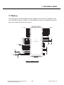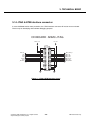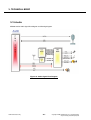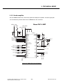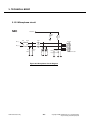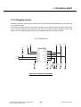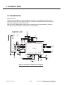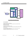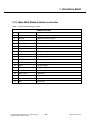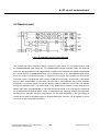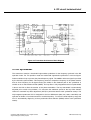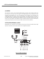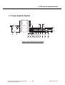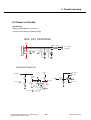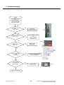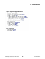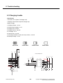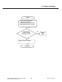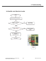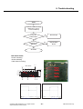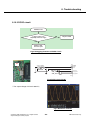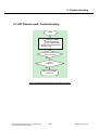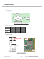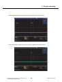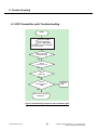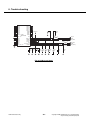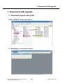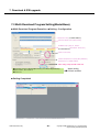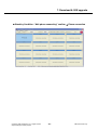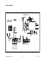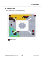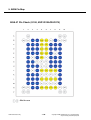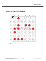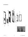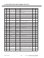
1
Service Manual
Internal Use Only
Service Manual
KM380t
Model : KM380t
Date: May, 2008 / Issue 1.0
REVISED HISTORY
Editor
Date
Issue
Contents of Changes
S/W Version
C.G.KANG
Mar. 5 2007
0.1
-
V08d
C.G.KANG
Apr. 10 2007
0.2
-
V10a
* The information in this manual is subject to change without notice and should not be construed as a
commitment by LGE Inc. Furthermore, LGE Inc. reserves the right, without notice, to make changes to
equipment design as advances in engineering and manufacturing methods warrant.
* This manual provides the information necessary to install, program, operate and maintain the
KM380t Series.
Copyright © 2008 LG Electronics. Inc. All right reserved.
Only for training and service purposes
-3-
LGE Internal Use Only
LGE Internal Use Only
-4-
Copyright © 2008 LG Electronics. Inc. All right reserved.
Only for training and service purposes
Table Of Contents
1. INTRODUCTION ...............................7
6. Trouble shooting............................64
1.1 Purpose .................................................. 7
1.2 Regulatory Information............................ 7
1.3 ABBREVIATION ..................................... 9
6.1 Trouble shooting test setup....................64
6.2 Power on Trouble...................................65
6.3 Charging trouble ....................................68
6.4 LCD display trouble................................70
6.5 Camera Trouble .....................................72
6.6 Receiver & Speaker trouble ...................74
6.7 Microphone trouble ................................76
6.8 Ear-MIc Jack Detection trouble..............77
6.9 Vibrator trouble ......................................78
6.10 Keypad back light trouble.....................79
6.11 SIM & uSD trouble ...............................80
6.12 RF Troubleshooting .............................83
6.13 RF Receiver path Troubleshooting ......85
6.14 RF Transmitter path Troubleshooting ..90
6.15 PAM Circuit ..........................................92
2. PERFORMANCE .............................11
2.1 H/W Features.........................................11
2.2 Technical specification...........................12
3. TECHNICAL BRIEF ........................19
3.1 KM380t series Component
Block diagram... ........................................19
3.2 Baseband Processor (BBP)
Introduction ............................................20
3.3 Power management IC ..........................30
3.4 Power ON/OFF ......................................34
3.5 SIM interface..........................................35
3.6 Micro SD external memory Interface .....36
3.7 Memory ..................................................37
3.8 LCD Display ...........................................38
3.9 Keypad Switching & Scanning ...............40
3.10 Keypad back-light illumination .............41
3.11 LCD back light illumination...................42
3.12 ISP(Image Signal Processor)...............43
3.13 Battery current consumption monitor ...44
3.14 JTAG & ETM interface connector ........45
3.15 Audio....................................................46
3.16 Charging circuit ....................................49
3.17 BLUETOOTH .......................................50
3.18 FM Radio .............................................52
3.19 18pin Multi Media Interface
connector .............................................53
4. RF circuit technical brief ...............55
4.1 General Description ...............................55
4.2 Receiver part..........................................57
4.3 Transmitter part......................................58
4.4 RF synthesizer .......................................59
4.5 DCXO.....................................................60
4.6 Front End Module control.......................60
4.7 Power Amplifier Module .........................61
5. PCB layout......................................62
7. Download & S/W upgrade.................95
7.1 Download program user guide...............95
7.2 Multi-Download Program Setting ...........96
8. CIRCUIT DIAGRAM ........................99
9. BGM PIN MAP...............................105
10. PCB LAYOUT ..............................111
11. RF Calibration.............................113
11.1 Test Equipment Setup .......................113
11.2 Calibration Step .................................113
12. Stand-alone Test ........................119
12.1 Test Program Setting .........................119
12.2 Tx Test ...............................................121
12.3 Rx Test...............................................122
13. ENGINEERING MODE ................123
14. EXPLODED VIEW &
REPLACEMENT PART LIST ......125
14.1 Exploded View ...................................125
14.2 Replacement Parts ............................127
14.3 Accessory ..........................................147
5.1 Main PCB component placement ..........62
Copyright © 2008 LG Electronics. Inc. All right reserved.
Only for training and service purposes
-5-
LGE Internal Use Only
LGE Internal Use Only
-6-
Copyright © 2008 LG Electronics. Inc. All right reserved.
Only for training and service purposes
1. INTRODUCTION
1. INTRODUCTION
1.1 Purpose
This manual provides the information necessary to repair, calibration, description and download the
features of the KM380t Series.
1.2 Regulatory Information
A. Security
Toll fraud, the unauthorized use of telecommunications system by an unauthorized part (for example,
persons other than your company’s employees, agents, subcontractors, or person working on your
company’s behalf) can result in substantial additional charges you’re your telecommunications
services. System users are responsible for the security of own system. There are may be risks of toll
fraud associated with your telecommunications system. System users are responsible for
programming and configuring the equipment to prevent unauthorized use. LGE does not warrant that
this product is immune from the above case but will prevent unauthorized use of common-carrier
telecommunication service of facilities accessed through or connected to it. LGE will not be
responsible for any charges that result from such unauthorized use.
B. Incidence of Harm
If a telephone company determines that the equipment provided to customer is faulty and possibly
causing harm or interruption in service to the telephone network, it should disconnect telephone
service until repair can be done. A telephone company may temporarily disconnect service as long as
repair is not done.
C. Changes in Service
A local telephone company may make changes in its communications facilities or procedure. If these
changes could reasonably be expected to affect the use of the KM380t Series or compatibility with the
network, the telephone company is required to give advanced written notice to the user, allowing the
user to take appropriate steps to maintain telephone service.
D. Maintenance Limitations
Maintenance limitations on the KM380t Series must be performed only at the LGE or its authorized
agents. The user may not make any changes and/or repairs expect asspecifically noted in this manual.
Therefore, note that unauthorized alternations or repair may affect the regulatory status of the system
and may void any remaining warranty.
Copyright © 2008 LG Electronics. Inc. All right reserved.
Only for training and service purposes
-7-
LGE Internal Use Only
1. INTRODUCTION
E. Notice of Radiated Emissions
The KM380t Series complies with rules regarding radiation and radio frequency emission as defined
by local regulatory agencies. In accordance with these agencies, you may be required to provide
information such as the following to the end user.
F. Pictures
The pictures in this manual are for illustrative purposes only; your actual hardware may look slightly
different.
G. Interference and Attenuation
An KM380t Series may interfere with sensitive laboratory equipment, medical equipment, etc.
Interference from unsuppressed engines or electric motors may cause problems.
H. Electrostatic Sensitive Devices
ATTENTION
Boards, which contains Electrostatic Sensitive Device(ESD), are indicated by the sign.
Following information is ESD handling: Service personnel should ground themselves by using a wrist
strap when exchange system boards.
When repairs are made to a system board, they should spread the floor with anti-static mat which is
also grounded. Use a suitable, grounded soldering iron. Keep sensitive parts in these protective
packages until these are used. When returning system boards or parts such as EEPROM to the
factory, use the protective package as described.
LGE Internal Use Only
-8-
Copyright © 2008 LG Electronics. Inc. All right reserved.
Only for training and service purposes
1. INTRODUCTION
1.3 ABBREVIATION
For the purposes of this manual, following abbreviations apply:
APC
Automatic Power Control
BB
Baseband
BER
Bit Error Ratio
CC-CV
Constant Current - Constant Voltage
CLA
Cigar Lighter Adapter
DAC
Digital to Analog Converter
DCS
Digital Communication System
dBm
dB relative to 1 milli-watt
DSP
Digital Signal Processing
EEPROM
Electrical Erasable Programmable Read-Only Memory
EGPRS
Enhanced General Packet Radio Service
EL
Electroluminescence
ESD
Electrostatic Discharge
FPCB
Flexible Printed Circuit Board
GMSK
Gaussian Minimum Shift Keying
GPIB
General Purpose Interface Bus
GPRS
General Packet Radio Service
GSM
Global System for Mobile Communications
IPUI
International Portable User Identity
IF
Intermediate Frequency
LCD
Liquid Crystal Display
LDO
Low Drop Output
LED
Light Emitting Diode
Copyright © 2008 LG Electronics. Inc. All right reserved.
Only for training and service purposes
-9-
LGE Internal Use Only
1. INTRODUCTION
LGE
LG Electronics
OPLL
Offset Phase Locked Loop
PAM
Power Amplifier Module
PCB
Printed Circuit Board
PGA
Programmable Gain Amplifier
PLL
Phase Locked Loop
PSTN
Public Switched Telephone Network
RF
Radio Frequency
RLR
Receiving Loudness Rating
RMS
Root Mean Square
RTC
Real Time Clock
SAW
Surface Acoustic Wave
SIM
Subscriber Identity Module
SLR
Sending Loudness Rating
SRAM
Static Random Access Memory
STMR
Side Tone Masking Rating
TA
Travel Adapter
TDD
Time Division Duplex
TDMA
Time Division Multiple Access
UART
Universal Asynchronous Receiver/Transmitter
VCO
Voltage Controlled Oscillator
VCTCXO
Voltage Control Temperature Compensated Crystal Oscillator
WAP
Wireless Application Protocol
8PSK
8 Phase Shift Keying
LGE Internal Use Only
- 10 -
Copyright © 2008 LG Electronics. Inc. All right reserved.
Only for training and service purposes
2. GENERAL PERFORMANCE
2. GENERAL PERFORMANCE
2.1 H/W Feature
Item
Standard Battery
Feature
Comment
Li-ion, 800mAh
AVG TCVR Current
tbd
@PL5
Standby Current
tbd
@PP9
Talk time
tbd
Standby time
Over 250 hours (Paging Period:9, RSSI: -85dBm)
Charging time
Under 3 hours
RX Sensitivity
EGSM: -105dBm↓, DCS/PCS: -105dBm↓
TX output power
EGSM : 32.5dBm (@PL 5)
DCS/PCS: 30/30dBm (@PL 0)
GPRS compatibility
Class 10
SIM card type
3V Small
Display
Status Indicator
Main 240 x 320 pixels, 2” ± QVGA, 265K color,
Navi, Send, Call End, Back and etc. Key are
implemented by touchpad.
CLEAR, SEND, END/PWR, MP3, AF/Camera double
action, Volume Up, Volume Down, Lock
ANT
EAR Phone Jack
PC Synchronization
Speech coding
Built in antenna
18pin multi port Headset jack (Call/Music)
3.5pi Stereo Jack. (Music Only)
Yes
HR/EFR/FR/AMR
Data and Fax
Yes
Vibrator
Yes
Buzzer
No
Voice Recoding
Yes
C-Mic
Yes
Receiver
Yes
Travel Adapter
Yes
Options
Bluetooth hands-free kit, Data Kit
Copyright © 2008 LG Electronics. Inc. All right reserved.
Only for training and service purposes
- 11 -
LGE Internal Use Only
2. GENERAL PERFORMANCE
2.2 Technical specification
Item
Description
Specification
GSM900
TX: 890 + 0.2 x n MHz
RX: 935 + 0.2 x n MHz ( n = 1 ~ 124 )
EGSM
TX: 890 + 0.2 x (n-1024) MHz
1
Frequency Band
RX: 935 + 0.2 x (n-1024) MHz ( n = 975 ~ 1023 )
DCS1800
TX: 1710 + ( n-511 ) x 0.2 MHz (n = 512 ~ 885)
RX: TX + 95 MHz
PCS1900
TX: 1850.2 + ( n-512 ) x 0.2 MHz (n = 512 ~ 810)
RX: TX + 80MHz
2
Phase Error
3
Frequency Error
RMS < 5 degrees
Peak < 20 degrees
< 0.1ppm
GSM900/EGSM
4
Power Level
LGE Internal Use Only
Level
Power
5
33 dBm
6
Toler.
Level
Power
Toler.
2dB
13
17 dBm
3dB
31 dBm
3dB
14
15 dBm
3dB
7
29 dBm
3dB
15
13 dBm
3dB
8
27 dBm
3dB
16
11 dBm
5dB
9
25 dBm
3dB
17
9 dBm
5dB
10
23 dBm
3dB
18
7 dBm
5dB
11
21 dBm
3dB
19
5 dBm
5dB
12
19 dBm
3dB
Level
Power
Toler.
DCS1800/PCS1900
Level
Power
0
30 dBm
2dB
8
14 dBm
3dB
1
28 dBm
3dB
9
12 dBm
4dB
2
26 dBm
3dB
10
10 dBm
4dB
3
24 dBm
3dB
11
8 dBm
4dB
4
22 dBm
3dB
12
6 dBm
4dB
5
20 dBm
3dB
13
4 dBm
4dB
6
18 dBm
3dB
14
2 dBm
5dB
7
16 dBm
3dB
15
0 dBm
5dB
- 12 -
Toler.
Copyright © 2008 LG Electronics. Inc. All right reserved.
Only for training and service purposes
2. GENERAL PERFORMANCE
Item
Description
Specification
GSM900/EGSM
5
Offset from Carrier (kHz).
Max. dBc
100
+0.5
200
-30
250
-33
400
-60
600 ~ 1,200
-60
1,200 ~ 1,800
-60
1,800 ~ 3,000
-63
3,000 ~ 6,000
-65
6,000
-71
Output RF Spectrum
(due to modulation)
DCS1800/PCS1900
Offset from Carrier (kHz).
Max. dBc
100
+0.5
200
-30
250
-33
400
-60
600 ~ 1,200
-60
1,200 ~ 1,800
-60
1,800 ~ 3,000
-65
3,000 ~ 6,000
-65
6,000
-73
GSM900/EGSM
6
Offset from Carrier (kHz)
Max. (dBm)
Output RF Spectrum
400
-19
(due to switching transient)
600
-21
1,200
-21
1,800
-24
Copyright © 2008 LG Electronics. Inc. All right reserved.
Only for training and service purposes
- 13 -
LGE Internal Use Only
2. GENERAL PERFORMANCE
Item
Description
Specification
DCS1800/PCS1900
6
7
8
Offset from Carrier (kHz).
Max. (dBm)
Output RF Spectrum
400
-22
(due to switching transient)
600
-24
1,200
-24
1,800
-27
Spurious Emissions
Bit Error Ratio
Conduction, Emission Status
EGSM
BER (Class II) < 2.439% @-102dBm
DCS1800/PCS1900
BER (Class II) < 2.439% @-100dBm
9
Rx Level Report accuracy
10
SLR
11
12
13
8
3 dB
Frequency (Hz)
Max.(dB)
Min.(dB)
100
-12
-
200
0
-
300
0
-12
1,000
0
-6
2,000
4
-6
3,000
4
-6
3,400
4
-9
4,000
0
-
Frequency (Hz)
Max.(dB)
Min.(dB)
100
-12
-
200
0
-
300
2
-7
500
*
-5
1,000
0
-5
3,000
2
-5
3,400
2
-10
4,000
2
Sending Response
RLR
2 3 dB
Receiving Response
* Mean that Adopt a straight line in between 300 Hz
and 1,000 Hz to be Max. level in the range.
LGE Internal Use Only
- 14 -
Copyright © 2008 LG Electronics. Inc. All right reserved.
Only for training and service purposes
2. GENERAL PERFORMANCE
Item
Description
Specification
14
STMR
13 5 dB
15
Stability Margin
> 6 dB
16
dB to ARL (dB)
Level Ratio (dB)
-35
17.5
-30
22.5
-20
30.7
-10
33.3
0
33.7
7
31.7
10
25.5
Distortion
17
Side Tone Distortion
Three stage distortion < 10%
18
System frequency
(26 MHz) tolerance
2.5ppm
19
32.768KHz tolerance
30ppm
20
Power consumption
21
Talk Time
22
Standby Time
23
Ringer Volume
24
Charge Current
Standby
- Normal
3 mA(@PP9)
EGSM/Lvl 7 (Battery Capacity 800mA):180 min
EGSM/Lvl12(Battery Capacity 800 mA):320min
Under conditions, at least 300 hours:
1. Brand new and full 800mAh battery
2. Full charge, no receive/send and keep GSM in idle mode.
3. Broadcast set off.
4. Signal strength display set at 3 level above.
5. Backlight of phone set off.
At least 65 dB under below conditions:
1. Ringer set as ringer.
2. Test distance set as 50 cm
Fast Charge : < 400 mA
Slow Charge: < 120 mA
Antenna Bar Number
25
Antenna Display
Copyright © 2008 LG Electronics. Inc. All right reserved.
Only for training and service purposes
- 15 -
Power
7
>-92 dBm ~
5
-97dBm ~ -93dBm
4
-100dBm ~ -98dBm
2
-103dBm ~ -101dBm
1
-105dBm ~ -104dBm
0
< -106 dBm
Off
No Service
LGE Internal Use Only
2. GENERAL PERFORMANCE
Item
26
Description
Specification
Battery Bar Number
Voltage( 0.05V)
3
3.69V ~ 4.2V
2
3.53V ~ 3.69V
1
3.43V ~ 3.53V
0
3.30V ~ 3.43V
Battery Indicator
3.53V↓
0.05V (Call)
3.43V↓
0.05V (Standby)
27
Low Voltage Warning
28
Forced shut down Voltage
3.3
Battery Type
Li-ion Battery or Li-Polymer Battery
Standard Voltage = 3.7 V
Battery full charge voltage = 4.2 V
Capacity: 800mAh
Travel Charger
Switching-mode charger
Input: 100 ~ 240 V, 50/60Hz
Out put: 4.8, 0.9A
29
31
LGE Internal Use Only
0.05 V
- 16 -
Copyright © 2008 LG Electronics. Inc. All right reserved.
Only for training and service purposes
2. GENERAL PERFORMANCE
* EDGE RF Specification (Option: is not serviced for “EDGE mode”)
Item
1
2
3
4
Description
RMS EVM
Peak EVM
95th Percentile EVM
Origin Offset Suppression
Specification
≥
9%
30%
15%
30dB
GSM900/EGSM
5
Power Level
Level
Power
Toler.
Level
Power
Toler.
5
27dBm
3dB
13
17dBm
3dB
6
27dBm
3dB
14
15dBm
3dB
7
27dBm
3dB
15
13dBm
3dB
8
27dBm
3dB
16
11dBm
5dB
9
25dBm
3dB
17
9dBm
5dB
10
23dBm
3dB
18
7dBm
5dB
11
21dBm
3dB
19
5dBm
5dB
12
19dBm
3dB
Level
Power
Toler.
DCS1800, PCS1900
6
Output RF Spectrum
(due to modulation)
Copyright © 2008 LG Electronics. Inc. All right reserved.
Only for training and service purposes
Level
Power
Toler.
0
26/25dBm
3dB
8
14 dBm
3dB
1
26/25dBm
3dB
9
12 dBm
4dB
2
26/25dBm
3dB
10
10 dBm
4dB
3
24 dBm
3dB
11
8 dBm
4dB
4
22 dBm
3dB
12
6 dBm
4dB
5
20 dBm
3dB
13
4 dBm
4dB
6
18 dBm
3dB
14
2 dBm
5dB
7
16 dBm
3dB
15
0 dBm
5dB
GSM900/EGSM
Offset from carrier(kHz)
Max. dBc
100
+0.5
200
-30
250
-33
400
-54
600 ~ <1,200
-60
1,200 ~ <1,800
-60
1,800 ~ <3,000
-63
3,000 ~ <6,000
-65
6,000
-71
- 17 -
LGE Internal Use Only
2. GENERAL PERFORMANCE
Item
6
Description
Output RF Spectrum
(due to modulation)
7
Output RF Spectrum
(due to switching transient)
Specification
DCS1800, PCS1900
Offset from carrier(kHz)
Max. dBc
100
+0.5
200
-30
250
-33
400
-54
600 ~ <1,200
-60
1,200 ~ <1,800
-60
1,800 ~ <3,000
-63
3,000 ~ <6,000
-65
6,000
-71
GSM900/EGSM
Offset from carrier(kHz)
Max. dBm
400
-23
600
-26
1,200
-27
1,800
--30
DCS1800, PCS1900
LGE Internal Use Only
Offset from carrier(kHz)
Max. dBm
400
-23
600
-26
1,200
-27
1,800
-30
- 18 -
Copyright © 2008 LG Electronics. Inc. All right reserved.
Only for training and service purposes
3. TECHNICAL BRIEF
3. TECHNICAL BRIEF
3.1 KM380t series Component Block diagram
Figure 1. KM380t series Functional Block Diagram
Copyright © 2008 LG Electronics. Inc. All right reserved.
Only for training and service purposes
- 19 -
LGE Internal Use Only
3. TECHNICAL BRIEF
3.2 Baseband Processor (BBP) Introduction
S-GOLDradi o
Baseband
GS
Cip her
IS/
IR-Memor y
R
TEAKLit Æ
FIR
DAC
X
U
M
Speech
and
Deco din
DAC
Equ alize
DigR
USB FS
SRAM
FCDP
Keypad
DMAC
ICU
GPIO
USI
GS
Timer
RF
Contr o
SCCU
EBU
GEA-1/2/3
CGU
CAPCOM
AUX
ADC
RTC
IrDA
MMC/SD
I
MOVE
USIM
I
USARTs
LPF
+
GPT
ARMÆ926
AD
Sigm a-Delta
MASH
Modula to
GMSK
8PSK
Speech
and
Encod in
AD
AD
DC
Offs et
Comp
FIR
Dig R
I C
JTAG
Multimed ia IC
Camera
I
Disp lay
I
3-wire
Ctrl
AD
L
Ramp
Gen
DCXO
DA
PA/FE
Con tro
LDO
Power
Handsfr ee
Am p
Powe
Con tro
LED
PWMís
Charger
S
(BL
PL
LD
RF
LD
GP
LD
VI
LD
SD1
(1.5V)
I/
LD
RF
LD
SI
LD
AUX
LD
SD2
(1.8V)
ANA
LD
RF1
LD
USB
LD
RTC
LD
Figure 3. Top level block diagram of the S-GOLDRadio™ (PMB8888)
3.2.1 General Description
S-GOLDRadio™ is a GSM/EDGE single chip mixed signal Single Chip Radio IC containing all analog
and digital functionality of a cellular radio. Additionally S-GOLDRadio™ Provides multimedia
extensions such as camera, software MIDI, MP3 sound. It is designed as a single chip solution,
integrating the digital and mixed signal portions of the base band in 0.13um, 1.5V technology.
The chip will fully support the FR/HR/EFR/NB-AMR speech codec. S-GOLDRadio™ support multi-slot
operation modes CSD/GPRS/EGPRS (up to class 12) without additional external hardware.
LGE Internal Use Only
- 20 -
Copyright © 2008 LG Electronics. Inc. All right reserved.
Only for training and service purposes
3. TECHNICAL BRIEF
3.2.2 Block Description
• Processing core
ARM926EJ-S 32 bit processor core for controller functions. The ARM926EJ-S includes an MMU,
and the Jazelle Java extension for Java acceleration.
- TEAKLite DSP core
• ARM-Memory
- 32k Byte Boot ROM on the AHB
- 96k Byte SRAM on the AHB, flexibly usable as program or data RAM
- 16k Byte Cache for Program (internal)
- 8k Byte tightly coupled memory for Program(internal)
- 8k Byte Cache for Data(internal)
- 8k Byte tightly coupled memory for Data(internal)
• DSP-Memory
- 104K x 16bit Program ROM
- 8k x 16bit Program RAM
- 60k x 16bit Data ROM
- 37k x 16bit Data RAM
- Incremental Redundancy(IR) Memory of 35904 words of 16bit
• Shared Memory Block
1.5K x 32bit Shared RAM(dual ported) between controller system and TEAKLite.
• Controller Bus system
The processor cores and their peripherals are connected by powerful buses. Multi-layer AHB for
connecting the ARM and the other master capable building blocks with the internal and external
memories and with the peripheral buses.
• Clock system
The clock system allows widely independent selection of frequencies for the essential parts of the
S-GOLD3. Thus power consumption and performance can be optimized for each application.
• Functional Hardware block
- CPU and DSP Timers
- MOVE coprocessor performing motion estimation for video encoding algorithms (H.263, MPEG-4)
- Programmable PLL with additional phase shifters for system clock generation
- GSM Timer Module that off-loads the CPU from radio channel timing
- GMSK / 8-PSK Modulator according to GSM-standard 05.04 (5/2000)
- GMSK Modulator: gauss-filter with B*T=0.3
- EDGE Modulator: 8PSK-modulation with linearized GMSK-Pulse-Filter
- Hardware accelerators for equalizer and channel decoding.
- Incremental Redundancy memory for EDGE class 12 support
- A5/1, A5/2, A5/3 Cipher unit
- GEA1, GEA2, GEA3 Cipher Unit to support GPRS data transmission
- Advanced static and dynamic power management features including TDMA-Frame synchronous
low power mode and enhanced CPU modes(idle and sleep modes)
Copyright © 2008 LG Electronics. Inc. All right reserved.
Only for training and service purposes
- 21 -
LGE Internal Use Only
3. TECHNICAL BRIEF
- Pulse Number Modulation output for Automatic Frequency Correction(AFC)
- Serial RF Control interface: support of direct conversion RF
- A Universal Serial Interface(USIF) enabling asynchronous (UART) of synchronous (SPI) serial
data transmission
-1 Serial Synchronous SPI compatible interfaces in the controller domain
- 1 Serial Synchronous SPI compatible interface in the TEAKLite domain
- 2 USART with autobaud detection, hardware flow control and integrated IrDA controller
supporting IrDA’s SIR standard (up to 115.2Kbps)
- A dedicated Fas IfDA Controller supporting IrDA’s SIR,MIR and FIR standards (up to 4Mbps)
- I2C-bus interface (e.g. connection to S/M power)
- A fast display interface supporting serial and parallel interconnection
- An ITU-R BT.656 compatible Camera interface.
- Programmable clock output for a camera
- An multimedia/Secure Digital Card Interface (MMCI/SD: SDIO capable)
3.2.3 External Devices connected to memory interface
Table 1. Memory interface
Device
Name
Maker
Remark
NAND FLASH
K5D1G12ACE-D075
Samsung
Synchronous / A synchronous
SDRAM
K5D1G12ACE-D075
Samsung
Synchronous 133MHz
LCD
IM200DBN7A
LGIT
8bit access 2times transmission
MP3 Decoder
TCC8720
Telechips
MP3 Decoder
3.2.4 RF Interface
S-GOLDRadio uses this interface to control RF IC and Peripherals. 13 signals are provided switch
on/off RF ICs Periodically each TDMA frame.
Table 2. RF Interface Spec.
Resource
Interconnection
Description
TX2
TXHB
Output High band(DCS/PCS) Tx
TX1
TXLB
Output Low band(850/900) Tx
RX1, RX1X
GSM850_RXP, GSM850_RXN
Input of GSM850 LNA
RX2, RX2X
GSM900_RXP, GSM900_RXN
Input of GSM900 LNA
RX3, RX3X
DCS1800_RXP, DCS1800_RXN
Input of DCS1800 LNA
RX4, RX4X
PCS1900_RXP, PCS1900_RXN
Input of PCS1900 LNA
PABS
PA_BAND
Select PAM operation band.
FE1, FE2
VC1, VC2
Control FEM operation band & mode
PAEN
PA_EN
PAM Enable
VRAMP
TX_RAMP
Tx Ramp signal
T_OUT6
PA_MODE_2
Select PAM operation mode (GSM/EDGE)
LGE Internal Use Only
- 22 -
Copyright © 2008 LG Electronics. Inc. All right reserved.
Only for training and service purposes
3. TECHNICAL BRIEF
3.2.5 USART Interface
KM380t have two UART Drivers as follow :
- USART0 : SW upgrade / Calibration
- USIF : BT Interface.
Table 3. USIF Interface Spec.
Resource
Name
Remark
UART0_TXD
UART_TX
Transmit Data
UART0_RXD
UART_RX
Receive Data
USIF_TXD
UART_BT_TX
Transmit Data
USIF_RXD
UART_BT_RX
Receive Data
T_OUT3
UART_BT_RTS
Flow Control Signal
T_OUT4
UART_BT_CTS
Flow Control Signal
UART0
USIF
3.2.6 ADC channel
BBP ADC block is composed of 7 external ADC channel. This block operates charging process and
other related process by reading battery voltage and other analog values.
Table 4. S-Gold3 ADC channel usage
ADC channel
Resource
Interconnection
Description
M0
BAT_ID
Battery temperature measure
M1
RF_TEMP
RF block temperature measure
M2
N.C
M3
N.C
M4
N.C
M5
N.C
M6
N.C
M7
N.C
M8
VBAT
Battery supply voltage measure
M9
LOAD
Current consumption measure
M10
N.C
Copyright © 2008 LG Electronics. Inc. All right reserved.
Only for training and service purposes
- 23 -
LGE Internal Use Only
3. TECHNICAL BRIEF
3.2.7 GPIO map
Over a hundred allowable resources, KM380t series is using as follows except dedicated to SIM and
Memory. KM380t series GPIO(General Purpose Input/Output) Map, describing application, I/O state,
and enable level, is shown in below table.
Table 5. S-GOLDRadio GPIO pin Map
Port Function
Net Name
Description
KEY MATRIX
KP_IN2
KP_IN(2)
KP_IN3
KP_IN(3)
KP_IN4
KP_IN(4)
KP_IN5
KP_IN(5)
KP_IN6
KP_IN(6)
KP_OUT0
KP_OUT(0)
KP_OUT1
KP_OUT(1)
KP_OUT2
KP_OUT(2)
KP_OUT3
KP_OUT(3)
DSPIN1
KP_OUT(4)
UART0
UART0_RXD
UART_RX
UART, RS232 Data
UART0_TXD
UART_TX
UART, RS232 Data
UART0_RTS_N
uSD_DET
Micro SD Card Detect
UART0_CTS_N
MM_RESET
MP3 Decoder Reset
USIF
USIF_TXD_MTSR
UART_BT_TX
USIF_RXD_MRST
UART_BT_RX
TOUT_3
UART_BT_RTS
Bluetooth RTS
TOUT_4
UART_BT_CTS
Bluetooth CTS
USB_DPLUS
USB_BB_DP
USB +
USB_DMINUS
USB_BB_DM
USB -
CLK32K
For FM Radio, BT CLK32K
USB
CLK
DSPIN0
LGE Internal Use Only
- 24 -
Copyright © 2008 LG Electronics. Inc. All right reserved.
Only for training and service purposes
3. TECHNICAL BRIEF
CAMERA I/F
CIF_D0
CAM_D(0)
Camera DATA[0]
CIF_D1
CAM_D(1)
Camera DATA[1]
CIF_D2
CAM_D(2)
Camera DATA[2]
CIF_D3
CAM_D(3)
Camera DATA[3]
CIF_D4
CAM_D(4)
Camera DATA[4]
CIF_D5
CAM_D(5)
Camera DATA[5]
CIF_D6
CAM_D(6)
Camera DATA[6]
CIF_D7
CAM_D(7)
Camera DATA[7]
CIF_PCLK
CAM_PCLK
Camera pixel clock
CIF_HSYNC
CAM_HS
Camera H sync
CIF_VSYNC
CAM_VS
Camera V sync
CLKOUT
CAM_MCLK
Camera main clock
CIF_PD
CAM_PD
Camera power down(active high)
CIF_RESET
CAM_RESET
Camera reset
DIF_D0
DIF_D(0)
LCD data[0]
DIF_D1
DIF_D(1)
LCD data[1]
DIF_D2
DIF_D(2)
LCD data[2]
DIF_D3
DIF_D(3)
LCD data[3]
DIF_D4
DIF_D(4)
LCD data[4]
DIF_D5
DIF_D(5)
LCD data[5]
DIF_D6
DIF_D(6)
LCD data[6]
DIF_D7
DIF_D(7)
LCD data[7]
DIF_D8
DIF_D(8)
LCD data[8]
DIF_CS1
DIF_CS
LCD chip select
DIF_CS2
EHI_INT
MP3 Decoder Interrupt
DIF_CD
DIF_RS
Command Data switch
DIF_WR
DIF_WR
LCD Write
DIF_HD
EOC
Indicating End of Charging.
DIF_VD
LCD_VSYNC
VSYNC
DIF_RESET2
JACK_DET_3.5
Detect plug-in of 3.5pi Ear-Phone
I2C_SCL
I2C_SCL
For Sub-PMIC/Audio DAC/Camera
I2C_SDA
I2C_SDA
For Sub-PMIC/Audio DAC/Camera
LCD I/F
I2C
Copyright © 2008 LG Electronics. Inc. All right reserved.
Only for training and service purposes
- 25 -
LGE Internal Use Only
3. TECHNICAL BRIEF
SIM I/F
CC_IO
SIM_IO
SIM CARD I/O
CC_CLK
SIM_CLK
SIM CARD CLOCK
CC_RST
SIM_RST
SIM CARD RESET
I2S1
I2S1_CLK0
Not used
I2S1_RX
Not used
I2S1_TX
Not used
I2S1_WA0
Not used
External Memory
MMCI_CMD
RPWRON
Remote Power On
MMCI_DAT[0]
uSD_DET_CTRL
uSD Card Detect
MMCI_CLK
TF_CLK
T-flash
MMCI_DAT[1]
BT_INT
BT Interrupt
MMCI_DAT[2]
FLIP_OPEN
Flip Open/Close Detect
MMCI_DAT[3]
HOLD
HOLD Key
EP_N, EP_P
SPK_N, SPK_P
For Speaker
HS_N, HS_P
RCV_N, RCV_P
For Receiver
EPPA1
BBP_SND_L
For Speaker
Audio I/F
EPREF
Reference
EPPA2
BBP_SND_R
For Speaker
MICN1
MIC_N
For Mic
MICP1
MIC_P
For Mic
MICN2
HS_MIC_N
For Headset Mic
MICP2
HS_MIC_P
For Headset Mic
VMIC
MICBIAS
Power for MIC
M0
BAT_ID
Battery temperature measure
M1
RF_TEMP
RF block temperature measure
M7
H/W VERSION
S-GOLDRadio H/W version detect
M8
VSUPPLY
Battery supply voltage measure
M9
LOAD
Current consumption measure
M10
N.C
ADC
M2
M3
LGE Internal Use Only
- 26 -
Copyright © 2008 LG Electronics. Inc. All right reserved.
Only for training and service purposes
3. TECHNICAL BRIEF
Reference
VREF
IREF
JTAG I/F
TDO
TDO
JTAG
TDI
TDI
JTAG
TMS
TMS
JTAG
TCK
TCK
JTAG
TRST_n
_TRST
JTAG
RTCK
RTCK J
TAG
Memory
EBU_AD[0]
DATA(0)
EBU _AD[1]
DATA (1)
EBU _AD[2]
DATA (2)
EBU _AD[3]
DATA (3)
EBU _AD[4]
DATA (4)
EBU _AD[5]
DATA (5)
EBU _AD[6]
DATA (6)
EBU _AD[7]
DATA (7)
EBU _AD[8]
DATA (8)
EBU _AD[9]
DATA (9)
EBU _AD[10]
DATA (10)
EBU _AD[11]
DATA (11)
EBU _AD[12]
DATA (12)
EBU _AD[13]
DATA (13)
EBU _AD[14]
DATA (14)
EBU _AD[15]
DATA (15)
EBU _WR_N
_WR
EBU _RD_N
_RD
EBU _BC0_N
_BC0
EBU _BC1_N
_BC1
EBU _A[0]
ADD(0)
EBU _A[1]
ADD (1)
EBU _A[2]
ADD (2)
EBU _A[3]
ADD (3)
EBU _A[4]
ADD (4)
Copyright © 2008 LG Electronics. Inc. All right reserved.
Only for training and service purposes
- 27 -
LGE Internal Use Only
3. TECHNICAL BRIEF
EBU _A[5]
ADD (5)
EBU _A[6]
ADD (6)
EBU _A[7]
ADD (7)
EBU _A[8]
ADD (8)
EBU _A[9]
ADD (9)
EBU _A[10]
ADD (10)
EBU _A[11]
ADD (11)
EBU _A[12]
ADD (12)
EBU _A[13]
ADD (13)
EBU _A[14]
ADD (14)
EBU _A[15]
ADD (15)
EBU _A[16]
ADD (16)
EBU _A[17]
ADD (17)
EBU _A[18]
ADD (18)
EBU _A[19]
ADD (19)
EBU _A[20]
ADD (20)
EBU _A[21]
ADD (21)
EBU _A[22]
ADD (22)
EBU _A[23]
ADD (23)
EBU _A[24]
ADD (24)
EBU _CS0_n
_FLASH1_CS
EBU _CS1_n
SDRAM_CS
EBU _CS2_n
nCS1
EBU _CS3_n
EBU _ADV_n
EBU _RAS_n
_RAS
EBU _CAS_n
_CAS
EBU _WAIT_n
EBU _SDCLKO
SDCLKO
EBU _SDCLKI
SDCLKI
EBU _BFCLKO
EBU _BFCLKI
EBU _CKE
CKE
Memory
FCDP_RBn
LGE Internal Use Only
FCDP
- 28 -
Copyright © 2008 LG Electronics. Inc. All right reserved.
Only for training and service purposes
3. TECHNICAL BRIEF
TDMA I/F
T_OUT3
UART_BT_RTS
T_OUT4
UART_BT_CTS
T_OUT5
CHG_EN
T_OUT6
PA_MODE_2
T_OUT7
HOOK_DETECT
T_OUT8
VBUS_OVP
PAM
USB DETECT
System Port
CLKOUT0 [<=26MHz]
F26M
Not used
26MHZ_MCLK
26M Main Clock
F32K
to 32k crystal
OSC32K
to 32k crystal
RESET_n
_RESET
TRIG_OUT
TRIG_OUT
RTC_OUT
RTC_OUT
Copyright © 2008 LG Electronics. Inc. All right reserved.
Only for training and service purposes
- 29 -
LGE Internal Use Only
3. TECHNICAL BRIEF
3.3 Power management IC
3.3.1 General Description
S-GOLDradio has a highly integrated Power and Battery Management block for mobile handsets.
Block Description
• Highly efficient step-down converter for main digital baseband supply including Core, DSP and
memory interface (External Bus Unit).
• Support of S-GOLD standby power-down concept
• Low-drop-out (LDO) regulators for Flash and mobile RAM memory devices
• Voltage independent switching of two SIM cards
• LDO regulators for baseband I/O supply
• LDO regulator for analog mixed-signal section of S-GOLD
• Low-noise LDO regulators for RF devices
• Supply for Bluemoon Single, Infineon’s single chip solution for Bluetooth
• Audio amplifier 8 Ohms for handsfree operation and ringing
• Charge Control for charging Li-Ion/Polymer batteries under software control
• Pre-charge current generator with selectable current level
• RTC regulator with ultra-low quiescent current
• USB interface support for peripheral and mini-host mode
• Vibrator driver with adjustable voltage
• Fully controlable by software via I2C - Bus
• Temperature and battery voltage sensors
• Interrupt channels for peripherals
LGE Internal Use Only
- 30 -
Copyright © 2008 LG Electronics. Inc. All right reserved.
Only for training and service purposes
3. TECHNICAL BRIEF
Figure 4. Top level block diagram of the PMU Block of PMB8888
Copyright © 2008 LG Electronics. Inc. All right reserved.
Only for training and service purposes
- 31 -
LGE Internal Use Only
3. TECHNICAL BRIEF
Table 6. LDO Output Table of SM-Power
LDO
Net name
Output Voltage Output Current
Usage
SD1
VSD1_1V5
1.5V
700mA
Core & for LDO
SD2
VSD2_1V8
1.8V
700mA
Memory
VAUX
VBT_2V9
2.9V
400mA
BT Power
VIO
VIO_2V62
2.62V
300mA
Peripherals
VSIM
VSIM_2V9
2.9V
150mA
SIM card
VMME
-
2.9V
150mA
Not used
VAUDIO
VAUDIO_2V5
2.5V
620mA
VUSB
VUSB_3V1
3.1V
262mA
VRF1
VRF1_2V85
2.85V
200mA
VRF2
VRF2_1V5
1.5V
240mA
VRF3
VRF3_2V85
2.85V
470mA
VPLL
VPLL_1V5
1.5V
150mA
S-GOLDRadio PLL
VRTC
VRTC_2V0
2.0V
20mA
RTC
VVIB
VVIB_2V8
2.8V
450mA
VUSB_3V1
VRF3_2V85
VRF3_2V85
VRF3_2V85
USB Switch
VAUDIO_2V5
VBAT
C109
100p
22p
C111
10n
C113
10n
0.1u
C112
C114
0.1u
C102
1u
0.47u
VPLL_1V5
1u
C100
2.2u
C110
0.1u
VRF2_1V5
C101
VVIB_2V8
KDR331V
2.2u
L100
47nH
2
VCHG_OVP
1
VBUS_OVP
3
C103
C108
L102
47nH
C104
VRF1_2V85 VRF3_2V85
VRF3_2V85
L101
47nH
VBT_2V9
C107
1u
D100
C115
1u
C105
2.2u
0.1uF C106
VRTC_2V0
VIO_2V62
VRF1_2V85
VRF3_2V85
VBAT
VRTC_2V0
VSIM_2V9
C118 0.1uF
C592
1u
C119
100p
C121
1u
C117
C122
1u
2.2u
C120
0.1u
C123
220n
C124
VBAT
C125
1u
0.1u
VRF2_1V5
TP105
4.7K
R110
100K
R109
LOAD
TXHB
TXLB
GSM850_RXP
GSM850_RXN
GSM900_RXP
GSM900_RXN
W3
V3
W2
V1
U1
T1
R3
R4
M0
M1
M2
M7
M8
M9
M10
TX2
TX1
RX1
RX1X
RX2
RX2X
PABIAS
E18
VSS_RTC
D18
VDD_RTC
M4
A1
NC1
A19
NC2
W19
NC3
A4
C5
D5
C4
D7
A5
C8
C3
M2
N2
N3
P2
R2
T2
U2
U3
U6
V2
V4
V5
V6
W1
VSS_LDO3
VSSRF1
VSSRF2
VSSRF3
VSSRF4
VSSRF5
VSSRF6
VSSRF7
VSSRF8
VSSRF9
VSSRF10
VSSRF11
VSSRF12
VSSRF13
VSSRF14
E1
E2
E3
C10
D11
D12
E12
E11
A7
B7
C6
C7
A8
B8
D6
A3
B4
B3
A2
B1
B2
V7
VDDXO
W6
VDDPLL
L1
VDDRX
T6
VDDDIG
P4
VDDMS
W4
VDDTX
W5
VDDVCO
T3
VDDTRX
VDD_FUSE_FS
H3
J3
G4
H4
G3
J4
F4
CH_SOURCE
CH_GATE
SENSE_IN1
SENSE_IN2
VDD_REF
VDDCHARGE
CHARGE_UC_SCAN_IN1
BAT_ID
RF_TEMP
V19
C128
0.1uF
VAUDIO
VBAT_AUDIO
VSS_AUDIO
VLED
VAUX
VVIB
VBAT_LDO1
VSS_LDO1
VMMC
VUSB
VBAT_BSW_USB_MMC
VIO
VSIM
VBAT_LDO2
VSS_LDO2
VPLL
VRF2
VDD_RF2PLL
VRF1
VRF3
VBAT_RF13
390K
R105
VBAT
F3
VSS_MS
H2
VSS_EP
K1
AGND_MS1
K4
AGND_MS2
C127
0.1uF
VDDP_EBU_1
C126
0.1uF
L12
VSS_MAIN_1
L10
VSS_MAIN_2
M10
VSS_MAIN_3
J8
VSS_MAIN_4
L8
VSS_MAIN_5
VSD1_1V5
L11
VDD_MAIN_1
M11
VDD_MAIN_2
L9
VDD_MAIN_3
M9
VDD_MAIN_4
VSD2_1V8
DATA(0:15)
EBU_AD0
EBU_AD1
EBU_AD2
EBU_AD3
EBU_AD4
EBU_AD5
EBU_AD6
EBU_AD7
EBU_AD8
EBU_AD9
EBU_AD10
EBU_AD11
EBU_AD12
EBU_AD13
R14
W18
V18
W17
T15
U14
V17
T14
R13
W16
V16
U12
W15
W14
V15
TP101
Figure 6. LDOs Circuit Diagram of KM380t series
LGE Internal Use Only
- 32 -
Copyright © 2008 LG Electronics. Inc. All right reserved.
Only for training and service purposes
3. TECHNICAL BRIEF
3.3.2 Charging
KM380t charge the battery using an external charging IC of Intersil ISL9221 for Li-Ion or Li-Polymer
battery in 4.2 Volts level.
4.2V~3.69V
3.69V~3.53V
3.53V~3.43V
3.43V~3.3V
Figure 7. Battery Block Indication
1 Charging method : CC-CV
2 Charger detect voltage : 4.0 V
3 Charging time : 2h 30m
4 Charging current : 400 mA
5 CV voltage : 4.2 V
6 Cutoff current : 110 mA
7 Full charge indication current (icon stop current) : 110 mA
8 Recharge voltage : 4.16 V
9 Low battery alarm
a. Idle : 3.45 V ~ 3.35 V
b. Dedicated : 3.45 V ~ 3.35 V
10. Low battery alarm interval
a. Idle : 3 min
b. Dedicated : 1 min
11. Switch-off voltage : 3.35 V
12. Charging temperature adc range
a. ~ -5 : low charging voltage operation (3.6 V ~ 3.9 V)
b. -5 ~ 50 : standard charging (up to 4.2 V)
c. 50 ~ : low charging voltage operation (3.6V ~ 3.9V)
Copyright © 2008 LG Electronics. Inc. All right reserved.
Only for training and service purposes
- 33 -
LGE Internal Use Only
3. TECHNICAL BRIEF
3.4 Power ON/OFF
KM380t series Power State : Defined 3cases as follow
] Power -ON : Power key detect (S-GOLDradio PWRON port)
] Power -ON-charging : Charger or USB detect.
Remote Power On
VRTC_2V0
END_KEY_IN
RPWRON_EN
2K
R432
2K
R535
KP_IN(6)
R431
330K
R435
END
10K
100K
R534
C410
10u
1
2
3
6
5
4
R436
RPWRON
100K
PWRON
R434
3.3M
KP_OUT(2)
Q400
EMX18
END_KEY_IN
Figure 8. Remote power on and End-key power on circuit
Input ON is a power-on input for S-GOLDradio with 2 active high levels (see Figure 8). It might be
triggered by a push button. To detect if the push-button is pressed during system operation the logical
level at pin ON or its change (if Bit 1 EION in INTCTRL2 is asserted) is recorded in bit LON of the ISF
register. If the high level of voltage at pin ON does not reach VIHdet (Vbat-0.8 ~ Vbat-0.3) the abovementioned bit won’t be set.
To support Remote power on function for factory mass production, applied an BJT as following figure.
As monitoring the RPWRON and Key matrix KP_OUT(2) & KP_IN(6), KM380t series system recognize
whether remote power on or End-key pushed
LGE Internal Use Only
- 34 -
Copyright © 2008 LG Electronics. Inc. All right reserved.
Only for training and service purposes
3. TECHNICAL BRIEF
3.5 SIM interface
KM380t supports 1.8V & 3V plug in SIM, SIM interface scheme is shown in (Figure 10). SIM_IO,
SIM_CLK, SIM_RST ports are used to communicate with BBP(S-GOLDRadio) and the SIM
powersupply enabled by BBP (_SIM_EN).
SIM Interface
SIM_CLK: SIM card reference clock
SIM_RST: SIM card Async /sync reset
SIM_IO: SIM card bidirectional reset
VSIM_2V9
J301
R325
10K
SIM_IO
C346
22p
9
10
6
5
4
8
GND3 GND2
7
GND4 GND1
3
C7
C3
2
C6
C2
1
C5
C1
SIM_CLK
SIM_RST
C347
0.1u
C348
150p
Figure 9. SIM Circuit
Copyright © 2008 LG Electronics. Inc. All right reserved.
Only for training and service purposes
- 35 -
LGE Internal Use Only
3. TECHNICAL BRIEF
3.6 Micro SD external memory Interface
In KM380t series a Micro SD slot for external Memory is connected to MP3 Decoder TCC8720.
2V8_VMM
uSD CARD
56K
56K
R237
47K
R236
47K
R235
56K
R234
56K
R233
R232
100K
R231
VIO_2V62
S1
SWA
uSD_DET
uSD_D1
uSD_D0
DM3AT-SF-PEJ
SWB
8
7
6
5
4
3
2
1
uSD_CLK
uSD_CMD
uSD_D3
uSD_D2
C245
1000 pF
C246
10p
C247
1u
GND
Figure 10. Micro SD Card Circuit
Micro SD memory pad assign.
SD mode
Pin No.
Name
Type
Description
1
uSD_DAT2
I/O
Data bit [2]
2
uSD_DAT3
I/O
Data bit [3]
3
uSD_CMD
I/O
Command response
4
2V8_VMM
Power
Power supply
5
uSD_CLK
I
Clock
6
VSS
Ground
Power ground
7
uSD_DAT0
I/O
Data bit [0]
8
uSD_DAT1
I/O
Data bit [1]
LGE Internal Use Only
- 36 -
Copyright © 2008 LG Electronics. Inc. All right reserved.
Only for training and service purposes
3. TECHNICAL BRIEF
3.7 Memory
1Gbit NAND Flash & 512Mbit SDRAM employed on KM380t series with 8 bit bus for NAND and 16bit
bus for SDRAM thru ADD(0) ~ ADD(24). The 1Gbit NAND Flash memory with SDRAM stacked device
DATA(0:15)
DATA(0)
DATA(1)
DATA(2)
DATA(3)
DATA(4)
DATA(5)
DATA(6)
DATA(7)
DATA(8)
DATA(9)
DATA(10)
DATA(11)
DATA(12)
DATA(13)
DATA(14)
DATA(15)
B3
C4
C3
D4
D3
E4
E3
F4
J4
K3
K4
L3
L4
M3
M4
N3
DQ0
DQ1
DQ2
DQ3
DQ4
DQ5
DQ6
DQ7
DQ8
DQ9
DQ10
DQ11
DQ12
DQ13
DQ14
DQ15
DNU1
DNU2
DNU3
DNU4
DNU5
DNU6
DNU7
DNU8
DNU9
DNU10
DNU11
NC1
NC2
NC3
NC4
NC5
NC6
A2
A9
A10
B1
B10
N1
N10
P1
P2
P9
P10
B2
B7
B9
E8
F3
F6
family offers multiple high-performance solutions.
E9
R107 22
TP518 R108 22
TP519
H4
G8
F8
D7
D8
E7
F7
G3
H3
_CS
CLK
CKE
_WED
BA0
BA1
_RAS
_CAS
LDQM
UDQM
U100
VDDQ1
VDDQ2
VDDQ3
J5
L5
J6
L6
J7
L7
J8
L8
VSD2_1V8
VSS1
VSS2
VSS3
VSS4
VSSQ1
VSSQ2
VSSQ3
IO0
IO1
IO2
IO3
IO4
IO5
IO6
IO7
VCC1
VCC2
TP516
R111
3.3K
3.3K
R112
D5
C5
E5
E6
D6
F5
ADD(16)
ADD(17)
_RD
FCDP
R113
_WR
M_RESET
B4
G9
H2
M2
VSD2_1V8
D2
F2
K2
VCCQ
C129
470n
C2
F9
G2
N4
E2
J2
L2
C130
220n
VSD2_1V8
B6
N7
N6
_CE
ALE
CLE
_RE
R__B
_WE
_WP
VSS5
VSS6
VSS7
B5
N5
N8
C131
470n
G4
G5
G6
H5
H6
J3
K5
K6
K7
K8
M5
M6
M7
M8
N2
N9
100
C132
22p
ADD(0)
ADD(1)
ADD(2)
ADD(3)
ADD(4)
ADD(5)
ADD(6)
ADD(7)
ADD(8)
ADD(9)
ADD(10)
ADD(11)
ADD(12)
NC7
NC8
NC9
NC10
NC11
NC12
NC13
NC14
NC15
NC16
NC17
NC18
NC19
NC20
NC21
NC22
C6
FLASH1_CS
TP100
K5D1G12ACE-D075
DATA(0:7)
DATA(0)
DATA(1)
DATA(2)
DATA(3)
DATA(4)
DATA(5)
DATA(6)
DATA(7)
C7
C8
C9
B8
M9
L9
K9
J9
H7
H8
D9
H9
G7
VSD2_1V8
VDD1
VDD2
VDD3
VDD4
TP514
SDRAM_CS
SDCLKI
SDCLKO
CKE
_WR
ADD(13)
ADD(14)
_RAS
_CAS
_BC0
_BC1
ADD(0:12)
A0
A1
A2
A3
A4
A5
A6
A7
A8
A9
A10
A11
A12
Figure 11. Memory Circuit
Copyright © 2008 LG Electronics. Inc. All right reserved.
Only for training and service purposes
- 37 -
LGE Internal Use Only
3. TECHNICAL BRIEF
3.8 LCD Display
LCD module include:
- Main LCD: 2.0°± 240x320 QVGA, 260K color TFT
- Backlight : 5 piece of white LED
LCD Connector Interface Spec:
Table 7. LCD Connector Interface Spec.
Pin No.
Pin Name
1
GND
2
MLED_A
I
Power Supply for LCD Backlight LED
3
MLED_C1
O
Current Return for LED1
4
MLED_C2
O
Current Return for LED2
5
MLED_C3
O
Current Return for LED3
6
MLED_C4
O
Current Return for LED4
7
MLED_C5
O
Current Return for LED5
8
GND
9
LCD VSYNC
10
DIF_CS
11
DIF_RS
I
LCD Read Select
12
DIF_WR
I
LCD Write Enable
13
DIF_RD
I
LCD Read Enable
14
GND
Ground
15
GND
Ground
16
GND
17
GND
Ground
18
GND
Ground
19
GND
Ground
20
GND
Ground
21
GND
Ground
22
GND
Ground
23
GND
Ground
24
DIF_D(0)
I
LGE Internal Use Only
I/O
Description
Ground
Ground
O
LCD V-Sync
LCD Chip Select
Ground
LCD Data
- 38 -
Copyright © 2008 LG Electronics. Inc. All right reserved.
Only for training and service purposes
3. TECHNICAL BRIEF
Pin No.
Pin Name
I/O
Description
25
DIF_D(1)
I
LCD Data
26
DIF_D(2)
I
LCD Data
27
DIF_D(3)
I
LCD Data
28
DIF_D(4)
I
LCD Data
29
DIF_D(5)
I
LCD Data
30
DIF_D(6)
I
LCD Data
31
DIF_D(7)
I
LCD Data
32
LCD_RESET
I
LCD Reset
33
GND
I
Interface Mode 1
34
VIO_2V62
I
Interface Mode 2
35
LCD_ID
O
LCD Module Maker ID
36
VIO_2V62
I
LCD IO VCC
37
GND
38
VIO_2V62
I
LCD VCC
39
VIO_2V62
I
LCD VCC
40
GND
Ground
Ground
Copyright © 2008 LG Electronics. Inc. All right reserved.
Only for training and service purposes
- 39 -
LGE Internal Use Only
3. TECHNICAL BRIEF
3.9 Keypad Switching & Scanning
The keypad interface is a peripheral which can be used for scanning keypads up to 8 rows (outputs
from Port Control Logic) and 8 columns (inputs to PCL). The number of rows and columns depend on
settings of the PCL.
1
KEY PAD
AST(*)
6
400
VBAT
MULTI
OK
SEND
401
402
404
403
R400
KP_OUT(0)
150
2
406
408
407
MODE
240
200
240
200
200
MULTI
LEFT
SHP(#)
7
405
200
200
100ohm
200
200
100ohm
200
200
200
100ohm
100ohm
KEY LED
R401
150
R601
R600
R599
R598
R414
R413
R412
R411
R410
R409
R408
R407
R406
R405
R403
R404
KP_OUT(1)
410
LD415
R402
150
4
MULTI
UP
BACK(F2)
9
412
414
413
VOLUME
UP
415
R415
KP_OUT(3)
150
416
R416
KP_OUT(4)
R593
KP_IN(2)
KP_IN(3)
KP_IN(4)
KP_IN(5)
KP_IN(6)
R417
R418
R419
R420
R421
MULTI
DOWN
419
CLR
0
5
100K
END
KB400
411
KP_OUT(2)
SSC-TWH104-HL
LD413
LD414
SSC-TWH104-HL
SSC-TWH104-HL
LD412
SSC-TWH104-HL
SSC-TWH104-HL LD411
SSC-TWH104-HL LD410
SSC-TWH104-HL LD409
SSC-TWH104-HL LD408
SSC-TWH104-HL LD407
SSC-TWH104-HL LD406
SSC-TWH104-HL LD404
SSC-TWH104-HL LD405
SSC-TWH104-HL LD403
SSC-TWH104-HL LD402
SSC-TWH104-HL LD400
409
SSC-TWH104-HL LD401
MULTI
RIGHT
MENU(F1)
8
3
418
417
VOLUME
DOWN
150
150
150
150
150
150
SIDE_KEY_MODE/END
R425
R427
R428
150
150
150
KP_OUT(3)
KP_OUT(4)
KP_IN(6)
VOLUME UP
VOLUME DOWN
VA406
ICVS0505500FR
4
3
2
1
CN400
VA405
ICVS0505500FR
CN401
SIDE_KEY_VOL
KP_OUT(1)
KP_IN(6)
VA404
ICVS0505500FR
VBAT
END
150
150
VA403
ICVS0505500FR
R424
R426
VA402
ICVS0505500FR
5
4
3
2
1
Remote Power On
SIDE_KEY_HOLD
R429
VRTC_2V0
VIO_2V62
END_KEY_IN
RPWRON_EN
KP_IN(6)
2K
R435
END
10K
C410
10u
R434
3.3M
1
2
3
6
5
4
R436
PWRON
RPWRON
R534
PRSB6.8C
R432
resistor
D303 R592
100K
R431
330K
2K
100nH
R535
HOLD
100K
100nH
10K
100K
3 L513
2
1
CN403
L512
KP_OUT(2)
Q400
EMX18
END_KEY_IN
Figure 12. Keypad Configuration Circuit
LGE Internal Use Only
- 40 -
Copyright © 2008 LG Electronics. Inc. All right reserved.
Only for training and service purposes
3. TECHNICAL BRIEF
3.10 Keypad back-light illumination
There are 12 snow white color LEDs on PCB for keypad illumination. Keypad Back-light is controlled
by S-GOLDradio PWM port which has a duty control function. The whole configuration of the SGOLDradio Flash LED circuit is shown in below Figure13.
VBAT
240
R601
240
R600
LD414
200
R599
LD413
LD415
SSC-TWH104-HL
SSC-TWH104-HL
SSC-TWH104-HL
200
R598
200
R414
SSC-TWH104-HL
LD412
SSC-TWH104-HL LD411
200
R413
SSC-TWH104-HL LD410
100ohm
R412
SSC-TWH104-HL LD409
200
R411
SSC-TWH104-HL LD408
200
100ohm
R409
R410
200
R408
SSC-TWH104-HL LD407
SSC-TWH104-HL LD406
200
R407
SSC-TWH104-HL LD404
SSC-TWH104-HL LD405
200
R406
SSC-TWH104-HL LD403
200
R405
SSC-TWH104-HL LD402
100ohm
R404
SSC-TWH104-HL LD401
SSC-TWH104-HL LD400
R403
100ohm
KEY LED
R593
KEY_BL_EN
100K
Figure 13. Keypad Backlight Circuit
Copyright © 2008 LG Electronics. Inc. All right reserved.
Only for training and service purposes
- 41 -
LGE Internal Use Only
3. TECHNICAL BRIEF
3.11 LCD back light illumination
MAX8630W is a charge pump designed to support PWM control mode. And MAX8630W supports 5
white LEDs. The MAX8630W is capable of driving up to 5 LEDs at a total of 100mA(MAX8630W
100mA).
The current sinks may be operated individually or in parallel for driving higher current LEDs. To
maximize power efficiency, the charge pump operates in 1X, 1.5X, or 2X mode, where the mode of
operation is automatically selected by comparing the forward voltage of each LED with the input
voltage.
LCD BACKLIGHT LED DRIVER
3
C1P
IN
MAX8630W
2
U401
1u
C1N
VBAT
6
C411
OUT
7
MLED_A
C415
100K
R536
LCD_BACKLIGHT_EN
C416
0.1u
CPWM
PWM
C417
C2N
8
LED1
LED2
LED3
LED4
LED5
P_GND
14
13
12
11
10
MLED_C1
MLED_C2
MLED_C3
MLED_C4
MLED_C5
15
4
9
GND
C2P
1u
5
1
C414
1u
1u
Figure 14. Charge-Pump Circuit
LGE Internal Use Only
- 42 -
Copyright © 2008 LG Electronics. Inc. All right reserved.
Only for training and service purposes
3. TECHNICAL BRIEF
3.12 ISP(Image Signal Processor)
KM380t Series support Camera resolution up to 1.3M pixel. Camera Sensor I/F is integrated in the
S-GOLDradio(PMB8888).
2V8_CAM_DVDD
2V8_CAM_AVDD
CIF_D0
CIF_D1
CIF_D2
CIF_D3
CIF_D4
CIF_D5
CIF_D6
CIF_D7
CIF_PCLK
CIF_HSYNC
CIF_VSYNC
CLKOUT2
CIF_PD_GPIO
CIF_RESET_GPIO
1V8_CAM
FB300
U300
RT9011-MGPQW
100K
1
VIN
2
EN1
3
EN2
4
NC1
8
VOUT1
7
VOUT2
6
NC2
5
GND
C308
1u
C309
1u
9
V14
U13
T12
T13
R11
R12
V13
T11
W12
V12
V11
U11
W11
W10
C307
1u
PGND
R304
VBAT
TP300
22
23
24
1
2
3
4
5
D0
D1
D2
D3
D4
D5
D6
D7
U302
PCLK
VSYNC
HSYNC
STANDBY
SCK
SDA
RESETB
MCLK
DGND1
DGND2
DGND3
AGND1
AGND2
DVDD
VDDIO
AVDD
CAM_D(0)
CAM_D(1)
CAM_D(2)
CAM_D(3)
CAM_D(4)
CAM_D(5)
CAM_D(6)
CAM_D(7)
PGND1
PGND2
PGND3
PGND4
PGND5
PGND6
PGND7
PGND8
32
31
30
29
28
27
26
25
CAM_D(0)
CAM_D(1)
CAM_D(2)
CAM_D(3)
CAM_D(4)
CAM_D(5)
CAM_D(6)
CAM_D(7)
CAM_PCLK
CAM_HS
CAM_VS
CAM_CLK
CAM_PD
CAM_RST
DIF_D(0)
DIF_D(1)
DIF_D(2)
DIF_D(3)
DIF_D(4)
DIF_D(5)
DIF_D(6)
DIF_D(7)
DIF_CS
EHI_INT
DIF_RS
DIF_WR
DIF_RD
EOC
LCD_VSYNC
JACK_DET_3.5
E17
G15
G17
C19
G16
C18
H15
F16
K11
K8
C17
J9
H10
F15
H16
F17
DIF_D0
DIF_D1
DIF_D2
DIF_D3
DIF_D4
DIF_D5
DIF_D6
DIF_D7
DIF_CS1
DIF_CS2
DIF_CD
DIF_WR
DIF_RD
DIF_HD
DIF_VD
DIF_RESET2_GPIO
VBT_2V9
8
15
21
6
17
13
14
16
2V8_CAM_DVDD
2V8_CAM_AVDD
R315 100ohm
20
19
18
12
11
10
9
7
TP301
TP302
R316
100
C322
10p
C323 C324
0.1u 15p
CAM_PCLK
CAM_VS
CAM_HS
CAM_PD
I2C_SCL
I2C_SDA
CAM_RST
CAM_CLK
C325
10p
FB306
1V8_CAM
C327
0.1u
C328
0.1u
C329
0.1u
Figure 15. ISP & Camera Circuit
Copyright © 2008 LG Electronics. Inc. All right reserved.
Only for training and service purposes
- 43 -
LGE Internal Use Only
3. TECHNICAL BRIEF
3.13 Battery current consumption monitor
KM380t series use a current monitoring function to calculate the battery capacity and the remaining
time, as monitoring current flow from the battery thru 47mohm resistor.
Battery Connector & Current Monitor
VBAT
C574
2.2u
R305
47mohm
4
1
2
3
CN300
C576
100p
U301
ZXCT1010E5TA
5
1
LOAD NC
2
GND
4
3
VIN IOUT
LOAD
R309
BAT_ID
1K
C310
1u
2.2K
C577
100p
R310
VSUPPLY
C315
100p
Figure 16. Battery Current Monitor Circuit
LGE Internal Use Only
- 44 -
Copyright © 2008 LG Electronics. Inc. All right reserved.
Only for training and service purposes
3. TECHNICAL BRIEF
3.14 JTAG & ETM interface connector
In case of KM380t series mass production, the JTAG interface connector will not be mount on board.
That is only for developing and software debugging purpose.
ON BOARD ARM9 JTAG
VSD2_1V8
2V8_VMM
CN100
G1
G2
1
2
3
4
5
6
7
8
9
10
11
12
13
14
15
TRST_N
TDI
TMS
TCK
RTCK
TDO
_EXTRST
30
29
28
27
26
25
24
23
22
21
20
19
18
17
16
G3
MM_TRST_N
MM_TDI
MM_TMS
MM_TCK
MM_RTCK
MM_TDO
MM_RESET
G4
Figure 17. JTAG & ETM Interface Circuit
Copyright © 2008 LG Electronics. Inc. All right reserved.
Only for training and service purposes
- 45 -
LGE Internal Use Only
3. TECHNICAL BRIEF
3.15 Audio
KM380t series Audio signal flow diagram as following diagram.
Figure 18. Audio Signal Flow Diagram
LGE Internal Use Only
- 46 -
Copyright © 2008 LG Electronics. Inc. All right reserved.
Only for training and service purposes
3. TECHNICAL BRIEF
3.15.1 Audio amplifier
We use WM8959 Audio DAC, which have speaker & headphone amplifiers. An audio signal path
can be selected by internal audio mixer of WM8959 thru I2C command.
U201
F5
G5
F4
F3
G4
E4
CODEC_MCLK
CODEC_BCLK
CODEC_DIN
CODEC_DOUT
CODEC_LRC
FM_SND_L
SPK_N
FM_SND_R
SPK_P
SPK_P
C220
DNI
G2
G3
G1
D3
C5
C221
C222
1u
1u
C6
B6
C223
C224
1u
1u
D5
E5
C225
DNI
D4
D6
F2
F1
E3
I2C_SCL
I2C_SDA
R214
E2
WM8959
AVDD
HPVDD
SPKVDD
DCVDD
DBVDD
HPGND
AGND
DGND
SPKGND
MCLK
BCLK
DNC
DACDAT
DACLRC
GPIO1
VMID
MICBIAS
B3
A3
E6
B1
C216
2.2u
C3
A2
C217
0.1u
C218
100u
C219
100u
HSO_R
HSO_L
GPIO3_BCLK2
GPIO4_DACLRC2
GPIO5_DACDAT2
LIN1
LIN2
LOP
LON
D1
C2
TP200
L200
100nH
LOUT
ROUT
B4
B5
OUT3
OUT4
RIN1
RIN2
SPKP
SPKN
HSO_3.5_L
HSO_3.5_R
L201
100nH
LIN3_GPI7
LIN4_RXN
RIN3_GPI8
RIN4_RXP
10K
A6
A5
B2
F6
G6
SPK_N
C211
0.1u
10K
R526
C212
4.7u
C210
2.2u
R525
C209
2.2u
C215
0.1u
C213
1u
Stereo DAC & AMP
2V8_DAC
2V8_DAC
0
R524
VSD2_1V8
VBAT
A4
C4
HSO_3.5_VMID
A1
C1
SPK_AMPP
SPK_AMPN
CSB_ADDR
SCLK
SDIN
ROP
RON
E1
D2
TP
C226
47p
C227
47p
MODE
100K
Figure 19. Audio DAC Circuit Diagram
Copyright © 2008 LG Electronics. Inc. All right reserved.
Only for training and service purposes
- 47 -
LGE Internal Use Only
3. TECHNICAL BRIEF
3.15.2 Microphone circuit
MIC
L401
100nH
C401
MIC400
MIC_P
1
2
3
4
5
6
22n
100nH
C402
27p
C403
C404
27p
ICVS0505500FR
22n
ICVS0505500FR
VA400
MIC_N
VA401
L402
100nH
C400
DNI
L400
MICBIAS
C405
100p
C406
10u
OUT
G1
G2
G3
PWR
G4
SPM0204LE5-QB
Figure 20. Microphone Circuit Diagram
LGE Internal Use Only
- 48 -
Copyright © 2008 LG Electronics. Inc. All right reserved.
Only for training and service purposes
3. TECHNICAL BRIEF
3.16 Charging circuit
ISL9221 accepts two power inputs, normally one from a USB (Universal Serial Bus) port and the other
from a desktop cradle.
The ISL9221 features 28V and 7V maximum voltages for the cradle and the USB inputs respectively.
Due to the 28V rating for the cradle input, low-cost, large output tolerance adapters can be used
safely. An over voltage protection functions are integrated in ISL9221 for USB & Charge
OVP CHARGING IC
VCHG
VBAT
VCHG_OVP
VBUS_OVP
VBUS_USB
U303
2
100K
R317
1
3
4
EOC
CHG_EN
5
TP515
6
ISL9221
PGND
VDC
11
BAT
_PPR
10
USB_BYP
_CHG
IVDC
GND
IMIN
9
8
7
R318
R320
IUSB
5.6K
12
VDC_BYP
VUSB
_EN
13
(1%)
(1%)
R319
33K
VIO_2V62
R596
DNI
C332
0.1uF
C333
0.1u
C334
0.1u
16K
Figure 22. Charging Circuit Diagram
Copyright © 2008 LG Electronics. Inc. All right reserved.
Only for training and service purposes
- 49 -
LGE Internal Use Only
3. TECHNICAL BRIEF
3.17 BLUETOOTH
General Features
The BlueCore 5-FM BGA is a single chip radio and baseband IC for Bluetooth 2.4 GHz systems
including enhanced data rates (EDR) to 3Mbits/s. It includes an integrated FM receiver with stereo
audio output stage and an RDS demodulator.
With the on-chip CSR Bluetooth software stack, it provides a fully compliant Bluetooth system to
v2.0+EDR of the specification for data and voice communications.
VIO_2V62
FB500
C500
1p
OUT501
OUT500
VBALUN_BT
47n
A3
A4
A5
C514 220n
B1
NC_DC
G2
B2
NC
B1
A1
5
6
C10
B2
C1
B4
G9
D2
E2
F2
C3
D3
E3
F3
G3
J3
G8
B6
H2
R604
U500
BLUECORE5-FM
FM_P
FM_N
AUX_DAC
RX_N
RX_P
RF_P
RF_N
7
TP522
BT_INT
TP506
C6
A8
B7
C5
F10
F9
E8
E9
B9
B8
A9
A10
J4
K4
8
C524
15p
PCM2_CLK
PCM2_SYNC
PCM2_IN
PCM2_OUT
PCM_CLK
PCM_SYNC
PCM_IN
PCM_OUT
VREGIN_L
VREGIN_H
VREGOUT_H
1
UB
820p
B5
D1
E1
F1
G1
4
2
G3
3
L507
18nH
C519
G1
FL500
LFB212G45BA1A220
VBALUN_BT
L502
VREGENABLE_H
C521 15p
TP500
TP501
C8
C7
K6
J7
H6
H5
K7
J8
R505
R506
R507
R508
0
0
0
0
UART_BT_RTS
UART_BT_CTS
UART_BT_TX
UART_BT_RX
D9
D10
E10
D8
H9
J10
K8
H7
TP502
TP503
TP504
TP505
I2S1_CLK
I2S1_WA0
I2S1_TX
I2S1_RX
VBT_2V9
J1
J5
K5
L501 33nH
USB_DN
USB_DP
UART_CTS
UART_RTS
UART_RX
UART_TX
H3
VREGENABLE_L
H4
820p
C520 15p
_RST
SPI__CS
SPI_CLK
SPI_MOSI
SPI_MISO
TEST_EN
C518
F8
J9
H8
K10
K9
C4
FM_ANT
FILT_EXT
CLK_32K
LO_REF
XTAL_OUT
XTAL_IN
PIO_11
PIO_10
PIO_9
PIO_8
PIO_7
PIO_6
PIO_5
PIO_4
PIO_3
PIO_2
PIO_1
PIO_0
AIO_1
AIO_0
26MHZ_BT
B3
C9
0.01u K3
J2
K2
470nH
560
C516
1000p
I2C_DATA
I2C_CLK
R594
1000p
C517
AU_REF
SPKR_R
SPKR_L
C506
15p
VSS_PIO
VSS_FM1_1
VSS_FM1_2
VSS_FM2
VSS_DIG
VSS_RADIO_1
VSS_RADIO_2
VSS_RADIO_3
VSS_ANA_1
VSS_ANA_2
VSS_ANA_3
VSS_ANA_4
VSS_ANA_5
VSS_ANA_6
VSS_PADS
VSS_CORE
VSS_LO
C513
C515
C510
2.2u
C512
15p
FM_SND_R
FM_SND_L
CLK32K
B10
A2
C2
G2
J6
G10 R503 1
1
A7
1
C511
15p
C509
0.1u
VDD_PIO
VDD_FM
VDD_RADIO_1
VDD_RADIO_2
VDD_USB
VDD_PADS
VDD_CORE_1
VDD_CORE_2
VDD_LO
VDD_AUDIO
VDD_ANA
C508
15p
C504
22n
H10
H1
A6
K1
DNI
R603
C501 C502
0.1u 1u
L500
FB501
0.1uF
C525
R512
2.2
BT_VCXO_EN
BT_RESET
R515
47K
470K
R514
C529
2.2u
C528
C526
2.2u
C527
0.1u
DNI
VIO_2V62
Figure 23. Bluetooth / FM Radio Circuit Diagram
LGE Internal Use Only
- 50 -
Copyright © 2008 LG Electronics. Inc. All right reserved.
Only for training and service purposes
3. TECHNICAL BRIEF
Bluetooth Radio
- Common TX/RX teminal simplifies external matching, eliminates external antenna switch
- No external trimming is required In production
- Bluetooth v2.0 + EDR Specification compliant
Bluetooth Transmitter
- +6 dBm RF Transmit power with level control from on-chip 6-bit DAC over a dynamic range > 30dB
- Class 2 and Class 3 support without the need for an external power amplifier or TX/RX switch.
Bluetooth Receiver
- Integrated channel filters
- Digital demodulator for improved sensitivity and co-channel rejection
- Real time digitized RSSI available on HCI interface
- Fast AGC for enhanced dynamic range
- Channel classification for AFH
Synthesiser
- Fully integrated synthesizer requires no external VCO varactor diode, resonator or loop filter
- Compatible with crystals between 7.5 and 40MHz(in multiples of 250KHz) or an external clock
Audio
- Single-ended stereo analogue output
- 16-bit 48 kHz digital audio bit stream output
Baseband and Software
- Internal 48Kbyte RAM, allows full speed data transfer, mixed voice and data, and full piconet
operation, including all medium rate packet types
- Logic for forward error correction, header error control, access code correlation. CRC, demodulation,
encryption bit stream generation, whitening and transmit pulse shaping. Supports all Bluetooth
v 2.0 + EDR features incl. ESCO and AFH
- Transcoders for A-law, u-law and linear voice from host and A-law, u-law and CVSD voice over air
Physical Interfaces
- Synchronous serial interface up to 4Mbits/s for system debugging
- UART interface with programmable baud rate up to 4Mbits/s with an optional bypass mode
- USB v1.1 interface
- I2C slave for FM
- Two audio PCM interfaces (input and output)
- Analogue stereo (output only)
Copyright © 2008 LG Electronics. Inc. All right reserved.
Only for training and service purposes
- 51 -
LGE Internal Use Only
3. TECHNICAL BRIEF
AUDIO
BlueCor
-5 F
Stereo
Analogu
Driver
F
RF
Radi
UAR
RA
2 .4
RO
Bluetoot
Antenn
R
IN / OU
I/O
PI
Main
PM
888
2 .4 GH
Radi
MM
I2S(PCM
Processo
VBT_2V
Figure 23. Bluetooth / FM Radio Block Diagram
3.18 FM Radio
• Simultaneous operation with Bluetooth
• Support of US/Europe (87.5 to 108 MHz) and Japanese (76 to 90 MHz) FM band
• Wide dynamic range AGC
• Soft mute and stereo blend
• Adjustment-free stereo decoder and AFC
• Autonomous search tuning function (up/down) with programmability (threshold setting)
• RDS demodulator
• Audio output available over Bluetooth audio interface or dedicated audio output
• Control of FM via Bluetooth HCI or I2C
• Adaptive filter to suppress narrow band interference in the FM channel
LGE Internal Use Only
- 52 -
Copyright © 2008 LG Electronics. Inc. All right reserved.
Only for training and service purposes
3. TECHNICAL BRIEF
3.19 18pin Multi Media Interface connector
Table 11. Multi media interface pin assign
KM380t series MMI
Pin Function
Description
1
FM_ANT
FM radio antenna / Audio ground
2
HS_MIC
Headset microphone signal
3
JACK_TYPE
Not used
4
HS_OUT_L
Headset left sound
5
HS_OUT_R
Headset Right sound
6
USB_DP
USB_DP
7
UDB_DM
USB_DM
8
JACK_DETECT
Headset detect (active low)
9
VBAT
Battery voltage
10
VBAT
Battery voltage
11
RPWRON_EN
Remote power on (active high. 2.8V)
12
VCHG
Charger voltage
13
VCHG
Charger voltage
14
DSR
Not used
15
VBUS_USB
USB VBUS
16
UART_Tx
UART Tx
17
UART_Rx
UART Rx
18
GND
Power GND
Copyright © 2008 LG Electronics. Inc. All right reserved.
Only for training and service purposes
- 53 -
LGE Internal Use Only
3. TECHNICAL BRIEF
R300
100K
VIO_2V62
VAUDIO_2V5
FM_ANT
R301
HOOK_DET
VBUS_USB
18K
VIO_2V62
VCHG
VSUPPLY
C303
24p
C304
0.1u
R306
2.2K
C305
0.1u
L301 100nH
C313
100p
R308
CN301
C306
10u
100K
C312
27p
C302
4.7u
10K
C311
27p
R303
1.5K
R307
HS_MIC_N
HS_MIC_P
R302
100ohm
C301
100p
C300
24p
L300
100nH
21
19
FB301
FB302
USB_DP
USB_DM
JACK_DET
R311
47
RPWRON_EN
FB303
FB304
R313
R314
UART_TX
UART_RX
47
47
FB305
VA300
C316
VA302
VA303
ICVS0505500FR
VA304
VA407
24p
VA301
HSO_L
L302
1
2
3
4
5
6
7
8
9
10
11
12
13
14
15
16
17
18
2 : Headset MIC
4 : HSO_L
5 : HSO_R
6 : USB+
7 : USB8 : JACK_D
9,10 : BATT
11 : R/ON
12,13 : CHG
14 : DSR
15 : VUSB
16 : D/ TX
17 : D/ RX
20
22
C319
1u
100nH
ICVS0505500FR
C321 24p
VA408
HSO_R
VA305
C326
1u
L303 100nH
VA306
Figure 28. 18 Pin Multi port Circuit Diagram
LGE Internal Use Only
- 54 -
Copyright © 2008 LG Electronics. Inc. All right reserved.
Only for training and service purposes
4. RF circuit technical brief
4. RF circuit technical brief
4.1 General Description
The RF transceiver is integrated in S-GOLDradio(PMB8888),which suppors quad-band operation for
voice and data transfer applications. The whole transceiver function is integrated in main IC, PMB8888
provides 4 LNA inputs for RF receiving and two outputs for PAM input for High/Low band. A direct
conversion receiver and a quad-band polar transmitter for GSM and EDGE with integrated PGA
functionality.
Figure 29. PMB 6272 Function Block Diagram
Copyright © 2008 LG Electronics. Inc. All right reserved.
Only for training and service purposes
- 55 -
LGE Internal Use Only
4. RF circuit technical brief
C119
100p
C120
0.1u
VRF2_1V5
390K
R105
H3
J3
G4
H4
G3
J4
F4
BAT_ID
RF_TEMP
TP105
4.7K
R110
100K
R109
LOAD
TXHB
TXLB
GSM850_RXP
GSM850_RXN
GSM900_RXP
GSM900_RXN
PA_BAND
DCS1800_RXP
TP102
DCS1800_RXN
VC1
VC2
PA_EN
PCS1900_RXP
TX_RAMP
PCS1900_RXN
A18
J10
H11
E13
B19
K9
UART_BT_RTS
UART_BT_CTS
CHG_EN
PA_MODE_2
HOOK_DET
VBUS_OVP
R115 9.1K
R117 10K
LCD_ID
GND2
HOT2 3
1 HOT1
GND1 2
G19
U4
W7
W8
X100 26MHz
4
W3
V3
W2
V1
U1
T1
R3
R4
R1
T5
U5
P1
N4
P5
M3
N1
P3
M1
NX3225SA
V10
U9
V9
SIM_IO
SIM_CLK
SIM_RST
V19
C128
0.1uF
VDDP_EBU_1
C127
0.1uF
VBAT
L12
L10
M10
J8
L8
C126
0.1uF
VSS_MAIN_1
VSS_MAIN_2
VSS_MAIN_3
VSS_MAIN_4
VSS_MAIN_5
VSD1_1V5
L11
VDD_MAIN_1
M11
VDD_MAIN_2
L9
VDD_MAIN_3
M9
VDD_MAIN_4
VSD2_1V8
M0
M1
M2
M7
M8
M9
M10
TX2
TX1
RX1
RX1X
RX2
RX2X
PABIAS
PABS
RX3
VDET
PAMODE
RX3X
FE1
FE2
PAEN
RX4
VRAMP
RX4X
T_OUT3
T_OUT4
T_OUT5
T_OUT6
T_OUT7
T_OUT8
CLKOUT0
REFR
XOX
XO
CC_IO
CC_CLK
CC_RST
U10
Figure 30. SMARTi-PM Circuit Diagram
LGE Internal Use Only
- 56 -
Copyright © 2008 LG Electronics. Inc. All right reserved.
Only for training and service purposes
4. RF circuit technical brief
4.2 Receiver part
Figure 29. PMB 6272 Function Block Diagram
The constant gain direct conversion receiver contains all active circuits for a complete receiver chain
for GSM/GPRS/EDGE (see Figure 30). The GSM850/900/DCS1800/ PCS1900 LNAs with balanced
inputs are fully integrated. No inter-stage filtering is needed. The orthogonal LO signals are generated
by a divider-by-four for GSM850/900 band and a divider-by-two for the DCS1800/PCS1900 band.
Down conversion to baseband domain is performed by low/high band quadrature direct down
conversion mixers. The baseband chain contains a LNB (low noise buffer), channel filter, output buffer
and DC-offset compensation. The 3rd order low pass filter is fully integrated and provides sufficient
suppression of blocking signals as well as adjacent channel interferers and avoids anti-aliasing
through the baseband ADC. The receive path is fully differential to suppress on-chip interferences.
Several gain steps are implemented to cope with the dynamic range of the input signals. Depending
on the baseband ADC dynamic range, single- or multiple gain step switching schemes are applicable.
Furthermore an automatic DC-offset compensation can be used (depending on the gain setting) to
reduce the DC-offset at baseband-output. A programmable gain correction can be applied to correct
for front end- and receiver gain tolerances.
Copyright © 2008 LG Electronics. Inc. All right reserved.
Only for training and service purposes
- 57 -
LGE Internal Use Only
4. RF circuit technical brief
4.3 Transmitter part
The GMSK transmitter supports power class 4 for GSM850 and GSM900 as well as power class 1 for
DCS1800 and PCS1900. The digital transmitter architecture is based on a very low power fractional-N
Sigma-Delta synthesizer without any external components (see Figure39). The analog I/Q modulation
data from the baseband is converted to digital, filtered and transformed to polar coordinates. The
phase/frequency signal is further on processed by the Sigma-Delta modulation loop. The output of its
associated VCO is divided by four or two, respectively, and connected via an output buffer to the
appropriate single ended output pin. This configuration ensures minimum noise level. The 8PSK
transmitter supports power class E2 for GSM850 and GSM900 as well as for DCS1800 and PCS1900.
The digital transmitter architecture is based on a polar modulation architecture, where the analog
modulation data (rectangular I/Q coordinates) is converted to digital data stream and is subsequently
transformed to polar coordinates by means of a CORDIC algorithm. The resulting amplitude
information is fed into a digital multiplier for power ramping and level control. The ready processed
amplitude signal is applied to a DAC followed by a low pass filter which reconstructs the analog
amplitude information. The phase signal from the CORDIC is applied to the Sigma-Delta fractional-N
modulation loop. The divided output of its associated VCO is fed to a highly linear amplitude
modulator, recombining amplitude and phase information. The output of the amplitude modulator is
connected to a single ended output RF PGA for digitally setting the wanted transmit power. The PA
interface of SMARTi-PM supports direct control of standard dual mode power amplifiers (PA’s) which
usually have a power control input VAPC and an optional bias control pin VBIAS for efficiency
enhancement. In GMSK mode, the PA is in saturated high efficiency mode and is controlled via its
VAPC pin directly by the baseband ramping DAC. In this way both up- / down-ramping and output
power level are set. In 8PSK mode, the ramping functionality is assured by an on-chip ramping
generator, whereas output power is controlled by the PGA’s as described above.
LGE Internal Use Only
- 58 -
Copyright © 2008 LG Electronics. Inc. All right reserved.
Only for training and service purposes
4. RF circuit technical brief
Figure 32. Transmitter Architecture Block Diagram
4.4 RF synthesizer
The transceiver contains a fractional-N sigma-delta synthesizer for the frequency synthesis in the RX
operation mode. For TX operation mode the fractional-N sigma-delta synthesizer is used as SigmaDelta modulation loop to process the phase/frequency signal. The 26MHz reference signal is provided
by the internal crystal oscillator. This frequency serves as comparison frequency of the phase detector
and as clock frequency for all digital circuitry.The divider in the feedback path of the synthesizer is
carried out as a multi-modulus divider (MMD). The loop filter is fully integrated and the loop bandwidth
is about 100 kHz to allow the transfer of the phase modulation. The loop bandwidth is automatically
adjusted prior to each slot (OLGA©˜). To overcome the statistical spread of the loop filter element
values an automatic loop filter adjustment (ALFA) is performed before each synthesizer startup. The
fully integrated quad-band VCO is designed for the four GSM bands (850, 900, 1800, 1900 MHz) and
operates at double or four times transmit or receive frequency. To cover the wide frequency range the
VCO is automatically aligned by a binary automatic band selection (BABS) before each synthesizer
startup.
Copyright © 2008 LG Electronics. Inc. All right reserved.
Only for training and service purposes
- 59 -
LGE Internal Use Only
4. RF circuit technical brief
4.5 DCXO
The transceiver contains a fully integrated 26MHz digitally controlled crystal oscillator (DCXO) with
three outputs for the system clock, one output for the GSM baseband and two additional for other
subsystems (GPS, Bluetooth, etc.). The only external part of the oscillator is the crystal itself. The
overall pulling range of the DCXO consists of eight subranges. The subrange closest to the ‘0ppm’ at
the middle AFC-value is selected during the calibration process in the mobile’s production and is used
for the rest of the lifetime. The frequency tuning is performed along the selected subrange by
programming the frequency control word (XO_TUNE) via the three wire bus (“3Wbus”).
4.6 Front End Module control
Implemented in the Transceiver are two outputs for direct control of front end modules with two logic
input pins to select RX- and TX-mode as well as low- and high band operation.
VC1
PIN 14
VC2
PIN 13
GSM850_EGSM TX
H
DCS_PCS TX
L
H
GSM850 RX
L
L
L
R509
VC1
EGSM900 RX
L
L
DCS1800 RX
L
L
PCS1900 RX
L
L
0
C522
47p
R590
VC2
0
9
10
12
13
14
16
18
22
23
24
GND1
GND2
GND3
GND4
GND5
GND6
GND7
GND8
GND9
GND10
GND501
R510
ANT
G2
G1
11
RF
C538
100p
ANT
C591
100p
1
2
3
4
5
6
7
8
L519
1nH
C536
DNI
GSM850RX_OUT1
GSM850RX_OUT2
GSM900RX_OUT1
GSM900RX_OUT2
GSM1800RX_OUT1
GSM1800RX_OUT2
GSM1900RX_OUT1
GSM1900RX_OUT2
U502
LSHS-C085FB
C535
DNI
15
GSM1800_1900_TX
17
GSM850_900_TX
GND500
19
VC1
20
VC2
21
NC
C523
47p
0
SW500
RF-800
C541
DNI
15nH
L518
C537
DNI
C545 DNI
C546 DNI
C547
DNI
C549
18p
C544 DNI
C554
4.7p
C555
4.7p
L504
L503
L515
4.7nH
L514
4.7nH
L505
DCS1800_RXP
DCS1800_RXN
GSM900_RXN
GSM900_RXP
4.7nH
DCS1800
GSM850_RXP
12nH
GSM900
GSM850_RXN
12nH
GSM850
L517
3.9nH
L516
3.9nH
C550
DNI
L506
4.7nH
PCS1900
PCS1900_RXP
C553
6.8p
PCS1900_RXN
C552
6.8p
Figure 33. FEM Circuit Diagram
LGE Internal Use Only
- 60 -
Copyright © 2008 LG Electronics. Inc. All right reserved.
Only for training and service purposes
4. RF circuit technical brief
4.7 Power Amplifier Module
C538
100p
27
28
29
30
31
32
33
34
35
36
C542
0.5p
9
10
11
12
13
14
15
16
C549
18p
C541
DNI
C550
DNI
GND25
GND24
GND23
GND22
GND21
GND20
GND19
GND18
GND17
GND16
U501
SKY77340
GSM_OUT
GND5
GND4
RSVD2
GND3
GND2
GND1
DCS_PCS_OUT
GND15
GND14
GND13
GND12
GND11
GND10
GND9
GND8
GND7
GND6
EN
GSM_IN
VRAMP
VBATT
RSVD1
BS
DCS_PCS_IN
MODE
26
25
24
23
22
21
20
19
18
17
VSUPPLY
C540
DNI
C539
DNI
R591
8
7
6
5
4
3
2
1
C543
100p
47
R520
C548
PA_EN
TXLB
TX_RAMP
47
R522
47
100pR523
47
PA_BAND
TXHB
PA_MODE_2
C551
0.5p
C561
0.1u
C562
1u
C560
33 uF
C563
39p
C564
39p
C565
39p
C566
39p
C572
39p
C567
DNI
C568
DNI
Figure 34. Power Amplifier Circuit Diagram
Copyright © 2008 LG Electronics. Inc. All right reserved.
Only for training and service purposes
- 61 -
LGE Internal Use Only
5. PCB layout
5. PCB layout
5.1 Main PCB component placement
Main PCB Top
LGE Internal Use Only
Main PCB Top placement
- 62 -
Copyright © 2008 LG Electronics. Inc. All right reserved.
Only for training and service purposes
5. PCB layout
Main PCB bottom
Copyright © 2008 LG Electronics. Inc. All right reserved.
Only for training and service purposes
Main PCB bottom placement
- 63 -
LGE Internal Use Only
6. Trouble shooting
6. Trouble shooting
6.1 Trouble shooting test setup
Equipment setup
Power on all of test equipment
- Connect PIF-UNION JIG or dummy battery to the DUT for power up.
- Connect mobile switch cable between Communication test set and DUT when you need to make a
phone call.
- Follow trouble shooting procedure
LGE Internal Use Only
- 64 -
Copyright © 2008 LG Electronics. Inc. All right reserved.
Only for training and service purposes
6. Trouble shooting
6.2 Power on Trouble
Check Points
-Battery Voltage( Need to over 3.35V)
-Power-On Key detection (PWRON signal)
SIDE_KEY_MODE/END
TP1
VBAT
END
CN401
TP2
150
150
KP_OUT(1)
KP_IN(6)
VA403
ICVS0505500FR
VA402
ICVS0505500FR
R424
R426
5
4
3
2
1
Remote Power On
VRTC_2V0
END_KEY_IN
RPWRON_EN
R432
2K
2K
R535
KP_IN(6)
R431
330K
R435
END
10K
100K
R534
C410
10u
1
2
3
R436
RPWRON
100K
PWRON
R434
3.3M
KP_OUT(2)
TP3
Q400
EMX18
6
5
4
END_KEY_IN
Copyright © 2008 LG Electronics. Inc. All right reserved.
Only for training and service purposes
- 65 -
LGE Internal Use Only
6. Trouble shooting
START
Connect power
supply to the DUT
Vbat = over 3.35V
Yes
Check
ìPWRONî sig nal of
R432
2.0V
No
Check the
BACKUP Battery
TP1
TP2
Yes
Check TP1, TP2 of
CN401 when push the
power key
No
Check solder 1,2 pin
or
Replace CN401
(PWR Side_key)
CN401
Yes
Q400
Check TP3
ìPWRO Nî sig nal of
R432
0V
No
Check solder
Q400, R432
TP3
(R432)
Yes
Check the all LDOís
output
Is it correct?
Is the 26MHz
clock from TP4
X100 of U102 ?
No
No
Check solder whole LDO
parts or replace it
Check solder
Replace X-TAL
TP4
4
X100
Replace main PCB
LGE Internal Use Only
- 66 -
Copyright © 2008 LG Electronics. Inc. All right reserved.
Only for training and service purposes
6. Trouble shooting
Copyright © 2008 LG Electronics. Inc. All right reserved.
Only for training and service purposes
- 67 -
LGE Internal Use Only
6. Trouble shooting
6.3 Charging trouble
Check Points
-Connection of TA (check TA voltage 5.6V)
-Charging Current Path component voltage drop
-Battery voltage
1 Charging method : CC-CV
2 Charger detect voltage : 4.0 V
3 Charging time : 2h 30m
4 Charging current : 400 mA
5 CV voltage : 4.2 V
6 Cutoff current : 100 mA
7 Full charge indication current (icon stop current) : 100 mA
8 Recharge voltage : 4.15 V
4.2V~3.75V
3.75V~3.64V
3.643V~3.45V
3.45V~3.35V
L300
100nH
VCHG
VSUPPLY
OVP CHARGING IC
CN301
21
19
VCHG_OVP
VBUS_OVP
100K
2
3
4
EOC
CHG_EN
5
TP515
6
TP2
ISL9221
PGND
VDC
12
VDC_BYP
VUSB
11
BAT
_PPR
10
USB_BYP
_CHG
IVDC
_EN
GND
IMIN
IUSB
13
9
8
7
20
22
C319
1u
(1%)
(1%)
R319
33K
TP1
ICVS0505500FR
VA304
VA407
U303
1
R320
FB305
VIO_2V62
5.6K
FB304
VBAT
R318
FB303
VCHG
VBUS_USB
R317
FB301
FB302
1
2
3
4
5
6
7
8
9
10
11
12
13
14
15
16
17
18
R596
DNI
C332
0.1uF
C333
0.1u
C334
0.1u
16K
ICVS0505500FR
VA408
LGE Internal Use Only
- 68 -
Copyright © 2008 LG Electronics. Inc. All right reserved.
Only for training and service purposes
6. Trouble shooting
START
Yes
No
18pin IO(CN301)
Is soldered ?
Resolder the
CN301
18pin
IO(CN302)
Yes
Source pin of
VA408 = 5.6V ?
No
The TA can be
broken
Change other TA
then retest
TP1
VA(408)
Yes
Output pin (10)
of C333=4.2V?
No
Check solder
U303 or replace it
Yes
No
Battery voltage
is over 3.35V?
charging until
battery
Voltage goes up to
3.35V
Yes
Charge is operating properly
Copyright © 2008 LG Electronics. Inc. All right reserved.
Only for training and service purposes
- 69 -
LGE Internal Use Only
6. Trouble shooting
6.4 LCD display trouble
Check Points
-LCD assembly status ( LCD FPCB, Connector on FPCB)
-EMI filter soldering
-Connector combination
LCD_Connector
VIO_2V62
9
INOUT_B2 INOUT_A2
INOUT_B1 INOUT_A1
3
2
1
DIF_RD
FL400
ICVE10184E150R101FR
MODE1
MODE2
8 BIT
H
L
16 BIT
L
L
9 BIT
H
100K
R423
6
7
8
9
1
2
3
4
G3
AXT540124
G4
H
5
10
G1
G2
5
INOUT_B3 INOUT_A3
ICVE10184E150R101FR
INOUT_B4 INOUT_A4
INOUT_B3 INOUT_A3
INOUT_B2 INOUT_A2
INOUT_B1 INOUT_A1
INOUT_A1 INOUT_B1
INOUT_A2 INOUT_B2
INOUT_A3 INOUT_B3
INOUT_A4 INOUT_B4
FL402
4
3
2
1
9
8
7
6
DIF_D(7)
DIF_D(6)
DIF_D(5)
DIF_D(4)
DIF_D(3)
DIF_D(2)
DIF_D(1)
DIF_D(0)
G2
8
FL401
G1
7
4
LCD_ID
MODE1
MODE2
5
6
INOUT_B4 INOUT_A4
VIO_2V62
40
39
38
37
36
35
34
33
32
31
30
29
28
27
26
25
24
23
22
21
1
2
3
4
5
6
7
8
9
10
11
12
13
14
15
16
17
18
19
20
10
LCD_VSYNC
DIF_CS
DIF_RS
DIF_WR
MLED_A
MLED_C1
MLED_C2
MLED_C3
MLED_C4
MLED_C5
G1
G2
10
CN402
G1
G2
ICVE10184E150R101FR
C407
1u
R430
LCD_RESET
100
C409
22p
LGE Internal Use Only
- 70 -
Copyright © 2008 LG Electronics. Inc. All right reserved.
Only for training and service purposes
6. Trouble shooting
START
Check LCD connector
combination then LCD test
with New LCD
No
Replace LCD FPCB
Is LCD FPCB
normal?
Yes
No
Signal is normal on
2.62V Signal
FL400, FL401,FL402
Check solder and
repair
Damaged filter
Yes
Assemble
Copyright © 2008 LG Electronics. Inc. All right reserved.
Only for training and service purposes
- 71 -
LGE Internal Use Only
6. Trouble shooting
6.5 Camera Trouble
Check Points
-Connectors combination
-FPCB status
2V8_CAM_DVDD
2V8_CAM_AVDD
VBT_2V9
1V8_CAM
FB300
1
VIN
2
EN1
3
EN2
4
NC1
8
VOUT1
7
VOUT2
6
NC2
5
GND
C308
1u
C309
1u
TP300
22
23
24
1
2
3
4
5
D0
D1
D2
D3
D4
D5
D6
D7
U302
PCLK
VSYNC
HSYNC
STANDBY
SCK
SDA
RESETB
MCLK
DGND1
DGND2
DGND3
AGND1
AGND2
DVDD
VDDIO
AVDD
CAM_D(0)
CAM_D(1)
CAM_D(2)
CAM_D(3)
CAM_D(4)
CAM_D(5)
CAM_D(6)
CAM_D(7)
PGND1
PGND2
PGND3
PGND4
PGND5
PGND6
PGND7
PGND8
32
31
30
29
28
27
26
25
9
C307
1u
PGND
U300
RT9011-MGPQW
100K
R304
VBAT
8
15
21
6
17
13
14
16
2V8_CAM_DVDD
2V8_CAM_AVDD
R315 100ohm
20
19
18
12
11
10
9
7
TP301
TP302
R316
100
C322
10p
C323 C324
0.1u 15p
CAM_PCLK
CAM_VS
CAM_HS
CAM_PD
I2C_SCL
I2C_SDA
CAM_RST
CAM_CLK
C325
10p
FB306
1V8_CAM
C327
0.1u
LGE Internal Use Only
C328
0.1u
C329
0.1u
- 72 -
Copyright © 2008 LG Electronics. Inc. All right reserved.
Only for training and service purposes
6. Trouble shooting
START
Check camera connector,
34pin main connector
Combination then Camera test
With equipped camera module
Yes
Replace New
Camera module
Working properly?
No
Replace
Main
PCB
Yes
Replace Camera module
Yes
Assemble
Copyright © 2008 LG Electronics. Inc. All right reserved.
Only for training and service purposes
- 73 -
LGE Internal Use Only
6. Trouble shooting
6.6 Receiver & Speaker trouble
Check Points
-Speaker pin contact
-Audio amp soldering
-SUB PMIC soldering
SPK
L314
56nH
L315
56nH
SPK_AMPP
2
C349
100p
1
CN302
VA310 VA309
SPK_AMPN
C351
47p
U201
A6
A5
B2
F6
G6
F5
G5
F4
F3
G4
E4
CODEC_MCLK
CODEC_BCLK
CODEC_DIN
CODEC_DOUT
CODEC_LRC
SPK_N
FM_SND_L
SPK_N
FM_SND_R
SPK_P
SPK_P
C220
DNI
G2
G3
G1
D3
C5
C221
1u
1u
C6
B6
1u
1u
D5
E5
DNI
D4
D6
C222
TP2C223
C224
TP1C225
C211
0.1u
F2
F1
E3
I2C_SCL
I2C_SDA
R214
E2
WM8959
AVDD
HPVDD
SPKVDD
DCVDD
DBVDD
HPGND
AGND
DGND
SPKGND
MCLK
BCLK
DNC
DACDAT
DACLRC
GPIO1
VMID
MICBIAS
B3
A3
E6
B1
C216
2.2u
C3
A2
C217
0.1u
C218
100u
C219
100u
HSO_R
HSO_L
GPIO3_BCLK2
GPIO4_DACLRC2
GPIO5_DACDAT2
LIN1
LIN2
LOP
LON
D1
C2
TP200
L200
100nH
LOUT
ROUT
B4
B5
OUT3
OUT4
HSO_3.5_L
HSO_3.5_R
L201
100nH
LIN3_GPI7
LIN4_RXN
RIN3_GPI8
RIN4_RXP
10K
C212
4.7u
C210
2.2u
10K
R526
C209
2.2u
C215
0.1u
C213
1u
Stereo DAC & AMP
2V8_DAC
2V8_DAC
0
R524
VSD2_1V8
VBAT
EVLC18S02015 EVLC18S02015
R525
C350
47p
A4
C4
HSO_3.5_VMID
TP3
RIN1
RIN2
SPKP
SPKN
CSB_ADDR
A1
C1
SPK_AMPP
SPK_AMPN
TP4
SCLK
SDIN
ROP
RON
E1
D2
TP
C226
47p
C227
47p
MODE
100K
LGE Internal Use Only
- 74 -
Copyright © 2008 LG Electronics. Inc. All right reserved.
Only for training and service purposes
6. Trouble shooting
START
Check Speaker tension and
Contacts are clear.
Output
Signal
Input Signal (TP1,
TP2) is Low(0V)?
Yes
Replace Main Board
No
TP3
Check the soldering status
Of U201 of main -board
Output Signal (TP3,
TP4) is Low(0V)?
TP4
TP1
Input
Signal
TP2
Yes
Replace U201 of
main -board
No
Receiver Signal
(TP5, TP6)
High(1.6V)?
Replace Receiver
TP5 TP
P6
Replace Main PCB
Assemble
Receiver
Signal
Copyright © 2008 LG Electronics. Inc. All right reserved.
Only for training and service purposes
- 75 -
LGE Internal Use Only
6. Trouble shooting
6.7 Microphone trouble
Check Points
-Microphone hole
-MICBIAS & Signal come from
-Audio signal level of the Microphone
-Soldering of components
MIC
L401
100nH
C401
L400
C400
DNI
TP2
MIC400
MIC_P
22n
100nH
27p
C403
C404
27p
VA400
ICVS0505500FR
22n
VA401
C402
MIC_N
TP1
ICVS0505500FR
L402
100nH
MICBIAS
C405
100p
1
2
3
4
5
6
C406
10u
OUT
G1
G2
G3
PWR
G4
SPM0204LE5-QB
START
MIC Bias
Check microphone sound
hole
Yes
Mic bias ON
(2.5V)when
call?(TP1, L400)
No
Check mic. Bias
line
TP1
TP
1
TP2
TP
2
Yes
MIC Signal
No
Check the signal
level at (TP2)each
side of MIC400.
Replace
microphone
(MIC400)
Yes
Replace Main PCB
LGE Internal Use Only
- 76 -
Copyright © 2008 LG Electronics. Inc. All right reserved.
Only for training and service purposes
6. Trouble shooting
6.8 Ear-MIc Jack Detection trouble
START
Check the Ear-Jack detection.
Check the soldering
status of CN301
No
Resoldering or
Replace CN301
Yes
Is the status of FB301(TP1),
FB302 (TP2) low?
No
Resolder FB301,
FB302
Yes
The main board has a
problem
Replace Main PCB
Assemble
CN301
TP1 TP2
TP
TP
FB3
FB301 FB302
302
Ear-Jack
Signal
Copyright © 2008 LG Electronics. Inc. All right reserved.
Only for training and service purposes
- 77 -
LGE Internal Use Only
6. Trouble shooting
6.9 Vibrator trouble
Check Points
-Connectors combination
VIBRATOR
VBAT
U304
SUY98005LT1G
R327
VIB_CTRL
1K
R329
100K
1
VIN
2
GND
VOUT
3
+
R328
L316
100nH
10
VB300
1
2
C352
0.1u
-
CN303
1u
START
C593
2.2u
TP1
Check Vibrator Connector
Combination
Check the voltage
of CN303 (TP1)
Voltage is 2.8?
No
Resoldering or
Replace U102
Yes
Replace Vibrator
Assemble
LGE Internal Use Only
- 78 -
Copyright © 2008 LG Electronics. Inc. All right reserved.
Only for training and service purposes
6. Trouble shooting
6.10 Keypad back light trouble
Check Points
-Signal path is connected well
-Analog SW is working properly
VBAT
240
R601
LD415
SSC-TWH104-HL
200
240
R600
R599
LD413
LD414
SSC-TWH104-HL
SSC-TWH104-HL
200
200
R598
LD412
SSC-TWH104-HL
200
R413
R414
SSC-TWH104-HL LD410
SSC-TWH104-HL LD411
200
R412
SSC-TWH104-HL LD409
100ohm
R411
SSC-TWH104-HL LD408
200
R410
SSC-TWH104-HL LD407
200
200
100ohm
R409
SSC-TWH104-HL LD406
R408
R407
SSC-TWH104-HL LD404
SSC-TWH104-HL LD405
200
200
R406
R405
SSC-TWH104-HL LD403
SSC-TWH104-HL LD402
100ohm
R403
R404
SSC-TWH104-HL LD401
SSC-TWH104-HL LD400
100ohm
KEY LED
TP1
R593
KEY_BL_EN
100K
START
Check All of LEDs solder
No
Check VBAT
Check BATTERY
Yes
check GPIO
signal(KEY_BL_EN,
TP1) Voltage of Q402
> 0.7v
No
Replace TR(Q402)
Yes
KEY_LED is operating
Copyright © 2008 LG Electronics. Inc. All right reserved.
Only for training and service purposes
- 79 -
LGE Internal Use Only
6. Trouble shooting
6.11 SIM & uSD trouble
SIM Check Points
-Power is working
-Socket soldering
-Proper SIM is used
VSIM_2V9
TP2 (#5)
2V9_SIM
J301
R325
10K
TP3
SIM_IO
C346
22p
9
10
6
5
4
8
GND3 GND2
7
GND4 GND1
3
C7
C3
2
C6
C2
1
C5
C1
TP2
TP1
SIM_CLK
SIM_RST
C347
0.1u
C348
150p
TP3 (#6)
SIM_IO
TP1(#3)
SIM_CLK
LGE Internal Use Only
- 80 -
Copyright © 2008 LG Electronics. Inc. All right reserved.
Only for training and service purposes
6. Trouble shooting
START
Check All of SIM card voltage
KM380 Series support
1.8V & 2.9V SIM only
6 pins are
soldered well?
N
Resolder pin
Yes
Replace Main
Board
Ye
Check Proper
SIM Card
Assemble
uSD Check Points
-Power is working
-Socket soldering
-Card detect is working
2V8_VMM
uSD CARD
VIO_2V62
56K
56K
R237
47K
R236
R235
56K
47K
R234
56K
R233
R232
100K
R231
TP3(D2
TP
D2)
S1
SWA
uSD_DET
uSD_D1
uSD_D0
uSD_CLK
TP2
TP1
uSD_CMD
uSD_D3
uSD_D2
C245
1000 pF
C246
10p
TP4
DM3AT-SF-PEJ
TP3
C247
1u
TP1(D0
TP
D0)
TP2(D1
TP
D1)
GND
Card insert
Copyright © 2008 LG Electronics. Inc. All right reserved.
Only for training and service purposes
TP4(D3
TP
D3)
SWB
8
7
6
5
4
3
2
1
Card eject
- 81 -
LGE Internal Use Only
6. Trouble shooting
START
Check Micro SD card voltage
(2V8_VMME)
No
TF socket pins
are well soldered
Resolder it
(check data line
uSD D0~D3 is 2.9V
Signal)
Yes
Yes
Check proper
uSD?
Replace Main Board
Assemble
LGE Internal Use Only
- 82 -
Copyright © 2008 LG Electronics. Inc. All right reserved.
Only for training and service purposes
6. Trouble shooting
6.12 RF Troubleshooting
6.12.1 General Circuits Troubleshooting
General Circuits
1. Set HP8960 as below
Active Cell(GPRS)
62ch, 5level (TCH)
62ch, -60dBm (BCH)
2. Establish Spectrum Analyzer
& Oscilloscope
Check
Power Circuit
YES
Check
DCXO Circuit
YES
Check
RF Switch Circuit
YES
General function is OK.
Fig 1 Troubleshooting flowchart of general circuits
Copyright © 2008 LG Electronics. Inc. All right reserved.
Only for training and service purposes
- 83 -
LGE Internal Use Only
6. Trouble shooting
6.12.2 Power circuit
Power Circuit
Check Voltage of C122,
C115 & C117.
Is it correct?
NO
Replace PCB
YES
Power is OK.
See next part.
Fig 2 Debugging flowchart of Power circuit
VUSB_3V1
VRF3_2V85
VRF3_2V85
VRF3_2V85
VAUDIO_2V5
VBAT
C109
100p
22p
C111
10n
C113
10n
0.1u
C112
C114
0.1u
KDR331V
2.2u
C102
1u
0.47u
VPLL_1V5
1u
C100
2.2u
C110
0.1u
VRF2_1V5
C101
VVIB_2V8
2
VCHG_OVP
1
VBUS_OVP
3
C103
L100
47nH
L102
47nH
C104
C108
VBT_2V9
VRF1_2V85 VRF3_2V85
VRF3_2V85
L101
47nH
C107
1u
D100
C115
1u
C105
2.2u
0.1uF C106
VRTC_2V0
VIO_2V62
VRF1_2V85
VRF3_2V85
VBAT
VRTC_2V0
VSIM_2V9
C118 0.1uF
C592
1u
C119
100p
C121
1u
C117
C122
C123
220n
1u
2.2u
C120
0.1u
C124
VBAT
C125
1u
0.1u
VRF2_1V5
TP105
4.7K
R110
100K
R109
LOAD
TXHB
TXLB
GSM850_RXP
GSM850_RXN
GSM900_RXP
GSM900_RXN
W3
V3
W2
V1
U1
T1
R3
R4
TX2
TX1
RX1
RX1X
RX2
RX2X
PABIAS
E18
VSS_RTC
D18
VDD_RTC
M4
A1
NC1
A19
NC2
W19
NC3
A4
C5
D5
C4
D7
A5
C8
C3
M2
N2
N3
P2
R2
T2
U2
U3
U6
V2
V4
V5
V6
W1
VSS_LDO3
VSSRF1
VSSRF2
VSSRF3
VSSRF4
VSSRF5
VSSRF6
VSSRF7
VSSRF8
VSSRF9
VSSRF10
VSSRF11
VSSRF12
VSSRF13
VSSRF14
E1
E2
E3
C10
D11
D12
E12
E11
A7
B7
C6
C7
A8
B8
D6
A3
B4
B3
A2
B1
B2
V7
VDDXO
W6
VDDPLL
L1
VDDRX
T6
VDDDIG
P4
VDDMS
W4
VDDTX
W5
VDDVCO
T3
VDDTRX
V19
M0
M1
M2
M7
M8
M9
M10
VDD_FUSE_FS
H3
J3
G4
H4
G3
J4
F4
CH_SOURCE
CH_GATE
SENSE_IN1
SENSE_IN2
VDD_REF
VDDCHARGE
CHARGE_UC_SCAN_IN1
BAT_ID
RF_TEMP
VAUDIO
VBAT_AUDIO
VSS_AUDIO
VLED
VAUX
VVIB
VBAT_LDO1
VSS_LDO1
VMMC
VUSB
VBAT_BSW_USB_MMC
VIO
VSIM
VBAT_LDO2
VSS_LDO2
VPLL
VRF2
VDD_RF2PLL
VRF1
VRF3
VBAT_RF13
390K
R105
C128
0.1uF
F3
VSS_MS
H2
VSS_EP
K1
AGND_MS1
K4
AGND_MS2
C127
0.1uF
VBAT
VDDP_EBU_1
C126
0.1uF
L12
VSS_MAIN_1
L10
VSS_MAIN_2
M10
VSS_MAIN_3
J8
VSS_MAIN_4
L8
VSS_MAIN_5
VSD1_1V5
L11
VDD_MAIN_1
M11
VDD_MAIN_2
L9
VDD_MAIN_3
M9
VDD_MAIN_4
VSD2_1V8
DATA(0:15)
EBU_AD0
EBU_AD1
EBU_AD2
EBU_AD3
EBU_AD4
EBU_AD5
EBU_AD6
EBU_AD7
EBU_AD8
EBU_AD9
EBU_AD10
EBU_AD11
EBU_AD12
EBU_AD13
R14
W18
V18
W17
T15
U14
V17
T14
R13
W16
V16
U12
W15
W14
V15
TP101
Fig 3 Power circuit (U102)
√ Output voltage (=LDO output of U102)
- check LDO output voltage of U102
→ I.e. VRF1_2V85 (C122),
C117
VRF2_1V5 (C115),
C122
VRF3_2V85 (C117)
LGE Internal Use Only
C115
- 84 -
Copyright © 2008 LG Electronics. Inc. All right reserved.
Only for training and service purposes
6. Trouble shooting
6.12.3 DCXO circuit
DCXO Circuit
NO
Is the waveform of
TP(X100) similar to Fig6?
Replace X100
YES
DCXO is OK.
See next part.
Fig 4 Debugging flowchart of DCXO circuit
TP
U4
W7
W8
X100 26MHz
4
GND2
HOT2 3
1 HOT1
GND1 2
NX3225SA
SIM_IO
SIM_CLK
SIM_RST
V10
U9
V9
REFR
XOX
XO
CC_IO
CC_CLK
CC_RST
U10
Fig 5 DCXO circuit (X100)
√ The output voltage of X100 is 890mVp-p.
Fig 6 Waveform of DCXO
Copyright © 2008 LG Electronics. Inc. All right reserved.
Only for training and service purposes
- 85 -
LGE Internal Use Only
6. Trouble shooting
6.12.4 RF Switch (Mobile Switch) circuit
RF S/W Circuit
NO
Is RF S/W short
between C591 &
R510?
Replace
SW500
YES
Check the next part
Fig 7 Debugging flowchart of RF S/W circuit
√ Part Description of RF Switch
SW500: Mobile Switch (RF S/W) Connector
U102: Baseband Processor including RF transceiver
9
10
12
13
14
16
18
22
23
24
U502
LSHS-C085FB
R510
ANT
C591
C591
100p
R510
ANT
G2
G1
11
RF
C591
GSM850RX_OUT1
GSM850RX_OUT2
GSM900RX_OUT1
GSM900RX_OUT2
GSM1800RX_OUT1
GSM1800RX_OUT2
GSM1900RX_OUT1
GSM1900RX_OUT2
L519
1nH
1
2
3
4
5
6
7
8
C535
DNI
C536
DNI
SW50
GND1
GND2
GND3
GND4
GND5
GND6
GND7
GND8
GND9
GND10
GND501
15
GSM1800_1900_TX
17
GSM850_900_TX
GND500
19
VC1
20
VC2
21
NC
√ Check point of RF S/W (Mobile S/W)
R510
0
SW500
RF-800
15nH
L518
C537
DNI
C544 DNI
C552
6.8p
C553
6.8p
C545 DNI
C554
4.7p
C555
4.7p
C546 DNI
L514
4.7nH
C547
L515
4.7nH
DNI
L516
3.9nH
L517
3.9nH
Fig 8 RF S/W circuit (U502)
LGE Internal Use Only
- 86 -
Copyright © 2008 LG Electronics. Inc. All right reserved.
Only for training and service purposes
6. Trouble shooting
6.13 RF Receiver path Troubleshooting
START
1. Set HP8960 as below
Active Cell (GPRS)
62ch, 5level (TCH)
62ch, -60dBm (BCH)
2. Establish Spectrum Analyzer
& Oscilloscope
General Circuits
Troubleshooting
YES
Check
FEM Circuit
YES
After download S/W,
Calibrate it.
Fig 9 Troubleshooting flowchart of RF Receiver path
Copyright © 2008 LG Electronics. Inc. All right reserved.
Only for training and service purposes
- 87 -
LGE Internal Use Only
6. Trouble shooting
6.13.1 FEM Circuit
FEM Circuit
Check
Control signal of
FEM
Replace
PCB
NO
YES
Check the next part
Fig 10 Debugging flowchart of FEM circuit
√ Part Description of FEM
Application
Mode
VC1
VC2
EGSM
Tx
High
Low
Rx
Low
Low
DCS1800
Tx
Low
High
PCS1900
Rx
Low
Low
√ Check point of FEM
R509
VC1
0
C522
47p
Control Signal of FEM
R509
R590
VC2
0
9
10
12
13
14
16
18
22
23
24
GND1
GND2
GND3
GND4
GND5
GND6
GND7
GND8
GND9
GND10
19
VC1
20
VC2
21
NC
C523
47p
R590
GSM850RX_OUT1
GSM850RX_OUT2
GSM900RX_OUT1
GSM900RX_OUT2
GSM1800RX_OUT1
GSM1800RX_OUT2
GSM1900RX_OUT1
GSM1900RX_OUT2
U502
1
2
3
4
5
6
7
8
11
15
GSM1800_1900_TX
17
GSM850_900_TX
ANT
U502
LSHS-C085FB
Fig 11 FEM circuit (U502)
LGE Internal Use Only
- 88 -
Copyright © 2008 LG Electronics. Inc. All right reserved.
Only for training and service purposes
6. Trouble shooting
√ When GSM band called, it must seem as below. (yellow is VC1, blue is VC2)
√ When D/PCS band called, it must seem as below. (yellow is VC1, blue is VC2)
Copyright © 2008 LG Electronics. Inc. All right reserved.
Only for training and service purposes
- 89 -
LGE Internal Use Only
6. Trouble shooting
6.14 RF Transmitter path Troubleshooting
START
1. Set HP8960 as below
Active Cell (GPRS)
62ch, 5level (TCH)
62ch, -60dBm (BCH)
2. Establish Spectrum Analyzer
& Oscilloscope
General Circuits
Troubleshooting
YES
Check
Transmitter Circuit
YES
Check
PAM Circuit
YES
Check
Control signal of
FEM
Replace
PCB
YES
After download S/W,
Calibrate it.
Fig 12 Troubleshooting flowchart of RF Transmitter path
LGE Internal Use Only
- 90 -
Copyright © 2008 LG Electronics. Inc. All right reserved.
Only for training and service purposes
6. Trouble shooting
6.14.1 Transmitter Circuit
Transmitter Circuit
C548
Does Power
(C543 & C548)
seem like
about 2dBm?
NO
Check
U102
YES
C543
Check the next part
Fig 13 Transmitter circuit (U102)
27
28
29
30
31
32
33
34
35
36
9
10
11
12
13
14
15
16
GND25
GND24
GND23
GND22
GND21
GND20
GND19
GND18
GND17
GND16
U501
SKY77340
GSM_OUT
GND5
GND4
RSVD2
GND3
GND2
GND1
DCS_PCS_OUT
GND15
GND14
GND13
GND12
GND11
GND10
GND9
GND8
GND7
GND6
EN
GSM_IN
VRAMP
VBATT
RSVD1
BS
DCS_PCS_IN
MODE
26
25
24
23
22
21
20
19
18
17
VSUPPLY
C540
DNI
C539
DNI
R591
8
7
6
5
4
3
2
1
C561
0.1u
C543
100p
47
R520
C548
C562
1u
C560
33 uF
C563
39p
C564
39p
C565
39p
C566
39p
C572
39p
C567
DNI
PA_EN
TXLB
TX_RAMP
47
R522
47
100pR523
47
PA_BAND
TXHB
PA_MODE_2
C568
DNI
√ Check point of PAM
- Transmitter output power (=C548, C543) is approximately 2dBm.
Copyright © 2008 LG Electronics. Inc. All right reserved.
Only for training and service purposes
- 91 -
LGE Internal Use Only
6. Trouble shooting
6.15 PAM Circuit
√ PAM circuit contains as below
- Band select switching circuitry (BS) to select GSM (Logic 0) and DCS/PCS (Logic1).
- VRAMP controls the level of output power for GMSK modulation and shape of Tx burst.
- For GMSK operation, set the PA_EN input High, and PA_MODE2 low(0.5v)
Operational status
PA_EN
PA_BAND
PA_MODE2
TX_RAMP
Standby/PA off
0
X
X
X
Low Band GMSK Tx
1
0
0
Active
Low Band EDGE Tx
1
0
1
X
High Band GMSK Tx
1
1
0
Active
High band EDGE Tx
1
1
1
X
X= don’t care
PAM Circuit
Is PAM
Control Signal
OK?
NO
Replace
PCB
YES
Is PAM Output
OK?
NO
Replace
PAM
YES
Check the next part
Fig 14 Debugging flowchart of PAM circuit
√ When EGSM band called, it must seem as below.
LGE Internal Use Only
- 92 -
Copyright © 2008 LG Electronics. Inc. All right reserved.
Only for training and service purposes
6. Trouble shooting
PA EN
TX_RAMP
PA_BAND
PA_MODE2
√ When D/PCS band called, it must seem as below.
TX_RAMP
PA_BAND
Copyright © 2008 LG Electronics. Inc. All right reserved.
Only for training and service purposes
- 93 -
PA_MODE2
LGE Internal Use Only
6. Trouble shooting
27
28
29
30
31
32
33
34
35
36
9
10
11
12
13
14
15
16
GND25
GND24
GND23
GND22
GND21
GND20
GND19
GND18
GND17
GND16
U501
SKY77340
GSM_OUT
GND5
GND4
RSVD2
GND3
GND2
GND1
DCS_PCS_OUT
GND15
GND14
GND13
GND12
GND11
GND10
GND9
GND8
GND7
GND6
EN
GSM_IN
VRAMP
VBATT
RSVD1
BS
DCS_PCS_IN
MODE
26
25
24
23
22
21
20
19
18
17
VSUPPLY
C540
DNI
C539
DNI
R591
8
7
6
5
4
3
2
1
C561
0.1u
C543
100p
47
R520
C548
C562
1u
C560
33 uF
C563
39p
C564
39p
C565
39p
C566
39p
C572
39p
C567
DNI
PA_EN
TXLB
TX_RAMP
47
R522
47
100pR523
47
PA_BAND
TXHB
PA_MODE_2
C568
DNI
Fig 15 PAM circuit (U501)
LGE Internal Use Only
- 94 -
Copyright © 2008 LG Electronics. Inc. All right reserved.
Only for training and service purposes
7. Download & S/W upgrade
7. Download & S/W upgrade
7.1 Download program user guide
1.After “GSMULTI” folder copy, paste C:\
Reg file
Multi- Download start file
2. “MultiGSM.exe” execution file execute
KM380
Copyright © 2008 LG Electronics. Inc. All right reserved.
Only for training and service purposes
KM380
- 95 -
LGE Internal Use Only
7. Download & S/W upgrade
7.2 Multi-Download Program Setting(Model-Base)
■ Multi-Download
Program Execution → Setting : Configuration
Model DLL File (C:\GSMULTI\Model)
Phone Software select (mot,m0 file)
TI RAM Loader ( Only TI Model ,
ADI Model : Donít care)
Download speed (bps )
Start Com port
End Com port
(C:\GSMULTI\Model )
Frame count select
Internal / External boot select (Only TI Model )
(External boot : G7000, G7030 )
After setting completed ìOKî BTN click
■ Download speed :TI Model → 115200bps, ADI Model → 460800bps
■ Start COM:1, End COM:16
■ Frame:16
■ Setting
16port Setting
Default condition
Completed
KM380
KM380
" START " BTN Click
LGE Internal Use Only
- 96 -
Copyright © 2008 LG Electronics. Inc. All right reserved.
Only for training and service purposes
7. Download & S/W upgrade
■ Stand-by
Condition: “Wait phone connecting” confirm → Phone connection
Copyright © 2008 LG Electronics. Inc. All right reserved.
Only for training and service purposes
- 97 -
LGE Internal Use Only
LGE Internal Use Only
- 98 -
Copyright © 2008 LG Electronics. Inc. All right reserved.
Only for training and service purposes
8. CIRCUIT DIAGRAM
5
6
VBAT
C111
10n
0.47u
C102
1u
KDR331V
2
VCHG_OVP
1
VBUS_OVP
3
C107
1u
A
VRTC_2V0
0.1uF C106
VRTC_2V0
VSIM_2V9
VBAT
BAT100
VRTC_2V0
VRF1_2V85
VRF3_2V85
C118 0.1uF
C592
1u
B
C121
1u
C117
C122
C123
220n
1u
2.2u
C120
0.1u
DATA(0:15)
DATA(0)
DATA(1)
DATA(2)
DATA(3)
DATA(4)
DATA(5)
DATA(6)
DATA(7)
DATA(8)
DATA(9)
DATA(10)
DATA(11)
DATA(12)
DATA(13)
DATA(14)
DATA(15)
VBAT
C124
C125
1u
0.1u
VRF2_1V5
VBAT
VSD1_1V5
R7
U7
26MHZ_BT
C
A14
A15
A13
C11
A12
A16
VSD2_1V8
KDS160E
C136
10u
C137
10u
22u
C135
D102
L104
10uH
A11
A10
B9
B10
A9
KDS160E
22u
C134
D101
L103
10uH
C12
B14
B11
B13
B12
C13
E18
VSS_RTC
D18
VDD_RTC
M4
A1
NC1
A19
NC2
W19
NC3
VDD_FUSE_FS
A4
C5
D5
C4
D7
A5
C8
CH_SOURCE
CH_GATE
SENSE_IN1
SENSE_IN2
VDD_REF
VDDCHARGE
CHARGE_UC_SCAN_IN1
C3
M2
N2
N3
P2
R2
T2
U2
U3
U6
V2
V4
V5
V6
W1
VSS_LDO3
VSSRF1
VSSRF2
VSSRF3
VSSRF4
VSSRF5
VSSRF6
VSSRF7
VSSRF8
VSSRF9
VSSRF10
VSSRF11
VSSRF12
VSSRF13
VSSRF14
E1
E2
E3
C10
D11
D12
E12
E11
A7
B7
C6
C7
A8
B8
D6
A3
B4
B3
A2
B1
B2
VAUDIO
VBAT_AUDIO
VSS_AUDIO
VLED
VAUX
VVIB
VBAT_LDO1
VSS_LDO1
VMMC
VUSB
VBAT_BSW_USB_MMC
VIO
VSIM
VBAT_LDO2
VSS_LDO2
VPLL
VRF2
VDD_RF2PLL
VRF1
VRF3
VBAT_RF13
V7
VDDXO
W6
VDDPLL
L1
VDDRX
T6
VDDDIG
P4
VDDMS
W4
VDDTX
W5
VDDVCO
T3
VDDTRX
V19
F3
VSS_MS
H2
VSS_EP
K1
AGND_MS1
K4
AGND_MS2
TRIG_IN
MON1
MON2
EBU_SDCLKO
EBU_SDCLKI
EBU_BFCLKO
EBU_BFCLKI
EBU_CKE
FSYS3
FSYS2
VBAT_SD1
VSD1
SD1_FB
SD2_SD1_SUBST
VSS_SD1
SD1_FBL
FCDP_RBN
VBAT_SD2
VSD2
SD2_FB
SD2_FBL
VSS_SD2
SU_GATE
SU_GND
SU_FB
SU_ISENSE
VBAT_SU
VSS_SU
F32K
OSC32K
RESET_N
E17
G15
G17
C19
G16
C18
H15
F16
K11
K8
C17
J9
H10
F15
H16
F17
D
EBU_CS0_N
EBU_CS1_N
EBU_CS2_N
EBU_CS3_N
EBU_ADV_N
EBU_RAS_N
EBU_CAS_N
EBU_WAIT_N
LPBCK_ECHO
ON_OFF_SCAN_RESET
RESET2_N_VSENSE2
PO_RESET_N_SCAN_OUT2
R120
N5
L5
M5
SDRAM_CS
SDCLKI
SDCLKO
CKE
_WR
ADD(13)
ADD(14)
_RAS
_CAS
_BC0
_BC1
E9
R107 22
TP518 R108 22
TP519
H4
G8
F8
D7
D8
E7
F7
G3
H3
J5
L5
J6
L6
J7
L7
J8
L8
DATA(0)
DATA(1)
DATA(2)
DATA(3)
DATA(4)
DATA(5)
DATA(6)
DATA(7)
IREF1
A_GND
VREF1
VREF2
IREF2
_WR
M_RESET
TP100
ADD(0)
ADD(1)
ADD(2)
ADD(3)
ADD(4)
ADD(5)
ADD(6)
ADD(7)
ADD(8)
ADD(9)
ADD(10)
ADD(11)
ADD(12)
B
CLK
CKE
_WED
BA0
BA1
_RAS
_CAS
LDQM
UDQM
VDDQ1
VDDQ2
VDDQ3
U100
B4
G9
H2
M2
VSD2_1V8
C
D2
F2
K2
K5D1G12ACE-D075
VSS1
VSS2
VSS3
VSS4
IO0
IO1
IO2
IO3
IO4
IO5
IO6
IO7
VSSQ1
VSSQ2
VSSQ3
C129
470n
C2
F9
G2
N4
E2
J2
L2
C130
220n
VSD2_1V8
D
VCC1
VCC2
VCCQ
B6
N7
N6
_CE
ALE
CLE
_RE
R__B
_WE
_WP
C131
470n
B5
N5
N8
E
G4
G5
G6
H5
H6
J3
K5
K6
K7
K8
M5
M6
M7
M8
N2
N9
100
C132
22p
VSS5
VSS6
VSS7
NC7
NC8
NC9
NC10
NC11
NC12
NC13
NC14
NC15
NC16
NC17
NC18
NC19
NC20
NC21
NC22
R111
3.3K
3.3K
R112
D5
C5
E5
E6
D6
F5
ADD(16)
ADD(17)
_RD
FCDP
R113
EXT_RESET
VRTC_2V0
VIO_2V62
FLASH1_CS
SDRAM_CS
nCS1
100K
R118
F
R17
R19
T17
P18
R18
K19
N16
U18
U101
1
_EXTRST
5
TC7SH08FS
VCC
4
3
PO_RESET
nRESET
GND
2
_RAS
_CAS
U19
U15
P17
U16
T18
ON BOARD ARM9 JTAG
SDCLKO
SDCLKI
C
VSD2_1V8
2V8_VMM
CKE
F18
CN100
G1
G2
FCDP
E19
D19
F19
nRESET
B5
B6
A6
DNI
C138
L3
L4
R122
22K
C6
FLASH1_CS
H19
J17
K16
G18
L16
J19
J16
K17
K18
L17
K15
L18
M16
J18
M18
N15
L15
L19
M15
M19
H18
R16
N17
T19
U17
C7
C8
C9
B8
M9
L9
K9
J9
H7
H8
D9
H9
G7
VSD2_1V8
VDD1
VDD2
VDD3
VDD4
_CS
DATA(0:7)
_WR
_RD
_BC0
_BC1
ADD(0:12)
A0
A1
A2
A3
A4
A5
A6
A7
A8
A9
A10
A11
A12
C141
220n
C142
1u
R123
C139
18p
X101
2
1
32.768KHz
C140
18p
TRST_N
TDI
TMS
TCK
RTCK
TDO
_EXTRST
1
2
3
4
5
6
7
8
9
10
11
12
13
14
15
30
29
28
27
26
25
24
23
22
21
20
19
18
17
16
G3
MM_TRST_N
MM_TDI
MM_TMS
MM_TCK
MM_RTCK
MM_TDO
MM_RESET
D
G4
100K
D8
D9
E9
C9
10K
TDO
TDI
TMS
TCK
TRST_N
RTCK
DSPIN0
DSPIN1
T8
T7
U8
V8
W9
R6
TDO
TDI
TMS
TCK
TRST_N
RTCK
R119
1K
VIO_2V62
BL1_PWM_VSENSE1
BL2_PWM
BL3_PWM
VSS_FLASH
FLASH_SINK
F
MMCI_CMD
MMCI_DAT0
MMCI_CLK
MMCI_DAT1
MMCI_DAT2
MMCI_DAT3
K5
H5
RPWRON
uSD_DET_CTRL
LCD_RESET
BT_INT
FLIP_OPEN
HOLD
CC_IO
CC_CLK
CC_RST
D10
E10
E8
E7
E6
U10
R8
R10
T9
R9
T10
USART0_RXD
USART0_TXD
USART0_RTS_N
USART0_CTS_N
DSPOUT0
V10
U9
V9
SIM_IO
SIM_CLK
SIM_RST
B18
H17
J15
K10
J5
HOT2 3
GND1 2
NX3225SA
USIF_TXD_MTSR
USIF_RXD_MRST
USIF_SCLK
USB_DPLUS
USB_DMINUS
GND2
1 HOT1
REFR
XOX
XO
I2C_SCL
I2C_SDA
U4
W7
W8
X100 26MHz
4
F5
G5
R117 10K
U102
PMB8888
CLKOUT0
C16
E16
H9
P16
M17
G19
LCD_ID
T_OUT3
T_OUT4
T_OUT5
T_OUT6
T_OUT7
T_OUT8
I2S1_CLK0
I2S1_RX
I2S1_TX
I2S1_WA0
R115 9.1K
DQ0
DQ1
DQ2
DQ3
DQ4
DQ5
DQ6
DQ7
DQ8
DQ9
DQ10
DQ11
DQ12
DQ13
DQ14
DQ15
TP516
EBU_A0
EBU_A1
EBU_A2
EBU_A3
EBU_A4
EBU_A5
EBU_A6
EBU_A7
EBU_A8
EBU_A9
EBU_A10
EBU_A11
EBU_A12
EBU_A13
EBU_A14
EBU_A15
EBU_A16
EBU_A17
EBU_A18
EBU_A19
EBU_A20
EBU_A21
EBU_A22
EBU_A23
EBU_A24
J12
E14
D15
J11
VBUS_OVP
E
TP101
VSD2_1V8
VBAT_MONO
VSS_MONO
MONO_OUTP
MONO_OUTN
MONO_INP
MONO_INN
A18
J10
H11
E13
B19
K9
UART_BT_RTS
UART_BT_CTS
CHG_EN
PA_MODE_2
HOOK_DET
B3
C4
C3
D4
D3
E4
E3
F4
J4
K3
K4
L3
L4
M3
M4
N3
TP514
R14
W18
V18
W17
T15
U14
V17
T14
R13
W16
V16
U12
W15
W14
V15
W13
N18
P19
N19
P15
ADD(0:24)
E4
D1
D2
D3
C2
C1
DCS1800_RXN
VC1
VC2
PA_EN
PCS1900_RXP
TX_RAMP
PCS1900_RXN
EP_N
EP_P
HS_N
EP_CM
HS_P
MIC1_N
MIC1_P
MIC2_N
MIC2_P
VMIC
TP102
K2
G2
F2
J2
K3
F1
G1
J1
H1
L2
D
DATA(0:15)
EBU_AD0
EBU_AD1
EBU_AD2
EBU_AD3
EBU_AD4
EBU_AD5
EBU_AD6
EBU_AD7
EBU_AD8
EBU_AD9
EBU_AD10
EBU_AD11
EBU_AD12
EBU_AD13
EBU_AD14
EBU_AD15
EBU_WR_N
EBU_RD_N
EBU_BC0_N
EBU_BC1_N
TX2
TX1
RX1
RX1X
RX2
RX2X
PABIAS
PABS
RX3
VDET
PAMODE
RX3X
FE1
FE2
PAEN
RX4
VRAMP
RX4X
KP_IN1
KP_IN2
KP_IN3
KP_IN4
KP_IN5
KP_IN6
KP_OUT0
KP_OUT1
KP_OUT2
KP_OUT3
PA_BAND
DCS1800_RXP
W3
V3
W2
V1
U1
T1
R3
R4
R1
T5
U5
P1
N4
P5
M3
N1
P3
M1
A17
B16
B17
D17
B15
K12
C14
C15
D14
D13
4.7K
R110
100K
R109
LOAD
TXHB
TXLB
GSM850_RXP
GSM850_RXN
GSM900_RXP
GSM900_RXN
CIF_D0
CIF_D1
CIF_D2
CIF_D3
CIF_D4
CIF_D5
CIF_D6
CIF_D7
CIF_PCLK
CIF_HSYNC
CIF_VSYNC
CLKOUT2
CIF_PD_GPIO
CIF_RESET_GPIO
TP105
M0
M1
M2
M7
M8
M9
M10
V14
U13
T12
T13
R11
R12
V13
T11
W12
V12
V11
U11
W11
W10
H3
J3
G4
H4
G3
J4
F4
BAT_ID
RF_TEMP
VDDP_EBU_1
390K
R105
C
L12
L10
M10
J8
L8
C128
0.1uF
VSS_MAIN_1
VSS_MAIN_2
VSS_MAIN_3
VSS_MAIN_4
VSS_MAIN_5
C127
0.1uF
VBAT
DIF_D0
DIF_D1
DIF_D2
DIF_D3
DIF_D4
DIF_D5
DIF_D6
DIF_D7
DIF_CS1
DIF_CS2
DIF_CD
DIF_WR
DIF_RD
DIF_HD
DIF_VD
DIF_RESET2_GPIO
C126
0.1uF
L11
VDD_MAIN_1
M11
VDD_MAIN_2
L9
VDD_MAIN_3
M9
VDD_MAIN_4
VSD2_1V8
VSD1_1V5
16
D100
C115
1u
C105
2.2u
VIO_2V62
C119
100p
15
2V 0.5mAh
2.2u
VVIB_2V8
C114
0.1u
C113
10n
0.1u
C112
14
13
A2
A9
A10
B1
B10
N1
N10
P1
P2
P9
P10
B2
B7
B9
E8
F3
F6
C110
0.1u
12
BACKUP BATTERY
VRF2_1V5
VPLL_1V5
1u
C100
2.2u
C109
100p
22p
11
C101
C103
C108
L102
47nH
VBT_2V9
L100
47nH
C104
VRF1_2V85 VRF3_2V85
VRF3_2V85
L101
47nH
10
VAUDIO_2V5
VRF3_2V85
A
9
VUSB_3V1
VRF3_2V85
VRF3_2V85
8
7
DNU1
DNU2
DNU3
DNU4
DNU5
DNU6
DNU7
DNU8
DNU9
DNU10
DNU11
NC1
NC2
NC3
NC4
NC5
NC6
4
3
4.7K
2
R104
1
OJ100
OJ101
PO_RESET
M_RESET
PWRON
E
E
UART
DNI
C144
VCHG
UT100
3G
2.5G
I2C_SDA
I2C_SCL
CTS
1
2
3
Copyright © 2008 LG Electronics. Inc. All right reserved.
Only for training and service purposes
4
5
6
7
8
KEY_BL
CLK32K
KP_OUT(4)
UART_RX
UART_TX
uSD_DET
MM_RESET
JACK_DET
UART_BT_TX
UART_BT_RX
BT_VCXO_EN
USB_BB_DP
USB_BB_DM
2.2K
R127
I2S1_CLK
I2S1_RX
I2S1_TX
I2S1_WA0
2.2K
R126
RCV_P
MIC_N
MIC_P
HS_MIC_N
HS_MIC_P
MICBIAS
SPK_N
SPK_P
RCV_N
BT_RESET
KP_IN(2)
KP_IN(3)
KP_IN(4)
KP_IN(5)
KP_IN(6)
KP_OUT(0)
KP_OUT(1)
KP_OUT(2)
KP_OUT(3)
CAM_D(0)
CAM_D(1)
CAM_D(2)
CAM_D(3)
CAM_D(4)
CAM_D(5)
CAM_D(6)
CAM_D(7)
CAM_PCLK
CAM_HS
CAM_VS
CAM_CLK
CAM_PD
CAM_RST
RPWRON_EN
VSUPPLY
LCD_BACKLIGHT_EN
VIB_CTRL
KEY_BL_EN
F
VIO_2V62
UART_RX
UART_TX
DIF_D(0)
DIF_D(1)
DIF_D(2)
DIF_D(3)
DIF_D(4)
DIF_D(5)
DIF_D(6)
DIF_D(7)
DIF_CS
EHI_INT
DIF_RS
DIF_WR
DIF_RD
EOC
LCD_VSYNC
JACK_DET_3.5
1
2 RX
3 TX
4
5RPWON
6
7
VBAT
8
9
10
DSR
11
RTS
12
GND
GND
RX
RX
TX
TX
VCHAR NC1
ON_SW ON_SW
VBAT
VBAT
NC2
PWR
NC3
URXD
NC4
UTXD
9
- 99 -
LGE Internal Use Only
8. CIRCUIT DIAGRAM
1
3
2
6
5
4
7
8
10
9
2V8_VMM
3V3_VMM
Stereo DAC & AMP
1u
1u
C6
B6
C223
C224
FM_SND_R
SPK_P
C225
SPK_P
1u
1u
D5
E5
DNI
D4
D6
F2
F1
E3
I2C_SCL
I2C_SDA
R214
E2
150
47K
MCLK
BCLK
DNC
DACDAT
DACLRC
GPIO1
C218
C3
A2
VMID
MICBIAS
47K
47K
R205
R206
47K
47K
100u
HSO_R
C219
R202
R203
R204
2V8_VMM
100u
HSO_L
D1
C2
LOP
LON
GPIO3_BCLK2
GPIO4_DACLRC2
GPIO5_DACDAT2
LIN1
LIN2
TP200
L200
100nH
B4
B5
LOUT
ROUT
L201
100nH
LIN3_GPI7
LIN4_RXN
A4
C4
OUT3
OUT4
RIN3_GPI8
RIN4_RXP
RIN1
RIN2
HSO_3.5_L
HSO_3.5_R
HSO_3.5_VMID
A1
C1
SPKP
SPKN
SPK_AMPP
R211 47K
SPK_AMPN
CSB_ADDR
SCLK
SDIN
E1
D2
ROP
RON
R212 47K
TP
C226
47p
C227
47p
R213 10K
TP206
MODE
100K
USB_MM_DP
USB_MM_DM
C
GPIO_C0
GPIO_C1
GPIO_C2
GPIO_C3
GPIO_C4
GPIO_C5
GPIO_C6
GPIO_C7
GPIO_C8
GPIO_C9
GPIO_C10
GPIO_C11
GPIO_C12
GPIO_C13
GPIO_C14
GPIO_C15
GPIO_C16
GPIO_C17
GPIO_C18
GPIO_C19
GPIO_C20
GPIO_C21
GPIO_C22
GPIO_C23
GPIO_C24
GPIO_C25
GPIO_C26
GPIO_C27
GPIO_C28
BPEN
WKUP
NRESET
SDR_CKE
SDR_CKO
SDR_CSI
USB_DP
USB_DM
U_REXT
U_ATEST
U202
TCC8720
1% Resistor
L1
N4
J14
H14
P6
L6
N7
N6
A12
L8
P9
N8
L5
N2
P3
P4
N1
K5
K7
L9
N9
K8
P10
L10
P11
K9
P12
N11
N12
N13
1.5K
R216
R215 1.5K
A9
D8
B9
G5
A8
B8
E6
E7
A7
F5
D6
H4
E5
A6
B5
G4
B4
J4
H2
G2
A5
B6
F2
A4
E2
D4
D2
B3
D1
A13
P8
B13
P1
P2
J1
M14
L14
L11
K6
SUB PMIC
TP207
TP209
VBAT
VBAT
VBAT
VBAT
VBAT
C228
1800p
VBAT
R222
MM_RESET
100
C232
15p
DATA(6)
DATA(7)
DATA(8)
DATA(9)
DATA(10)
DATA(11)
DATA(12)
DATA(13)
USB_SEL
A14
B14
G1
B10
D11
A11
A2
A10
E8
uSD_CLK
uSD_CMD
uSD_DET_CTRL
MM_TDI
MM_TCK
MM_TMS
MM_TDO
MM_RTCK
MM_TRST_N
TP521
uSD_DET
uSD_D1
uSD_D0
VUSB_3V1
10
D+
S
D-
VCC
22
USB_SEL
9
8
D
_OE
4
7
HSD2-
HSD1+
HSD2+
HSD1-
USB_MM_DP
6
USB_MM_DM
22
C569
0.1u
DM3AT-SF-PEJ
SWB
8
7
6
5
4
3
2
1
C246
10p
C245
1000 pF
4
C
56K
56K
R237
R236
47K
47K
R235
56K
56K
R234
S1
SWA
3
VBUS_USB
120K
_RD
EUSY0362701(NLAS7222C)
C244
470n
R219
100K
uSD_D0
uSD_D1
uSD_D2
uSD_D3
5
R228
3V3_VMM
2V8_VMM
R218
EHI_INT
ADD(4)
nCS1
_WR
TP203
VIO_2V62
C243
470n
B
DATA(15)
2
USB_DM
USB_BB_DP
2V8_VMM
uSD CARD
A4
R210
47K
DATA(14)
GND
A2
C3
VSD2_1V8
DATA(5)
3
uSD_CLK
LGE Internal Use Only
C240
8p
R227
uSD_CMD
uSD_D3
uSD_D2
2
DATA(4)
U503
NLAS7222C
USB_BB_DM
E
1
DATA(3)
1
USB_DP
2V8_DAC
100K
NPOR
3
12MHz
C242
10u
R233
E1
A1
E3
E5
VIN1
VIN2
VIN_LDO1
AVDD
VIN_LDO2
VIN_LDO12_1
VIN_LDO12_2
LDO2
SCL
SDA
2
4
L203 2.2uH
EN_T
C5
DNI
1V2_VMM
R232
R230
C239
8p
R231
B2
C2
I2C_SCL
I2C_SDA
LDO1
1
DSX321G(12MHz,8PF)
2.2uH
C241
10u
DATA(2)
USB SWITCH
X200
R224
3.9K
D1
SW2
E2
FB2
U204
LP3907TLX
EN_SW2
3V3_VMM
GND_L
C4
EN_SW1
DATA(1)
VSD2_1V8
C237 C238
1u
1u
1u
C231
L202
B1
D2
1u
C230
D5
SW1
E4
FB1
EN_LDO2
GND_C
100K
R229
D4
EN_LDO1
D3
A3
GND_SW2
B3
GND_SW1
VBT_2V9
C1
D
A5
C236
1u
B4
B5
C235
1u
DATA(0)
CODEC_DIN
CODEC_DOUT
CODEC_MCLK
CODEC_LRC
CODEC_BCLK
C229
1800p
R220
C234
1u
GPIO_D8
GPIO_D9
GPIO_D10
TDI
TCK
TMS
TDO
RTCK
NTRST
J11
K13
K4
J5
J13
H11
H10
H13
G14
G13
F11
F14
E11
F10
E14
E13
E9
E10
D14
B11
D13
B12
C13
C14
A3
A1
B2
B1
C1
C2
F1
E1
4.7K
VBAT
GPIO_A0
GPIO_A1
GPIO_A2
GPIO_A3
GPIO_A4
GPIO_A5
GPIO_A6
GPIO_A7
GPIO_A8
GPIO_A9
GPIO_A10
GPIO_A11
GPIO_A12
GPIO_A13
GPIO_A14
GPIO_A15
GPIO_A16
GPIO_A17
GPIO_A18
GPIO_A19
GPIO_A20
GPIO_A21
GPIO_A22
GPIO_A23
GPIO_D0
GPIO_D1
GPIO_D2
GPIO_D3
GPIO_D4
GPIO_D5
GPIO_D6
GPIO_D7
100K
C221
C222
C217
0.1u
R226
DNI
C216
2.2u
DATA(0:15)
DNI
C220
G2
G3
G1
D3
C5
B
FM_SND_L
SPK_N
C214
0.1u
10K
F5
G5
F4
F3
G4
E4
CODEC_MCLK
CODEC_BCLK
CODEC_DIN
CODEC_DOUT
CODEC_LRC
B3
A3
E6
B1
HPGND
AGND
DGND
SPKGND
A
4
A
NLAS4157DFT2G
WM8959
AVDD
HPVDD
SPKVDD
DCVDD
DBVDD
C208
220n
5
VCC
B0
C207
220n
R529
3
U201
A6
A5
B2
F6
G6
SPK_N
GND
C206
2.2u
47K
C211
0.1u
10K
R526
C213
1u
VVIB_2V8
6
S
R209
B1
R200
100K
C212
4.7u
1V2_VMM
C205
22n
C204
2.2u
C203
2.2u
ADIN0
ADIN1
XI
XO
FILTER0
FILTER1
XTIN
XTOUT
TEST
GPIO_B0
GPIO_B1
GPIO_B2
GPIO_B3
GPIO_B4
GPIO_B5
GPIO_B6
GPIO_B7
GPIO_B8
GPIO_B9
GPIO_B10
GPIO_B11
GPIO_B12
GPIO_B13
GPIO_B14
GPIO_B15
GPIO_B16
GPIO_B17
GPIO_B18
GPIO_B19
GPIO_B20
C210
2.2u
R525
C215
0.1u
C202
0.1u
P5
P7
K14
K10
F13
P14
D10
J2
B7
D7
K1
K11
L7
M1
N10
J10
H5
N3
M13
L13
G11
P13
D9
K2
D5
E4
H1
L2
L4
N5
M2
N14
G10
F4
1
R201
0
R524
C209
2.2u
C201
220n
U200
2
A
C200
220n
1V2_VMM
1K
2V8_DAC
2V8_DAC
VDDA_ADC
VDD_RTC
VDDAT_USB
VDDAC_USB
VDD_GPA
VDD_GPB
VDD_GPCD
VDD_MEM
VDD_CO1
VDD_CO2
VDD_CO3
VDD_CO4
VDD_CO5
VDDAD_PLL
VDDD_USB
VDDQ_SDR
VDD_SDR
VSSA_ADC
VSSAT_USB
VSSAC_USB
VSS_GPA
VSS_GPB
VSS_GPCD
VSS_MEM
VSS_CO1
VSS_CO2
VSS_CO3
VSS_CO4
VSS_CO5
VSSD_PLL
VSSA_PLL
VSSD_USB
VSSQ_SDR
VSS_SDR
VSD2_1V8
VBAT
R217
VSD2_1V8
C247
1u
GND
5
- 100 -
Copyright © 2008 LG Electronics. Inc. All right reserved.
Only for training and service purposes
8. CIRCUIT DIAGRAM
1
2
3
4
5
6
7
10
9
8
11
12
14
13
15
A
A
VAUDIO_2V5
R300
Battery Connector & Current Monitor
2V8_CAM_DVDD
VBAT
VSUPPLY
100K
VIO_2V62
FM_ANT
R301
HOOK_DET
2V8_CAM_AVDD
VBT_2V9
C310
1u
1K
C
C311
27p
C304
0.1u
R306
2.2K
C305
0.1u
C312
27p
VSUPPLY
CN301
C306
10u
L301 100nH
C313
100p
R308
BAT_ID
CN300
HS_MIC_N
HS_MIC_P
LOAD
R309
VCHG
VIO_2V62
C303
24p
10K
1
2
3
21
19
1
2
3
4
5
6
7
8
9
10
11
12
13
14
15
16
17
18
C315
100p
FB301
FB302
USB_DP
USB_DM
JACK_DET
R311
47
RPWRON_EN
FB303
32
31
30
29
28
27
26
25
FB304
PCLK
VSYNC
HSYNC
STANDBY
SCK
SDA
RESETB
MCLK
U302
2V8_CAM_AVDD
CAM_PCLK
CAM_VS
CAM_HS
CAM_PD
I2C_SCL
I2C_SDA
CAM_RST
CAM_CLK
TP301
TP302
R316
100
VCHG
VBAT
10p
2
3
E
4
EOC
1V8_CAM
5
TP515
CHG_EN
6
C316
PGND
VDC
VDC_BYP
VUSB
BAT
_PPR
USB_BYP
_CHG
IVDC
_EN
GND
IMIN
C
2 : Headset MIC
4 : HSO_L
5 : HSO_R
6 : USB+
7 : USB8 : JACK_D
9,10 : BATT
11 : R/ON
12,13 : CHG
14 : DSR
15 : VUSB
16 : D/ TX
D
17 : D/ RX
20
22
24p
C319
1u
100nH
ICVS0505500FR
13
VA408
HSO_R
VA305
12
C326
1u
L303 100nH
11
VA306
10
E
9
8
7
R319
33K
R320
5.6K
R318
VA303
C321 24p
C329
0.1u
(1%)
VA302
ICVS0505500FR
VA304
VA407
VA301
L302
ISL9221
IUSB
C328
0.1u
VBUS_OVP
HSO_L
U303
C325
C323 C324
0.1u 15p
10p
VCHG_OVP
VBUS_USB
VIO_2V62
FB306
C327
0.1u
FB305
VA300
1
C322
8
15
21
6
17
13
14
16
2V8_CAM_DVDD
47
47
R315 100ohm
20
19
18
12
11
10
9
7
100K
D0
D1
D2
D3
D4
D5
D6
D7
DGND1
DGND2
DGND3
AGND1
AGND2
DVDD
VDDIO
AVDD
CAM_D(0)
CAM_D(1)
CAM_D(2)
CAM_D(3)
CAM_D(4)
CAM_D(5)
CAM_D(6)
CAM_D(7)
22
23
24
1
2
3
4
5
R313
R314
UART_TX
UART_RX
R317
TP300
OVP CHARGING IC
PGND1
PGND2
PGND3
PGND4
PGND5
PGND6
PGND7
PGND8
D
B
VBUS_USB
R307
4
R303
1.5K
100K
U301
ZXCT1010E5TA
5
1
LOAD NC
2
GND
4
3
VIN IOUT
R305
47mohm
C309
1u
C308
1u
C576
100p
R310
8
VOUT1
7
VOUT2
6
NC2
5
GND
9
C307
1u
PGND
100K
R304
1
VIN
2
EN1
3
EN2
4
NC1
C574
2.2u
C577
100p
2.2K
FB300
U300
RT9011-MGPQW
C302
4.7u
18K
1V8_CAM
VBAT
C300
24p
L300
100nH
100ohm
C301
100p
R302
B
R596
DNI
(1%)
C332
0.1uF
C333
0.1u
C334
0.1u
16K
F
F
3.5phi HEADSET
MAIN RECEIVER
100K
R321
VIO_2V62
L508
JACK_DET_3.5
L308
L306 100nH
L309 100nH
47p
7620-3_5G-DB1-AJ302
L312
100nH
C343
47p
L510
C342
100nH
HSO_3.5_R
VSIM_2V9
R528
C339
47p
C
HSO_3.5_L
100nH
C338
47p
VA308
C571
47p
ICVN0505X150FR
C570
47p
VA307
OUT300
OUT301
ICVN0505X150FR
RCV_P
RCV_N
3.5phi
100nH
100nH
L511
100nH
C
C344
1000p
FM_ANT
J301
Close to U102
R325
10K
D
SIM_IO
C346
22p
9
10
6
5
4
8
GND3 GND2
7
GND4 GND1
3
C7
C3
2
C6
C2
1
C5
C1
L509
100nH
SIM_CLK
SIM_RST
C347
0.1u
D
HSO_3.5_VMID
C348
150p
C345
100nH
24p
L313
C594
47p
SPK
L314
56nH
L315
56nH
SPK_AMPP
2
E
E
C349
100p
1
CN302
VIBRATOR
VA310 VA309
SPK_AMPN
VBAT
C350
47p
C351
47p
U304
SUY98005LT1G
EVLC18S02015 EVLC18S02015
R327
VIB_CTRL
1K
1
VIN
2
GND
VOUT
R329
100K
3
+
R328
10
L316
VB300
1
2
100nH
C352
0.1u
-
CN303
1u
C593
2.2u
F
1
2
3
Copyright © 2008 LG Electronics. Inc. All right reserved.
Only for training and service purposes
4
5
6
7
8
- 101 -
9
LGE Internal Use Only
8. CIRCUIT DIAGRAM
1
2
4
3
5
6
8
7
9
1
KEY PAD
AST(*)
6
400
VBAT
10
402
MICBIAS
R601
R600
R599
R598
R414
R413
R412
R411
R410
R409
R408
R407
R406
R405
R403
150
MULTI
RIGHT
MENU(F1)
8
3
410
LD415
R402
150
4
9
MULTI
UP
BACK(F2)
R415
KP_OUT(3)
416
R416
KP_OUT(4)
R593
KEY_BL_EN
MODE2
8 BIT
H
L
16 BIT
L
L
9 BIT
H
100K
R423
9
1
2
3
4
G3
AXT540124
5
10
INOUT_B1 INOUT_A1
INOUT_A1 INOUT_B1
INOUT_A2 INOUT_B2
INOUT_A3 INOUT_B3
INOUT_A4 INOUT_B4
FL402
G4
G1
INOUT_B2 INOUT_A2
5
MODE1
8
INOUT_B3 INOUT_A3
DIF_D(7)
DIF_D(6)
DIF_D(5)
DIF_D(4)
4
3
2
1
9
VBAT
END
CN401
SIDE_KEY_VOL
150
150
KP_OUT(1)
KP_IN(6)
4
3
2
1
CN400
DIF_D(3)
DIF_D(2)
DIF_D(1)
DIF_D(0)
8
7
6
R425
R427
R428
150
150
150
KP_OUT(3)
KP_OUT(4)
KP_IN(6)
VOLUME UP
VOLUME DOWN
C
VA406
ICVS0505500FR
DIF_RD
INOUT_B4 INOUT_A4
R424
R426
5
4
3
2
1
VA405
ICVS0505500FR
1
6
7
ICVE10184E150R101FR
VA404
ICVS0505500FR
INOUT_B1 INOUT_A1
FL400
ICVE10184E150R101FR
150
150
150
150
150
VA403
ICVS0505500FR
2
FL401
G2
5
3
INOUT_B2 INOUT_A2
LCD_ID
MODE1
MODE2
VA402
ICVS0505500FR
9
4
INOUT_B3 INOUT_A3
150
G2
8
VOLUME
DOWN
SIDE_KEY_MODE/END
G1
7
R417
R418
R419
R420
R421
418
417
VIO_2V62
40
39
38
37
36
35
34
33
32
31
30
29
28
27
26
25
24
23
22
21
10
6
MLED_A
MLED_C1
MLED_C2
MLED_C3
MLED_C4
MLED_C5
G1
G2
10
CN402
G1
G2
INOUT_B4 INOUT_A4
KP_IN(2)
KP_IN(3)
KP_IN(4)
KP_IN(5)
KP_IN(6)
100K
MULTI
DOWN
419
CLR
0
5
VIO_2V62
VOLUME
UP
415
414
413
412
150
1
2
3
4
5
6
7
8
9
10
11
12
13
14
15
16
17
18
19
20
END
KB400
411
KP_OUT(2)
SSC-TWH104-HL
LD413
LD414
SSC-TWH104-HL
SSC-TWH104-HL
LD412
SSC-TWH104-HL
SSC-TWH104-HL LD411
SSC-TWH104-HL LD410
SSC-TWH104-HL LD409
G4
SSC-TWH104-HL LD408
PWR
SPM0204LE5-QB
B
LCD_Connector
MODE
240
200
240
200
200
200
200
100ohm
200
200
100ohm
200
200
200
100ohm
100ohm
C406
10u
A
408
407
G3
SSC-TWH104-HL LD407
C405
100p
406
R401
G2
SSC-TWH104-HL LD404
C404
27p
27p
C403
MULTI
LEFT
SHP(#)
7
405
409
SSC-TWH104-HL LD405
ICVS0505500FR
22n
2
G1
SSC-TWH104-HL LD403
VA400
MIC_N
VA401
C402
OUT
SSC-TWH104-HL LD402
100nH
ICVS0505500FR
L402
150
KP_OUT(1)
MIC400
1
2
3
4
5
6
22n
R404
L400
100nH
C401
SSC-TWH104-HL LD400
100nH
MIC_P
SSC-TWH104-HL LD401
L401
KP_OUT(0)
KEY LED
C400
DNI
SSC-TWH104-HL LD406
MIC
LCD_VSYNC
DIF_CS
DIF_RS
DIF_WR
404
403
R400
A
C
MULTI
OK
SEND
401
ICVE10184E150R101FR
C407
Remote Power On
1u
H
R430
LCD_RESET
SIDE_KEY_HOLD
R429
VRTC_2V0
VIO_2V62
KP_IN(6)
resistor
D303 R592
100K
R431
330K
2K
100nH
R435
D
END
10K
PRSB6.8C
R534
RPWRON
LCD BACKLIGHT LED DRIVER
C410
10u
R434
3.3M
1
2
3
6
5
4
R436
PWRON
100K
100nH
END_KEY_IN
RPWRON_EN
HOLD
2K
D
10K
R535
3 L513
2
1
CN403
L512
100K
C409
22p
R432
100
KP_OUT(2)
Q400
EMX18
C411
1u
END_KEY_IN
IN
C1P
3
2
MAX8630W
VIO_2V62
C1N
U401
6
HALL EFFECT S/W
VBAT
OUT
7
MLED_A
C415
9
GND
LED1
LED2
LED3
LED4
LED5
CPWM
14
13
12
11
10
MLED_C1
MLED_C2
MLED_C3
MLED_C4
MLED_C5
R437 100K
FLIP_OPEN
C412
0.1u
4
VDD
3
NC
C417
1
LGE Internal Use Only
2
15
C414
U400
1
OUT
2
GND
C413
0.1u
5
C2N
P_GND
4
100K
R536
C416
0.1u
PWM
5
8
C2P
E
LCD_BACKLIGHT_EN
BU52031NVX
PGND
1
1u
1u
1u
3
4
5
6
- 102 -
7
Copyright © 2008 LG Electronics. Inc. All right reserved.
Only for training and service purposes
8. CIRCUIT DIAGRAM
2
1
3
5
4
6
7
8
10
9
VIO_2V62
FB500
C500
1p
A
A
OUT501
OUT500
VBALUN_BT
RF_TEMP
C508
15p
C510
2.2u
C512
15p
C513
47n
A3
A4
A5
FM_SND_R
FM_SND_L
C514 220n
C517
1000p
C518
820p
B3
C9
0.01u K3
J2
K2
470nH
560
C516
26MHZ_BT
VC2
PIN 13
FM_ANT
L
FL500
LFB212G45BA1A220
0
C522
47p
3
2
DCS1800 RX
L
L
R590
PCS1900 RX
L
L
0
1
VBALUN_BT
UB
B1
NC_DC
G2
NC
B2
VC2
B1
A1
B5
D1
E1
F1
G1
5
6
U500
BLUECORE5-FM
FM_P
FM_N
AUX_DAC
RX_N
RX_P
RF_P
RF_N
7
PIO_11
PIO_10
PIO_9
PIO_8
PIO_7
PIO_6
PIO_5
PIO_4
PIO_3
PIO_2
PIO_1
PIO_0
AIO_1
AIO_0
L
L
L507
18nH
L
EGSM900 RX
820p
C519
4
VC1
GSM850 RX
L502
C521 15p
R509
H
L
L501 33nH
C520 15p
FILT_EXT
CLK_32K
LO_REF
XTAL_OUT
XTAL_IN
8
DCS_PCS TX
L
G1
H
G3
VC1
PIN 14
GSM850_EGSM TX
C6
A8
B7
C5
F10
F9
E8
E9
B9
B8
A9
A10
J4
K4
C523
47p
C524
15p
TP522
BT_INT
BT_RESET
R515
470K
47K
C529
2.2u
R514
GND1
GND2
GND3
GND4
GND5
GND6
GND7
GND8
GND9
GND10
R505
R506
R507
R508
0
0
0
0
UART_BT_RTS
UART_BT_CTS
UART_BT_TX
UART_BT_RX
D9
D10
E10
D8
H9
J10
K8
H7
TP502
TP503
TP504
TP505
I2S1_CLK
I2S1_WA0
I2S1_TX
I2S1_RX
VBT_2V9
C
R512
2.2
U502
LSHS-C085FB
C535
DNI
PCM_CLK
PCM_SYNC
PCM_IN
PCM_OUT
K6
J7
H6
H5
K7
J8
FB501
BT_VCXO_EN
9
10
12
13
14
16
18
22
23
24
19
VC1
20
VC2
21
NC
GND501
PCM2_CLK
PCM2_SYNC
PCM2_IN
PCM2_OUT
0.1uF
C525
C
GND500
USB_DN
USB_DP
UART_CTS
UART_RTS
UART_RX
UART_TX
R594
VREGIN_L
VREGIN_H
VREGOUT_H
1000p
VREGENABLE_H
C515
TP500
TP501
C8
C7
J1
J5
K5
CLK32K
I2C_DATA
I2C_CLK
H3
VREGENABLE_L
H4
B
AU_REF
SPKR_R
SPKR_L
C506
15p
_RST
SPI__CS
SPI_CLK
SPI_MOSI
SPI_MISO
TEST_EN
C511
15p
C509
0.1u
C504
22n
F8
J9
H8
K10
K9
C4
1
TP506
1
10K
B10
A2
C2
G2
J6
G10 R503 1
1
A7
H10
R604
H1
A6
K1
R606
VDD_PIO
VDD_FM
VDD_RADIO_1
VDD_RADIO_2
VDD_USB
VDD_PADS
VDD_CORE_1
VDD_CORE_2
VDD_LO
VDD_AUDIO
VDD_ANA
R502
R605
C10
B2
C1
B4
G9
D2
E2
F2
C3
D3
E3
F3
G3
J3
G8
B6
H2
1
22K
VSS_PIO
VSS_FM1_1
VSS_FM1_2
VSS_FM2
VSS_DIG
VSS_RADIO_1
VSS_RADIO_2
VSS_RADIO_3
VSS_ANA_1
VSS_ANA_2
VSS_ANA_3
VSS_ANA_4
VSS_ANA_5
VSS_ANA_6
VSS_PADS
VSS_CORE
VSS_LO
DNI
R501
R603
C501 C502
0.1u 1u
L500
C528
C526
2.2u
C527
0.1u
DNI
G2
G1
11
RF
27
28
29
30
31
32
33
34
35
36
C538
100p
R510
ANT
GSM850RX_OUT1
GSM850RX_OUT2
GSM900RX_OUT1
GSM900RX_OUT2
GSM1800RX_OUT1
GSM1800RX_OUT2
GSM1900RX_OUT1
GSM1900RX_OUT2
C591
100p
1
2
3
4
5
6
7
8
ANT
C536
DNI
15
GSM1800_1900_TX
17
GSM850_900_TX
VIO_2V62
L519
1nH
0
SW500
RF-800
C541
DNI
15nH
L518
C542
0.5p
9
10
11
12
13
14
15
16
C537
DNI
D
C545 DNI
C546 DNI
C547
DNI
C549
18p
C544 DNI
C552
6.8p
C554
4.7p
L514
4.7nH
L515
4.7nH
L504
L505
12nH
12nH
4.7nH
GSM850
GSM900
DCS1800
DCS1800_RXN
C555
4.7p
GSM900_RXN
C553
6.8p
L503
L516
3.9nH
L517
3.9nH
C550
DNI
GND25
GND24
GND23
GND22
GND21
GND20
GND19
GND18
GND17
GND16
U501
SKY77340
GSM_OUT
GND5
GND4
RSVD2
GND3
GND2
GND1
DCS_PCS_OUT
GND15
GND14
GND13
GND12
GND11
GND10
GND9
GND8
GND7
GND6
EN
GSM_IN
VRAMP
VBATT
RSVD1
BS
DCS_PCS_IN
MODE
26
25
24
23
22
21
20
19
18
17
VSUPPLY
C539
DNI
C540
DNI
R591
8
7
6
5
4
3
2
1
C543
100p
47
R520
C548
PA_EN
TXLB
TX_RAMP
47
R522
47
100pR523
47
D
PA_BAND
TXHB
PA_MODE_2
C551
0.5p
L506
C561
0.1u
C562
1u
C560
33 uF
C563
39p
C564
39p
C565
39p
C566
39p
C572
39p
C567
DNI
C568
DNI
4.7nH
PCS1900
2
Copyright © 2008 LG Electronics. Inc. All right reserved.
Only for training and service purposes
3
PCS1900_RXP
PCS1900_RXN
DCS1800_RXP
GSM900_RXP
GSM850_RXP
1
GSM850_RXN
E
4
5
6
- 103 -
7
LGE Internal Use Only
LGE Internal Use Only
- 104 -
Copyright © 2008 LG Electronics. Inc. All right reserved.
Only for training and service purposes
9. BGM Pin Map
9. BGM Pin Map
BGA IC Pin Check (U102, PMB8888)
: Not in use
Copyright © 2008 LG Electronics. Inc. All right reserved.
Only for training and service purposes
- 105 -
LGE Internal Use Only
9. BGM Pin Map
BGA IC Pin Check (U100, K5D1G12ACE-D075)
: Not in use
LGE Internal Use Only
- 106 -
Copyright © 2008 LG Electronics. Inc. All right reserved.
Only for training and service purposes
9. BGM Pin Map
BGA IC Pin Check (U201, WM8959)
: Not in use
Copyright © 2008 LG Electronics. Inc. All right reserved.
Only for training and service purposes
- 107 -
LGE Internal Use Only
9. BGM Pin Map
BGA IC Pin Check (U202, TCC8720)
: Not in use
LGE Internal Use Only
- 108 -
Copyright © 2008 LG Electronics. Inc. All right reserved.
Only for training and service purposes
9. BGM Pin Map
BGA IC Pin Check (U500, BC5FM)
: Not in use
Copyright © 2008 LG Electronics. Inc. All right reserved.
Only for training and service purposes
- 109 -
LGE Internal Use Only
LGE Internal Use Only
- 110 -
Copyright © 2008 LG Electronics. Inc. All right reserved.
Only for training and service purposes
10. PCB LAYOUT
Copyright © 2008 LG Electronics. Inc. All right reserved.
Only for training and service purposes
- 111 -
LGE Internal Use Only
10. PCB LAYOUT
J302 3.5pi ear-jack conn.
No 3.5pi headset sound
BAT100 Backup Battery
RTC Reset
U304 DC Motor driver
No Vibrator
SW500 Antenna Switch
No Network
VB300 Vibrator conn.
No Vibrator
U502 Rx SAW Filter
GSM Rx sensitivity
No Service
U501 SKY77340(Power amp)
Tx power no service
U302 Camera socket
No camera preview
CN301 18pin MMI conn.
No charging
No headset sound
U300 Camera LDO
No camera preview
U102 PMB8888 (BB chip)
No power on
No sound, No display
No service
U201 Audio DAC/Amp.
No sound Speaker/Headset
CN402 40pin LCD conn.
No LCD display
U200 Power switch
No MP3 sound play
U500 BLUECORE5-FM
(BT/FM Module)
No BT connection
FM radio no service
U100 Memory
No Booting
U204 Sub PM IC
No sound/No MP3 play
U503 USB Switch
No USB connection
No Mass storage
S1 Micro SD Socket
No Micro SD card
detection
U202 TCC8720
(MP3 decoder chip)
No MP3 sound play
CN300 Battery conn.
No Power on
U401 LCD Backlight driver
No LCD Backlight
MIC400 Mic.
No sending voice
U303 Charging IC
No Charging
J301 SIM Socket
No SIM detection
U400 Hall effect IC
No Flip On/Off detection
LGE Internal Use Only
- 112 -
Copyright © 2008 LG Electronics. Inc. All right reserved.
Only for training and service purposes
11. RF Calibration
11. RF Calibration
11.1 Test Equipment Setup
4.00 V 0.000 A
11.2 Calibration Step
11.2.1 Turn on the Phone
11.2.2 Execute “HK_27.exe”
Copyright © 2008 LG Electronics. Inc. All right reserved.
Only for training and service purposes
- 113 -
LGE Internal Use Only
11. RF Calibration
11.2.3 Click “SETTING” Menu
11.2.4 Setup “Ezlooks” menu such as the following figure
LGE Internal Use Only
- 114 -
Copyright © 2008 LG Electronics. Inc. All right reserved.
Only for training and service purposes
11. RF Calibration
11.2.5 Setup “Line System” menu such as the following figure
Adjust the number of times.
11.2.6 Setup Logic operation such as the following figure
Operation Mode
1. By-Pa ss: not con trol by GPIB
2. Normal : control by GPIB
PWR : Power Supply
CELL :Call- Test Equipment
Copyright © 2008 LG Electronics. Inc. All right reserved.
Only for training and service purposes
Setup UART Port
- 115 -
LGE Internal Use Only
11. RF Calibration
11.2.7 Select “MODEL”
11.2.8 Click “START” for RF calibration
11.2.9 RF Calibration finishes.
LGE Internal Use Only
- 116 -
Copyright © 2008 LG Electronics. Inc. All right reserved.
Only for training and service purposes
11. RF Calibration
11.2.10 Calibration data will be saved to the following folder
Saving format:
year/m onth/day_PASS
Copyright © 2008 LG Electronics. Inc. All right reserved.
Only for training and service purposes
- 117 -
LGE Internal Use Only
11. RF Calibration
Notices:
1. The state of Phone is “test mode” during the CALIBRATION.
2. Calibration program automatically changes either “normal mode” or “ptest mode”.
3. RF Calibration steps as follow:
TX Channel compensation: EGSM->DCS->PCS->EDGE EGSM->EDGE DCS->EDGE PCS
RX Channel compensation: EGSM->DCS->PCS
4. Phone Operation Mode
< Normal Mode >
LGE Internal Use Only
< ptest Mode>
- 118 -
Copyright © 2008 LG Electronics. Inc. All right reserved.
Only for training and service purposes
12. Stand-alone Test
12. Stand-alone Test
12.1 Test Program Setting
1 Set COM Port.
2 Check PC Baud rate.
3 Confirm EEPROM & Delta file prefix name.
①
②
③
4 Click “Update Info” for communicating Phone and Test-Program.
Not Connected
④
Copyright © 2008 LG Electronics. Inc. All right reserved.
Only for training and service purposes
- 119 -
LGE Internal Use Only
12. Stand-alone Test
Connected
5 For the purpose of the Standalone Test, Change the Phone to “ptest mode” and then Click the
“Reset” bar.
6 Select “Non signaling” in the Quick Bar menu. Then Standalone Test setup is finished.
⑥
⑤
Change “ ptest mood ”
LGE Internal Use Only
- 120 -
Copyright © 2008 LG Electronics. Inc. All right reserved.
Only for training and service purposes
12. Stand-alone Test
12.2 Tx Test
1 Click “Non signaling mode” bar and then confirm “OK” text in the command line.
①
2 Put the number of TX Channel in the ARFCN.
3 Select “Tx” in the RF mode menu and “PCL” in the PA Level menu.
4 Finally, Click “Write All” bar and try the efficiency test of Phone.
④
②
③
Copyright © 2008 LG Electronics. Inc. All right reserved.
Only for training and service purposes
- 121 -
LGE Internal Use Only
12. Stand-alone Test
12.3 Rx Test
1 Put the number of RX Channel in the ARFCN.
2 Select “Rx” in the RF mode menu.
3 Finally, Click “Write All” bar and try the efficiency test of Phone.
③
①
②
4 The Phone must be changed “normal mode” after finishing Test.
5 Change the Phone to “normal mode” and then Click the “Reset” bar.
⑤
④
Change " normal mode "
LGE Internal Use Only
- 122 -
Copyright © 2008 LG Electronics. Inc. All right reserved.
Only for training and service purposes
13. ENGINEERING MODE
13. ENGINEERING MODE
Engineering mode is designed to allow a service man/engineer to view and test the basic functions provided
by a handset. The key sequence for switching the engineering mode on is “2945#*#” Select. Pressing END
will switch back to non-engineering mode operation. Use Up and Down key to select a menu and press
‘select’ key to progress the test. Pressing ‘back key will switch back to the original test menu.
[1] BB TEST
[1-1] Battery Info
[1-1-1] BattInfo
[1-2] Bluetooth Test
[4] Call Timer
[6] MF TEST
[5] Factory Reset
[1-2-2] OnOff Test
[6-1] All Auto Test
[1-2-3] Headset Test
[6-2] Backlight
[1-2-4] BT Test1
[6-2-1] BacklightOn
[1-2-5] BT Test2
[6-2-2] BacklightOff
[1-2-7] Xhtml Print Test
[2] Model Version
[2-1] Version
[3] Eng Mode
[6-4-1] VibratorOn
[6-4-2] VibratorOff
[6-5] LCD
[6-5-1] Auto LCD
[6-7] Mic Speaker
[6-8] Camera
[6-8-1] Camera Main Preview
[6-8-2] FlashOn
[3-3] Layer1 Info
[6-8-3] FlashOff
[3-4] Reset Information
[6-8-4] CameraFlashBunning
[3-5] Memory Configurarion
[3-6] MemGenConf
[3-7] MemAllUse
[7-5] PCS
[6-4] Vibrator
[3-2] PS Layer Info
[3-2-1] Gprs
[7-4] DCS
[6-3-1] Audio Test
[6-6] Key pad
[3-2-2] RadioRes
[7-3] EGSM
[6-3] Audio
[3-1] Cell environ.
[3-2-1] Mobility
[7-1] Automatic
[7-2] GSM850
[1-2-1] Enter Test Mode
[1-2-6] Xhtml Compose Print
[7] Network selection
[6-9] FM Radio
[6-9-1] FM Radio Test
[6-10] Touchpad Test
[3-8] MemDetUse
[3-9] MemDump
[3-10] Change Frequency Band
Copyright © 2008 LG Electronics. Inc. All right reserved.
Only for training and service purposes
- 123 -
LGE Internal Use Only
LGE Internal Use Only
- 124 -
Copyright © 2008 LG Electronics. Inc. All right reserved.
Only for training and service purposes
14. EXPLODED VIEW & REPLACEMENT PART LIST
14.1 EXPLODED VIEW
35
24
3
4
2
26
36
34
39
38
32
33
56
22
11
25
42
31
41
21
12
5
8
27
57
1
16
35
13
9
6
7
10
15
51
54
28
27
26
25
24
23
22
21
20
19
18
17
16
15
14
13
12
11
10
9
8
7
6
5
4
3
2
1
47
49
19
48
43
58
57
56
55
54
53
52
51
50
49
48
47
46
45
44
43
42
41
40
39
38
37
36
35
34
32
31
30
29
Copyright © 2008 LG Electronics. Inc. All right reserved.
Only for training and service purposes
53
29
20
46
18
52
58
23
44
40
28
50
14
45
55
30
- 125 -
LGE Internal Use Only
ASS'Y EXPLODED VIEW
4
3
7
6
5
2
1
7
6
5
4
3
2
1
LGE Internal Use Only
- 126 -
Copyright © 2008 LG Electronics. Inc. All right reserved.
Only for training and service purposes
14. EXPLODED VIEW & REPLACEMENT PART LIST
14.2 Replacement Parts
<Mechanic component>
Note: This Chapter is used for reference, Part order
is ordered by SBOM standard on GCSC
Level
Location
No.
1
AAAY00
ADDITION
AAAY0311706
DARK
BROWN
1
APEY00
PHONE
APEY0640302
DARK
BROWN
2
ACGK
COVER ASSY,FRONT
ACGK0106501
Without
Color
3
ACGF00
COVER ASSY,FLIP
ACGF0004401
Without
Color
4
ABGG00
BUTTON ASSY,SUB
ABGG0001901
Without
Color
44
4
MCJG00
COVER,FLIP
MCJG0002901
COMPLEX, (empty), , , , ,
Without
Color
49
4
MDAB00
DECO,FLIP
MDAB0000901
COMPLEX, (empty), , , , ,
Aluminum
Silver
43
5
BFAA00
FILM,INMOLD
BFAA0085501
; ,MEATAL SILVER , , ,
Aluminum
Silver
4
MHFA00
HINGE,FLIP
MHFA0000401
COMPLEX, (empty), , , , ,
Without
Color
46
4
MHFA01
HINGE,FLIP
MHFA0000501
COMPLEX, (empty), , , , ,
Without
Color
47
4
MMAA00
MAGNET,SWITCH
MMAA0009801
COMPLEX, (empty), , , , ,
Silver
45
4
MSGY00
TAPE,DECO
MTAA0156001
COMPLEX, (empty), , , , ,
Transparent
48
3
MBFZ00
BRACKET
MBFZ0030501
COMPLEX, (empty), , , , ,
Silver
6
3
MBJL00
BUTTON,SIDE
MBJL0053501
COMPLEX, (empty), , , , ,
Without
Color
9
3
MBJL01
BUTTON,SIDE
MBJL0053101
COMPLEX, (empty), , , , ,
Without
Color
15
3
MBJL02
BUTTON,SIDE
MBJL0053201
COMPLEX, (empty), , , , ,
Without
Color
14
3
MBJL03
BUTTON,SIDE
MBJL0053401
COMPLEX, (empty), , , , ,
Without
Color
8
3
MCCC00
CAP,EARPHONE JACK
MCCC0052801
COMPLEX, (empty), , , , ,
Without
Color
13
3
MCCG00
CAP,MULTIMEDIA CARD
MCCG0011201
COMPLEX, (empty), , , , ,
Without
Color
10
3
MCJK00
COVER,FRONT
MCJK0084401
MOLD, PC LUPOY SC-1004ML, , , , ,
Without
Color
11
3
MDAG00
DECO,FRONT
MDAG0034901
MOLD, POM TX-31, , , , ,
DARK BLUE
7
Description
Part Number
Copyright © 2008 LG Electronics. Inc. All right reserved.
Only for training and service purposes
Spec
- 127 -
Color
Remark
A
LGE Internal Use Only
14. EXPLODED VIEW & REPLACEMENT PART LIST
Level
Location
No.
3
MDAJ00
DECO,HINGE
MDAJ0011501
3
MDAJ01
DECO,HINGE
3
MDAL00
3
Color
Remark
MOLD, POM TX-31, , , , ,
Without
Color
19
MDAJ0011401
MOLD, POM TX-31, , , , ,
DARK BLUE
18
DECO,WINDOW
MDAL0008401
MOLD, PC LUPOY SC-1004ML, , , , ,
DARK BLUE
4
MFBB00
FILTER,RECEIVER
MFBB0025401
COMPLEX, (empty), , , , ,
Without
Color
5
3
MPBG00
PAD,LCD
MPBG0073701
COMPLEX, (empty), , , , ,
Without
Color
21
3
MPBQ00
PAD,LCD(SUB)
MPBQ0035601
COMPLEX, (empty), , , , ,
Without
Color
50
3
MSIY00
SHAFT
MSIY0001601
CUTTING, STS, , , , ,
Without
Color
12
3
MTAA01
TAPE,DECO
MTAA0154101
COMPLEX, (empty), , , , ,
Without
Color
3
3
MTAB00
TAPE,PROTECTION
MTAB0233801
COMPLEX, (empty), , , , ,
Transparent
16
3
MTAB01
TAPE,PROTECTION
MTAB0234201
COMPLEX, (empty), , , , ,
Green
51
3
MTAB02
TAPE,PROTECTION
MTAB0241001
COMPLEX, (empty), , , , ,
Transparent
17
3
MTAD00
TAPE,WINDOW
MTAD0082401
COMPLEX, (empty), , , , ,
Without
Color
2
3
MWAC00 WINDOW,LCD
MWAC0094501
COMPLEX, (empty), , , , ,
Without
Color
1
4
BFAA00
FILM,INMOLD
BFAA0085401
; ,MEATAL SILVER , , ,
2
ACGM00
COVER ASSY,REAR
ACGM0113301
3
MCCF
CAP,MOBILE SWITCH
MCCF0049601
3
MCJN00
COVER,REAR
3
MFBC
3
MLAB00
3
Description
Part Number
Spec
Aluminum
Silver
DARK
BROWN
D
COMPLEX, (empty), , , , ,
Without
Color
39
MCJN0086101
MOLD, PC LUPOY SC-1004A, , , , ,
DARK
BROWN
35
FILTER,SPEAKER
MFBC0037401
COMPLEX, (empty), , , , ,
Without
Color
34
LABEL,A/S
MLAB0001102
C2000 USASV DIA 4.0
White
54
MPBJ
PAD,MOTOR
MPBJ0052301
COMPLEX, (empty), , , , ,
Black
55
3
MPBN
PAD,SPEAKER
MPBN0054301
COMPLEX, (empty), , , , ,
Black
31
3
MPBT
PAD,CAMERA
MPBT0054001
COMPLEX, (empty), , , , ,
Without
Color
33
3
MPBZ
PAD
MPBZ0201601
COMPLEX, (empty), , , , ,
Black
3
MTAK
TAPE,CAMERA
MTAK0008401
COMPLEX, (empty), , , , ,
Without
Color
36
3
MWAE
WINDOW,CAMERA
MWAE0033001
CUTTING, PMMA MR 200, , , , ,
Black
38
LGE Internal Use Only
- 128 -
Copyright © 2008 LG Electronics. Inc. All right reserved.
Only for training and service purposes
14. EXPLODED VIEW & REPLACEMENT PART LIST
Level
Location
No.
2
GMZZ00
2
Description
Part Number
Spec
Remark
Silver
E, 40
DARK
BROWN
B, 20
SCREW MACHINE
GMZZ0017701
MKAG
KEYPAD,MAIN
MKAG0006804
2
MLAK00
LABEL,MODEL
MLAK0018605
4
ACKA00
CAN ASSY,SHIELD
ACKA0007001
5
MCBA00
CAN,SHIELD
MCBA0028501
PRESS, STS, 0.3T, , , ,
Without
Color
28
5
MLAZ00
LABEL
MLAZ0040401
WEEE Marking Label
Without
Color
52
5
MPBU00
PAD,CONNECTOR
MPBU0020401
COMPLEX, (empty), , , , ,
Without
Color
29
5
MTAZ00
TAPE
MTAZ0209101
COMPLEX, (empty), , , , ,
Without
Color
30
4
ADCA00
DOME ASSY,METAL
ADCA0079301
Without
Color
23
4
MLAZ00
LABEL
MLAZ0038301
Copyright © 2008 LG Electronics. Inc. All right reserved.
Only for training and service purposes
1.4 mm,3.0 mm,MSWR3 ,N ,+ ,- ,
Color
PRINTING, (empty), , , , ,
Without
Color
Silver
PID Label 4 Array
- 129 -
Without
Color
LGE Internal Use Only
14. EXPLODED VIEW & REPLACEMENT PART LIST
<Main component>
Note: This Chapter is used for reference, Part order
is ordered by SBOM standard on GCSC
Level
Location
No.
3
SNGF
ANTENNA,GSM,FIXED
SNGF0034801
3.0 ,-2.0 dBd,, ,internal, bluetooth ,; ,SINGLE ,-2.0 ,50
,3.0
53
3
SUSY
SPEAKER
SUSY0025801
PIN ,8 ohm,89 dB,16 mm, ,; , , , , , , ,CONTACT
32
2
SAFY
PCB ASSY,MAIN
SAFY0260606
3
SAFB00
PCB ASSY,MAIN,INSERT
SAFB0083401
4
SJMY00
VIBRATOR,MOTOR
SJMY0008410
3 V,.08 A,10*2.7 ,17mm elco8000 ,; ,3V , , ,12500 , , , ,
27
4
SNGF00
ANTENNA,GSM,FIXED
SNGF0034702
3.0 ,-2.0 dBd,, ,internal, GSM900/1800/1900 ,; ,TRIPLE ,2.0 ,50 ,3.0
25
4
SPKY00
PCB,SIDEKEY
SPKY0057001
POLYI ,0.2 mm,DOUBLE ,KM330 HOLD SIDEKEY ,; , , ,
,,,,,,
56
4
SPKY01
PCB,SIDEKEY
SPKY0057101
POLYI ,0.2 mm,DOUBLE ,KM330 VOLUME SIDEKEY ,; ,
,,,,,,,,
57
4
SPKY02
PCB,SIDEKEY
SPKY0063101
POLYI ,0.2 mm,DOUBLE , ,; , , , , , , , , ,
58
4
SVCY00
CAMERA
SVCY0017601
CMOS ,MEGA ,1.3M, Siliconfile(1/4"), 8x8x5t, Socket
Type
26
4
SVLM00
LCD MODULE
SVLM0028501
MAIN ,240*320 (2.0") ,37.2*52.1*1.7(t) ,262k ,TFT ,TM
,LGDP4532 (LGSIC) ,
22
3
SAFF
PCB ASSY,MAIN,SMT
SAFF0176006
DARK BLUE
4
SAFC01
PCB ASSY,MAIN,SMT
BOTTOM
SAFC0109001
DARK BLUE
5
BAT100
BATTERY,CELL,LITHIUM
SBCL0001701
2 V,0.5 mAh,CYLINDER ,Reflow type BB, Max T 1.67, phi
4.8, Pb-Free
5
C100
CAP,CERAMIC,CHIP
ECCH0000198
2.2 uF,6.3V ,M ,X5R ,TC ,1005 ,R/TP
5
C101
CAP,CERAMIC,CHIP
ECCH0004904
1 uF,6.3V ,K ,X5R ,TC ,1005 ,R/TP
5
C102
CAP,CERAMIC,CHIP
ECCH0004904
1 uF,6.3V ,K ,X5R ,TC ,1005 ,R/TP
5
C103
CAP,CHIP,MAKER
ECZH0001503
0.47 uF,10V ,Z ,Y5V ,HD ,1608 ,R/TP
5
C104
CAP,CERAMIC,CHIP
ECCH0000198
2.2 uF,6.3V ,M ,X5R ,TC ,1005 ,R/TP
5
C105
CAP,CERAMIC,CHIP
ECCH0000198
2.2 uF,6.3V ,M ,X5R ,TC ,1005 ,R/TP
5
C106
CAP,CHIP,MAKER
ECZH0004402
100000 pF,16V ,Z ,X7R ,TC ,1005 ,R/TP , , ,[empty]
,[empty] ,[empty] ,[empty] ,[empty] ,[empty]
5
C107
CAP,CHIP,MAKER
ECZH0001215
1 uF,10V ,K ,X5R ,TC ,1005 ,R/TP
5
C108
CAP,CERAMIC,CHIP
ECCH0009216
22 pF,25V ,J ,X7R ,TC ,0603 ,R/TP
5
C109
CAP,CERAMIC,CHIP
ECCH0009103
100 pF,50V ,J ,X7R ,TC ,0603 ,R/TP
Description
LGE Internal Use Only
Part Number
Spec
Color
Remark
DARK BLUE
- 130 -
24
Copyright © 2008 LG Electronics. Inc. All right reserved.
Only for training and service purposes
14. EXPLODED VIEW & REPLACEMENT PART LIST
Level
Location
No.
5
C110
CAP,CHIP,MAKER
ECZH0003103
0.1 uF,10V ,K ,X7R ,HD ,1005 ,R/TP
5
C111
CAP,CERAMIC,CHIP
ECCH0009106
10 nF,16V ,K ,X7R ,TC ,0603 ,R/TP
5
C112
CAP,CHIP,MAKER
ECZH0003103
0.1 uF,10V ,K ,X7R ,HD ,1005 ,R/TP
5
C113
CAP,CERAMIC,CHIP
ECCH0009106
10 nF,16V ,K ,X7R ,TC ,0603 ,R/TP
5
C114
CAP,CHIP,MAKER
ECZH0003103
0.1 uF,10V ,K ,X7R ,HD ,1005 ,R/TP
5
C115
CAP,CHIP,MAKER
ECZH0001215
1 uF,10V ,K ,X5R ,TC ,1005 ,R/TP
5
C117
CAP,CERAMIC,CHIP
ECCH0000198
2.2 uF,6.3V ,M ,X5R ,TC ,1005 ,R/TP
5
C118
CAP,CHIP,MAKER
ECZH0004402
100000 pF,16V ,Z ,X7R ,TC ,1005 ,R/TP , , ,[empty]
,[empty] ,[empty] ,[empty] ,[empty] ,[empty]
5
C119
CAP,CERAMIC,CHIP
ECCH0009103
100 pF,50V ,J ,X7R ,TC ,0603 ,R/TP
5
C120
CAP,CHIP,MAKER
ECZH0003103
0.1 uF,10V ,K ,X7R ,HD ,1005 ,R/TP
5
C121
CAP,CERAMIC,CHIP
ECCH0004904
1 uF,6.3V ,K ,X5R ,TC ,1005 ,R/TP
5
C122
CAP,CERAMIC,CHIP
ECCH0004904
1 uF,6.3V ,K ,X5R ,TC ,1005 ,R/TP
5
C123
CAP,CHIP,MAKER
ECZH0001216
220 nF,10V ,K ,X5R ,TC ,1005 ,R/TP
5
C124
CAP,CERAMIC,CHIP
ECCH0004904
1 uF,6.3V ,K ,X5R ,TC ,1005 ,R/TP
5
C125
CAP,CERAMIC,CHIP
ECCH0009101
0.1 uF,6.3V ,K ,X5R ,TC ,0603 ,R/TP
5
C126
CAP,CHIP,MAKER
ECZH0004402
100000 pF,16V ,Z ,X7R ,TC ,1005 ,R/TP , , ,[empty]
,[empty] ,[empty] ,[empty] ,[empty] ,[empty]
5
C127
CAP,CHIP,MAKER
ECZH0004402
100000 pF,16V ,Z ,X7R ,TC ,1005 ,R/TP , , ,[empty]
,[empty] ,[empty] ,[empty] ,[empty] ,[empty]
5
C128
CAP,CHIP,MAKER
ECZH0004402
100000 pF,16V ,Z ,X7R ,TC ,1005 ,R/TP , , ,[empty]
,[empty] ,[empty] ,[empty] ,[empty] ,[empty]
5
C129
CAP,CHIP,MAKER
ECZH0001217
470 nF,6.3V ,K ,X5R ,TC ,1005 ,R/TP
5
C130
CAP,CHIP,MAKER
ECZH0001216
220 nF,10V ,K ,X5R ,TC ,1005 ,R/TP
5
C131
CAP,CHIP,MAKER
ECZH0001217
470 nF,6.3V ,K ,X5R ,TC ,1005 ,R/TP
5
C132
CAP,CERAMIC,CHIP
ECCH0009216
22 pF,25V ,J ,X7R ,TC ,0603 ,R/TP
5
C134
CAP,CHIP,MAKER
ECZH0025502
22000000 pF,6.3V ,M ,X5R ,HD ,2012 ,R/TP ,; ,0.85t
,[empty] ,[empty] ,[empty] ,[empty] ,[empty] ,[empty]
5
C135
CAP,CHIP,MAKER
ECZH0025502
22000000 pF,6.3V ,M ,X5R ,HD ,2012 ,R/TP ,; ,0.85t
,[empty] ,[empty] ,[empty] ,[empty] ,[empty] ,[empty]
5
C136
CAP,CERAMIC,CHIP
ECCH0005604
10 uF,6.3V ,M ,X5R ,TC ,1608 ,R/TP
5
C137
CAP,CERAMIC,CHIP
ECCH0005604
10 uF,6.3V ,M ,X5R ,TC ,1608 ,R/TP
5
C139
CAP,CERAMIC,CHIP
ECCH0000113
18 pF,50V,J,NP0,TC,1005,R/TP
5
C140
CAP,CERAMIC,CHIP
ECCH0000113
18 pF,50V,J,NP0,TC,1005,R/TP
5
C141
CAP,CHIP,MAKER
ECZH0001216
220 nF,10V ,K ,X5R ,TC ,1005 ,R/TP
Description
Part Number
Copyright © 2008 LG Electronics. Inc. All right reserved.
Only for training and service purposes
Spec
- 131 -
Color
Remark
LGE Internal Use Only
14. EXPLODED VIEW & REPLACEMENT PART LIST
Level
Location
No.
5
C142
CAP,CERAMIC,CHIP
ECCH0004904
1 uF,6.3V ,K ,X5R ,TC ,1005 ,R/TP
5
C200
CAP,CHIP,MAKER
ECZH0001216
220 nF,10V ,K ,X5R ,TC ,1005 ,R/TP
5
C201
CAP,CHIP,MAKER
ECZH0001216
220 nF,10V ,K ,X5R ,TC ,1005 ,R/TP
5
C202
CAP,CERAMIC,CHIP
ECCH0009101
0.1 uF,6.3V ,K ,X5R ,TC ,0603 ,R/TP
5
C203
CAP,CERAMIC,CHIP
ECCH0000198
2.2 uF,6.3V ,M ,X5R ,TC ,1005 ,R/TP
5
C204
CAP,CERAMIC,CHIP
ECCH0000198
2.2 uF,6.3V ,M ,X5R ,TC ,1005 ,R/TP
5
C205
CAP,CERAMIC,CHIP
ECCH0009110
22 nF,6.3V ,K ,X7R ,TC ,0603 ,R/TP
5
C206
CAP,CERAMIC,CHIP
ECCH0005603
2.2 uF,10V ,K ,X5R ,TC ,1608 ,R/TP
5
C207
CAP,CHIP,MAKER
ECZH0001216
220 nF,10V ,K ,X5R ,TC ,1005 ,R/TP
5
C208
CAP,CHIP,MAKER
ECZH0001216
220 nF,10V ,K ,X5R ,TC ,1005 ,R/TP
5
C209
CAP,CERAMIC,CHIP
ECCH0000198
2.2 uF,6.3V ,M ,X5R ,TC ,1005 ,R/TP
5
C210
CAP,CERAMIC,CHIP
ECCH0000198
2.2 uF,6.3V ,M ,X5R ,TC ,1005 ,R/TP
5
C211
CAP,CERAMIC,CHIP
ECCH0009101
0.1 uF,6.3V ,K ,X5R ,TC ,0603 ,R/TP
5
C212
CAP,CERAMIC,CHIP
ECCH0007802
4.7 uF,10V ,M ,X5R ,TC ,1608 ,R/TP
5
C213
CAP,CERAMIC,CHIP
ECCH0004904
1 uF,6.3V ,K ,X5R ,TC ,1005 ,R/TP
5
C214
CAP,CERAMIC,CHIP
ECCH0009101
0.1 uF,6.3V ,K ,X5R ,TC ,0603 ,R/TP
5
C215
CAP,CERAMIC,CHIP
ECCH0009101
0.1 uF,6.3V ,K ,X5R ,TC ,0603 ,R/TP
5
C216
CAP,CERAMIC,CHIP
ECCH0000198
2.2 uF,6.3V ,M ,X5R ,TC ,1005 ,R/TP
5
C217
CAP,CERAMIC,CHIP
ECCH0009101
0.1 uF,6.3V ,K ,X5R ,TC ,0603 ,R/TP
5
C218
CAP,TANTAL,CHIP
ECTH0005202
100 uF,4V ,M ,L_ESR ,2012 ,R/TP ,; , ,[empty] ,[empty] ,
,[empty] , ,[empty] ,[empty] ,[empty] ,[empty]
5
C219
CAP,TANTAL,CHIP
ECTH0005202
100 uF,4V ,M ,L_ESR ,2012 ,R/TP ,; , ,[empty] ,[empty] ,
,[empty] , ,[empty] ,[empty] ,[empty] ,[empty]
5
C221
CAP,CERAMIC,CHIP
ECCH0004904
1 uF,6.3V ,K ,X5R ,TC ,1005 ,R/TP
5
C222
CAP,CERAMIC,CHIP
ECCH0004904
1 uF,6.3V ,K ,X5R ,TC ,1005 ,R/TP
5
C223
CAP,CERAMIC,CHIP
ECCH0004904
1 uF,6.3V ,K ,X5R ,TC ,1005 ,R/TP
5
C224
CAP,CERAMIC,CHIP
ECCH0004904
1 uF,6.3V ,K ,X5R ,TC ,1005 ,R/TP
5
C226
CAP,CERAMIC,CHIP
ECCH0000122
47 pF,50V,J,NP0,TC,1005,R/TP
5
C227
CAP,CERAMIC,CHIP
ECCH0000122
47 pF,50V,J,NP0,TC,1005,R/TP
5
C228
CAP,CERAMIC,CHIP
ECCH0000146
1.8 nF,50V,K,X7R,HD,1005,R/TP
5
C229
CAP,CERAMIC,CHIP
ECCH0000146
1.8 nF,50V,K,X7R,HD,1005,R/TP
5
C230
CAP,CHIP,MAKER
ECZH0001215
1 uF,10V ,K ,X5R ,TC ,1005 ,R/TP
5
C231
CAP,CHIP,MAKER
ECZH0001215
1 uF,10V ,K ,X5R ,TC ,1005 ,R/TP
Description
LGE Internal Use Only
Part Number
Spec
- 132 -
Color
Remark
Copyright © 2008 LG Electronics. Inc. All right reserved.
Only for training and service purposes
14. EXPLODED VIEW & REPLACEMENT PART LIST
Level
Location
No.
5
C232
CAP,CERAMIC,CHIP
ECCH0009520
15 pF,25V ,J ,X7R ,TC ,0603 ,R/TP
5
C234
CAP,CERAMIC,CHIP
ECCH0004904
1 uF,6.3V ,K ,X5R ,TC ,1005 ,R/TP
5
C235
CAP,CERAMIC,CHIP
ECCH0004904
1 uF,6.3V ,K ,X5R ,TC ,1005 ,R/TP
5
C236
CAP,CERAMIC,CHIP
ECCH0004904
1 uF,6.3V ,K ,X5R ,TC ,1005 ,R/TP
5
C237
CAP,CERAMIC,CHIP
ECCH0004904
1 uF,6.3V ,K ,X5R ,TC ,1005 ,R/TP
5
C238
CAP,CERAMIC,CHIP
ECCH0004904
1 uF,6.3V ,K ,X5R ,TC ,1005 ,R/TP
5
C239
CAP,CERAMIC,CHIP
ECCH0000109
8 pF,50V,D,NP0,TC,1005,R/TP
5
C240
CAP,CERAMIC,CHIP
ECCH0000109
8 pF,50V,D,NP0,TC,1005,R/TP
5
C241
CAP,CERAMIC,CHIP
ECCH0005604
10 uF,6.3V ,M ,X5R ,TC ,1608 ,R/TP
5
C242
CAP,CERAMIC,CHIP
ECCH0005604
10 uF,6.3V ,M ,X5R ,TC ,1608 ,R/TP
5
C243
CAP,CHIP,MAKER
ECZH0001217
470 nF,6.3V ,K ,X5R ,TC ,1005 ,R/TP
5
C244
CAP,CHIP,MAKER
ECZH0001217
470 nF,6.3V ,K ,X5R ,TC ,1005 ,R/TP
5
C245
CAP,CHIP,MAKER
ECZH0025920
1000 pF,16V ,K ,X7R ,HD ,0603 ,R/TP
5
C246
CAP,CERAMIC,CHIP
ECCH0009514
10 pF,25V ,D ,X7R ,HD ,0603 ,R/TP
5
C247
CAP,CERAMIC,CHIP
ECCH0004904
1 uF,6.3V ,K ,X5R ,TC ,1005 ,R/TP
5
C300
CAP,CHIP,MAKER
ECZH0000901
24 pF,50V ,J ,NP0 ,TC ,1005 ,R/TP
5
C301
CAP,CHIP,MAKER
ECZH0000813
100 pF,50V ,J ,NP0 ,TC ,1005 ,R/TP
5
C302
CAP,CERAMIC,CHIP
ECCH0007802
4.7 uF,10V ,M ,X5R ,TC ,1608 ,R/TP
5
C303
CAP,CHIP,MAKER
ECZH0000901
24 pF,50V ,J ,NP0 ,TC ,1005 ,R/TP
5
C304
CAP,CHIP,MAKER
ECZH0003103
0.1 uF,10V ,K ,X7R ,HD ,1005 ,R/TP
5
C305
CAP,CHIP,MAKER
ECZH0003103
0.1 uF,10V ,K ,X7R ,HD ,1005 ,R/TP
5
C306
CAP,TANTAL,CHIP
ECTH0004807
10 uF,10V ,M ,STD ,1608 ,R/TP ,; , ,[empty] ,[empty] , ,55TO+125C , ,[empty] ,[empty] ,[empty] ,[empty]
5
C307
CAP,CERAMIC,CHIP
ECCH0004904
1 uF,6.3V ,K ,X5R ,TC ,1005 ,R/TP
5
C308
CAP,CERAMIC,CHIP
ECCH0004904
1 uF,6.3V ,K ,X5R ,TC ,1005 ,R/TP
5
C309
CAP,CERAMIC,CHIP
ECCH0004904
1 uF,6.3V ,K ,X5R ,TC ,1005 ,R/TP
5
C310
CAP,CERAMIC,CHIP
ECCH0004904
1 uF,6.3V ,K ,X5R ,TC ,1005 ,R/TP
5
C311
CAP,CERAMIC,CHIP
ECCH0000117
27 pF,50V,J,NP0,TC,1005,R/TP
5
C312
CAP,CERAMIC,CHIP
ECCH0000117
27 pF,50V,J,NP0,TC,1005,R/TP
5
C313
CAP,CHIP,MAKER
ECZH0000813
100 pF,50V ,J ,NP0 ,TC ,1005 ,R/TP
5
C315
CAP,CHIP,MAKER
ECZH0000813
100 pF,50V ,J ,NP0 ,TC ,1005 ,R/TP
5
C316
CAP,CHIP,MAKER
ECZH0000901
24 pF,50V ,J ,NP0 ,TC ,1005 ,R/TP
Description
Part Number
Copyright © 2008 LG Electronics. Inc. All right reserved.
Only for training and service purposes
Spec
- 133 -
Color
Remark
LGE Internal Use Only
14. EXPLODED VIEW & REPLACEMENT PART LIST
Level
Location
No.
5
C319
CAP,CHIP,MAKER
ECZH0003503
1 uF,25V ,K ,X5R ,HD ,1608 ,R/TP
5
C321
CAP,CHIP,MAKER
ECZH0000901
24 pF,50V ,J ,NP0 ,TC ,1005 ,R/TP
5
C322
CAP,CERAMIC,CHIP
ECCH0000110
10 pF,50V,D,NP0,TC,1005,R/TP
5
C323
CAP,CERAMIC,CHIP
ECCH0009101
0.1 uF,6.3V ,K ,X5R ,TC ,0603 ,R/TP
5
C324
CAP,CERAMIC,CHIP
ECCH0009520
15 pF,25V ,J ,X7R ,TC ,0603 ,R/TP
5
C325
CAP,CERAMIC,CHIP
ECCH0000110
10 pF,50V,D,NP0,TC,1005,R/TP
5
C326
CAP,CHIP,MAKER
ECZH0003503
1 uF,25V ,K ,X5R ,HD ,1608 ,R/TP
5
C327
CAP,CERAMIC,CHIP
ECCH0009101
0.1 uF,6.3V ,K ,X5R ,TC ,0603 ,R/TP
5
C328
CAP,CERAMIC,CHIP
ECCH0009101
0.1 uF,6.3V ,K ,X5R ,TC ,0603 ,R/TP
5
C329
CAP,CERAMIC,CHIP
ECCH0009101
0.1 uF,6.3V ,K ,X5R ,TC ,0603 ,R/TP
5
C332
CAP,CHIP,MAKER
ECZH0004402
100000 pF,16V ,Z ,X7R ,TC ,1005 ,R/TP , , ,[empty]
,[empty] ,[empty] ,[empty] ,[empty] ,[empty]
5
C333
CAP,CERAMIC,CHIP
ECCH0009101
0.1 uF,6.3V ,K ,X5R ,TC ,0603 ,R/TP
5
C334
CAP,CERAMIC,CHIP
ECCH0009101
0.1 uF,6.3V ,K ,X5R ,TC ,0603 ,R/TP
5
C338
CAP,CERAMIC,CHIP
ECCH0000122
47 pF,50V,J,NP0,TC,1005,R/TP
5
C339
CAP,CERAMIC,CHIP
ECCH0000122
47 pF,50V,J,NP0,TC,1005,R/TP
5
C342
CAP,CERAMIC,CHIP
ECCH0000122
47 pF,50V,J,NP0,TC,1005,R/TP
5
C343
CAP,CERAMIC,CHIP
ECCH0000122
47 pF,50V,J,NP0,TC,1005,R/TP
5
C344
CAP,CERAMIC,CHIP
ECCH0000143
1 nF,50V,K,X7R,HD,1005,R/TP
5
C345
CAP,CHIP,MAKER
ECZH0000901
24 pF,50V ,J ,NP0 ,TC ,1005 ,R/TP
5
C346
CAP,CERAMIC,CHIP
ECCH0009216
22 pF,25V ,J ,X7R ,TC ,0603 ,R/TP
5
C347
CAP,CERAMIC,CHIP
ECCH0009101
0.1 uF,6.3V ,K ,X5R ,TC ,0603 ,R/TP
5
C348
CAP,CERAMIC,CHIP
ECCH0009515
150 pF,25V ,K ,X7R ,HD ,0603 ,R/TP
5
C349
CAP,CHIP,MAKER
ECZH0000813
100 pF,50V ,J ,NP0 ,TC ,1005 ,R/TP
5
C350
CAP,CERAMIC,CHIP
ECCH0000122
47 pF,50V,J,NP0,TC,1005,R/TP
5
C351
CAP,CERAMIC,CHIP
ECCH0000122
47 pF,50V,J,NP0,TC,1005,R/TP
5
C352
CAP,CHIP,MAKER
ECZH0003103
0.1 uF,10V ,K ,X7R ,HD ,1005 ,R/TP
5
C401
CAP,CERAMIC,CHIP
ECCH0000179
22 nF,16V ,K ,X5R ,HD ,1005 ,R/TP
5
C402
CAP,CERAMIC,CHIP
ECCH0000179
22 nF,16V ,K ,X5R ,HD ,1005 ,R/TP
5
C403
CAP,CERAMIC,CHIP
ECCH0000117
27 pF,50V,J,NP0,TC,1005,R/TP
5
C404
CAP,CERAMIC,CHIP
ECCH0000117
27 pF,50V,J,NP0,TC,1005,R/TP
5
C405
CAP,CHIP,MAKER
ECZH0000813
100 pF,50V ,J ,NP0 ,TC ,1005 ,R/TP
Description
LGE Internal Use Only
Part Number
Spec
- 134 -
Color
Remark
Copyright © 2008 LG Electronics. Inc. All right reserved.
Only for training and service purposes
14. EXPLODED VIEW & REPLACEMENT PART LIST
Level
Location
No.
5
C406
CAP,CERAMIC,CHIP
ECCH0005604
10 uF,6.3V ,M ,X5R ,TC ,1608 ,R/TP
5
C407
CAP,CERAMIC,CHIP
ECCH0004904
1 uF,6.3V ,K ,X5R ,TC ,1005 ,R/TP
5
C409
CAP,CERAMIC,CHIP
ECCH0009216
22 pF,25V ,J ,X7R ,TC ,0603 ,R/TP
5
C410
CAP,CERAMIC,CHIP
ECCH0005604
10 uF,6.3V ,M ,X5R ,TC ,1608 ,R/TP
5
C411
CAP,CERAMIC,CHIP
ECCH0004904
1 uF,6.3V ,K ,X5R ,TC ,1005 ,R/TP
5
C412
CAP,CERAMIC,CHIP
ECCH0009101
0.1 uF,6.3V ,K ,X5R ,TC ,0603 ,R/TP
5
C413
CAP,CERAMIC,CHIP
ECCH0009101
0.1 uF,6.3V ,K ,X5R ,TC ,0603 ,R/TP
5
C414
CAP,CERAMIC,CHIP
ECCH0004904
1 uF,6.3V ,K ,X5R ,TC ,1005 ,R/TP
5
C415
CAP,CHIP,MAKER
ECZH0001215
1 uF,10V ,K ,X5R ,TC ,1005 ,R/TP
5
C416
CAP,CERAMIC,CHIP
ECCH0009101
0.1 uF,6.3V ,K ,X5R ,TC ,0603 ,R/TP
5
C417
CAP,CERAMIC,CHIP
ECCH0004904
1 uF,6.3V ,K ,X5R ,TC ,1005 ,R/TP
5
C500
CAP,CHIP,MAKER
ECZH0000802
1 pF,50V ,C ,NP0 ,TC ,1005 ,R/TP
5
C501
CAP,CHIP,MAKER
ECZH0003103
0.1 uF,10V ,K ,X7R ,HD ,1005 ,R/TP
5
C502
CAP,CERAMIC,CHIP
ECCH0004904
1 uF,6.3V ,K ,X5R ,TC ,1005 ,R/TP
5
C504
CAP,CERAMIC,CHIP
ECCH0000179
22 nF,16V ,K ,X5R ,HD ,1005 ,R/TP
5
C506
CAP,CERAMIC,CHIP
ECCH0000112
15 pF,50V,J,NP0,TC,1005,R/TP
5
C508
CAP,CERAMIC,CHIP
ECCH0000112
15 pF,50V,J,NP0,TC,1005,R/TP
5
C509
CAP,CHIP,MAKER
ECZH0003103
0.1 uF,10V ,K ,X7R ,HD ,1005 ,R/TP
5
C510
CAP,CERAMIC,CHIP
ECCH0000198
2.2 uF,6.3V ,M ,X5R ,TC ,1005 ,R/TP
5
C511
CAP,CERAMIC,CHIP
ECCH0000112
15 pF,50V,J,NP0,TC,1005,R/TP
5
C512
CAP,CERAMIC,CHIP
ECCH0000112
15 pF,50V,J,NP0,TC,1005,R/TP
5
C513
CAP,CERAMIC,CHIP
ECCH0002002
47000 pF,10V ,K ,B ,HD ,1005 ,R/TP
5
C514
CAP,CHIP,MAKER
ECZH0001216
220 nF,10V ,K ,X5R ,TC ,1005 ,R/TP
5
C515
CAP,CERAMIC,CHIP
ECCH0000143
1 nF,50V,K,X7R,HD,1005,R/TP
5
C516
CAP,CERAMIC,CHIP
ECCH0000155
10 nF,16V,K,X7R,HD,1005,R/TP
5
C517
CAP,CERAMIC,CHIP
ECCH0000143
1 nF,50V,K,X7R,HD,1005,R/TP
5
C518
CAP,CHIP,MAKER
ECZH0001126
820 pF,50V ,K ,X7R ,HD ,1005 ,R/TP
5
C519
CAP,CHIP,MAKER
ECZH0001126
820 pF,50V ,K ,X7R ,HD ,1005 ,R/TP
5
C520
CAP,CERAMIC,CHIP
ECCH0000112
15 pF,50V,J,NP0,TC,1005,R/TP
5
C521
CAP,CERAMIC,CHIP
ECCH0000112
15 pF,50V,J,NP0,TC,1005,R/TP
5
C522
CAP,CERAMIC,CHIP
ECCH0000122
47 pF,50V,J,NP0,TC,1005,R/TP
5
C523
CAP,CERAMIC,CHIP
ECCH0000122
47 pF,50V,J,NP0,TC,1005,R/TP
Description
Part Number
Copyright © 2008 LG Electronics. Inc. All right reserved.
Only for training and service purposes
Spec
- 135 -
Color
Remark
LGE Internal Use Only
14. EXPLODED VIEW & REPLACEMENT PART LIST
Level
Location
No.
5
C524
CAP,CERAMIC,CHIP
ECCH0000112
15 pF,50V,J,NP0,TC,1005,R/TP
5
C525
CAP,CHIP,MAKER
ECZH0004402
100000 pF,16V ,Z ,X7R ,TC ,1005 ,R/TP , , ,[empty]
,[empty] ,[empty] ,[empty] ,[empty] ,[empty]
5
C526
CAP,CERAMIC,CHIP
ECCH0000198
2.2 uF,6.3V ,M ,X5R ,TC ,1005 ,R/TP
5
C527
CAP,CHIP,MAKER
ECZH0003103
0.1 uF,10V ,K ,X7R ,HD ,1005 ,R/TP
5
C529
CAP,CERAMIC,CHIP
ECCH0000198
2.2 uF,6.3V ,M ,X5R ,TC ,1005 ,R/TP
5
C538
CAP,CHIP,MAKER
ECZH0000813
100 pF,50V ,J ,NP0 ,TC ,1005 ,R/TP
5
C542
CAP,CHIP,MAKER
ECZH0001002
0.5 pF,50V ,B ,NP0 ,TC ,1005 ,R/TP
5
C543
CAP,CHIP,MAKER
ECZH0000813
100 pF,50V ,J ,NP0 ,TC ,1005 ,R/TP
5
C548
CAP,CHIP,MAKER
ECZH0000813
100 pF,50V ,J ,NP0 ,TC ,1005 ,R/TP
5
C549
CAP,CERAMIC,CHIP
ECCH0000113
18 pF,50V,J,NP0,TC,1005,R/TP
5
C551
CAP,CHIP,MAKER
ECZH0001002
0.5 pF,50V ,B ,NP0 ,TC ,1005 ,R/TP
5
C552
CAP,CERAMIC,CHIP
ECCH0001001
6.8 pF,50V ,C ,NP0 ,TC ,1005 ,R/TP
5
C553
CAP,CERAMIC,CHIP
ECCH0001001
6.8 pF,50V ,C ,NP0 ,TC ,1005 ,R/TP
5
C554
CAP,CHIP,MAKER
ECZH0000839
4.7 pF,50V ,C ,NP0 ,TC ,1005 ,R/TP
5
C555
CAP,CHIP,MAKER
ECZH0000839
4.7 pF,50V ,C ,NP0 ,TC ,1005 ,R/TP
5
C560
CAP,TANTAL,CHIP
ECTH0004804
33 uF,10V ,M ,L_ESR ,3216 ,R/TP
5
C561
CAP,CHIP,MAKER
ECZH0003103
0.1 uF,10V ,K ,X7R ,HD ,1005 ,R/TP
5
C562
CAP,CHIP,MAKER
ECZH0001215
1 uF,10V ,K ,X5R ,TC ,1005 ,R/TP
5
C563
CAP,CERAMIC,CHIP
ECCH0000120
39 pF,50V,J,NP0,TC,1005,R/TP
5
C564
CAP,CERAMIC,CHIP
ECCH0000120
39 pF,50V,J,NP0,TC,1005,R/TP
5
C565
CAP,CERAMIC,CHIP
ECCH0000120
39 pF,50V,J,NP0,TC,1005,R/TP
5
C566
CAP,CERAMIC,CHIP
ECCH0000120
39 pF,50V,J,NP0,TC,1005,R/TP
5
C569
CAP,CERAMIC,CHIP
ECCH0009101
0.1 uF,6.3V ,K ,X5R ,TC ,0603 ,R/TP
5
C570
CAP,CERAMIC,CHIP
ECCH0000122
47 pF,50V,J,NP0,TC,1005,R/TP
5
C571
CAP,CERAMIC,CHIP
ECCH0000122
47 pF,50V,J,NP0,TC,1005,R/TP
5
C572
CAP,CERAMIC,CHIP
ECCH0000120
39 pF,50V,J,NP0,TC,1005,R/TP
5
C574
CAP,CERAMIC,CHIP
ECCH0005603
2.2 uF,10V ,K ,X5R ,TC ,1608 ,R/TP
5
C576
CAP,CERAMIC,CHIP
ECCH0009103
100 pF,50V ,J ,X7R ,TC ,0603 ,R/TP
5
C577
CAP,CHIP,MAKER
ECZH0000813
100 pF,50V ,J ,NP0 ,TC ,1005 ,R/TP
5
C591
CAP,CHIP,MAKER
ECZH0000813
100 pF,50V ,J ,NP0 ,TC ,1005 ,R/TP
5
C592
CAP,CERAMIC,CHIP
ECCH0004904
1 uF,6.3V ,K ,X5R ,TC ,1005 ,R/TP
Description
LGE Internal Use Only
Part Number
Spec
- 136 -
Color
Remark
Copyright © 2008 LG Electronics. Inc. All right reserved.
Only for training and service purposes
14. EXPLODED VIEW & REPLACEMENT PART LIST
Level
Location
No.
5
C593
CAP,CERAMIC,CHIP
ECCH0005603
2.2 uF,10V ,K ,X5R ,TC ,1608 ,R/TP
5
C594
CAP,CERAMIC,CHIP
ECCH0000113
18 pF,50V,J,NP0,TC,1005,R/TP
5
CN300
CONNECTOR,ETC
ENZY0019801
3 PIN, mm,ETC , ,3 PIN, 1.9 mm, ETC , ,Battery
Connector
5
CN301
CONNECTOR,I/O
ENRY0006401
18 PIN,0.4 mm,ANGLE , ,H=2.5, Reverse Type
5
CN303
CAP,CERAMIC,CHIP
ECCH0004904
1 uF,6.3V ,K ,X5R ,TC ,1005 ,R/TP
5
CN402
CONNECTOR,BOARD TO
BOARD
ENBY0045701
40 PIN,.4 mm,STRAIGHT , , ,; , ,0.40MM ,STRAIGHT
,FEMALE ,SMD ,[empty] , ,
5
D100
DIODE,SWITCHING
EDSY0017301
VSM ,15 V,100 mA,R/TP ,PB-FREE
5
D101
DIODE,SWITCHING
EDSY0009901
ESC ,80 V,300 A,R/TP ,1.6*0.8*0.6(t)
5
D102
DIODE,SWITCHING
EDSY0009901
ESC ,80 V,300 A,R/TP ,1.6*0.8*0.6(t)
5
D303
DIODE,TVS
EDTY0008606
DFN-2 ,7.82 V,150 mW,R/TP ,PB-FREE
5
FB300
FILTER,BEAD,CHIP
SFBH0007102
10 ohm,1005 ,Ferrite Bead
5
FB301
FILTER,BEAD,CHIP
SFBH0000903
600 ohm,1005 ,
5
FB302
FILTER,BEAD,CHIP
SFBH0000903
600 ohm,1005 ,
5
FB303
FILTER,BEAD,CHIP
SFBH0000903
600 ohm,1005 ,
5
FB304
FILTER,BEAD,CHIP
SFBH0000903
600 ohm,1005 ,
5
FB305
FILTER,BEAD,CHIP
SFBH0007102
10 ohm,1005 ,Ferrite Bead
5
FB306
FILTER,BEAD,CHIP
SFBH0007102
10 ohm,1005 ,Ferrite Bead
5
FB500
FILTER,BEAD,CHIP
SFBH0007102
10 ohm,1005 ,Ferrite Bead
5
FB501
FILTER,BEAD,CHIP
SFBH0007102
10 ohm,1005 ,Ferrite Bead
5
FL400
FILTER,EMI/POWER
SFEY0010501
SMD ,SMD ,18 V,4ch. EMI_ESD Filter (100Ohm,15pF),
Pb-free
5
FL401
FILTER,EMI/POWER
SFEY0010501
SMD ,SMD ,18 V,4ch. EMI_ESD Filter (100Ohm,15pF),
Pb-free
5
FL402
FILTER,EMI/POWER
SFEY0010501
SMD ,SMD ,18 V,4ch. EMI_ESD Filter (100Ohm,15pF),
Pb-free
5
FL500
FILTER,DIELECTRIC
SFDY0002601
2450 MHz,2.0*1.25*1.0 ,SMD ,2400M~2500M, IL 3.8,
8pin, U-B, 34.2_j95, BT (CSR BC41B143A) ,; ,BPF ,2450
,100 ,SMD ,R/TP
5
J301
CONN,SOCKET
ENSY0018701
6 PIN,ETC , ,2.54 mm,H=1.8
5
J302
CONN,JACK/PLUG,
EARPHONE
ENJE0006701
4 ,5 PIN, ,; ,4P ,4P ,ANGLE ,[empty] , ,BLACK ,
5
L100
INDUCTOR,CHIP
ELCH0004722
47 nH,J ,1005 ,R/TP ,
5
L101
INDUCTOR,CHIP
ELCH0004722
47 nH,J ,1005 ,R/TP ,
5
L102
INDUCTOR,CHIP
ELCH0004722
47 nH,J ,1005 ,R/TP ,
Description
Part Number
Copyright © 2008 LG Electronics. Inc. All right reserved.
Only for training and service purposes
Spec
- 137 -
Color
Remark
LGE Internal Use Only
14. EXPLODED VIEW & REPLACEMENT PART LIST
Level
Location
No.
5
L103
INDUCTOR,SMD,POWER
ELCP0006703
10 uH,M ,3.2*2.6*1.0 ,R/TP ,
5
L104
INDUCTOR,SMD,POWER
ELCP0006703
10 uH,M ,3.2*2.6*1.0 ,R/TP ,
5
L200
INDUCTOR,CHIP
ELCH0005009
100 nH,J ,1005 ,R/TP ,
5
L201
INDUCTOR,CHIP
ELCH0005009
100 nH,J ,1005 ,R/TP ,
5
L202
INDUCTOR,SMD,POWER
ELCP0010001
2.2 uH,M ,2.5x2.0x1.0 ,R/TP ,chip MLCI ,; , ,20% , , , , ,
,NON SHIELD ,2.5X2X1MM ,[empty] ,R/TP
5
L203
INDUCTOR,SMD,POWER
ELCP0010001
2.2 uH,M ,2.5x2.0x1.0 ,R/TP ,chip MLCI ,; , ,20% , , , , ,
,NON SHIELD ,2.5X2X1MM ,[empty] ,R/TP
5
L300
INDUCTOR,CHIP
ELCH0004727
100 nH,J ,1005 ,R/TP ,
5
L301
INDUCTOR,CHIP
ELCH0005009
100 nH,J ,1005 ,R/TP ,
5
L302
INDUCTOR,CHIP
ELCH0005009
100 nH,J ,1005 ,R/TP ,
5
L303
INDUCTOR,CHIP
ELCH0005009
100 nH,J ,1005 ,R/TP ,
5
L306
INDUCTOR,CHIP
ELCH0005009
100 nH,J ,1005 ,R/TP ,
5
L308
INDUCTOR,CHIP
ELCH0005009
100 nH,J ,1005 ,R/TP ,
5
L309
INDUCTOR,CHIP
ELCH0005009
100 nH,J ,1005 ,R/TP ,
5
L312
INDUCTOR,CHIP
ELCH0005009
100 nH,J ,1005 ,R/TP ,
5
L313
INDUCTOR,CHIP
ELCH0005009
100 nH,J ,1005 ,R/TP ,
5
L314
INDUCTOR,CHIP
ELCH0003825
56 nH,J ,1005 ,R/TP ,chip inductor,PBFREE
5
L315
INDUCTOR,CHIP
ELCH0003825
56 nH,J ,1005 ,R/TP ,chip inductor,PBFREE
5
L316
INDUCTOR,CHIP
ELCH0005009
100 nH,J ,1005 ,R/TP ,
5
L400
INDUCTOR,CHIP
ELCH0004727
100 nH,J ,1005 ,R/TP ,
5
L401
INDUCTOR,CHIP
ELCH0004727
100 nH,J ,1005 ,R/TP ,
5
L402
INDUCTOR,CHIP
ELCH0004727
100 nH,J ,1005 ,R/TP ,
5
L501
INDUCTOR,CHIP
ELCH0004730
33 nH,J ,1005 ,R/TP ,
5
L502
INDUCTOR,CHIP
ELCH0003823
470 nH,K ,1608 ,R/TP ,chip coil,PBFREE
5
L503
INDUCTOR,CHIP
ELCH0004701
12 nH,J ,1005 ,R/TP ,
5
L504
INDUCTOR,CHIP
ELCH0004701
12 nH,J ,1005 ,R/TP ,
5
L505
INDUCTOR,CHIP
ELCH0004704
4.7 nH,S ,1005 ,R/TP ,
5
L506
INDUCTOR,CHIP
ELCH0004704
4.7 nH,S ,1005 ,R/TP ,
5
L507
INDUCTOR,CHIP
ELCH0001402
18 nH,J ,1005 ,R/TP ,Pb Free
5
L508
INDUCTOR,CHIP
ELCH0005009
100 nH,J ,1005 ,R/TP ,
5
L509
INDUCTOR,CHIP
ELCH0005009
100 nH,J ,1005 ,R/TP ,
5
L510
INDUCTOR,CHIP
ELCH0005009
100 nH,J ,1005 ,R/TP ,
Description
LGE Internal Use Only
Part Number
Spec
- 138 -
Color
Remark
Copyright © 2008 LG Electronics. Inc. All right reserved.
Only for training and service purposes
14. EXPLODED VIEW & REPLACEMENT PART LIST
Level
Location
No.
5
L511
INDUCTOR,CHIP
ELCH0005009
100 nH,J ,1005 ,R/TP ,
5
L512
INDUCTOR,CHIP
ELCH0004727
100 nH,J ,1005 ,R/TP ,
5
L513
INDUCTOR,CHIP
ELCH0004727
100 nH,J ,1005 ,R/TP ,
5
L514
INDUCTOR,CHIP
ELCH0004704
4.7 nH,S ,1005 ,R/TP ,
5
L515
INDUCTOR,CHIP
ELCH0004704
4.7 nH,S ,1005 ,R/TP ,
5
L516
INDUCTOR,CHIP
ELCH0004712
3.9 nH,S ,1005 ,R/TP ,
5
L517
INDUCTOR,CHIP
ELCH0004712
3.9 nH,S ,1005 ,R/TP ,
5
L518
INDUCTOR,CHIP
ELCH0004710
15 nH,J ,1005 ,R/TP ,
5
L519
INDUCTOR,CHIP
ELCH0004703
1 nH,S ,1005 ,R/TP ,
5
MIC400
MICROPHONE
SUMY0010604
UNIT ,-38 dB,4.72*3.76 ,1.25T Bottom Silicon type ,; , ,
,UNI ,1.5V , ,SMD
5
Q400
TR,BJT,NPN
EQBN0013701
EMT6 ,150 mW,R/TP ,DUAL TRANSISTORS
5
Q401
TR,BJT,NPN
EQBN0007601
SOT-23 ,0.15 W,R/TP ,EMT3
5
Q402
TR,BJT,NPN
EQBN0007601
SOT-23 ,0.15 W,R/TP ,EMT3
5
R104
RES,CHIP
ERHY0000254
4.7K ohm,1/16W,J,1005,R/TP
5
R105
RES,CHIP
ERHY0000166
390 Kohm,1/16W ,F ,1005 ,R/TP
5
R107
RES,CHIP,MAKER
ERHZ0000441
22 ohm,1/16W ,J ,1005 ,R/TP
5
R108
RES,CHIP,MAKER
ERHZ0000441
22 ohm,1/16W ,J ,1005 ,R/TP
5
R109
RES,CHIP
ERHY0009536
100 Kohm,1/20W(0.05W) ,F ,0603 ,R/TP
5
R110
RES,CHIP
ERHY0009526
4.7 Kohm,1/20W(0.05W) ,J ,0603 ,R/TP
5
R111
RES,CHIP
ERHY0009522
3.3 Kohm,1/20W(0.05W) ,J ,0603 ,R/TP
5
R112
RES,CHIP
ERHY0009522
3.3 Kohm,1/20W(0.05W) ,J ,0603 ,R/TP
5
R113
RES,CHIP
ERHY0009503
100 ohm,1/20W(0.05W) ,J ,0603 ,R/TP
5
R115
RES,CHIP,MAKER
ERHZ0000519
9100 ohm,1/16W ,J ,1005 ,R/TP
5
R117
RES,CHIP,MAKER
ERHZ0000405
10 Kohm,1/16W ,J ,1005 ,R/TP
5
R118
RES,CHIP
ERHY0009506
100 Kohm,1/20W(0.05W) ,J ,0603 ,R/TP
5
R119
RES,CHIP
ERHY0009504
1 Kohm,1/20W(0.05W) ,J ,0603 ,R/TP
5
R120
RES,CHIP
ERHY0009505
10 Kohm,1/20W(0.05W) ,J ,0603 ,R/TP
5
R122
RES,CHIP
ERHY0009517
22 Kohm,1/20W(0.05W) ,J ,0603 ,R/TP
5
R123
RES,CHIP
ERHY0009506
100 Kohm,1/20W(0.05W) ,J ,0603 ,R/TP
5
R126
RES,CHIP,MAKER
ERHZ0000443
2200 ohm,1/16W ,J ,1005 ,R/TP
5
R127
RES,CHIP,MAKER
ERHZ0000443
2200 ohm,1/16W ,J ,1005 ,R/TP
Description
Part Number
Copyright © 2008 LG Electronics. Inc. All right reserved.
Only for training and service purposes
Spec
- 139 -
Color
Remark
LGE Internal Use Only
14. EXPLODED VIEW & REPLACEMENT PART LIST
Level
Location
No.
5
R200
RES,CHIP
ERHY0009506
100 Kohm,1/20W(0.05W) ,J ,0603 ,R/TP
5
R201
RES,CHIP,MAKER
ERHZ0000420
150 ohm,1/16W ,J ,1005 ,R/TP
5
R202
RES,CHIP
ERHY0009527
47 Kohm,1/20W(0.05W) ,J ,0603 ,R/TP
5
R203
RES,CHIP
ERHY0009527
47 Kohm,1/20W(0.05W) ,J ,0603 ,R/TP
5
R204
RES,CHIP
ERHY0009527
47 Kohm,1/20W(0.05W) ,J ,0603 ,R/TP
5
R205
RES,CHIP
ERHY0009527
47 Kohm,1/20W(0.05W) ,J ,0603 ,R/TP
5
R206
RES,CHIP
ERHY0009527
47 Kohm,1/20W(0.05W) ,J ,0603 ,R/TP
5
R209
RES,CHIP
ERHY0009527
47 Kohm,1/20W(0.05W) ,J ,0603 ,R/TP
5
R210
RES,CHIP
ERHY0009527
47 Kohm,1/20W(0.05W) ,J ,0603 ,R/TP
5
R211
RES,CHIP
ERHY0009527
47 Kohm,1/20W(0.05W) ,J ,0603 ,R/TP
5
R212
RES,CHIP
ERHY0009527
47 Kohm,1/20W(0.05W) ,J ,0603 ,R/TP
5
R213
RES,CHIP
ERHY0009505
10 Kohm,1/20W(0.05W) ,J ,0603 ,R/TP
5
R214
RES,CHIP
ERHY0009506
100 Kohm,1/20W(0.05W) ,J ,0603 ,R/TP
5
R215
RES,CHIP,MAKER
ERHZ0000220
1500 ohm,1/16W ,F ,1005 ,R/TP
5
R216
RES,CHIP,MAKER
ERHZ0000220
1500 ohm,1/16W ,F ,1005 ,R/TP
5
R217
RES,CHIP
ERHY0009504
1 Kohm,1/20W(0.05W) ,J ,0603 ,R/TP
5
R218
RES,CHIP,MAKER
ERHZ0000406
100 Kohm,1/16W ,J ,1005 ,R/TP
5
R219
RES,CHIP,MAKER
ERHZ0000414
120 Kohm,1/16W ,J ,1005 ,R/TP
5
R220
RES,CHIP
ERHY0009503
100 ohm,1/20W(0.05W) ,J ,0603 ,R/TP
5
R222
RES,CHIP
ERHY0009526
4.7 Kohm,1/20W(0.05W) ,J ,0603 ,R/TP
5
R224
RES,CHIP
ERHY0000189
3.9 Kohm,1/16W ,F ,1005 ,R/TP
5
R226
RES,CHIP,MAKER
ERHZ0000406
100 Kohm,1/16W ,J ,1005 ,R/TP
5
R227
RES,CHIP,MAKER
ERHZ0000441
22 ohm,1/16W ,J ,1005 ,R/TP
5
R228
RES,CHIP,MAKER
ERHZ0000441
22 ohm,1/16W ,J ,1005 ,R/TP
5
R229
RES,CHIP,MAKER
ERHZ0000406
100 Kohm,1/16W ,J ,1005 ,R/TP
5
R231
RES,CHIP
ERHY0009506
100 Kohm,1/20W(0.05W) ,J ,0603 ,R/TP
5
R232
RES,CHIP
ERHY0009561
56 Kohm,1/20W(0.05W) ,F ,0603 ,R/TP
5
R233
RES,CHIP
ERHY0009561
56 Kohm,1/20W(0.05W) ,F ,0603 ,R/TP
5
R234
RES,CHIP
ERHY0009527
47 Kohm,1/20W(0.05W) ,J ,0603 ,R/TP
5
R235
RES,CHIP
ERHY0009527
47 Kohm,1/20W(0.05W) ,J ,0603 ,R/TP
5
R236
RES,CHIP
ERHY0009561
56 Kohm,1/20W(0.05W) ,F ,0603 ,R/TP
5
R237
RES,CHIP
ERHY0009561
56 Kohm,1/20W(0.05W) ,F ,0603 ,R/TP
Description
LGE Internal Use Only
Part Number
Spec
- 140 -
Color
Remark
Copyright © 2008 LG Electronics. Inc. All right reserved.
Only for training and service purposes
14. EXPLODED VIEW & REPLACEMENT PART LIST
Level
Location
No.
5
R300
5
Description
Part Number
Spec
RES,CHIP,MAKER
ERHZ0000406
100 Kohm,1/16W ,J ,1005 ,R/TP
R301
RES,CHIP
ERHY0003301
100 ohm,1/16W ,J ,1005 ,R/TP
5
R302
RES,CHIP,MAKER
ERHZ0000431
18 Kohm,1/16W ,J ,1005 ,R/TP
5
R303
RES,CHIP,MAKER
ERHZ0000529
1.5 Kohm,1/16W ,J ,1005 ,R/TP
5
R304
RES,CHIP,MAKER
ERHZ0000406
100 Kohm,1/16W ,J ,1005 ,R/TP
5
R305
RES,CHIP
ERHY0011901
47 mohm,1/4W ,F ,2012 ,R/TP
5
R306
RES,CHIP,MAKER
ERHZ0000443
2200 ohm,1/16W ,J ,1005 ,R/TP
5
R308
RES,CHIP
ERHY0009506
100 Kohm,1/20W(0.05W) ,J ,0603 ,R/TP
5
R309
RES,CHIP
ERHY0003201
1000 ohm,1/16W ,F ,1005 ,R/TP
5
R310
RES,CHIP,MAKER
ERHZ0000443
2200 ohm,1/16W ,J ,1005 ,R/TP
5
R311
RES,CHIP,MAKER
ERHZ0000483
47 ohm,1/16W ,J ,1005 ,R/TP
5
R315
RES,CHIP
ERHY0003301
100 ohm,1/16W ,J ,1005 ,R/TP
5
R316
RES,CHIP
ERHY0009503
100 ohm,1/20W(0.05W) ,J ,0603 ,R/TP
5
R317
RES,CHIP
ERHY0009506
100 Kohm,1/20W(0.05W) ,J ,0603 ,R/TP
5
R318
RES,CHIP,MAKER
ERHZ0000499
5600 ohm,1/16W ,J ,1005 ,R/TP
5
R319
RES,CHIP,MAKER
ERHZ0000224
16 Kohm,1/16W ,F ,1005 ,R/TP
5
R320
RES,CHIP,MAKER
ERHZ0000268
33 Kohm,1/16W ,F ,1005 ,R/TP
5
R321
RES,CHIP
ERHY0009506
100 Kohm,1/20W(0.05W) ,J ,0603 ,R/TP
5
R325
RES,CHIP
ERHY0009505
10 Kohm,1/20W(0.05W) ,J ,0603 ,R/TP
5
R327
RES,CHIP,MAKER
ERHZ0000404
1 Kohm,1/16W ,J ,1005 ,R/TP
5
R328
RES,CHIP,MAKER
ERHZ0000402
10 ohm,1/16W ,J ,1005 ,R/TP
5
R329
RES,CHIP,MAKER
ERHZ0000406
100 Kohm,1/16W ,J ,1005 ,R/TP
5
R400
RES,CHIP,MAKER
ERHZ0000420
150 ohm,1/16W ,J ,1005 ,R/TP
5
R401
RES,CHIP,MAKER
ERHZ0000420
150 ohm,1/16W ,J ,1005 ,R/TP
5
R402
RES,CHIP,MAKER
ERHZ0000420
150 ohm,1/16W ,J ,1005 ,R/TP
5
R415
RES,CHIP,MAKER
ERHZ0000420
150 ohm,1/16W ,J ,1005 ,R/TP
5
R416
RES,CHIP,MAKER
ERHZ0000420
150 ohm,1/16W ,J ,1005 ,R/TP
5
R417
RES,CHIP,MAKER
ERHZ0000420
150 ohm,1/16W ,J ,1005 ,R/TP
5
R418
RES,CHIP,MAKER
ERHZ0000420
150 ohm,1/16W ,J ,1005 ,R/TP
5
R419
RES,CHIP,MAKER
ERHZ0000420
150 ohm,1/16W ,J ,1005 ,R/TP
5
R420
RES,CHIP,MAKER
ERHZ0000420
150 ohm,1/16W ,J ,1005 ,R/TP
5
R421
RES,CHIP,MAKER
ERHZ0000420
150 ohm,1/16W ,J ,1005 ,R/TP
Copyright © 2008 LG Electronics. Inc. All right reserved.
Only for training and service purposes
- 141 -
Color
Remark
LGE Internal Use Only
14. EXPLODED VIEW & REPLACEMENT PART LIST
Level
Location
No.
5
R423
RES,CHIP
ERHY0009506
100 Kohm,1/20W(0.05W) ,J ,0603 ,R/TP
5
R424
RES,CHIP,MAKER
ERHZ0000420
150 ohm,1/16W ,J ,1005 ,R/TP
5
R425
RES,CHIP,MAKER
ERHZ0000420
150 ohm,1/16W ,J ,1005 ,R/TP
5
R426
RES,CHIP,MAKER
ERHZ0000420
150 ohm,1/16W ,J ,1005 ,R/TP
5
R427
RES,CHIP,MAKER
ERHZ0000420
150 ohm,1/16W ,J ,1005 ,R/TP
5
R428
RES,CHIP,MAKER
ERHZ0000420
150 ohm,1/16W ,J ,1005 ,R/TP
5
R429
RES,CHIP,MAKER
ERHZ0000405
10 Kohm,1/16W ,J ,1005 ,R/TP
5
R430
RES,CHIP
ERHY0009503
100 ohm,1/20W(0.05W) ,J ,0603 ,R/TP
5
R431
RES,CHIP,MAKER
ERHZ0000467
330 Kohm,1/16W ,J ,1005 ,R/TP
5
R432
RES,CHIP,MAKER
ERHZ0000437
2 Kohm,1/16W ,J ,1005 ,R/TP
5
R434
RES,CHIP
ERHY0000298
3.3M ohm,1/16W,J,1005,R/TP
5
R435
RES,CHIP,MAKER
ERHZ0000405
10 Kohm,1/16W ,J ,1005 ,R/TP
5
R436
RES,CHIP,MAKER
ERHZ0000406
100 Kohm,1/16W ,J ,1005 ,R/TP
5
R437
RES,CHIP
ERHY0009506
100 Kohm,1/20W(0.05W) ,J ,0603 ,R/TP
5
R501
RES,CHIP
ERHY0000132
22K ohm,1/16W,F,1005,R/TP
5
R502
THERMISTOR
SETY0006301
NTC ,10000 ohm,SMD ,1005, 3350~3399k, J, R/T,
PBFREE
5
R503
RES,CHIP,MAKER
ERHZ0000434
1 ohm,1/16W ,J ,1005 ,R/TP
5
R505
PCB ASSY,MAIN,PAD
SHORT
SAFP0000501
5
R506
PCB ASSY,MAIN,PAD
SHORT
SAFP0000501
5
R507
PCB ASSY,MAIN,PAD
SHORT
SAFP0000501
5
R508
PCB ASSY,MAIN,PAD
SHORT
SAFP0000501
5
R509
PCB ASSY,MAIN,PAD
SHORT
SAFP0000501
5
R510
PCB ASSY,MAIN,PAD
SHORT
SAFP0000501
5
R512
RES,CHIP,MAKER
ERHZ0000456
2.2 ohm,1/16W ,J ,1005 ,R/TP
5
R514
RES,CHIP,MAKER
ERHZ0000287
47 Kohm,1/16W ,F ,1005 ,R/TP
5
R515
RES,CHIP,MAKER
ERHZ0000487
470 Kohm,1/16W ,J ,1005 ,R/TP
5
R520
RES,CHIP,MAKER
ERHZ0000483
47 ohm,1/16W ,J ,1005 ,R/TP
5
R522
RES,CHIP,MAKER
ERHZ0000483
47 ohm,1/16W ,J ,1005 ,R/TP
5
R523
RES,CHIP,MAKER
ERHZ0000483
47 ohm,1/16W ,J ,1005 ,R/TP
Description
LGE Internal Use Only
Part Number
Spec
- 142 -
Color
Remark
Copyright © 2008 LG Electronics. Inc. All right reserved.
Only for training and service purposes
14. EXPLODED VIEW & REPLACEMENT PART LIST
Level
Location
No.
5
R524
PCB ASSY,MAIN,PAD
SHORT
SAFP0000501
5
R525
RES,CHIP,MAKER
ERHZ0000405
10 Kohm,1/16W ,J ,1005 ,R/TP
5
R526
RES,CHIP,MAKER
ERHZ0000405
10 Kohm,1/16W ,J ,1005 ,R/TP
5
R528
INDUCTOR,CHIP
ELCH0005009
100 nH,J ,1005 ,R/TP ,
5
R534
RES,CHIP,MAKER
ERHZ0000406
100 Kohm,1/16W ,J ,1005 ,R/TP
5
R535
RES,CHIP,MAKER
ERHZ0000437
2 Kohm,1/16W ,J ,1005 ,R/TP
5
R536
RES,CHIP
ERHY0009506
100 Kohm,1/20W(0.05W) ,J ,0603 ,R/TP
5
R590
PCB ASSY,MAIN,PAD
SHORT
SAFP0000501
5
R591
RES,CHIP,MAKER
ERHZ0000483
47 ohm,1/16W ,J ,1005 ,R/TP
5
R592
RES,CHIP,MAKER
ERHZ0000406
100 Kohm,1/16W ,J ,1005 ,R/TP
5
R593
RES,CHIP,MAKER
ERHZ0000406
100 Kohm,1/16W ,J ,1005 ,R/TP
5
R594
RES,CHIP
ERHY0009530
560 ohm,1/20W(0.05W) ,J ,0603 ,R/TP
5
R603
RES,CHIP,MAKER
ERHZ0000434
1 ohm,1/16W ,J ,1005 ,R/TP
5
R604
RES,CHIP,MAKER
ERHZ0000434
1 ohm,1/16W ,J ,1005 ,R/TP
5
R605
RES,CHIP,MAKER
ERHZ0000434
1 ohm,1/16W ,J ,1005 ,R/TP
5
S1
CONN,SOCKET
ENSY0020901
8 PIN,STRAIGHT , , mm,
5
SW500
CONN,RF SWITCH
ENWY0004401
,SMD , dB,H=2.2
5
U100
IC
EUSY0294203
FBGA ,107 PIN,ETC ,FULLY 1.8V 1G(128Mx8)
NAND+512M(32Mx16) SDRAM ,; ,IC,MCP
5
U101
IC
EUSY0227901
SON5-P-0.35(fSV) ,5 PIN,R/TP ,2-INPUT AND GATE, Pb
Free
5
U102
IC
EUSY0347801
BGA ,293 PIN,R/TP ,EDGE RF BB PM Onechip BB ,;
,IC,Digital Baseband Processor
5
U200
IC
EUSY0263301
SC-88(2.0x2.1) ,6 PIN,R/TP ,Single SPDT Switch, Pb
Free
5
U201
IC
EUSY0356801
CSP ,42 PIN,R/TP ,Audio DAC with Class AB,D dual
speaker driver ,; ,IC,Audio Codec
5
U202
IC
EUSY0290901
144-ball FPBGA TCC872 ,144 PIN,R/TP ,TCC870+16Mb
SDRAM
5
U204
IC
EUSY0270602
MICRO SMD ,24 PIN,R/TP ,2BUCK 2LDO,2.5x2.5 ,;
,IC,Sub PMIC
5
U300
IC
EUSY0319001
WDFN-8L ,8 PIN,R/TP ,300mA/300mA 2.8V/1.8V Dual
LDO
5
U301
IC
EUSY0286901
SOT23-5 ,5 PIN,R/TP ,2.5V Sense voltage(max), current
monitor
5
U302
CONN,SOCKET
ENSY0020101
24 PIN,ETC , ,0.9 mm,
Description
Part Number
Copyright © 2008 LG Electronics. Inc. All right reserved.
Only for training and service purposes
Spec
- 143 -
Color
Remark
LGE Internal Use Only
14. EXPLODED VIEW & REPLACEMENT PART LIST
Level
Location
No.
5
U303
IC
EUSY0351601
DFN ,12 PIN,R/TP ,Dual Charger IC (Bypass) ,;
,IC,Charger
5
U304
IC
EUSY0160401
SOT-23 ,3 PIN,R/TP ,DC MOTOR DRIVER /
INTEGERATED RELAY
5
U400
IC
EUSY0362601
SSON004 ,4 ,R/TP ,Hall IC ,; ,IC,CMOS
5
U401
IC
EUSY0263108
TDFN ,14 PIN,R/TP , ,; ,IC,Charge Pump
5
U500
MODULE,ETC
SMZY0015801
84 Ball 0.5pitch, BGA , Bluetooth+FM (6.0*6.0*1.0)
5
U501
PAM
SMPY0012301
dBm, %, A, dBc, dB, ,SMD ,
5
U502
FILTER,SEPERATOR
SFAY0011401
850.900 ,1800.1900 , dB, dB, dB, dB,4532 ,GSM Quad
band FEM.
5
U503
IC
EUSY0362701
uQFN10 ,10 ,R/TP ,DPDT USB 2.0 High Speed Analog
Switch, OVT Option ,; ,IC,Analog Switch
5
VA302
VARISTOR
SEVY0005402
5.6 V, ,SMD ,1005 Siez , 50pF
5
VA303
VARISTOR
SEVY0005402
5.6 V, ,SMD ,1005 Siez , 50pF
5
VA304
VARISTOR
SEVY0005402
5.6 V, ,SMD ,1005 Siez , 50pF
5
VA305
VARISTOR
SEVY0005402
5.6 V, ,SMD ,1005 Siez , 50pF
5
VA306
VARISTOR
SEVY0005402
5.6 V, ,SMD ,1005 Siez , 50pF
5
VA307
VARISTOR
SEVY0004101
5.6 V, ,SMD ,360pF, 1005
5
VA308
VARISTOR
SEVY0004101
5.6 V, ,SMD ,360pF, 1005
5
VA309
VARISTOR
SEVY0003801
18 V, ,SMD ,
5
VA310
VARISTOR
SEVY0003801
18 V, ,SMD ,
5
VA400
VARISTOR
SEVY0005402
5.6 V, ,SMD ,1005 Siez , 50pF
5
VA401
VARISTOR
SEVY0005402
5.6 V, ,SMD ,1005 Siez , 50pF
5
VA402
VARISTOR
SEVY0005402
5.6 V, ,SMD ,1005 Siez , 50pF
5
VA403
VARISTOR
SEVY0005402
5.6 V, ,SMD ,1005 Siez , 50pF
5
VA404
VARISTOR
SEVY0005402
5.6 V, ,SMD ,1005 Siez , 50pF
5
VA405
VARISTOR
SEVY0005402
5.6 V, ,SMD ,1005 Siez , 50pF
5
VA406
VARISTOR
SEVY0005402
5.6 V, ,SMD ,1005 Siez , 50pF
5
VA407
VARISTOR
SEVY0005402
5.6 V, ,SMD ,1005 Siez , 50pF
5
VA408
VARISTOR
SEVY0005402
5.6 V, ,SMD ,1005 Siez , 50pF
5
VB300
CONN,RECEPTACLE
ENEY0003801
2 PIN, , ,
5
X100
X-TAL
EXXY0018404
26 MHz,10 PPM,8 pF,40 ohm,SMD ,3.2*2.5*0.6 ,12ppm
at -30'C ~ +85'C, C0 1.0pF, C1 3.6fF ,; ,26 ,10PPM ,8 , ,
,SMD ,R/TP
5
X101
X-TAL
EXXY0018701
32.768 KHz,20 PPM,12.5 pF,70 Kohm,SMD ,3.2*1.5*0.9
,
Description
LGE Internal Use Only
Part Number
Spec
- 144 -
Color
Remark
Copyright © 2008 LG Electronics. Inc. All right reserved.
Only for training and service purposes
14. EXPLODED VIEW & REPLACEMENT PART LIST
Level
Location
No.
5
X200
4
SAFD01
5
Description
Part Number
Spec
X-TAL
EXXY0017801
12 MHz,50 PPM,8 pF,80 ohm,SMD ,3.2*2.5*0.75 ,20ppm
at 25'C, 30ppm at -30'C ~ +85'C
PCB ASSY,MAIN,SMT TOP
SAFD0107701
LD400
DIODE,LED,CHIP
EDLH0011901
WHITE ,1608 ,R/TP ,PB-FREE(ZENER)
5
LD401
DIODE,LED,CHIP
EDLH0011901
WHITE ,1608 ,R/TP ,PB-FREE(ZENER)
5
LD402
DIODE,LED,CHIP
EDLH0011901
WHITE ,1608 ,R/TP ,PB-FREE(ZENER)
5
LD403
DIODE,LED,CHIP
EDLH0011901
WHITE ,1608 ,R/TP ,PB-FREE(ZENER)
5
LD404
DIODE,LED,CHIP
EDLH0011901
WHITE ,1608 ,R/TP ,PB-FREE(ZENER)
5
LD405
DIODE,LED,CHIP
EDLH0011901
WHITE ,1608 ,R/TP ,PB-FREE(ZENER)
5
LD406
DIODE,LED,CHIP
EDLH0011901
WHITE ,1608 ,R/TP ,PB-FREE(ZENER)
5
LD407
DIODE,LED,CHIP
EDLH0011901
WHITE ,1608 ,R/TP ,PB-FREE(ZENER)
5
LD408
DIODE,LED,CHIP
EDLH0011901
WHITE ,1608 ,R/TP ,PB-FREE(ZENER)
5
LD409
DIODE,LED,CHIP
EDLH0011901
WHITE ,1608 ,R/TP ,PB-FREE(ZENER)
5
LD410
DIODE,LED,CHIP
EDLH0011901
WHITE ,1608 ,R/TP ,PB-FREE(ZENER)
5
LD411
DIODE,LED,CHIP
EDLH0011901
WHITE ,1608 ,R/TP ,PB-FREE(ZENER)
5
LD412
DIODE,LED,CHIP
EDLH0011901
WHITE ,1608 ,R/TP ,PB-FREE(ZENER)
5
LD413
DIODE,LED,CHIP
EDLH0011901
WHITE ,1608 ,R/TP ,PB-FREE(ZENER)
5
LD414
DIODE,LED,CHIP
EDLH0011901
WHITE ,1608 ,R/TP ,PB-FREE(ZENER)
5
LD415
DIODE,LED,CHIP
EDLH0011901
WHITE ,1608 ,R/TP ,PB-FREE(ZENER)
5
R307
RES,CHIP
ERHY0009505
10 Kohm,1/20W(0.05W) ,J ,0603 ,R/TP
5
R313
RES,CHIP,MAKER
ERHZ0000483
47 ohm,1/16W ,J ,1005 ,R/TP
5
R314
RES,CHIP,MAKER
ERHZ0000483
47 ohm,1/16W ,J ,1005 ,R/TP
5
R403
RES,CHIP
ERHY0003301
100 ohm,1/16W ,J ,1005 ,R/TP
5
R404
RES,CHIP
ERHY0003301
100 ohm,1/16W ,J ,1005 ,R/TP
5
R405
RES,CHIP,MAKER
ERHZ0000527
200 ohm,1/6W ,J ,1005 ,R/TP
5
R406
RES,CHIP,MAKER
ERHZ0000527
200 ohm,1/6W ,J ,1005 ,R/TP
5
R407
RES,CHIP,MAKER
ERHZ0000527
200 ohm,1/6W ,J ,1005 ,R/TP
5
R408
RES,CHIP,MAKER
ERHZ0000527
200 ohm,1/6W ,J ,1005 ,R/TP
5
R409
RES,CHIP
ERHY0003301
100 ohm,1/16W ,J ,1005 ,R/TP
5
R410
RES,CHIP,MAKER
ERHZ0000527
200 ohm,1/6W ,J ,1005 ,R/TP
5
R411
RES,CHIP,MAKER
ERHZ0000527
200 ohm,1/6W ,J ,1005 ,R/TP
5
R412
RES,CHIP
ERHY0003301
100 ohm,1/16W ,J ,1005 ,R/TP
Copyright © 2008 LG Electronics. Inc. All right reserved.
Only for training and service purposes
Color
Remark
DARK BLUE
- 145 -
LGE Internal Use Only
14. EXPLODED VIEW & REPLACEMENT PART LIST
Level
Location
No.
5
R413
RES,CHIP,MAKER
ERHZ0000527
200 ohm,1/6W ,J ,1005 ,R/TP
5
R414
RES,CHIP,MAKER
ERHZ0000527
200 ohm,1/6W ,J ,1005 ,R/TP
5
R598
RES,CHIP,MAKER
ERHZ0000527
200 ohm,1/6W ,J ,1005 ,R/TP
5
R599
RES,CHIP,MAKER
ERHZ0000527
200 ohm,1/6W ,J ,1005 ,R/TP
5
R600
RES,CHIP,MAKER
ERHZ0000447
240 ohm,1/16W ,J ,1005 ,R/TP
5
R601
RES,CHIP,MAKER
ERHZ0000447
240 ohm,1/16W ,J ,1005 ,R/TP
5
SPFY00
PCB,MAIN
SPFY0172701
FR-4 ,0.8 mm,STAGGERED-8 ,KM330/KM335d MAIN
PCB ,; , , , , , , , , ,
5
VA300
VARISTOR
SEVY0005402
5.6 V, ,SMD ,1005 Siez , 50pF
5
VA301
VARISTOR
SEVY0005402
5.6 V, ,SMD ,1005 Siez , 50pF
Description
LGE Internal Use Only
Part Number
Spec
- 146 -
Color
Remark
Copyright © 2008 LG Electronics. Inc. All right reserved.
Only for training and service purposes
14. EXPLODED VIEW & REPLACEMENT PART LIST
14.3 Accessory
Note: This Chapter is used for reference, Part order
is ordered by SBOM standard on GCSC
Level
Location
No.
2
MCJA00
COVER,BATTERY
MCJA0065701
2
SBPL00
BATTERY PACK,LI-ION
2
SGDY00
2
2
Description
Part Number
Color
Remark
MOLD, PC LUPOY SC-1004A, , , , ,
White
G, 42
SBPL0093902
3.7 V,1100 mAh,1 CELL,PRISMATIC ,553450 EUROPE
,; , , , ,PRISMATIC , , ,BLACK , ,
Black
DATA CABLE
SGDY0010904
; ,[empty] ,[empty] ,[empty] ,18 ,BLACK ,6.2mm Plug
Datacable ,[empty]
SGEY00
EAR PHONE/EAR MIKE
SET
SGEY0005572
; ,RMS 10mW(0.4V,RM3 ,16 OHM ,93dB,1KHZ,1mW
,65dB 10KHZ ,104dB 100KHZ ,[empty] ,[empty] ,18P MMI
CONNECTOR ,DM Canal,Call18p,,white color
,Earphone,Stereo
SSAD00
ADAPTOR,AC-DC
SSAD0028501
100-240V ,5060 Hz,5.6 V,0.4 A,GOST ,AC-DC Adaptor ,;
,150Vac~350Vac ,5.6V (+/-0.8V) ,400mA ,5060 , ,WALL
2P ,I/O CONNECTOR ,
ADAPTOR,AC-DC
SSAD0028502
100-240V ,5060 Hz,5.6 V,.4 A,GOST ,AC-DC Adaptor ,;
,150Vac~350Vac ,5.6V +/-0.8V ,400mA ,5060 , ,WALL
2P ,I/O CONNECTOR ,
Copyright © 2008 LG Electronics. Inc. All right reserved.
Only for training and service purposes
Spec
- 147 -
LGE Internal Use Only
Note
Note