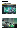
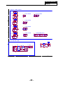
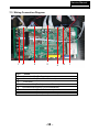
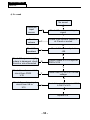
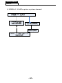
1
SERVICE MANUAL
LED TV
Model No.
MHDV2245-O3-D0
MSD306
Chassis
WARNING
This service information is designed for experienced repair technicians only and is not designed for use by the general public.
It does not contain warnings or cautions to advise non-technical individuals of potential dangers in attempting to service a product.
Products powered by electricity should be serviced or repaired only by experienced professional technicians. Any attempt to
service or repair the product or products dealt with in this service information by anyone else could result in serious injury or death.
Service Manual
Model No.:
Chapter 1: General Information
1-1. Table of Contents
1. General Information...........................................................................1
1-1. Table of Contents
1-2. General Guidelines
1-3. Important Notice
1-4. How to Read this Service Manual
1
3
3
6
2. Specifications.................................................................................... 6
3. Location of Controls and Components........................................... 8
3-1. Board Location
8
3-2. Main Board & AV Board
8
3-3. Power Board
11
3-4. LCD Panel
12
4. Disassemble and Assemble.......................................................... 15
4-1 Remove the Pedestal
15
4-2 Remove the Back Cover
4-3 Remove the Adhesive Tape
15
15
4-4 Remove the Power Module
16
4-5 Remove the Main Board
4-6 Remove the Speaker
4-7 Remove the Remote Control Board
16
17
17
5. Installation Instructions..…....………………...........…………......... 18
5-1 External Equipment Connections
18
5-2 HDMI Connections
21
6. Operation Instructions....…....………………...........…………......... 24
6-1 Front Panel Controls
24
6-2 Back Panel Controls
24
6-3 Universal Remote Control
25
7. Electrical Parts…....………………...........…………......................... 26
7-1. Block Diagram
7-2. Circuit Diagram
26
27
7-3. Wiring Connection Diagram
35
- 01 -
Service Manual
Model No.:
8. Measurements and Adjustments........…………............................ 39
8-1. How to enter into the factory model
42
8-2. How to update software
8-2. How to enter into the hotel model
43
44
9. DVD OPERATION………….............................................................. 45
9-2. DVD Trouble Shooting
49
………….............................................................. 50
10. Trouble-shooting
10-1. Simple Check
50
10-2. Main Board Failure Check
51
10-3. Panel Failure
58
- 02 -
Service Manual
Model No.:
1-2. General Guidelines
When servicing, observe the original lead dress. If a short circuit is found, replace all parts
which have been overheated or damaged by the short circuit.
After servicing, see to it that all the protective devices such as insulation barriers, insulation
papers shields are properly installed.
After servicing, make the following leakage current checks to prevent the customer from
being exposed to shock hazards.
1) Leakage Current Cold Check
2) Leakage Current Hot Check
3) Prevention of Electro Static Discharge (ESD) to Electrostatically Sensitive
1-3. Important Notice
1-3-1. Follow the regulations and warnings
Most important thing is to list up the potential hazard or risk for the service personnel to
open the units and disassemble the units. For example, we need to describe properly
how to avoid the possibility to get electrical shock from the live power supply or charged
electrical parts (even the power is off).
This symbol indicates that high voltage is present inside.It is dangerous to
make any king of contact with any inside part of this product.
This symbol indicates that there are important operating and maintenance
instructions in the literture accompanying the appliance.
1-3-2. Be careful to the electrical shock
To prevent damage which might result in electric shock or fire, do not expose this TV set
to rain or excessive moisture. This TV must not be exposed to dripping or splashing water,
and objects filled with liquid, such as vases, must not be placed on top of or above the TV.
1-3-3. Electro static discharge (ESD)
Some semiconductor (solid state) devices can be damaged easily by static electricity. Such
components commonly are called Electrostatically Sensitive (ES) Devices. The following
techniques should be used to help reduce the incidence of component damage caused by
electros static discharge (ESD).
1-3-4. About lead free solder (PbF)
This product is manufactured using lead-free solder as a part of a movement within the
consumer products industry at large to be environmentally responsible. Lead-free solder
must be used in the servicing and repairing of this product.
1-3-5. Use the genewing parts (specified parts)
Special parts which have purposes of fire retardant (resistors), high-quality sound
(capacitors), low noise (resistors), etc. are used.
When replacing any of components, be sure to use only manufacture's specified parts
shown in the parts list.
Safety Component
● Components identified by
mark have special characteristics important for safety.
- 03 -
Service Manual
Model No.:
1-3-6 Safety Check after Repairment
Confirm that the screws, parts and wiring which were removed in order to service are put
in the original positions, or whether there are the positions which are deteriorated around
the serviced places serviced or not. Check the insulation between the antenna terminal or
external metal and the AC cord plug blades. And be sure the safety of that.
General Servicing Precautions
1. Always unplug the receiver AC power cord from the AC power source before;
a. Removing or reinstalling any component, circuit board module or any other receiver
assembly.
b. Disconnecting or reconnecting any receiver electrical plug or other electrical
connection.
c. Connecting a test substitute in parallel with an electrolytic capacitor in the receiver.
CAUTION: A wrong part substitution or incorrect polarity installation of electrolytic
capacitors may result in an explosion hazard.
2. Test high voltage only by measuring it with an appropriate high voltage meter or other
voltage measuring device (DVM, FETVOM, etc) equipped with a suitable high voltage
probe.
Do not test high voltage by "drawing an arc".
3. Do not spray chemicals on or near this receiver or any of its assemblies.
4. Unless specified otherwise in this service manual, clean electrical contacts only by
applying the following mixture to the contacts with a pipe cleaner, cotton-tipped stick or
comparable non-abrasive applicator; 10% (by volume) Acetone and 90% (by volume)
isopropyl alcohol (90%-99% strength).
CAUTION: This is a flammable mixture.
Unless specified otherwise in this service manual, lubrication of contacts is not required.
Capacitors may result in an explosion hazard.
5. Do not defeat any plug/socket B+ voltage interlocks with which receivers covered by this
service manual might be equipped.
6. Do not apply AC power to this instrument and/or any of its electrical assemblies unless
all solid-state device heat sinks are correctly installed.
7. Always connect the test receiver ground lead to the receiver chassis ground before
connecting the test receiver positive lead.
Always remove the test receiver ground lead last. Capacitors may result in an explosion
hazard.
8. Use with this receiver only the test fixtures specified in this service manual.
CAUTION: Do not connect the test fixture ground strap to any heat sink in this receiver.
9. Remove the antenna terminal on TV and turn on the TV.
10. Insulation resistance between the cord plug terminals and the eternal exposure metal
should be more than Mohm by using the 500V insulation resistance meter.
11. If the insulation resistance is less than M ohm, the inspection repair should be required.
If you have not the 500V insulation resistance meter, use a Tester. External exposure
metal: Antenna terminal Headphone jack
- 04 -
Service Manual
Model No.:
Electrostatically Sensitive (ES) Devices
Some semiconductor (solid-state) devices can be damaged easily by static electricity.
Such components commonly are called Electrostatically Sensitive (ES) Devices.
Examples of typical ES devices are integrated circuits and some field-effect transistors
and semiconductor "chip" components. The following techniques should be used to help
reduce the ncidence of component damage caused by static by static electricity.
1. Immediately before handling any semiconductor component or semiconductorequipped assembly, drain off any electrostatic charge on your body by touching a known
earth ground. Alternatively, obtain and wear a commercially available discharging wrist
strap device, which should be removed to prevent potential shock reasons prior to applying
power to the unit under test.
2. After removing an electrical assembly equipped with ES devices, place the assembly
on a conductive surface such as aluminum foil, to prevent electrostatic charge buildup or
exposure of the assembly.
3. Use only a grounded-tip soldering iron to solder or unsolder ES devices.
4. Use only an anti-static type solder removal device. Some solder removal devices not
classified as "anti-static" can generate electrical charges sufficient to damage ES devices.
5. Do not use freon-propelled chemicals. These can generate electrical charges sufficient
to damage ES devices.
6. Do not remove a replacement ES device from its protective package until immediately
before you are ready to install it.
(Most replacement ES devices are packaged with leads electrically shorted together by
conductive foam, aluminum foil or comparable conductive material).
7. Immediately before removing the protective material from the leads of a replacement
ES device, touch the protective material to the chassis or circuit assembly into which the
device will be installed.
CAUTION: Be sure no power is applied to the chassis or circuit, and observe all other
safety precautions.
8. Minimize bodily motions when handling unpackaged replacement ES devices.
(Otherwise harmless motion such as the brushing together of your clothes fabric or the
lifting of your foot from a carpeted floor can generate static electricity sufficient to damage
an ES device.)
1-3-7. Ordering Spare Parts
Please include the following informations when you order parts. (Particularly the Version
letter)
1. Model number, Serial number and Software Version
The model number and Serial number can be found on the back of each product and the
Software Version can be found at the Spare Parts List.
2. Spare Part No. and Description
You can find them in the Spare Parts List
- 05 -
Service Manual
Model No.:
1-3-8. Photo used in this manual
The illustration and photos used in this Manual may not base on the final design of
products, which may differ from your products in some way.
1-4. How to Read this Service Manual
Using Icons:
Icons are used to attract the attention of the reader to specific information. The meaning of
each icon is described in the table below:
Note:
A “note” provides information that is not indispensable, but may nevertheless be valuable
to the reader, such as tips and tricks.
Caution:
A “caution” is used when there is danger that the reader, through incorrect manipulation,
may damage equipment, loose data, get an unexpected result or has to restart(part of) a
procedure.
Warning:
A “warning” is used when there is danger of personal injury.
Reference:
A “reference” guides the reader to other places in this binder or in this manual, where he/
she will find additional information on a specific topic.
- 06 -
Service Manual
Model No.:
2. Specifications
Model
MHDV2245-O3-D0
Screen Size
21.5inch
Aspect Ratio
16:9
Resolution
Response Time (ms)
5 (GRAY TO
GRAY)
Angel of View
Color Display
No. of Preset Channels 400
OSD Language
English
Color System
PAL/SECAM
Audio System
DK, BG, I, M, L, L'
Audio Output Power
(Built-in) (W)
3W×2
Audio Output Power
(outer) (W)
No
Total Power Input (W)
22.8W
Voltage Range (V)
DC 12V
Power Frequency (Hz) 50~60Hz
Net Weight (KG)
3.9
Gross Weight (KG)
5.2
Net Dimension (MM)
535*165*390
Packaged Dimension
(MM)
610*92*440
- 07 -
Service Manual
Model No.:
3. Location of Controls and Components
3-1 Board Location
B Board
A Board
No.
Description
A Board
Main Board
515C3206M01
B Board
Power Board
514C2415M01
LVDS WIRE
30433920301
3-2 Main Board
- 08 -
Service Manual
Model No.:
3-2-1 Function Description:
Main Board
Process signal which incept from exterior equipment then translate into signal that panel
can display.
3-2-2 Connector definition
Main board connector
Power connectors (J2)
Pin number
1
2
3
4
5
6
J2
Signal name
GND
ADJ
BK ON /OFF
+5V
POWER ON/OFF
+5VSTB
7
+5V
8
+5V
9
GND
10
GND
11
GND
12
13
+12V
+12V
Notes:
J2-Pin 3: Backlight on/off:
The system can turn on or turn off the backlight of TFT LED Panel through the power
supply unit path.
J2-Pin 5: System power on / standby
System board will use this pin to control system power.
J2-Pin 2: Control the luminance of backlight
The system can generate the PWN signal to control the strength of TFT LED Panel’s
backlight through this connector
- 09 -
Service Manual
Model No.:
Keypad andremote connector (J28)
Pin number
1
2
3
4
5
6
Signal name
GND
KEY1
KEY0
7
8
9
10
IR
Description
NC
POWER FOR REMOTE
GND
REMOTE CONTROL
5V
GND
STANDBY
LED_G
LED_R
LAMP GREEN
LAMP RED
Signal name
RSPK+
RSPKLSPKLSPK+
Description
RSPK+
RSPKLSPKLSPK+
Speaker connectorJ26
Pin number
1
2
3
4
- 10 -
Service Manual
Model No.:
3-3. Power Board
3-3-1 Function Description:
Supply power for Main board, Panel.
3-3-2Connectordefinition
7
CN2
Signal name
+12V
+12V
GND
GND
GND
+5V
+5V
8
+5VSTB
9
POWER ON/OFF
+5V
CN1
Pin number
1
2
3
4
Signal name
+12V
+12V
GND
GND
Pin number
1
2
3
4
5
6
10
11
BK ON /OFF
ADJ
GND
12
13
- 11 -
Service Manual
Model No.:
3-4. LED Panel
CLAA215FA04 V4
3-4-1 Function Description: Display the signal.
3-4-2 Connector de finition.
PIN NO.
1
2
3
4
5
6
7
REMARK
RXO0RXO0+
RXO1RXO1+
RXO2RXO2+
GND
FUNCTION
minus signal of odd channel 0(LVDS)
plus signal of odd channel 0(LVDS)
minus signal of odd channel 1(LVDS)
plus signal of odd channel 1(LVDS)
minus signal of odd channel 2(LVDS)
plus signal of odd channel 2(LVDS)
GND
- 12 -
Service Manual
Model No.:
RXOC- minus signal of odd clock channel (LVDS)
8
RXOC+ plus signal of odd clock channel (LVDS)
9
RXO3- minus signal of odd channel 3(LVDS)
10
RXO3+ plus signal of odd channel 3(LVDS)
11
RXE0minus signal of even channel 0(LVDS)
12
RXE0+ plus signal of even channel 0(LVDS)
13
GND
14
GND
RXE1minus signal of even channel 1(LVDS)
15
RXE1+ plus signal of even channel 1(LVDS)
16
GND
17
GND
RXE2minus signal of even channel 2(LVDS)
18
RXE2+ plus signal of even channel 2(LVDS)
19
RXEC- minus signal of even clock channel (LVDS)
20
RXEC+ plus signal of even clock channel (LVDS)
21
RXE3minus signal of even channel 3(LVDS)
22
RXE3+ plus signal of even channel 3(LVDS)
23
GND
24
GND
NC
25
NC
NC
Test pin (Can’t connect to GND)
26
NC
27
NC
VCC
Power supply input voltage(5.0 V)
28
VCC
Power supply input voltage(5.0 V)
29
VCC
Power supply input voltage(5.0 V)
30
1) Keep the NC Pin and don’t connect it to GND or other signals.
2) GND Pin must connect to the ground, don’t let it be a vacant pin.
- 13 -
Service Manual
Model No.:
4. Disassemble and assemble
4-1 Remove the Pedestal
① Lay down the unit so that rear cover
faces upward
① Remove the one screw from the
rear cover indicated with ○
① Then remove the pedestal
4-2Remove the Back Cover
① Remove the these screw indicated on
figure above by ○
①
Then remove the back cover from the
unit.
4-3. Remove the adhesive tape
Remove the adhesive tape indicated on the
figure above
- 15 -
Service Manual
Model No.:
4-4 Remove the power module
Then remove the power module
4-5 Remove the Main board
①
① Remove the two screw indicated on
the figure above by ○
① Then put the terminal bracket to the side
①
① Disconnected the coupler J20①J2①
①J28①CON2①J26①J10 J11
① Remove the Main board
- 16 -
Service Manual
Model No.:
4-7 Remove the speaker
Take out the speaker
4-8 Remove the remote control
Remove the screw, take out the remote control
- 17 -
Service Manual
Model No.:
5. Installation Instructions
5-1 External Equipment Connections
Accessories
Remote Control
User GUIDE
Battery
Antenna Connection
Connect one end of a coaxial cable (not included) to the ANT IN jack on the back of
your TV/DVD combo, then connect the other end of the cable into the antenna or cable
TV wall outlet.
To improve picture quality from an antenna in a poor signal area, install a signal
amplifier.
If you need to split the antenna signal to connect two TVs, install a two-way splitter.
- 18 -
Service Manual
Model No.:
INSTALLATION
- 19 -
Service Manual
Model No.:
Note:
Aerial connections:IEC(female).
Input impendance:75 unbalanced.
PC
STEPS:
Be sure both the TV and computer are
set to Power off.
1.Connect VGA and audio cable.
2.Connect the power cord.
3.Power on the TV, switch to PC mode.
4.Power on the PC.
This sequence is very important.
COMMON INTERFACE (CI)
HDMI1
USB
PRESET MODE
PC AUDIO
SCART
VGA
-6-
- 20 -
RF
Service Manual
Model No.:
5-2 HDMI Connections
When the source device(DVD player or Set Top Box) supports HDM
How To Connect
1. Connect the source device to HDMI port of this TV with an HDMI cable(not supplied
with this product).
2. No separated audio connection is necessary.
How To Use
If the source device supports Auto HDMI function, the output resolution of the source
device will be automatically
set to 1280x720p.
If the source device does not support Auto HDMI, you need to set the output resolution
appropriately.
To get the best picture quality, adjust the output resolution of the source device to
1280x720p.
Select HDMI input source in input source option of Select Main source menu.
When the source device(DVD player or Set Top Box) supports DVI
How To Connect
1. Connect the source device to HDMI port of this TV with a HDMI-to-DVI cable(not
supplied with this product).
2. A separated audio connection is necessary.
3. If the source device has an analog audio output connector, connect the source device
audio output to DVI Audio In port located on the PC port.
How To Use
If the source device supports Auto DVI function, the output resolution of the source device
will be automatically
set to 1280x720p.
If the source device does not support Auto DVI, you need to set the output resolution
appropriately.
To get the best picture quality, adjust the output resolution of the source device to
1280x720p.
Press the INPUT button to select HDMI input source in input source option of Select Main
source menu.
Installation
- 20 -
Service Manual
Model No.:
Cable sample
HDMI Cable
(not supplied with the product)
HDMI to DVI Cable
( not supplied with the product)
Analog Audio Cable
(Stereo to RCA type)
(not supplied with the product)
- 21 -
Service Manual
Model No.:
Power source
TO USE AC POWER SOURCE
Use the AC polarized line cord provided for operation on AC.
Insert the AC cord plug into a standard polarized AC outlet.
NOTES:
■ Never connect the AC line cord plug to other than the specified voltage.
Use the attached power cord only.
■ If the polarized AC cord does not fit into a non-polarized AC outlet,
do not attempt to file or cut the blade. It is the user`s responsibility to have an
electrician replace the obsolete outlet.
■ If you cause a static discharge when touching the unit and the unit fails to function,
simply unplug the unit from the AC outlet and plug it back in. The unit should return to
normal operation.
- 22 -
Service Manual
Model No.:
6. Operation Instructions
Basal information
6-1 Front panel controls
Remote Control
Front control panel
3
1.SOURCE Display the input source menu.
2.MENUDisplay main MENU.
3.CH+/CH-:In TV mode press“CH+”or“CH-”to
Display the input so
1 SOURCE
1
Remote
control sensor.up and down.In MENU
change
the
channel
press
main MENU
2 MENU mode,Display
Indicator LED:
2
In TV mode,press C
3 CH+/CH“CH+”or“CH-”to
select items .In standby mode,
the channel up and
BLUE:POWER ON. RED STAND BY.
In MENU, press CH+
press“CH+”or“CH-”to
turn
on
the
TV.
In standby mode, i
Key board.
3
4 VOL+/VOL4.VOL+/VOL-:Adjust sound level.In MENU
mode, Adjust sound level.
In MENU,adjust the
press“VOL+”or“VOL-”to adjust the item5 that
you
STANDBY
selected.
SOURCE
5. STANDBY
:
Press
MENU this button to turn the unit ON
Rear/Side Sockets
CH+
from STANDBY mode.
Press it again to turn the set
CHback to STANDBY.
AV
R
Y
VOL+
VOL-
1
2
6.2 Back panel
controls
1
2
3
L
STANDBY
4
o change
o select items .
urn on the TV
BUSH|Full HD 1080p LED LCD TV | User Manual | Helpline:0845 604 0105
- 23 -
Pb
Pr
HDMI2
Service Manual
Model No.:
03 Remote control
6-3 Setting Up Your Remote Control
21
/
BUSH|Full HD 1080p LED LCD TV | User Manual | Helpline:0845 604 0105
- 24 -
Service Manual
Model No.:
7. Electrical parts
7-1. Block diagram
2
1
1517
MSD306
- 26 -
Service Manual
Model No.:
7-2. Circuit Diagram
AV1_AR
AV1_AL
05_HDMI
Page 5
Page 3
Page 4
03_AVIN&OUT
HP_SR
HP_SL
HP_SMUTE
SC_ALOUT
SC_AROUT
AV1_AR
AV1_AL
AV1_AL
AV1_AR
04_HD&VGA
Page 10
IRIN
YINO+
PBINO+
PRINO+
SOY
RAIN+
GAIN+
BAIN+
SOG
VSYNC
HSYNC
MUX_AR
MUX_AL
HD1R
HD1L
REAR_AV
DVD_AV
ASEL0
ISP-RXD
ISP-TXD
DVD-ON/OFF
RGB0_RIN+
RGB0_RINRGB0_GIN+
RGB0_GINRGB0_BIN+
RGB0_BINRGB0-SOG
SC1_FS
SC1_FB
AV1-Rin
AV1-Lin
VGA_AR
VGA_AL
SCART_AV
SIDE_AV
SPDIF_O
CVBS_OUT
RX3B0P
RX3B0N
RX3B1P
RX3B1N
RX3B2P
RX3B2N
RX3BCLKP
RX3BCLKN
DDC3BSDA
DDC3BSCL
HOTPLUG3
RX2B0P
RX2B0N
RX2B1P
RX2B1N
RX2B2P
RX2B2N
RX2BCLKP
RX2BCLKN
DDC2BSDA
DDC2BSCL
HOTPLUG2
RX1B0P
RX1B0N
RX1B1P
RX1B1N
RX1B2P
RX1B2N
RX1BCLKP
RX1BCLKN
DDC1BSDA
DDC1BSCL
HOTPLUG1
HDMI_E_CEC
10_MST_POWER
RX3B0P
RX3B0N
RX3B1P
RX3B1N
RX3B2P
RX3B2N
RX3BCLKP
RX3BCLKN
DDC3BSDA
DDC3BSCL
HOTPLUG3
RX2B0P
RX2B0N
RX2B1P
RX2B1N
RX2B2P
RX2B2N
RX2BCLKP
RX2BCLKN
DDC2BSDA
DDC2BSCL
HOTPLUG2
RX1B0P
RX1B0N
RX1B1P
RX1B1N
RX1B2P
RX1B2N
RX1BCLKP
RX1BCLKN
DDC1BSDA
DDC1BSCL
HOTPLUG1
HDMI_E_CEC
RGB0_RIN+
RGB0_RINRGB0_GIN+
RGB0_GINRGB0_BIN+
RGB0_BINRGB0-SOG
SC1_FS
SC1_FB
AV1-Rin
AV1-Lin
VGA_AR
VGA_AL
SCART_AV
SIDE_AV
SPDIF_O
CVBS_OUT
IRIN
YINO+
PBINO+
PRINO+
SOY
RAIN+
GAIN+
BAIN+
SOG
VSYNC
HSYNC
MUX_AR
MUX_AL
HD1R
HD1L
REAR_AV
DVD_AV
ASEL0
ISP-RXD
ISP-TXD
DVD-ON/OFF
Page 8
08_MSD306
MIUA_DQS0
MIUA_DQS0B
MIUA_DQS1
MIUA_DQS1B
MIUA_DQM1
MIUA_DQM0
MIUA_DQ[0:15]
MIUA_MCLK
MIUA_MCLKZ
MIUA_ODT
MIUA_WEZ
MIUA_MCKE
MIUA_BA1
MIUA_BA0
MIUA_A[0:12]
MIUA_BA2
MIUA_RASZ
MIUA_CASZ
ON_USB2
OTG_DM
OTG_DP
OTG_DP1
OTG_DM1
USB_DETEC1
ON_USB1
TSSTART
TSVALID
TSCLK
TS_MDI[7:0]
TS_D[7:3]
TS_CLK
TS_MOSTART
TS_MOVAL
PCM_D[7:0]
PCM_A[14:0]
PCM_IRQA_N
PCM_CE_N
PCM_IOWR_N
PCM_IORD_N
PCM_WE_N
PCM_OE_N
PCM_REG_N
PCM_WAIT_N
PCM_RESET
PCM_CD_N
TS_MDO0
TS_MDO1
TS_MDO2
CLASS_EN
AUOUTL1
AUOUTR1
AMP-Lout
AMP-Rout
HP_DET
POWERON/OFF
BKLON
ADJ-PWM
LCDON
RF_AGC_SELO
#IF_OUT
IF_OUT
IF_AGC
RF_AGC
VIFP
VIFM
TV-SIFP
TV-SIFM
SIF_CTL
T_SDA
T_SCL
MIUA_DQS0
MIUA_DQS0B
MIUA_DQS1
MIUA_DQS1B
MIUA_DQM1
MIUA_DQM0
MIUA_DQ[0:15]
MIUA_MCLK
MIUA_MCLKZ
MIUA_ODT
MIUA_WEZ
MIUA_MCKE
MIUA_BA1
MIUA_BA0
MIUA_A[0:12]
MIUA_BA2
MIUA_RASZ
MIUA_CASZ
ON_USB2
OTG_DM
OTG_DP
OTG_DP1
OTG_DM1
USB_DETEC1
ON_USB1
Page 9
09_MEMORT
Page 7
11_AUDIO
Page 11
TSSTART
TSVALID
TSCLK
TS_MDI[7:0]
TS_D[7:3]
TS_CLK
TS_MOSTART
TS_MOVAL
PCM_D[7:0]
PCM_A[14:0]
PCM_IRQA_N
PCM_CE_N
PCM_IOWR_N
PCM_IORD_N 07_PCMCIA
PCM_WE_N
PCM_OE_N
PCM_REG_N
PCM_WAIT_N
PCM_RESET
PCM_CD_N
TS_MDO0
TS_MDO1
TS_MDO2
CLASS_EN
AUOUTL1
AUOUTR1
AMP-Lout
AMP-Rout
HP_DET
02_SYS_POWER
POWERON/OFF
BKLON
Page 2
ADJ-PWM
LCDON
RF_AGC_SELO
#IF_OUT
IF_OUT
Page 6
IF_AGC
RF_AGC
VIFP
VIFM
TV-SIFP
TV-SIFM
06_TUNER
SIF_CTL
T_SDA
T_SCL
HP_SR
HP_SL
HP_SMUTE
SC_ALOUT
SC_AROUT
HP_SR
HP_SL
HP_SMUTE
SC_ALOUT
SC_AROUT
- 27 -
Service Manual
Model No.:
5
4
3
2
ADJ
OUT
IN
2
3
R269
NC
U11
AMS1117-3.3
D
1
4
MSD306 POWER SUPPLY
U37靠近CA16放置
1.32V
3.29V/380mA
3.3VU
5Vstb
1.31V/1100mA
3.3VU
C124
0.1u
C121
0.1u
C125
C122
0.1u
C123
0.1u
R270
0R
ADJ
OUT
IN
2
3
R271
NC
U12
AMS1117-3.3
5VA
1
4
C126
+
100uF/16V
NC/0.1u
3.29V/150mA
3.3VA
3.3VA
R272
0R
C131
+
C128
NC/0.1u
C130
0.1u
IN
2
3
R273
1k
OUT
U13
AMS1117-ADJ
ADJ
C
1
4
220uF/16V
C127
0.1u
+
C129
100uF/16V
2.54V/230mA
2.5VA
5VA
C135
0.1u
+
C133
0.1u
C134
NC/0.1u
4
C136
R274
1K
C132
NC/0.1u
100uF/16V
2.5VA
OUT
IN
1
2
3
1.8VA
ADJ
R275
U14 470R
AMS1117-ADJ
1.84V/110mA
C137
0.1u
1.8VA
C138
0.1u
230mA(DDR2/PCS)
1.8VA
C139
NC/0.1u
C140
0.1u
C141
0.1u
C142
0.1u
C143
0.1u
C144
0.1u
C145
0.1u
C146
0.1u
C147
0.1u
C148
0.1u
R276
220R
+
C150
C149
0.1u
100uF/16V
3.3VA
B
+1.2V FOR MST CORE
8.12V
+12V
+8V
3
C151
AGND
3
R281
6.8K
FB
5
2K
R282
4.7K
C155
0.1u
C156
0.1u
C157
0.1u
C158
R277
0.1u
2.49K/%1
V8ADJ
0.1uF
R279
470R
GND
GND
GND
+
0.1u
4
SW
15H_2A
1.02A
1.27V
C162
C161
SS
R280
10uF
A
EN
COMP
8
C153
C152
100uF/16V
1.32V
1 C154
15nF
2
C164
15nF
1nF
C159
0.1u
C160
7
6
L80
BS
470uF/16V
100K
R278
VCC
10uF C165
2
C163
5VA
VOUT
4
AdjustTAB
TO-252-4
U15
1
AMS1084-SO263
0.1uF
1.31V
U16
MP1482
VIN
DESIGN:YANXUEWU
CHECKED:
APPRD:
5
4
3
- 28 -
2
+
R299
30K
R292
PVCC
10K
270K
IN4148
R301
220R
220uF/16V
C176
R285
D8
4
GAIN1
R298
NC/10K
R294
GAIN0 NC/10K
AMP
R293
NC/10K
R297
NC/10K
R303
NC/0R
3.3VA
VOLUME
MUTEO
R286
R283
NC/0R
R295
NC/1uF
R289
HP_LINP#
HP_LINN#
+12V
C177
3
6
U17
NC/TPA3110D2
LINP
FAULT
SD
BSPL
PVCCL
PVCCL
AGND
AVCC
GAIN1
GAIN0
PGND
OUTNR
BSNR
BSNL
OUTNL
PGND
OUTPL
GVDD
LINN
PLIMIT
OUTPR
28
26
27
25
24
23
21
22
C166
C178
C179
+12V
C175
NC/1000P
LOUT1-#
LOUT1+#
C172
NC/1000P
NC/FB/1206
ROUTC182
NC/1000P
NC/1uF
C184
NC/1000P
ROUT+
NC/FB/1206
L81
NC/0.22uF
NC/FB/1206
L82
NC/0.22uF
L83
NC/0.22uF
L84
C194
NC/10uF
C207
SD
NC/1uF
+12V
C211
C214
NC/10uF
NC/0R
R345
25
24
23
22
21
C220
C219
NC/1uF
NC/220pF
R347
NC/120K
26
27
28
29
30
L86
ROUTROUT+
NC/FB/1206
C189
C190
NC/1000P
NC/1000P
+12V
NC/FB/1206
19
20
NC/0.22uF
18
C186
17
16
15
+12V
COSC
ROSC
AGND
MUTE
AVCC
V2P5
AGND
SD
VCLAMPR
C197
NC/1uF
C228
NC/1uF
C232
NC/10uF
R288
NC/0R
R296
NC/0R
LOUT+
+ C167
100uF/16V
PVCC
NC/0R AMP1_L+
LOUT-
0.001uF
NC/0R AMP2_R+
NC/0R AMP2_R-
NC/1000P
NC/FB/1206
NC/FB/1206
L89
L88
2
C169
0.1uF
0.1uF
C188
PVCC
NC/0R AMP2_LNC/0R AMP2_L+
R323
R318
R319
SUB_AL+
AMP1_R+
AMP1_R-
SUB_LOUT+
SUB_LOUT-
R331
R335
NC/0R AMP1_L-
R328
NC/0R
R330
NC/0R
R327
MUTEPAM
SUB_AL-
C215
NC/100nF
LOUT1-# R352
NC/0R
LOUT1+# R355
NC/0R
LOUT2-# R359
NC/0R
LOUT2+# R360
NC/0R
C168
MUTETI 1
2
GAIN1
AMP1_L+3
NC/0R
AMP1_L-4
NC/0R
GAIN0
5
7
8
NC/10R
9
10
RINN
BSPR
PVCCR
PVCCR
RINP
NC
PBTL
C193
NC/220nF
+12V
LOUT-
LOUT+
PVCC
J24
+12V
SPEAKER
1
2
3
4
J26
NC/2Pin 2.0MM
C225
NC/1000P
2
1
ROUT-
LOUT-
0R
C224
ROUT+
ROUTLOUTLOUT+
0R
C173
L50
C174
10uF
Q28
3906
FB_56OHM_500MA
4.7K
R306
14
AMP1_R11
NC/0R
AMP1_R+
12
NC/0R
13
L85
NC/FB/1206
C195
NC/220nF
C231
NC/220nF
L90
NC/FB/1206
C170
0.1uF
3.3VA
1R300
R309
C181 NC/1uF
R304
R305 NC/10K NC/10K
C183 NC/1uF
HP_RINN#
R307
HP_RINP#
R311
NC/0R
+12V
C192
NC/10uF
C229
NC/220nF
L91
C234
NC/1000P
0.1uF
L53
NC/FB
3K
Q26
2N3904
MUTEO
L49
3.3VA
3
2
R291
10K
MUTEn
C180
10uF/16V/220uF/16V
Q27
2N3904
-
10K
1
L51
NC
L52
FB_120_OHM_500MA
+
5
R302
+5V
PVCC
LOUT2-#
LOUT2+#
-
CLASS_EN
MUTE Control
CLASS_EN
NC/10K
MUTEPAM
+12V
R317
NC/10K
C196
NC/1uF
GND
C233
NC/FB/1206
NC/1000P
VCLAMPL
31
R316
NC/0R
R320
NC/0R
RINN
RINP
34
NC/PAM8610
U18
35
SD
C201
NC/0.1uF
R333
1
Q30
NC/BT3904
2
AVDD
VREF
VOLUME
REFGND
AGND1
FADE
LINP
BSRP
FADE
R326
NC/10K
HP_RINN#
MUTEPAM
AMP2_RNC/0R
9
8
7
6
5
4
NC/1uF 3
AMP2_R+
NC/0R
C206
R337
AMP2_L+
NC/0R
LINN
NC/1uF
+12V
C230
NC/10uF
36
1
NC/10K
HP_RINP#
HP_RINN#
HP_RINP#
R350
10
BSLP
C227
16
37
BSRN
R310
C187
Q29
NC/10uF
NC/2N3904
NC/0.22uF
HP_LINP#
VOLUME
HP_LINP#
R354
FADE
HP_LINN#
SUB_AL+
AMP2_LNC/0R
R369
NC/1uF
BSLN
R308
0R
0R
R341
C222
2.2uF
R357
10R/0.22uF
R361
HP_LINN#
NC/0.22uF
C237
R367
NC/10uF NC/100
SUB_AL-
15
R312
AUDIO OP
+8V
HP_LINP
C209
2.2uF R338
10R/0.22uF
10R
C239
NC/1u
R366
NC/1.5K
R377
NC/1uF
SUBWOOFER SCH
F=Q/∏RC
38
ROUTN
VCC-OP2
+ C210
100uF/16V
10R HP_RINP
R362
1
NC/4558
U20A
C247
R388
NC/10uF NC/100
LOW PASS
ROUTN
LOUTN
HP_RIN
R336
10R
R344
Gain=R285/R291+1
Q35
3906
VCC-OP2
150R
Gain=R295/R298+1
2
+8V
R384
NC/1.5K
C250
NC/1u
HP_SR
HP_SMUTE
HP_SL
LOUTN
14
100R
Q32
3906
150R
R358
470R
Q36
2N3904
R363
R364
75R
3
Ground in the middle of the L/R
R371
NC/15K
C242
NC/100n
6
7
NC/4558
U20B
HP_SR
HP_SMUTE
HP_SL
13
R313
Q33
2N3904
R339
470R
R346
R349
75R
1
+8V
C235
NC/220n
R365
NC/100K
C238
R368
NC/10uF
NC/15K
R374
NC/100K
R387
NC/15K
5
+8V
NC/100R
39
R314
100K
R370
NC/0R
R372
NC/33K
+8V
C246
NC/220n
R383
NC/100K
C249
R386
NC/10uF
NC/15K
C251
NC/100n
R322
R315
NC/100K
PVCCR
C191
HP_LIN
C185
HP_LIN
1
NC/1uF
R385
NC/0R
R390
NC/100K
5VA
NC/4.7K
PVCCL
200pF
100R
HP_RIN
HP_RINP
HP_LINP
R389
NC/33K
R321
PH_Drive
HP_DET
NC/2200uF/16V
NC/220uF/16V
+5V
NC/FB_56_OHM_4A
L97
C301
NC/0.1uF
40
12
AMP-Rout
R324
R334
SC_AROUT
SC_AROUT
SC_ALOUT
T2
1
2
3
4
5
6
7
8
LOUT+
ROUT+
HP_DET
C204
C205
8
7
6
C300
PGNDR
3
10-2.54MM
2
C236
470uF/16V
C244
0.22uF
NC/1K
VDD
NC/1K
OUTB
C299
PGNDL
AMP-Rout
AMP-Lout
+8V
1K
C212
1uF
SC_ALOUT
GAIN=1K/470R
Q31
2N3904
R343
+8V
1uF
H1
1
2
3
4
10-2.54MM
1
C243
0.22uF
C241
470uF/16V
1
2
R329
R332
OUTA
5
GND
41
thermal
29
11
Location Near
IC Pin.
AMP-Lout
1
330R
R348
1K
Q34 C218
2N3904
R356
330R
T1
1
2
3
4
5
6
7
8
10-2.54MM
LOUT#
ROUT#
GND
MUTE
IN2
BIAS
GND
NC/10UF NC/10UF
GND
C203
C208
R325
100K
100R
C216
1
100K
R353
20
19
18
17
16
15
14
13
12
11
C200
NC/4.7uF
GND
NC/2.2uF
R414
NC/100K
IN1
U25
GND
NC/100K
R375
NC/22K
C202
200pF
R340
200pF
100R
C221
GND/HS
GND/HS
GND/HS
GND/HS
GND/HS
GND/HS
GND/HS
GND/HS
GND/HS
GND/HS
100K
R342
Location Near
IC Pin.
AUOUTR1
AUOUTL1
R351
200pF
IN1
SGND
SVRR
OUT1
PGND
OUT2
VCC
M/SB
IN2
GND/HS
TPA1517
U19
HOLE
GND
1
2
3
4
5
6
7
8
9
10
R381
2R2
HP_RIN C295
1
2
3
4
R416
32
PGNDR
20
C223
1000pF
C226
NC/1000pF
C213
1000pF
C217
NC/1000pF
NC/DF3544
PVCCR
PGNDL
19
AUOUTR1
AUOUTL1
PVCC
HP_LINP#
SVRR
LOUT#
ROUT#
MUTEO R376
HP_RINP# 2K
R380
2R2
+
C298
NC/0.1uF
GND
PVCCL
LOUTP
RX56
R379
2K
SVRR
C248
220uF/16V
GND
NC/2.2uF
ROUTP
33
18
3
ROUTP
LOUTP
17
NC/V800AA
2
3
2
R378
2K
RX57
3
2
+5V
C302
NC/1M
R373
NC/1M
R382
NC/V800AA
3
2
3
2
2
L98
R415
NC/100K
C296
NC/FB_56_OHM_4A
C297
NC/10UFNC/0.1uF
GND GND
HP_LIN
C240
NC/47P
C245
NC/47P
4
8
4
8
D
C
B
A
+
+
+
Service Manual
Model No.:
- 29 -
1
Service Manual
Model No.:
D
13
12
11
10
9
8
7
6
5
4
3
2
1
5
NC/0R +5V
NC/0R
4
5.14V
+12V
L56
C1 +
470uF/16V
10uF
+5V
5VA
0.1u 0.1u
3
LCDON
PANEL POWER
LCDON
ADJ-PWM
BKLON
R14
4.7K
R10 R11
10K 10K
TO INVERTER
BKLON
ADJ-PWM
R18
4.7K
R9
4.7K
R12
10K
1
R8
NC
2
C11
0.01uF
100K
C4 0.1uF
VCCLCDFN
R7
10K
R5
0R
NC/2N3904
Q4
3.3VA
Q2
2N3904
1
+12V
R6
1
R13
4.7K
+5V
+5V
Q3
2N3904
R19
0R
R21
0R
C23
C16
0.1uF
Q1 AO3407
2
3
C10
BL_ON
BL-ADJUST
0.1uF
DESIGN:YANXUEWU
CHECKED:
APPRD:
2
+ C17
100uF/16V
+5V
R15
4.7K
1
2
3
4
5
J25
VCCLCD
NC/INVERTER
1
2
3
4
5
12
1
VER:1.0
TITLE:SYS_POWER
OF
DWG NO.:
2
MODEL: MSDV3205-L2
SHEET:
PART NO.:
1
SHEN ZHEN MTC MULTIMEDIA CO.,LTD
VCCLCDFN
NC
1
C2
C3
0.1uF
1nF
C13 C14 C15
112mA
+5V FB_56_OHM_4A
H:ON
L:OFF
POWERON/OFF#
2N3904
Q5
C22
R23
NC
0.1uF
3
12.21V
C5 +
470uF/16V
C6
C7
C8
C9
0.1uF
1nF
4.7nF
100pF
5.15V
552mA,V315B3_L01
R407
R408
5Vstb
5Vstb
1
100pF C19
1.42A
12.23V
5VSTB#
POWERON/OFF#
5.12V
5Vstb
BL-ADJUST
BL_ON
C20
0.1uF
5Vstb
R20
10k
2N3904
Q6 C24
10n
3
D
C
B
A
- 30 -
C12
0R
L57 FB_56_OHM_4A
5.12V
1.14A
R409
R410
0R
C21 +
470uF/16V
1
100pF C18
MAINPOWER
J2
0.1uF
CON2
1
R22
10k
4
3
2
CON1
DCJACK
3
2
2
3
2
1K
R16
1
2
3
4
CON4-2.0mm
POWERON/OFF
H:ON
L:OFF
C25
10n
3
2
4.7K
R17
J37
DCJACK
1
POWERON/OFF
5
3
2
C
B
A
3
2
Service Manual
Model No.:
D
5
RX1
R25
75R
RX4
SC1_FB
SC1_FS
SC1_FB
SC_ALOUT
AGND
1000pF
C32
SC_AROUT
C31
AGND
1000pF
4
SC_ALOUT
SC_AROUT
AV1-V
L58
FB_11_OHM_500MA
C27
100p
R31
10K
10K
22K
R35
R47
R26
75R
R24
3
C33
C35
100p
C36
C37
100p
47n
1uF
AV1-Rin
AV1-Lin
R50
75R
SCART_AV
AV1-Lin
AV1-Rin
AV Output
75R
Q9 3906
2N3904Q8
1
47nF Location near MST.IC
33R C26
R:10ohm,C:1uF 47nF Location near MST.IC
R34
10K
R36
10K
+8V
R48
330R
R49
1uF
Keep AGND trace with signal
R:10ohm,C:1uF
Keep spacing for L/R
AV1-L
RGB0-SOG
RGB0_GIN+
RGB0_BIN+
C45
1
R52
75R
AGND
J5
1
4
5
2
3
6
PC Audio Input
100pF
SCART_AV
VOUT
C47
C55
R57
R58
10K
10K
2
C30
C28
NC/0.1uF
NC/0.1uF
6
5
4
3
2
1
SPDIF_O
1
2
3
4
5
6
R28
NC/1K
1
NC/1uF
R27
NC/150R
C29
R32
NC/150R
5V-IF
NC/3906
Q7
VOUT
10K
10K
SC_AROUT
SC_ALOUT
R29
NC/220R
VGA_ARIR53
VGA_ALI R54
VGA_AL
VGA_AR
APPRD:
CHECKED:
DESIGN:YANXUEWU
1
2
1
2
1
NC/OUTPUT
J4
SPDIFOUT
VER:1.0
TITLE:AVIN&OUT
12
DWG NO.:
OF
MODEL: MSDV3205-L2
3
1
SHEN ZHEN MTC MULTIMEDIA CO.,LTD
SHEET:
PART NO.:
C34
NC/33pF
L59
SPDIFOUT
NC/FB_11_OHM_500MA
C:1uF Location near MST.IC
Keep AGND trace with signal
Keep spacing for L/R
Keep trace width(12mil+)
C51
VGA_ALI
VGA_AL
VGA_ARI1uF VGA_AR
C52 1uF
NC/AV-JACK-3/AVOUT
J32
SPDIF_O
SPDIF Output
(AV+SPDIF) Output
C54
100pF 100pF
NC/V800AA RX3
SCART
P1
NC/V800AA
R33
1n
10K
R30
47n RGB0_GIN+
SC1_FSO
SC1_FSO
0-2v: TV Mode
5-8v: 16:9 AV
9.5-12v: 4:3 AV
0R C38
47n RGB0_BIN+
2.2K NC/V800AA
AV1-R
33R C39
RGB0_RIN+
RGB0_BINRGB0_GIN-
CVBS_OUT
RGB0_RIN-
4.7uF/1206
R51
10K
J34
2
3
AV1-V
VOUT
Pr
Y
Pb
AV1-L
SC_ALOUT
AV1-R
SC_AROUT
R:10ohm,C:1uF 47nF Location near MST.IC
R37
33R C40
RGB0-SOG
R38
47n RGB0_BIN-
R39
47n RGB0_GIN-
Y
68R C42
Pb
SC_AROUT
SC_ALOUT
68R C43
AV1-R
AV1-L
R44
47n RGB0_RIN+
R45
33R C41
RX7
R40
RX6
Pr
RX5
Pb
Y
47n RGB0_RIN-
1
2
D
C
B
A
- 31 -
Pr
68R C44
AV1_AR
AV1_AL
CVBS_OUT
R46
AV1_AL
AV1_AR
47nF Location near MST.IC
AGND trace with signal
spacing for L/R
trace width(12mil+)
SIDE_AV
2
7
AV1-V
C48 1uF
SIDE CVBS Input
NC/V800AA NC/V800AA NC/V800AA
HP_SR
HP_SL
HP_SMUTE
R56
10K
C53 1uF
SIDE_AV
R:10ohm,C:1uF
Keep
Keep
Keep
47n
1
3
4
5
8
7
SC1_FB
VOUT
SC1_FSO
10K
10K
HP_SR
HP_SL
HP_SMUTE
R55
R59
R60
10K
C56
1
2
3
4
RX8
21
20
19
18
17
16
15
14
13
12
11
10
9
8
7
6
5
4
3
2
1
24
23
22
21
20
19
18
17
16
15
14
13
12
11
10
9
8
7
6
5
4
3
2
1
C49
100pF
C50
100pF
L60
FB_11_OHM_500MA
47R
1
SIDE_AVIN
SIDE_AULIN
8
2
3
NC/SCART
24
23
22
21
20
19
18
17
16
15
14
13
12
11
10
9
8
7
6
5
4
3
2
1
SIDE_AURIN
R61
J7
2
3
4
6
NC/V800AA
SCART_24
J27
J6
NC/Headphoto
1
2
3
4
1
2
3
4
SIDE_AVIN
SIDE_AULIN
R62
75R
2
3
4
5
7
NC/V800AA
6
AV-JACK-3/AV
3
8
3
2
R43
RX2
SIDE_AURIN
8
5
6
7
8
5
6
7
C57
7
R42
75R
24
1
2
3
4
8
7
R41
75R
25
25
1
2
3
4
100pF
AV-JACK-3/AV
4
8
75R
26
25
J33
NC/Side_AV
RX9
C
B
A
5
NC/V800AA
26
Service Manual
Model No.:
D
4
1
HD1LIN
HD1RIN
C61
100pf
1
C62
10K
10K
R63
R64
10K
R65
10K
R67
100pF
J35
NC/V800AARX17
NC/V800AARX17
NC/V800AARX18
NC/V800AARX18
3
C58
1uF
4
3
2
1
C59 1uF
J10
CON4
4
3
2
1
CON7
J11
1
2
3
4
5
6
7
HD1L
HD1R
1
2
3
4
5
6
7
VSYNC
HSYNC
BAIN+
GAIN+
10uF
YIN
PBIN
PRIN
0.1uF
ASEL0
L61
2
L62 FB_11_OHM_500MA
L63 FB_11_OHM_500MA
2
APPRD:
75R 75R
100K
100K
100K
100K
100K
100K
100K
100K
YINO
PBINO
PRINO
R66
R68
R69
R70
33R
33R
33R
0R
C60
C63
C64
C65
1
47nF
47nF
47nF
1nF
YINO+
PBINO+
PRINO+
SOY
R & C Location near MST.IC
YINO
PBINO
PRINO
75R
R74
R81
47R
47R
C73
C69
+8V
YINO+
PBINO+
PRINO+
SOY
REAR_AV
MUX_AL
MUX_AR
DVD_AV
47n REAR_AV
47n DVD_AV
L67
FB_11_OHM_500MA
C80
VCC1
10uF
MUX_AL
MUX_AR
C79
1u
C82
1u
C85
0.1uF
13
3
VER:1.0
TITLE:HD&VGA
12
DWG NO.:
OF
MODEL: MSDV3205-L2
4
1
SHEN ZHEN MTC MULTIMEDIA CO.,LTD
SHEET:
PART NO.:
4052SW
U1
R76
R:10ohm C:47n Location near MST.IC
L64
AGND
100pF
R75
C70
FB_11_OHM_500MA
L66
7
6
10
9
1
5
2
4
12
14
15
11
100pF
C76
FB_11_OHM_500MA
DVD-ON/OFF
IRIN
DVD_AVIN
CHECKED:
DESIGN:YANXUEWU
Q10
2N3904
R92
R93
R85
R86
R87
R88
R89
R91
DVD_AR
DVD_AL
75R
R71 R72 R73
FB_11_OHM_500MA
AV1
1uF
NC
NC
1uF
R77
R78
C74
DVD-ON/OFF
IRIN
C75
+5V
100R
10R
VCC1
AV1_AR
AV1_AR
DVD_AR
R99
R103
1
4.7K
AV1_AL
DVD_AL
4.7K
AV1_AL
VCC1
R82
R83
100R
100R
FB_56_OHM_4A
L65
33pF C68
R79
R80
33pF C67
DVD_AVIN
ASEL0
RX10
RX11
RX12
NC/V800AA
NC/V800AA
NC/V800AA
5
1
2
3
4
5
6
GAIN+
RAIN+
SOG
33pF C66
AV1/YPbPr/DVD INPUT
J8
HD1LIN
HD1RIN
1
2
3
4
5
6
VSYNC
HSYNC
C86
RAIN+
BAIN+
C87
SOG
C83
C88
RX13
1
2
J9
YIN
PBIN
PRIN
47nF
47nF
47nF
1nF
NC/V800AA
1
2
PBIN
YIN
2
3
4
5
6
100R
100R
33R
33R
33R
0R
C71
9
3
4
2
3
4
5
6
GSCL
GSDA
R94
R95
R96
R97
R98
R102
3
C72
9
3
4
NC/V800AARX20
NC/V800AARX20
8
PRIN
AV1
NC/V800AARX19
NC/V800AARX19
8
5
6
7
L70
L71
FB_11_OHM_500MA
FB_11_OHM_500MA
AV-JACK-3/YPbPr
8
AV-JACK-3/YPbPr
7
8
4
D
C
B
A
- 32 -
7
FB_11_OHM_500MA
L69
RX15
5
6
7
ISP-TXD
RX14
NC/V800AA
NC/Audio
IVS
IHS
GBLU
GGRN
GRED
ISP-TXD
GSCL
75R R106
7
75R R104
VGA INPUT
15
5
10
14
4
9
13
3
8
12
2
7
11
1
6
0R
0R
NC/V800AA
75R
16
8
3
2
J12
R107
PC_DB15HD_MIDDLE
GSDA
ISP-RXD R108
75R R105
8
7
10K R101
C
B
A
ISP-RXD
5
NC/V800AARX16
NC/V800AARX16
8
10K R100
16
17
D
39
40
41
42
5
J13
HDMI19/Rear
1 DATA2+
2 DATA2 SHIELD
3 DATA24 DATA1+
5 DATA1 SHIELD
6 DAT1A7 DATA0+
8 DATA0 SHIELD
9 DATA010 CLK+
11 CLK SHIELD
12 CLK13 CEC
14 NC
15 SCL
16 SDA
17 DDC/CEC GND
GND 18 +5V POWER
GND 19 HOT PLUG
GND
GND
HDMI2/5V
HOTPLUG_2
HDMI_CEC
1
2
3
4
5
6
7
8
9
10
11
12
13
14
15
16
17
18
19
HDMI_CEC
HDMI3/5V
HOTPLUG_3
RX2B2P
RX2B2N
RX2B1P
RX2B1N
RX2B0P
RX2B0N
RX2BCLKP
RX2BCLKN
DDC2BSCL
DDC2BSDA
RX3B2P
RX3B2N
RX3B1P
RX3B1N
RX3B0P
RX3B0N
RX3BCLKP
RX3BCLKN
DDC3BSCL
DDC3BSDA
HOTPLUG2
4
R117
R110
10K
HOTPLUG_2
RX2BCLKN
HOTPLUG2
4.7K
HDMI2/5V
R109
1K
Q11
3904
5VA
D2
HDMI2/5V
2
1
3
BAV70L
R113
R111
22K
22K
C92
0.1u
3
RX2B2P
RX2B2N
RX2B1P
RX2B1N
RX2B0P
RX2B0N
RX2BCLKP
RX2BCLKN
DDC2BSCL
DDC2BSDA
HOTPLUG3
HDMI3/5V
RX2B2P
RX2B2N
RX2B1P
RX2B1N
RX2B0P
RX2B0N
RX2BCLKP
RX2BCLKN
DDC2BSCL
DDC2BSDA
HOTPLUG3
J15
R114
10K
2
4
6
8
10
12
14
16
18
20
R118
2
4
6
8
10
12
14
16
18
20
4.7K
1
3
5
7
9
11
13
15
17
19
DIP-20(2*10)
R125
R123
10K
HDMI1/5V
HOTPLUG1
2
Q12
3904
HDMI3/5V
HOTPLUG_3
HDMI1/5V
R115
1K
Q13
3904
RX1B2P
20
21
22
23
24
25
26
27
28
29
30
31
32
33
34
35
36
37
38
HDMI_CEC
HOTPLUG1
RX1B2N
43
44
45
46
47
1 DATA2+
NC 2 DATA2 SHIELD
NC
3 DATA2NC
4 DATA1+
5 DATA1 SHIELD
GND
6 DAT1AGND
7 DATA0+
8 DATA0 SHIELD
9 DATA010 CLK+
11 CLK SHIELD
12 CLK13 CEC
14 NC
15 SCL
16 SDA
17 DDC/CEC GND
18 +5V POWER
19 HOT PLUG
4
R121
1K
HDMI3/5V
5VA
2
3.3VU
HDMI1/5V
D4
D3
3
BAV70L
R112
R116
C91
0.1u
22K
22K
HDMI_E_CEC
R122
22K
22K
0.1u
C93
R124
NC/100R
R119
NC/47K
R120
3
BAV70L
APPRD:
CHECKED:
DESIGN:YANXUEWU
1
2
HDMI_CEC
5VA
1
1
1
5
OF
12
RX3B2P
RX3B2N
RX3B1P
RX3B1N
RX3B0P
RX3B0N
RX3BCLKP
RX3BCLKN
DDC3BSDA
DDC3BSCL
RX1B2P
RX1B2N
RX1B1P
RX1B1N
RX1B0P
RX1B0N
RX1BCLKP
RX1BCLKN
DDC1BSCL
DDC1BSDA
TITLE:HDMI
DWG NO.:
VER:1.0
SHEN ZHEN MTC MULTIMEDIA CO.,LTD
SHEET:
PART NO.:
MODEL: MSDV3205-L2
RX1B2P
RX1B2N
RX1B1P
RX1B1N
RX1B0P
RX1B0N
RX1BCLKP
RX1BCLKN
DDC1BSCL
DDC1BSDA
RX3B2P
RX3B2N
RX3B1P
RX3B1N
RX3B0P
RX3B0N
RX3BCLKP
RX3BCLKN
DDC3BSDA
DDC3BSCL
RX36
4.7K
NC/V80010
RX49
NC/V80010
21
RX3B0P
RX35
NC/V80010
J36
RX1B0P
NC/V80010
RX1B1P
RX3B2P
HDMI_E_CEC
RX3B0N
RX34
RX1B0N
NC/V80010
RX47
NC/V80010
RX48
RX33
RX1B1N
J14
RX3B1P
NC/V80010
RX46
RX3B2N
RX3B1P
RX3B1N
RX32
NC/V80010
22
23
20
RX3B2P
NC/V80010
NC/V800AA
RX41
RX31
RX40
NC/V80010
RX39
RX30
NC/V800AA
NC/V80010
NC/V800AA
RX29
NC/V80010
RX3B1N
RX3B0P
HDMI
RX45
NC/V80010
RX51
DATA2+
21
DATA2 SHIELD
DATA2DATA1+
DATA1 SHIELD
DAT1ADATA0+
DATA0 SHIELD
DATA0CLK+
CLK SHIELD
CLKCEC
22
NC
23
SCL
SDA
DDC/CEC GND
+5V POWER
HOT PLUG 20
2
RX3B2N
RX28
RX50
RX3B0N
RX3BCLKP
1
2
3
4
5
6
7
8
9
10
11
12
13
14
15
16
17
18
19
1
3
5
7
9
11
13
15
17
19
RX3BCLKP
NC/V80010
RX1BCLKP
RX27
NC/V800AA
RX3BCLKN
DDC3BSCL
DDC3BSDA
RX3BCLKN
NC/V80010
RX1BCLKN
RX26
RX44
HDMI_CEC
HDMI3/5V
HOTPLUG_3
RX2B0P
NC/V80010
NC/V80010
21
1
2
3
4
5
6
7
8
9
10
11
12
13
14
15
16
17
18
19
3
RX2B0N
RX25
RX43
21
DATA2+
DATA2 SHIELD
DATA2DATA1+
DATA1 SHIELD
DAT1ADATA0+
DATA0 SHIELD
DATA0CLK+
CLK SHIELD
CLK22
CEC
NC
SCL
SDA
DDC/CEC GND
+5V POWER
HOT PLUG
RX2B1P
NC/V80010
NC/V80010
D
C
B
A
- 33 -
RX2B1N
RX24
RX42
20
HDMI/Side
RX2B2P
NC/V80010
RX38
RX23
RX37
NC/V80010
NC/V800AA
RX22
NC/V800AA
NC/V80010
NC/V80010
22
20
RX2B2N
RX21
NC/V800AA
C
B
A
5
RX2BCLKP
NC/V80010
5
4
3
2
PAL /DVB-T SYSTEM
U2
Q14
100R
IF_AGC_T
R417
NC/0R
3 3906 2
Q15
RF_AGC_T
IF_AGC
IF_AGC
C94
Body
Body
B1
NC
1
0.1uF
5V-IF
VOUT
2
AdjustTAB
4
VIN
C100
3.3VA
R127
10K
TO-252-4
1
VTVCC1
L72
FB_56OHM_4A
C101
C102
C96
U3
AMS1084-SO252
0.1uF
C97
C98
C99
C95
220uF/16V
220uF/16V
0.1uF 0.015uF
330pF
0.001uF
R128
10K
33pF 33pF
R129
3
SDA
SCL
RF_AGC
2
1
R126
100K
IF_OUT
#IF_OUT
T_SDA
T_SCL
C103C104
14
13
AS
VTU_TP
B2
5
4
3
8
7
6
5.04V
449mA
5V-IF
3
IF_OUT
#IF_OUT
T_SDA
T_SCL
VTVCC1
T_SDA
T_SCL
RF_AGC_T
VTVCC1
Q16
N3904
1
R131
10K
RF_AGC_SELO
R130
1.5K
RF_AGC_SELO
510R
2
12
11
10
9
Body
Body
AIF
DF1
DF2
IF_AGC
0.1uF
15
16
POWER FOR ATV TUNER
RF_AGC
+8V
TDTC-G0X1D
IF_TV
#IF_OUT
IF_OUT
IF_AGC_T
RF_AGC
D
LS1
3.3VCC_T
NC/120ohm_FBCS1
NC/0.1uF
Vdd_A1.6V
RS2
1.8VCC
CS6
SIFP_OUT
NC/10nF
CS21
SIFP_OUTNC/10nF
NC/391
CS2
LS2
NC/2.2uF
RS4
NC/120ohm_FB
CS4
NC/0.1uF
Q17
NC/1K
RF_AGC_T
NC/1000pF
LS5
CS34 NC/10nF VIFN_OUT
LS3
Pin 1 RS5
Pin 1 RS7
NC/391
CS3
301RF V8
DNP
0
LS4
301RF V7 MM
0
DNP
CS5
XTAL_N
25
VAGC1
IF_OUTP
26
27
28
VBATT_A2
29
TF_3
30
31
VDD_DNX1
TF_2
SDA
SCL
15
14
VBATT_A1
VREG_A_OUT1
13
9
GND_DIG
OUT
IN
1
2
3
NC/100R
#IF_OUT
Vdd_A1.6V_D
LS10
RS9
LS12
18
CLOSE IC
CS20
NC/120ohm_FB
NC/47R
NC/120ohm_FB
LS13
CS19
3.3VCC_T
Vdd_A1.6V_D
NC/120ohm_FB
NC/0.1uF
17
NC/2.2uF
F1
3.3VCC_T
3.3VCC_T
NC
NC/0R
Vdd_IO
NC/120R
R196
NC/4700pF
IF_OUT
LS16
CS31
NC/220nH
NC/39pF
22
20
19
VREG_D_OUT
C263
21
VBATT_A4
VREG_D_IN
LS15
RS16
NC/391
RS14
NC/4K7
RS15
NC/4K7
SSDA
3.3VCC_T
SSCL
NC/120ohm_FB
CS22
ADJ
T_SDA
T_SCL
RS17
NC/391
CS23 CS24
NC/18nF
NC/18pF
NC/0.1uF
Y2
RS23
NC/0R 2
3.3VCC_T
1
NC/24MHZ
+
CS25
NC/100uF/16V
CS29
NC/100nF
CS26
NC/2.2uF
NC
Vdd_A1.6V_D
Important:
Analog GND and digital GND is still separate,
but through Paddle GND connecting them,
+8V
VIF_8V
J3
J29
J30
J31
1
CS28
NC/100uF/16V
CS27
1
CS36
NC/100nF
CS32
NC/100nF
NC
VDD_REF_SX
NC/MXL301RF
NC/120ohm_FB
5VA
CS39
23
1
3
LS14
24
NC
VIFNS
NC/4700pF
VIFPS
NC/4700pF
1
2
4
IN
1
RS13
3.3VCC_T
CS8
IF_OUTN
VDD_IO
VBATT_A5
8
Put on digital GND plane
RS10
NC/0R
Close Silicon Tuner
NC/100R
16
7
RS25
VREG_A_OUT2
AS
4
OUT
US1
NC/AMS1117-3.3
1.8VCC
NC/100uF/16V
33
VAGC2
6
RS18
5VA
32
VBATT_A3
5
NC/0.1uF
Vdd_A1.6V_D
RS12
ADJ
US2
NC/AMS1117-1.8
TF_1
IDAC
4
CS17
NC/100R
C
PADDLE
3
NC/120ohm_FB
GND_XTAL
IF_AGC
LNA_IN
CLK_OUT
NC/220nH
LS11
VDD_DNX2
2
XTAL_P
3.3VCC_T
LS7
NC/330nH
LS9
CS18
NC/82p
RS8
NC/1M CS16
NC/180p
1
12
CS12
NC/1nF
U4
NC/0.1uF
LS8
NC/12nH
11
CS9
NC
10
Vdd_RF_VCO_LO_3V
RS7
CS10
NC/56p
3
3
7
8
9
10
4
1
2
6
5
CS7
Vdd_A1.6V
DS1
NC/BAV99
CS13
CS14
NC/39p NC/27pF
F Conn
R194
NC/4700pF
CS35 NC/10nF VIFP_OUT
LS6
NC/120ohm_FB
1
2
NC/1M
75 ohm Line
JS1
RF Input
Port
LNA GND
NC/3.6nH
RS3
NC/10K
C262
NC/120nH
RS24
NC/0R
CS30
NC/10nF
RS6
RS6
NC/33nH
NC/0.1uF
1.8VCC
3.3VCC_T
3.3VCC_TM
5V-IF
R132
NC/100R
C105
R133
NC/4.7K
C107
NC/10n
L73
NC/0.82uH
R134
NC/680R
R135
NC/6.8K
R136
NC/1k
C108
R137
NC/39R
L74
0R
C110
NC/15nF
U5
SIFP_OUT
NC/47nF
Q18
NC/2SC2216
1
R139
NC/56R
1 IN
SAW OUT2
D5
R138
NC/BA277
NC/2.2K
SIFP_OUT- 2
ING
5
C109
4
C111
TV-SIFP
NC/0.1uF
TV-SIFM
NC/0.1uF
3.3VA
OUT1
3
2
IF_TV
3
B
GND
C106
nc/15nF
NC/10uF
TV-SIFP
TV-SIFM
NC/D9650N
R140
NC/1.5K
R141
NC/22R
R143
NC/10K
3
R142 5V-IF
NC/2.2K
R144
NC/100K
1
R145
2
NC/MM3904
Q19
0R
SIF_CTL
SIF_CTL
C112
NC/15nF
R418
NC/0R
U6
D8602F5/K6966M/D3953N
C113
47nF
VIFP_OUT 1 IN
SAW OUT2
5
C114
4
L75
2.2uH
C115
VIFM
VIFM
0.1uF
NC
2
OUT1
VIFP
VIFP
0.1uF
3
ING
GND
L92
R146
NC/390R
R147
VIFN_OUT
0R
R419
NC/0R
A
5
4
3
- 34 -
2
Service Manual
Model No.:
5
5VA
R149
1K
1
D9
BAV99L
3
R150
100R
PCM_CD_N
R153
1k
4
C117
0.1u
C257
10uF
NC/CON4
3
1
2
3
45
4
3
2
1
J17
USB1IN
J1
5VUSB1
+
2
ON_USB1
ON_USB2
5VA
+
NC/CON4
100uF/16V
C118
5VUSB1
OTG_DM
OTG_DP
+5V
3.3VA
3.3VA
ON_USB1
ON_USB2
1
2
3
45
5V card
L93
FB_11_OHM_500MA
5VUSB2
2
2
1
2
3
4
U7
1
OTG_DM1
OTG_DP1
5VUSB2
5VUSB1
OTG_DM1
22R OTG_DP1
22R
USB_DETEC1
2
R159
R161
VCC-PCMCIA
10K
2
8 6 4 2
7 5 3 1
TITLE:PCMCIA
10K
DWG NO.:
1
R174
R401
R394
NC/1K
DM
DP
1
8
7
6
5
MODEL: MSDV3205-L2
3.3VA
PS6231/PS6232
3.3VA
USB Power
J19
R411
1 10K
R169
1 10K
NC/USB2IN
4
3
2
1
J18
PWR CTRL
NC/NSMD050
OTG_DM
22R OTG_DP
22R
F1
C256
5VUSB2
USB_DETEC1
+5V
NC/NSMD050
USB_DETEC1
F2
R158
R160
USB Interface
+5V
NC/100uF/16V
RX54
CARD DETECT
R148
1K
PCM_CD1_N
2
TSVALID
TSCLK
PCM_D[7:0]
PCM_A[14:0]
PCM_CD_N
PCM_RESET
PCM_WAIT_N
PCM_REG_N
PCM_OE_N
PCM_WE_N
PCM_IORD_N
PCM_IOWR_N
PCM_CE_N
PCM_IRQA_N
RX55
PART NO.:
D
C
B
A
- 35 -
PCM_CD2_N
VCC-PCMCIA
PCM_D3
PCM_D4
PCM_D5
PCM_D6
PCM_D7
PCM_CE_N
PCM_A10
PCM_OE_N
PCM_A11
PCM_A9
PCM_A8
PCM_A13
PCM_A14
PCM_WE_N
PCM_IRQA_N
TSVALID
TSCLK
PCM_A12
PCM_A7
PCM_A6
PCM_A5
PCM_A4
PCM_A3
PCM_A2
PCM_A1
PCM_A0
PCM_D0
PCM_D1
PCM_D2
TS_D[7:3]
PCM_D[7:0]
PCM_A[14:0]
PCM_CD_N
PCM_RESET
PCM_WAIT_N
PCM_REG_N
PCM_OE_N
PCM_WE_N
PCM_IORD_N
PCM_IOWR_N
PCM_CE_N
PCM_IRQA_N
RX52
J16
PCMCIA_CNT
1
2
3
4
5
6
7
8
9
10
11
12
13
14
15
16
17
18
19
20
21
22
23
24
25
26
27
28
29
30
31
32
33
34
TS_D[7:3]
TS_CLK
NC/V800AA
VCC-PCMCIA
GND
GND
CD1#
D3
MDO3
D4
MDO4
D5
MDO5
D6
MDO6
D7
MDO7
CE1#
CE2#
A10
VS1#
OE#
IORD#
A11
IOWR#
A9
MISTRT
A8
MDI0
A13
MDI1
A14
MDI2
WE#
MDI3
READY
VCC
VCC
VPP2
VPP1
MDI4
MIVAL
MDI5
MICLK
MDI6
A12
MDI7
A7
MOCLK
A6
RESET
A5
WAIT#
A4
INPACK
A3
REG#
A2
MOVAL
A1
MOSTART
A0
MDO0
D0
MDO1
D1
MDO2
D2
CD2#
WP
GND
GND
TS_D3
TS_D4
TS_D5
TS_D6
TS_D7
TS_CLK
RX53
PCM_CD1_N
TS_MDO3
TS_MDO4
TS_MDO5
TS_MDO6
TS_MDO7
35
36
37
38
39
40
41
42
43
44
45
46
47
48
49
50
51
52
53
54
55
56
57
58
59
60
61
62
63
64
65
66
67
68
TS_MDO0
TS_MDO1
TS_MDO2
TS_MOSTART
TS_MOVAL
22R
DESIGN:YANXUEWU
NC/V800AA
PCM_IORD_N
PCM_IOWR_N
TSSTART
TS_MDI0
TS_MDI1
TS_MDI2
TS_MDI3
TS_MDI4
TS_MDI5
TS_MDI6
TS_MDI7
TS_MOCLK
PCM_RESET
PCM_WAIT_N
22R
RP1
TS_MDI[7:0]
PCM_REG_N
TS_MOVAL
TS_MOSTART
TS_MDO0
TS_MDO1
TS_MDO2
PCM_CD2_N
R175
TS_MDO0
TS_MDO1
TS_MDO2
TS_MDO3
R173
TS_MDO4 22RX4
TS_MDO5
TS_MDO6
TS_MDO7
TS_MOCLK
TS_MOSTART
TS_MOVAL
NC/V800AA
PCMCIA Connector
TSSTART
TS_MDI[7:0]
TS_MDO[7:0]
6
D
C
B
A
6
CHECKED:
NC/V800AA
9
R166
R168 NC/51K
NC/100K
GND
GND
GND
GND
72
71
70
69
Service Manual
Model No.:
D
MSD306
RX2B0N
RX2B0P
RX2B1N
RX2B1P
RX2B2N
RX2B2P
RX2BCLKN
RX2BCLKP
DDC2BSCL
DDC2BSDA
HOTPLUG2
RX3B0N
RX3B0P
RX3B1N
RX3B1P
RX3B2N
RX3B2P
RX3BCLKN
RX3BCLKP
DDC3BSCL
DDC3BSDA
HOTPLUG3
RX2B0N
RX2B0P
RX2B1N
RX2B1P
RX2B2N
RX2B2P
RX2BCLKN
RX2BCLKP
DDC2BSCL
DDC2BSDA
HOTPLUG2
Y7
W8
Y8
W9
Y9
AA9
W7
AA7
U9
V9
AA6
B2
B1
C2
C1
D2
D1
A2
C3
J5
K4
K5
E2
F3
F2
G3
G2
G1
E3
E1
H5
H6
J6
L3
K1
M3
L2
N3
M2
L1
M5
N4
5
HDMI
MSD306
AUDIO
PAD_LINEIN_L0
PAD_LINEIN_R0
PAD_LINEIN_L1
PAD_LINEIN_R1
PAD_LINEIN_L2
PAD_LINEIN_R2
PAD_LINEIN_L5
PAD_LINEIN_R5
PAD_LINEOUT_L0
PAD_LINEOUT_R0
PAD_LINEOUT_L3
PAD_LINEOUT_R3
PAD_EARPHONE_OUTL
PAD_EARPHONE_OUTR
I2S
PAD_VRP
PAD_VAG
AVSS_VRM_ADC_DAC
PAD_I2S_OUT_MCK
PAD_I2S_OUT_SD
PAD_I2S_OUT_WS
PAD_I2S_OUT_BCK
N6
R6
V12
U12
U10
V10
N5
L4
R5
T6
P6
P5
T4
T5
AMP-Lout
AMP-Rout
AUOUTL1
AUOUTR1
AV1-Lin
AV1-Rin
HD1L
HD1R
VGA_AL
VGA_AR
MUX_AL
MUX_AR
CVBS_OUT
C259
1u
C260
1u
4
PCM_CE_N
PCM_WE_N
PCM_CD_N
PCM_WAIT_N
PCM_IOWR_N
PCM_REG_N
PCM_A12
PCM_RESET
R192
R193
R195
CI_IRQA_N
CI_OE_N
CI_IORD_N
R190
R191
R186
PCM_CE_N 22R
PCM_WE_N 22R
PCM_CD_N
PCM_WAIT_N
22R
PCM_IOWR_N
22R
PCM_REG_N
22R
CI_A10
CI_OE_N
CI_IORD_N
CI_A1
G21
G20
G19
RP7
CI_A13
CI_A8
CI_A14
CI_IRQA_N
LCDON
EEP_WP
BKLON
RP8
PCM_RESET
LCDON
L77
DVD-ON/OFF
ASEL0
FB220/100mA
SPDIF_O
BKLON
PCM_A10
PCM_OE_N
PCM_IORD_N
PCM_A11
22RX4
PCM_A13
22RX4
PCM_A8
PCM_A14
PCM_IRQA_N
RXE1RXE1+
RXE2RXE2+
RXECRXEC+
RXE3RXE3+
RXO0RXO0+
RXO1RXO1+
RXO2RXO2+
RXOCRXOC+
RXO3RXO3+
RXE0RXE0+
PCM_OE_N
PCM_IORD_N
PCM_IRQA_N
靠近MSD306放置
RP9
RP10
RP11
RP12
W21
U16
V17
T17
V21
T15
M21
P16
N20
MSD306
2 4 6 8
1 3 5 7
MVERF
R230
10k
1.8VA
MVREF
PAD_IO[36](A_WEZ)
PAD_IO[9](A_RASZ)
PAD_IO[7](A_CASZ)
PAD_IO[39](A_BA0)
PAD_IO[38](A_BA1)
PAD_IO[40](A_BA2)
PAD_IO[11](A_ODT)
PAD_IO[12](A_MCLK)
PAD_IO[10](A_MCLKZ)
PAD_IO[37](A_CKE)
PAD_IO[26](A_DQM0)
PAD_IO[25](A_DQM1)
PAD_IO[23](A_DQS0)
PAD_IO[24](A_DQS0B)
PAD_IO[21](A_DQS1)
PAD_IO[22](A_DQS1B)
PAD_IO[14](A_DQ0)
PAD_IO[32(A_DQ1)
PAD_IO[15](A_DQ2)
PAD_IO[33](A_DQ3)
PAD_IO[34](A_DQ4)
PAD_IO[13](A_DQ5)
PAD_IO[31](A_DQ6]
PAD_IO[17](A_DQ7)
PAD_IO[18](A_DQ8)
PAD_IO[29](A_DQ9)
PAD_IO[19](A_DQ10)
PAD_IO[30](A_DQ11)
PAD_IO[28](A_DQ12)
PAD_IO[16](A_DQ13)
PAD_IO[27](A_DQ14)
PAD_IO[20](A_DQ15)
PAD_IO[8](A_A0)
PAD_IO[41](A_A1)
PAD_IO[5](A_A2)
PAD_IO[44](A_A3)
PAD_IO[3](A_A4)
PAD_IO[43](A_A5)
PAD_IO[6](A_A6)
PAD_IO[45](A_A7)
PAD_IO[4](A_A8)
PAD_IO[46](A_A9)
PAD_IO[42](A_A10)
PAD_IO[2](A_A11)
PAD_IO[35](A_A12)
MIUA
U8A
PAD_PCM2_CE_N(PANEL_CTL)
PAD_PCM2_RESET(EPM_WP)
PAD_PCM2_WAIT_N(INV_CTL)
PAD_PCM_IRQA_N
PAD_PCM_OE_N
PAD_PCM_IORD_N
PAD_PCM_CE_N
PAD_PCM_WE_N
PAD_PCM_CD_N
PAD_PCM_WAIT_N
PAD_PCM_IOWR_ N
PAD-PCM_REG_N
TS_MOVAL
TS_MOVAL0
RP28
TS_MOVAL
PCM_D0
PCM_D0#
U8B
MSD306
PCM_D1
PCM_D1#
TS_MOSTART
TS_MOSTART0
TS_MOSTART
PCMCIA
22RX4
PCM_D0# K21
PCM_D1# L19 PAD_PCM_D[0]
AV1-Lin
PCM_D2# M19 PAD_PCM_D[1]
AV1-Rin
PAD_PCM_D[2]
TS_MDO0
TS_D0
PCM_D3
R181
22R
22RX4
T13 PAD_PCM_D[3]
HD1L TS_MDO0
PCM_D2
PCM_D2# PCM_D4
U14 PAD_PCM_D[4]
HD1R
TS_MDO1
TS_D1
PCM_D5
V15 PAD_PCM_D[5]
VGA_ALTS_MDO1
TS_MDO2
TS_D2
PCM_D6
V13 PAD_PCM_D[6]
VGA_ARTS_MDO2
PCM_D7
RP15
V18 PAD_PCM_D[7]
MUX_AL
22RX4
RP2
MUX_AR
PCM_A0
R19 PAD_PCM_A[0]
PCM_A1
P19 PAD_PCM_A[1]
AMP-Lout
PCM_A2
N21 PAD_PCM_A[2]
AMP-Rout
PCM_A3
N19 PAD_PCM_A[3]
AUOUTL1
RP3
PCM_A422RX4
V20 PAD_PCM_A[4]
AUOUTR1
PCM_A5
U20
PCM_A7
A7
A6 T20 PAD_PCM_A[5]
靠近MSD306放置
PCM_A6
A6
A7 T19 PAD_PCM_A[6]
PAD_PCM_A[7]
22RX4
CI_A8 RP4
P17 PAD_PCM_A[8]
加大电容值会对低噪有帮助
PCM_A9
22R
R185
N18 PAD_PCM_A[9]
CI_A10
U17 PAD_PCM_A[10]
CI_A1
V16 PAD_PCM_A[11]
22R
R20 PAD_PCM_A[12]
CI_A13
R17 PAD_PCM_A[13]
CI_A14
T16 PAD_PCM_A[14]
R188
22R
V19 PAD_PCM_RESET
AUVRP
AUVAG
AUVRM
I2S_OUT_BCK
I2S_OUT_MCK
I2S_OUT_SD
D4
D6
F4
F5
SPDIF_O
LCD_OP
DVD-ON/OFF
ASEL0
W4
W3
W2
P4
R208
SCART_AV
SIDE_AV
REAR_AV
DVD_AV
E4
C4
D3
SCART_AV
SIDE_AV
REAR_AV
DVD_AV
68R
CVBS_OUT
U1 47n
C265
T2
U4
T1
U2
U3
V2
T3
PAD_SPDIF_OUT
SPDIF
PAD_I2S_IN_BCK(USB0_OCD)
PAD_I2S_IN_SD(USB0_CTL)
PAD_I2S_IN_WS
CVBS
PADA_CVBS0
PADA_CVBS1
PADA_CVBS2
PADA_CVBS4
PADA_CVBS5
PADA_VCOM
PADA_CVBS_OUT1
PADA_CVBS_OUT2
LVB0P
LVB0N
LVB1P
LVB1N
LVB2P
LVB2N
LVBCP
LVBCN
LVB3P
LVB3N
LVB0N 0RX4
LVB0P
LVB1N
LVB1P
LVB2N 0RX4
LVB2P
LVBCN
LVBCP
LVB3N 0RX4
LVB3P
LVA0N
LVA0P
RP14
POWERON/OFF
HP_DET
ON_USB2
USB_DETEC1
ON_USB1
CLASS_EN
LVA1N 0RX4
LVA1P
LVA2N
LVA2P
LVACN 0RX4
LVACP
LVA3N
LVA3P
USB_DETEC1
ON_USB1
CLASS_EN
POWERON/OFF
HP_DET
ON_USB2
LVA0P
LVA0N
LVA1P
LVA1N
LVA2P
LVA2N
LVACP
LVACN
LVA3P
LVA3N
8 6 4 2
U8C
PAD_RX0N_A
PAD_RX0P_A
PAD_RX1N_A
PAD_RX1P_A
PAD_RX2N_A
PAD_RX2P_A
PAD_RXCN_A
PAD_RXCP_A
DDCDA_CK
DDCDA_DA
PAD_HOTPLUGA
PAD_RX0N_B
PAD_RX0P_B
PAD_RX1N_B
PAD_RX1P_B
PAD_RX2N_B
PAD_RX2P_B
PAD_RXCN_B
PAD_RXCP_B
DDCDB_CK
DDCDB_DA
HOTPLUGB
MSD306
PAD_RX0N_C
PAD_RX0P_C
PAD_RX1N_C
PAD_RX1P_C
PAD_RX2N_C
PAD_RX2P_C
PAD_RXCN_C
PAD_RXCP_C
DDCDC_CK
DDCDC_DA
HOTPLUGC
PAD_CEC
U8E
RGB
PADA_RIN0M
PADA_RIN0P
PADA_GIN0M
PADA_GIN0P
PADA_BIN0M
PADA_BIN0P
PADA_SOGIN0
PAD_HSYNC0
PAD_VSYNC0
PADA_RIN1M
PADA_RIN1P
PADA_GIN1M
PADA_GIN1P
PADA_BIN1M
PADA_BIN1P
PADA_SOGIN1
PAD_HSYNC1
PAD_VSYNC1
PADA_RIN2M
PADA_RIN2P
PADA_GIN2M
PADA_GIN2P
PADA_BIN2M
PADA_BIN2P
PADA_SOGIN2
AA19
AA20
AA18
W18
W17
Y18
W16
Y17
AA16
Y16
AA15
W15
W14
Y15
W13
Y14
AA13
Y13
AA12
W12
W11
Y12
W10
Y11
T9
U11
T11
T10
B7
E6
F6
R232
10k
C10
D21
A9
E20
B9
E19
C9
F20
B8
F19
D20
C8
F21
3
TS1
PAD_TS1_D[0]
PAD_TS1_D[1]
PAD_TS1_D[2]
PAD_TS1_D[3]
PAD_TS1_D[4]
PAD_TS1_D[5]
PAD_TS1_D[6]
PAD_TS1_D[7]
PAD_TS1_CLK
PAD_TS1_VLD
PAD_TS1_SYNC
TS0
PAD_TS0_D[0]
PAD_TS0_D[1]
PAD_TS0_D[2]
PAD_TS0_D[3]
PAD_TS0_D[4]
PAD_TS0_D[5]
PAD_TS0_D[6]
PAD_TS0_D[7]
PAD_TS0_CLK
PAD_TS0_VLD
PAD_TS0_SYNC
PAD_IP
PAD_IM
FRONT END
PAD_VIFP
PAD_VIFM
PAD_SIFP
PAD_SIFM
PAD_IFAGC
PAD_RFAGC_TAGC
P18
R18
T18
W19
Y21
Y19
R21
T21
Y20
W20
R16
K20
L20
M20
T14
U15
U13
T12
U18
U19
P20
K19
TS1_D0
TS1_D1
TS1_D2
TS1_D3
TS1_D4
TS1_D5
TS1_D6
TS1_D7
TS1_CK
R182
R183
R184
C258 NC/39p
22R 22R
22R
1K
R198
TSCLK
TSVALID
TSSTART
5V-IF
10k
R201
NC/1K
R207
10k
5V-IF
3.3VA
NC/1K
T_SDA
T_SCL
C266
47nF
T_SDA
T_SCL
R412
R413
TSCLK
TSVALID
TSSTART
RF_AGC
RP5
RP6
22RX4
22RX4
DVDD_NODIE
AVDD_DDRA
AVDD_DDRA
AVDD_DDRA
AVDD_DDRA
AVDD_DDRA
2
TS_MDI7
TS_MDI6
TS_MDI5
TS_MDI4
TS_MDI3
TS_MDI2
TS_MDI1
TS_MDI0
PCM_A[14:0]
RF_AGC_SELO
TS_MDI[7:0]
DVD-ON/OFF
ASEL0
RF_AGC_SELO
#IF_OUT
IF_OUT
PCM_D[7:0]
AVDD_LPLL_MEMPLL
VDDP
VDDP
AVDD_EAR33
AVDD_AU33
AVDD3P3_ADC
AVDD3P3_ADC
AVDD_DMPLL
AVDD_DVI
AVDD_DVI
AVDD_DVI
AVSS_PGA
AVDD25_PGA
AVDD25_MOD
AVDD25_MOD
AVDD_AU25
AVDD25_REF
AVDD25_REF
AVDD2P5_ADC
AVDD2P5_ADC
AVDD1P2
DVDD_MIUA
VDDC1.2V
VDDC1.2V
VDDC1.2V
VDDC1.2V
VDDC1.2V
VDDC1.2V
VDDC1.2V
MSD306
#IF_OUT
IF_OUT
PCM_A[14:0]
G9
J8
E9
F9
H8
G16
G17
G15
E15
E16
E17
F16
F17
K9
U8F
PCM_D[7:0]
K14
H14
H15
H16
H17
J14
J15
J16
J17
3.3VA
C290 0R
C291 0R
TS1_D7
TS1_D6
TS1_D5
TS1_D4
TS1_D3
TS1_D2
TS1_D1
TS1_D0
100R
100R
IF_AGC
1.32V
2.5VA
R7
R8
T8
P7
P8
N7
N8
FB220/100mA
V8
U8
3.3VU
C274
L79
FB220/100mA
3.3VA
1.8VA
C284
1u
100
3.3VA 3.3VU 3.3VA
CLASS_EN
POWERON/OFF
I/O
E8
F8
G8
0.1u
L78
RF_AGC
C264
47nF
靠近MSD306放置
IF_AGC
NC NC
C303C304
120nH
C292
150pF
L94
TS_CLK
TS_D[7:3]
NC/330nH
TS_D0
TS_D1
TS_D[7:3]
TS_D2
TS_D3
TS_D4
TS_D5
TS_D6
TS_D7
TS_CLK
TS_MOVAL0
TS_MOSTART0
L95
4.7K
4.7K
R422
MIUA_DQ[0:15]
MIUA_A[0:12]
R197
C293 0.1uF R420
W1
C294 0.1uF R421 0R
Y1
Close MSD306 IC
0R
L96
NC/330nH
CS37 CS38
5V-IF
TV-SIFP
TV-SIFM
NC/22pF NC/22pF
AA2 VIFP
VIFP
VIFM
Y2
VIFM
TV-SIFP
Y3
AA3 TV-SIFM
V5
V4
10K
R210
R211
AA4 RF_AGC_SEL
SIF_CTL SIF_CTL
R206
Y4
Y6
10K
W6
MIUA_WEZ
MIUA_RASZ
MIUA_CASZ
MIUA_BA0
MIUA_BA1
MIUA_BA2
MIUA_ODT
MIUA_MCLK
MIUA_MCLKZ
MIUA_MCKE
MIUA_DQM0
MIUA_DQM1
MIUA_DQS0
MIUA_DQS0B
MIUA_DQS1
MIUA_DQS1B
MIUA_DQ[0:15]
MIUA_A[0:12]
PAD_TGPIO0(RF_AGC_CTRL)
PAD_TGPIO1(SIF_CTL)
PAD_TGPIO2(TUNER_SCL)
PAD_TGPIO3(TUNER_SDA)
MIUA_A0
MIUA_A1
MIUA_A2
MIUA_A3
MIUA_A4
MIUA_A5
MIUA_A6
MIUA_A7
MIUA_A8
MIUA_A9
MIUA_A10
MIUA_A11
MIUA_A12
MIUA_DQM0
MIUA_DQM1
MIUA_DQS0
MIUA_DQS0B
MIUA_DQS1
MIUA_DQS1B
B16
C17
MIUA_MCLK
MIUA_MCLKZ
MIUA_MCKE
MIUA_DQ0
MIUA_DQ1
MIUA_DQ2
MIUA_DQ3
MIUA_DQ4
MIUA_DQ5
MIUA_DQ6
MIUA_DQ7
MIUA_DQ8
MIUA_DQ9
MIUA_DQ10
MIUA_DQ11
MIUA_DQ12
MIUA_DQ13
MIUA_DQ14
MIUA_DQ15
C12
B11
C20
MVERF
MIUA_WEZ
MIUA_RASZ
MIUA_CASZ
MIUA_BA0
MIUA_BA1
MIUA_BA2
MIUA_ODT
C13
A19
A12
B19
A20
B12
C19
A13
B14
C18
C14
A18
B18
B13
B17
C15
B20
B10
A10
C21
B21
D19
C11
A16
C16
A15
B15
F18
C283
0.1u
Mode Selection
10K I2S_OUT_BCK
7 5 3 1 7 5 3 1
H4
RX1B0N
RX1B0P
RX1B1N
RX1B1P
RX1B2N
RX1B2P
RX1BCLKN
RX1BCLKP
DDC1BSCL
DDC1BSDA
HOTPLUG1
RINRAIN+
GINGAIN+
BINBAIN+
SOG
HSYNC
VSYNC
R2
R3
P2
P1
N1
N2
P3
RGB0_RIN- K2
RGB0_RIN+ K3
RGB0_GIN- J2
RGB0_GIN+ J3
RGB0_BIN- H1
RGB0_BIN+ H3
RGB0-SOG H2
L6
L5
PRINOPRINO+
YINOYINO+
PBINOPBINO+
SOY
SC1_FB
HDMI_E_CEC
47nGAIN+
RAIN+
RGB0_RINRGB0_RIN+
RGB0_GINRGB0_GIN+
RGB0_BINRGB0_BIN+
RGB0-SOG
SC1_FB
C267 47n
C268
C269
47nBAIN+
SOG
HSYNC
VSYNC
SOY
47nPBINO+
47nYINO+
PRINO+
C270 47n
C271
C272
LVDS
PADA_OUTP_CH[6](PAD_R_ODD[7])
PADA_OUTN_CH[6](PAD_R_ODD[6])
PADA_OUTP_CH[7](PAD_R_ODD[5])
PADA_OUTN_CH[7](PAD_R_ODD[4])
PADA_OUTP_CH[8](PAD_R_ODD[3])
PADA_OUTN_CH[8](PAD_R_ODD[2])
PADA_OUTP_CH[9](PAD_R_ODD[1])
PADA_OUTN_CH[9](PAD_R_ODD[0])
PADA_OUTP_CH[10](PAD_G_ODD[7])
PADA_OUTN_CH[10](PAD_G_ODD[6])
PADA_OUTP_CH[11](PAD_G_ODD[5])
PADA_OUTN_CH[11](PAD_G_ODD[4])
PADA_OUTP_CH[12](PAD_G_ODD[3])
PADA_OUTN_CH[12](PAD_G_ODD[2])
PADA_OUTP_CH[13](PAD_G_ODD[1])
PADA_OUTN_CH[13](PAD_G_ODD[0])
PADA_OUTP_CH[14](PAD_B_ODD[7])
PADA_OUTN_CH[14](PAD_B_ODD[6])
PADA_OUTP_CH[15](PAD_B_ODD[5])
PADA_OUTN_CH[15](PAD_B_ODD[4])
PADA_OUTP_CH[16](PAD_B_ODD[3])
PADA_OUTN_CH[16](PAD_B_ODD[2])
PADA_OUTP_CH[17](PAD_B_ODD[1])
PADA_OUTN_CH[17](PAD_B_ODD[0])
GPIO_TCON
GPIO_PM
PAD_TCON0(USB1_OCD)
PAD_TCON2(USB1_CTL)
PAD_TCON4(AMP_MUTE)
PAD_TCON6(PCM_5V_CTL)
PAD_GPIO_PM4
PAD_GPIO_PM5
PAD_GPIO_PM1
5Vstb
RLED
10K PWM1
8 6 4 2 8 6 4 2
68R
MSD306
PAD_PWM0
PAD_PWM1
PAD_PWM2
PWM
U8D
SAR
SPI
PAD_SAR0
PAD_SAR1
PAD_SAR2
UART/I2CS
PAD_GPIO_PM6(BOOT_FLASH_CS)
PAD_SPI_CZ(BACKUP_FLASH_CS)
PAD_SPI_CK
PAD_SPI_DI
PAD_SPI_DO
PAD_GPIO_PM8(FLASH_WP)
DDCA_CK
DDCA_DA
I2CM
IR
PAD_DDCR_CK
PAD_DDCR_DA
PAD_IRIN
XTAL
PAD_XTAL_IN
PAD_XTAL_OUT
7 5 3 1
RX3B0N
RX3B0P
RX3B1N
RX3B1P
RX3B2N
RX3B2P
RX3BCLKN
RX3BCLKP
DDC3BSCL
DDC3BSDA
HOTPLUG3
RX1B0N
RX1B0P
RX1B1N
RX1B1P
RX1B2N
RX1B2P
RX1BCLKN
RX1BCLKP
DDC1BSCL
DDC1BSDA
HOTPLUG1
68R
68R
68R
HDMI_E_CEC
R209
R213
R214
R215
68R
68R
J21
J20
J19
B4
C5
V3
K6
M6
A4
H19
H20
XTALI W5
XTALO Y5
8 6 4 2
C
R216
R212
RXD
TXD
SCL
SDA
0R
1M
R226
IRDAT
LEDG B6
RP13
SPI-CSNI
C7
SPI-SCKI
B5
SPI-SDII
C6
SPI-SDOI
A6
FLASH_WP
A7
KEY0
KEY1
SC1_FS
PWM0
PWM1
ADJ-PWM
靠近MSD306放置
ADJ-PWM
R228
RESET
PAD_RESET
R236
R251
I2S_OUT_MCK
10K I2S_OUT_SD
R252
RF_AGC_SELR253
LCDON
SCL
SDA
DVD-ON/OFF
ASEL0
D9
D18
AA1
G4
G5
G6
K15
L15
M15
N15
P15
R15
D16
K16
L16
M16
D17
K17
L17
M17
K18
L18
M18
L14
M14
N14
P14
R14
D15
L9
M9
N9
P9
R9
D10
E10
F10
G10
H10
J10
K10
L10
M10
N10
P10
R10
D11
E11
F11
G11
H11
J11
K11
L11
M11
N11
P11
R11
D12
E12
F12
G12
H12
J12
K12
L12
M12
N12
P12
R12
D13
E13
F13
G13
H13
J13
K13
L13
M13
N13
P13
R13
D14
E14
TS_MDI[7:0]
GND
GND
GND
GND
GND
GND
GND
GND
GND
GND
GND
GND
GND
GND
GND
GND
GND
GND
GND
GND
GND
GND
GND
GND
GND
GND
GND
GND
GND
GND
GND
GND
GND
GND
GND
GND
GND
GND
GND
GND
GND
GND
GND
GND
GND
GND
GND
GND
GND
GND
GND
GND
GND
GND
GND
GND
GND
GND
GND
GND
GND
GND
GND
GND
GND
GND
GND
GND
GND
GND
GND
GND
GND
GND
GND
GND
GND
GND
GND
GND
GND
GND
GND
GND
SCL
SDA
EEPROM
LCD_OP
1
2
3
R204
NC
1
2
3
4
5
6
KEY0
KEY1
J22
3
2
1
NC/KEY
IRDAT
R234
4.7K
R235
4.7K
ISP-RXD
ISP-TXD
SOIC8
208mil
1
R246
R248
CLK
DI
NC8
NC7
NC6
NC5
VSS
WP/Vpp
3.3VU
22R RXD
22R TXD
ISP-TXD
ISP-RXD
J20
4
3
2
1
2*20PIN
GND GND
RO0+ RO0RO1+ RO1RO2+ RO2ROC+ ROCRO3+ RO3RO4+ RO4GND GND
RE0+ RE0RE1+ RE1RE2+ RE2REC+ RECRE3+ RE3RE4+ RE4GND GND
GNDLCDOP
VCC VCC
VCC VCC
VCC VCC
OP2
OP1
TP3
SPI-SDO
SPI-CSN
OF
1
3
5
7
9
11
13
15
17
19
21
23
25
27
29
31
33
35
37
39
TF1
RXO0RXO1RXO2RXOCRXO3-
RXE0RXE1RXE2RXECRXE3-
VCCLCD
LCD_OP
TF5
TF6
TF7
TF8
5
6
7
8
OVERDRIVER
TP
TF4
TF3
TF2
TF1
3.3VU
R219
C275
0.1u
22K
NC
R220
VER:1.0
DWG NO.:
SPI-SDI
SPI-SCK
TP2
TP1
NC/IR
6
5
4
3
2
1
IR
J21
J28
10
9
8
7
6
5
4
3
2
1
TITLE:MSD306
KEY0-in
KEY1-in
5Vstb
12
10
9
8
7
6
5
4
3
2
1
FLASH_WP
SPI-SDI
TP3
SPI-SCK
8
RLED
GLED
STANDBY
IRIN
RLED
6
GLED
5
NC/1K STANDBY 4
IRIN
3
2
1
5Vstb
16
14
13
12
11
10
9
KEY0-in
KEY1-in
R227
SHEET:
PART NO.:
MODEL: MSDV3205-L2
IRIN
15
U9
W25Q32/EN25Q32A
1K
1K
R229
4.7K
IRIN
EEP_WP
SCL
SDA
IRIN
5Vstb
R224
R225
1K
KEY0-in
KEY1-in
R231
close to IC side
R423
10K
24C32_I2C-SCL R424 100
24C32_I2C-SDA R425 100
C305
0.1uF
2
RXO0+
4
RXO1+
6
RXO2+
8
RXOC+
10
RXO3+
12
14
16
RXE0+
18
RXE1+
20
RXE2+
22
RXEC+
24
RXE3+
26
28
30
VCCLCD
32
34
36
38
PANEL-ON/OFF 40
LVDS CONNECTOR
5Vstb
DO
SO16-CS
NC4
NC3
NC2
NC1
VCC
HOLD
4.7K
R205
NC
R200
3.3VA
C261
0.1u
VCCLCD
NC
DEBUG PORT
J23
1K
R189
NC
R218
3.3VU
TP2
PANEL-ON/OFF
OVERDRIVER
R199
4.7K
R187
3.3VA
R202
R203 NC
NC
FLASH
R217
27R
C273
0.1u
NC
8
7
3.3VA
KEY PAD
SPI-CSN
8
7
6
5
SPI-SDO
3.3VU
TP1
U27
NC/24C32
A0
A1
A2
GND
VCC
WP
SCL
SDA
I2C address
at A0.
1
2
3
4
DESIGN:YANXUEWU
CHECKED:
1
SHEN ZHEN MTC MULTIMEDIA CO.,LTD
D
C
B
A
- 36 -
1 3 5 7 1 3 5 7
LED_CTRL
GLED
Q23
3904
R255
10K PWM0
R247
R258
4.7K
I2S_OUT_MCK
R261
C276
1n C277
1n
24
23
22
21
SOP8-VCC
SOP8-HOLD
SOP8-CLK
SOP8-DI
SOP8-CS
SOP8-DO
SOP8-WP/Vpp
VSS
17
18
19
20
2 4 6 8 2 4 6 8
4.7K
5VA
APPRD:
10K R222
10K R223
C281
100pF C282
100pF
SC1_FS
22RX4
SPI-CSN
SPI-SCK
SPI-SDI
SPI-SDO
C278
15pF
Y1
24MHZ
C279
E5
USB
PAD_DP_P0
PAD_DM_P0
PAD_DP_P1
PAD_DM_P1
GND_EFUSE
PAD_TESTPIN
PCMCIA IO
3.3VA
5Vstb
R257
4.7K
GLED
C285
8 6 4 2
8 6 4 2
R260 100R
2
39P
8 6 4 2 8 6 4 2 8 6 4 2
7 5 3 1
LEDG
4.7K R242
4.7K R243
4.7K R244
HW-RST
B3
A3
Y10
AA10
J9
H9
0.1uF
PCM_IRQA_N
PCM_WAIT_N
3
4.7K R240
7 5 3 1 7 5 3 1 7 5 3 1
8 6 4 2 8 6 4 2
8 6 4 2
4.7K
15pF
OTG_DP
OTG_DM
OTG_DP1
OTG_DM1
C286
100R HW-RST
PCM_IRQA_N
PCM_WAIT_N
4
4.7K R237
4.7K R238
4.7K R239
7 5 3 1
7 5 3 1
7 5 3 1 7 5 3 1
7 5 3 1
R233
OTG_DP
OTG_DM
OTG_DP1
OTG_DM1
3.3VU
Q24
R256
C288
1n
10K
RESET
10K
D6
BAV99
R254
3906
R259
100K
10K
R250
B
A
R245
100K
C287
2
2.2uF
5
R249
2
1
3
1
Service Manual
Model No.:
MIUA_DQS0
MIUA_DQS0B
MIUA_DQS1
MIUA_DQS1B
MIUA_DQ[0:15]
5
MIUA_DQM1
MIUA_DQM0
MIUA_DQ[0:15]
MIUA_DQS0
MIUA_DQS0B
MIUA_DQS1
MIUA_DQS1B
RP16
RP18
R262
R264
22RX4
22RX4
22R
22R
Close to DRAM
MIUA_DQM1
MIUA_DQM0
Close to MSD306
RP21 22RX4
RP22 22RX4
MIUA_DQ11
MIUA_DQ12
MIUA_DQ9
MIUA_DQ14
MIUA_DQ6
MIUA_DQ1
MIUA_DQ3
MIUA_DQ4
RP24 22RX4
8 6 4 2
7 5 3 1
RP26 22RX4
Close to DRAM
MA_DQS0
MA_DQSB0
MA_DQS1
MA_DQSB1
MA_DQM1
MA_DQM0
MA_DQ11
MA_DQ12
MA_DQ9
MA_DQ14
MA_DQ6
MA_DQ1
MA_DQ3
MA_DQ4
MA_DQ15
MA_DQ8
MA_DQ10
MA_DQ13
MA_DQ7
MA_DQ0
MA_DQ2
MA_DQ5
4
MIUA_MCLK
MIUA_MCLKZ
MIUA_ODT
MIUA_WEZ
MIUA_MCKE
MIUA_BA1
MIUA_BA0
MIUA_A[0:12]
MIUA_BA2
MIUA_CASZ
MIUA_RASZ
MIUA_MCLK
MIUA_MCLKZ
MIUA_ODT
R263
3
RP17
22RX4
75R
75RX4
RP20 75RX4
Close to MSD306
MIUA_WEZ RP19
MIUA_MCKE
MIUA_BA1
MIUA_BA0
MIUA_A[0:12]
MIUA_A4
MIUA_A6
MIUA_A8
MIUA_A11
RP23
75RX4
75RX4
MIUA_A5
MIUA_A10
MIUA_A1
MIUA_BA2
MIUA_A12
MIUA_A7
MIUA_A9
MIUA_A3
75RX4
RP25
MIUA_A2 RP27
MIUA_A0
MIUA_CASZ
MIUA_RASZ
Close to MSD306
1.8VA
A_MVERF
R267
10k
R268
10k
3
MA_MCLK
MA_MCLKZ
MA_ODT
MA_WEZ
MA_CKE
MA_BA1
MA_BA0
MA_A4
MA_A6
MA_A8
MA_A11
MA_A5
MA_A10
MA_A1
MA_BA2
MA_A12
MA_A7
MA_A9
MA_A3
MA_A2
MA_A0
MA_CASZ
MA_RASZ
C120
0.1u
MA_A9
MA_A12
MA_A7
MA_A3
MA_A1
MA_A10
MA_A5
MA_BA1
MA_BA0
MA_DQ6
MA_DQ1
MA_DQ3
MA_DQ4
MA_DQ11
MA_DQ12
MA_DQ9
MA_DQ14
MA_DQS0
MA_DQSB0
MA_DQS1
MA_DQSB1
MA_DQM1
MA_DQM0
R7
L1
R3
P3
R2
P2
N2
M3
M2
N3
L3
L2
F1
G2
H3
H1
D3
D1
C2
B1
F7
E8
B7
A8
B3
F3
1.8VA
RFU
RFU
RFU
A9
A12
A7
A3
A1
A10
A5
BA1
BA0
DQ6
DQ1
DQ3
DQ4
DQ11
DQ12
DQ9
DQ14
LDQS
LDQS#
UDQS
UDQS#
UDM
LDM
U10
NT5TU32M16CG/NT5TU64M16DG
MA_BA2
2
VddL
DQ4
VddQ
DQ6
Vdd
DQ12
VddQ
DQ14
Vdd
1
A7
A3
A10
BA0
CKE
Vref
VssQ
DQ1
VssQ
NC
VssQ
DQ9
VssQ
NC
2
RFU
A9
A5
A1
BA1
WE#
Vss
DQ3
VddQ
LDM
Vss
DQ11
VddQ
UDM
Vss
3
Vdd
Vss
RFU
A12
A
B
C
D
E
F
G
H
J
K
L
M
N
P
R
DQ10
VddQ
UDQS
VssQ
7
LDQS# VddQ
VssQ
DQ8
VssQ
DQ13
VddQ
DQ15
UDQS# VddQ
8
DQ7
9
VssQ
VssQ
Vss
Vdd
ODT
LDQS
CK#
VddQ
CS#
DQ0
RAS#
A0
VddQ
CAS#
A4
DQ5
A2
A8
Vdd
A6
NC
VssQ
A11
DQ2
RFU
VssDL CK
A9
C1
C3
C7
C9
E9
G1
G3
G7
G9
DESIGN:YANXUEWU
CHECKED:
APPRD:
2
Vref
CKE
CLK
CLK#
DQ15
DQ8
DQ10
DQ13
DQ7
DQ0
DQ2
DQ5
ODT
RAS#
CS#
CAS#
A0
A2
A4
A6
A8
A11
WE#
K9
K7
L8
L7
F9
G8
H7
H9
B9
C8
D7
D9
J2
K2
J8
K8
MA_A0
MA_A2
MA_A4
MA_A6
MA_CASZ
MA_DQ7
MA_DQ0
MA_DQ2
MA_DQ5
MA_DQ15
MA_DQ8
MA_DQ10
MA_DQ13
A_MVERF
MA_CKE
MA_MCLK
MA_MCLKZ
1
M8
M7
N8
N7
MA_A8
MA_A11
MA_WEZ
MA_ODT
MA_RASZ
P8
P7
K3
12
100R
R265
100R
R266
C119
1n
Close to DRAM
VER:1.0
TITLE:MEMORT
OF
DWG NO.:
9
MODEL: MSDV3205-L2
SHEET:
PART NO.:
1
SHEN ZHEN MTC MULTIMEDIA CO.,LTD
VssQ
VssQ
VssQ
VssQ
VssQ
VssQ
VssQ
VssQ
VssQ
VssQ
VssDL
MIUA_DQ15
MIUA_DQ8
MIUA_DQ10
MIUA_DQ13
MIUA_DQ7
MIUA_DQ0
MIUA_DQ2
MIUA_DQ5
4
J1
A7
B2
B8
D2
D8
E7
F2
F8
H2
H8
J7
D
C
B
A
5
VddL
VddQ
VddQ
VddQ
VddQ
VddQ
VddQ
VddQ
VddQ
VddQ
VddQ
Vss
Vss
Vss
Vss
Vss
D
C
B
A
- 37 -
A1
E1
J9
M9
R1
A3
E3
J3
N1
P9
1 3 5 7
7 5 3 1
1 3 5 7
Vdd
Vdd
Vdd
Vdd
Vdd
NC
NC
NC
R8
A2
E2
2 4 6 8
8 6 4 2
2 4 6 8
2 4 6 8
8 6 4 2 2 4 6 8
2 4 6 8
2 4 6 8
2 4 6 8
1 3 5 7
7 5 3 1 1 3 5 7
2 4 6 8
2 4 6 8
1 3 5 7
1 3 5 7
1 3 5 7
1 3 5 7
1 3 5 7
Service Manual
Model No.:
7-3 .Wiring Connection Diagram
7
NO.
1
2
3
4
5
3
4
2
5
Name
Connection Wire(For Speaker)
Connection Wire(Power For Mainboard)
LVDS Wire
Connection Wire(For Keyboard and Remote)
Connection Wire(Power For DVD Mainboard)
6
Connection Wire( For DVD Mainboard)
7
Connection Wire(12V input for power board)
- 38 -
6
1
Service Manual
Model No.:
04 OPERATION
and Adjustments
8. Measurements
.
Installation Guide
Channel Tuning
TV : 0 Programme(s)
DTV : 0 Programme(s)
Radio : 0 Programme(s)
Data: 0 Programme(s)
Please select an OSD Language
English
Cesky
Fran ais Magyar
~
Polski
Dansk
Espanol
Hrvatski
Nederlands Portugues
Deutsch
E
Italiano
Norsk
ka
96%
Pycck
OK
UHF CH 68 DTV
NOTE:
All the channels including ATV, DTV and Radio
can be tuning by one time,if the Tune Type is
DTV+ATV .
All the stored channels will be disappear after
auto tuning .
Country
Norway
Rumania
Slovenia Switzerland
Morocco
Poland
Russian
Spain
UK
Tunis
Portugal
Serbia
Sweden
NewZealand
Algeria
After auto tuning , the channel will turn to
the first DTV channel.
OK
2).DTV Manual tuning:
You can select a DTV channel then find the
program in this channel.
This screen only appear when the TV first time
turn on or reset to factory set.You can choose
language and country, auto turning programs .
And after turning the screen will skip to the first
DTV program.
Pls press
to select the channel , then press
OK to search the programs .
NOTE:
Bad Normal Good means signal intensity.
1.CHANNEL MENU
The first item of the MENU is channel menu( for
TV or DTV source only).
_
DTV Manual Tuning
VHF CH
+
5
Auto Tuning
<
CHANNEL
DTV Manual Tuning
ATV Manual Tuning
Programme Edit
Signal Information
>
CI Information
Software Update(OAD)Off
Software Update(USB)
Press OK to search
Bad
You can search channels and edit programs here.
1).Auto tuning:
Search all the channels automatically(you can
select ATV and DTV)
Tune Type
Italy
Greece
Luxembourg
Poland
Netherlands
Portugal
Hungary
_
ATV Manual Tuning
Storage To 1
+
System BG
Norway
Current CH 1
Search
MENU
Fine-Tune
Frequency 255.25 MHz
Pls press
to select country at first , then
press OK button to start auto tuning .
P.13
Good
3). ATV Manual tuning :
You can change the sound system to search
the analog TV channels and fine tune the
channels , then storage the channels you
selected.
DTV+ATV
Germany
Nomal
Save
MENU
BUSH|Full HD 1080p LCD TV | User Manual | Helpline:0845 604 0105
- 39-
Service Manual
Model No.:
NOTE:
Picture Mode Standard
Press teletext red button to storage the channels
after manual tuning .
Color Temperature
Aspect Ratio
4). Program edit:
You can Delete ,Rename ,Move, Skip , FAV any
programs.
<
Delete
PICTURE
Picture Mode
Press teletext red button , the program in cursor
will delete.
Standard
Noise Reduction
Screen
>
Color Temperature
Contrast 82
Red 40
Brightness 50
Green 31
Color 50
Blue 50
Medium
Sharpness 50
Rename:
Tint 50
Only can rename ATV programs .
Move the cursor to the program, press teletext
green button to rename the program.
Press
to choose the character. Press
to
move the cursor .
Press MENU button to exit edit , Press EXIT to
exit the menu.
Note: ATV programs name only can be 5 character,
DTV programs name can be 25 character.
MENU
MENU
NOTE:
1).Tint is available in NTSC system only.
2).There are four colors temperature modes
can be selected medium, warm, cool,user
3).Screen is available in PC mode only which,
can adjust Horizontal position, vertical
position, size and phase.
The third item of the MENU is the SOUND
MENU.
You can adjust the sound effect here such as
treble, bass, balance etc.
Press
to move, press OK to adjust.
Press
to choose the program , press teletext
blue button to skip this program, The
will
show on the right side of the program .
Choose the skipped program, press blue button
again , you can cancel the skip ,The
will
disappear .
Sound Mode Standard
<
Balance
Auto Volume
>
SOUND
Favourite
Note:
Auto volume: only available when the input
signal volume is too large or distortion.
Press
to choose the program , press FAV
button , it will show
on the right side of the
program.Choose the FAV program , press
FAV button again , you can cancel the FAV,
the will disappear .
4.TIME MENU
The forth item of the menu is the TIME MENU
You can adjust the clock, power on/off time,
sleep time etc Press
to move, press OK to
adjust
Once your favorite group is created, you can
press the FAV key to quickly access your favorite
channel.
5). CI information: (optional)
This menu can display the CI card' s information.
2. PICTURE MENU
<
The second item of the MENU is PICTURE MENU.
You can adjust picture effect here, such as
contrast, brightness, etc.
Press
to move, press OK to adjust.
TIME
Clock -- -- -Off Time
On Time
Sleep Timer
Auto Sleep
Time Zone
--
>
NOTE:
Within 15 minutes there is no signal, the TV
will auto sleep , if Auto Sleep is set ON. The
clock time can get from the DTV system auto.
BUSH|Full HD 1080p LCD TV | User Manual | Helpline:0845 604 0105
- 40 -
P.14
04 Operation
3.SOUND MENU
Use the Arrow Buttons to select the channel you
wish to move. Then press the Yellow Button to
select Move function. Once active, enter the
number button and then press OK to confirm.
Service Manual
Model No.:
7.EPG Menu(Electronic Program
Guide).
5.OPTION MENU
The fifth item of the MENU is the OPTION
MENU. You can adjust the Menu language,
Audio language,Subtitle language etc.
The EPG menu is used to look at what is being
broadcasted on DTV or Radio channel in the day.
To access the EPG menu, press the EPG
botton,the following menu will be displayed:
OSD Language English
Audio Languages English
< OPTION
Subtitle Languages English
Country UK
Restore Factory Default
PROGRAMME GUIDE
>
NOTE:
Restore factory default will clear all the programs
and password.
6.LOCK MENU
The sixth item of the menu is the LOCK MENU
You can lock system, set password, block program
and set parental guidance Once you set the lock
system to on, you can not search the channels or
change any programs.
Lock System
Set Password
Block Program
<
LOCK
Parental Guidance Off >
800 SZTVM01
No Information
801 SZTVM02
No Information
802 SZTVM03
No Information
803 SZTVM04
No Information
804 Date
No Information
INFO
Schedule
Remind
INDEX
INFO
1.
Use
to choose the programs , Press
INFO key, you can display the highlight program's
information.
Schedule
2.
Press the teletext yellow key, It can list
all the reminder schedule, press
to choose
the list, press red key
DELETE to delete the
schedule list, Press EPG to return to EPG menu.
Schedule List
Time
NOTE:
The default pass word is 6666.
Block program: Press
to choose the
program ,press teletext green button to block
the program. If you want unblock the program,
pls enter the main menu , input the password,
then press green button again.Parental
guidance: Press
to choose rating.
TIME
28 Apr 04:39
Date
04:55 28th Apr
Programme Title
Delete
Channel Name
Remind
3.
Press the blue key to choose one program
and set up one reminder time, the TV screen will
skip to the choosed program in the reminder time
automatically.
_
Reminder setting
802 SZTVM03
+
08 Minute
05 Hour
Apr Month
28 Date
Once Mode
OK
P.15
BACK
BUSH|Full HD 1080p LCD TV | User Manual | Helpline:0845 604 0105
- 41 -
Service Manual
Model No.:
8.1 How to enter into the factory model
1. You can press "source-2-5-8-0" to go into factory setting. Presse the key "exit"
to shut the factory setting.
content:
1: ADC setup: set ADC value of YUV,VGA. It can also be auto-set. Adopt 100%
color bar to yuv and Checkerboard signal to vga.
2:Adjust the brightness and contrast ratio of each signal, which do not affect the
value of user's menu.
3: adjust the color temperature and white balance of each signal source.
4: SSC to adjust the spectrum for passing the EMC test.
5:special set
1)2hour off-- for Aging test
2)WDT --watch dog
3)white pattern --set pure color output for the panel, used at the checking and
aging test for panel.
4)reset
5)set the recorder
6)set power-on screen display.
6:QMAP adjust :adjust color quality.
7:PEQ set sound EQ
8:sw information: to check the sofeware information
9:UART DEBUG : Access to serial port and connect a computer if set to HK.
10:BMTEST :cpu check the CPU
The last line is SW Ver.No
- 42 -
Service Manual
Model No.:
8.2 How to update software
Haier MSD306 F/W upgrade with USB SOP
Step 1: Ready for F/W Upgrade
1.1 Prepare a USB memory .
1.2 Copy the software file (merg.bin) from your computer to the USB memory, and remove
it from computer’s USB port!
Step 2: F/W Upgrade
2.1 AC ON
7.2 FW Upgrade
Haier MTK5363 FW upgrade with USB SOP
Step 1: Ready for F/W Upgrade
1.1 Change the software file name to ”upgrade.pkg” ,eg:
Before change:
After change:
1.2 Prepare a USB memory (The file system of USB memory must be FAT16 or FAT 32).
1.3 Copy the file (upgrade.pkg) from your computer to the USB memory, and remove it from computer’s USB port!
Note: 1). Note the version of this F/W is V2.03 before you change the software file name.
2). The software file name must be changed, or TV can’t detect the F/W.
Step 2: F/W Upgrade
2.1 AC on (Power plug Figure 2.1.1/2.1.2)
Figure 2.1.1
Figure 2.1.2
2.2 Plug the USB memory on the USB port on the side I/O port of TV.
2.2,then input USB , press "MENU" and choose "update software", and then press "OK".
Figure 2.2
32
2.3,Now you should choose "Yes",TV begin to update.You should reset TV after update.
Note: When Upgrade on the process, please don’t Power-Off!
- 43 -
Service Manual
Model No.:
8.3 How to enter into the hotel model
1. You can press "source-1-0-0-1" to go into the hotel model. Presse the key "exit"
to shut the hotel model.
Content:
1.Hotel Mode: Hotel mode switch
2.Panel Key Lock: Panel key lock
3.Max Volume: Hotel mode can adjust the maximum volume
4.Start Source: Hotel mode locking TV signal source
5.Start Channel: Hotel mode locking program channels
6.Start Menu Display: Hotel Mode menu is displayed
7.Input Source Change: Hotel mode is to display the Source
8.Save to USB: TV related equipment will be copied to the system, U disk ,
to other machines used for cloning
9.Loaking: U disk data will be cloned into the machine
10.Volume Default
- 44 -
Service Manual
Model No.:
9.1 DVD OPERATION
DVD SIDE PANEL
9
MPEG4 files on discs
Multi-angle
32
OPEN/CLOSE
Dolby Digital
PLAY/PAUSE
Subtitle choices
8
KODAK picture CD
Audio choices
Caution
16:9 LB
MP3 files on
CD-R/CD-RW
TV Aspect
Ratio modes
R RESTRICTED
Features
DVD video
Disc formats supported by this player:
Parental Lock
This product incorporates copyright
protection technology that is protected
by method claims of certain
U.S.patents and other intellectual
property rights owned by Macro vision
Corporation and other rights owners.
Use of this copyright protection
technology must be authorized by
Macro vision Corporation, and is
intended for home and other limited
viewing uses only. Unless otherwise
authorized by Macro vision Corporation.
Reverse engineering or disassembly is
prohibited.
The product complies with the KODAK
Picture CD format and will display
KODAK Picture CDs. The "KODAK
Picture CD Compatible" logo is a
trademark of Eastman Kodak Company
and is used with permission.
Manufactured under license from Dolby
Laboratories."Dolby" and the double-D
symbol are trademarks of Dolby
Laboratories. Confidential Unpublished
Works. 1992-1997 Dolby Laboratories, Inc.
All rights reserved.
- 45 -
05 DVD Operation
This DVD Player has a Class 1 laser which
may be harmful to your eyes. Do not
attempt to disassemble the cabinet or make
And adjustments.
Refer all servicing to a qualified
prefessional.
Service Manual
Model No.:
Remote Control - DVD section
MUTE
POWER
TV AUDIO
1
2
3
4
5
6
7
8
9
RECALL/GOTO
0
TV MENU
SOURCE
OK
DVD MENU
SOUND
EXIT
PIC
CH
+
+
VOL
_
_
SLEEP
DVD SETUP
ASPECT
TV/RADIO
EPG
FAV
TEXT
INFO
A-B
TITLE
RETURN
DISPLAY
REVEAL
HOLD
LIST
INDEX
SUBPAGE
SIZE
MIX
FREEZE
PBC
ANGLE
DVD AUDIO SUBTITLE
2:Numeric keys:Press to set the time, select title, chapter or track
you wish to play. Press the ENTER/OK Button to confirm. When a
VCD is playing (with PBC off), press the Numeric keys to select a
track directly.
5:DVD MENU:During DVD playback, press MENU to display the
disc menu.
9:DVD SETUP:Press to enter the system setting menu. Press again
to exit the menu.
11:Play/Pause:Press to begin play of the DVD of media you wish to
view. Press again to pause play.
12:STOP:Press to stop play of the DVD you are watching at anytime.
13: A-B:Press to repeat a segment of the disc you are watching
between A and B. (DVD mode)
14: TITLE:Press to display the DVD Main Menu.
15:REV:Press to rewind play in DVD, CD MP3 or VCD mode. Press
repeatedly to scroll through rewind speeds. Press the Play/Pause
Button to resume play.
16:FWD:Press to fast-forward play in DVD, CD MP3 or VCD mode.
Press repeatedly to scroll through fast-forward speeds. Press the
Play/Pause Button to resume play
17:RETURN:Press to return to the Main Menu.
18:DISPLAY:Press to show the information of the current playing
disc.
21:
: To open the disc tray, press OPEN/CLOSE;To close the
disc tray, press OPEN/CLOSE again.
22:GOTO:For DVD discs, press to choose the desired title and
chapter and search the desired title, time and chapter time. For
Super VCD,VCD,CD discs, press this button to search the desired
disc time and track time and choose the desired track.
Note: During VCD playback, the PBC mode must be set to OFF.
24:OK:Press to confirm.
31:ANGLE:Press to view scenes shot from different angles. (Disc
support is required)
32:PBC:During VCD/SVCD playback, press PBC to control PBC
ON/OFF.
33:NEXT:During DVD,CD,MP3, or VCD playback, press NEXT to
play the next chapter, title or track.
34:PREV:During DVD, CD,MP3, or VCD playback, press PREV
to play the previous chapter, title or track.
35:SUBTITLE:Press to choose different captions (Requires support
from disc).
37: FREEZE:Press to freeze the picture you are watching.
- 46 -
Service Manual
Model No.:
DVD OPERATION
MENU OPERATION
Press the SETUP button on the remote control,
the SETUP MENU will be displayed. After
accessing the setup menu, press the direction
buttons for up and down movement to select an
item desired, and press RIGHT direction button
to select the lower item. Then press the OK
button to confirm. Press LEFT direction button
return to the menu of upper level. To exit the
setup, press the SETUP button again. In the
SETUP MENU, you may choose any of the
following options as you like.
LANGUAGE SETUP
Select Language in the setup menu, and display
the Language submenu:
SYSTEM SETUP
Aspect Ratio
Select the aspect ratio.
Notes:
The image display ratio is related to the
recorded disc format. Some disc can not
display images in the aspect ratio you choose.
If you play a disc recorded in 4:3 format on a
wide screen TV, black bars will appear on the
left and right side of the screen. You must
adjust the screen setting depending on the
type of the television you have.
TV System
Select the different TV system.
Note: The DVD player setting should be
matched to your TV set. For more information
of output format, refer to the instructions or
your TV set.
OSD Language
Use this item to select the language of the setup
menu and screen display.
Subtitle
This option provides the preset subtitle
language.
MPEG4 Subtitle(optional)
Select different MPEG4 subtitle encoding
option.
Note: Not all players support this item.
Audio
Select the built-in disc dubbing language
options.
DVD Menu
This option provides the film's menu language
options.
VIDEO SETUP
Select Video in the setup menu, and display the
Video submenu:
Parental Control
Set the parental control feature of the player
Note: Password is needed before setting
Parental Control.
Set Password
Input four digits (password), then press
ENTERto confirm.
Note: If you forget your password, please
use the universal password 6666 to unlock.
MISC SETUP
Select MISC in the setup menu, and
display the submenu:
Use Default Settings
Reset setup data to factory default
value.
- 47 -
05 DVD Operation
RATING SETUP
Select Rating in the setup menu, and
display the Rating submenu:
Service Manual
Model No.:
DVD OPERATION
MP3/WMA/JPEG/MPEG4 PLAYBACK
Press Direction key to choose the root
directory and then press OK button to
enter into the sub directory. Press
Direction key to choose the desired
picture and then press OK or PLAY to
enjoy the picture. If you want to return to
the upper menu, press Direction key to
choose
the icon and press OK button.
Image rotation
In picture play state, press Direction
key to rotate the picture.
The MP3/WMA/MPEG4 disc has such a
directory structure as shown picture above .
Press Direction key to choose the root
directory and then press OK button to enter
into the sub directory. Press Direction key to
choose the desired track and then pressOK or
PLAY to enjoy the music or movie. If you want
to return to the upper menu, press Direction
key to choose
the icon and pressOK
button.
Filter: Allows selecting the categories of files
displayed in the browser list.
Repeat: To switch different repeat playing
mode
Mode: Select different playing mode as
follows:
Normal: Shuffle mode is cancelled.
Shuffle: Shuffle mode enabled. When
playback reaches the end of the
currentchapter/track, playback jumps to a
random chapter/track. As the end of each
chapter/track is reached, another random
chapter/track will be played until all
tracks/chapters have been played or the
Shuffle mode is cancelled by toggling to a
different Mode Option.
PICTURE CD PLAYBACK
The PICTURE CD disc has such a directory
structure structure as shown in the following
picture.
Protect your DVD
discs
HANDLE DISCS PROPERLY
"
Do not touch the playback side of the disc.
"
Do not attach paper or tape to the disc.
HOW TO CLEAN A DISC
"
Fingerprints and dust on the disc cause pictu
sound deteriation. Wipe the disc with a soft cloth
from the centre outwards
"
If you cannot wipe off the dust with a soft cloth,
wipe the disc lightly with a slightly moistened soft
cloth and ?nish with a d ry cloth.
"
Do not use any type of solvent such as thinner,
benzine, commercially available cleaners or
antiseptic spray for vinyl LPs. It may damage
the disc.
- 48 -
9.2 DVD Trouble shooting
If you have any questions, please consult the troubleshooting guide below:
REMOTE NOT WORKING
NO PICTURE OR SOUND
Ensure the power button is on.
Ensure the power outlet is operational.
Ensure the power cord is not damaged.
Make sure the Main unit s POWER button is on
Ensure the remote batteries are working.
Point the remote control directly at the player s
Ensure the power plug is connected
IRsensor.
firmly to the outlet.
Remove any obstacles between the remote
and theIR sensor.
Ensure the audio is not set to mute.
Ensure you have set the player s AUDIO
settings correctly.
UNIT NOT WORKING
Turn off the power, and then turn it on
again.
POOR PICTURE OR SOUND
“NO DISC”DISPLAYED
Ensure you have set the player s AUDIO
settings correctly
Ensure you have put the disc on the tray.
Ensure the disc is not scratched or
stained.
“BAD DISC”DISPLAYED
Ensure the disc is not upside down.
Ensure the disc is not distorted, stained or
scratched.
Ensure the disc is not warped,
damaged or deformed.
Ensure the disc is not badly stained or
damaged.
Ensure the disc format is compatible
with the player.
Please check whether you have tried to
play a software CD. If so, please restart
the player.
- 49 -
06 DVD Trouble shooting
PICTURE BUT NO SOUND
Service Manual
Model No.:
10. Trouble shooting
10-1. Simple check
- 50 -
Service Manual
Model No.:
10-2. Main board failure check
1) Black creen
Is power LCD normal?
6
J2
11
J2
Check Q5,Q6 and the
8
11
2) White screen
on VCC pins of J20
Check if Q1is working
Signal on J20
Check if J20 is
- 51 -
5
Service Manual
Model No.:
3)
Panel display abnormally
connector j20 is at normal level
- 52 -
Service Manual
Model No.:
4) No sound
No sound
Check the
input
source
Reset
volume
N
N
Y
Check if there is sound input
signal
Y
Check if the volume control is
at 0 level or muted
N
Check the
speakers
Y
Check if there is output at
J26
N
Check if the power supply
system is damaged, short
circuit or mis-connected
N
Check if there is +12V input at
PIN7of U19
Y
Check the volume control
circuit from R302
U19
Y
Check if MUTE PIN of U19 is low
voltage
N
Check the volume input
circuit from U8 to
U19
N
Check if there is signal input at PIN3
& PIN12 of U19
Y
Replace U19
- 53 -
Service Manual
Model No.:
5)TV failure
TV no channel
Fix the RF
set
N
Check if there is RF
signal input
Y
Check if there
is I2C signal
at PIN4 &
PIN5 of TUNER1
N
Check the I2C
circuit
between
U8and
U2
Y
Check the
tuner
Check if there is
+5V at PIN6 of
TU U2
Y
Check if there is
intermediate
frequency signal
output at PIN12 of
TU U2
- 54 -
N
Y
Check the signal
circuit between
U8 and TU U2
Check the power
supply circuit to
this PIN 5
Service Manual
Model No.:
6) HDMI no picture or picture abnormal
If J13 is
R111,R112,R113,R114,R116,
R117
Q11,Q12
- 55 -
Service Manual
Model No.:
7) PC no picture or picture abnormal
- 56 -
Service Manual
Model No.:
8) YPBPR, AV, SCART no picture or picture abnormal
Check Y
- 57 -
Service Manual
Model No.:
10-3. Pannel failure
Failure Mode
Part
Name
Description
V B/D
Vertical bar
V Dim
Vertal gray line
V L/D
Vertical color
line(light or dark
forever)
H B/D
Horizontal bar
H Dim
Horizontal gary
line
H L/D
Horizontal
line(light or dark
forever)
TCP
Phenomena
- 58 -
Failure cause
Block Defect :TCP cracking or cracking
Dim or L/D :TCP Sunken
:TCP lead cracking
:ACF bonding short
:Awful environment and
something electric enter
into LCD
:Mis-align between TCP and
Panel
:Panel failure
:TCP failure
Service Manual
Model No.:
Part
Name
Description
Phenomena
Dot Defect
Bright dot dark dot in
pannel
Failure cause
Incoming Inspection
Standard
Bladder between Polarizer
and top glass
Polarizer Bubble
Bladder in Polarizer
Panel or
Polarlzer
Tine or rigidity arose
Polarizer Scratch Polarizer Scratch
Eyewinker inside Polarizer
F / M i n s i d e Eyewinker inside
Polarizer
Polarizer
Abnormal Display Abnormal Display
Circuit
Flashing
Bright and dark
display alternately
- 59 -
1.Chip lose action
2.IC ahort or jointiog bad
3.Pannel and vsc connect
bad
Service Manual
Model No.:
Failure Mode
Part
Name
White Screen
Description
Phenomena
B/L normal,
only white screen
display
Black Screen
B/L normal,
only Black screen
display
FIIcker
Crosstalk
Failure cause
Maybe caused
by surge current
and EDS
LCD
Vcom imbalance
Circuit
Abnormal Color
Abnormal Color
Only
color abormal
Capacitance
improper bring
crosstalk inside
LCD pannel
Only
color abnormal
- 60 -
1.Chip
lose action
2.IC short or
jointion bad
3.Pannel and vsc
connect bad
Service Manual
Model No.:
Failure Mode
Part
Name
Mechanlcal
Nolse
Description
Phenomena
When
turn panel,appear
cacophony
Ripple
Connectric circle
B/L off
B/L lose action
*Connect
badness
between wire and
electrode
B/L dark
B/L brightness
darker than
normal
*Connect
badnessShort
between wire and
electrode
B/L
wire damaged
B/L
wire damaged
B/L wire open
Without backlight
B/L shut down
B/L shutdown in
sometime
F/M
F/M
inB/L ,white,balck
Rotundity
or wirelike
Operation
abnormal
or systemic noise
Operation
abnormal
or systemic noise
Short bitween
lamp housing and
wire, Because
consume power
too much
F/M in B/L unit
- 61 -
Failure cause
Caused
by Mechanica
noise of backlight
unit
Causeed by
between
mechanism and
pannel
Service Manual
Model No.:
Failure Mode
Part
Name
Light leakage
Mechanlcal or B/
L
Uniformity
Mount hole
Description
Phenomena
Brightness
at bottom of LCM
brighter
than normal
Failure cause
B/L unit badness
B/L brightness
asymmetric
Sheet in B/L unit
is uneven
Lack screw
or screw damage
*Lack screw
Screw damage
- 62 -