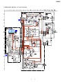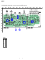
1
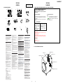
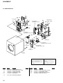
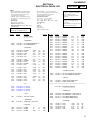
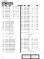
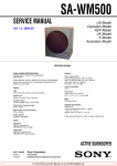
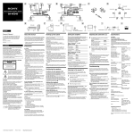
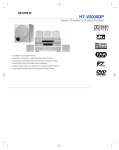
SA-WMS367
SERVICE MANUAL
US Model
Canadian Model
Ver 1.0 2004.03
• SA-WMS367 is the subwoofer
section in SA-VE367T.
SPECIFICATIONS
For the US model
AUDIO POWER SPECIFICATIONS
POWER OUTPUT AND TOTAL HARMONIC
DISTORTION:
with 6 ohm loads, from 20 - 200 Hz; rated 120 watts per
channel minimum RMS power, with no more than 10%
total harmonic distortion from 250 milliwatts to rated
output.
Speaker system
Active subwoofer,
magnetically shielded
Speaker unit
Woofer: 20 cm (8 in.)
Enclosure type
Acoustically loaded
Bass Reflex
Reproduction frequency range
26 Hz - 200 Hz
Continuous RMS power output
135 W (6 ohms, 100 Hz,
10% THD)
Inputs
INPUT (input pin jack)
SPEAKER IN (input terminals)
Outputs
SPEAKER OUT (output terminals)
General
Power requirements
Power consumptions
Dimensions (w/h/d)
Mass
120 V AC, 60 Hz
130 W
1 W (standby mode)
Approx. 290 × 400 × 424 mm
(11 1/8 × 15 1/4 × 16 3/8 in.)
Approx. 13 kg
(28 lb 11 oz)
Design and specifications are subject to change without
notice.
SUBWOOFER
9-877-698-01
Sony Corporation
2004C04-1
© 2004.03
Home Audio Company
Published by Sony Engineering Corporation
1
SA-WMS367
SAFETY CHECK-OUT
After correcting the original service problem, perform the following safety check before releasing the set to the customer:
Check the antenna terminals, metal trim, “metallized” knobs, screws,
and all other exposed metal parts for AC leakage.
Check leakage as described below.
LEAKAGE TEST
The AC leakage from any exposed metal part to earth ground and
from all exposed metal parts to any exposed metal part having a
return to chassis, must not exceed 0.5 mA (500 microampers.).
Leakage current can be measured by any one of three methods.
1. A commercial leakage tester, such as the Simpson 229 or RCA
WT-540A. Follow the manufacturers’ instructions to use these
instruments.
2. A battery-operated AC milliammeter. The Data Precision 245
digital multimeter is suitable for this job.
3. Measuring the voltage drop across a resistor by means of a
VOM or battery-operated AC voltmeter. The “limit” indication is 0.75 V, so analog meters must have an accurate lowvoltage scale. The Simpson 250 and Sanwa SH-63Trd are examples of a passive VOM that is suitable. Nearly all battery
operated digital multimeters that have a 2 V AC range are suitable. (See Fig. A)
TABLE OF CONTENTS
1. GENERAL
Location of Controls ................................................................ 3
2. DIAGRAMS
2-1. Note for Printed Wiring Boards and
Schematic Diagrams ............................................................ 3
2-2. Circuit Boards Location ...................................................... 3
2-3. Printed Wiring Boards – Main Section – ............................ 4
2-4. Schematic Diagram – Main Section – ................................. 5
2-5. Printed Wiring Boards – Control Section – ......................... 6
2-6. Schematic Diagram – Control Section – ............................. 7
2-7. IC Block Diagram ............................................................... 8
3. EXPLODED VIEWS
3-1. Front Section ....................................................................... 9
3-2. Rear Section ...................................................................... 10
4. ELECTRICAL PARTS LIST ......................................... 11
To Exposed Metal
Parts on Set
0.15 µF
1.5 k Ω
AC
voltmeter
(0.75 V)
Earth Ground
(Fig. A)
SAFETY-RELATED COMPONENT WARNING!!
COMPONENTS IDENTIFIED BY MARK 0 OR DOTTED LINE
WITH MARK 0 ON THE SCHEMATIC DIAGRAMS AND IN
THE PARTS LIST ARE CRITICAL TO SAFE OPERATION.
REPLACE THESE COMPONENTS WITH SONY PARTS WHOSE
PART NUMBERS APPEAR AS SHOWN IN THIS MANUAL OR
IN SUPPLEMENTS PUBLISHED BY SONY.
2
SOLDER
• UNLEADED
Boards requiring use of unleaded solder are printed with the leadfree mark (LF) indicating the solder contains no lead.
(Caution: Some printed circuit boards may not come printed with
the lead free mark due to their particular size.)
: LEAD FREE MARK
Unleaded solder has the following characteristics.
• Unleaded solder melts at a temperature about 40°C higher than
ordinary solder.
Ordinary soldering irons can be used but the iron tip has to be
applied to the solder joint for a slightly longer time.
Soldering irons using a temperature regulator should be set to
about 350°C.
Caution: The printed pattern (copper foil) may peel away if
the heated tip is applied for too long, so be careful!
• Strong viscosity
Unleaded solder is more viscous (sticky, less prone to flow)
than ordinary solder so use caution not to let solder bridges
occur such as on IC pins, etc.
• Usable with ordinary solder
It is best to use only unleaded solder but unleaded solder may
also be added to ordinary solder.
ATTENTION AU COMPOSANT AYANT RAPPORT
À LA SÉCURITÉ!!
LES COMPOSANTS IDENTIFIÉS PAR UNE MARQUE 0 SUR LES
DIAGRAMMES SCHÉMATIQUES ET LA LISTE DES PIÈCES SONT
CRITIQUES POUR LA SÉCURITÉ DE FONCTIONNEMENT. NE
REMPLACER CES COMPOSANTS QUE PAR DES PIÈCES SONY
DONT LES NUMÉROS SONT DONNÉS DANS CE MANUEL OU
DANS LES SUPPLÉMENTS PUBLIÉS PAR SONY.
SA-WMS367
SECTION 1
GENERAL
LOCATION OF CONTROL
A
Front (Right) Subwoofer
2-1. NOTE FOR PRINTED WIRING BOARDS AND SCHEMATIC DIAGRAMS
Center
Front (Left)
Ee
Ee
B
Front (Right)
Center
C
Front (Left)
THIS NOTE IS COMMON FOR PRINTED WIRING
BOARDS AND SCHEMATIC DIAGRAMS.
(In addition to this, the necessary note is printed
in each block.)
Ee
Ee
INPUT
Ee
Ee
e
3.5 m
(11.5 ft.)
3.5 m
(11.5 ft.)
3.5 m
(11.5 ft.)
3.5 m
(11.5 ft.)
FRONT
E
e
eE Ee
R
CENTER
L
L
R
R
2.5m (8.2 ft.)
FRONT
SPEAKER SPEAKER
IN
OUT
Ee
Surround back
(Right)
Surround back
(Left)
Ee
Ee
Surround (Right)
Surround back
(Right)
Surround back
(Left)
E
Center
E
Ee
Ee
Surround (Left)
e
E
10m
(32.8 ft.)
10m
(32.8 ft.)
Ee
Subwoofer
SURROUND
SURROUND BACK
Ee
e
E
e
E
R
L
10 m
(32.8 ft.)
Ee
3.5 m
(11.5 ft.)
L
e
E
E
e
L
eE Ee
L R
SURROUND
SURROUND BACK
10 m
(32.8 ft.)
D
E
e
eE Ee
Amplifier
eE Ee
L R
WOOFER OUT
Surround (Right)
L
2.5m (8.2 ft.)
3.5 m
(11.5 ft.)
R
CENTER
Amplifier
Surround (Left)
F
G
Subwoofer
Foot pads
Front (Right)
Front (Left)
30
100
WS-WV10D
(for surround
speakers)
30
~ 120
100
WS-FV11
~ 120
Foot pads
A
For schematic diagrams.
For printed wiring boards.
Note:
• All capacitors are in µF unless otherwise noted. pF: µµF
50 WV or less are not indicated except for electrolytics
and tantalums.
• All resistors are in Ω and 1/4 W or less unless otherwise
specified.
f
: internal component.
•
• C : panel designation.
Note:
• X : parts extracted from the component side.
• Y : parts extracted from the conductor side.
•
: Pattern from the side which enables seeing.
• Abbreviation
CND : Canadian model.
A
Note:
The components identified by mark 0 or dotted
line with mark 0 are critical for safety.
Replace only with part
number specified.
A
Surround (Right)
Surround (Left)
Surround back
(Left)
SECTION 2
DIAGRAMS
This section is extracted
from instruction manual.
Surround back
(Right)
H
I
J
K
+
POWER
POWER
indicator
+
POWER SAVE
INPUT
AUTO
POWER
INPUT
VOLUME
OFF
MAX
VOLUME
Note:
Les composants identifiés par
une marque 0 sont critiques
pour la sécurité.
Ne les remplacer que par une
piéce por tant le numéro
spécifié.
MIN
BASS BOOST
• A : B+ Line.
• B : B– Line.
• Voltages are dc with respect to ground under no-signal
(detuned) conditions.
no mark : Power on
• Voltages are taken with a VOM (Input impedance 10 MΩ).
Voltage variations may be noted due to normal production tolerances.
• Signal path.
F : AUDIO
• Abbreviation
CND : Canadian model.
MAX
BASS BOOST
MIN
PHASE
NORMAL
REVERSE
PHASE
POWER SAVE
AUTO
OFF
About this manual
Hooking up the system
Setting the amplifier
The SA-VE367T is a 7.1 channel speaker system
consisting of two front speakers, two surround speakers,
two surround back speakers, one center speaker, and one
subwoofer. It supports Sony Digital Cinema Sound,
Dolby* Pro Logic, and Dolby Digital etc., and is thus
geared towards the enjoyment of movies.
Connect the speaker system to the speaker output
terminals of an amplifier.
Make sure power to all components (included the
subwoofer) is turned off before starting the hook-up.
When connecting to an amplifier with internal multi
channel decoders (Dolby Digital, DTS**, etc.), you should
use the setup menus for the amplifier to specify the
parameters of your speaker system.
See the table below for the proper settings. For details on
the setting procedure, refer to the manual that was
provided with your amplifier.
* “Dolby” and the double-D symbol are trademarks of
Dolby Laboratories.
Precautions
On safety
• Before operating the system, be sure that the operating
voltage of the system is identical with that of your local
power supply.
• The unit is not disconnected from the AC power source
(mains) as long as it is connected to the wall outlet,
even if the unit itself has been turned off.
• Unplug the system from the wall outlet if it is not to be
used for an extended period of time. To disconnect the
cord, pull the cord by grasping the plug. Never pull
the cord itself.
• Should any liquid or solid object fall into the system,
unplug the system’s power cord and have the system
checked by qualified personnel before operating it any
further.
• AC power cord must be changed only at the qualified
service shop.
On operation
• Do not drive the speaker system with a continuous
wattage exceeding the maximum input power of the
system.
• If the polarity of the speaker connections are not
correct, the bass tones will be weak and the position of
the various instruments obscure.
• Contact between bare speaker wires at the speaker
terminals may result in a short-circuit.
• Before connecting, turn off the amplifier to avoid
damaging the speaker system.
• The speaker grille cannot be removed. Do not attempt
to remove the grille on the speaker system. If you try
to remove it, you may damage the speaker.
• The volume level should not be turned up to
the point of distortion.
If you encounter color irregularity on a
nearby TV screen
This speaker system is magnetically shielded to allow it
to be installed near a TV set. However, color
irregularities may still be observed on certain types of TV
sets.
If color irregularity is observed...
c Turn off the TV set, then turn it on again after 15 to
30 minutes.
If color irregularity is observed again...
c Place the speakers further away from the TV set.
If howling occurs
Reposition the speakers or turn down the volume on the
amplifier.
On placement
• Do not set the speakers in an inclined position.
• Do not place the speakers in locations that are:
— Extremely hot or cold
— Dusty or dirty
— Very humid
— Subject to vibrations
— Subject to direct sunlight
• Use caution when placing the speaker on a specially
treated (waxed, oiled, polished, etc.) floor, as staining
or discoloration may result.
On cleaning
Clean the speaker cabinets with a soft cloth lightly
moistened with a mild detergent solution or water. Do
not use any type of abrasive pad, scouring powder or
solvent such as alcohol or benzine.
HookupA
Usually, connect by this method.
This configuration is used when the amplifier is
connected to a DVD player, LD player, VCR or other
video devices.
HookupB
Try this configuration instead of “Hookup A” when
there are no jacks on the amplifier for a subwoofer.
An optional specified speaker cord (2.5 m × 2)(8.2 ft. × 2)
is necessary when connecting this way.
Notes (C)
• Make sure the plus (+) and the minus (–) terminals on
the speakers are matched to the corresponding plus (+)
and minus (–) terminals on the amplifier.
• Be sure to tighten the screws of the speaker terminals
securely as loose screws may become a source of noise.
• Make sure all connections are firm. Contact between
bare speaker wires at the speaker terminals may cause
a short-circuit.
• For details regarding the connections on the amplifier
side, refer to the manual that was provided with your
amplifier.
Tip
Black or black striped wires are minus (–) in polarity, and
should be connected to the minus (–) speaker terminals.
Positioning the speakers
Location of each speaker (D)
Each speaker should face the listening position. Better
surround effect will result if all speakers are set at the
same distance from the listening position.
Place the front speakers at a suitable distance to the left
and right of the television.
Place the subwoofer on either side of the television.
Place the center speaker on the top-center of the TV set.
The placement of surround speakers greatly depends on
the configuration of the room. The surround speakers
may be placed slightly behind the listening position.
Place the surround back speakers behind the listening
position. The angle A should be the same.
Setting the speakers
To prevent speaker vibration or movement while
listening, attach the supplied foot pads to the bottom
four corners of the center speaker, front speakers,
surround speakers and surround back speakers (E).
When “Hookup A” is used
(Speaker setup)
For
Set to
Front speakers
SMALL
Center speaker
SMALL
Surround speakers
SMALL
Subwoofer
ON (or YES)
When “Hookup B” is used
(Speaker setup)
Set the volume level to best suit your
preference according to the program
source.
2
Select the phase polarity.
Use the PHASE selector to select the phase
polarity.
3
Set BASS-BOOST to MIN.
Rotate BASS-BOOST according to the
output level that you prefer. Some
material is recorded with strong emphasis
on bass sounds, which may be accessive in
some cases. If this happens, rotate BASSBOOST towards minimum.
Set to
LARGE
Center speaker
SMALL
Notes
Surround speakers
SMALL
Subwoofer
OFF (or NO)
• Some amplifier functions for enhancing the sound may
cause distortion in the subwoofer. If such distortion
occurs, turn off those functions.
• To enjoy high-quality sound, do not turn the
subwoofer volume too high.
• If the sound distorts when you turn on the bass
reinforcement from your amplifier (such as DBFB,
GROOVE, the graphic equalizer, etc.), turn down the
bass reinforcement and adjust the level.
• Do not turn the LEVEL knob to maximum. Doing so
may weaken the bass sound. Moreover, extraneous
noise may be heard.
• Selecting NORMAL or REVERSE with the PHASE
selector reverses the polarity and may provide better
bass reproduction in certain listening environments
(depending on the type of front speakers, the position
of the subwoofer and the adjustment of the BASSBOOST. It may also change the expansion and
tightness of sound, and effect the feeling of the sound
field. Select the setting that provides the sound you
prefer when listening in your normal listening position.
If you use the amplifier with adjustable crossover
frequency, it is recommended to select 150 Hz (or close to
this figure) as the crossover frequency for your front,
center, and surround speakers.
** “DTS” and “DTS Digital Surround” are registered
trademarks of Digital Theater Systems, Inc.
Listening to the sound ( I)
First, turn down the volume on the amplifier. The
volume should be set to minimum before you begin
playing the program source.
1
Turn on the amplifier and select the
program source.
2
Press POWER on the subwoofer.
The POWER indicator on the subwoofer
lights up green.
3
Play the program source.
Power turns on and off automatically — Auto
power on/off function (J)
Tip
Note
The height of the front speakers should be adjusted to
about the center of the TV screen ( H).
If you turn down the volume level of the amplifier too
low, the auto power on/off function may activate,
causing the subwoofer to enter power saving mode.
Setting other speakers (G)
Rotate VOLUME to adjust the volume.
Front speakers
For greater flexibility in the positioning of the speakers,
use the optional WS-FV11 or WS-WV10D speaker stand
(available only in certain countries).
Set the center speaker firmly on top of the TV set, making
sure it is completely level.
1
For
When the subwoofer is on (i.e, the POWER indicator
lights up green) and there is no signal input for a few
minutes, the POWER indicator changes to red and the
subwoofer enters power saving mode. While in this
mode a signal is input to the subwoofer, the subwoofer
automatically turns on (auto power on/off function).
To turn this feature off, slide the POWER SAVE switch
on the rear panel to OFF.
Setting the center speaker (F)
Adjusting the subwoofer ( K)
2-2. CIRCUIT BOARDS LOCATION
TERMINAL board
MAIN board
CONTROL board
POWER SWITCH board
Troubleshooting
Should you encounter a problem with your speaker
system, check the following list and take the indicated
measures. If the problem persists, consult your nearest
Sony dealer.
POWER AMP board
There is no sound from the speaker system.
• Make sure all the connections have been
correctly made.
• Make sure the volume on the amplifier has
been turned up properly.
• Make sure the program source selector on the
amplifier is set to the proper source.
• Check if headphones are connected. If they
are, disconnect them.
POWER SUPPLY board
There is distortion in the subwoofer sound
output.
• Check if any sound-enhancing functions have
been activated on the amplifier. If they have,
turn them off.
There is hum or noise in the speaker output.
• Make sure all the connections have been
correctly made.
• Make sure none of the audio components are
positioned too close to the TV set.
The sound has suddenly stopped.
• Make sure all the connections have been
correctly made. Contact between bare
speaker wires at the speaker terminals may
cause a short-circuit.
If you have any questions or problems concerning your
speaker system, please consult your nearest Sony dealer.
3
3
SA-WMS367
2-3. PRINTED WIRING BOARDS — MAIN SECTION — • Refer to page 3 for Circuit Boards Location.
1
2
3
4
5
6
: Uses unleaded solder.
7
8
9
10
11
12
13
14
(Page 6)
A
R701
R703
C713
JW711
Q702
C703
R702
R706
R715
R717
C708
C701
R716
C702
BC901
JW707
C704
R708
JW709
R712
JW703
JW702
R709
R714
IC701
CN1
(Page 6)
JW053
F11
RY901
D
C709
D702
C902
C901
C711
C707
C712
R704
C710
C705
D701
CN701
JW701
R713
JW704 CN702
JW705
C
Q701
JW052
T202
BC902
JW051
R711
B
C706
R705
BC903
C716
JW708
R707
R710
D703
T102
SP401
F901
F12
D901
D401
BC401
C401
JW827
R402
Q402
J
Q403
C402
JW829
JW828
C801
R401
C803
D805
C805
C804
BC801
JW833
R406
JW808
R540
Q534
R542
R541
Q535
JW823
R535
R534
R533
R539
R537
IC530
R532
JW820
JW821
Q532
Q533
R536
JW822
JW824
C307
BC803
JW819
JW818
R105
Q104
R103
JW834
R101
R102
C308
D532
R538
D531
R531
R104
Q105
Q102
JW816
JW807
4
R106
D305
Q103
Q101
Q301
D304
D203
C532
JW825
C102
D303
C304
C101
JW826
C802
R303
4
Q531
R800
C531
Q302
D302
S201
JW835
JW814
JW837
D306
D301
C306
C302
C201
CN804
JW813
C305
C301
BC802
JW302
JW805
BC202
JW804
JW301
JW817
H-11
H-11
H-11
I-12
H-11
H-9
H-9
F-11
E-11
F-12
E-12
G-13
I-12
H-13
I-12
I-11
C-8
C-12
C403
CN805
JW810
Q101
Q102
Q103
Q104
Q105
Q301
Q302
Q401
Q402
Q403
Q404
Q531
Q532
Q533
Q534
Q535
Q701
Q702
R404
R400
R304
JW809
H-13
C-10
RY400
D533
I
IC530
IC701
JW832
JW802
C303
H
Q401
JW812
JW811
G
G2
JW830
R405
R403
C806
BC203
F
• Semiconductor
Location
Ref. No. Location
D203
I-3
D301
H-8
D302
H-8
D303
H-8
D304
I-8
D305
H-9
D306
H-9
D400
F-12
D401
E-8
D531
H-12
D532
G-13
D533
I-12
D701
B-9
D702
B-9
D703
B-8
D805
F-8
D901
E-4
JW801
G1
Q404
D400
CN904
E
SA-WMS367
2-4. SCHEMATIC DIAGRAM — MAIN SECTION — • Refer to page 8 for IC Block Diagram.
D532
Q535
D533
R532
R540
R535
BC803
CN804
R533
D203
Q532
R538
IC530(2/2)
C531
S201
BC203
D531
Q534
R537
C201
R541
BC202
R542
C532
Q531
(Page 7)
R534
R539
IC530(1/2)
R531
R536
BC902
Q533
RY901
Q301
D901
C902
D302
R303
D305
F901
T202
C303
C307
IC B/D
IC701
BC901
D301
C305
C301
BC802
CN904
CN1
C901
C306
D306
C308
R304
R701
C701
R715
D701
C702
C705
D304
C304
C302
D303
C806
C713
BC903
Q302
D702
R716
R702
R708
R705
R714
C710
R707
C703
Q702
R703
C804
R717
R704
D805
C704
C706
C802
CN701
T102
BC801
CN905
C801
R800
R712
C805
C803
Q104
CN805
R706
C716
R102
R105
C711
C708
Q101
C707
R103
C709
C101
R101
Q102
C102
R709
Q103
R106
Q701
R710
R711
D703
Q105
R713
Q404
R403
R404
R402
D401
R401
BC401
Q402
Q401
C403
Q403
SP401
RY400
C402
R406
D400
(Page 7)
R104
C712
CN702
C401
R405
5
5
R400
CN102
SA-WMS367
2-5. PRINTED WIRING BOARDS — CONTROL SECTION — • Refer to page 3 for Circuit Boards Location.
1
2
3
4
5
6
: Uses unleaded solder.
7
8
10
11
12
13
14
J601
A
TM501
R612
R615
R613
R601
Q601
B-1
JW601
R620
JW603
R605
(Page 4)
6
6
R607
JW514
JW502
R514
R513
R501
R509
JW505
R507
C501
D501
D502
R502
R504
R510
C504
D504
C503
IC501
JW513
JW515
C502
D503
JW512
C505
R508
JW501
R511
JW511
IC601
C605
JW602
R604
R621
R606
JW605
BC601
• Semiconductor
Location
Ref. No. Location
D501
C-12
D502
C-12
D503
C-12
D504
C-12
C-11
C-8
C-2
C-4
B-6
JW509
BC602
C618
JW611
R614
R619
JW616
C613
R622
(Page 4)
IC501
IC601
IC602
IC603
IC604
JW600 JW508
JW510
R623
C614
C607
E
JW612
JW606
R603
JW610
C617
C612
R609
JW607
D
R602
R506
R503
RV601
R505
JW507
R512
RV602
JW670
JW613
C609
JW608
C606
JW506
C602
C604
IC602
C608
JW517
JW516
JW500
IC603
JW614
R618
C603
R611
R610
R617
JW604
C619
R616
R608
Q601
C610
C601
C616
IC604
C611
B
JW615
C615
JW609
S602
JW504
S601
C
9
SA-WMS367
2-6. SCHEMATIC DIAGRAM — CONTROL SECTION —
D501
D503
TM501
R501
R505
IC501(1/2)
C502
R502
R510
D502
D504
C503
R504
R511
R506
IC501(2/2)
R503
C504
C501
R507
R508
R509
R513
R512
R514
C505
BC601
R604
R605
IC604(2/2)
IC601(1/2)
IC601(2/2)
IC602(1/2)
R606
C612
C613
R612
R616 R617
IC603(1/2)
IC603(2/2)
C619
J601
R601
C615
IC602(2/2)
R607
R603
C617
R610
RV601
(Page 5)
R621
R613
C602
C601
C614
C603
R602
R622
R623
C618
IC604(1/2)
BC602
RV602
C604
C610
C611
C605
S602
Q601
R619
(Page 5)
R608
R614
S601
R609
C606
C607 C608
R611
R615
R618
C609
7
C616
7
R620
SA-WMS367
2-7. IC BLOCK DIAGRAM
IC701 STK404-130S (POWER AMP Board)
1
2
3
4
5
6
7
8
9
10
11
12
13
8
8
SA-WMS367
SECTION 3
EXPLODED VIEWS
NOTE:
• The mechanical parts with no reference
number in the exploded views are not supplied.
• Items marked “*” are not stocked since
they are seldom required for routine service.
Some delay should be anticipated
when ordering these items.
• -XX and -X mean standardized parts, so
they may have some difference from the
original one.
• Color Indication of Appearance Parts
Example :
KNOB, BALANCE (WHITE) ... (RED)
R
R
Parts Color Cabinet’s Color
• Accessories are given in the last of this
parts list.
• Abbreviation
CND : Canadian model
The components identified by
mark 0 or dotted line with mark
0 are critical for safety.
Replace only with part number
specified.
Les composants identifiés par une
marque 0 sont critiques pour
la sécurité.
Ne les remplacer que par une piéce
portant le numéro spécifié.
3-1. FRONT SECTION
not supplied
(POWER SWITCH board)
#1
7
#1
SP401
6
5
not supplied
4
not supplied
5
1
2
3
3
2
3
3
2
Ref. No.
1
2
3
4
5
Part No.
Description
4-254-094-01
4-981-864-01
4-235-677-01
4-253-282-01
4-874-614-02
BOTTOM (PANEL)
FOOT
SCREW (4X20) (TYPE1), +BVTP
PUSH (KNOB)
SCREW (1) (3.5X14), TAPPING
Remark
Ref. No.
6
7
SP401
#1
3
2
3
Part No.
Description
4-254-093-01
4-254-092-01
1-825-151-21
7-685-647-79
GRILLE (FRAME)
WOOFER (RING)
SPEAKER (20cm) (WOOFER)
SCREW +BVTP 3X10 TYPE2 IT-3
Remark
9
SA-WMS367
3-2. REAR SECTION
#1
52
#1
56
not supplied
#2
#2
not supplied
(TERMINAL board)
52
supplied with
RV601, RV602
52
#1
52
57
T102
52
55
54
52
#1
not supplied
(CONTROL board)
52
52
F901
#1
53
#1
#1
A
not supplied
not supplied
(POWER SUPPLY board)
not supplied
not supplied
(POWER AMP board)
A
52
not supplied
51
The components identified by
mark 0 or dotted line with mark
0 are critical for safety.
Replace only with part number
specified.
Ref. No.
Part No.
Description
51
52
53
* 54
0 55
A-4714-295-A
4-235-677-01
3-905-609-31
3-703-244-00
1-783-820-11
SPEAKER (CABINET) ASSY
SCREW (4X20) (TYPE1), +BVTP
SCREW (TRANSISTOR)
BUSHING (2104), CORD
CORD, POWER
56
10
A-4751-446-A MAIN BOARD, COMPLETE
Remark
Les composants identifiés par une
marque 0 sont critiques pour
la sécurité.
Ne les remplacer que par une piéce
portant le numéro spécifié.
Ref. No.
Part No.
Description
57
0 F901
0 T102
#1
#2
4-999-482-81
1-532-745-11
1-443-275-11
7-685-647-79
7-685-880-09
KNOB (VOL)
FUSE, GLASS TUBE (3.15A/125V)
TRANSFORMER, POWER
SCREW +BVTP 3X10 TYPE2 IT-3
SCREW +BVTT 4X6 (S)
Remark
SA-WMS367
SECTION 4
ELECTRICAL PARTS LIST
NOTE:
• Due to standardization, replacements in
the parts list may be different from the
parts specified in the diagrams or the
components used on the set.
• -XX and -X mean standardized parts, so
they may have some difference from the
original one.
• RESISTORS
All resistors are in ohms.
METAL:Metal-film resistor.
METAL OXIDE: Metal oxide-film resistor.
F:nonflammable
• Items marked “*” are not stocked since
they are seldom required for routine service.
Some delay should be anticipated
when ordering these items.
• SEMICONDUCTORS
In each case, u : µ, for example:
uA.. : µA.. uPA.. : µPA..
uPB.. : µPB.. uPC.. : µPC.. uPD.. : µPD..
• CAPACITORS
uF : µF
• COILS
uH : µH
• Abbreviation
CND : Canadian model
When indicating parts by reference
number, please include the board.
Ref. No.
Part No.
Description
Remark
CONTROL BOARD
***************
< CONNECTOR >
BC601
BC602
1-691-769-11 PLUG (MICRO CONNECTOR) 7P
1-564-505-11 PLUG, CONNECTOR 2P
< CAPACITOR >
C601
C602
C603
C604
C605
1-102-978-00
1-126-964-11
1-126-964-11
1-136-165-00
1-136-165-00
CERAMIC
ELECT
ELECT
FILM
FILM
220PF
10uF
10uF
0.1uF
0.1uF
5%
20%
20%
5%
5%
50V
50V
50V
50V
50V
C606
C607
C608
C609
C610
1-126-964-11
1-164-159-11
1-126-964-11
1-164-159-11
1-131-698-31
ELECT
CERAMIC
ELECT
CERAMIC
FILM
10uF
0.1uF
10uF
0.1uF
0.33uF
20%
5%
50V
50V
50V
50V
50V
C611
C612
C613
C614
C615
1-131-695-11
1-131-696-11
1-131-696-11
1-126-963-11
1-131-696-11
FILM
FILM
FILM
ELECT
FILM
0.18uF
0.22uF
0.22uF
4.7uF
0.22uF
5%
5%
5%
20%
5%
50V
50V
50V
50V
50V
C616
C617
C618
C619
1-131-688-31
1-126-965-11
1-126-963-11
1-126-965-11
FILM
ELECT
ELECT
ELECT
0.047uF
22uF
4.7uF
22uF
5%
20%
20%
20%
50V
50V
50V
50V
20%
< IC >
IC601
IC602
IC603
IC604
8-759-943-94
8-759-943-94
8-759-943-94
8-759-943-94
IC
IC
IC
IC
MAIN
The components identified by
mark 0 or dotted line with mark
0 are critical for safety.
Replace only with part number
specified.
Les composants identifiés par une
marque 0 sont critiques pour
la sécurité.
Ne les remplacer que par une piéce
portant le numéro spécifié.
Part No.
Description
R604
R605
R606
R607
R608
1-249-415-11
1-247-847-11
1-247-847-11
1-249-429-11
1-247-843-11
CARBON
CARBON
CARBON
CARBON
CARBON
680
4.7K
4.7K
10K
3.3K
5%
5%
5%
5%
5%
1/4W
1/4W
1/4W
1/4W
1/4W
R609
R610
R611
R612
R613
1-249-439-11
1-247-831-11
1-247-871-11
1-249-429-11
1-247-879-11
CARBON
CARBON
CARBON
CARBON
CARBON
68K
1K
47K
10K
100K
5%
5%
5%
5%
5%
1/4W
1/4W
1/4W
1/4W
1/4W
R614
R615
R616
R617
R618
1-249-431-11
1-249-436-11
1-249-428-11
1-249-428-11
1-247-879-11
CARBON
CARBON
CARBON
CARBON
CARBON
15K
39K
8.2K
8.2K
100K
5%
5%
5%
5%
5%
1/4W
1/4W
1/4W
1/4W
1/4W
R619
R620
R621
R622
R623
1-247-879-11
1-247-847-11
1-249-429-11
1-249-429-11
1-249-429-11
CARBON
CARBON
CARBON
CARBON
CARBON
100K
4.7K
10K
10K
10K
5%
5%
5%
5%
5%
1/4W
1/4W
1/4W
1/4W
1/4W
Remark
< VARIABLE RESISTOR >
RV601
RV602
1-227-661-11 RES, VAR, CARBON 10K (BASS BOOST)
1-225-826-11 RES, VAR, CARBON 20K (VOLUME)
< SWITCH >
S601
1-786-490-11 SWITCH, SLIDE (POWER SAVE)
S602
1-786-490-11 SWITCH, SLIDE (PHASE)
*************************************************************
BA15218
BA15218
BA15218
BA15218
A-4751-446-A MAIN BOARD, COMPLETE
*********************
< CONNECTOR >
< JACK >
J601
Ref. No.
CONTROL
BC401
* BC801
BC802
BC803
1-815-025-11 JACK, PIN 1P (INPUT)
1-564-320-00
1-564-104-00
1-691-767-11
1-691-765-11
PIN, CONNECTOR (3.96mm PITCH) 2P
PIN, CONNECTOR (3.96mm PITCH) 3P
PLUG (MICRO CONNECTOR) 5P
PLUG (MICRO CONNECTOR) 3P
< TRANSISTOR >
< CAPACITOR >
Q601
8-729-119-78 TRANSISTOR 2SC2785-HFE
< RESISTOR >
R601
R602
R603
1-247-831-11 CARBON
1-247-831-11 CARBON
1-247-879-11 CARBON
1K
1K
100K
5%
5%
5%
1/4W
1/4W
1/4W
C101
C102
C301
C302
C303
1-126-933-11
1-126-933-11
1-136-165-00
1-136-165-00
1-104-666-11
ELECT
ELECT
FILM
FILM
ELECT
100uF
100uF
0.1uF
0.1uF
220uF
20%
20%
5%
5%
20%
16V
16V
50V
50V
25V
11
SA-WMS367
MAIN
Ref. No.
POWER AMP
Part No.
Description
C304
C305
C306
C307
C308
1-104-666-11
1-126-964-11
1-126-964-11
1-124-247-11
1-124-247-11
ELECT
ELECT
ELECT
ELECT
ELECT
220uF
10uF
10uF
10uF
10uF
20%
20%
20%
20%
20%
25V
50V
50V
35V
35V
Remark
C401
C402
C403
C531
C532
1-124-257-00
1-126-950-11
1-126-923-11
1-104-662-11
1-104-661-11
ELECT
ELECT
ELECT
ELECT
ELECT
2.2uF
330uF
220uF
22uF
330uF
20%
20%
20%
20%
20%
35V
35V
10V
25V
16V
C801
C802
C803
C804
C805
1-165-946-11
1-165-946-11
1-130-777-00
1-130-777-00
1-162-199-31
ELECT
ELECT
FILM
FILM
CERAMIC
6800uF
6800uF
0.1uF
0.1uF
10PF
20%
20%
5%
5%
5%
71V
71V
50V
50V
50V
C806
1-162-199-31 CERAMIC
10PF
5%
50V
< DIODE >
D301
D302
D303
D304
D305
8-719-024-99
8-719-024-99
8-719-024-99
8-719-024-99
8-719-110-31
DIODE
DIODE
DIODE
DIODE
DIODE
11ES2-NTA2B
11ES2-NTA2B
11ES2-NTA2B
11ES2-NTA2B
RD12ESB2
D306
D400
D401
D531
D532
8-719-110-31
8-719-991-33
8-719-991-33
8-719-991-33
8-719-991-33
DIODE
DIODE
DIODE
DIODE
DIODE
RD12ESB2
1SS133T-77
1SS133T-77
1SS133T-77
1SS133T-77
D533
D805
8-719-991-33 DIODE 1SS133T-77
8-719-072-05 DIODE RBV-602LF-A
Ref. No.
Part No.
Description
Remark
< RESISTOR >
R101
R102
R103
R104
R105
1-247-863-11
1-247-863-11
1-249-427-11
1-249-427-11
1-247-843-11
CARBON
CARBON
CARBON
CARBON
CARBON
22K
22K
6.8K
6.8K
3.3K
5%
5%
5%
5%
5%
1/4W
1/4W
1/4W
1/4W
1/4W
R106
R303
R304
0 R400
R401
1-247-843-11
1-249-421-11
1-249-421-11
1-215-869-11
1-249-430-11
CARBON
CARBON
CARBON
METAL OXIDE
CARBON
3.3K
2.2K
2.2K
1K
12K
5%
5%
5%
5%
5%
1/4W
1/4W
1/4W
1W
F
1/4W
R402
R403
R404
R405
R406
1-247-873-11
1-247-879-11
1-247-879-11
1-247-863-11
1-247-863-11
CARBON
CARBON
CARBON
CARBON
CARBON
56K
100K
100K
22K
22K
5%
5%
5%
5%
5%
1/4W
1/4W
1/4W
1/4W
1/4W
R531
R532
R533
R534
R535
1-247-895-00
1-247-883-00
1-247-903-00
1-247-879-11
1-249-429-11
CARBON
CARBON
CARBON
CARBON
CARBON
470K
150K
1M
100K
10K
5%
5%
5%
5%
5%
1/4W
1/4W
1/4W
1/4W
1/4W
R536
R537
R538
R539
R540
1-249-429-11
1-247-879-11
1-247-903-00
1-247-863-11
1-249-421-11
CARBON
CARBON
CARBON
CARBON
CARBON
10K
100K
1M
22K
2.2K
5%
5%
5%
5%
5%
1/4W
1/4W
1/4W
1/4W
1/4W
R541
R542
R800
1-249-421-11 CARBON
1-247-831-11 CARBON
1-247-873-11 CARBON
2.2K
1K
56K
5%
5%
5%
1/4W
1/4W
1/4W
< RELAY >
< GROUND TERMINAL >
G1
G2
1-537-738-21 TERMINAL, GROUND
1-537-738-21 TERMINAL, GROUND
RY400 1-515-920-11 RELAY (24V)
*************************************************************
POWER AMP BOARD
*****************
< IC >
IC530
6-704-502-01 IC NJM022D
< CAPACITOR >
< TRANSISTOR >
Q101
Q102
Q103
Q104
Q105
8-729-029-86
8-729-029-86
8-729-029-40
8-729-119-76
8-729-119-78
TRANSISTOR
TRANSISTOR
TRANSISTOR
TRANSISTOR
TRANSISTOR
DTC124ESA
DTC124ESA
DTA124ESA
2SA1175-HFE
2SC2785-HFE
Q301
Q302
Q401
Q402
Q403
8-729-281-53
8-729-201-53
8-729-119-78
8-729-178-42
8-729-119-78
TRANSISTOR
TRANSISTOR
TRANSISTOR
TRANSISTOR
TRANSISTOR
2SC1815-GR
2SA1015-GR
2SC2785-HFE
2SC2784-F
2SC2785-HFE
Q404
Q531
Q532
Q533
Q534
8-729-029-86
8-729-029-86
8-729-119-76
8-729-029-86
8-729-900-63
TRANSISTOR
TRANSISTOR
TRANSISTOR
TRANSISTOR
TRANSISTOR
DTC124ESA
DTC124ESA
2SA1175-HFE
DTC124ESA
DTA124ES
Q535
8-729-900-63 TRANSISTOR DTA124ES
C701
C702
C703
C704
C705
1-102-978-00
1-102-978-00
1-128-562-11
1-102-936-00
1-126-961-11
CERAMIC
CERAMIC
ELECT
CERAMIC
ELECT
220PF
220PF
47uF
3PF
2.2uF
5%
5%
20%
0.25PF
20%
50V
50V
100V
50V
50V
C706
C707
C708
C709
C710
1-104-666-11
1-128-563-11
1-128-582-11
1-104-665-11
1-102-824-00
ELECT
ELECT
ELECT
ELECT
CERAMIC
220uF
100uF
10uF
100uF
470PF
20%
20%
20%
20%
5%
25V
100V
100V
25V
50V
C711
C712
C713
C716
1-128-582-11
1-136-165-00
1-102-978-00
1-162-199-31
ELECT
FILM
CERAMIC
CERAMIC
10uF
0.1uF
220PF
10PF
20%
5%
5%
5%
100V
50V
50V
50V
< CONNECTOR >
CN701
12
1-580-376-11 PLUG (WITH CONNECTOR) (L) 10P
The components identified by
mark 0 or dotted line with mark
0 are critical for safety.
Replace only with part number
specified.
Les composants identifiés par une
marque 0 sont critiques pour
la sécurité.
Ne les remplacer que par une piéce
portant le numéro spécifié.
SA-WMS367
POWER AMP
Ref. No.
Part No.
POWER SUPPLY
Description
Remark
Ref. No.
POWER SWITCH
Part No.
8-719-991-33 DIODE 1SS133T-77
8-719-991-33 DIODE 1SS133T-77
8-719-991-33 DIODE 1SS133T-77
BC202
BC203
1-564-321-00 PIN, CONNECTOR (3.96mm PITCH) 2P
1-691-765-11 PLUG (MICRO CONNECTOR) 3P
< CAPACITOR >
6-600-182-01 IC STK404-140S
0 C201
< TRANSISTOR >
Q701
Q702
Remark
< CONNECTOR >
< IC >
IC701
Description
POWER SWITCH BOARD
********************
< DIODE >
D701
D702
D703
TERMINAL
1-113-925-11 CERAMIC
0.01uF
20%
250V
< DIODE >
8-729-119-78 TRANSISTOR 2SC2785-HFE
8-729-140-82 TRANSISTOR 2SA988-PAFAEA
D203
8-719-064-11 LED SPR-325MVW (POWER)
< RESISTOR >
< SWITCH >
R701
R702
R703
R704
R705
1-234-182-11
1-260-110-11
1-260-110-11
1-247-873-11
1-249-416-11
ENCAPSULATED COMPONENT 0.22X2 5W
CARBON
8.2K
5%
1/2W
CARBON
8.2K
5%
1/2W
CARBON
56K
5%
1/4W
CARBON
820
5%
1/4W
0 R706
R707
R708
R709
R710
1-215-886-11
1-247-831-11
1-247-873-11
1-247-863-11
1-247-831-11
METAL OXIDE
CARBON
CARBON
CARBON
CARBON
100
1K
56K
22K
1K
5%
5%
5%
5%
5%
2W
F
1/4W
1/4W
1/4W
1/4W
R711
0 R712
0 R713
R714
R715
1-247-847-11
1-202-972-61
1-216-357-00
1-249-399-11
1-247-847-11
CARBON
FUSIBLE
METAL OXIDE
CARBON
CARBON
4.7K
1
4.7
33
4.7K
5%
5%
5%
5%
5%
1/4W
1/4W F
1W
F
1/4W
1/4W
R716
1-247-850-11 CARBON
6.2K
5%
1/4W
R717
1-249-429-11 CARBON
10K
5%
1/4W
*************************************************************
0 S201
1-554-920-11 SWITCH, PUSH (AC POWER) (1 KEY) (POWER)
*************************************************************
TERMINAL BOARD
***************
< CAPACITOR >
C501
C502
C503
C504
C505
1-102-978-00
1-102-978-00
1-102-978-00
1-131-679-31
1-131-679-31
CERAMIC
CERAMIC
CERAMIC
FILM
FILM
220PF
220PF
220PF
0.01uF
0.01uF
5%
5%
5%
5%
5%
50V
50V
50V
50V
50V
< DIODE >
D501
D502
D503
D504
8-719-991-33
8-719-991-33
8-719-991-33
8-719-991-33
DIODE
DIODE
DIODE
DIODE
1SS133T-77
1SS133T-77
1SS133T-77
1SS133T-77
< IC >
POWER SUPPLY BOARD
********************
IC501
8-759-943-94 IC BA15218
1-533-217-31 HOLDER, FUSE
< RESISTOR >
< CONNECTOR >
BC901
* BC902
* BC903
1-564-321-00 PIN, CONNECTOR (3.96mm PITCH) 2P
1-580-230-11 PIN, CONNECTOR (PC BOARD) 2P
1-565-792-11 PIN, CONNECTOR (3.96mm PITCH) 2P
R501
R502
R503
R504
R505
1-249-435-11
1-249-435-11
1-249-435-11
1-249-435-11
1-260-107-11
CARBON
CARBON
CARBON
CARBON
CARBON
33K
33K
33K
33K
4.7K
5%
5%
5%
5%
5%
1/4W
1/4W
1/4W
1/4W
1/2W
R506
R507
R508
R509
R510
1-260-107-11
1-247-847-11
1-247-847-11
1-247-847-11
1-247-847-11
CARBON
CARBON
CARBON
CARBON
CARBON
4.7K
4.7K
4.7K
4.7K
4.7K
5%
5%
5%
5%
5%
1/2W
1/4W
1/4W
1/4W
1/4W
R511
R512
R513
R514
1-249-431-11
1-247-863-11
1-249-435-11
1-249-429-11
CARBON
CARBON
CARBON
CARBON
15K
22K
33K
10K
5%
5%
5%
5%
1/4W
1/4W
1/4W
1/4W
< CAPACITOR >
0 C901
0 C902
1-113-925-11 CERAMIC
1-113-925-11 CERAMIC
0.01uF
0.01uF
20%
20%
250V
250V
< DIODE >
D901
8-719-991-33 DIODE 1SS133T-77
< RELAY >
0 RY901
1-755-458-11 RELAY
< TERMINAL BOARD >
< TRANSFORMER >
0 T202
1-443-348-11 TRANSFORMER, POWER
*************************************************************
TM501 1-537-376-11 TERMINAL BOARD (SPEAKER)
*************************************************************
The components identified by
mark 0 or dotted line with mark
0 are critical for safety.
Replace only with part number
specified.
Les composants identifiés par une
marque 0 sont critiques pour
la sécurité.
Ne les remplacer que par une piéce
portant le numéro spécifié.
13
SA-WMS367
Ref. No.
Part No.
Description
Remark
MISCELLANEOUS
***************
0 55
0 F901
SP401
0 T102
14
1-783-820-11
1-532-745-11
1-825-151-21
1-443-275-11
CORD, POWER
FUSE, GLASS TUBE (3.15A/125V)
SPEAKER (20cm) (WOOFER)
TRANSFORMER, POWER
The components identified by
mark 0 or dotted line with mark
0 are critical for safety.
Replace only with part number
specified.
Les composants identifiés par une
marque 0 sont critiques pour
la sécurité.
Ne les remplacer que par une piéce
portant le numéro spécifié.
SA-WMS367
MEMO
15
SA-WMS367
REVISION HISTORY
Clicking the version allows you to jump to the revised page.
Also, clicking the version at the upper on the revised page allows you to jump to the next revised page.
Ver.
1.0
16
Date
2004.03
Description of Revision
New