1
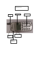
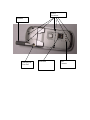
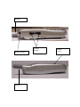
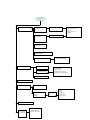
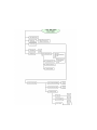
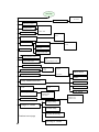
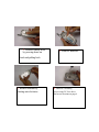
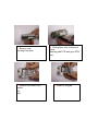
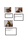
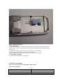
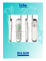
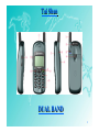
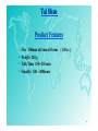
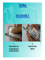
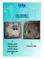
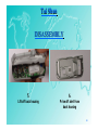
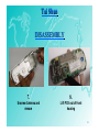
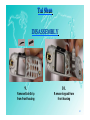
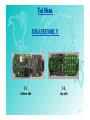
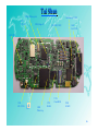
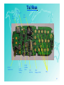
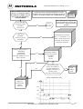
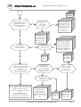
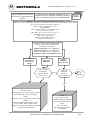
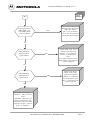
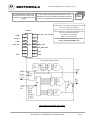
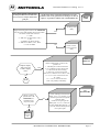
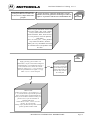
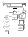
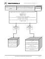
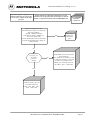
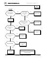
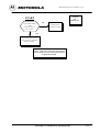
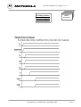
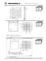
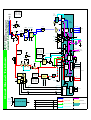
Level 1 and 2
Service Manual
V1.0
CONTENTS
Page Number
SECTION 1: GENERAL
1.1 Introduction
1.2 Motorola service policy for T189 in warranty
1.3 General Safety Information
SECTION 2: T189 DESCRIPTION
2.1 Specifications of T189
2.2 T189 Overview
2.3 Connector Pinout
2.4 Talk time, Weight and Volume Matrix
SECTION 3: FEATURE LIST
3.1 List of Features available
3.2 Phone Book
3.3 Call Related Features
3.4 Messages
3.5 Phone Set Up
3.6 Network selection
3.7 Call Meters
3.9 Accesory Set up
SECTION 4: DISASSEMBLY & PARTS
4.1 Dissasembly Introduction
4.2 Recommended Tools
4.3 Disassembly Procedure
4.4 Assembly procedure
4.5 Exploded Parts diagram
4.6 Replacement parts
SECTION 5: SIM CARDS AND SECURITY
5.1 Manual test mode
5.2 Live Sim Card
5.3 Personality Transfer
5.4 GSM Test Command
5.5 Identity and Security
SECTION 6: REPAIR & TEST PROCEDURES
6.1 Repair introduction
6.2 Mechanical repairs
6.3 Basic modular troubleshooting
6.4 Repair Chart
6.5 Software Upgrade
6.6 Flexing
6.7 Testing on HP8922
SECTION 7: ACCESSORIES
SECTION 8: SALES MODELS
SECTION 9: GLOSSARY OF TERMS
9.1 List of Abbreviations
2.1 Specifications of T189
General
Function
Frequency Range GSM
Frequency Range DCS
Channel Spacing
Channels
Modulation
Transmitter Phase Accuracy
Duplex Spacing
Frequency Stability
Operating Voltage
Transmit Current
Stand-by Current
Dimensions
Size (Volume)
Weight
Temperature Range
Transmitter
Function
RF Power Output
Output Impedance
Spurious Emissions
Receiver
Function
RF Level
RX bit error rate (100 k bits)
Channel Hop Time
Time to Camp
Speech Coding
Function
Speech Coding Type
Bit Rate
Specification
880-915 MHz TX (with EGSM)
925-960 MHz RX (with EGSM)
1710-1785 MHz Tx
1805-1880 MHz Rx
200 kHz
174 GSM/374 DCS carriers with 8 channels per
carrier
GMSK at BT = 0.3
5 Degrees RMS, 20 Degrees peak
45 MHz GSM / 95MHz DCS
+ 0.10 ppm of the downlink frequency (Rx)
Mid RateCharger: = 5.9V, +/-0.3V
Battery Operating Voltage: 2.85V(Radio Shut
Down voltage)
To 4.2V Max)
Typically 290 mA avg,
Typically 10 mA
108mmx43mmx23.5mm (Leap Slim Battery)
85cc
95g with Battery
-10C to +55C
Specification
33 dBm + 2dB GSM/ 30 dBm + 2 dB DCS
50 ohms (nominal)
-36 dBm from 0.1 to 1 Ghz
-30 dBm from 1 to 4 Ghz
Specification
-102 dBm GSM / -100 dBm DCS
< 2%
500 microseconds
Approximately 5-10 seconds
Specification
Regular Pulse Excitation / Linear Predictive Coding
with Long
Term Prediction. (RPE LPC with LTP).
13.0 k bps
Frame Duration
Block Length
Classes
Bit Rate with FEC Encoding
20 ms
260 bits
Class 1 bits = 182 bits. Class 2 bits = 78 bits
22.8 k bps
2.2 T189 Overview
The T189 will incorporate many new features that were, in the past unavailable to the low cost
products. These are:
.Alarm
RTC
Vibrator
Intergrated Headset
96 X 64 Graphics Display with 13 Soft Icons
Single Lion Batteries 580mA
Dual Band GSM 900 and GSM 1800
SIM toolkit V2.2.0
Fig 2.1 Mechanical
pictorial Overview
Antenna
Lens
Vol Up / Down
Speaker
Ports
Headset
Connector
Keypad
Screw
Locations
Antenna
Auxiliary RF
Test Port
SIM Slot
Batt
Contacts
Antenna
Volume
Buttons
Headset Adapter
Antenna
Battery
Cover
2.3 Connector Pinout
2.4 Talk Times, Weight, Dimensions and Volume Matrix
Volume
(cubic
cm)
)
Weight
(grams)
Talk Time
(minutes)
Standby
time
(hours)
Dimensions
(mm)
With
Battery
type:
85
95g
>=150-210
100-200
108mmx43mmx23.5mm
(Leap Slim Battery
580mAh
Lion
Battery
SECTION 3: FEATURE LIST
Personal Numbers
Find Entry
by Name
Enter Name
Find Entry
By Location
Enter Location
1.Call Number
2.Modify Name or
number
3.Erase name and
number
Add Entry
Check Capacity
1.No memory restrictions
2.To SIM card memory
Prevent access
Last Ten Calls
1.Last Calls made
1.Call Number
2.Time and Date
3.Add to Phone memory
4.Add to SIM Card Memory
Last Calls Received
Erase all Numbers
My phone number(s)
Fixed dialing
View fixed dial list
Setup
Fixed
Dialing
Show Services
One-Touch
Dial Setting
1To SIM memory
2 To Fixed Dial list
Enter
Pin2
1.On
2.Off
3.Edit Entry
4.Add Entry
5.Erase Entry
Tower of Hanoi
New Game
Saved Game
Best Score
Bricks
New Game
Saved Game
Best Score
Baccarat
New Game
Saved Game
Best Score
Set Alarm
One Time
Daily
Weekly
Mon-Fri
Mon-Sat
Show Alarm
Disable Alarm
Edit Alarm
Go To Next Alarm
Call Voicemail
Received messages
Go to Next message
Delete Message
Return Call
1.
1.Send Message
2.Store Message
Edit Message
Reply to message
Delete all messages
Go to next message
Outgoing Messages
Send message
Edit message
1.Send message
2.Store message
Delete message
On
Cell broadcast
Off
1.Channel Index
2.Delete all channels
Channel List
Language List
English
Automatic
Message Settings
1.Voicemail Number
2.Service Centre
3.Expiry Period
4.Outgoing message type
Store Message
Message Editor
Edit Message
Send message
1.
Line 1
2. Line 2
Select phone line
Adjust Ring volume
Set Ringer Tone
Standard Tone
:
:
Music Tone
Set Ringer Tone 2
1.On
2.Off
Ringer on or Off
Phone Lock
1.On
2.Off
Automatic Lock
Lock Now
Adjust Contrast
Change Unlock mode
Change SIM PIN2 Code
Require SIM card pin
1.On
2.Off
3.Change SIM pin Code
New security code
Extended menus
1.On
2.Off
English
:
:
:
Automatic
Language Selection
BoPo MoFo
Stoke
Entry Method Selection
Battery saving
mode
Select Keypad tones
Pin-Yin
1.On
2.Off
1.Normal Tones
2.Single Tones
3.No Tones
Phone Status
Ringer Only
Ringer or Vibrate
Vibrate Only
Vibrate then Ring
Continue to next page
No Ring Or Vibrate
iTAP
TAP Mode
1.Status review
2.Master reset
3.Master Clear
Continue from previous page
Set Alarm Ringer Tone
1.On
2.Off
Standard Tone
:
:
Music Tone
Set Message Alarm Tone
Set Time and Date
Set Time
Set Date
Show Time And Date
24h
Set Time Format
12h
SECTION 4: DISASSEMBLY
&PARTS
4.1 Disassembly Introduction
The T189 is held together by 6 screws, 2 uppermost and 4 within the battery casing. Ensure care is
taken when removing the LCD from the main PCB as the flex is very delicate and can be easily
damaged.
Ensure that a properly grounded high impedance conductive wrist strap is used whilst performing any
tasks during the disassembly and assembly of the unit
Avoid stressing the plastics in any way to avoid damage to either the plastics or internal components.
Many of the intergrated devices used in this equipment are vulnerable to damage from
electro-static charges. Ensure that adequate static protection is in place when handling,
shipping and servicing the internal components of this equipment.
!!
4.2 Recommended Tools
The following tools are recommended for use during the assembly / disassembly of the T189.
• Anti-static Mat Kit - 0180386A82, includes:
Antistatic mat 66-80387A95
Ground Cord 66-80334B36
Wrist Band 42-80385A59
• Plastic Bladed Tool SLN7223A
• T6 Torx Driver
4.3 Disassembly Procedure
The following set of diagrams will demonstrate the correct sequence and action required to disassemble
the T189
.
4.4 Assembly Procedure
Once the unit is disassembled and the repair is carried out, the unit must then be reassembled, this is
carried out in the exact reverse order as the disassembly.
!! CAUTION !!
Many of the intergrated devices used in this equipment are vulnerable to damage from
electro-static charges. Ensure that adequate static protection is in place when handling,
shipping and servicing the internal components of this equipment.
1. Remove battery door
by pressing down on
2. Remove Batteries
latch and pulling back
3. Remove antenna by
4. Unscrew 6 retaining
rotating anti-clockwise
screws using T6 Torx driver
find screw locations on page 4
5. Remove rear
housing from unit.
7. Remove the rubber side
panels
the
unit.
6. Slide plastic tool in between
front
housing and PCB and prise PCB
out.
8. Remove Keypad
9. Remove alert speaker
from front housing
11. Carefully lift the flip of
the ZIF connector and
remove the flex Note: The
flex is very fragile.
10. Carefully prise display
LCD
from main board by releasing
catches on each side of LCD
frame
4.5 Exploded Parts Diagram
1
2
4
3
5
6
8
7
9
10
12
11
13
15
14
4.5Replacement Parts
1
TBD
2
3
4
5
6
7
8
9
10
11
12
13
14
15
Front Housing
Rear Housing
Battery cover
Vibrator
Antenna
Number Keypad
Mylar Dome
LCD ASSY
LCD Lens
Mic & Grommet
Speaker earpiece
Side Key
Power Key
Screw
SECTION 5: SIM CARDS AND
SECURITY
5.1 Manual Test Mode
The GSM Motorola T189 is equipped with a manual test mode capability. This capability allows
service personnel to take control of the unit, and by entering certain keypad commands, make the unit
performs desired functions.
To enter the manual test command mode, a GSM / DCS mini test sim (Part No 8102430Z04) must be
used.
The test sim is inserted into the SIM slot in the side of the phone (See figure 6.1), the battery should
then be inserted and the unit powered on. The # button should then be pressed for approximately 3
second until ‘test’ appears on the display, and the correct commands must then be followed.
Figure 6.1 SIM Card insertion
5.2 Live Sim Card
A SIM (Subscriber Identity module) card will be required to access the existing local GSM / DCS
cellular network, or remote networks when travelling. (If the roaming agreement has been made with
the provider.)
The SIM card contains all the data necessary to access GSM services, and also:
• The ability to store user information such as phone numbers etc…
• All information required by the network provider to provide use to the network
5.3 Personality Transfer
No personality transfer available on this product.
5.4 GSM Test Commands
This is a list of Level 1 and 2 Test commands available to T189
Table 5.1 Test commands
Key Sequence
#(hold down for 2 seconds)
01#
07x#
Test Function/Name
Enter manual test mode
Exit manual test mode
Mute RX audio path
08#
09#
10#
15x#
16#
19#
20#
36#
37#
38#
39#
43x#
51#
52#
54X#
Unmute RX audio path
Mute TX audio path
Unmute TX audio path
Generate tone
Mute tone generator
Display S/W version number of Call Processor
Display S/W version number of Modem
Initiate acoustic loopback
Stop test
Activate Mini SIM
Deactivate Mini SIM
Change audio path
Enable sidetone
Disable sidetone
Show Service Indicator LED 0 - Off / 1 – Red / 2 –
Green / 3 – Amber
(Flip must be Closed)
Initialize non-volatile memory
Display security code
Modify security code
Display lock code
Modify lock code
Display IMEI
DCS / GSM mode
Display all display pixels
57#
58#
58xxxxxx#
59#
59xxx#
60#
980# / 981#
99#
15XX#
91
Constant Ringer
36XX#
0 or Omitted
1
2
Full Rate
Enhanced Full rate
Half Rate
5.5 Identity and Security
Each Motorola T189 will be labelled with various number configurations. The following information
describes what these configurations mean.
MSN
The mechanical Serial Number (MSN) is an individual unit identity number and will remain with the
unit throughout the life of the unit.
The MSN can be used to log and track a unit on Motorola’s EPPRS system.
The MSN is divided into 4 sections.
IMEI
The International Mobile station Equipment Identity (IMEI) number is an individual number unique to
the PCB and is stored within the unit’s memory. The following figure gives a description of the make
up of this number.
Some other label number configurations that will be present will be: -XCVR
NUMBER: Identifies type of product. i.e. T189 (Usually SWF number)
PACKAGE NUMBER: Determines type of equipment, mode in which it was shipped and language
with which it was shipped.
SECTION 6: REPAIR AND TEST
PROCEDURES
6.1 Repair Introduction
The T189 is divided into 3 main sections when it comes to part replacability: The Flip which contains
the speaker,battery connections, RTC battery and Vibrator. The housings that contain the main PCB
which contains RF / Logic circuitry. The third component is the the keypad and Display Assy. If the
RF / Logic board is required to be changed then a full service tranceiver should be ordered as there is
no replacement PCB available. Also a personality transfer would be necessary.
6.2 Mechanical repairs
Assembly replacement level troubleshooting and repair of the T189 is limited to isolation and
replacement of the main mechanical parts only (See Exploded parts diagram and associated parts list)
6.3 Basic Modular Troubleshooting
The troubleshooting information in Table 2 shows some typical malfunction symptoms, and for the
corresponding verification and repair procedures refer to the disassembly instructions located in the
disassembly section of this manual. (Section 5).
NOTE Defective Logic/RF assemblies must be replaced
with pre-tested, pre-phased assemblies
6.4 Repair Chart
Table 2. GSM T189 Cellular Telephone: Troubleshooting and Repair Chart. (Assembly Replacement
Level).
SYMPTOM
Personal telephone will not turn on or
stay on
PROBABLE CAUSE
a)
Battery pack either
discharged
or defective
Battery connectors open
or
misaligned.
VERIFICATION AND
REMEDY
Replace batteries with known good cells.
Power unit
on. If unit powers on OK replace batteries.
If battery is not at fault, proceed to b.
b)
c)
Logic/RF Board
Assembly
Defective.
d) Display circuit failure
2. Personal telephone exhibits poor
reception and/or erratic operation (such
as calls frequently dropping, weak
and/or distorted audio, etc.).
a) Antenna is defective
b) Logic/RF Board Assembly
Defective.
3. Display is erratic, or provides
Partial or no display.
a)
Mating connections to /
from
Display PCB.
b)
Display Module is
Defective.
Visually inspect the battery connectors on
the rear
housing top and bottom. Check for bad
alignment or
dirty contacts. Re-align, clean and, if
necessary,
replace the rear housing. If battery
connectors are not
at fault, proceed to c
Remove the Logic/RF Assembly.
Substitute a known
good assembly and temporarily
reassemble the unit.
Depress the PWR button; if unit turns on
and stays
on, disconnect the dc power source and
reassemble
the telephone with the new Logic/RF
Board
assembly. If unit does not power up
proceed to d)
Disassemble unit and remove LCD
module and
insert known good module. Insert Battery
and
depress PWR button. Ensure unit stays
on, if OK
reassemble unit in new housing assembly
Check to make sure that the antenna is
properly
inserted into the front housing. If OK,
substitute a
known good antenna. If the fault is still
present,
proceed to b.
Replace Logic/RF Assembly (refer to
symptom 1c).
Verify that the fault has been cleared and
Re-assemble the unit with the new PCB.
Dissasemble unit, and remove display
module from
main PCB, check connector for any signs
of
corrosion or damage. If damaged proceed
to c)
Substitute a known good Display Module
onto the
suspect main board and connect to DC
Pwr supply
depress PWR and ensure display is now
c)
Defective.
Logic/RF Board
Assembly
correct, If
Ok rebuild unit with new Display
assembly. If
display assembly is not at fault proceed to
c.
Replace Logic/RF Assembly (refer to
symptom 1c).
Verify that the fault has been cleared and
Re-assemble the unit with the new PCB.
SYMPTOM
4. Incoming call alert transducer
audio, distorted or volume is too
low.
PROBABLE CAUSE
a) Faulty alert Transducer
b)Main RF / Logic PCB
defective
5. Personal telephone transmit audio
is weak, (usually indicated by called
parties complaining of difficulty in
hearing voice from personal phone).
a)
Microphone connections
to
the main RF / Logic board are
defective.
b) Microphone defective
b)
Logic/RF Board
Assembly
defective.
6. Personal telephone receive audio
is weak and/or distorted. (From
speaker)
Dirty Contacts / Misalignment
of contacts or faulty speaker.
c)
Antenna assembly is
defective.
d)
Defective.
Logic/RF Board
Assembly
VERIFICATION AND REMEDY
Replace Alert Transducer from rear
housing refer to
disassembly procedure.If not Alert then
proceed to b)
Replace Logic/RF Board Assembly (refer
to
symptom 1c). Verify that the fault has
been cleared
and re-assemble the unit with the new
PCB.
Gain access to the Microphone as
described in the
DISASSEMBLY instructions in this
manual. . Check
connections. If connector is faulty proceed
to c if the
connector is OK, proceed to b.
Gain access to microphone .Disconnect
and
substitute a known good Microphone.
Place a call
and verify as heard by called party. If
good, re-assemble
unit with new Microphone. If Microphone
is not at fault, re-install original
Microphone and
proceed to c.
Replace Logic/RF Board Assembly (refer
to
symptom 1c). Verify that the fault has
been cleared
and re-assemble the unit with the new
PCB.
Ensure pads on PCB are clean and that
speaker
contacs are sat almost vertical to each
other. If Ok
replace with known good speaker and
check for call
quality. If still poor proceed to c)
Attempt a re-phasing of the unit and
recheck the
symptom. If symptom is the same but unit
re-phases
correctly, check to make sure the antenna
connector
is correctly soldered to the main board and
that the
antenna is fitted correctly. If ok, substitute
a known
good antenna assembly. If this does not
cure the
fault, re-install the original antenna then
proceed to
d).
d) Replace Logic/RF Assembly (refer to
symptom
1c). Verify that the fault has been cleared
and Re-assemble
the unit with the new PCB.
7. Personal telephone will not
recognize/accept SIM card
a) SIM card defective
Initially check that the contacts on the
card are not
dirty. Clean if necessary, and check if
fault has been
eliminated. If the contacts are clean, insert
a Known
good SIM card into the unit. Power up the
unit and
confirm whether or not the card has been
accepted. If
the fault no longer exists, the defective
SIM card
should be replaced. If the SIM card is not
at fault,
proceed to b.
d)
Logic/RF Board
Assembly
Defective.
SYMPTOM
9. Internal Charger not working
PROBABLE CAUSE
a) Batteries faulty
Faulty charger circuit on
main
board defective
Replace Logic/RF Board Assembly (refer
to
symptom 1c). Verify that the fault has
been cleared
and re-assemble the unit with the new
PCB.
VERIFICATION AND REMEDY
Replace suspect batteries with known
good items.
Insert charger and ensure battrey charging
icon
flashes if OK, replace batteries if batteries
still do not
charge proceed to b)
a)
10. No / Weak audio when using
a) Headset not fully pushed
headset
home
still no audio proceed to b)
b)
Faulty Jack Socket /
Defective PCB
6.5 Software Upgrade
Replace Logic/RF Board Assembly (refer
to
symptom 1c). Verify that the fault has
been cleared
and re-assemble the unit with the new
PCB.
Fully ensure the ‘click’ is felt on the jack
socket. If
Replace Logic/RF Board Assembly (refer
to
symptom 1c). Verify that the fault has
been cleared
and re-assemble the unit with the new
PCB.
For information on setting up and equipment required for the flashing of software, contact should be
made with the local technical support engineer.
6.6 Flexing
For information on setting up and equipment for flexing, contact should be made with the local
technical support engineer.
6.7 Testing on HP8922
SECTION 7: ACCESSORIES
(TBD)
SECTION 8: SALES MODELS
(TBD)
SECTION 9: GLOSSARY OF
TERMS
9.1 List of Abbreviations
Those marked ** are Motorola specific abbreviations.
A Interface Interface between MSC and BSS
A3 Authentication algorithm
A5 Stream cipher algorithm
A8 ciphering key generating algorithm
AB Access Burst
A-bis Interface between BSC and BTS
ACCH Associated Control Channel
ACSE Association Control Service Element
AGCH Access Grant Channel
AMPS Advance Mobile Phone System
AOC Advice of charge
ARFCN Absolute Radio Frequency Channel Number
ARQ Automatic Request for retransmission
ASIC Application Specific Integrated Circuit
AUC Authentication Center
AUT (H) Authentication
BA BCCH Allocation
BAIC Barring of All Incoming Calls
BAOC barring of all Outgoing Calls
BCC Base Transceiver Station (BTS) Color Code
BCCH Broadcast Control Channel
BCD Binary Coded Decimal
BCU BTS Control Unit **
Bm Full-rate traffic channel
BN Bit Number
BS Base Station
BSC Base Station Controller
BSIC Base Transceiver Station Identity Code
BSS Base Station System
BSSAP BSS Application Part (DTAP and BSSMAP)
BSSC Base Station System Control Cabinet **
BSSMAP Base Station Systems Management Application Part
BSSOMAP BSS Operation and Maintenance Application Part
BSU Base Site Controller Unit **
BTS Base Transceiver Station
CA Call Allocation
CBCH Call Broadcast Channel
cc Call Control
cc Country Code
CC Cellular Cassette
CCBS Completion of Calls to Busy Subscribers
CCH Control Channel
CCCH Common Control Channel
CDMA Code Division Multiple Access
CFS Call Forwarding on mobile Subscriber busy
CFU Call Forwarding Unconditional
CLIP Calling Line Identification Presentation
CLIR Calling Line Identification Restriction
CM Connection Management
COLP Connected Line identification Presentation
COLR Connected Line identification Restriction
CONF Conference Call add on
CSPDN Circuit Switched Public Data Network
CUG Closed User Group
CW Call Waiting
DB Dummy Burst
DBS Distributed Base Station **
DCCH Dedicated Control Channel
DET Detach
DFE Decision Feedback Equalizer
DISC Disconnect
DL Data Link (layer)
Dm Control Channel (ISDN terminology applied to mobile service)
Dm Signaling channel
Dp Dialed Pulse
DRCU Diversity Radio Channel Unit**
DRX Discontinuous Reception
DTAP Direct Transfer Application Part
DTE Data Terminal Equipment
DTMF Dual Tone Multi-Frequency (tone signaling type)
DTX Discontinuous Transmission
E erlang
Eb/No Energy per Bit/Noise floor
EC Echo Canceller
Ec/No Ratio of energy per modulating bit to the noise spectral density
EGSM Extended Group special Mobile
EFR Enhanced Full Rate
EIR Equipment Identity Register
EIRP Effective Isotropic Radiated Power
EMC Electromagnetic Compatibility
EMX Electronic Mobile Exchange **
ETSI European Telecommunications Standards Institute
FACCH Fast Associated Control channel
FACCH/F Full rate Fast Associated Control channel
FACCH/H Half rate fast Associated Control channel
FB Frequency correction burst
FCCH Frequency Correction Channel
FEC Forward Error Correction
FN Frame Number
FR Full Rate
FTAM File Transfer Access Management
GCC Global Call Center
GMSC Gateway Mobile Services Switching Center
GMSK Gaussian Minimum Shift Keying
GSM Group Special Mobile
GSM MS GSM Mobile Station
GSM PLMN GSM Public Land Mobile Network
HANDO Handover
HDLC High Level Data Link Control
HLR Home Location Register
HOLD Call Hold (Supplementary Service)
HPLMN Home PLMN
HPU Hand Portable Unit
HR Half Rate
HSN Hopping Sequence Number
I Information (frames)
IA5 International Alphanumeric 5
ID Identification
IMEI International Mobile Equipment Identity
IMM Immediate assignment message
IMSI International Mobile Subscriber Identity
IN Intelligent Network
INDY Iridium 9500 handset
ISC International Switching Center
ISU Iridium Subscriber Unit
ISDN Integrated Services Digital Network
ISUP ISDN User Part
IWF Interworking Function
Kc ciphering Key
Ki Individual subscriber authentication key
LAC Location Area Code
LAI Location Area Identification (Identity)
LAPB Link Access Procedure ‘B’ (balanced) channel
LAPDm Link Access Procedure ‘DM’ (mobile ‘D’) channel
Lm Traffic channel (with capacity lower than Bm)
LPC Linear Predictive Code
LR Location Register
MA Mobile Allocation
MAH Mobile Access Hunting
MAI Mobile Allocation Index
MAIO Mobile Allocation Index Offset
MAP Mobile Application Part
MCC Mobile Country Code
MCI Malicious Call Identification
MD Mediation Device
ME Mobile Equipment
MF Multi-Frequency (tone signaling type)
MLSE Maximum Likelihood Sequence Estimator
MM Mobility Management
MMI Man Machine Interface
MNC Mobile Network Code
MO Mobile Originated
MO/PP Mobile Originated Point to Point messages
MoU Memorandum of Understanding
MRN Mobile Roaming Number
MS Mobile Station
MSC Mobile Services Switching Center
MSCM Mobile Station Class Mark
MSIN Mobile Station Identification Number
MSISDN Mobile Station international ISDN number
MSRN Mobile Station Roaming Number
MT Mobile Termination
MTP Message Transfer Part
MT/PP Mobile Terminated Point to Point messages
NAMPS North American-Advance Mobile Phone System
NB Normal Burst
NE Network Elements
NET Norme European de Telecommunications
NM Network Management
NHC Network Management Center
O&M Operations and Maintenance
OACSU Off Air Call Set-Up
OCB Outgoing Calls Barred
OMAP Operations and Maintenance Application Part (previously was OAMP)
OMC Operations and Maintenance Center
OMCR Operations and Maintenance Center -Radio Part
OMCS Operations and Maintenance Center -Switch Part
OTA Over The Air Programming
OSI Open System Interconnection
PAD Packet Assembly Disassembly facility
PCH Paging Channel
PDN Public Data Networks
PIN Personal Identification Number
PLMN Public Land Mobile Network
POTS Plain Old Telephone Service (basic telephone services)
PSPDN Public Switched Packet Data Network
PSTN Public Switched Telephone
PTO Public Telecommunications Operator
QOS Quality of Service
RAB Random Access Burst
RACH Random Access Channel
RBDS Remote BSS Diagnostic Subsystem **
RBU Remote Base Station Unit (PCN) **
RCU Radio Channel Unit **
REC Recommendation
REL Release
RELP-LTP Regular Pulse Excitation - Long Term Prediction
REQ Request
RFCH Radio Frequency Channel
RFN Reduced TDMA Frame Number
RLP Radio Link Protocol
ROSE Remote Operations Service Element (a CCITT specification for O&M)
RXCDR Remote Transcoder Unit **
RXLEV Received signal level
RXQUAL Received signal quality
SABM Set Asynchronous Balance Model
SACCH Slow Associated Control Channel
SAPI Service Access Point Indicator (Identifier)
SB Synchronization Burst
SC Service Center
SCCP Signaling Connection Control Part
SCH Synchronization Channel
SCP Service Control Point - an intelligent network entity
SDCCH Stand-alone Dedicated Control Channel
SDL Specification Description Language
SFH Slow Frequency Hopping
SIM Subscriber Identity Module
SMS Short Message Service
SMSCB Short Message Service Call Broadcast
SND SeND
SP Signaling Point
SRES Signed RESponse (authentication)
SS Supplementary Service
SS System Simulator
STP Signaling Transfer Point
SYSGEN SYStem GENeration
TA Terminal Adapter
TA Timing Advance
TCAP Transaction Capabilities Application Part
TCH Traffic Channel
TCH/F A full rate TCH
TCH/FS A full rate speech TCH
TCH/HS A half rate speech TCH
TCP Transmission Control Protocol
TDMA Time Division Multiple Access
TE Terminal Equipment
TMN Telecommunications Management Network
TMSI Temporary Mobile Subscriber Identity
TN Timeslot Number
TRX Transceivers
TTY TeleTYpe (refers to any terminal)
TS Time Slot
TUP Telephone Users Part
UI Unnumbered Information frame
Um Air Interface
VAD Voice Activity Detection
VLR Visited Location Register
VLSI Very Large Scale Integration (IC)
VPLMN Visited PLMN
XC Transcoder
XCDR Transcoder **
3PTY Three party service
Tai Shan
DUAL BAND
1
Tai Shan
DUAL BAND
2
Tai Shan
Product Features
*Platform
*Dual
*Full
multiple forms/looks
band CSM900/1800
matrix 96x64 graphics display with 13 soft icons
*Integrated
headset jack
*Side
Mounted Volume Switches
*SIM
toolkit
*Microbrowser
(UP 3.1 ) Capable
3
Tai Shan
Product Features
*
*
*
*
Size 108mm x42 mm x18 mm ( 120 cc )
Weight 120 g
Talk Time 150--210 min
Standby 100 --200hours
4
Tai Shan
Design Approach
*
*
*
*
*
*
*
*
3.6 V Platform
3.6 V LDMOS PA Application
VCO Modules
Front End IC
No Accessory Connector
Stacked Flash Memory/SRAM
Individual Battery Cells vs.. Battery Pack
Leap charge circuit
5
Tai Shan
The main updates based on shark
Phone Book: 100 phone memory, SIM card memory (20+)
Leap charging circuitry and software.
Clock/Alarm with battery backup.
Vibrator.
MMI refreshment
Butt-plug circuitry migration from Leap
WAP removed
6
Tai Shan
The main updates based on shark
WAP removed
Games
Calculator (To be confirmed)
Edit / Send Ringer Tone via SMS
SMS with CLI
No personalized banners
No quick access key (cd928 type keyboard)
7
Tai Shan
DISASSEMBLY
1.
Remove battery door
by pressing down on
clip and pulling back
2.
Remove the three
batteries
8
Tai Shan
DISASSEMBLY
3.
Press down and pull
SIM card lid to right
and lift. For removing
pull horizontally to the
left.
4.
Unscrew all 6 screws
9
Tai Shan
DISASSEMBLY
5.
6.
Lift off back housing
Prise off alert from
back housing
10
Tai Shan
DISASSEMBLY
7.
8.
Unscrew Antenna and
remove
Lift PCB out of front
housing
11
Tai Shan
DISASSEMBLY
9.
10.
Remove Side Grip
from front housing
Remove keypad from
front housing
12
Tai Shan
DISASSEMBLY
11.
Unclip display board latches at both sides of PCB and detach carefully
13
Tai Shan
DISASSEMBLY
12.
Lift hinge from ZIF connector and remove carefully flex-print
14
Tai Shan
DISASSEMBLY
13.
bottom side
14.
top side
15
Tai Shan
Y200, 26Mhz crystal
U301
TX VCO
J604 Battery CONN
l
U200, Magic IC
J803 SIN CONN
J600
Ext CONN
Q370 TPA
J300
RF CONN
U350
PAC
U800
White Cap
U702
SRAM
U701
Flash ROM
U900
GCAPE
16
Tai Shan
U432
Front end IC
J510
Buzzer
FL472
Filter
J50504
Headset Jack
U905
Back up
battery
FL490
400Mhz
Filter
U253
3U253
RX VCO
J902
Display CONN
LED
LED
17
Taishan level 3 debug
issue30/11/2000
Dual Band Taishan
Dual band level 3 debug
Version: 1.0
Prepared by
Tony Zhang
Date: Nov , 30 , 2000
Approved by _____________________
Total Pages: 19
- MOTOROLA INTERNAL USE ONLY -
Shark level 3 debug
issue31/11/2000
REVISION HISTORY
Version
Date
Name
Reason
1.0
23/12/1999
Fabrizio Alba
First release
- MOTOROLA INTERNAL USE ONLY -
Dual band Taishan level 3 debug rev 1.0
lunedµ 20 dicembre 1999
Supply phone by Buttplug
Leap Slim Li-ion battery
code SNN5520A and check following
tests sequence
Does phone
power up
correctly ?
For any page see
electrical
diagram
equivalent
NO
Taishan
test sequence
Go to " no
power up "
on pag. 03
YES
Does phone
draw a lot of
current ?
YES
ON
FUTURE
NO
Does display
works
correctly?
NO
Go to " no
display " on
pag.11
YES
Does
backlight
works
correctly?
NO
Go to " no
backlight "on
pag.11
NO
Go to " no
keypad " on
pag.12
YES
Does keypad
works
correctly?
YES
Does phone
shows "phone
failure see
supplier ?
YES
ON FUTURE
NO
go to " 1 "
PAG 02
- MOTOROLA CONFIDENTIAL PROPRIETARY -
Page 1
Dual band Taishan level 3 debug rev 1.0
lunedµ 20 dicembre 1999
"1"
Taishan
test sequence
Connect phone to HP 8922 (active
cell)
Does phone go into service
at -102dBm in GSM/DCS
mode?
NO
Go to " no rx
GSM/DCS "
on pag.05
NO
Go to " no tx
GSM / DCS "
on pag.07
YES
Does phone initiate a call on
GSM/DCS mode?
YES
Make a phone call from analyzer
Is ringer tone audible ?
NO
YES
Go to " no
alert " on
pag.12
Answer call
Is audio tx working
correctly?
NO
Go to " no
microphone "
on pag.14
YES
Is audio RX on speaker
working correctly?
NO
YES
Go to " no
audio on
speaker " on
pag.13
Insert headset on properly connector
Are audio TX & RX
working correctly on
headset?
NO
Go to " no
TX/RX audio
on headset "
on pag.14/15
YES
Does internal charger and
vibrator work correctly ?
NO
Go to No charger page 16
no vibrator page 17
YES
Not fault
found
- MOTOROLA CONFIDENTIAL PROPRIETARY -
Page 2
Dual band Taishan level 3 debug rev 1.0
lunedµ 20 dicembre 1999
note: all the signal & voltage present
in this procedure has to be clear and
at correct level ; compare them with a
good pcb
NOTE: check if any components mentioned is correctly
positioned , has not dry joint and is not damaged . If all is ok
replace it . If problem is still the same send BOARD IN htc.
NO
POWER
UP
Supply phone using
Ext_B+ (~4.5V) on Butt-plug
YES
and check if
phone power up correctly
NO
set power supply
generator to 4 Vcc and
check if phone power up
correctly
YES
Check Ext_B+ from J600
to CR903 if OK
Check CR903, Q905
and NOTE1 or faulty.
NO
Make a short on W.D. line on R941 side ( near
C913 ) AND CHECK FOLLOWING
FOLTAGES:
-V_BOOST = 5,6 V on C913
-V1 =5V on C906
-V2 =2,8 V on C939
(R905)-V3 = 1,8 V on C909
-SR_VCC = 2,8 V on R722
-VRef =2,8 V on C919
SEE TIMING SEQUENCE on Pag. 16 , 17.
NO
For V_BOOST issue check L901 ,
C980 , C970 , C981 , CR 902 ,
C913 for other voltages issues
check any line for short or different
resistence ( compare with a good
one ).
YES
Does 26 MHz
clock is
present on
L220 ?
YES
Go to " 2 "
on pag. 03
NO
Check Y200 , C220 , L220 for
missing , dry joint or faulty , check
also for " VRef " voltage presence
= 2,8 V on C213 , if not ok check
line between C919 & C213.
Finally check on C215 for "RF_V2
" voltage = 2,8 V presence and for
" RF_V1 "voltage = 2,8 V on
C217.
- MOTOROLA CONFIDENTIAL PROPRIETARY -
Page 3
Dual band Taishan level 3 debug rev 1.0
lunedµ 20 dicembre 1999
NO
POWER
UP
"2"
Does " MAGIC 13
MHz " clock is
present on TP 200
or C817 ?
Check for 13 MHz frequency
presence on CR248 , if not ok
check any components surround
it for missing , dry joint or faulty
; check also V1_SW = 5 V
presence on R234 ( it comes
from Q913 ) .
If all is ok probably U200 faulty.
NO
YES
Does "
GCAP_CLK
13MHz " is
present on TP
823 or C825 ?
Check following voltages before
replacing U800:
2,8V=VDSS on R813
2,8V= VCC_MEMIF on R819
2V=VDD on R823
2V = VCCA on R825
NO
YES
Is reset voltage
at 2,7 V present
on C820 ?
NO
REPLACE
U900
YES
Is CE0 ,flash ic chip
enable present on TP
824 ?
NO
Check for V2 =
2,8 V presence on
C700 , C703 ,if
they are ok replace
U701
YES
Is CE2 , ram ic
chip select
present on TP
825 and CE3 on
TP 826 ?
NO
YES
Check for U702
power supplies
SR_VCC on C701 ,
R722, if not ok
replace U900 , else
replace U701.
HTC
- MOTOROLA CONFIDENTIAL PROPRIETARY -
Page 4
Dual band Taishan level 3 debug rev 1.0
lunedµ 20 dicembre 1999
Connect on J300 connector an RF
generator , set frequency equal to
947,4 MHz level -30dBm . Set pcb
in test mode and digit RX test
command 450062#
Is IF at 400 MHz
frequency present
on C498 at
correct level ?
NOTE: check if any components mentioned is correctly
positioned , has not dry joint and is not damaged . If all is ok
replace it . If problem is still the same send BOARD IN htc.
note: all the signal & voltage present
in this procedure has to be clear and
at correct level ; compare them with a
good pcb
Go to "
A " on
pag .06
NO
NO RX
GSM/DCS
YES
Is RX_LO at
800 MHz
frequency present
on CR249 ?
NO
Check Q203 for correct bias
:base = 1,7 V;collector= 2,7 V;
emitter = GND .check also for
any faulty on CR 249 and
components surround it
YES
Check for data presence on:
- R299 BDR
- R299 BFSR
- R287 BCLKR
Note: digit 450062# for every
point of measure
NO
NO
YES
NO
With PCB in stand by
check for data presence
on SPI BUS:
TP 205
TP 206
YES
Does RX ACQ signal
works correct whenever
you digit 450062# test
command , check this on
TP "RX_ACQ"?
See receiver timing below
YES
Check
U200 for
faulty
Problem could be
U800,try to
resolder it,after
replace
component.
- MOTOROLA CONFIDENTIAL PROPRIETARY -
Page 5
Dual band Taishan level 3 debug rev 1.0
lunedµ 20 dicembre 1999
A
NO RX
GSM/DCS
Have you same issue also
using DCS RX WAY ? set
RF generator at 1842,8
MHz and digit 450700#
test command.
NO
Is RF signal (digit
450062# ) at
947,4 MHz
present on FL 472
pin 2?
YES
NO
Check C472 , C473 ,
L471 for missing or
dry joint ,else check
C484 , C486 , L485 ,
L482 , R481. If all is
ok replace U432
YES
Is IF 400 MHz
frequency present on
U432 pin 3 & 4 ?
YES
Is IF 400 MHz
frequency present
on FL 490 pin 5?
Check RF at GSM freq.
presence on FL 472 IN, if
it is ok replace FL 472 ,
else problem is FL 470 (
true only if you are sure
that on DCS way
everything is ok ).
Check Q490 for correct bias
: base = 0,8 V ; collector =
1,6 v ; emitter = GND .
SW_VCC comes from
YES
U200 , else check any
components surround it for
faulty or missing
NO
REPLACE FL
472 (GSM )
FL 480 (DCS)
REPLACE
FL490
YES
Is RF RX signal present on:
U432 pin 18 AT 947,8 MHz
frequency (GSM way digit
450062#)
U432 pin 12 at 1842,8 MHz
( DCS way digit 450700#)?
NO
NO
Is RF signal ( as
before) present on
FL472 in using GSM
way or on FL 480 IN
using DCS way way ?
YES
Is there same signal
on FL 472 ( GSM
WAY )
FL 480 ( DCS WAY )
NO
Is there RF signal
on C470 for GSM
&DCS way?
YES
YES
YES
NO
Check on U432 pin 7 for RX VCO presence
at 1347,4 MHz for GSM or at 1442,8 MHz
for DCS ,if ok check U432 for
correctbias,else check U253 for faulty.
Note:
RX_VCO250 see on Q172
RX_DCS*GSM see on Q160
V_tuning,on pin 1, see R221,U200.
SEE U432 DIAGRAM ON PAG.18
Check for faulty:
J300,U100,Q110.
TX_EN comes from
U800,RX_EN comes from
U800 , -5Vcc comes from
U903
REPLACE
FL470
- MOTOROLA CONFIDENTIAL PROPRIETARY -
Check for GSM
C472,C473,L471.
for DCS C482 ,
C483 , L481
Page 6
Dual band Taishan level 3 debug rev 1.0
lunedµ 20 dicembre 1999
note: all the signal & voltage present
in this procedure has to be clear and
at correct level ; compare them with a
good pcb
NOTE: check if any components mentioned is correctly
positioned , has not dry joint and is not damaged . If all is ok
replace it . If problem is still the same send BOARD IN htc.
NO TX
GSM/DCS
NOTE 1 : You can use this procedure for GSM way & DCS way.
Whenever you have a signal with a simbol star ( * ) means that it is active low if you select this kind of way , while
the same point of measure will be high for other way.
Differences betwen GSM & DCS way are:
TX_GSM*DCS
used for adjust all RF TX way for GSM/DCS choise
for any problem check on Q160
DCS_SEL comes out from U200 (or pin 2 U110)
GSM_SEL comes out from U110 pin 4
-10 V comes out from U904.
DCS_TX_VCO , GSM_TX_VCO
for any problem check Q130
Connect on J300 connector an RF spectrum
analyzer , set pcb in test mode and digit
following test command:
110062# 1215# 40# for a test in GSM way.
110700# 1215# 40# for a test in DCS way.
Check for RF signal presence at frequency =
902.4 MHz for GSM or 1747.8 MHz for DCS .
RF IS PRESENT ,
NEVER MIND
LEVEL BUT IS
DIRTY
RF IS
PRESENT
BUT IS LOW
RF IS NOT
PRESENT
Is RF TX signal
at GSM/DCS
frequency present
on U301 pin 4 ?
YES
Is RF TX
GSM/DCS
present on
Q370 DRAIN?
NO
Go to "
B " on
pag.08
NO
YES
Check on U301:
pin 3 DCS_TX_VCO see on Q130 , Q140.
pin 8 GSM_TX_VCO see on Q130 ,
Q140.
pin 10 SF_OUT see on C246 ( comes from
U200 9.
pin6 CP TX check for this Q310 , Q311 ,
U310 , U200 , R305 , R306 , R307.
DM_CS , TX_EN , they comes from U800
V1_SW comes from Q913
Check:
L365 , L325 , L326 ,
C397for missing or dry joint
, else check for faulty Q110 ,
U100.
-5V cc see U903
TX_EN , RX_EN comes
from U800
- MOTOROLA CONFIDENTIAL PROPRIETARY -
Page 7
Dual band Taishan level 3 debug rev 1.0
lunedµ 20 dicembre 1999
NO TX
GSM/DCS
"B"
Is RF signal at 902,4
MHz ( GSM ) or at
1747,8 MHz ( DCS )
on Q331 collector
YES
Check Q370 for correct bias:
drain = B+ voltages
gate = 1,3 V see for this
L370 , L336 , R370 presence
,else PAC IC bias on pag.09
NO
Is RF GSM/DCS
signal present on
Q330 collector
YES
Check R304 , L331 , C315
, and Q331 for correct bias:
REG B+ = 3,3 V voltage on
collector ,see for this Q332 ,
Q333.
0,4 V on base see for this L333 ,
R302 , CR330 , R387,else PAC
IC bias on page 09
NO
Is RF GSM/DCS
signal present on
Q320 collector
YES
Check C1619 , R301 ,
CR320 , L320 , C326 ,
Q330 for correct bias:
collector = 3,3 V REG B+
,see for this Q332 , Q333;
base = 1 V see R330 , PAC
IC bias on pag. 09.
NO
Check Q320 for correct bias :
collector = 2 V RF_V2 see on
L322
, R300 base = DM_CS se on
R326 , it comes from U 800
else be sure to have correct RF
signal on U301 pin 1 ,if not ok
go to " C " on page 07.
- MOTOROLA CONFIDENTIAL PROPRIETARY -
Page 8
Dual band Taishan level 3 debug rev 1.0
lunedµ 20 dicembre 1999
note: all the signal & voltage present
in this procedure has to be clear and
at correct level ; compare them with a
good pcb
PAC IC
GND
1
14
RF_IN
2
13
GND
3
12
PAC_EN
4
EXC
U350
NOTE: check if any components mentioned is correctly
positioned , has not dry joint and is not damaged . If all is ok
replace it . If problem is still the same send BOARD IN htc.
NO TX
GSM/DCS
pin 4,14 PAC_EN comes from Q150 via Q350
( TX_EN comes from U800 )
pin 8 , 9 , 10, 11 comes from U200 if not ok
check : SPI BUS on TP 205 & TP 206 for data
presence with pcb in stand by.
PAC_EN = 4V 217 Hz
TX KEY see on TP 209
DM_CS see on TP 208.
NOTE: REFER DIAGRAMS BELOW &
on pag. 10 FOR TIMING TX.
11
DET_SW
5
10
TX_KEY OUT
6
9
ACT
7
8
AOC
TX POWER CONTROL ON U200 IC
- MOTOROLA CONFIDENTIAL PROPRIETARY -
Page 9
Dual band Taishan level 3 debug rev 1.0
lunedµ 20 dicembre 1999
note: all the signal & voltage present
in this procedure has to be clear and
at correct level ; compare them with a
good pcb
NOTE: check if any components mentioned is correctly
positioned , has not dry joint and is not damaged . If all is ok
replace it . If problem is still the same send BOARD IN htc.
NO TX
GSM/DCS
MODULUS 2 TX TIMING on U200
- MOTOROLA CONFIDENTIAL PROPRIETARY -
Page 10
Dual band Taishan level 3 debug rev 1.0
lunedµ 20 dicembre 1999
note: all the signal & voltage present
in this procedure has to be clear and
at correct level ; compare them with a
good pcb
NOTE: check if any components mentioned is correctly
positioned , has not dry joint and is not damaged . If all is ok
replace it . If problem is still the same send BOARD IN htc.
CHECK
CARD
Probably U800
faulty
Supply PCB using pcb test cable code AE20101903.
Set pcb in test mode and digit 38# sim test enable
and check on J803 sim connector :
1= GND
2 = SIM VCC 5V SEE u900 ( C906 )
3 = NC
4 = RESET see CR905 , R940
5 = SIM I/O see R945 , U901 , R938.
6 = CLK see R940
YES
NO
Check, in order ,
U900 , U800 for
faulty
NO
DISPLAY
Replace display
with a new one.
Is still a display
issue?
YES
NO
END
Check on J902 display connector for
presence of:
1 =data DP_EN it comes from U800
2= 2,7 V RESET it comes from U900
3= data A0 see R716 for missing
4= data R_W it comes from U800
from 5 to 12 = data see on C1714 to C1720
13 = 2,7 Vcc V2 it comes from C939
14 = GND
15 = -5 Vcc it comes from U903.
If all is ok probably U800 faulty.
NO
BACKLIGHT
Supply pcb using
pcb test cable code
AE20101903; is a
backlight issues
only in any leds?
YES
NO
Check on Display led's anode for
ALRT_VCC = 3 V presence , if not
ok check Q903 and conseguently
U900 for faulty.
Check also on Q907 gate for
BKLT_EN = 2,7 Vcc , in this way
on led's chatode there must be 1 V
, if not ok check for R520 presence
,else replace Q907
Replace
the faulty
one
- MOTOROLA CONFIDENTIAL PROPRIETARY -
Page 11
Dual band Taishan level 3 debug rev 1.0
lunedµ 20 dicembre 1999
note: all the signal & voltage present
in this procedure has to be clear and
at correct level ; compare them with a
good pcb
NOTE: check if any components mentioned is correctly
positioned , has not dry joint and is not damaged . If all is ok
replace it . If problem is still the same send BOARD IN htc.
NO
KEYPAD
Remove keypad membrane and check if
here is any issues ( dirty , track , solder )
on key contacts from S501 to S522.
Check also R500 , R501 , R502 for V2 =
2,8 Vcc presence, if all is ok probably
U800 faulty.
Note : for "VOL_UP " , "VOL_DOWN"
keys check also CR502 , while for
"PWR_ON " key check R508 for missing
or unsoldered issue ,else problem could
be U900.
NO
ALERT
Supply pcb using "pcb test cable" cod
AE20101903 , set pcb in test mode and digit test
commands 432# = tone enabled on alert way )
1513# (continuos tone ),4707# max volume .
Check for "ALRT_VCC" = 3 Vcc presence on
J510 alert pad and check for signal = 1,6 Vpp
offset = 1,4 Vcc on J511 alert pad
YES
Check alert for faulty ,
else be sure you have not
any intermittent problem
( check U900 for this ),or
check for dirty on J510 ,
J511 alert pads.
NO
Check in order:
ALRT_VCC presence = 3V on Q903 pin 1 , 2 ,
5 , 6 , if not ok check on pin 4 for B+ presence
.Note: because Q903 is positioned under test
cable you are not able to check for ALRT_VCC
presence on it,so you can check this on
backlight leds anode.
Check CR510 , C1723 , C1722 , C933 for
missing , dry joint or faulty.
Finally, only if you have not any issue on audio
speaker, problem could be U900.
- MOTOROLA CONFIDENTIAL PROPRIETARY -
Page 12
Dual band Taishan level 3 debug rev 1.0
lunedµ 20 dicembre 1999
note: all the signal & voltage present
in this procedure has to be clear and
at correct level ; compare them with a
good pcb
NOTE: check if any components mentioned is correctly
positioned , has not dry joint and is not damaged . If all is ok
replace it . If problem is still the same send BOARD IN htc.
NO AUDIO
on
SPEAKER
Power on pcb using "pcb test cable " code AE20101903 reset pcb and check on J502 & J503
speaker contacts for presence , during power up sequence , of a signal 1 Vpp offset 1,5 Vcc
NO
YES
NO
Insert on J504
connector an
headset jack ,is
power on tone
udible on speaker?
NO
NO
Replace
speaker on
front housing
Offset and audio
are presents but
low compared with
a good one
YES
Check for 2,7 Vcc presence on
VR977 without jack inserted
and 0,6 Vcc with jack on; if
not ok check for missing , dry
joint or unsoldered issues on
R976 , R977 , L1004 , VR 977
, J504 .
Else problem could be U800.
Set pcb in test mode and
digit following test
command:
481000# , 434# , 4707# ;
is 1 KHz tone present on
speaker ?
important: remove jack
on J504 connector
YES
END
Check for VAG = 1,5 Vcc
presence on C940 , if not ok
check in order:
C940 , C938 , C926 , C925
for any faluty
If they are ok problem could
be U900
You could have an
intermittent problem ,
so check any
components of
speaker way for this
(U800 , U900).
NO
Digit 432# test command (
enabled alert way for audio
use ); is 1 KHz tone present
on alert pads J510 = B+ ,
J511=tone ?
YES
NO
Digit 434# test command , check
on SPI AUDIO DIGITAL:
TP 828 VCLK at 512 KHz
TP831 RX DATA
TP830 TX DATA
TP829 VFSRX at 8KHz.
If all is ok replace U900 ,else
problem could be U800.
Check for faulty ,
missing or dry
joint on:
R517 ,R518 ,
R519 ,CR500.
- MOTOROLA CONFIDENTIAL PROPRIETARY -
Page 13
Dual band Taishan level 3 debug rev 1.0
lunedµ 20 dicembre 1999
note: all the signal & voltage present
in this procedure has to be clear and
at correct level ; compare them with a
good pcb
NOTE: check if any components mentioned is correctly
positioned , has not dry joint and is not damaged . If all is ok
replace it . If problem is still the same send BOARD IN htc.
NO AUDIO TX on
microphone/headset
Supply pcb using "pcb test cable " code AE20101903 ,set pcb in test mode, digit test
command:
434# audio on speaker
36# loop back on
4707# max volume
Check which way doesn' t works correctly.
Note: if each way doesn't works check on U900 for PRESENCE OF " SPI AUDIO BUS " :
Tp 828 CK 512 KHz , Tp 831 data
Tp 830 data , Tp 829 8 KHz ck.
If they are not presents check on Tp 823 or C825 for 13 MHz ck , if not ok problem could
be U800, else U900.
INTERNAL
MIKE DOESN'T
WORK.
Check for "Mic bias" = 1,4 Vcc
presence on C923 , if not ok
check for dry joint , misssing or
unsoldered issues on R927 , R926
, C934 , C927 ;if ok check for
same issues on C923 , R925 ,
L927.
Finally problem could be U900.
HEADSET
MIKE DOESN'T
WORK.
Check in order:
_J504 "headset jack" for faulty or unsoldered
pins.
_0,6 V presence on R977with jack on and 2,7
Vcc with itself off , if not correct check for V2
=2,7 Vcc presence on R976 , else check R976 ,
R977 , L1004 , VR 977 for missing , dry joint or
unsoldered issues.
_L500 , C1520 , C510 , C931 , R930 , C927 ,
R928 , L928 for same issues.
_Mic_bias = 1 Vcc presence on C931, if not
correct ,check R957 for missing ,dry joint or
unsoldered issues.
- MOTOROLA CONFIDENTIAL PROPRIETARY -
Page 14
Dual band Taishan level 3 debug rev 1.0
lunedµ 20 dicembre 1999
note: all the signal & voltage present
in this procedure has to be clear and
at correct level ; compare them with a
good pcb
NOTE: check if any components mentioned is correctly
positioned , has not dry joint and is not damaged . If all is ok
replace it . If problem is still the same send BOARD IN htc.
Supply pcb using pcb test cable
cod.AE20101903, set pcb in test mode and
digit test commands:
481000# 1 KHz tone enabled
434# audio on speaker / headset way
4707# max volume audio
Insert on J504 headset connector an headset
jack and check if 1KHz tone is udible on
headset speaker
YES
NO AUDIO RX
on headset ,
speaker ok
Check J504 ,
U900 for any
intermittent
issue
NO
Is SPKR- signal
at 0,5 Vpp , 1,4
Vcc offset
present on
R1506?
NO
Check SPKR- line for track between
R933 and R1506.
Else , check for 0,6v presence on VR
977 with jack on and 2,7 V with jack
off ,in this way problem can be "
HEAD_INT " line faulty,check for
this VR977 , R977 , L1004 ,J504.
YES
Check for missing , dry joint
or unsoldered issues on:
R1506 , C611 , R961 , C951 ,
C952 , L1005 , J504.
- MOTOROLA CONFIDENTIAL PROPRIETARY -
Page 15
Dual band Taishan level 3 debug rev 1.0
Taishan:
NO
CHARGER
START
YES
Is thermistor problem ?
(check it using gate22
processing test)
Is there 2,7Volt on
BATT_THERM
terminal on pin 2 of
J604 ?
NO
Check Q914 and U905
NOTE1 or Faulty.
NO
YES
Put the phone in
test mode and
digit 500255#
NO
Without battery, Is there
2,7Volt on pin1 of U905 ?
(with battery it must be
0Volt).
Check U905 and Q908
NOTE1 or Faulty.
NO
Is there on pin3 of
Q900 about EXT_B+
voltage ?
Check R913
YES
YES
Check U800 NOTE1
or Faulty.
NO
Is there 0Volt on pin4
of Q900 ?
Check U900 NOTE1
or Faulty.
YES
NO
Is there about EXT_B+
voltage on pin4 of J604
Check Q900 NOTE1
or Faulty and J604
NOTE1.
YES
Check for intermittent
problem.
NOTE1 : check if any components mentioned are
correctly positioned , have not dry joint and aren't
not phisically damaged .
- MOTOROLA CONFIDENTIAL PROPRIETARY -
Page 16
Dual band Taishan level 3 debug rev 1.0
Taishan:
NO
VIBRACALL
START
Put the phone in
Test mode and digit
1590#
Is there 2,7Volt on
pin1 of U501 ?
NO
Check U800
NOTE1 or Faulty
YES
Check U501 (there must be
about 1,3Volt on pin4) and
J5001/2 contacts.
NOTE1 : check if any components mentioned are
correctly positioned , have not dry joint and aren't
not phisically damaged .
- MOTOROLA CONFIDENTIAL PROPRIETARY -
Page 17
Dual band Taishan level 3 debug rev 1.0
lunedµ 20 dicembre 1999
See timing sequence
below for no power
up issues on pag.03
- MOTOROLA CONFIDENTIAL PROPRIETARY -
NO POWER UP
TIMING
SEQUENCE
Page 18
Dual band Taishan level 3 debug rev 1.0
lunedµ 20 dicembre 1999
See timing sequence
below for no power
up issues on pag.03
- MOTOROLA CONFIDENTIAL PROPRIETARY -
NO POWER UP
TIMING
SEQUENCE
Page 19
Dual band Taishan level 3 debug rev 1.0
lunedµ 20 dicembre 1999
U432 (front
end+mixer)
- MOTOROLA CONFIDENTIAL PROPRIETARY -
Page 20
Dual band Taishan level 3 debug rev 1.0
lunedµ 20 dicembre 1999
MAGIC IC
U200
PACKAGE
GCAP 2 IC
U900
PACKAGE
WHITECAP
IC U800
PACKAGE
- MOTOROLA CONFIDENTIAL PROPRIETARY -
Page 21
RX MID CHANNELS
GSM: CH 62 -- 947,4 MHz
EGSM: CH 37 -- 942,4Mhz
DCS: CH 700 -- 1842,8MHz
A100
RX
LOCAL
OSCILLATOR
A9
Osc.
discrete
circuty
-5V
800MHz D8
PLL
Q203
VB
VA
4
2
GSM
VA
1
J300
U100 6
5
3, 4
2
5
1
1
2
FL480
FL470
900-1900MHz
1
2
925-960MHz
1
1805-1880MHz
5
2
FL472
DCS
VB
B
5
10
C7
C6
C
RF_V1
24
DCS_SEL
B
Q201
E
E
Q202
RF_V2
RXI
RX
RXQ
SPI
DEMODULATION
C
H1
B
F1
PHASE
DET
13MHz
5
4
C
Q370
B
C
Q331
B
C
Q330
A3
1
6
U253
RX VCO
RVCO_250
2
3
Q172
4
CR248
J9
SU PER
F ILTER
Startup
Ref.
1 /2
PHASE
DET
to WhiteCap
CLK_SELCT
from WhiteCap
REF. OSC.
200KHz
AFC
MAGIC_13MHz
E2
Prog.
Divider
Divider
H6
26 MHz
26MHz Y200
REF.
A8
GP04 F9
GP02
C4
CC
B
Q320
VRef
J7
PLL
V1_SW
6
B
CR320
MUX
A1
B1
B+
RF_V2
C1
RX_DCS_*GSM
( CE ) MQSPI_CS1
LOGIC
SPI
G5
INTER
H4
FACE
J3
CONTROL
( SPI_CLK ) MOSPI_CLK1
( SPI_DATA ) DX1
from WhiteCap
RF_IN
2
TX VCO FRQ. RANGE
EGSM: 880-915Mhz
DCS: 1710-1785MHz
DET
PAC_EN
1, 3
TX VCO MID CHANNELS
GSM: CH 62 -- 902,4MHz
EGSM: CH 37 -- 897,4Mhz
DCS: CH 700 -- 1747,8MHz
SAT.
4, 14
10
12
9
11
DET_SW
1
U301
TX VCO
8
6
TX LOOP
FILTER
10
3
PAC_EN
GSM / DCS SELECT CIRCUIT
DETECT_SW
A5
AOC_DRIVE
B6
SAT_DETECT
SAT_DETECT
B4
TX_KEY_OUT
TX_KEY_OUT
C5
GSM_TX_VCO
RX_DCS_*GSM
-5V
DCS_SEL
TX
TXQ
SPI
GSM SERVICE SUPPORT GROUP
30.11.00
LEVEL 3 RF Block Diagram
Rev. 1.0
( SDTX ) BDX
( TX_CLK ) BCLKX
G7
H8
PA
CONTROL
LOGIC
CONTROL
Page1
J4
RX_ACQ
DM_CS
TX_KEY
from WhiteCap
H5
RX SIGNAL PATH
REFERENCE CLOCK
TX SIGNAL PATH
Orderable Part
MAIN VCO SIGNAL PATH
Non - Orderable Part
Dualband Taishan
Roger Hong, Pei Yuantao, Luo Yu
J2
DCS_SEL
AOC_DRIVE
DCS_TX_VCO
TXI
MODULATION
SF_OUT
D CS_TX _VC O
7
U350 PAC
GSM_TX _VC O
Dual Band Taishan
REG_B+
SF_OUT
RX VCO FRQ. RANGE
EGSM: 1325 - 1360Mhz
DCS: 1405 - 1480MHz
TX_EN
Q333
to WhiteCap
( SDRX ) BDR
J6
GSM: CH 62 -- 1347,4 MHz
EGSM: CH 37 -- 1342,4Mhz
DCS: CH 700 -- 1442,8MHz
( SDFS ) BFSR
Divider
200KHz
RX VCO MID CHANNELS
B+
G9
G1
H2
D1, D8, F2
TX FRQ. RANGE
EGSM: 880-915Mhz
DCS: 1710-1785MHz
F7
G8
SW_VCC
B+
RX_EN
A7 STEP
ATT.
C
7
16
C
Q490
FL490
3
4
U432
FRONTEND IC
3
3
4
2,5,6
( SCLK_OUT ) BCLKR
400 MHz
RF_V2 RVCO_250
2
SWITCH
Q110
TX_EN
U913
MAGIC
C8
CR249 RF_V1
SW ITCH
RX_EN
1
REG.
5
TUNING VOLTAGES
SIMPD0
V2
BATT_THERM_AD
U905
IrDA_EN
VIB_EN
EXT_CHG_EN
HEAD_INT_L
CLK_SELCT
TX_EN
DM_CS
TX_KEY
RX_EN
RX_ACQ
RESET
( SDTX ) BDX
( TX_CLK ) BCLKX
from / to MAGIC
BCLKR
( SDFS ) BFSR
( SDRX ) BDR
15 PIN EXT CONN. J 600
DSC_EN
13
CPU
K2
GND
5
1
3
10
15
ON / OFF
9
BATT_FDBK
to J600
H10
B2 SENSE
A2
B3 CNTL.
D9
PA_DRV
H9
HEADSET
CON.
SPKR
V2
R976
R977
MAGIC_13MHz
KBR0- KBR4
to WhiteCap
KBC0-KBC4
-5V
1
5-8
Q938
KEYPAD
PWR_SW
from G CAP2
1-3
Q901
4
2
6-8
4,6
2
VREF
STBY_DL
V1
V2
Q909
Q904
3
Q900
DEEP SLEEP
V1_SW
BACK
LIGHT
ALERT_VCC
from G CAP2
CIRCUIT
B
BKLT_EN
from WhiteCap
7,8
CLK
2
SIM_I/O
E
1
5
L901
J5001 J5002
VIBRA CON.
6
J803
SIM
Con.
4
3
VSIM1
RX SIGNAL PATH
PWR_SW
STBY_DL
V3
REG.
B5
J5
V1
REG.
A6
VSIM
REG.
C6
TX SIGNAL PATH
VREF 2.775V,for Magic
MAIN VCO SIGNAL PATH
V3 1,8V, for WhiteCap
V2 2.775V, for WhiteCap logic outputs, RAM, FLASH, EEPROM
TUNING VOLTAGES
V1 5.0V, for DSC Bus, Negative Voltage Regulator
REFERENCE CLOCK
VSIM1 3.0 or 5.0V, for SIM Card Circuit
Orderable Part
C5, B6
A10, C10
E1
1-3
4
U501
LS1_IN
LS2_IN
SIM_TX
SIM_RX
G9
VBOOST1
REG.
1
RESET
Non - Orderable Part
CR902
GSM SERVICE SUPPORT GROUP
30.11.00
LEVEL 3 AL Block Diagram
Rev. 1.0
Dual Band Taishan
V_BOOST1 Internal GCap use only (VSIM1, LS_V1)
Roger Hong, Pei Yuantao, Luo Yu
ALRT_VCC
B+
C
Q907
BATT+
EXT_B+
SR_VCC
4
1
-10V
B10
ALRT
HEAD_INT_L
U903
2
1
CHRGC
MAIN_FET
VREF
REG.
V2
REG.
H6 H7 K9 J9
V1
U904
B+
G4
Logic Control
J504
4
( WhiteCap ) VIB_EN
C8
E18
A5
K6
14
4
15
( -10V )
5
K7
G6
K10
H8
ALRTOUT
K1
GND
R_W
DP_EN_L
D7
F8
ISENSE
G_CAP2
SPR+
1
U701
EPROM
B3 EEPROM
BATT_THERM_AD
1,2,5,6
4
13
2
V2
RESET
INT.
DIV.
4
MIC
U902
B4
3
R913
J2
2
A4, E1, F5
R_W
CE0
CE1
Q905
LEVEL J7
SHIFT
J8
Interface
Audio
Codec
Q902
MIDRATE_1
MIDRATE_2
D2
C2
11
12
UPLINK
DOWNLINK
V2
RESET
BATT CON. GND
For description of Midrate Charger
1
see document on: emeacs.fle.css.mot.com
J604
2
4
3
B+
CHRG_EN
BATT+
4
BATT_SER_DATA
CR903 4
F6
G5
C4
G5
3
ON_2
RESET
2
EXT_B+
U900
A1
DSC_EN_AD
DOWNLINL_AD
BATT_THERM_AD
ISENSE
STBY_DL
BATT_SER_DATA
D9
C7
D6 CHARGE E8
REAL TIME SELECT F10
CLOCK
F7
SENSE D10
EXT_B+
SPR-
Taishan
MAN_TEST_AD
GND
GND
GND
F1
Y900
GCAP SPI
AUDIO SPI
8
14
EXT_B+
3
D0-D7 5-12
SRAM
D9
B9
A7 B7
SPI
INTERFACE
A1
R_W
B11
from Charger
F5
EXT_CHG_EN
CE3
TIMER
B7 P4
D6, E1
B2 U702
CE2
C9
E10
H5
PB6
CHARGE L7
L6
SPI
INTERFACE
A0
V1-V5
CTM
UART
A5 INTERF.
A6
J902
C702-C706
SR_VCC
DSP
DSC
to MAGIC
DATA BUS
32.768 KHz
4
B4
D4
A3
MAGIC SPI
ADDRESS BUS
I
N
T
E
R
F
A
C
E
B6
B3
V3
M
E
M
O
R
Y
U800
B2
K1
C2
A1
N3
C1
A1
C1
E2
CTM
E2
E1
E1
E3 MODULE
E3
E4
E4
P2
P2
SERIAL
INTER
FACE
V2
SPI
INTERFACE
GCLK
BATT_FDBK
WHITE_CAP
GCAP_CLK 13 MHz
RS232_TX
7
6
RS232_RX
A9, A10, C5, K6, K10, M8, M11
A4
E9
SIM
E7
F3 INTER
B5 FACE
LS1_IN
LS2_IN
SIM_TX
SIM_RX
VDDS
VCC_MEMIF
VDD
VCCA
C14, F10, G4, H4, K5, P13
DISPLAY
H2, H1, H3
J5, J3, J2
KEYPAD
K3
DISPLAY
A11 INTERFACE
RTC_BATT
KBR0, KBR1, KBR2
to Keyboard KBC0, KBC1, KBC2
BKLT_EN
to Display DP_EN_L
ALRT_VCC to Backlight
Page 2
Taishan Board Layout
Draft 2000-12-12
Dual Band Taishan
GSM SERVICE SUPPORT
2001.01.15
Level 3 Schematics
Rev. 1.0
Dual Band Taishan
8464737E01_
Rev.0
Michael Hansen, Ralf Lorenzen-Scheil, Ray Collins
Page 1