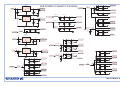
1
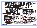
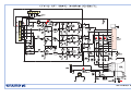
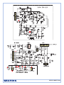
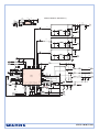
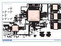
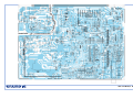
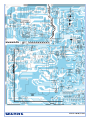
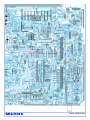
Service Document
STF 72-1010/7 Text
Service
Manual
Sicherheit
Safety
Materialnr./Part No.
720108000001
S
S
Es gelten die Vorschriften und Sicherheitshinweise
gemäß dem Service Manual „Sicherheit“, Materialnummer 720108000001, sowie zusätzlich die eventuell
abweichenden, landesspezifischen Vorschriften!
The regulations and safety instructions shall be valid
as provided by the „Safety“ Service Manual, part
number 720108000001, as well as the respective
national deviations.
Dieses Service Dokument ist nur in Datenform verfügbar
This Service Document is only available as data
Materialnummer / Part Number 720130000400
Änderungen vorbehalten/Subject to alteration
Made by GRUNDIG in Germany • TCC 0107 HH
http://www.grundig.com
GBF2500
STF 72-1010/7 Text
STF 72-1010/7 Text
STF 72-1010/7 Text
ICM01
LD1117V
3
VIN
VOUT
GND
+5V-2
SSB POWER SCHEMATIC DIAGRAM
2
CM10
10u/16V
CM11
CM12
10u/16V
0.1
CM03
GND
VOUT
CM48
22
3V3_S
1
CM38
10u/16V
CM49
390P
CM50
0.1
CM56
22
0.1
CM57
390P
3V3S
LM05 1uH
3V3_S
22
CM96
22
VCC33_IO
CM60
390P
CM61
0.1
VDD33_14
VIN
VOUT
2
CM26
0.1
CM29
390P
CM30
0.1
GND
VCC18_SUB
VDD18_4
GND
VDD18_7
CM44
390P
CM45
0.1
CM46
390P
CM47
0.1
VDD18_11
GND
CM70
100u
3V3A_MCU
CM71
3V3_MCU
100n
LM18 FB VCD18
GND
CN38
VIN
VOUT
1
GND
22
CM74
10u/16V
2
CM78
100u/16V
1V8A_MCU
CM76
100n
LM20 FB VCD33
3V3A_MCU
CN27
390P
CN31
390P
1V8
1V8_MCU
CN50
47uF
CN30
0.1
CN33
390P
CN34
0.1
VCC18_101
GND
VCC18_103
CN28
0.1
CN32
0.1
CN36
390P
CN37
0.1
CN41
390P
CN42
0.1
CN46
390P
CN47
0.1
CN53
390P
CN54
0.1
VDD18_125
CN39
390P
CN40
0.1
CN43
390P
CN44
0.1
VCC18_107
GND
VDD18_112
GND
1V8_MCU
GND
LM19 FB
CN29
390P
1V8A_MCU
ICM04
LD1117V3.3
3
VDD18_17
3.3V
1
GND
3
CM69
10u/16V
3V3M
CM25
390P
ICM03
LD1117V3.3
+5V-1
3V3M
GND
VDD18
CN19
47
GND
GND
LM03 1uH
GND
+5V-1
VCC18_CVBS
VDD33_14
LM12 1uH
CM52
0.1
CM14
0.1
VCC18_DIG
VDD33_24
CM58
0.1
GND
CM51
390P
CM13
390P
GND
VCC18_CLK
VDD33_24
3V3_OUT
GND
CM53
CM05
0.1
VCC18_RGB
VDD18_29
GND
LM06 1uH
CM37
CM04
390P
VDD18_29
3V3_OUT
ICM02
LD1117V
CM02
0.1
GND
1V8_OUT
2
CM01
390P
22
LM04 1uH
VIN
VCC18
1V8_S
1V8_S
GND
3
LM01 1uH
1V8_OUT
1
+5V-2
CN58
CN51
390P
CN52
0.1
CN56
390P
CN57
0.1
VCC33_148
VCC33_157
CM19
GND
VDD18_15
VDD18_100
CM08
390P
CM09
0.1
CM16
390P
CM17
0.1
CM23
390P
CM24
0.1
CM27
390P
CM28
0.1
CM32
390P
CM33
0.1
VDD33_13
GND
VDD33_25
3V3
47uF
VDD33_34
GND
VDD33_47
LM02
3V3_MCU
FB
GND
VDD18_92
VDD18_71
CM98
47uF
GND
CM07
0.1
GND
22
GND
CM06
390P
CM40
390P
VDD33_64
GND
VDD33_82
VDD33_139
CM41
0.1
GND
VDD18_62
STF 72-1010/7 Text
+5V-1
DM05
RM10
10K
YM02
32768Hz
CN77
18p
XP5
2
1
2
1
CN78
18p
CN79
ICM16
1
2
3
4
SSB SCHEMATIC DIAGRAM (1)
4148
OSCI
OSCO
Vbat
Vss
8
7
6
5
VCC
OUT
SCL
SDA
0.1
SCL2
SDA2
GND
8VF
M41T56/M41T81
RE21
330
TJC3-2
GND
CD18
RE17
1K
R_TV
LE02
10uH
8V
CE08
0.1
RE15
470
CE06
100uF/16V
CE15
100uF/16V
GND
220n
QE07
BC857B
RE19
680
LE04
6.8uH
CE14
33p
QE06 GND
BC847B
PR_R
CE12
CE09
RE18
150
12p
104
PR_R
RE16
68
GND
RE26
1K
RE30
330
CD19
RE24
470
G_TV
220n
QE10
BC857B
RE28
680
LE06
6.8uH
CE21
33p
CE16
0.1
GND
QE09
BC847B
Y_G
CE20
CE17
RE27
150
12p
104
Y_G
RE25
68
GND
RE39
330
CD20
B_TV
220n
QE13
BC857B
RE37
680
GND
QE12
BC847B
PB_B
LE08
6.8uH
CE28
CE30
33p
12p
CE25
RE35
150
104
GND
H100
H100
CD14
27P
CD13
10P
RD09
100
CE24
0.1
RE33
470
RE36
1K
PB_B
RE34
68
GND
RD33
V100
32
GND
12
Hsel
Bi1
Ri1
Gi1
FSBCO
Yin
Uin
Vin
DACout
Hd
BL1
VDOa
X
VDOb
RD05
0
NF
Bo
BCL
EWO
CD15
DPC
HFB
RD34
38
RD12
100
41
42
RD13
100
43
RD39
44
CD34
47P
ZDD1
8V2
10K
GND
RD04
100
SCL2
SCL2
1
CD02
102
CD22 CD23
SDA2
2
RD03
100
GND
SDA2
3
4
5
6
8
7
CD03
100n
103
GND
101
GND
GND
GND100
RD35
VDVDVD+
VD+
100
RD36
CD01
102
GND
RD50
330
ABL
IOM
100
CD33
470P
RD14
DD01
1K
4148
GOUT
75
LD13
1uH
BOUT
75
CD41
NC
CD42
NC
ROUT
GOUT
BOUT
CD43
NC
ABL
IOM
GND
LD01
RD16
20K DD02 4148
GND
RD52
330
RD51
330
RD1533K
ZM02
9V1
CD25
104
CD07
100uF
10uH
8V
8V
GND
GND
RD02 RD01
1K5
39K
RD28
EW
RD31 100
EHT
100
LD12
1uH
RD55
RD11
100
40
BLK
QD03
BC847B
GND
10K
39
Go
ROUT
75
RD54
37
Ro
VSC
9
HBLK
13
Iref
RD53
LD11
1uH
QD02
BC847B
36
Vp2
TDA933X
X
HBLK
100n 14
RD06
ICM14
Vp1
EHTin
GND
CD04
BL2
FLASH
GND
100n 15
DECbg
GND1
CD05
16
B2i
DECvd
17
RD07
39K2 1%
CD06
104
G2i
GND
CD21
10P
35
Ri2
GND2
Hout
18
34
PWL
XTALi
SCO
19
SCL
20
SDA
104
XD01
12MHZ
CD09
4.7uF/16V
XTALo
10
CD08
21
LPSU
11
GND
22
27P
Vd
104
CD11
CD40
104
QD01
BC847B
GND
33
30
31
28
29
27
X
25
23
GND
CD10
27P
10K
RD38
3K9
CD12
26
RD08
100
24
V100
HOUT
GND
GND
EW
EHT
HOUT
STF 72-1010/7 Text
SSB SCHEMATIC DIAGRAM (2)
2/CE
4NOT_BE0
6/WE
8/CAS
LED
2ADDR_11
4ADDR_12
6NOT_BE1
8ADDR_13
2 ADDR_6
4 ADDR_7
6 ADDR_8
8 ADDR_9
ADDR_12
ADDR_11
ADDR_10
2
4
6
8
RM58
100
ADDR_19
1
3
5
7
RSM8
8P4R-47
1
3
5
7
1
3
5
7
1
3
5
7
1
3
5
7
2
4
6
8
2
4
6
8
2
4
6
8
2
4
6
8
2
4
6
8
1
3
5
7
RSM12
8P4R-47
/WE
1
3
5
7
1
3
5
7
1
3
5
7
1
3
5
7
1
3
5
7
1
3
5
7
RSM7
8P4R-47
RSM1
8P4R-47
RSM17
8P4R-47
ADDR_8
1
3
5
7
VDD18_62
VDD33_64
VDD18_71
CM97
47uF/16V
GND GND
GND
QM05
BC847B
ADDR_17
ADDR_7
RM79 0
GND
ADDR_18
GND
ADDR_6
ADDR_5
VDD33_47
ADDR_4
ADDR_3
80
79
78
77
76
75
74
73
72
71
70
69
68
67
66
65
64
63
62
61
60
59
58
57
56
55
54
53
52
51
50
49
48
47
46
45
44
43
42
41
4K7
ADDR_13
ADDR_9
1
3
5
7
LED
RM88
LED-1
1
3
5
7
1
3
5
7
RM90
4K7
2ADDR_3
4CKOUT
6ADDR_4
8ADDR_5
2ADDR_10
4ADDR_0
6ADDR_1
8ADDR_2
2 /RAS
4 /CS
6ADDR_15
8ADDR_16
ADDR_17
ADDR_18
ADDR_14
Flash_D15
Flash_D7
ADDR_19
2
4
6
8
RSM10
8P4R-47
1
3
5
7
1
3
5
7
ADDR_14
RSM6
8P4R-47
2
4
6
8
RSM15
8P4R-47
RSM13
8P4R-47
+5V-1
Flash_D14
Flash_D6
Flash_D5
Flash_D13
2
4
6
8
2
4
6
8
Flash_D12
2
4
6
8
2
4
6
8
Flash_D4
ADDR_15
3V3
Flash_D1
Flash_D8
Flash_D0
+5V-1
2
4
6
8
2
4
6
8
1
3
5
7
GND
VDD18_92
8P4R-47
RM87
4K7
VCC18_107
220
YCRCB3
B
49
50
51
52
53
54
55
56
57
58
59
60
61
62
63
64
CN10
220p
RM41
470 %1
VCC18_DIG
GND
VCC33_IO
CN71
CN20
10p
LM17
5.6uH
CN21
120p
CN16 CN17
10uF 390p
100n
GND
RM44
GND
150 1%
100n
CN68
CN67 ICM06
22n
STV2310
10uF
VIDEO
VCC18_RGB
GND_RGB
R_PR
G
B_PB
VCC18_DIG
GND_DIG
GND_IO
VCC33_IO
ADCIN
VIDEOCOMM
VIDEO_OUT
REEP_CVBS
REEM_CVBS
CVBS1_Y
GND_CVBS
CN23 CN24
390p
VIDEO
GND
Y-SVID
GND
GND
GND
VDD18_29
1
3
5
7
VDD33_24
1
3
5
7
VDD18_17
RSM4 8P4R-68
2
1
2
4
3
4
6
5
6
8
7
8
1
3
5
7
2
4
6
8
RM74
NC
47 %1
2
4
6
8
YCRCB1
YCRCB2
YCRCB3
CN61
390P
SW1
RM53
68 %1
SW2
SW2
22P
1
3
5
7
OSD
RM40
RM62
NF
CM75
0.1
0.1
0.1
0.1
0.1
0.1
0.1
Flash_D1
Flash_D2
Flash_D3
Flash_D4
GND
Flash_D5
Flash_D6
Flash_D7
ADDR_18
/WE
/CAS
/RAS
/CS
TILT
ADDR_15
TILT
100
ADDR_16
ADDR_10
ADDR_2
STDBY-1
LED-1
H100
V100
ADDR_3
RM61
IR
IR
8216-RES
8216-RES
SW3
100
YCRCB4
1
2
3
4
YCRCB6
TEST
YCRCB7
CM63
103
RD32
10K
TEST
A0
A1
A2
GND
RD29
10K
CN60
22P
100
RM51
100
8216-RES
RD41
RD40
33K
100
+5V-1
ZDD8
5V6
RM54
3K3
RM55
3K3
GND
ZDD9
5V6
GND
SDA2
SCL2
SDA2
SCL2
+5V-1
CM31
Flash_D3
Flash_D10
0.1
Flash_D2
Flash_D9
GND
Flash_D1
CM18
22u/16V
GND
Flash_D8
Flash_D0
/CAS
/CE
ICM10
HY57V641620HCT-H
54
53
52
51
50
49
48
47
46
45
44
43
42
41
40
39
38
37
36
35
34
33
32
31
30
29
28
VSS
DQ15
VSSQ
DQ14
DQ13
VDDQ
DQ12
DQ11
VSSQ
DQ10
DQ9
VDDQ
DQ8
VSS
NC
UDQM
CLK
CKE
NC
A11
A9
A8
A7
A6
A5
A4
VSS
GND
Flash_D15
Flash_D14
Flash_D13
Flash_D12
Flash_D11
Flash_D10
Flash_D9
Flash_D8
ADDR_19
SDRAM_CLK
ADDR_11
ADDR_9
ADDR_8
ADDR_7
ADDR_6
ADDR_5
ADDR_4
GND
RM63
VCC
WP
SCL
SDA
8
7
6
5
RM80
10K
GND
RM42
3K3
WP
SCL1
SDA1
CM66
CM67
CM68
CM89
CM88
CM90
0.1
0.1
0.1
0.1
0.1
0.1
0.1
DM03
4148
DM04
4148
WP
SCL1
SDA1
GND
SDRAM_D0
SDRAM_D1
SDRAM_D2
SDRAM_D3
GND
RM43
3K3
SDRAM_D4
SDRAM_D5
SDRAM_D7
+5V-1
A0
A1
A2
GND
VCC
WP
SCL
SDA
RM64 1K
/CAS
8
7
6
5
ZDD6
5V6
/RAS
ZDD7
5V6
/CS
ADDR_15
ADDR_16
GND
24C64
ICMA11
ADDR_10
GND
ADDR_0
ADDR_1
ADDR_2
WP
KEY
ADDR_3
RM81
15K
GND
AFT
1
2
3
4
5
6
7
8
9
10
11
12
13
14
15
16
17
18
19
20
21
22
23
24
25
26
27
VDD
DQ0
VDDQ
DQ1
DQ2
VSSQ
DQ3
DQ4
VDDQ
DQ5
DQ6
VSSQ
DQ7
VDD
LDQM
/WE
/CAS
/RAS
/CS
BA0
BA1
A10/AP
A0
A1
A2
A3
VDD
ICM09
HY57V641620HCT-H
VSS
DQ15
VSSQ
DQ14
DQ13
VDDQ
DQ12
DQ11
VSSQ
DQ10
DQ9
VDDQ
DQ8
VSS
NC
UDQM
CLK
CKE
NC
A11
A9
A8
A7
A6
A5
A4
VSS
54
53
52
51
50
49
48
47
46
45
44
43
42
41
40
39
38
37
36
35
34
33
32
31
30
29
28
SDRAM_D15
SDRAM_D14
SDRAM_D13
SDRAM_D12
SDRAM_D11
SDRAM_D10
SDRAM_D9
SDRAM_D8
NOT_BE1
SDRAM_CLK
ADDR_12
ADDR_11
ADDR_9
ADDR_8
ADDR_7
ADDR_6
ADDR_5
ADDR_4
GND
AFT
XP1
SCL2
SDA2
SCL1
SDA1
TEST
100
RM83
21
22
23
24
25
26
27
28
29
30
31
32
33
34
35
36
37
38
39
40
+5V-1
75K
STDBY
IR
GND
LED
8216-RES
XP4
SCL2
SDA2
3V3
Flash_D11
VCD33
RD37 RD30
4K7
4K7
GND
RM50
Flash_D12
Flash_D4
GND
SCART1 SCART1
RM45
4K7
VDD
DQ0
VDDQ
DQ1
DQ2
VSSQ
DQ3
DQ4
VDDQ
DQ5
DQ6
VSSQ
DQ7
VDD
LDQM
/WE
/CAS
/RAS
/CS
BA0
BA1
A10/AP
A0
A1
A2
A3
VDD
CM65
SDRAM_D6
WP
KEY
CN80
1uF/50V
Flash_D5
3V3
CN09
10uF
0.1
GND
GND
XRAY
YCRCB5
Flash_D13
GND
SW3
+5V-1
CN08
6V2
GND
GND
RD76
100
100
1
2
3
4
5
6
7
8
9
10
11
12
13
14
15
16
17
18
19
20
21
22
23
24
25
26
27
100
ICM11
24C64
2
Flash_D14
Flash_D6
GND
2SDRAM_D4
4SDRAM_D5
6SDRAM_D6
8SDRAM_D7
2
4
6
8
CM83
ADDR_1
1
2
3
4
KEY
ROUT
GOUT
TILT
3V3M
BOUT
IOM
TJC3-8
GND
GND
12
RD42
100
VDD18_7
GND
RSM16
1
3
5
7
CM81
Flash_D0
DM02
4148
2SDRAM_D0
4SDRAM_D1
6SDRAM_D2
8SDRAM_D3
2
4
6
8
CM80
ADDR_0
VCC33_148
VCC33_157
Y_G
PR_R
PB_B
OSD
RM38 100
SCART2 SCART2
VDD18_11
CN59
1n
1
3
5
7
GND
MUTE-1
UBASS-1
RM89
RM84
GND
CN62
330P
SW1
VDD33_139
CN55
LM21
2.2u
GND
VDD33_13
TV/AV-1
YCRCB0
RSM5 8P4R-68
VDD33_14
22n
VDD18_4
RSM14
1
3
5
7
VDD18_15
2
4
6
8
CM93
/WE
RM48
100
GND
VDD33_25
GND
PLL_LOCK
GND
RM49
4K7
22P
RM52
C-SVID
XRAY
10K
32
31
30
29
28
27
26
25
24
23
22
21
20
19
18
17
AV1/AV2-1
GND
1
3
5
7
CM92
NOT_BE0
PLL LOCK
CLK_DATA
VSS_OUT
VDD18_OUT
YCRCB0
YCRCB1
YCRCB2
YCRCB3
VDD33_IO
VSS_IO
YCRCB4
YCRCB5
YCRCB6
YCRCB7
VSS
VDD18_CORE
GND
RM39
10KF
CN45
GND
CN63
C-SVID
1
100
RM02
100
Flash_D7
47K
Y_G
PR_R
PR_B
OSD
RM65
GND
Flash_D15
RM57
CM91
DM01
4148
2SDRAM_D12
4SDRAM_D13
6SDRAM_D14
8SDRAM_D15
ZM01
GND
VDD18_125
GND
RM91
VCC18_CVBS
75
Y-SVID
GND
1 2 3 4 5 6 7 8
VCC18_RGB
GND
RSM11
1
3
5
7
+5V-1
2SDRAM_D8
4SDRAM_D9
6SDRAM_D10
8SDRAM_D11
2
4
6
8
1
3
5
7
RM86
H100
V100
GND
48
47
46
45
44
43
42
41
40
39
38
37
36
35
34
33
G
1
3
5
7
GND
VDD33_34
3V3
GND
R
GND
REFM_RGB
REEP_RGB
FB
SHIELD
CLKSEL
CLKXTM
XTALIN_CLKXTP
XTALOUT
GND_CLK
VCC18_CLK
VCC18SUB
GNDSUB
VCC33SUB
FIELD
VSYNC
HSYNC
B
390p
VCC18_CVBS
CVBS2_Y
C
VDD18_CORE
VSS
TST_MODE
VDD18_CORE
VSS
SDA
SCL
VDD18_CORE
VSS
NRESET
VDD33_IO
VSS_IO
I2CADD
G
0.1
RM56
68
1
2
3
4
5
6
7
8
9
10
11
12
13
14
15
16
R
CN04
RM11
390p
0.1
CN03
WP-1
GND
VCC18_SUB
CN02
ICM08
M29W160
ADDR_16
47K
RSM9
+5V-1
RM24
10K
VCC18_CLK
PLL_LOCK
GND
100
YCRCB2
TRST
TV/AV-1
RM72
CN01
YCRCB1
AV1/AV2-1
FB
YCRCB0
MALE 2*10
RM78
10K
FB
TMS
TCK
TDI
TDO
SDA1
GND
+
+
+
+
+
+
+
+
+
+
GND
SDA2
GND
+
+
+
+
+
+
+
+
+
+
1
3
5
7
9
11
13
15
17
19
GND
GND
VDD18_112
40
39
38
37
36
35
34
33
32
31
30
29
28
27
26
25
24
23
22
21
20
19
18
17
16
15
14
13
12
11
10
9
8
7
6
5
4
3
2
1
121
122
123
124
125
126
127
128
129
130
131
132
133
134
135
136
137
138
139
140
141
142
143
144
145
146
147
148
149
150
151
152
153
154
155
156
157
158
159
160
GND
J_DCU
YM01
27MHz
ICM07
stv3500
SCL1
QM12
BC847B
4K7
33
YCRCB4
QM11
BC847B
2
4
6
8
10
12
14
16
18
20
33
RM15
AV 1/AV 2-RD78
1
AV1/AV2
RM20
RM21
10K
4K7
AV1/AV2
TV/AV
CM79
18pF
10K
TV/AV
CM77
18pF
GND
GND
GND
VDD18_100
VCC18_101
GND
VCC18_103
GND
RM14
GND
TV /AV -1 RD77
CM72
103
CM95
10uF/16V
10K
4K7
STDBY
QM04
BC847B
RM13
STDBY-1 RM85
RESET
RM12
STDBY
ADDR_9
ADDR_11
ADDR_12
NOT_BE1
ADDR_13
VSS_IO
VDD33_IO
SDRAM_D8
SDRAM_D9
SDRAM_D10
SDRAM_D11
SDRAM_D12
SDRAM_D13
SDRAM_D14
SDRAM_D15
VDD33_IO
VSS_IO
SDRAM_D0
SDRAM_D1
SDRAM_D2
SDRAM_D3
SDRAM_D4
SDRAM_D5
SDRAM_D6
SDRAM_D7
VDD18_CORE
VSS
VDD33_IO
VSS_IO
PORTA3/PWMCapture3/PWM3
PORTA2/PWMCapture2/INT3/extreg/PWM2
PORTD6/INT0
PORTD3/Timer input3/Timer output2
PORTD2/Timer input2/Timer output3
PORTD1/Timer input1
PORTD0/Timer input0
PORTC4/SDA_2
PORTC5/SCL_2
PORTC6/SDA_3
PORTC7/SCL_3
8P4R-47
1
3
5
7
Flash_D9
GND
48
47
46
45
44
43
42
41
40
39
38
37
36
35
34
33
32
31
30
29
28
27
26
25
A16
/BYTE
GND
Q15/A-1
Q7
Q14
Q6
Q13
Q5
Q12
Q4
VCC
Q11
Q3
Q10
Q2
Q9
Q1
Q8
Q0
/OE
GND
/CE
A0
3V3
8P4R-47
RSM3
4K7
GND
VSS_IO
VDD33_IO
FLASH_D11
FLASH_D3
FLASH_D10
FLASH_D2
FLASH_D9
FLASH_D1
FLASH_D8
FLASH_D0
VSS
VDD18_CORE
TMS
TCK
TDO
TDI
TRST
NRESET
VSS
VDD18_CORE
VCC18_IO
GND_IO
VCC18_PLL3
GND_PLL3
XTALIN
XTALOUT
VCC18_PLL1
GND_PLL1
CLKXTM
CLKXTP
VSS_PLL
VDD18_PLL
SHIELD_PLL
VSYNC
HSYNC
CLK_DATA
YCRCB0
YCRCB1
YCRCB2
YCRCB3
A15
A14
A13
A12
A11
A10
A9
A8
NC
NC
/WE
/RESET
NC
NC
RY/(/BY)
A18
A17
A7
A6
A5
A4
A3
A2
A1
ADDR_0
8P4R-47
81
82
83
84
85
86
87
88
89
90
91
92
93
94
95
96
97
98
99
100
101
102
103
104
105
106
107
108
109
110
111
112
113
114
115
116
117
118
119
120
GND
VDD33_82
8P4R-47
UBASS
SCL2
4K7
UBASS
10u/16V
YCRCB7
UBASS-1 RM32
QM03
BC847B
Flash_D2
QM02
BC847B
CM36
2
4
6
8
2
4
6
8
YCRCB6
MUTE
1
3
5
7
YCRCB5
MUTE-1 RM31
Flash_D10
RM33
4K7
MUTE
1
3
5
7
8P4R-47
Flash_D3
FLASH_D4
FLASH_D12
FLASH_D5
FLASH_D13
FLASH_D6
FLASH_D14
FLASH_D7
FLASH_D15
VSS
VDD18_CORE
ADDR_14
ADDR_19
ADDR_18
ADDR_17
NOT_CS_FLASH
VSS_IO
VDD33_IO
VSS
VDD18_CORE
NOT_BE0
RD_NOTWR
NOT_CAS
NOT_RAS
NOT_CS_SDRAM
ADDR_15
ADDR_16
ADDR_10
ADDR_0
ADDR_1
ADDR_2
ADDR_3
CKIN_SDRAM
VSS_IO
VDD33_IO
CKOUT_SDRAM
ADDR_4
ADDR_5
ADDR_6
ADDR_7
ADDR_8
Flash_D11
YCRCB4
YCRCB5
YCRCB6
YCRCB7
VDD18_CORE
VSS
PORTC3/SCL_1
PORTC2/SDA_1
PORTC1/SCL_0
PORTC0/SDA_0
PORTA0/PWMCapture0/PWM0
PORTD4/IR_In
PORTA1/PWMCapture/INT2/PWM1
PORTD7/INT1/16xUART clock
PORTA4/TXD
PORTA5/RXD
PORTA6/CTS
PORTA7/RTS
VDD33_IO
VSS_IO
PORTB5/AD_5/Timer output1
PORTB4/AD_4/Timer output0
PORTB3/AD_3
PORTB2/AD_2
PORTB1/AD_1
PORTB0/AD_0
PORTD5/GFX_ACTIVE
VCC33_ADC
GND_ADC
SHIELD_ADCDAC
REXT
GND_REXT
PB_B
PR_R
Y_G
GND_DAC
VCC33_DAC
V100
H100
CLK_DFL
RSM2
+5V-1
RM35
4K7
ADDR_2
ADDR_1
GND
+5V-1
1
2
3
4
5
6
7
8
9
10
11
12
13
14
15
16
17
18
19
20
21
22
23
24
XP2
8216-RES
20
19
18
17
16
15
14
13
12
11
10
9
8
7
6
5
4
3
2
1
12V
MUTE
UBASS
+5V-1
STDBY
XRAY
HBLK
EW
HOUT
VD+
VDABL
EHT
21
22
23
24
25
26
27
28
29
30
31
32
33
34
35
36
37
38
39
40
8V
+5V-2
CM62
103
AV1/AV2
TV/AV
AFT
SW3
SW2
SW1
VIDEO
GND
C-SVID
DCON40
GND
20
19
18
17
16
15
14
13
12
11
10
9
8
7
6
5
4
3
2
1
SCART1
SCART2
12V
8V
+5V-2
FB
R
B
G
Y-SVID
DCON40
GND
GND
GND
GND
STF 72-1010/7 Text
STF 72-1010/7 Text
STF 72-1010/7 Text
STF 72-1010/7 Text
SPECIFICATION
SYSTEM.......................... PAL,SECAM, B/G, D/K NIACAM STEREO POWER INPUT..............................................AC 170-260V(50/60Hz)
POWER CONSUMPTION......................................................... 120W
AERIAL IMPEDANCE.................................. 75 OHM UNVALANCED
TUNER...................................... VOLTAGE SYNTHESIZER TUNING
RECEIVING CHANNELS............................................ VHF-L E2-S10
....................................................................................VHF-H E5-S41
..................................................................................... UHF E21-E69
PROGRAMME............................. MAX.255 PROGRAM MEMORIES
PICTURE TUBE.............................................................................29”
SOUND OUTPUT.........................................................................≥5W
AV JACKS................................... 2 FULL SCART, SIDE RCA INPUT
Chassis Adjustment:
General description of method to enter into SERVICE MENU and ADJUST MENU:
- Turn on the Main Power Switch, then press “FACTORY” key about 3 seconds on the handset (service remote unit, please refer to the attached drawing). The “HPS ----------- Geometry Adjust” will be displayed on the screen: When receiving signal is 50Hz, the “100i” will be displayed under the
“Geometry Adjust”, otherwise, when receiving the 60Hz signal, the “60P” will be displayed instead of “100i”.
- Use volume “+” and “-” keys to adjust the parameter.
- Pressing channel “P+” and “P-” key select other items;
- On Geometry Adjust mode, refer to the follow table 1 to find adjustment items.
- Press “FACTORY” KEY again, The “RCUT -----------White Balance” will be displayed on the screen:
- On White Balance mode, refer to the follow table1 to find adjustment items.
- Repeat the above step and
- press “FACTORY” KEY to exit the adjustment menu.
B+ adjustment:
- Receive standard colour bar signal.
- Press key "PP." to select “NORMAL” mode.
- Connect digital voltmeter between of C922 and GND.
- +B voltage:
CRT BRAND
CRT TYPE
B+ (C922)
THOMSON
A68ELM021x121
133.0V
Connect the DC digital voltmeter to the C922 on main PCB. Receving the Color bar signal, and press the P.P button to select “Normal” status. Adjust
the VR901, to make the reading of the DC digital voltmeter as above table.
IC901 power check:
- Connect probe of oscillograph to C911+ and GND;
- The read-out voltage on oscillograph must be directly voltage, the value should be 10.5~15VDC.
STAND-BY power supply check
- Connect the digital voltmeter between C924 and GND;
- Press power key on remote unit to make sure the TV is on standby mode;
- The read-out on the digital voltmeter must be 8.0~10VDC
Adjustment for RF AGC:
- Receive RF signal (62±3dBµV).
- Press factory key to enter Geometry Adjust MENU.
- Press “1” keys on the remote handset and on-screen display will be shown as following:
AGC Geometry Adjust
XX 100i - Press volume "+" or "-" on the remote handset to change the value of RF AGC until snow noise on the screen just disappears.
- Press “FACTORY ” key to exit.
STF 72-1010/7 Text
Set Adjustment
The Geometry adjustment:
Input the 50Hz signal, and entering the Factory Menu by pressing the Factory button on the remote. Then the key’s function on the remote handset is
like as following table 1, You can adjust the parameters of the 50Hz(100i) Geometry. Then change the input signal to 60Hz, and repeat adjusting the
parameters of the 60Hz Geometry. Repeat pressing the Factory button to exit the Factory Menu.
Table 1
Key
Geometry Adjustment Menu
White Balance
Menu state
Mute
Mute
AV
TV/AV
TBright
Auto Scan
Auto search programmer
Standby
Standby
Standby
TV/AV
Standby
1
AGC
RF AGC Adj.
RCUT-
2
OSDP
OSD Position
RCUT+
3
HPS
Hor. Position
RDRV-
4
VP50
Vertical Center
RDRV+
5
HIT
Vertical Amplitude
GCUT-
6
VSC
Vertical S-correction
GCUT+
7
VLIN
Vertical linearity
GDRV-
8
BOW
9
WID
Horizontal Amplitude
Sub-brightness-
GDRV+
0
DPC
Pincushion correction
Sub-brightness+
_/__
PARA
Parallelogram correction
BDBD+
I/II
KEY
Keystone correction
Swap
UCNR
Up corner correction
Sleep
LCNR
Low corner correction
Display
EHT
EHT
Game
TXTHPS
Teletext Hor. Position
Menu
TXTVPS
Teletext Vert. Position
P.P
Picture Preference
S.P.
Sound Preference
OK
Save Factory default
Picture Preference
Save Factory default
V+
Adjust Increase
Adjust Increase
V-
Adjust Decrease
Adjust Decrease
P+
Select previous item
Select previous item
P-
Select next item
Select next item
TXT
Freeze
Mode
Bri/Contrast
Zoom
Color system direct key
Index
Sound system direct key
Hold
Reveal
Retrieve Geometry Default Value
Retrieve WB Default Value
Mix
Factory
Burn
Design
BusOff
STF 72-1010/7 Text
Focus Adjust
- Press key "P.P." on the remote handset to set the TV on NORMAL mode.
- Adjust knob "FOCUS" on FBT to make the picture on the screen to be the most distinct.
G2 alignment:
Press the Design button on the remote handset and hold about 4seconds to enter the Designer Menu, use the P+ or P- key to select the item of G2Alignment. Then press the V+(right cursor), then the screen be display INCREASE or DECREASE or OK. If INCREASE or DECREASE be displayed ,
please adjust the SCREEN button on the FBT until the screen displayed is OK. Repeat press the Design button to exit the Designer Menu.
White-Balance adjustment:
- Press the Factory button on the remote handset two times to enter White Balance adjust mode, this moment, the key’s function on the remote is like
as Table 1.
- Adjust Red Gain (RDRV), Green Gain (GDRV), Blue Gain (BDRV), DC Red (RCUT), DC Green (GCUT), DC Blue (BCUT) until the white-balance
meet the requirement.
- Press Factory button to exit White Balance adjust mode.
Horizontal/Vertical center adjust:
- Receive MONOSCOPE PATTERN.
- Enter Geometry Adjust mode;
- Use remote to get Hor- Position (HPS) item, use VOL+/- buttons to set Hor-center of the picture to meet the standard requirement.
- Use remote to get Ver.- center item, use Vol+/- keys to set ver-center of the picture to meet the standard requirement.
Vertical amplitude adjust:
The set have to adjust 50Hz and 60Hz single Ver-amplitude.
- Enter Geometry Adjust model;
- Input 50Hz signal, adjust HIT until amplitude meet the standard.
- Input 60Hz signal , adjust HIT until amplitude meet the standard.
Sub-brightness adjust:
- Receive GREY SCALE/COLOR BAR pattern.
- Press the P.P. key to select the state of “normal”.
- Enter Service White Balance mode.
- Get Sub- Bright Min tem. Press VOL+/- buttons to make the second darkness bar of GREY SCALE part loom. Press
- Exit this mode by press FACTORY key.
E-W correction and Hor.-wide adjustment:
- Press P.P. key on remote unit to set TV on normal state.
- Enter Geometry Adjust mode;
- Input a 50Hz crosshatch pattern signal to the TV set ;
- press 9 key on remote to get WID item, press VOL+/VOL- to make the crosshatch pattern just be full of the CRT screen;
- Press “0” key on remote unit to get DPC item, then press VOL+/VOL- key on remote carefully to make the vertical lines of the pattern become straight
as possible.
- Press “-/-“ key to get PARA item, then press VOL+/VOL- key to make the picture like as square;
- press “AV” key to get KEY item, press VOL+/VOL- key carefully to make the picture on the screen is same width from top to bottom.
- Press “SWAP” key to get UCNR item, then press VOL+/VOL- key carefully to make the vertical lines on the top corner of CRT screen become
straight.
- Press “SLEEP” key to get LCNR item, then press VOL+/VOL- key carefully to make the vertical line on bottom corner of CRT screen become
straight.
- Input a 60Hz crosshatch pattern signal to the TV set;
- Repeat the above step ~ ;
- Exit Geometry Adjust mode by press factory key on remote unit.
EHT adjustment
- Press ”P.P.” key on remote unit and set TV on normal state.
- Enter Geometry Adjust mode;
- Input a 50Hz crosshatch pattern signal to the TV set
- Adjust EHT till the level width same as diamond signal width.
- Input 60HZ diamond signal;
- Input 50HZ white diamond signal,and adjust EHT till the level width same as diamond signal width;
- Exit geometry adjust mode.
Teletext TV amplitude、horizontal and vertical adjust
- Receive PAL B/G signal;
- Press TV/TXT on remote control enter into teletext mode;
- Press T.BRI on remote control till teletext TV obtain brightness.;
- Press“FACTORY”button into teletext mode,press P+ or P- to choose teletext mode ,HIT, TXTVPS or TXTHPS.
- Select“HIT”item,press VOL+/VOL- button to make vertical amplitude of teletext TV picture reach standard
- Select “TXTVPS”item,pressVOL+/VOL- button to make vertical location of teletext TV picture reach standard .
- Select“TXTHPS”item, press VOL+/VOL- button to make horizontal location of teletext TV picture reach standard .
- Press“FACTORY”button to retreat from teletext geometry adjusting mode.
STF 72-1010/7 Text
Burn button’s introduction:
“aging state” is an independent estate ,the purpose is to make CRT become aging in valid and insure the correct adjustment for white balance.
The method of entering “aging state” - first press “BURN”button into geometry adjustment menu.
The method of exiting “aging state”:
- press “burn button” for 2s to exit.
- set aging time and it will exit the state after set time.(pretermit is 30 minutes,max is 2 hours and can be adjusted under DESIGN MENU)。
Sound is set to quiet state, brightness、contrast and color set to mediate value when TV enter into aging state.Bule screen 、black background function
is switched off,and red letter ”M” displays on the top left corner of screen.
In the “aging state’’ ,any other buttons on remote control is unvalid except “BURN”button.(avoid carelessly pressing standby button enter standby
mode or pressing burn button into aging state). Even if power on again after power off ,but TV is still under aging state ,and it can exit this state till
after set time of aging time.
Bus off state’s introduction:
Press“FACTORY”key ,first enter white balance menu ,then press“BUS-OFF”enter BUS-OFF”state.In this state, CPU will emit I2C bus.This time,I2C
bus will be under outer computer control in order to obtain automatic adjustment of white balance function and automatic adjustment of geometry
parameter function.
DESIGN MENU’s introduction:
Press “Design” button for 3s enter“Design”menu,this menu have the following structure system,and the menu will display in order by pressing “DESIGN”
button. Some functions have several chioses,different function choices adapt to different customers and distribution areas.
Description of the Function option :
RF SECAM L/L' enable/disable:
Option in Designer menu.
Game on/off & select:
Option in Designer menu.
World wide clock on/off:
Option in Designer menu.
Calculator on/off:
Option in Designer menu.
Calendar on/off:
Option in Designer menu.
OSD Language display selection:
Option in Designer menu.
Blue stretch near white on/off:
Option in Designer menu.
4:3/16:9 for CRT:
Option in Designer menu.
AV2: (VIDEO+RGB)/S-VIDEO:
Option in User menu.
LIST mode of TEXT:
Option in Designer menu.
CTI on/off:
Option in Designer menu.
Chroma Coring on/off:
Option in Designer menu.
Comb filter on/off:
Option in Designer menu
Contrast Enhancer off/Black stretch/White stretch/Grey Stretch/Grey StB&W/Auto:
Option in Designer menu.
Green Boost on/off:Option in Designer menu.
Smart Volume on/off:
Option in Designer menu.
Blue stretch on/off:
Option in Designer menu.
Teletext language region option 0—6:
Option in Designer menu.
STV8216Detect Auto/off
Option in DESIGN MENU.
Auto: After select FM Mono by pressing I/II button ,then TV signal is from faint to distinctive ,8126 will identify whether have Nicam,and it will
switch into Nicam Stereo automatically if have.
Off: After select FM Mono by pressing I/II button ,then TV signal is from faint to distinctive ,8126 will identify whether have Nicam broardcast,
and it will be under FM Mono state all the time.
Tumer type option KSH148EA
Option in DESIGN MENU
SP-Y5ED
XG-6F6126CWA
XG-6FT126J
Mono In On/off
Option in DESIGN MENU
On: When under FM / AM Mono,use TDA9886 volume output。
Off: When under FM / AM Mono,use STV8216 inner decode output。
Auto cutoff Loop
Option in Designer menu.
STF 72-1010/7 Text